Embed Size (px)
Citation preview

REPORT◥
DEVICE TECHNOLOGY
Scaling carbon nanotubecomplementary transistorsto 5-nm gate lengthsChenguang Qiu, Zhiyong Zhang,* Mengmeng Xiao, Yingjun Yang,Donglai Zhong, Lian-Mao Peng*
High-performance top-gated carbon nanotube field-effect transistors (CNT FETs) witha gate length of 5 nanometers can be fabricated that perform better than siliconcomplementary metal-oxide semiconductor (CMOS) FETs at the same scale. A scalingtrend study revealed that the scaled CNT-based devices, which use graphene contacts,can operate much faster and at much lower supply voltage (0.4 versus 0.7 volts) and withmuch smaller subthreshold slope (typically 73 millivolts per decade). The 5-nanometerCNT FETs approached the quantum limit of FETs by using only one electron per switchingoperation. In addition, the contact length of the CNT CMOS devices was also scaleddown to 25 nanometers, and a CMOS inverter with a total pitch size of 240 nanometerswas also demonstrated.
Silicon complementary metal-oxide semi-conductor (CMOS) technology will soonreach its performance limits at the sub–10 nm technology node (1–7). Semiconductingsingle-wall carbon nanotube (s-SWCNT)–
based field-effect transistors (FETs) have beenconsidered for sub–10 nm technology nodes be-cause of their nanoscale dimensions, high carriermobility, and excellent stability (4, 8, 9), whichin principle could provide much better scalingproperties and improved on-state performancethan CMOS FETs based on Si and other semi-conductors (e.g., Ge or InGaAs with the samegate length) (10–14). Carbon nanotube (CNT)–based CMOS FETs have been fabricated andshown to possess certain advantages over Si CMOSFETs with channel lengths greater than 50 nm(15, 16) and have been scaled down to 20 nmusing a gate-all-around structure, albeit with lim-ited performance (17). Moreover, excellent scalingbehavior has been demonstrated down to 9 nmfor p-type FETs with a simple local back-gatestructure (18, 19). However, sub–10 nm CNTCMOS FETs have not been reported, and no un-ambiguous performance advantage has beenshown over state-of-the-art Si CMOS FETs forsub–10 nm technology nodes. Although the ulti-mate performance of CNT-based CMOS FETs hasbeen assessed (8), these studies are based mainlyon theoretical simulations or extrapolations fromexperimental results obtained for larger devices.
We report the fabrication of high-performanceCNT CMOS FETs with a gate length scaled downto <10 nm using a doping-free process and a topgate structure, and we explore the scaling be-havior and potential of CNT FETs. The scaledCNT CMOS FETs exhibited higher intrinsic per-formance and lower power consumption thanSi CMOS FETs with a similar gate length but ata lower supply voltage (Vdd). At the 5-nm gatelength, although CNT FETs with an excellent on-state performance can be fabricated with conven-tional metal contacts, the off-state propertiesof these devices are generally compromised.Graphene-contacted CNTFETs are thus proposedand demonstrated to feature a slightly reducedon-state current but a substantially improved off-state performance. We then explore the contactlength scaling behavior for CNT CMOS FETs andpresent a CMOS inverter with a total pitch sizeof 240 nm, which is smaller than that of Si at the22-nm technology node. Our results show thatCNT CMOS technology can yield FETs with a per-formance that approaches that of an ultimatebinary switch with limits imposed by thermody-namics and quantum mechanics.To explore the scaling limit of CNT FETs, we
used individual s-SWCNTs to construct FETs. Al-though this type of material is not suitable forbuilding large-scale integrated circuits (ICs), it iswell defined and most appropriate for exploringthe scaling limit of CNT FETs because deviceswith different channel lengths but identical ma-terial parameters can be fabricated on the sames-SWCNT. A similar approach has been used forinvestigating gate length and contact scaling (17–19).We used a well-developed doping-free processto fabricate complementary FETs on preselecteds-SWCNTs with a top gate structure (11, 15). The
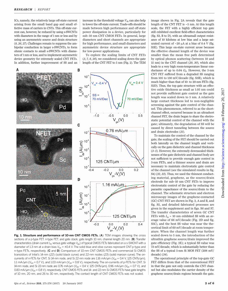
structure and fabrication process flow of theCNT CMOS FETs are shown in fig. S1, togetherwith three cross-sectional transmission electronmicroscopy (TEM) images (Fig. 1A) showing ap-type FET, an n-type FET, and the gate stackstructure of these devices. The transfer (Fig. 1B)and output (fig. S2C) characteristics are shownfor a pair of 10-nm CMOS FETs fabricated on thesame s-SWCNT. A subthreshold slope (SS) of70 mV/decade was obtained for both n-type andp-type FETs [the requirement on SS is smallerthan 80mV/decade for commercial Si CMOS de-vices] and was much lower than that of previ-ously reported short-channel p-type CNT FETs[larger than 90mV/decade for 9-nm p-FET] (19),indicating excellent gate control from the top gateon the 10-nmCNT channel beneath the gate. Thiselectrostatic potential control on the conductingchannel in our devices was enabled by the ultra-thin body of the CNT and the highly efficient gatewith ultrathin HfO2 of 3.5 nm (Fig. 1A) (20). Then-type and p-type FETs in Fig. 1 exhibit nearlysymmetric performance because of the symmetryin both mobility and injection efficiency betweenelectrons and holes in the CNTs (15). Large trans-conductances were also achieved in both n-typeand p-type FETs, andwe observed up to 55 mS perCNT for the n-type FET (fig. S2A), compared with45 mS per CNT for previously reported n-type CNTFETs [(21), gate-all-around structure] and compa-rable to that of the highest-performing p-typeFETs (55 mS per CNT) (19). At a relatively low biasof 0.4V, the on-state current Ids is as high as 17.5 mAfor the p-type FET and 20 mA for the n-type FET(Fig. 1B and fig. S2C), demonstrating the potentialfor low-power applications with very low supplyvoltage (e.g., 0.4 V). The on-state performanceoriginates primarily from the perfect ohmic con-tacts and is manifested in the high output con-ductance of more than 0.5 G0 at low bias (whereG0 is the quantum limit for conductance of a s-SWCNT) for bothn-type andp-typeFETs (fig. S2A).To evaluate the relative performance of CNT
CMOS FETs against that of their Si counterparts,we compared typical transfer characteristics ofCNTCMOSFETs to those of Intel’s 14- and 22-nmSi CMOS FETs, which are the highest-performingFETs reported to date (22, 23). The direct com-parison betweenCNTandSi CMOSFETs is shownin Fig. 1, C and D, in which the current density ofCNTFETs isnormalizedbyassuming 125CNTs/mm(24, 25). The 10-nm CNT CMOS FETs exhibitedhigher on-state current even at a much smallersupply voltage than that of the Si CMOS FETs(0.4 V versus 0.7 and 0.8 V), as well as smalleraverage SS than Si CMOS FETs. Quantitatively,10-nm CNT CMOS FETs powered at 0.4 V canprovide comparable on-state current with thatof state-of-the-art Si CMOS FETs at the 14-nmtechnology node powered at 0.7 V; lowering thesupply voltagewhilemaintaining or even improv-ing performance is the primary goal for scalingdown transistors (3, 4).Although both high on-state performance and
low SS have been demonstrated in 10-nm CNTCMOSFETs, there remains a potential obstacle forthe application of these CNT FETs in low-power
RESEARCH
Qiu et al., Science 355, 271-276 (2017) 20 January 2017 1 of 6
Key Laboratory for the Physics and Chemistry ofNanodevices and Department of Electronics, PekingUniversity, Beijing 100871, China.*Corresponding author. Email: [email protected] (Z.Z.);[email protected] (L.-M.P.)
on
Febr
uary
20,
201
7ht
tp://
scie
nce.
scie
ncem
ag.o
rg/
Dow
nloa
ded
from
ICs, namely, the relatively large off-state currentarising from the small band gap and small ef-fective mass of carriers in CNTs. This off-state cur-rent can, however, be reduced by using s-SWCNTswith diameters in the range of 1 nm or less and byusing an asymmetric source and drain structure(8, 26, 27). Challenges remain to suppress the am-bipolar conduction in larger s-SWCNTs, to formohmic contacts to small s-SWCNTs with diame-ters of 1 nm or less, and to implement asymmetricdevice geometry for extremely scaled CNT FETs.In addition, further improvement of SS and an
increase in the threshold voltageVth can also helpto lower the off-state current. Trade-offs should bemade between high performance and off-statepower dissipation in a device, particularly forsub–10 nm CNT CMOS FETs. In general, largediameters and short channels are appropriatefor high performance, and small diameters andasymmetric device structure are appropriatefor low-power applications.To explore the scaling limits of CNT FETs
(3, 7, 8, 28), we considered scaling down the gatelength of the CNT FET to 5 nm (Fig. 2). The TEM
image shown in Fig. 2A reveals that the gatelength of the CNT FET is ~5 nm. At this lengthscale, the FET with a highly efficient top gatestill exhibited excellent field-effect characteristics(fig. S3, B to D), with an ultrasmall output resist-ance of 10 kilohms at low bias and a large sat-urated current of ~20 mA at a bias of 0.4 V (fig.S3E). This large on-state current arose becausethe effective channel length of the device wassmaller than the mean free path determinedby optical phonon scattering (between 10 and15 nm) in the CNT channel (29, 30), which alsoleads to a very high room-temperature linear con-ductance of up to 0.64 G0. However, the 5-nmCNT FET suffered from a degraded SS rangingfrom 105 to 130 mV/decade (fig. S3B), which ismuch higher than that of 10- to 20-nm FETs (fig.S2D). Thus, the top gate structure with an effec-tive oxide thickness as small as 1.05 nm couldnot provide sufficient gate control as the gatelength was scaled down to 5 nm. A relativelylarge contact thickness led to non-negligiblescreening against the gate control of the chan-nel. This phenomenon, referred to as the short-channel effect, occurred because in an ultrashortchannel FET, the drain began to share the electro-static potential control of the channel with thegate; ultimately, the degradation of SS will becaused by direct tunneling between the sourceand drain electrodes (31).To maintain the control of the channel by the
gate, the scaling of the FET should be carried outboth laterally on the channel length and verti-cally on the gate dielectric and channel thickness(3–5). However, the extremely downscaled thick-nesses of the gate dielectric and channel body arenot sufficient to provide enough gate control in5-nm FETs, and a thinner source and drain arenecessary to maintain electrostatic gate controlof the channel (see the simulated results in fig.S4) (32, 33). Thus, we used the thinnest conduct-ing material, graphene, as the source/drainelectrode for sub–10 nm CNT FETs to improveelectrostatic control of the gate by reducing theparasitic capacitance of the source/drain to thechannel. The schematic structure and electronmicroscopy images of the graphene-contacted(GC) CNT FET are shown in Fig. 2, A and B, andfig. S5, and detailed fabricated processes aregiven in the supplement and in figs. S6 and S7.The transfer characteristics of seven GC CNTFETs with Lg = 10 nm exhibited SS with an av-erage value of 66 mV/decade (Fig. 2D and fig.S5C), and the best SS value was near the the-oretical limit of 60mV/decade at room temper-ature. When the channel length was furtherscaled down to 5 nm, the introduction of theultrathin graphene source/drain improved thegate efficiency (Fig. 2E); a typical SS value was73 mV/decade, which is substantially better thanthe SS of a typical 5-nm Si MOS FET (208 mV/decade) (34).The operational principle of the top-gate GC
FET differs from that of the conventional FETin that the gate not only controls the CNT chan-nel but also modulates the carrier density of thegraphene source/drain regions beneath the gate.
Qiu et al., Science 355, 271-276 (2017) 20 January 2017 2 of 6
Fig. 1. Structure and performance of 10-nm CNT CMOS FETs. (A) TEM images showing the crosssections of a p-type FET, n-type FET, and gate stack; gate length 10 nm, channel length 20 nm. (B) Transfercharacteristics (drain current Ids versus gate voltage Vgs) of typical CMOS FETs fabricated on a s-SWCNTwith adiameter of 1.3 nm at a drain bias Vds = ±0.4 V.The solid blue and olive curves represent CNTp-type andn-type FETs, respectively. (C and D) Comparison of 10-nm CNT CMOS FETs and commercial Si CMOStransistors of Intel’s 14-nm (22) (solid black curve) and 22-nm nodes (23) (solid maroon curve). The on-currents of n-FETs for CNT, Si 14-nm node, and Si 22-nm node are 1.16 mA/mm (Vdd = 0.4 V, 125 CNTs/mm),1.1 mA/mm (Vdd = 0.7 V), and 1.03 mA/mm (Vdd = 0.8 V), respectively.The on-currents of p-FETs for CNT, Si14-nm node, and Si 22-nm node are 0.76 mA/mm (Vdd = 0.4 V, 125 CNTs/mm), 0.96 mA/mm (Vdd = 0.7 V), and0.83mA/mm (Vdd = 0.8 V), respectively. CNTCMOS FETs and 14- and 22-nm Si CMOS FETs have gate lengthsof 10 nm, 20 nm, and 26 to 30 nm, respectively. The contact length of CNT CMOS FETs was not scaled.
RESEARCH | REPORT
on
Febr
uary
20,
201
7ht
tp://
scie
nce.
scie
ncem
ag.o
rg/
Dow
nloa
ded
from

A numerical simulation for the short-channelCNT FETs with a Pd local back-gate geometryshowed that the back gate strongly modulatedthe contact properties, allowing for the realizationof superior subthreshold swings for short-channeldevices (35). In addition, the weak electrostaticscreening of graphene helps to enhance the gatecontrollability on the CNT channel between thegraphene contacts, thus reducing the short-channeleffect (fig. S4). When the device is switched toits on-state, the GC FET becomes a ballistic FETwith a 5-nm channel (Fig. 2C, top). On the otherhand, when in its off-state, part of the CNT out-side the 5-nm channel but below the gate is alsodepleted by the gate; the gate-induced barrier thusbecomes broader than the channel length, lead-ing to suppression of direct tunneling betweenthe source and drain or improved off-state per-formance (Fig. 2C, bottom).An ideal high-performance FET should exhibit
a large on-state current Ion, small off-state cur-rent Ioff, and small SS for fixed gate length Lg andsupply voltage Vdd. We compared the perform-ance of our CNT CMOS FETs with that of thehighest-performing small CNT FETs (Fig. 3A). Ionis defined as the current at |Vgs –Vth| = 0.4 V for asupply voltage of |Vdd| = 0.4 V (17). Figure 3Ashows that our CNT CMOS FETs can typicallyprovide Ion values in the range of 5 to 15 mA,which is much larger than most of the publishedCNTFETswith a similar or smallerLg (17–19, 36).The scaling of SS with Lg of our CNT CMOS FETs(Fig. 3B) also compares favorably with the best
reported FETs, including CNT FETs and state-of-the-art silicon CMOS FETs (17–19, 22, 23, 36–38).In particular, some of our CNT CMOS FETs ex-hibited very small SS even when being scaleddown to 5 nm, which we attributed to the im-proved gate control on the channel and sup-pressed direct tunneling between the source anddrain. The scaling trend of SS of our CNT CMOSFETs is obviously better [SS about 73 mV/decadeversus beyond 100 mV/decade for 5-nm gatelength] than that of planar SiMOS FETs and Fin-FETs (37).To benchmark CMOS FETs based on CNTs
and Si, we used the Intel methodology and keydevice metrics, including intrinsic gate delay (ameasure of intrinsic speed) and energy-delay pro-ducts (EDPs, a measure of switching energy) (37).Both p-type and n-type CNT FETs exhibited smallerintrinsic gate delays than that of the correspond-ing Si FETs with a 10-nm gate length by a factorof ~5 to 10; however, a very small Vdd of 0.4 Vwas used for the CNT FETs, whereas a muchlarger Vdd of 0.7 V was used for the Si devices(Fig. 3C and fig. S8A). In particular, the intrinsicgate delays of the CNT devices were 90 and 57 fsfor the 10-nm p-type and n-type FETs, respec-tively, and this delay was further reduced to43 fs for the 5-nm p-type CNT FETs. In com-parison, the ultimate intrinsic gate delay forSi FETs is projected to be 100 fs by the 2013International Technology Roadmap for Semi-conductors (ITRS) in 2026 for the Si FET withLg = 5.9 nm (39). The realized gate delay of 43 fs
in the 5-nm CNT FET is already near that of thetheoretical speed limit of a binary switch deter-mined by the Heisenberg uncertainty principle(4, 6, 40, 41). Figure 3D and fig. S8B show thescaling trends of the CNT and Si CMOS FETsin terms of the EDP, which is usually used tobenchmark the available parameter space whenconsidering trade-offs between speed and dynamicpower in designing a transistor. The EDP in CNTCMOS FETs is lower than that in Si CMOS FETsby approximately an order of magnitude for thesame Lg. The 10-nm CNT CMOS FETs exhibitEDPs as low as 1.88 × 10⁻³⁰ Js/mm, which issubstantially lower than the predicted limit ofa Si n-type FET at the end of ITRS (39). Theperformance advantages of CNT CMOS FETs overSi CMOS FETs mainly originate from the smallerintrinsic gate capacitance, thin body, and highercarrier mobility of the CNT channel. Additionally,the lower Vdd increases the advantageous EDPfor CNT CMOS by a factor of ~10 relative to thatof Si CMOS devices with the same gate length.As an irreversible binary switch, the scaling
of the FET will eventually reach an absoluteperformance limit given by the Shannon–vonNeumann–Landauer (SNL) expression and theuncertainty principle (4, 6). Indeed, the gate length,intrinsic gate delay, and EDP of our 10-nm and5-nm CNT FETs are already near the correspond-ing theoretical limits of a binary switch (6). Inparticular, the gate delay of the 5-nm CNT FETis scaled down to 43 fs, which should be comparedwith the theoretical limit of 40 fs. Table 1 also
Qiu et al., Science 355, 271-276 (2017) 20 January 2017 3 of 6
Fig. 2. Structure and performance of 5-nmCNT FETs. (A) Top: TEM image of a normal Pd-contacted CNT FETwith gate length of 5 nm. Bottom: SEM imageof a graphene-contacted CNT FETwith channel length of 5 nm, before the deposition of the top gate electrode. (B) Schematic diagram showing the structure ofa GC CNT FET. (C) Schematic band diagrams of the graphene-contacted CNT FET in its on-state (top) and off-state (bottom). EFS and EFD are the Fermi levelsof source and drain graphene electrodes, respectively. (D) Transfer characteristics of three typical GC CNT FETs with Lg = 10 nm and a typical SS of 60 mV/decade at Vds = −0.1 V. (E) Transfer characteristics of three typical GC CNT FETs with Lg = 5 nm and a typical SS of 73 mV/decade at Vds = −0.1 V.
RESEARCH | REPORT
on
Febr
uary
20,
201
7ht
tp://
scie
nce.
scie
ncem
ag.o
rg/
Dow
nloa
ded
from
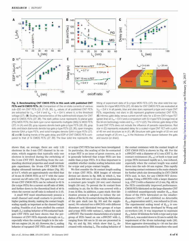
shows that, on average, there are only 1.35electrons in the 5-nm CNT channel in its on-state, which suggests that typically only oneelectron is involved during the switching ofthe 5-nm CNT FET. Benefiting from the out-standing electrical properties and small intrinsicgate capacitance, the 10-nm CNT CMOS FETsdisplay ultrasmall intrinsic gate delays (Fig. 3E)at 0.4 V, which are approximately one-third thatof 14-nm Si CMOS FETs at 0.7 V with the samecurrent on/off ratio (22). The gate delay of our10-nm CNT CMOS FETs can be reduced to 62 fs(for n-type FETs) for a current on/off ratio of 1000,and further down to the theoretical limit of 40 fswhen the current on/off ratio is reduced to 2 (6).A small FET must simultaneously possess a
small channel and small contacts to provide ahigher packing density, making the contact lengthscaling equally as important as the channel lengthscaling. Franklin et al. have studied the contactlength (Lc) scaling behavior of Pd-contacted back-gate CNT FETs and have shown that the per-formance of CNT FETs depends strongly on Lc,especially when the contact length is in the sub–100 nm regime (18, 28, 42). However, the Lc scalingbehavior of top-gated CNT FETs and Sc-contacted
or n-type CNT FETs has never been investigated.In particular, the scaling of the Sc-contactedn-type FET is an issue of great concern, as itis generally believed that n-type FETs are lessstable than p-type FETs. It is thus important toestablish whether similar scaling behaviors existfor n-type and p-type contact lengths.We first consider the Sc contact length scaling
for n-type CNT FETs. SEM images of relevantdevices are shown in fig. S9B, in which Lc wasscaled from 100 nm to 25 nm while maintaininga constant gate length (30 nm) and channellength (50 nm). To prevent the Sc contact fromoxidizing in air, the Sc film was covered with a3-nm Al film. In addition, a gate stack–first fab-rication process is adopted to reduce the oxi-dation of the Sc/Al contact during the fabricationof the gate stack (see fig. S11 and the supple-ment). We selected two s-SWCNTs with differentdiameters and fabricated two groups of n-typeand p-type FETs with various Lc values for eachs-SWCNT. The transfer characteristics of a typicalgroup of FETs based on one s-SWCNT with Lcranging from 100 nm to 25 nm are presented inFig. 4A and fig. S10, which show that Ion de-creased with reducing Lc. The scaling behavior of
the contact resistance with the contact length ofCNT CMOS FETs is shown in Fig. 4B. For thes-SWCNT with a diameter of 1.1 nm (CNT 1), thecontact resistances (RS+D) of both n-type andp-type FETs increased rapidly as Lc was reduced,especially when the contact length was scaleddown into the sub–50 nm regime. This rapidlyincreasing contact resistance is themain obstaclefor further pitch size downscaling in CNT CMOSFETs and, in fact, for any CMOS FET down-scaling. Using s-SWCNTs with a larger diameter(e.g., CNT 2 with a diameter of 1.5 nm; Fig. 4B) inthe FETs considerably improved performance.CMOSFETs fabricated on the large-diameter CNT2 exhibited unambiguously smaller RS+D thanthose of the FETs fabricated on the smaller-diameter CNT 1 and exhibited no detectableRS+D degeneration until Lc was reduced to 25 nm.The experimental scaling trend of RS+D is con-sistent with the theory developed by Wong andco-workers (28). It was important to maintainRS+D below 30 kilohms for both n-type and p-typeFETs asLc was scaled down to 25 nm to satisfy therequirement of the 10-nm technology node (28).More aggressive downscaling to <10 nm has alsobeen demonstrated by IBM researchers who used
Qiu et al., Science 355, 271-276 (2017) 20 January 2017 4 of 6
Fig. 3. Benchmarking CNT CMOS FETs in this work with published CNTFETs and Si CMOS FETs. (A) Comparison of the on-state currents of varioussub–100 nm CNT FETs (13, 17–19, 36). Ion values of all published CNT FETsare extracted for Vds = 0.4 V and Vgs – Vt = 0.4 V, where Vt is the thresholdvoltage (17). (B) Scaling characteristics of the subthreshold slopes for CNTand Si CMOS FETs (37, 38). The dark yellow curve represents Si planar-gate(PG) MOS FETs; the dark cyan curve represents multigate (MG) Si MOS FETs(37). In (A) and (B), gray squares denote back-gate p-type FETs (18, 19), graydots and black diamonds denote top-gate p-type FETs (13, 36), open trianglesdenote GAA p-type FETs, and solid triangles denote GAA n-type FETs (17).(C and D) Scaling trends of the gate delay and EDP of CNT CMOS FETs com-pared to that of Si CMOS FETs (37, 39). The blue solid line represents the
fitting of experiment data of Si p-type MOS FETs (37); the olive solid line rep-resents Si n-type MOS FETs (37). All data for CNTCMOS FETs are evaluated atVdd = 0.4 V. In all panels, blue and olive stars represent p-type and n-type CNTFETs, respectively; red stars in (B) represent graphene-contacted CNT FETs.(E) Intrinsic gate delay versus current on/off ratio for a 10-nm CNTn-type FET(green line) at Vdd = 0.4 Vand a comparison with Si n-type FETs (orange line) atthe 14-nm technology nodes and Vdd = 0.7 V (22).The intrinsic gate delay of theSi and CNT FETs does not include the influence of parasite capacitances. Redstar in (E) represents evaluated delay for a scaled n-type CNT FETwith a pitchof 45 nm and structure as in (F). (F) Structure with gate length of 10 nm andcontact length of 25 nm; Lspa is the thickness of the spacer between the gateand source (or drain).
RESEARCH | REPORT
on
Febr
uary
20,
201
7ht
tp://
scie
nce.
scie
ncem
ag.o
rg/
Dow
nloa
ded
from
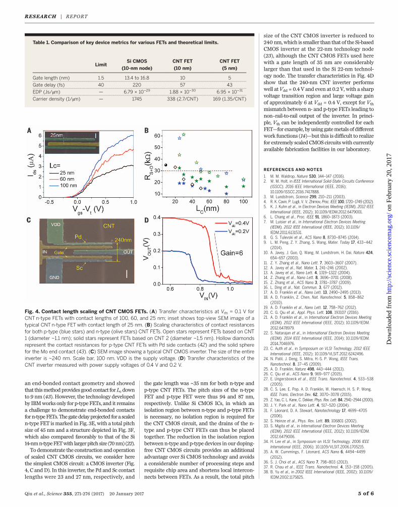
an end-bonded contact geometry and showedthat thismethodprovides good contact forLc downto 9 nm (43). However, the technology developedby IBMworks only for p-type FETs, and it remainsa challenge to demonstrate end-bonded contactsforn-typeFETs. Thegatedelayprojected for a scaledn-type FET ismarked in Fig. 3E, with a total pitchsize of 45 nm and a structure depicted in Fig. 3F,which also compared favorably to that of the Si14-nmn-typeFETwith largerpitch size (70nm) (22).To demonstrate the construction and operation
of scaled CNT CMOS circuits, we consider herethe simplest CMOS circuit: a CMOS inverter (Fig.4, C and D). In this inverter, the Pd and Sc contactlengths were 23 and 27 nm, respectively, and
the gate length was ~35 nm for both n-type andp-type CNT FETs. The pitch sizes of the n-typeFET and p-type FET were thus 94 and 87 nm,respectively. Unlike Si CMOS ICs, in which anisolation region between n-type and p-type FETsis necessary, no isolation region is required forthe CNT CMOS circuit, and the drains of the n-type and p-type CNT FETs can thus be placedtogether. The reduction in the isolation regionbetween n-type and p-type devices in our doping-free CNT CMOS circuits provides an additionaladvantage over Si CMOS technology and avoidsa considerable number of processing steps andrequisite chip area and shortens local intercon-nects between FETs. As a result, the total pitch
size of the CNT CMOS inverter is reduced to240 nm,which is smaller than that of the Si-basedCMOS inverter at the 22-nm technology node(23), although the CNT CMOS FETs used herewith a gate length of 35 nm are considerablylarger than that used in the Si 22-nm technol-ogy node. The transfer characteristics in Fig. 4Dshow that the 240-nm CNT inverter performswell atVdd = 0.4 V and even at 0.2 V, with a sharpvoltage transition region and large voltage gainof approximately 6 at Vdd = 0.4 V, except for Vth
mismatch between n- and p-type FETs leading tonon–rail-to-rail output of the inverter. In princi-ple, Vth can be independently controlled for eachFET—for example, by using gatemetals of differentwork functions (14)—but this is difficult to realizefor extremely scaled CMOS circuitswith currentlyavailable fabrication facilities in our laboratory.
REFERENCES AND NOTES
1. M. M. Waldrop, Nature 530, 144–147 (2016).2. W. M. Holt, in IEEE International Solid-State Circuits Conference
(ISSCC), 2016 IEEE International (IEEE, 2016);10.1109/ISSCC.2016.7417888.
3. M. Lundstrom, Science 299, 210–211 (2003).4. R. K. Cavin, P. Lugli, V. V. Zhirnov, Proc. IEEE 100, 1720–1749 (2012).5. K. J. Kuhn et al., in Electron Devices Meeting (IEDM), 2012 IEEE
International (IEEE, 2012); 10.1109/IEDM.2012.6479001.6. L. Chang et al., Proc. IEEE 91, 1860–1873 (2003).7. M. Luisier et al., in International Electron Devices Meeting
(IEDM), 2012 IEEE International (IEEE, 2012); 10.1109/IEDM.2011.6131531.
8. G. S. Tulevski et al., ACS Nano 8, 8730–8745 (2014).9. L. M. Peng, Z. Y. Zhang, S. Wang, Mater. Today 17, 433–442
(2014).10. A. Javey, J. Guo, Q. Wang, M. Lundstrom, H. Dai, Nature 424,
654–657 (2003).11. Z. Y. Zhang et al., Nano Lett. 7, 3603–3607 (2007).12. A. Javey et al., Nat. Mater. 1, 241–246 (2002).13. A. Javey et al., Nano Lett. 4, 1319–1322 (2004).14. Z. Zhang et al., Nano Lett. 8, 3696–3701 (2008).15. Z. Zhang et al., ACS Nano 3, 3781–3787 (2009).16. L. Ding et al., Nat. Commun. 3, 677 (2012).17. A. D. Franklin et al., Nano Lett. 13, 2490–2495 (2013).18. A. D. Franklin, Z. Chen, Nat. Nanotechnol. 5, 858–862
(2010).19. A. D. Franklin et al., Nano Lett. 12, 758–762 (2012).20. C. G. Qiu et al., Appl. Phys. Lett. 108, 193107 (2016).21. A. D. Franklin et al., in International Electron Devices Meeting
(IEDM), 2012 IEEE International (IEEE, 2012); 10.1109/IEDM.2012.6478979.
22. S. Natarajan et al., in International Electron Devices Meeting(IEDM), 2014 IEEE International (IEEE, 2014); 10.1109/IEDM.2014.7046976.
23. C. Auth et al., in Symposium on VLSI Technology, 2012 IEEEInternational (IEEE, 2012); 10.1109/VLSIT.2012.6242496.
24. N. Patil, J. Deng, S. Mitra, H.-S. P. Wong, IEEE Trans.Nanotechnol. 8, 37–45 (2009).
25. A. D. Franklin, Nature 498, 443–444 (2013).26. C. Qiu et al., ACS Nano 9, 969–977 (2015).27. E. Ungersboeck et al., IEEE Trans. Nanotechnol. 4, 533–538
(2005).28. C. S. Lee, E. Pop, A. D. Franklin, W. Haensch, H. S. P. Wong,
IEEE Trans. Electron Dev. 62, 3070–3078 (2015).29. Z. Yao, C. L. Kane, C. Dekker, Phys. Rev. Lett. 84, 2941–2944 (2000).30. J. Y. Park et al., Nano Lett. 4, 517–520 (2004).31. F. Léonard, D. A. Stewart, Nanotechnology 17, 4699–4705
(2006).32. S. Heinze et al., Phys. Rev. Lett. 89, 106801 (2002).33. S. Migita et al., in International Electron Devices Meeting
(IEDM), 2012 IEEE International (IEEE, 2012); 10.1109/IEDM.2012.6479006.
34. H. Lee et al., in Symposium on VLSI Technology, 2006 IEEEInternational (IEEE, 2006); 10.1109/VLSIT.2006.1705215.
35. A. W. Cummings, F. Léonard, ACS Nano 6, 4494–4499(2012).
36. S. J. Choi et al., ACS Nano 7, 798–803 (2013).37. R. Chau et al., IEEE Trans. Nanotechnol. 4, 153–158 (2005).38. B. Yu et al., in 2002 IEEE International (IEEE, 2002); 10.1109/
IEDM.2002.1175825.
Qiu et al., Science 355, 271-276 (2017) 20 January 2017 5 of 6
Table 1. Comparison of key device metrics for various FETs and theoretical limits.
LimitSi CMOS
(10-nm node)
CNT FET
(10 nm)
CNT FET
(5 nm)
Gate length (nm) 1.5 13.4 to 16.8 10 5.. .. ... ... .. ... .. ... ... .. ... ... .. ... .. ... ... .. ... ... .. ... ... .. ... .. ... ... .. ... ... .. ... .. ... ... .. ... ... .. ... ... .. ... .. ... ... .. ... ... .. ... .. ... ... .. ... ... .. ... ... .. ... .. ... ... .. ... ... .. ... .. ... ... .. ... ... .. ... ... .. .
Gate delay (fs) 40 220 57 43.. .. ... ... .. ... .. ... ... .. ... ... .. ... .. ... ... .. ... ... .. ... ... .. ... .. ... ... .. ... ... .. ... .. ... ... .. ... ... .. ... ... .. ... .. ... ... .. ... ... .. ... .. ... ... .. ... ... .. ... ... .. ... .. ... ... .. ... ... .. ... .. ... ... .. ... ... .. ... ... .. .
EDP (Js/mm) — 6.79 × 10⁻²⁹ 1.88 × 10⁻³⁰ 6.95 × 10⁻³¹.. .. ... ... .. ... .. ... ... .. ... ... .. ... .. ... ... .. ... ... .. ... ... .. ... .. ... ... .. ... ... .. ... .. ... ... .. ... ... .. ... ... .. ... .. ... ... .. ... ... .. ... .. ... ... .. ... ... .. ... ... .. ... .. ... ... .. ... ... .. ... .. ... ... .. ... ... .. ... ... .. .
Carrier density (1/mm) — 1745 338 (2.7/CNT) 169 (1.35/CNT).. .. ... ... .. ... .. ... ... .. ... ... .. ... .. ... ... .. ... ... .. ... ... .. ... .. ... ... .. ... ... .. ... .. ... ... .. ... ... .. ... ... .. ... .. ... ... .. ... ... .. ... .. ... ... .. ... ... .. ... ... .. ... .. ... ... .. ... ... .. ... .. ... ... .. ... ... .. ... ... .. .
Fig. 4. Contact length scaling of CNT CMOS FETs. (A) Transfer characteristics at Vds = 0.1 V forCNT n-type FETs with contact lengths of 100, 60, and 25 nm; inset shows top-view SEM image of atypical CNTn-type FETwith contact length of 25 nm. (B) Scaling characteristics of contact resistancesfor both p-type (blue stars) and n-type (olive stars) CNT FETs. Open stars represent FETs based on CNT1 (diameter ~1.1 nm); solid stars represent FETs based on CNT 2 (diameter ~1.5 nm). Hollow diamondsrepresent the contact resistances for p-type CNT FETs with Pd side contacts (42) and the solid spherefor the Mo end contact (43). (C) SEM image showing a typical CNT CMOS inverter.The size of the entireinverter is ~240 nm. Scale bar, 100 nm. VDD is the supply voltage. (D) Transfer characteristics of theCNT inverter measured with power supply voltages of 0.4 V and 0.2 V.
RESEARCH | REPORT
on
Febr
uary
20,
201
7ht
tp://
scie
nce.
scie
ncem
ag.o
rg/
Dow
nloa
ded
from
39. International Technology Roadmap for Semiconductors (2013edition); www.itrs2.net/2013-itrs.html.
40. W. Haensch et al., IBM J. Res. Develop. 50, 339–361 (2006).41. J. D. Meindl, Q. Chen, J. A. Davis, Science 293, 2044–2049 (2001).42. A. D. Franklin, D. B. Farmer, W. Haensch, ACS Nano 8,
7333–7339 (2014).43. Q. Cao et al., Science 350, 68–72 (2015).
ACKNOWLEDGMENTS
We thank J. Su, Y. Gao, and L. Ding from Huazhong University ofScience and Technology for TEM technique support; H. Peng and
B. Deng from Peking University for supplying CVD-derivedgraphene samples; and Y. Wu and G. Zhang for useful discussions.Supported by National Key Research and Development Programgrants 2016YFA0201901 and 2016YFA0201902; National ScienceFoundation of China grants 61322105, 61376126, 61621001, and61427901; and Beijing Municipal Science and TechnologyCommission grants D151100003315004 and Z151100003315009.Author contributions: L.-M.P. and Z.Z. proposed and supervised theproject; Z.Z. and L.-M.P. designed the experiment; C.Q. and Y.Y.performed the device fabrication and characterization; C.Q., M.X.,and D.Z. grew the nanotubes; and Z.Z., C.Q., and L.-M.P. analyzed
the data and co-wrote the manuscript. All the authors discussedthe results and commented on the manuscript.
SUPPLEMENTARY MATERIALS
www.sciencemag.org/content/355/6322/271/suppl/DC1Materials and MethodsFigs. S1 to S15References (44–47)
6 September 2016; accepted 21 December 201610.1126/science.aaj1628
Qiu et al., Science 355, 271-276 (2017) 20 January 2017 6 of 6
RESEARCH | REPORT
on
Febr
uary
20,
201
7ht
tp://
scie
nce.
scie
ncem
ag.o
rg/
Dow
nloa
ded
from

(6322), 271-276. [doi: 10.1126/science.aaj1628]355Science Donglai Zhong and Lian-Mao Peng (January 19, 2017) Chenguang Qiu, Zhiyong Zhang, Mengmeng Xiao, Yingjun Yang,gate lengthsScaling carbon nanotube complementary transistors to 5-nm
Editor's Summary
, this issue p. 271Sciencesupply voltage, and they approached the limit of one electron per switching operation.with silicon CMOS devices, the nanotube-based devices operated much faster and at much lowergraphene contacts helped maintain electrostatic control. A scaling trend study revealed that, compared
fabricated top-gated carbon nanotube field-effect transistors with a gate length of 5 nm. Thinet al.Qiu (CMOS) devices based on silicon technology is to use semiconducting carbon nanotubes as the gates.
One option for extending the performance of complementary metal-oxide semiconductorMoving transistors downscale
This copy is for your personal, non-commercial use only.
Article Tools
http://science.sciencemag.org/content/355/6322/271article tools: Visit the online version of this article to access the personalization and
Permissionshttp://www.sciencemag.org/about/permissions.dtlObtain information about reproducing this article:
is a registered trademark of AAAS. ScienceAdvancement of Science; all rights reserved. The title Avenue NW, Washington, DC 20005. Copyright 2016 by the American Association for thein December, by the American Association for the Advancement of Science, 1200 New York
(print ISSN 0036-8075; online ISSN 1095-9203) is published weekly, except the last weekScience
on
Febr
uary
20,
201
7ht
tp://
scie
nce.
scie
ncem
ag.o
rg/
Dow
nloa
ded
from