Embed Size (px)
Citation preview
Carbon Nanotube Field-Effect Transistors (CNTFETs): Evolution and Applications
for Future Nanoscale ICs
Tamer Ragheb
ELEC 527 Presentation
Rice University
3/15/2007
2/37
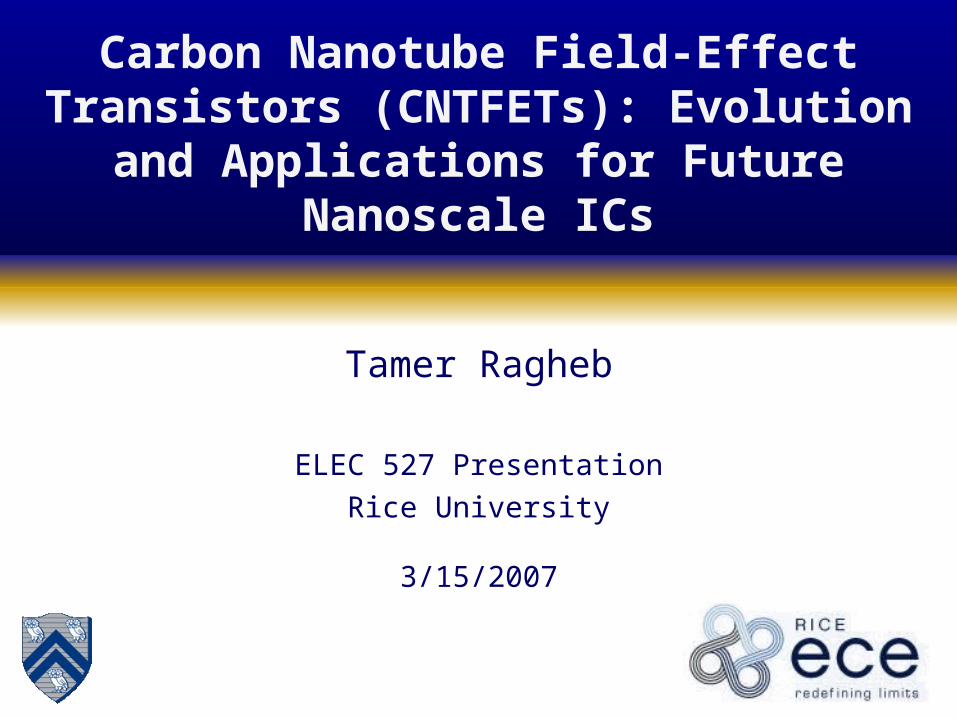
Conventional Semiconductor Microelectronics Will Come to an End
Conventional semiconductor device scaling obstacles: Diffusion areas will no longer be
separated by a low doped channel region
Equivalent gate oxide thickness will fall below the tunneling limit
Lithography costs will increase exponentially
Solution:Find new technologies such as
molecular electronics and CNT
Lateral Scaling
Vertical Scaling
Hoenlein et al., Materials Science and Engineering: C, 2003
3/37
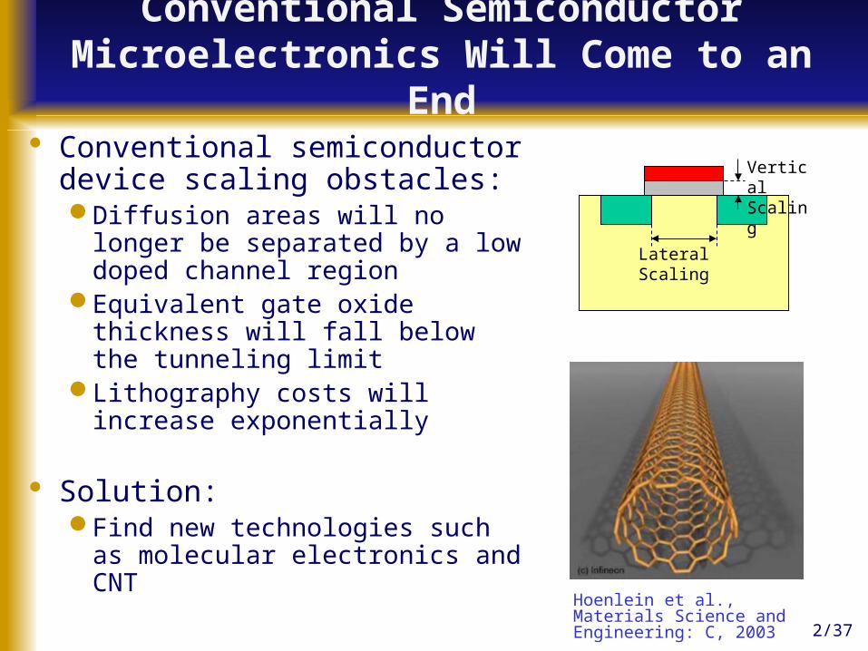
Why Carbon Nanotubes (CNTs)?
CNTs exhibit remarkable electronic and mechanical characteristics due to:Extraordinary strength of the carbon-carbon bondThe small atomic diameter of the carbon atomThe availability of free π-electrons in the graphitic
configuration
Hoenlein et al., Materials Science and Engineering: C, vol. 23, no. 8, pp. 663-669, 2003
4/37
Carbon Nanotube Field-Effect Transistors (CNTFETs): Evolution
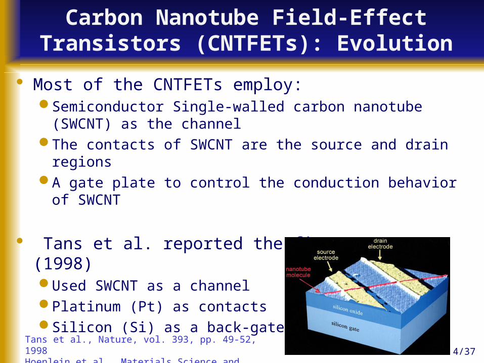
Most of the CNTFETs employ:Semiconductor Single-walled carbon nanotube (SWCNT)
as the channelThe contacts of SWCNT are the source and drain regionsA gate plate to control the conduction behavior of SWCNT
Tans et al. reported the first CNTFET (1998)Used SWCNT as a channelPlatinum (Pt) as contactsSilicon (Si) as a back-gate
Tans et al., Nature, vol. 393, pp. 49-52, 1998Hoenlein et al., Materials Science and Engineering: C, 2003
5/37
Carbon Nanotube Field-Effect Transistors (CNTFETs): Evolution
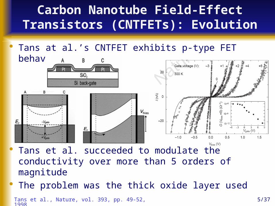
Tans at al.’s CNTFET exhibits p-type FET behavior
Tans et al. succeeded to modulate the conductivity over more than 5 orders of magnitude
The problem was the thick oxide layer used Tans et al., Nature, vol. 393, pp. 49-52, 1998
6/37
Carbon Nanotube Field-Effect Transistors (CNTFETs): Evolution
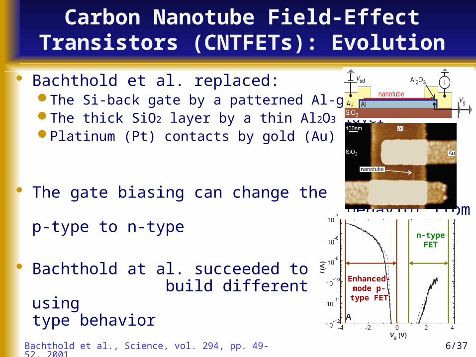
Bachthold et al. replaced:The Si-back gate by a patterned Al-gateThe thick SiO2 layer by a thin Al2O3 layerPlatinum (Pt) contacts by gold (Au)
The gate biasing can change the behavior from p-type to n-type
Bachthold at al. succeeded to build different logic gates using the p-type behavior
Bachthold et al., Science, vol. 294, pp. 49-52, 2001
Enhanced-mode p-type
FET
n-type FET
7/37
Carbon Nanotube Field-Effect Transistors (CNTFETs): Evolution
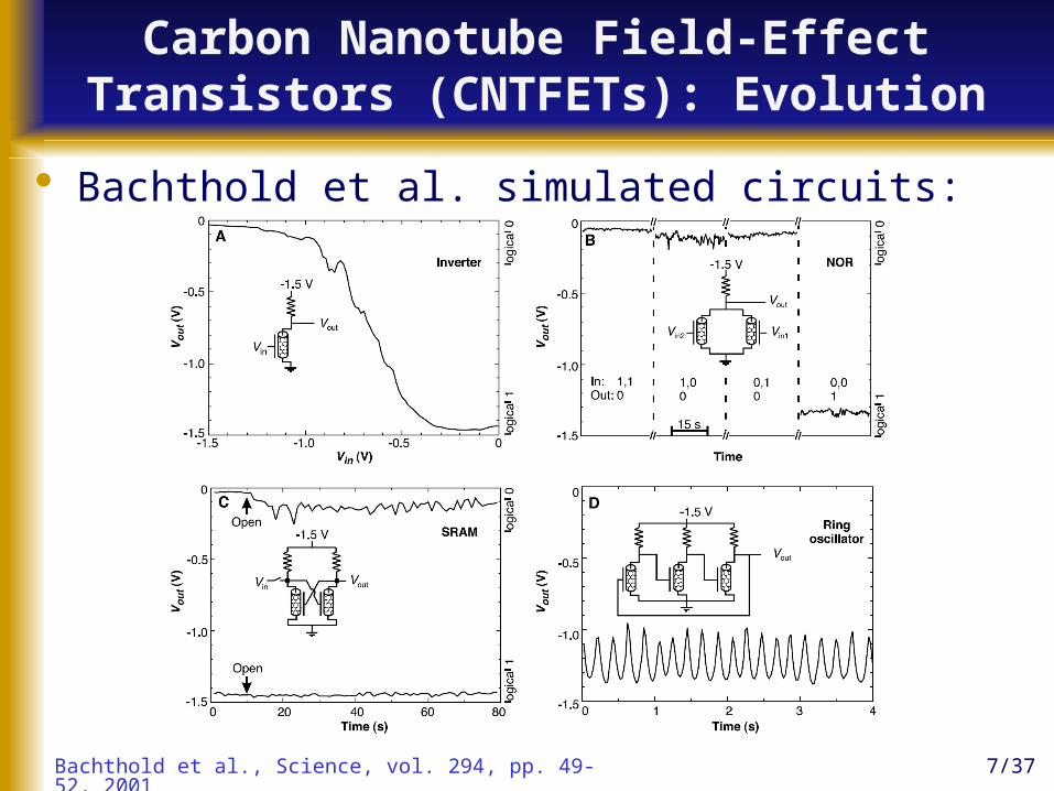
Bachthold et al. simulated circuits:
Bachthold et al., Science, vol. 294, pp. 49-52, 2001
8/37
Carbon Nanotube Field-Effect Transistors (CNTFETs): Evolution
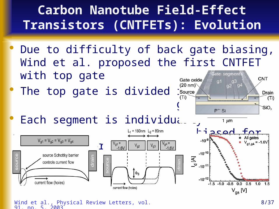
Due to difficulty of back gate biasing, Wind et al. proposed the first CNTFET with top gate
The top gate is divided into 4 gate segments
Each segment is individually biased for more behavior control
Wind et al., Physical Review Letters, vol. 91, no. 5, 2003
9/37
Carbon Nanotube Field-Effect Transistors (CNTFETs): Evolution
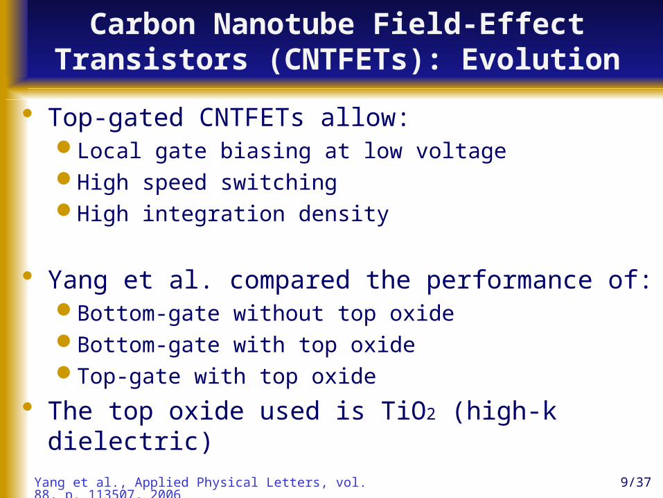
Top-gated CNTFETs allow:Local gate biasing at low voltageHigh speed switchingHigh integration density
Yang et al. compared the performance of:Bottom-gate without top oxideBottom-gate with top oxideTop-gate with top oxide
The top oxide used is TiO2 (high-k dielectric)
Yang et al., Applied Physical Letters, vol. 88, p. 113507, 2006
10/37
Carbon Nanotube Field-Effect Transistors (CNTFETs): Evolution
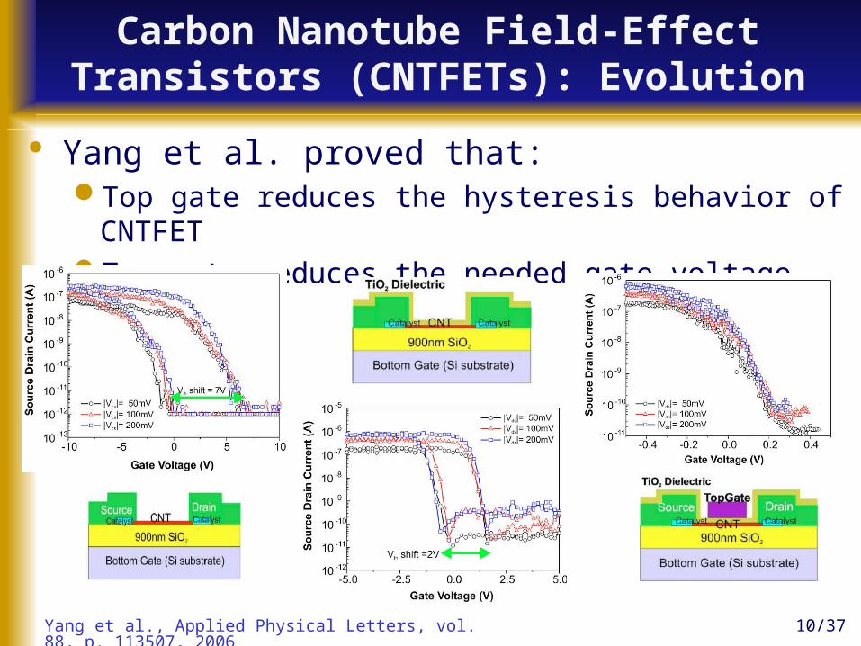
Yang et al. proved that:Top gate reduces the hysteresis behavior of CNTFETTop gate reduces the needed gate voltage
Yang et al., Applied Physical Letters, vol. 88, p. 113507, 2006
11/37
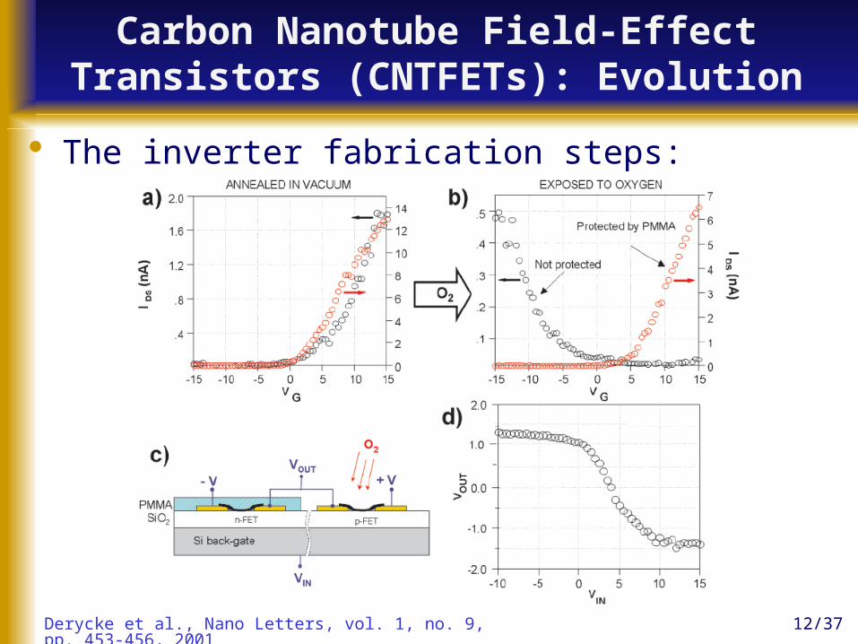
Carbon Nanotube Field-Effect Transistors (CNTFETs): Evolution
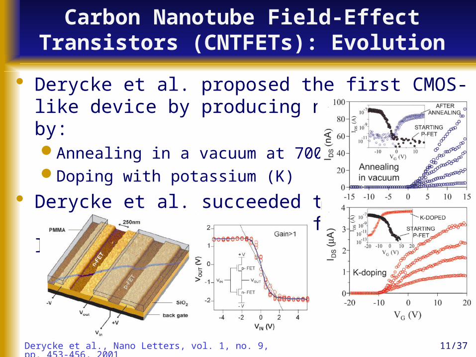
Derycke et al. proposed the first CMOS-like device by producing n-type CNTFETs by:Annealing in a vacuum at 700KDoping with potassium (K)
Derycke et al. succeeded to build the first CMOS-like inverter
Derycke et al., Nano Letters, vol. 1, no. 9, pp. 453-456, 2001
12/37
Carbon Nanotube Field-Effect Transistors (CNTFETs): Evolution
The inverter fabrication steps:
Derycke et al., Nano Letters, vol. 1, no. 9, pp. 453-456, 2001
13/37
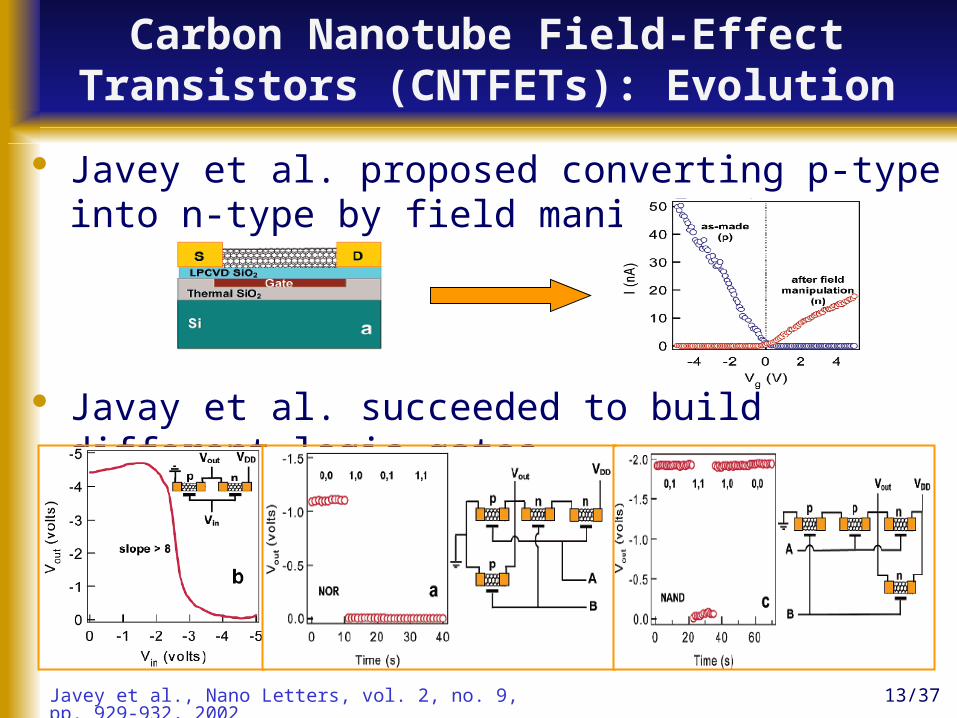
Carbon Nanotube Field-Effect Transistors (CNTFETs): Evolution
Javey et al. proposed converting p-type into n-type by field manipulation
Javay et al. succeeded to build different logic gates
Javey et al., Nano Letters, vol. 2, no. 9, pp. 929-932, 2002
14/37
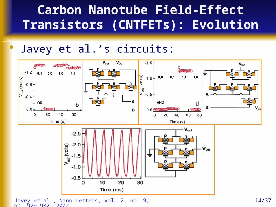
Carbon Nanotube Field-Effect Transistors (CNTFETs): Evolution
Javey et al.’s circuits:
Javey et al., Nano Letters, vol. 2, no. 9, pp. 929-932, 2002

15/37
Carbon Nanotube Field-Effect Transistors (CNTFETs): Evolution
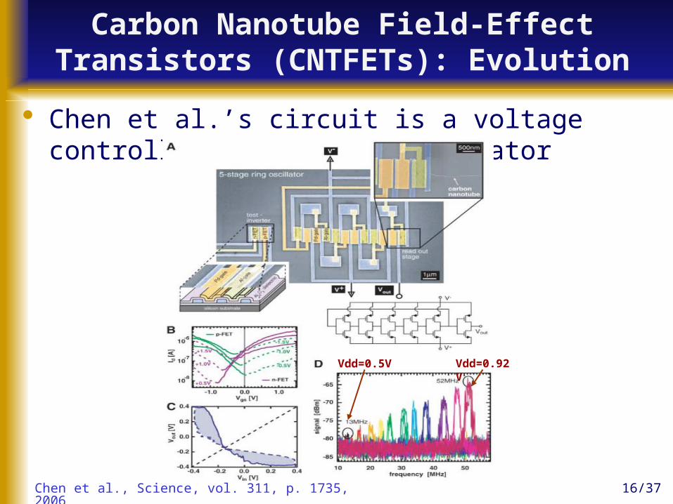
Chen et al. proposed a complete integrated logic circuit assembled on a single CNT
They controlled the polarities of the FETs by using metals with different work functions as the gates
Chen et al., Science, vol. 311, p. 1735, 2006
16/37
Carbon Nanotube Field-Effect Transistors (CNTFETs): Evolution
Chen et al.’s circuit is a voltage controlled (Vdd) ring oscillator
Chen et al., Science, vol. 311, p. 1735, 2006
Vdd=0.92VVdd=0.5V
17/37
Carbon Nanotube Field-Effect Transistors (CNTFETs): Evolution
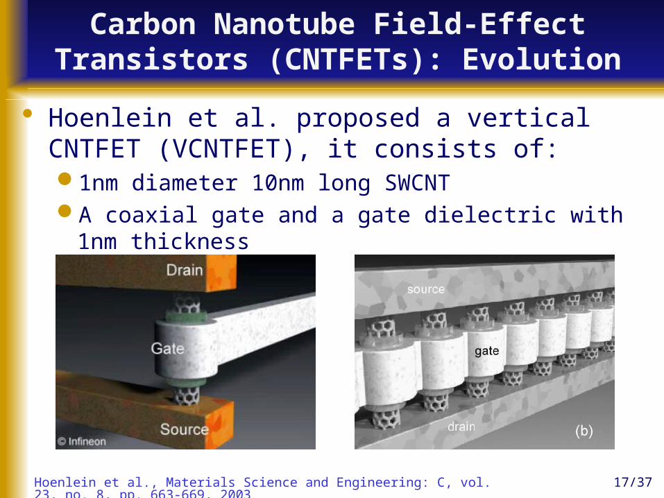
Hoenlein et al. proposed a vertical CNTFET (VCNTFET), it consists of:1nm diameter 10nm long SWCNTA coaxial gate and a gate dielectric with 1nm thickness
Hoenlein et al., Materials Science and Engineering: C, vol. 23, no. 8, pp. 663-669, 2003
18/37
Carbon Nanotube Field-Effect Transistors (CNTFETs): Evolution
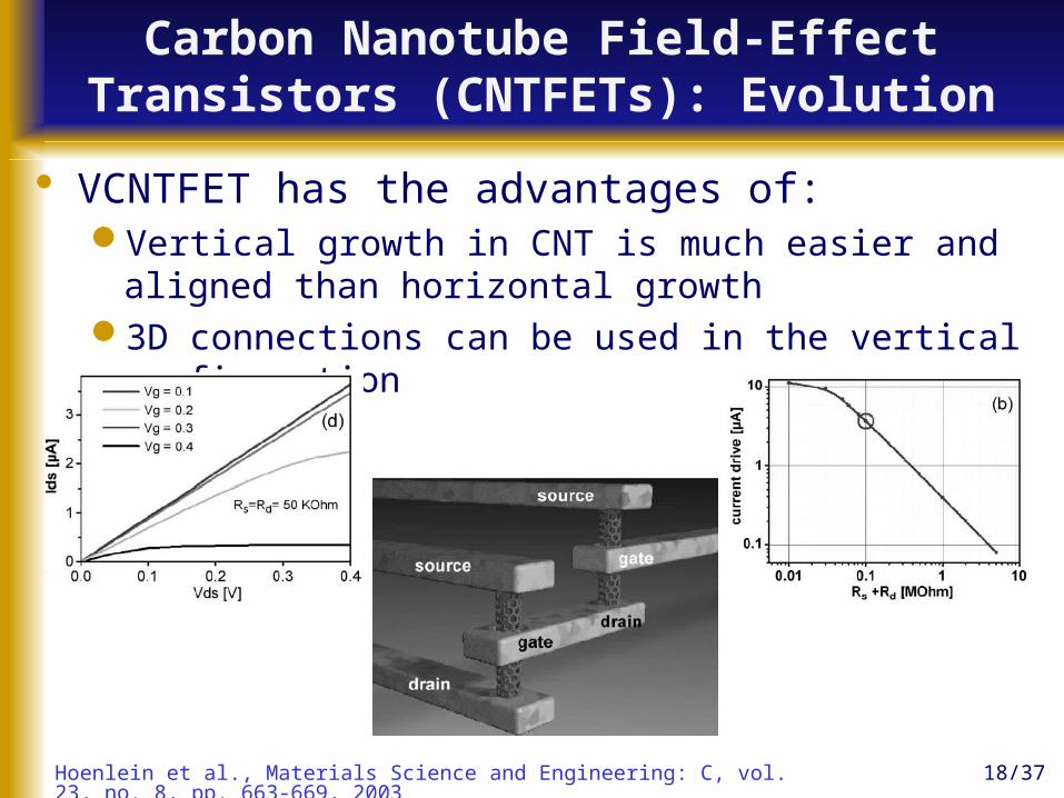
VCNTFET has the advantages of:Vertical growth in CNT is much easier and aligned than
horizontal growth3D connections can be used in the vertical configuration
Hoenlein et al., Materials Science and Engineering: C, vol. 23, no. 8, pp. 663-669, 2003
19/37
Carbon Nanotube Field-Effect Transistors (CNTFETs): Evolution
All the previous structures depend on semiconductor SWCNT.
SWCNT available commercially contain about 33-60% metallic CNTs.
For mass production and high yield, methods have to be found to guarantee that CNTFETs use semiconductor type SWCNTs.
Chen et al. and Na et al. proposed 2 different methods to convert metallic CNTs into semiconductor type.
Chen et al., Japanese Journal of Applied Physics, vol. 45, no. 4B, pp. 3680-3685, 2006Na et al., Fullerenes, Nanotubes, and Carbon Nanostructures, vol. 14, pp. 141-149, 2006
20/37
Carbon Nanotube Field-Effect Transistors (CNTFETs): Evolution
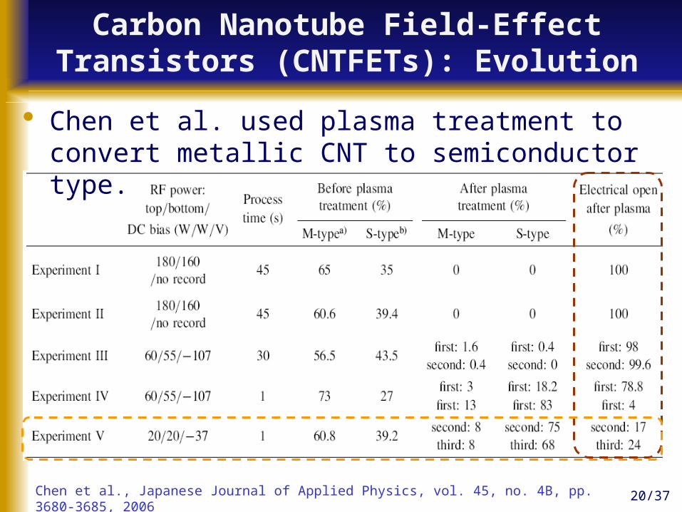
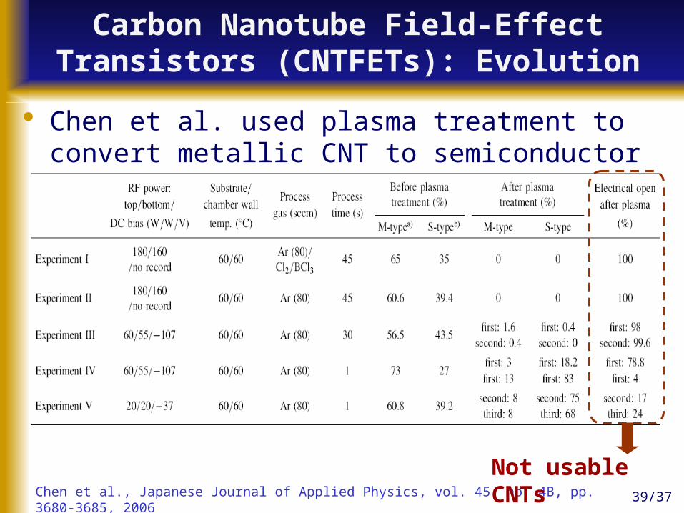
Chen et al. used plasma treatment to convert metallic CNT to semiconductor type.
Chen et al., Japanese Journal of Applied Physics, vol. 45, no. 4B, pp. 3680-3685, 2006
21/37
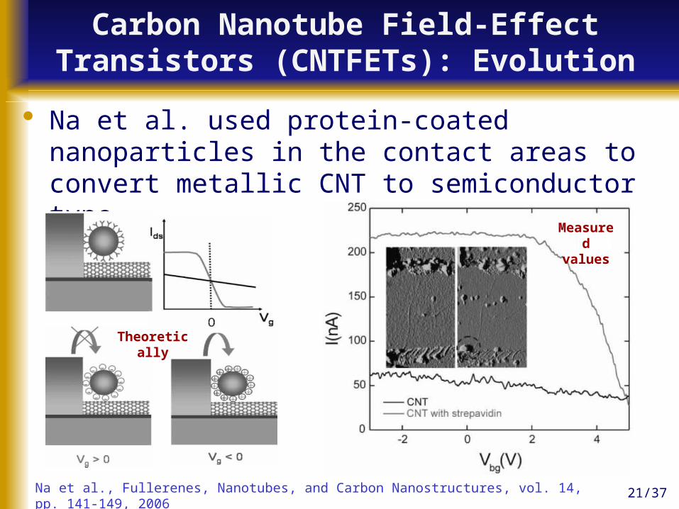
Carbon Nanotube Field-Effect Transistors (CNTFETs): Evolution
Na et al. used protein-coated nanoparticles in the contact areas to convert metallic CNT to semiconductor type.
Na et al., Fullerenes, Nanotubes, and Carbon Nanostructures, vol. 14, pp. 141-149, 2006
Measured values
Theoretically
22/37
Carbon Nanotube Field-Effect Transistors (CNTFETs): Evolution
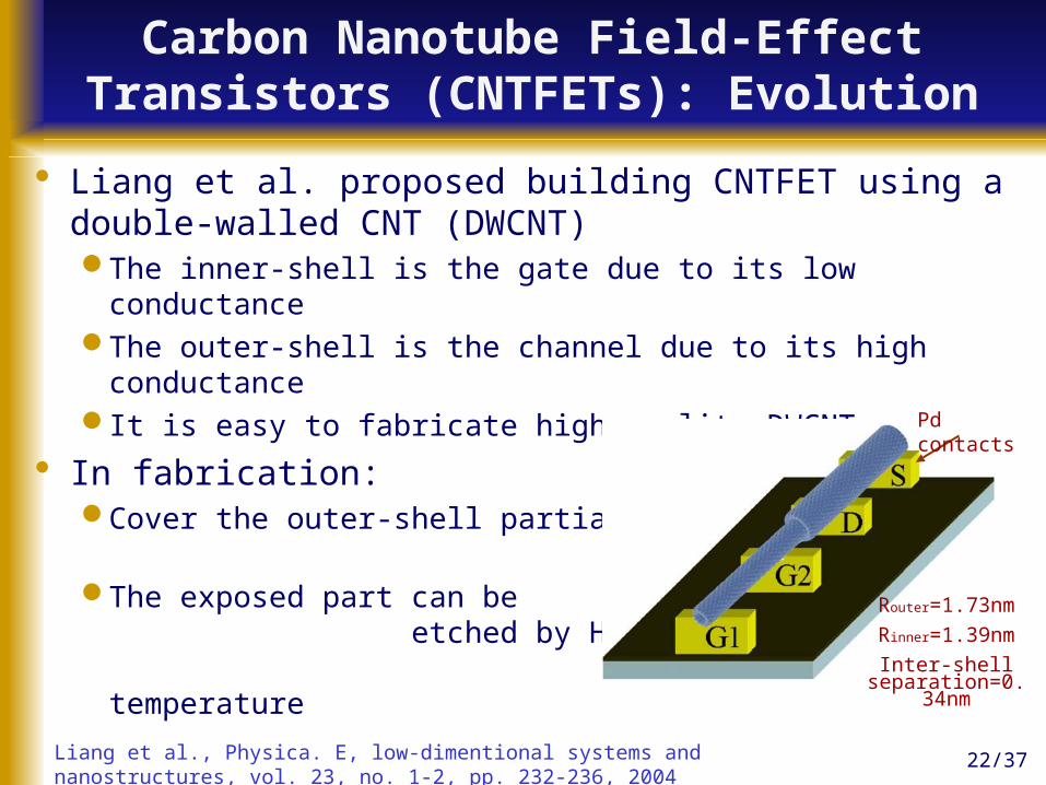
Liang et al. proposed building CNTFET using a double-walled CNT (DWCNT)The inner-shell is the gate due to its low conductanceThe outer-shell is the channel due to its high conductanceIt is easy to fabricate high-quality DWCNT
In fabrication:Cover the outer-shell partially
by polymer-patternsThe exposed part can be
etched by H2O or O2 plasma at room temperature
Liang et al., Physica. E, low-dimentional systems and nanostructures, vol. 23, no. 1-2, pp. 232-236, 2004
Router=1.73nm
Rinner=1.39nm
Inter-shell separation=0.34nm
Pd contacts
23/37
Carbon Nanotube Field-Effect Transistors (CNTFETs): Evolution
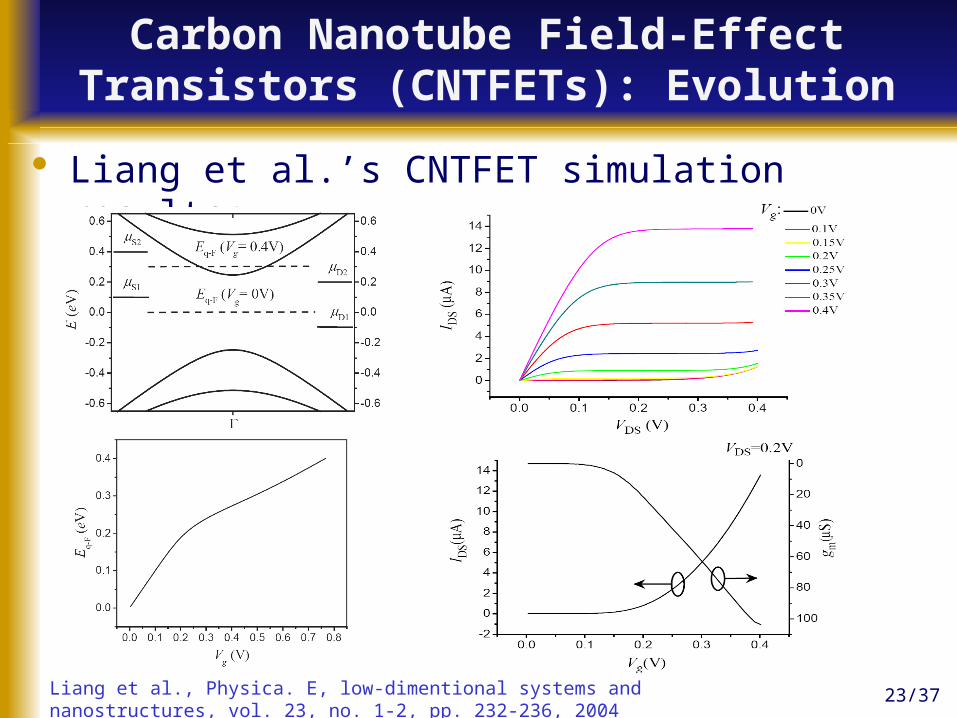
Liang et al.’s CNTFET simulation results:
Liang et al., Physica. E, low-dimentional systems and nanostructures, vol. 23, no. 1-2, pp. 232-236, 2004
24/37
CNTFET as Memory Devices
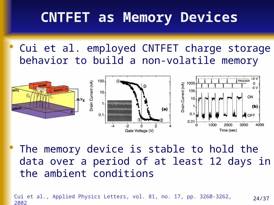
Cui et al. employed CNTFET charge storage behavior to build a non-volatile memory
The memory device is stable to hold the data over a period of at least 12 days in the ambient conditions
Cui et al., Applied Physics Letters, vol. 81, no. 17, pp. 3260-3262, 2002
25/37
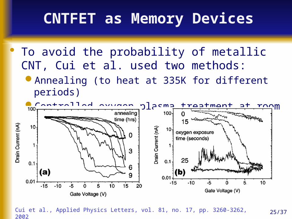
CNTFET as Memory Devices
To avoid the probability of metallic CNT, Cui et al. used two methods:Annealing (to heat at 335K for different periods)Controlled oxygen plasma treatment at room temperature
Cui et al., Applied Physics Letters, vol. 81, no. 17, pp. 3260-3262, 2002
26/37
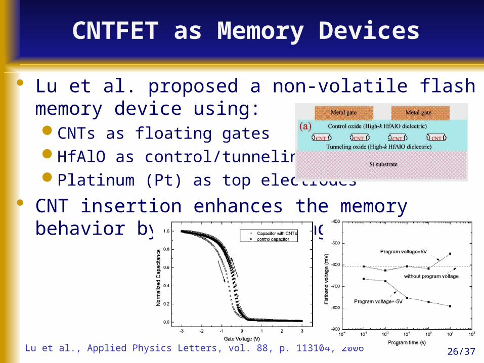
CNTFET as Memory Devices
Lu et al. proposed a non-volatile flash memory device using:CNTs as floating gatesHfAlO as control/tunneling oxidePlatinum (Pt) as top electrodes
CNT insertion enhances the memory behavior by holes trapping
Lu et al., Applied Physics Letters, vol. 88, p. 113104, 2006
27/37
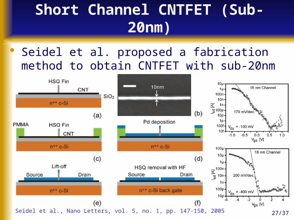
Short Channel CNTFET (Sub-20nm)
Seidel et al. proposed a fabrication method to obtain CNTFET with sub-20nm long channels
Seidel et al., Nano Letters, vol. 5, no. 1, pp. 147-150, 2005
28/37
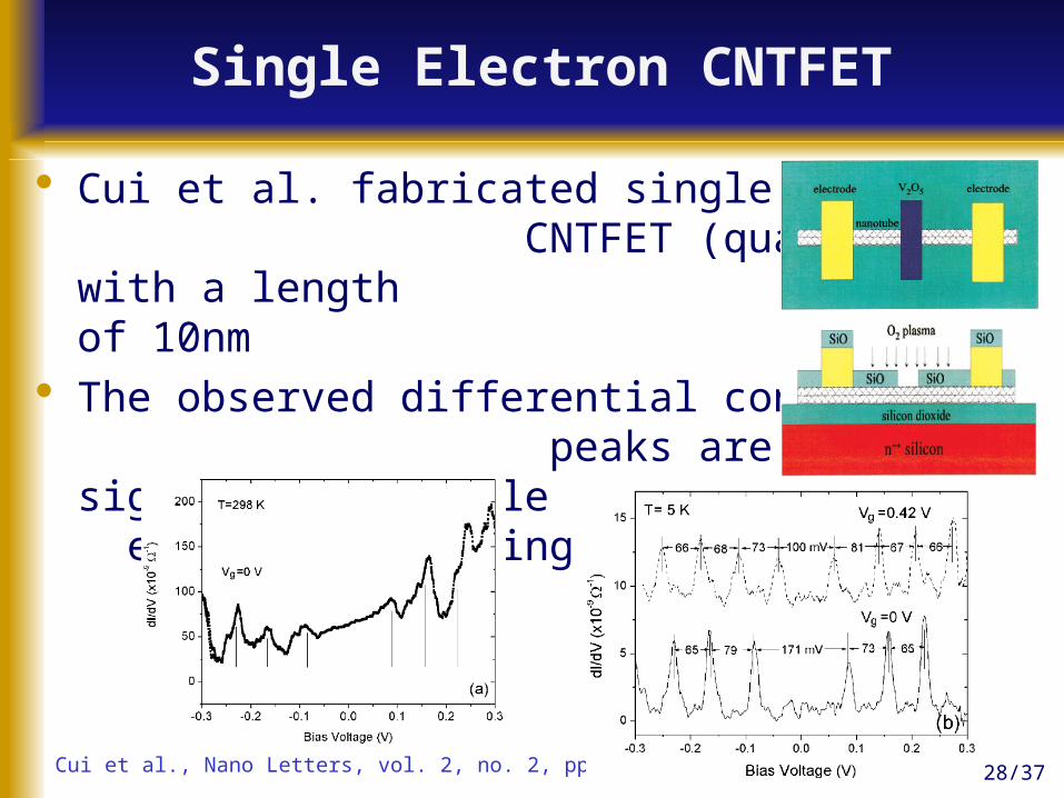
Single Electron CNTFET
Cui et al. fabricated single electron CNTFET (quantum dot) with a length of 10nm
The observed differential conductance peaks are a clear signature of single electron tunneling in the device
Cui et al., Nano Letters, vol. 2, no. 2, pp. 117-120, 2002
29/37
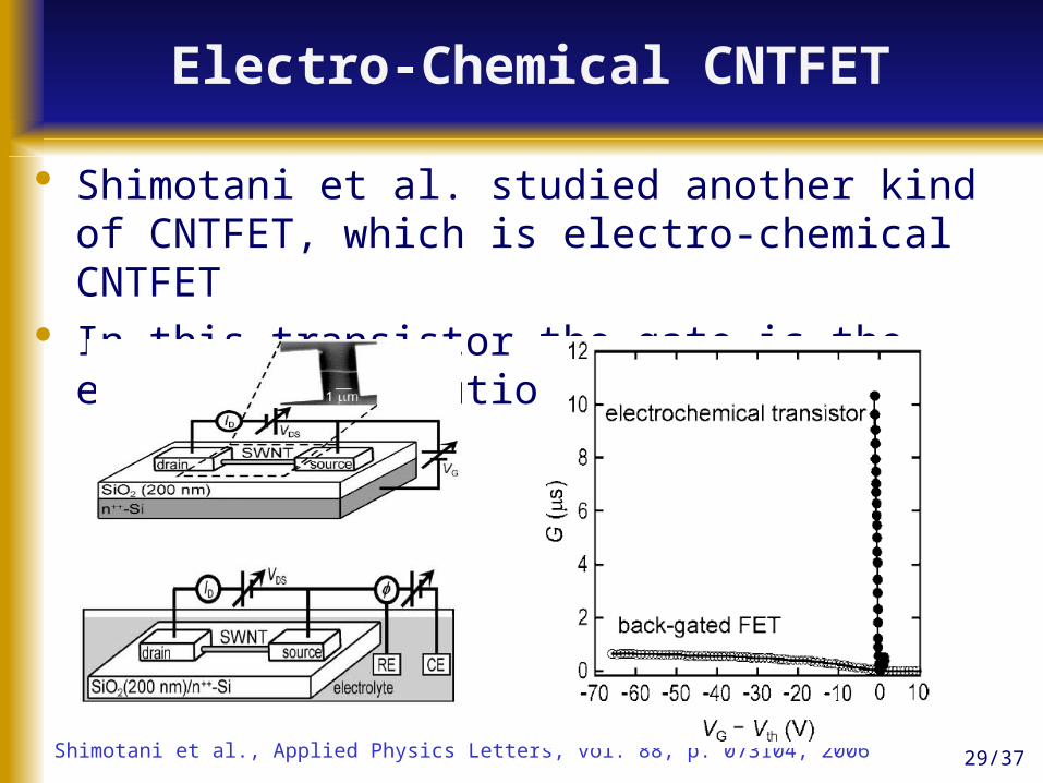
Electro-Chemical CNTFET
Shimotani et al. studied another kind of CNTFET, which is electro-chemical CNTFET
In this transistor the gate is the electrolyte solution
Shimotani et al., Applied Physics Letters, vol. 88, p. 073104, 2006
30/37
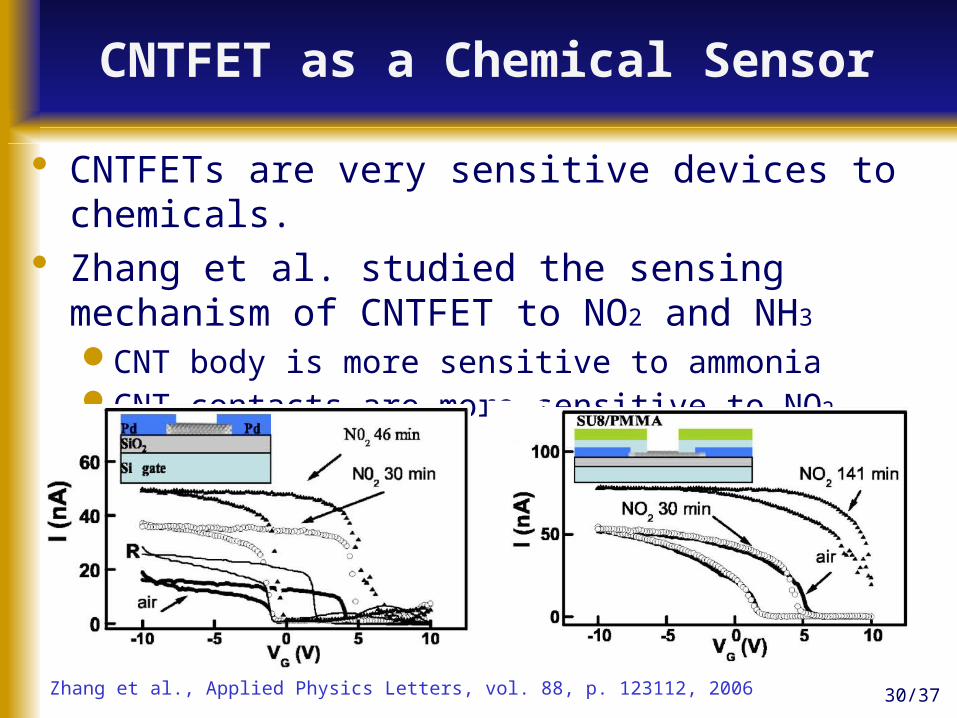
CNTFET as a Chemical Sensor
CNTFETs are very sensitive devices to chemicals. Zhang et al. studied the sensing mechanism of
CNTFET to NO2 and NH3 CNT body is more sensitive to ammoniaCNT contacts are more sensitive to NO2
Zhang et al., Applied Physics Letters, vol. 88, p. 123112, 2006
31/37
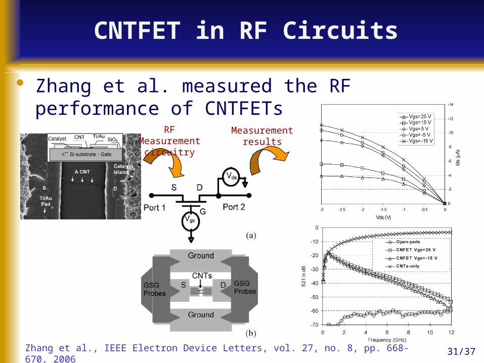
CNTFET in RF Circuits
Zhang et al. measured the RF performance of CNTFETs
Zhang et al., IEEE Electron Device Letters, vol. 27, no. 8, pp. 668-670, 2006
RF Measurement circuitry
Measurement results
32/37
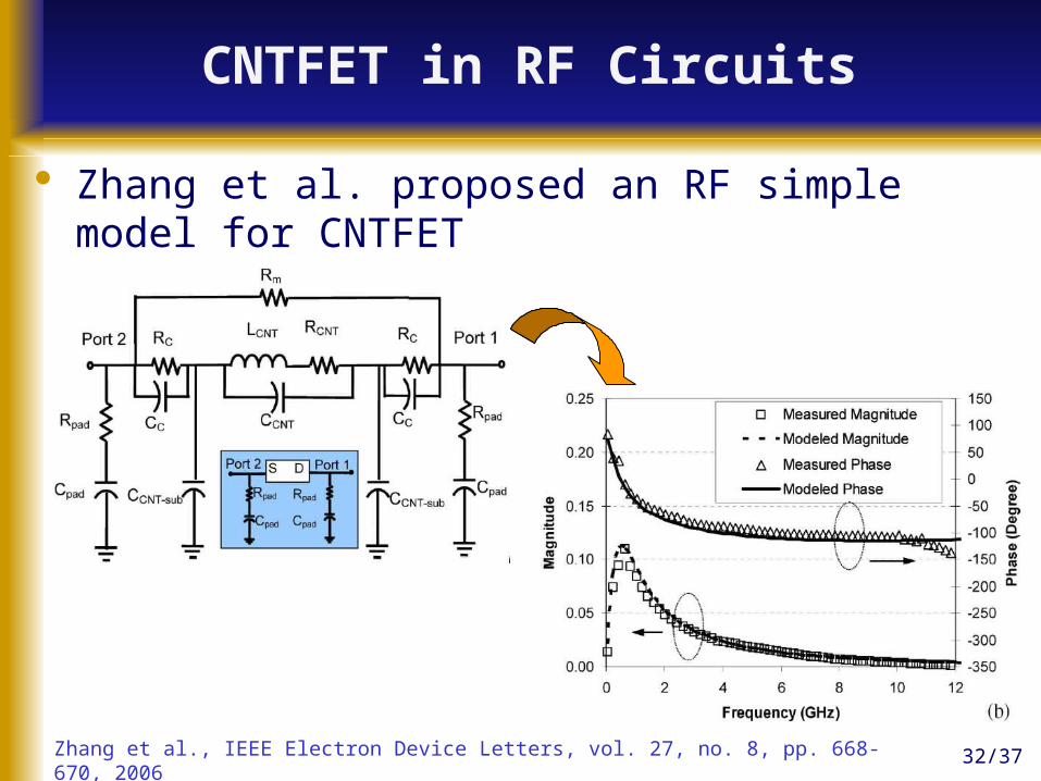
CNTFET in RF Circuits
Zhang et al. proposed an RF simple model for CNTFET
Zhang et al., IEEE Electron Device Letters, vol. 27, no. 8, pp. 668-670, 2006
33/37
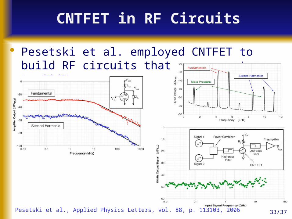
CNTFET in RF Circuits
Pesetski et al. employed CNTFET to build RF circuits that can operate up to 23GHz
Pesetski et al., Applied Physics Letters, vol. 88, p. 113103, 2006
34/37
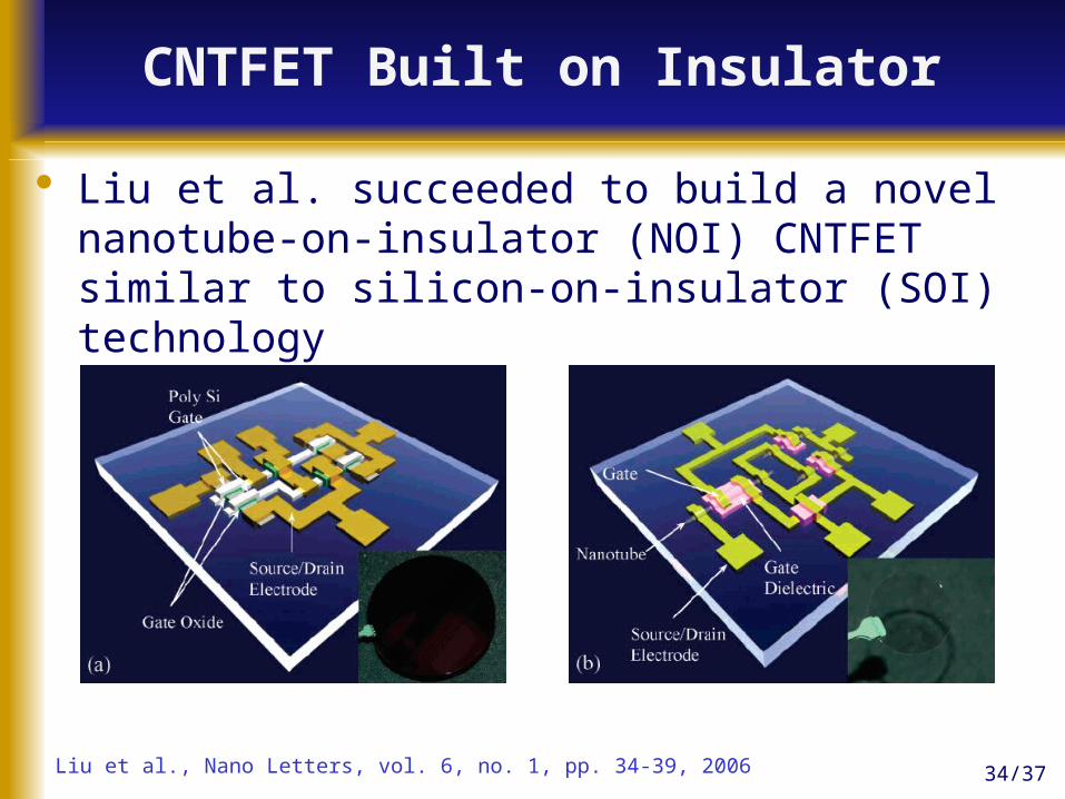
CNTFET Built on Insulator
Liu et al. succeeded to build a novel nanotube-on-insulator (NOI) CNTFET similar to silicon-on-insulator (SOI) technology
Liu et al., Nano Letters, vol. 6, no. 1, pp. 34-39, 2006
35/37
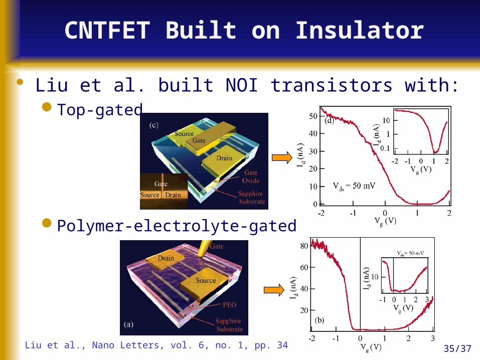
CNTFET Built on Insulator
Liu et al. built NOI transistors with:Top-gated
Polymer-electrolyte-gated
Liu et al., Nano Letters, vol. 6, no. 1, pp. 34-39, 2006
36/37
Conclusions
CNT is a future replacement for semiconductor based microelectronics
The evolution of CNTFET is discussed Employing CNTFET in a lot of applications such as:
Logic circuitsMemoriesChemical sensorsRF circuits
Integrating CNT based interconnects with devices can produce a complete future nanoscale ICs
37/37
References (in Order of Appearance)
Hoenlein et al., Materials Science and Engineering: C, vol. 23, no. 8, pp. 663-669, 2003 Tans et al., Nature, vol. 393, pp. 49-52, 1998 Bachthold et al., Science, vol. 294, pp. 49-52, 2001 Wind et al., Physical Review Letters, vol. 91, no. 5, 2003 Yang et al., Applied Physical Letters, vol. 88, p. 113507, 2006 Derycke et al., Nano Letters, vol. 1, no. 9, pp. 453-456, 2001 Javey et al., Nano Letters, vol. 2, no. 9, pp. 929-932, 2002 Chen et al., Science, vol. 311, p. 1735, 2006 Chen et al., Japanese Journal of Applied Physics, vol. 45, no. 4B, pp. 3680-3685, 2006 Na et al., Fullerenes, Nanotubes, and Carbon Nanostructures, vol. 14, pp. 141-149, 2006 Liang et al., Physica. E, low-dimentional systems and nanostructures, vol. 23, no. 1-2, pp.
232-236, 2004 Cui et al., Applied Physics Letters, vol. 81, no. 17, pp. 3260-3262, 2002 Lu et al., Applied Physics Letters, vol. 88, p. 113104, 2006 Seidel et al., Nano Letters, vol. 5, no. 1, pp. 147-150, 2005 Cui et al., Nano Letters, vol. 2, no. 2, pp. 117-120, 2002 Shimotani et al., Applied Physics Letters, vol. 88, p. 073104, 2006 Zhang et al., Applied Physics Letters, vol. 88, p. 123112, 2006 Pesetski et al., Applied Physics Letters, vol. 88, p. 113103, 2006 Liu et al., Nano Letters, vol. 6, no. 1, pp. 34-39, 2006
Thank You
Acknowledgments:Prof. James M. Tour and Prof. Lin Zhong
Colleagues in RAND group
Colleagues in the ELEC 527 class
39/37
Carbon Nanotube Field-Effect Transistors (CNTFETs): Evolution
Chen et al. used plasma treatment to convert metallic CNT to semiconductor type.
Chen et al., Japanese Journal of Applied Physics, vol. 45, no. 4B, pp. 3680-3685, 2006
Not usable CNTs


![Dr. Eng. Tamer Farouk M. A. Khalifa · Dr. Tamer F. Khalifa CV [1028] Dr. Tamer Farouk Khalifa – tamerkhalifa@hotmail.com tamer.farouk@buc.edu.eg Page 2 Editorial board of Journal](https://img.pdfslide.us/doc/110x75/5e291dbd14c5ff1a88709d12/dr-eng-tamer-farouk-m-a-khalifa-dr-tamer-f-khalifa-cv-1028-dr-tamer-farouk.jpg)