Embed Size (px)
Citation preview

To learn more about ON Semiconductor, please visit our website at www.onsemi.com
Is Now Part of
ON Semiconductor and the ON Semiconductor logo are trademarks of Semiconductor Components Industries, LLC dba ON Semiconductor or its subsidiaries in the United States and/or other countries. ON Semiconductor owns the rights to a number of patents, trademarks, copyrights, trade secrets, and other intellectual property. A listing of ON Semiconductor’s product/patent coverage may be accessed at www.onsemi.com/site/pdf/Patent-Marking.pdf. ON Semiconductor reserves the right to make changes without further notice to any products herein. ON Semiconductor makes no warranty, representation or guarantee regarding the suitability of its products for any particular purpose, nor does ON Semiconductor assume any liability arising out of the application or use of any product or circuit, and specifically disclaims any and all liability, including without limitation special, consequential or incidental damages. Buyer is responsible for its products and applications using ON Semiconductor products, including compliance with all laws, regulations and safety requirements or standards, regardless of any support or applications information provided by ON Semiconductor. “Typical” parameters which may be provided in ON Semiconductor data sheets and/or specifications can and do vary in different applications and actual performance may vary over time. All operating parameters, including “Typicals” must be validated for each customer application by customer’s technical experts. ON Semiconductor does not convey any license under its patent rights nor the rights of others. ON Semiconductor products are not designed, intended, or authorized for use as a critical component in life support systems or any FDA Class 3 medical devices or medical devices with a same or similar classification in a foreign jurisdiction or any devices intended for implantation in the human body. Should Buyer purchase or use ON Semiconductor products for any such unintended or unauthorized application, Buyer shall indemnify and hold ON Semiconductor and its officers, employees, subsidiaries, affiliates, and distributors harmless against all claims, costs, damages, and expenses, and reasonable attorney fees arising out of, directly or indirectly, any claim of personal injury or death associated with such unintended or unauthorized use, even if such claim alleges that ON Semiconductor was negligent regarding the design or manufacture of the part. ON Semiconductor is an Equal Opportunity/Affirmative Action Employer. This literature is subject to all applicable copyright laws and is not for resale in any manner.
© 2003 Fairchild Semiconductor Corporation www.fairchildsemi.comNC7SV74 • Rev. 3.0.0 1
NC7SV74
TinyLogic® ULP-A D-Type Flip-Flop with Preset and Clear
Features• Space-saving US8 surface-mount package• MicroPak™ Pb-free leadless package• 0.9V to 3.6V VCC supply operation• 3.6V over-voltage tolerant I/Os at VCC from 0.9V to 3.6V• Extremely High Speed tPD
1.0 ns typ for 2.7V to 3.6V VCC
1.2 ns typ for 2.3V to 2.7V VCC
1.9 ns typ for 1.65V to 1.95V VCC
3.2 ns typ for 1.4V to 1.6V VCC
6.0 ns typ for 1.1V to 1.3V VCC
13.0 ns typ for 0.9V VCC
• Power-off high-impedance inputs and outputs• High static drive (IOH/IOL)
±24.0 mA @ 3.00V VCC
±18.0 mA @ 2.30V VCC
±6.0 mA @ 1.65V VCC
±4.0 mA @ 1.4V VCC
±2.0 mA @ 1.1V VCC
±0.1 mA @ 0.9V VCC
• Ultra low dynamic power
TinyLogic® is a registered trademark of Fairchild SemiconductorCorporation.MicroPak™ and Quiet Series™ are trademarks of Fairchild Semicon-ductor Corporation.
General DescriptionThe NC7SV74 is a single D-type CMOS flip-flop with presetand clear from Fairchild's Ultra Low Power-A (ULP-A) seriesof TinyLogic products‚ in space-saving US8 and MicroPak™packages. ULP-A is ideal for applications that requireextreme high speed, high drive, and low power.
This product is designed for a wide low-voltage operatingrange (0.9V to 3.6V VCC) and applications that require more
drive and speed than the TinyLogic ULP series, but stillrequire low power consumption.
The NC7SV74 is uniquely designed for optimized power andspeed, and is fabricated with an advanced CMOS technol-ogy to achieve high-speed operation while maintaining lowCMOS power dissipation.
The signal level applied to the D input is transferred to the Qoutput during the positive-going transition of the CLK pulse.
Battery Life vs. VCC Supply Voltage
TinyLogic ULP and ULP-A with up to 50% less power consumption can extend your battery life significantly.
Battery Life = (Vbattery *Ibattery*.9)/(Pdevice)/24hrs/day
where: Pdevice = (ICC * VCC) + (CPD + CL) * VCC2 * f
Assumes ideal 3.6V Lithium Ion battery with current rating of900mAH and derated 90% and device frequency at 10MHz, with CL= 15 pF load.
Ordering Information
Pb-Free package per JEDEC J-STD-020B.
Product
Package Description Supplied AsOrder Package Code
Number Number Top Mark
NC7SV74K8X MAB08A V74 8-Lead US8, JEDEC MO-187, Variation CA 3.1mm Wide 3k Units on Tape and Reel
NC7SV74L8X MAC08A Z4 Pb-Free 8-Lead MicroPak, 1.6 mm Wide 5k Units on Tape and Reel
September 2013
NC
7SV
74 — T
inyL
og
ic® U
LP
-A D
Type
Flip
-Flo
p w
ith P
reset and
Clear
© 2003 Fairchild Semiconductor Corporation www.fairchildsemi.comNC7SV74 • Rev. 3.0.0 2
Pin Descriptions
Truth Table/s
H = HIGH Logic Level
L = LOW Logic Level
Qn = No change in data
X = Immaterial
Z = High Impedance
- = Rising Edge
¯ = Falling edge
Logic Symbol/sIEEE/IEC
Connection Diagram/sPin Assignments for US8
(Top View)
Pin One Orientation Diagram
AAA represents Product Code Top Mark - see ordering info
Note: Orientation of Top Mark determines Pin One loca-tion. Read the top product code mark left to right, Pin Oneis the lower left pin (see diagram).
Pad Assignments for MicroPak
(Top Through View)
Pin Names Description
D Data Input
CK Clock Pulse Input
CLR Direct Clear Input
Q, Q Flip-Flop Output
PR Direct Preset Input
Inputs OutputsFunction
CLR PR D CK Q Q
L H X X L H Clear
H L X X H L Preset
L L X X H H —
H H L - L H —
H H H - H L —
H H X ¯ Qn Qn No Change
NC
7SV
74 — T
inyL
og
ic® U
LP
-A D
Type
Flip
-Flo
p w
ith P
reset and
Clear
© 2003 Fairchild Semiconductor Corporation www.fairchildsemi.comNC7SV74 • Rev. 3.0.0 3
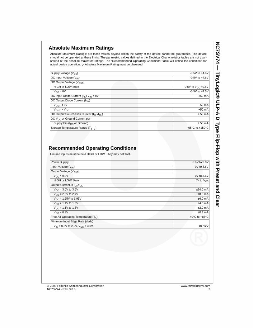
Absolute Maximum RatingsAbsolute Maximum Ratings: are those values beyond which the safety of the device cannot be guaranteed. The deviceshould not be operated at these limits. The parametric values defined in the Electrical Characteristics tables are not guar-anteed at the absolute maximum ratings. The “Recommended Operating Conditions” table will define the conditions foractual device operation. IO Absolute Maximum Rating must be observed.
Recommended Operating ConditionsUnused inputs must be held HIGH or LOW. They may not float.
Supply Voltage (VCC) -0.5V to +4.6V
DC Input Voltage (VIN) -0.5V to +4.6V
DC Output Voltage (VOUT)
HIGH or LOW State -0.5V to VCC +0.5V
VCC = 0V -0.5V to +4.6V
DC Input Diode Current (IIK) VIN < 0V ±50 mA
DC Output Diode Current (IOK)
VOUT < 0V -50 mA
VOUT > VCC +50 mA
DC Output Source/Sink Current (IOH/IOL) ± 50 mA
DC VCC or Ground Current per
Supply Pin (ICC or Ground) ± 50 mA
Storage Temperature Range (TSTG) -65°C to +150°C
Power Supply 0.9V to 3.6V
Input Voltage (VIN) 0V to 3.6V
Output Voltage (VOUT)
VCC = 0.0V 0V to 3.6V
HIGH or LOW State 0V to VCC
Output Current in IOH/IOL
VCC = 3.0V to 3.6V ±24.0 mA
VCC = 2.3V to 2.7V ±18.0 mA
VCC = 1.65V to 1.95V ±6.0 mA
VCC = 1.4V to 1.6V ±4.0 mA
VCC = 1.1V to 1.3V ±2.0 mA
VCC = 0.9V ±0.1 mA
Free Air Operating Temperature (TA) -40°C to +85°C
Minimum Input Edge Rate (dt/dv)
VIN = 0.8V to 2.0V, VCC = 3.0V 10 ns/V
NC
7SV
74 — T
inyL
og
ic® U
LP
-A D
Typ
e Flip
-Flo
p w
ith P
reset and
Clear
© 2003 Fairchild Semiconductor Corporation www.fairchildsemi.comNC7SV74 • Rev. 3.0.0 4
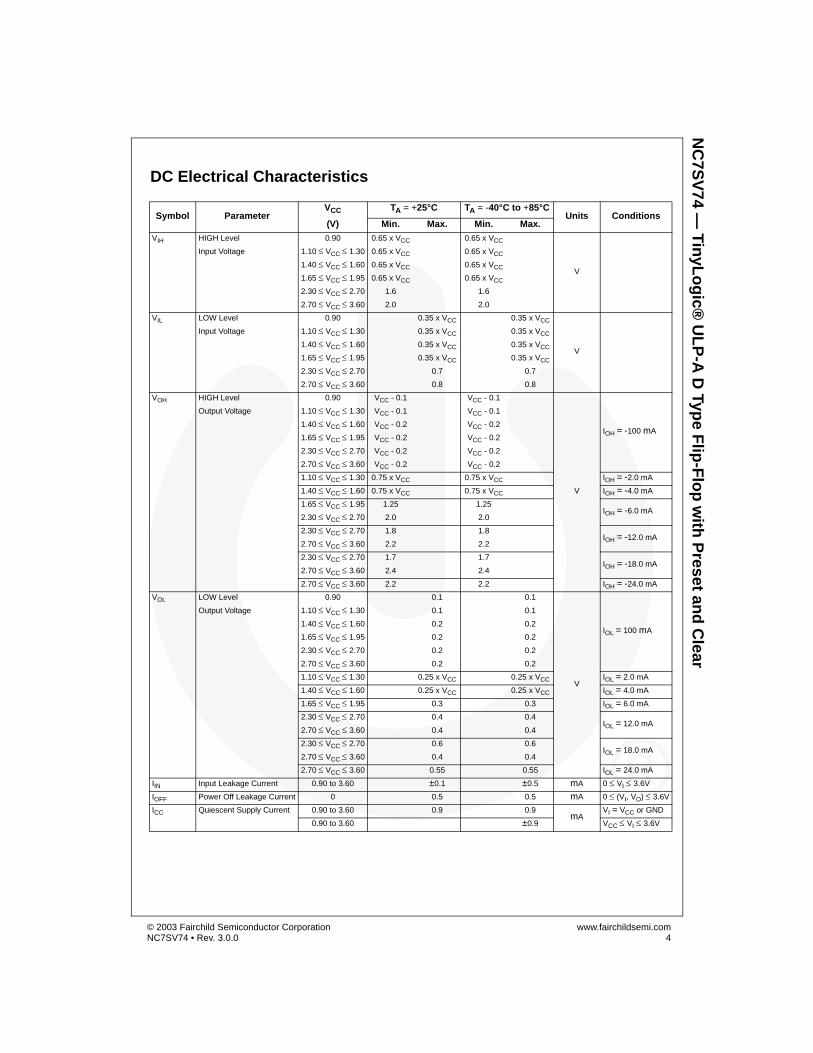
DC Electrical Characteristics
Symbol ParameterVCC TA = +25°C TA = -40°C to +85°C
Units Conditions(V) Min. Max. Min. Max.
VIH HIGH Level 0.90 0.65 x VCC 0.65 x VCC
V
Input Voltage 1.10 VCC 1.30 0.65 x VCC 0.65 x VCC
1.40 VCC 1.60 0.65 x VCC 0.65 x VCC
1.65 VCC 1.95 0.65 x VCC 0.65 x VCC
2.30 VCC 2.70 1.6 1.6
2.70 VCC 3.60 2.0 2.0
VIL LOW Level 0.90 0.35 x VCC 0.35 x VCC
V
Input Voltage 1.10 VCC 1.30 0.35 x VCC 0.35 x VCC
1.40 VCC 1.60 0.35 x VCC 0.35 x VCC
1.65 VCC 1.95 0.35 x VCC 0.35 x VCC
2.30 VCC 2.70 0.7 0.7
2.70 VCC 3.60 0.8 0.8
VOH HIGH Level 0.90 VCC - 0.1 VCC - 0.1
V
IOH = -100 mA
Output Voltage 1.10 VCC 1.30 VCC - 0.1 VCC - 0.1
1.40 VCC 1.60 VCC - 0.2 VCC - 0.2
1.65 VCC 1.95 VCC - 0.2 VCC - 0.2
2.30 VCC 2.70 VCC - 0.2 VCC - 0.2
2.70 VCC 3.60 VCC - 0.2 VCC - 0.2
1.10 VCC 1.30 0.75 x VCC 0.75 x VCC IOH = -2.0 mA
1.40 VCC 1.60 0.75 x VCC 0.75 x VCC IOH = -4.0 mA
1.65 VCC 1.95 1.25 1.25IOH = -6.0 mA
2.30 VCC 2.70 2.0 2.0
2.30 VCC 2.70 1.8 1.8IOH = -12.0 mA
2.70 VCC 3.60 2.2 2.2
2.30 VCC 2.70 1.7 1.7IOH = -18.0 mA
2.70 VCC 3.60 2.4 2.4
2.70 VCC 3.60 2.2 2.2 IOH = -24.0 mA
VOL LOW Level 0.90 0.1 0.1
V
IOL = 100 mA
Output Voltage 1.10 VCC 1.30 0.1 0.1
1.40 VCC 1.60 0.2 0.2
1.65 VCC 1.95 0.2 0.2
2.30 VCC 2.70 0.2 0.2
2.70 VCC 3.60 0.2 0.2
1.10 VCC 1.30 0.25 x VCC 0.25 x VCC IOL = 2.0 mA
1.40 VCC 1.60 0.25 x VCC 0.25 x VCC IOL = 4.0 mA
1.65 VCC 1.95 0.3 0.3 IOL = 6.0 mA
2.30 VCC 2.70 0.4 0.4IOL = 12.0 mA
2.70 VCC 3.60 0.4 0.4
2.30 VCC 2.70 0.6 0.6IOL = 18.0 mA
2.70 VCC 3.60 0.4 0.4
2.70 VCC 3.60 0.55 0.55 IOL = 24.0 mA
IIN Input Leakage Current 0.90 to 3.60 ±0.1 ±0.5 mA 0 VI 3.6V
IOFF Power Off Leakage Current 0 0.5 0.5 mA 0 (VI, VO) 3.6V
ICC Quiescent Supply Current 0.90 to 3.60 0.9 0.9mA
VI = VCC or GND
0.90 to 3.60 ±0.9 VCC VI 3.6V
NC
7SV
74 — T
inyL
og
ic® U
LP
-A D
Type
Flip
-Flo
p w
ith P
reset and
Clear
© 2003 Fairchild Semiconductor Corporation www.fairchildsemi.comNC7SV74 • Rev. 3.0.0 5
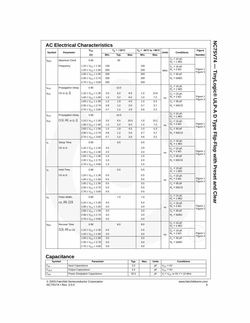
AC Electrical Characteristics
Capacitance
Symbol ParameterVCC TA = +25°C TA = -40°C to +85°C
Units ConditionsFigure
(V) Min. Typ. Max. Min. Max. Number
fMAX Maximum Clock 0.90 50
MHz
CL = 15 pF, RL = 1 M
Figure 1Figure 5
Frequency 1.10 VCC 1.30 150 150 CL = 15 pF, RL = 2 k1.40 VCC 1.60 200 200
1.65 VCC 1.95 200 200 CL = 30 pF
2.30 VCC 2.70 200 200 RL = 5002.70 VCC 3.60 200 200
tPLH Propagation Delay 0.90 13.0
ns
CL = 15 pF, RL = 1 M
Figure 1Figure 3
tPHL CK to Q, Q 1.10 VCC 1.30 3.0 6.0 9.9 1.0 14.6 CL = 15 pF, RL = 2 k1.40 VCC 1.60 1.0 3.2 6.0 1.0 7.2
1.65 VCC 1.95 1.0 1.9 4.5 1.0 5.3 CL = 30 pF
2.30 VCC 2.70 0.8 1.2 3.0 0.7 3.7 RL = 500 2.70 VCC 3.60 0.7 1.0 2.8 0.6 3.2
tPLH Propagation Delay 0.90 14.0
ns
CL = 15 pF, RL = 1 M
Figure 1Figure 3
tPHL CLR, PR, to Q, Q 1.10 VCC 1.30 3.0 6.5 10.5 1.0 15.1 CL = 15 pF, RL = 2 k1.40 VCC 1.60 1.0 3.2 6.0 1.0 7.2
1.65 VCC 1.95 1.0 1.9 4.5 1.0 5.3 CL = 30 pF
2.30 VCC 2.70 0.8 1.2 3.0 0.7 3.7 RL = 500 2.70 VCC 3.60 0.7 1.0 2.8 0.6 3.2
tS Setup Time, 0.90 6.5 6.5
ns
CL = 15 pF, RL = 1 M
Figure 1Figure 4
CK to D 1.10 VCC 1.30 3.5 3.5 CL = 15 pF, RL = 2 k1.40 VCC 1.60 2.0 2.0
1.65 VCC 1.95 1.5 1.5 CL = 30 pF
2.30 VCC 2.70 2.0 2.0 RL = 500 2.70 VCC 3.60 1.5 1.5
tH Hold Time, 0.90 0.5 0.5
ns
CL = 15 pF, RL = 1 M
Figure 1Figure 4
CK to D 1.10 VCC 1.30 0.5 0.5 CL = 15 pF, RL = 2 k1.40 VCC 1.60 0.5 0.5
1.65 VCC 1.95 0.5 0.5 CL = 30 pF
2.30 VCC 2.70 0.5 0.5 RL = 500 2.70 VCC 3.60 0.5 0.5
tW Pulse Width, 0.90 7.0 7.0
ns
CL = 15 pF, RL = 1 M
Figure 1Figure 5
CK, PR, CLR 1.10 VCC 1.30 4.0 4.0 CL = 15 pF, RL = 2 k1.40 VCC 1.60 3.0 3.0
1.65 VCC 1.95 3.0 3.0 CL = 30 pF
2.30 VCC 2.70 3.0 3.0 RL = 5002.70 VCC 3.60 3.0 3.0
tREC Recover Time 0.90 8.0 8.0
ns
CL = 15 pF, RL = 1 M
Figure 1Figure 4
CLR, PR to CK 1.10 VCC 1.30 4.5 4.5 CL = 15 pF, RL = 2 k1.40 VCC 1.60 3.0 3.0
1.65 VCC 1.95 3.0 3.0 CL = 30 pF
2.30 VCC 2.70 3.0 3.0 RL = 5002.70 VCC 3.60 3.0 3.0
Symbol Parameter Typ. Max. Units Conditions
CIN Input Capacitance 2.0 pF VCC = 0V
COUT Output Capacitance 4.5 pF VCC = 0V
CPD Power Dissipation Capacitance 20.0 pF VI = VCC or 0V, f = 10 MHz
NC
7SV
74 — T
inyL
og
ic® U
LP
-A D
Type F
lip-F
lop
with
Preset an
d C
lear
© 2003 Fairchild Semiconductor Corporation www.fairchildsemi.comNC7SV74 • Rev. 3.0.0 6
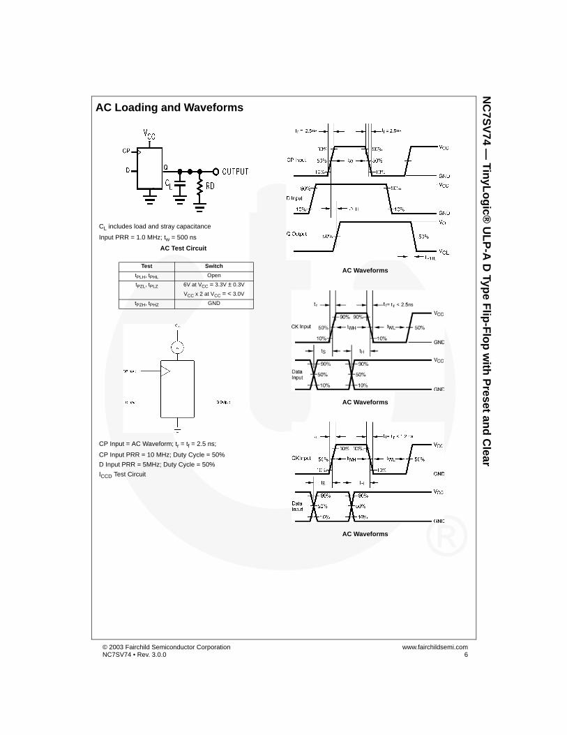
AC Loading and Waveforms
CL includes load and stray capacitance
Input PRR = 1.0 MHz; tw = 500 ns
AC Test Circuit
CP Input = AC Waveform; tr = tf = 2.5 ns;
CP Input PRR = 10 MHz; Duty Cycle = 50%
D Input PRR = 5MHz; Duty Cycle = 50%
ICCD Test Circuit
AC Waveforms
AC Waveforms
AC Waveforms
Test Switch
tPLH, tPHL Open
tPZL, tPLZ 6V at VCC = 3.3V ± 0.3V
VCC x 2 at VCC = < 3.0V
tPZH, tPHZ GND
NC
7SV
74 — T
inyL
og
ic® U
LP
-A D
Type
Flip
-Flo
p w
ith P
reset and
Clear
© 2003 Fairchild Semiconductor Corporation www.fairchildsemi.comNC7SV74 • Rev. 3.0.0 7
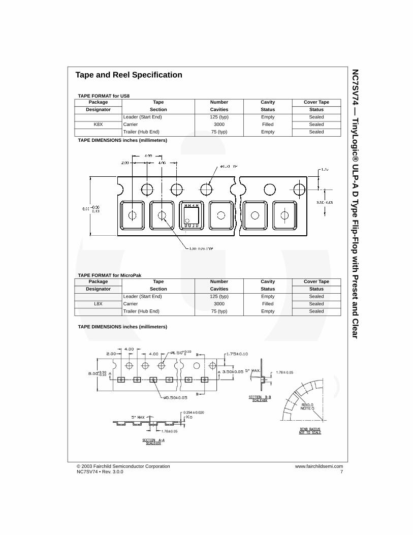
Tape and Reel Specification
TAPE FORMAT for US8
TAPE DIMENSIONS inches (millimeters)
TAPE FORMAT for MicroPak
TAPE DIMENSIONS inches (millimeters)
Package Tape Number Cavity Cover Tape
Designator Section Cavities Status Status
Leader (Start End) 125 (typ) Empty Sealed
K8X Carrier 3000 Filled Sealed
Trailer (Hub End) 75 (typ) Empty Sealed
Package Tape Number Cavity Cover Tape
Designator Section Cavities Status Status
Leader (Start End) 125 (typ) Empty Sealed
L8X Carrier 3000 Filled Sealed
Trailer (Hub End) 75 (typ) Empty Sealed
NC
7SV
74 — T
inyL
og
ic® U
LP
-A D
Type F
lip-F
lop
with
Preset an
d C
lear
© 2003 Fairchild Semiconductor Corporation www.fairchildsemi.comNC7SV74 • Rev. 3.0.0 8
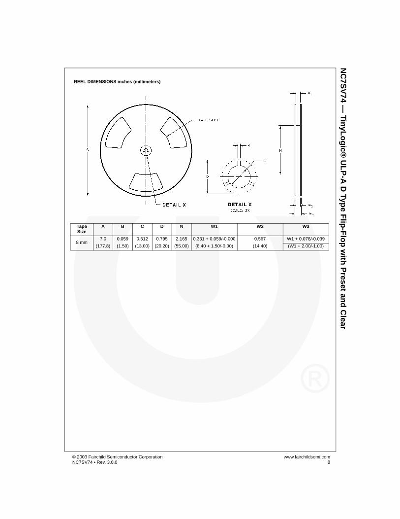
REEL DIMENSIONS inches (millimeters)
Tape Size
A B C D N W1 W2 W3
8 mm7.0 0.059 0.512 0.795 2.165 0.331 + 0.059/-0.000 0.567 W1 + 0.078/-0.039
(177.8) (1.50) (13.00) (20.20) (55.00) (8.40 + 1.50/-0.00) (14.40) (W1 + 2.00/-1.00)
NC
7SV
74 — T
inyL
og
ic® U
LP
-A D
Type
Flip
-Flo
p w
ith P
reset and
Clear
© 2003 Fairchild Semiconductor Corporation www.fairchildsemi.comNC7SV74 • Rev. 3.0.0 9
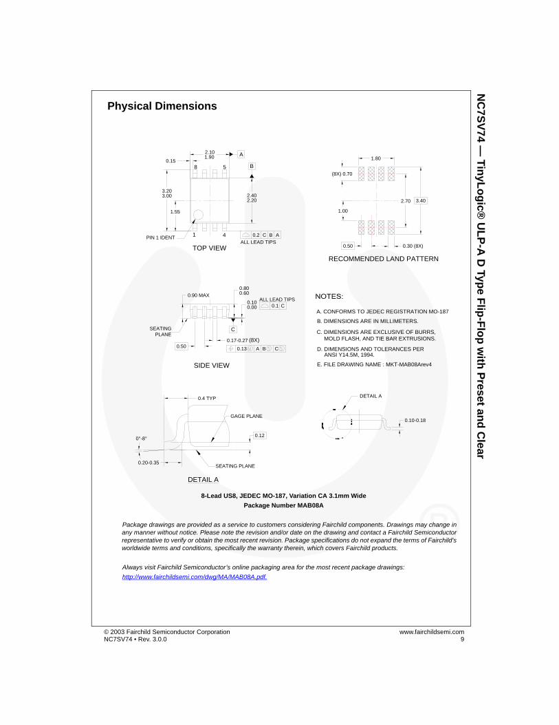
Physical Dimensions
8-Lead US8, JEDEC MO-187, Variation CA 3.1mm Wide
Package Number MAB08A
Package drawings are provided as a service to customers considering Fairchild components. Drawings may change inany manner without notice. Please note the revision and/or date on the drawing and contact a Fairchild Semiconductorrepresentative to verify or obtain the most recent revision. Package specifications do not expand the terms of Fairchild’sworldwide terms and conditions, specifically the warranty therein, which covers Fairchild products.
Always visit Fairchild Semiconductor’s online packaging area for the most recent package drawings:
http://www.fairchildsemi.com/dwg/MA/MAB08A.pdf.
SIDE VIEW
TOP VIEW
RECOMMENDED LAND PATTERN
A
B
0.50
SEATING PLANE
0.10-0.18
0.13 A B C0.50
DETAIL A
0.4 TYP
ALL LEAD TIPS
0.2 C B A PIN 1 IDENT
ALL LEAD TIPS0.1 C
8
1 4
5(8X) 0.70
2.70 3.40
1.00
DETAIL A
1.80
GAGE PLANE
0.12
C. DIMENSIONS ARE EXCLUSIVE OF BURRS,
D. DIMENSIONS AND TOLERANCES PER
MOLD FLASH, AND TIE BAR EXTRUSIONS.
B. DIMENSIONS ARE IN MILLIMETERS.
A. CONFORMS TO JEDEC REGISTRATION MO-187
ANSI Y14.5M, 1994.
2.101.90
2.402.20
0.15
3.203.00
1.55
0.90 MAX
0.100.00
0.800.60
0.17-0.27 (8X)
0.30 (8X)
0.20-0.35
0°-8°
CSEATINGPLANE
E. FILE DRAWING NAME : MKT-MAB08Arev4
NC
7SV
74 — T
inyL
og
ic® U
LP
-A D
Type F
lip-F
lop
with
Preset an
d C
lear
© 2003 Fairchild Semiconductor Corporation www.fairchildsemi.comNC7SV74 • Rev. 3.0.0 10
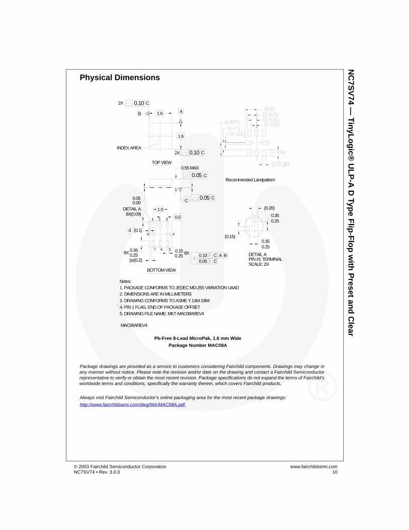
Physical Dimensions
Pb-Free 8-Lead MicroPak, 1.6 mm Wide
Package Number MAC08A
Package drawings are provided as a service to customers considering Fairchild components. Drawings may change inany manner without notice. Please note the revision and/or date on the drawing and contact a Fairchild Semiconductorrepresentative to verify or obtain the most recent revision. Package specifications do not expand the terms of Fairchild’sworldwide terms and conditions, specifically the warranty therein, which covers Fairchild products.
Always visit Fairchild Semiconductor’s online packaging area for the most recent package drawings:
http://www.fairchildsemi.com/dwg/MA/MAC08A.pdf.
(0.09)
(0.1)
(0.2)
1.6
2X
0.050.00
1.6
2X
C 0.05 C
4
3. DRAWING CONFORMS TO ASME Y.14M-1994
2. DIMENSIONS ARE IN MILLIMETERS1. PACKAGE CONFORMS TO JEDEC MO-255 VARIATION UAAD
BOTTOM VIEW
4. PIN 1 FLAG, END OF PACKAGE OFFSET
MAC08AREV4
1 2 3
567
8
Notes:
8X 0.250.35
3X
8X1.0
4
0.5
8X0.250.15
0.10 C A B0.05 C
0.10 C
TOP VIEW
INDEX AREA
B
Recommended Landpattern
A
0.10 C
0.55 MAX
0.05 C
DETAIL A
0.350.25
(0.15)
(0.20)
0.350.25
DETAIL APIN #1 TERMINALSCALE: 2X
5. DRAWING FILE NAME: MKT-MAC08AREV4
NC
7SV
74 — T
inyL
og
ic® U
LP
-A D
Type
Flip
-Flo
p w
ith P
reset and
Clear
© 2003 Fairchild Semiconductor Corporation www.fairchildsemi.comNC7SV74 • Rev. 3.0.0 11
NC
7SV
74 — T
inyL
og
ic® U
LP
-A D
Type F
lip-F
lop
with
Preset an
d C
lear
www.onsemi.com1
ON Semiconductor and are trademarks of Semiconductor Components Industries, LLC dba ON Semiconductor or its subsidiaries in the United States and/or other countries.ON Semiconductor owns the rights to a number of patents, trademarks, copyrights, trade secrets, and other intellectual property. A listing of ON Semiconductor’s product/patentcoverage may be accessed at www.onsemi.com/site/pdf/Patent−Marking.pdf. ON Semiconductor reserves the right to make changes without further notice to any products herein.ON Semiconductor makes no warranty, representation or guarantee regarding the suitability of its products for any particular purpose, nor does ON Semiconductor assume any liabilityarising out of the application or use of any product or circuit, and specifically disclaims any and all liability, including without limitation special, consequential or incidental damages.Buyer is responsible for its products and applications using ON Semiconductor products, including compliance with all laws, regulations and safety requirements or standards,regardless of any support or applications information provided by ON Semiconductor. “Typical” parameters which may be provided in ON Semiconductor data sheets and/orspecifications can and do vary in different applications and actual performance may vary over time. All operating parameters, including “Typicals” must be validated for each customerapplication by customer’s technical experts. ON Semiconductor does not convey any license under its patent rights nor the rights of others. ON Semiconductor products are notdesigned, intended, or authorized for use as a critical component in life support systems or any FDA Class 3 medical devices or medical devices with a same or similar classificationin a foreign jurisdiction or any devices intended for implantation in the human body. Should Buyer purchase or use ON Semiconductor products for any such unintended or unauthorizedapplication, Buyer shall indemnify and hold ON Semiconductor and its officers, employees, subsidiaries, affiliates, and distributors harmless against all claims, costs, damages, andexpenses, and reasonable attorney fees arising out of, directly or indirectly, any claim of personal injury or death associated with such unintended or unauthorized use, even if suchclaim alleges that ON Semiconductor was negligent regarding the design or manufacture of the part. ON Semiconductor is an Equal Opportunity/Affirmative Action Employer. Thisliterature is subject to all applicable copyright laws and is not for resale in any manner.
PUBLICATION ORDERING INFORMATIONN. American Technical Support: 800−282−9855 Toll FreeUSA/Canada
Europe, Middle East and Africa Technical Support:Phone: 421 33 790 2910
Japan Customer Focus CenterPhone: 81−3−5817−1050
www.onsemi.com
LITERATURE FULFILLMENT:Literature Distribution Center for ON Semiconductor19521 E. 32nd Pkwy, Aurora, Colorado 80011 USAPhone: 303−675−2175 or 800−344−3860 Toll Free USA/CanadaFax: 303−675−2176 or 800−344−3867 Toll Free USA/CanadaEmail: [email protected]
ON Semiconductor Website: www.onsemi.com
Order Literature: http://www.onsemi.com/orderlit
For additional information, please contact your localSales Representative
© Semiconductor Components Industries, LLC


![- É{Z f«Y Ä Âe Á É Y~´f ZÌ ] ½M ÉZÅ|»ZÌa Á Ê ¼m À¯ ª À»€¦ · Z] d ZÌ º¸ Á ʻ¼ d ZÌ cZ ·Z » ʳ|ÌÀeºÅ { à Z] { Zf m ½YÂÀ Z] Ê ÅÁ a s](https://img.pdfslide.us/doc/110x75/60a28b94f3379c0d115fd4d3/z-fy-e-yf-zoe-m-zzoea-m-z-d.jpg)

![ry[ ý^ l³]ÝmAWßVóÿ X ]Ýÿ...Ý T p,]Ý ^s b8 l8 7]Ý ?NET ]Ý [ u0]Ý 0D0_0a]Ý T lÉ gÏ \>]Ý X ]Ý N X SAN b@ {9vî u: OPR©ÿ N vî WB0ÎN m% ÿ N ê0ÎN ÿ N vî OPR©ÿ](https://img.pdfslide.us/doc/110x75/5f3727a7e88bbd492d3bfe25/ry-lmawv-x-t-p-s-b8-l8-7-net-u0-0d00a.jpg)

![Üæ æ ÝZÕ ´¯ ì °» ˆ ì ƒ ì ìó –ça ÆšƒˇÖ]Ý]‡ìäfjÓÚ ìó ...¯å„äwDZ)·Xµ%»óìóB gW Zì˙ ]! ”—w−LL¯gzZìq Z—~ Ž…yi'¤~‹yM„Ûäsßær](https://img.pdfslide.us/doc/110x75/5e4d463115484a3e3064a448/oe-z-aa-afj-.jpg)


![f 2 f ) } ¨ ¯ l µ - CASIO Official Website2 クイックメニュー $ e * 2 L 6 2 ; & f = 1 ¥ * 2 t ¡ ± ½ ¿ e X ] G $ 2 a ¿ e , ð * 2 ² p ý ¥ w ¯ p ý ý > 1 ý ý ý](https://img.pdfslide.us/doc/110x75/611a0bad23668c16ac329a59/f-2-f-l-casio-official-website-2-ffffff-e-2.jpg)


![Ý Ý Ý hÈÕÕÑÙ=ÇÒÒhÔËÚ z] 1 /s4 y, ke · Created Date: 20091111170056Z](https://img.pdfslide.us/doc/110x75/5f1d9de0bfbf1d360051f114/-hh-z-1-s4-y-ke-created-date-20091111170056z.jpg)