Embed Size (px)
Citation preview

S-5470 Series
www.ablicinc.com
ULTRA-LOW CURRENT CONSUMPTION NORMALLY-OFF FAINT SIGNAL DETECTION IC
© ABLIC Inc., 2012-2016 Rev.1.3_02
1
The S-5470 Series, developed by CMOS technology, is a normally-off faint signal detection IC with an ultra-low current consumption. This IC has a function to detect certain current level of 0.7 nA typ., which makes it possible to detect faint signals for a variety of electric generating devices or sensor devices. It also has a function to detect the difference of current level, and thus detects difference between strengths of two signals input at the same time. Due to its ultra-low current consumption and low-voltage operation, the S-5470 Series is suitable for battery-operated small mobile device applications.
Features
Ultra-low current consumption: IDD 0.1 nA typ. Faint current detection: IDET = 0.7 nA typ. Wide operation voltage range: VDD = 0.9 V to 5.5 V Detection of faint signal: Detects faint signals of approximately 0.7 nW (1.0 V, 0.7 nA typ.) Detection of signal strength difference: Detects difference between strengths of two signals input at the same time Lead-free (Sn 100%), halogen-free
Applications
Detects output signals of electric generating devices or sensor devices with high internal resistance Advanced sensing using two electric generating devices or sensor devices Miniaturization and low power consumption for various sensors of portable and wireless devices
Package
SOT-23-5

ULTRA-LOW CURRENT CONSUMPTION NORMALLY-OFF FAINT SIGNAL DETECTION IC S-5470 Series Rev.1.3_02
2
Block Diagrams 1. CMOS output product
OUT
*1
*1
VDD
VSS
INP
INM *1
*1
IDET
*1
Current comparator
Current amplifier
Logic selection
Current adder
*1. Parasitic diode Figure 1
2. Nch open-drain output product
OUT
*1
VDD
VSS
INP
INM *1
*1
IDET
*1
Current comparator
Current amplifier
Logic selection
Current adder
*1. Parasitic diode Figure 2

ULTRA-LOW CURRENT CONSUMPTION NORMALLY-OFF FAINT SIGNAL DETECTION ICRev.1.3_02 S-5470 Series
3
Product Name Structure
Users can select the output form and output logic for the S-5470 Series. Refer to "1. Product name" regarding the contents of the product name, "2. Package" regarding the package drawings, "3. Product name list" regarding details of the product name.
1. Product name
S-5470 x 21 I - M5T1 U
Environmental code U: Lead-free (Sn 100%), halogen-free Package abbreviation and IC packing specifications*1 M5T1: SOT-23-5, Tape Operation temperature I: Ta = 40C to 85C Detection mode 21: Current amplifier current amplification ratio 2 Output form and output logic A: CMOS output (Active "H") B: CMOS output (Active "L") C: Nch open-drain output (Active "H") D: Nch open-drain output (Active "L")
*1. Refer to the tape drawing.
2. Package
Table 1 Package Drawing Codes
Package Name Dimension Tape Reel
SOT-23-5 MP005-A-P-SD MP005-A-C-SD MP005-A-R-SD
3. Product name list
Table 2
Product Name Output Form Output Logic Detection Mode
S-5470A21I-M5T1U CMOS output Active "H" Current amplifier current amplification ratio 2
S-5470B21I-M5T1U CMOS output Active "L" Current amplifier current amplification ratio 2
S-5470C21I-M5T1U Nch open-drain output Active "H" Current amplifier current amplification ratio 2
S-5470D21I-M5T1U Nch open-drain output Active "L" Current amplifier current amplification ratio 2
Remark Please contact our sales office for products other than the above.

ULTRA-LOW CURRENT CONSUMPTION NORMALLY-OFF FAINT SIGNAL DETECTION IC S-5470 Series Rev.1.3_02
4
Pin Configuration
1. SOT-23-5
1 32
45
Top view
Table 3
Pin No. Symbol Description
1 VDD Power supply pin
2 VSS GND pin
3 INM Reference current input pin
4 INP Detection current input pin
5 OUT Output pin
Figure 3

ULTRA-LOW CURRENT CONSUMPTION NORMALLY-OFF FAINT SIGNAL DETECTION ICRev.1.3_02 S-5470 Series
5
Absolute Maximum Ratings
Table 4
(Ta = 25°C unless otherwise specified)
Item Symbol Absolute Maximum Rating Unit
Power supply voltage VDD VSS 0.3 to VSS 7.0 V
Input voltage VINP, VINM VSS 0.3 to VSS 7.0 V
Output voltage CMOS output product
VOUT VSS 0.3 to VDD 0.3 V
Nch open-drain output product VSS 0.3 to VSS 7.0 V
Output pin current ISOURCE 20 mA
ISINK 20 mA
Power dissipation PD 600*1 mW
Operation ambient temperature Topr 40 to 85 °C
Storage temperature Tstg 55 to 125 °C
*1. When mounted on board [Mounted board]
(1) Board size: 114.3 mm 76.2 mm t1.6 mm (2) Name: JEDEC STANDARD51-7
Caution The absolute maximum ratings are rated values exceeding which the product could suffer
physical damage. These values must therefore not be exceeded under any conditions.
0 50 100 1500
Pow
er D
issi
patio
n (P
D)
[mW
]
Ambient Temperature (Ta) [C]
200
100
300
500
700
400
600
Figure 4 Power Dissipation of Package (When Mounted on Board)

ULTRA-LOW CURRENT CONSUMPTION NORMALLY-OFF FAINT SIGNAL DETECTION IC S-5470 Series Rev.1.3_02
6
Electrical Characteristics
Table 5
(Ta = 25°C, VDD = 3.0 V unless otherwise specified)
Item Symbol Condition Min. Typ. Max. Unit Test
Circuit
Power supply voltage VDD Ta = 40°C to 85°C 0.9 5.5 V
Current consumption IDD VINP = VSS, VINM = VSS 0.01 10 nA 1
VINP = 1.0 V, VINM = VSS 0.02 10 nA 1
Detection current IDET 0.52 0.7 0.88 nA 2
Release current IREL IDET 0.7
IDET 0.8
IDET 0.9
nA 2
Detection current temperature coefficient
Itc Ta = 40°C to 85°C 0.5 %°C
Input current IINP VINP = 1.0 V 20 A 3
IINM VINM = 1.0 V 10 A 3
Current amplifier current amplification ratio 2
GINM 1.8 2.0 2.2 Times 4
Source current ISOURCE CMOS output productVOUT = VDD 0.3 V
VDD = 0.9 V 0.01 0.4 mA 5
VDD = 3.0 V 3.5 4.8 mA 5
Sink current ISINK VOUT = 0.3 V VDD = 0.9 V 0.5 1.7 mA 6
VDD = 3.0 V 7.0 9.2 mA 6
Output response time tOD 15 ms

ULTRA-LOW CURRENT CONSUMPTION NORMALLY-OFF FAINT SIGNAL DETECTION ICRev.1.3_02 S-5470 Series
7
Test Circuits
A VDD
OUT
VSS
S-5470 Series
INP
INM
R*1
100 k
VDD
OUT
VSS
S-5470 Series
INP
INM
R*1
100 k
V
*1. Resistor (R) is unnecessary for the CMOS output product. *1. Resistor (R) is unnecessary for the CMOS output product.
Figure 5 Test Circuit 1 Figure 6 Test Circuit 2
VDD
OUT
VSS
S-5470 Series
INP
INM
A
A Open
VDD
OUT
VSS
S-5470 Series
INP
INM
R*1
100 k
V
*1. Resistor (R) is unnecessary for the CMOS output product.
Figure 7 Test Circuit 3 Figure 8 Test Circuit 4
VDD
OUT
VSS
S-5470 Series
INP
INM
A
VDD
OUT
VSS
S-5470 Series
INP
INM A
Figure 9 Test Circuit 5 Figure 10 Test Circuit 6

ULTRA-LOW CURRENT CONSUMPTION NORMALLY-OFF FAINT SIGNAL DETECTION IC S-5470 Series Rev.1.3_02
8
Standard Circuits
1. Certain current level detector
VDD
OUT
VSS
S-5470 Series
INP
INM
VOUT
0.1 F IINP R*1
100 k
*1. Resistor (R) is unnecessary for the CMOS output product.
Figure 11
2. Current level difference detector
VDD
OUT
VSS
S-5470 Series
INP
INM
IINP
IINM
VOUT
0.1 FR*1
100 k
*1. Resistor (R) is unnecessary for the CMOS output product.
Figure 12
Caution The above connection diagram and constant will not guarantee successful operation. Perform thorough evaluation using the actual application to set the constant.

ULTRA-LOW CURRENT CONSUMPTION NORMALLY-OFF FAINT SIGNAL DETECTION ICRev.1.3_02 S-5470 Series
9
Operation
The S-5470 Series detects either certain current level or the difference of current level. The operation of the S-5470 Series is described below, using CMOS output and active "H" products as examples.
1. Basic operation when detecting certain current level (INM pin = VSS)
The S-5470 Series operates as follows when the INM pin is connected to VSS pin.
(1) If IINP is lower than IDET, an "L" level signal is output from the OUT pin. (2) If IINP increases and becomes equal to or higher than IDET, an "H" level signal is output from the OUT pin (point
A in Figure 14). Even if IINP decreases and falls below IDET, as long as IINP is higher than IREL, an "H" level signal is output from the OUT pin.
(3) If IINP then decreases further and becomes equal to or lower than IREL, an "L" level signal is output from the OUT pin (point B in Figure 14).
Remark IINP: Current input to the INP pin IDET: Detection current (refer to "4. 1 Detection current (IDET)") IREL: Release current (refer to "4. 2 Release current (IREL)")
Caution 1. There are internal diodes at the INP pin and the INM pin. Therefore, in order to input a current
to the INP pin and the INM pin, an input voltage of at least the forward voltage of these diodes is required.
2. Feed-through current (IPEAK = 100 nA) flows around the time when the OUT pin voltage switches, as shown in Figure 14. Therefore, if the input current is fixed around this time, the current consumption will increase.
OUT
*1
*1
INP
INM
*1
*1
IDET
IINP
VDD
VSS
*1
Current comparator
Current amplifier
Current adder
IINP
*1. Parasitic diode
Figure 13 Diagram of the Operation when Detecting Certain Current Level
IINP
H
L
Current consumption (IDD)
IPEAK = 100 nA
OUT pin output voltage (VOUT)
IDET
IREL
Hysteresis widthBA
(3) (1) (2)
Figure 14 Operation when Detecting Certain Current Level

ULTRA-LOW CURRENT CONSUMPTION NORMALLY-OFF FAINT SIGNAL DETECTION IC S-5470 Series Rev.1.3_02
10
2. Basic operation when detecting the difference of current level (Current amplifier current amplification ratio GINM)
The S-5470 Series operates as follows when current (IINM) is applied to the INM pin.
(1) If IINP is lower than IDET GINM IINM, an "L" level signal is output from the OUT pin. (2) If IINP increases and becomes equal to or higher than IDET GINM IINM, an "H" level signal is output from the
OUT pin (point A in Figure 16). Even if IINP decreases and falls below IDET GINM IINM, as long as IINP is higher than IREL GINM IINM, an "H" level signal is output from the OUT pin.
(3) If IINP then decreases further and becomes equal to or lower than IREL GINM IINM, an "L" level signal is output from the OUT pin (point B in Figure 16).
Remark IINP: Current input to the INP pin IINM: Current input to the INM pin IDET: Detection current (refer to "4. 1 Detection current (IDET)") IREL: Release current (refer to "4. 2 Release current (IREL)")
Caution 1. There are internal diodes at the INP pin and the INM pin. Therefore, in order to input a current
to the INP pin and the INM pin, an input voltage of at least the forward voltage of these diodes is required.
2. Feed-through current (IPEAK = 100 nA) flows around the time when the OUT pin voltage switches, as shown in Figure 16. Therefore, if the input current is fixed around this time, the current consumption will increase.
OUT
*1
*1
INP
INM*1
*1
IDET
IINP
VDD
VSS
*1
IINM Current comparator
Current amplifier
Current adder
IINP
IINM
*1. Parasitic diode Figure 15 Diagram of the Operation when Detecting the Difference of Current Level
IINP GINM IINM
H
L
Current consumption (IDD)
IPEAK = 100 nA
OUT pin output voltage (VOUT)
IDET
IREL
Hysteresis widthBA
(3) (1) (2)
Figure 16 Operation when Detecting the Difference of Current Level

ULTRA-LOW CURRENT CONSUMPTION NORMALLY-OFF FAINT SIGNAL DETECTION ICRev.1.3_02 S-5470 Series
11
3. Temperature characteristics of detection current
The shaded area in Figure 17 shows the temperature characteristics of the detection voltage in the operation temperature range.
40 25
0.5%/°C
IDET [nA]
85 Ta [°C]
0.5%/°C
IDET25*1
*1. IDET25: Detection current value at Ta = 25°C
Figure 17 Temperature Characteristics of Detection Current

ULTRA-LOW CURRENT CONSUMPTION NORMALLY-OFF FAINT SIGNAL DETECTION IC S-5470 Series Rev.1.3_02
12
4. Explanation of terms 4. 1 Detection current (IDET)
The detection current (IDET) is the current at which the output switches to "H". The detection current varies slightly even among products with the same specification. The variation in detection current from the minimum detection current (IDET min.) to the maximum detection current (IDET max.) is called the detection current range (refer to Figure 18).
Detection current
Detection
current range
IINP
IDET max.
IDET min.
VOUT
H
L
Figure 18 Detection Current
4. 2 Release current (IREL)
The release current (IREL) is the current at which the output switches to "L". The release current varies slightly even among products with the same specification. The variation in release current from the minimum release current (IREL min.) to the maximum release current (IREL max.) is called the release current range (refer to Figure 19). The range is calculated from the actual detection current (IDET) of a product and is in the range of IDET 0.7 IREL IDET 0.9.
Release current
Release
current range
IINP
IREL max.
IREL min.
VOUT
H
L
Figure 19 Release Current
4. 3 Hysteresis width
The hysteresis width is the current difference between the detection current and the release current (current at point B current at point A in "Figure 14 Operation when Detecting Certain Current Level" and "Figure 16 Operation when Detecting the Difference of Current Level"). The hysteresis width between the detection current and the release current prevents malfunction caused by noise in the input current.

ULTRA-LOW CURRENT CONSUMPTION NORMALLY-OFF FAINT SIGNAL DETECTION ICRev.1.3_02 S-5470 Series
13
Application Circuits
1. Certain photocurrent level detector
If PD or LED exceeds a certain value, the output signal inverts.
VDD
OUT
VSS
S-5470 Series
INP
INM
VOUT
0.1 F
D1
Figure 20 Example Certain Photocurrent Level Detector (CMOS Output Product)
VDD
OUT
VSS
S-5470 Series
INP
INM
VOUT
0.1 F R100 k
D1
Figure 21 Example Certain Photocurrent Level Detector (Nch Open-drain Output Product)
Caution The above connection diagram and constant will not guarantee successful operation. Perform thorough evaluation using the actual application to set the constant.

ULTRA-LOW CURRENT CONSUMPTION NORMALLY-OFF FAINT SIGNAL DETECTION IC S-5470 Series Rev.1.3_02
14
2. Photocurrent level difference detector
If the difference in the photocurrent generated by the two PDs or the two LEDs exceeds a certain value, the output signal inverts.
VDD
OUT
VSS
S-5470 Series
INP
INM
VOUT
0.1 F
D1 D2
Figure 22 Example Photocurrent Level Difference Detector (CMOS Output Product)
VDD
OUT
VSS
S-5470 Series
INP
INM
0.1 F
VOUT
R100 k
D1 D2
Figure 23 Example Photocurrent Level Difference Detector (Nch Open-drain Output Product)
Caution The above connection diagram and constant will not guarantee successful operation. Perform
thorough evaluation using the actual application to set the constant.

ULTRA-LOW CURRENT CONSUMPTION NORMALLY-OFF FAINT SIGNAL DETECTION ICRev.1.3_02 S-5470 Series
15
3. Selection of PD or LED
Use PD or LED whose generation voltage is 1.0 V or more under usable light quantity. Moreover, as for the test circuit shown in Figure 24, select PD or LED that satisfies the conditions below with detection or measurement of the quantity of light incidence in usage environment. Certain photocurrent level detector
IDET I Photocurrent level difference detector 1 nA I 20 A
Light incidence
1 V
I
A
D1, D2
Figure 24 Caution 1. Select PD or LED after thorough evaluation with actual application. ABLIC Inc. shall not take
responsibility for operation and characteristics of PD or LED. 2. As for the circuit of detecting photocurrent difference, shown in Figure 22 and Figure 23, use
the two PDs or the two LEDs that have the same characteristics in generation voltage and in generation current, respectively.

ULTRA-LOW CURRENT CONSUMPTION NORMALLY-OFF FAINT SIGNAL DETECTION IC S-5470 Series Rev.1.3_02
16
Precautions
Use the S-5470 Series with the output current of 20 mA or less. The S-5470 Series may malfunction if the power supply voltage changes suddenly.
As for the detecting circuit of the photocurrent difference (Refer to "Figure 22, Figure 23 Example Photocurrent Level Difference Detector"), use the S-5470 Series when input current of INP pin is 20 A or less and input current of INM pin is 10 A or less. In case of input current excess, note that the S-5470 Series might malfunction.
The output in the S-5470 Series is unstable in lower voltage than the minimum operation voltage. At the time of
power-on, use the S-5470 Series after output stabilization. Set a capacitor of 0.1 F or more between the VDD pin and VSS pin for stabilization. Since INP pin and INM pin is easy to be affected by disturbance noise, perform countermeasures such as
mounting external parts to ICs as close as possible. If power impedance is high, the S-5470 Series may malfunction due to voltage drop caused by feed-through current. Set wire patterns carefully for lower power impedance. Do not apply an electrostatic discharge to this IC that exceeds the performance ratings of the built-in electrostatic
protection circuit. ABLIC Inc. claims no responsibility for any disputes arising out of or in connection with any infringement by
products including this IC of patents owned by a third party.

ULTRA-LOW CURRENT CONSUMPTION NORMALLY-OFF FAINT SIGNAL DETECTION ICRev.1.3_02 S-5470 Series
17
Characteristics (Typical Data)
1. Detection current vs. Temperature 2. Detection current vs. Power supply voltage
VDD = 3.0 V Ta = 25C
IDE
T [n
A]
0.2
0.4
0.6
0.8
1.0
−40 0 25 50 75 85−25Ta [°C]
IDE
T [n
A]
0
0.4
0.2
0.6
0.8
1.0
0 2 3 4 5 61VDD [V]
3. Release current vs. Temperature 4. Release current vs. Power supply voltage
VDD = 3.0 V Ta = 25C
IRE
L [nA
]
0.2
0.4
0.6
0.8
1.0
−40 0 25 50 75 85−25Ta [°C]
IRE
L [nA
]
0
0.4
0.2
0.6
0.8
1.0
0 2 3 4 5 61VDD [V]
5. Current consumption vs. Temperature
VDD = 3.0 V
IDD [n
A]
0
1.0
2.0
3.0
−40 0 25 50 75 85−25Ta [°C]
VINP = 1 V
VINP = 0 V

ULTRA-LOW CURRENT CONSUMPTION NORMALLY-OFF FAINT SIGNAL DETECTION IC S-5470 Series Rev.1.3_02
18
6. Current consumption vs. Power supply
S-5470A21I Ta = 25C S-5470B21I Ta = 25C
IDD [n
A]
0
0.050.04
0.020.03
0.01
0.06
0 2 3 4 5 61VDD [V]
VINP = 0 V
VINP = 1 V
VDD [V]0 6
0.06
0
IDD [n
A]
54321
0.050.040.030.020.01
VINP = 1 V
VINP = 0 V
S-5470C21I Ta = 25C S-5470D21I Ta = 25C
VDD [V]0 6
0.06
0
IDD [n
A]
54321
0.050.040.030.020.01
VINP = 0 V
VINP = 1 V
VDD [V]0 6
0.06
0
IDD [n
A]
54321
0.050.040.030.020.01
VINP = 1 V
VINP = 0 V
7. Current amplifier current amplication ratio vs. Temperature
VDD = 3.0 V
GIN
M [t
imes
]
1.6
1.8
2.0
2.2
2.4
−40 0 25 50 75 85−25Ta [°C]
ULTRA-LOW CURRENT CONSUMPTION NORMALLY-OFF FAINT SIGNAL DETECTION ICRev.1.3_02 S-5470 Series
19
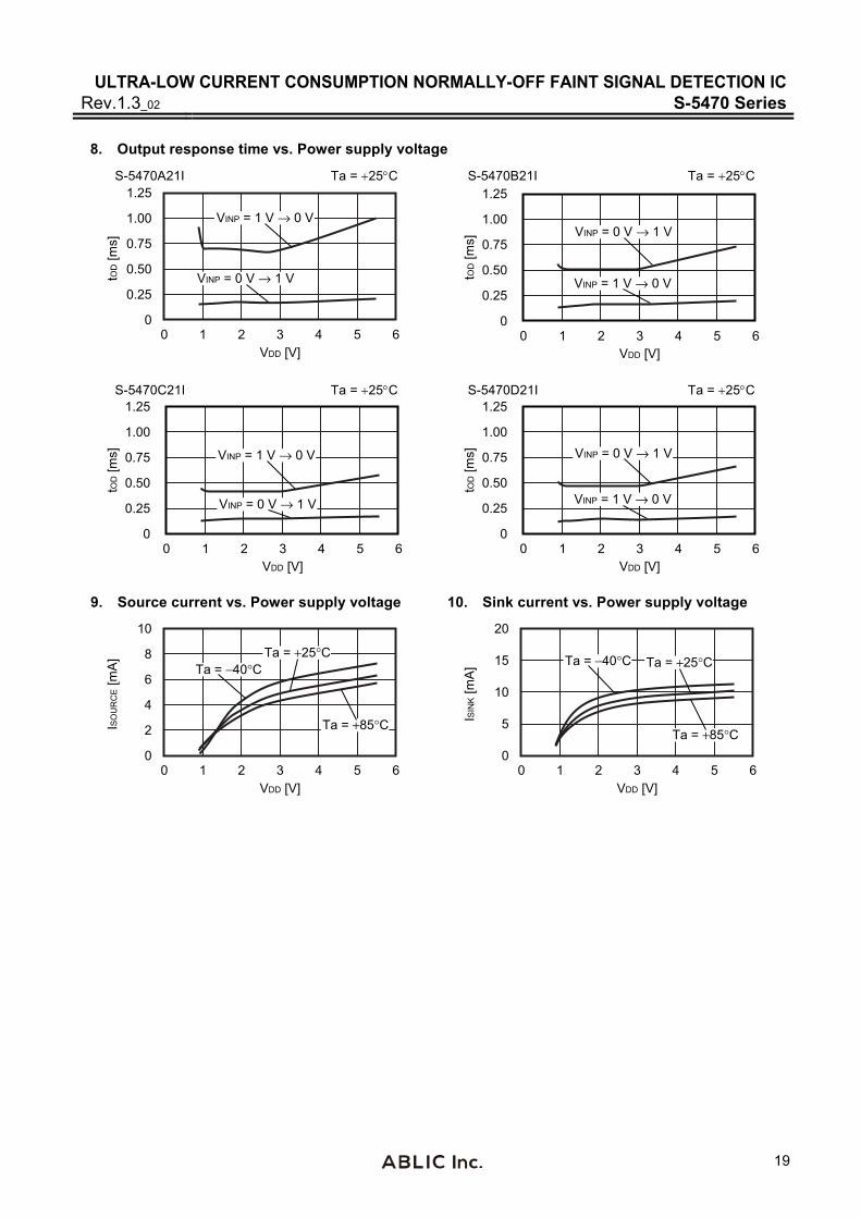
8. Output response time vs. Power supply voltage
S-5470A21I Ta = 25C S-5470B21I Ta = 25C
tOD [m
s]
0
0.75
0.50
0.25
1.00
1.25
0 2 3 4 5 61VDD [V]
VINP = 0 V → 1 V
VINP = 1 V → 0 V
VDD [V]0 6
1.25
0
tOD [m
s]
54321
1.00
0.75
0.50
0.25VINP = 1 V → 0 V
VINP = 0 V → 1 V
S-5470C21I Ta = 25C S-5470D21I Ta = 25C
VDD [V]0 6
1.25
0
tOD [m
s]
54321
1.00
0.75
0.50
0.25 VINP = 0 V → 1 V
VINP = 1 V → 0 V
VDD [V]0 6
1.25
0
tOD [m
s]
54321
1.00
0.75
0.50
0.25VINP = 1 V → 0 V
VINP = 0 V → 1 V
9. Source current vs. Power supply voltage 10. Sink current vs. Power supply voltage
ISO
UR
CE [m
A]
0
4
8
6
2
10
0 2 3 4 5 61VDD [V]
Ta = +25°C
Ta = +85°C
Ta = −40°C
ISIN
K [m
A]
0
10
5
15
20
0 2 3 4 5 61VDD [V]
Ta = +85°C
Ta = +25°CTa = −40°C

ULTRA-LOW CURRENT CONSUMPTION NORMALLY-OFF FAINT SIGNAL DETECTION IC S-5470 Series Rev.1.3_02
20
Marking Specification
1. SOT-23-5
1 2 3
45
Top view
(1) (2) (3) (4)
(1) to (3): Product code (Refer to Product name vs. Product code) (4): Lot number
Product name vs. Product code
Product Name Product Code
(1) (2) (3)
S-5470A21I-M5T1U Y H A
S-5470B21I-M5T1U Y H I
S-5470C21I-M5T1U Y H Q
S-5470D21I-M5T1U Y H Y

���
�����
���
����
������ ��
�� ����
�� ����
�� �����
�������
���������������� � �
��
�������������������
���������������
��������������� !"��!"
��

���
�����
���
����
������ ��
#���������
��������
#��������� ������� �������
��������
�������
���
� �
�����������$�������
�������$�������
��������$%&& � & � �%'
( )�)�& *+��!
�������,���'�+*- ".��������/
��

���
�����
���
����
������ ��
�����%0�
������
#������
,��1/ ,��1/
2�3� �4���
�����������5�������
�������5�������
��������5 6
�!6%&7 )�)&%8�!7��!�+- �* !+&%6�'%&+
��

Disclaimers (Handling Precautions)
1. All the information described herein (product data, specifications, figures, tables, programs, algorithms and application circuit examples, etc.) is current as of publishing date of this document and is subject to change without notice.
2. The circuit examples and the usages described herein are for reference only, and do not guarantee the success of any specific mass-production design. ABLIC Inc. is not responsible for damages caused by the reasons other than the products described herein (hereinafter "the products") or infringement of third-party intellectual property right and any other right due to the use of the information described herein.
3. ABLIC Inc. is not responsible for damages caused by the incorrect information described herein.
4. Be careful to use the products within their specified ranges. Pay special attention to the absolute maximum ratings, operation voltage range and electrical characteristics, etc. ABLIC Inc. is not responsible for damages caused by failures and / or accidents, etc. that occur due to the use of the products outside their specified ranges.
5. When using the products, confirm their applications, and the laws and regulations of the region or country where they are used and verify suitability, safety and other factors for the intended use.
6. When exporting the products, comply with the Foreign Exchange and Foreign Trade Act and all other export-related laws, and follow the required procedures.
7. The products must not be used or provided (exported) for the purposes of the development of weapons of mass destruction or military use. ABLIC Inc. is not responsible for any provision (export) to those whose purpose is to develop, manufacture, use or store nuclear, biological or chemical weapons, missiles, or other military use.
8. The products are not designed to be used as part of any device or equipment that may affect the human body, human life, or assets (such as medical equipment, disaster prevention systems, security systems, combustion control systems, infrastructure control systems, vehicle equipment, traffic systems, in-vehicle equipment, aviation equipment, aerospace equipment, and nuclear-related equipment), excluding when specified for in-vehicle use or other uses. Do not apply the products to the above listed devices and equipments without prior written permission by ABLIC Inc. Especially, the products cannot be used for life support devices, devices implanted in the human body and devices that directly affect human life, etc. Prior consultation with our sales office is required when considering the above uses. ABLIC Inc. is not responsible for damages caused by unauthorized or unspecified use of our products.
9. Semiconductor products may fail or malfunction with some probability. The user of the products should therefore take responsibility to give thorough consideration to safety design including redundancy, fire spread prevention measures, and malfunction prevention to prevent accidents causing injury or death, fires and social damage, etc. that may ensue from the products' failure or malfunction. The entire system must be sufficiently evaluated and applied on customer's own responsibility.
10. The products are not designed to be radiation-proof. The necessary radiation measures should be taken in the product design by the customer depending on the intended use.
11. The products do not affect human health under normal use. However, they contain chemical substances and heavy metals and should therefore not be put in the mouth. The fracture surfaces of wafers and chips may be sharp. Be careful when handling these with the bare hands to prevent injuries, etc.
12. When disposing of the products, comply with the laws and ordinances of the country or region where they are used.
13. The information described herein contains copyright information and know-how of ABLIC Inc. The information described herein does not convey any license under any intellectual property rights or any other rights belonging to ABLIC Inc. or a third party. Reproduction or copying of the information from this document or any part of this document described herein for the purpose of disclosing it to a third-party without the express permission of ABLIC Inc. is strictly prohibited.
14. For more details on the information described herein, contact our sales office.
2.0-2018.01
www.ablicinc.com