Embed Size (px)
Citation preview

September 2013 Rev 3 1/42
1
TDA7590
Digital signal processing IC for speech andaudio applications
Features
• 24-bit, fixed point, 120 MIPS DSP core
• Large on-board memory (128KW-24 bit)
• Host access to internal RAM through expansion port
• Access to external RAM (16Mw) through expansion port
• Integrated stereo, 18-bit Sigma-DELTA A/D and 20-bit D/A converters
• Programmable CODEC sample rate up to 48 kHz
• On-board PLL for core clock and converters
• External Flash/SRAM memory bank management
• I2C and SCI serial interface for external control
• 2 enhanced synchronous serial interface (ESSI)
• JTAG interface
• Host interface
• 144-pin TQFP, 0.50 mm pitch
• Automotive temperature range(from -40 °C to +85 °C)
Applications
• Real time digital speech and audio processing:
– speech recognition
– speech synthesis
– speech compression
– echo canceling
– noise canceling
– MP3 decoding
Description
The TDA7590 is a high performances, fully programmable 24-bit, 120 MIPS. Digital signal processor (DSP), designed to support several speech and audio applications, as automatic speech recognition, speech synthesis, MP3 decoding, echo and noise cancellation.
Nevertheless, the embedded CODECs bandwidth and the generic processing engine allow to proceed also full-band audio signals. The large amount of on-chip memory (128 Kwords), together with the 16 Mwords external memory addressable and the 32 general purpose I/O pins permit to build a DSP-system avoiding the usage of an additional microcontroller.
The presence of serial and parallel interfaces allows easy connection with external devices including CODECs, DSPs, microprocessors and personal computers.
In particular, the debug/JTAG interface permits the on-chip emulation of the firmware developed. Further, the presence of the timers and watchdog block makes TDA7590 suitable for PWM processing and allows the integration of a system watchdog.
TQFP144
Table 1. Device summary
Order code Package Packing
E-TDA7590TQFP144 (20x20x1.0 exposed pad down)(1)
1. In ECOPACK® package (see Section 8: Package information on page 22).
Tray
E-TDA7590TR Tape and reel
www.st.com

Contents TDA7590
2/42
Contents
1 Block diagram . . . . . . . . . . . . . . . . . . . . . . . . . . . . . . . . . . . . . . . . . . . . . . 6
2 Pin description . . . . . . . . . . . . . . . . . . . . . . . . . . . . . . . . . . . . . . . . . . . . . 7
2.1 Pin connection . . . . . . . . . . . . . . . . . . . . . . . . . . . . . . . . . . . . . . . . . . . . . . 7
2.2 Pin function . . . . . . . . . . . . . . . . . . . . . . . . . . . . . . . . . . . . . . . . . . . . . . . . 8
2.3 Thermal data . . . . . . . . . . . . . . . . . . . . . . . . . . . . . . . . . . . . . . . . . . . . . . 13
3 Key parameters . . . . . . . . . . . . . . . . . . . . . . . . . . . . . . . . . . . . . . . . . . . . 14
3.1 Power consumption . . . . . . . . . . . . . . . . . . . . . . . . . . . . . . . . . . . . . . . . . 14
3.1.1 CODEC (ADC/DAC) test description . . . . . . . . . . . . . . . . . . . . . . . . . . . 15
4 Electrical specification . . . . . . . . . . . . . . . . . . . . . . . . . . . . . . . . . . . . . . 16
4.1 Absolute maximum ratings . . . . . . . . . . . . . . . . . . . . . . . . . . . . . . . . . . . . 16
4.2 Electrical characteristics for I/O pins . . . . . . . . . . . . . . . . . . . . . . . . . . . . 16
5 24 bit DSP core . . . . . . . . . . . . . . . . . . . . . . . . . . . . . . . . . . . . . . . . . . . . 17
6 Memories . . . . . . . . . . . . . . . . . . . . . . . . . . . . . . . . . . . . . . . . . . . . . . . . . 18
7 DSP peripherals . . . . . . . . . . . . . . . . . . . . . . . . . . . . . . . . . . . . . . . . . . . . 19
7.1 Serial audio interface (SAI) . . . . . . . . . . . . . . . . . . . . . . . . . . . . . . . . . . . 19
7.2 Serial communication interface (SCI) . . . . . . . . . . . . . . . . . . . . . . . . . . . . 19
7.3 I2C interface . . . . . . . . . . . . . . . . . . . . . . . . . . . . . . . . . . . . . . . . . . . . . . . 19
7.4 Host interface (HI) . . . . . . . . . . . . . . . . . . . . . . . . . . . . . . . . . . . . . . . . . . 19
7.5 ESSI . . . . . . . . . . . . . . . . . . . . . . . . . . . . . . . . . . . . . . . . . . . . . . . . . . . . . 20
7.6 EOC . . . . . . . . . . . . . . . . . . . . . . . . . . . . . . . . . . . . . . . . . . . . . . . . . . . . . 20
7.7 Timers and watchdog block . . . . . . . . . . . . . . . . . . . . . . . . . . . . . . . . . . . 21
7.8 PLL . . . . . . . . . . . . . . . . . . . . . . . . . . . . . . . . . . . . . . . . . . . . . . . . . . . . . . 21
7.9 CODEC cell . . . . . . . . . . . . . . . . . . . . . . . . . . . . . . . . . . . . . . . . . . . . . . . 21
8 Package information . . . . . . . . . . . . . . . . . . . . . . . . . . . . . . . . . . . . . . . . 22
9 Appendix 1 . . . . . . . . . . . . . . . . . . . . . . . . . . . . . . . . . . . . . . . . . . . . . . . . 23

TDA7590 Contents
3/42
9.1 Benchmarking program . . . . . . . . . . . . . . . . . . . . . . . . . . . . . . . . . . . . . . 23
Revision history . . . . . . . . . . . . . . . . . . . . . . . . . . . . . . . . . . . . . . . . . . . . . . . . . . . . 41
List of tables TDA7590
4/42
List of tables
Table 1. Device summary . . . . . . . . . . . . . . . . . . . . . . . . . . . . . . . . . . . . . . . . . . . . . . . . . . . . . . . . . . 1Table 2. Pin function . . . . . . . . . . . . . . . . . . . . . . . . . . . . . . . . . . . . . . . . . . . . . . . . . . . . . . . . . . . . . . 8Table 3. Thermal data. . . . . . . . . . . . . . . . . . . . . . . . . . . . . . . . . . . . . . . . . . . . . . . . . . . . . . . . . . . . 13Table 4. Key parameters . . . . . . . . . . . . . . . . . . . . . . . . . . . . . . . . . . . . . . . . . . . . . . . . . . . . . . . . . 14Table 5. Absolute maximum ratings . . . . . . . . . . . . . . . . . . . . . . . . . . . . . . . . . . . . . . . . . . . . . . . . . 16Table 6. Recommended DC operating conditions . . . . . . . . . . . . . . . . . . . . . . . . . . . . . . . . . . . . . . 16Table 7. General interface electrical characteristics . . . . . . . . . . . . . . . . . . . . . . . . . . . . . . . . . . . . . 16Table 8. Document revision history . . . . . . . . . . . . . . . . . . . . . . . . . . . . . . . . . . . . . . . . . . . . . . . . . 41

TDA7590 List of figures
5/42
List of figures
Figure 1. Block diagram . . . . . . . . . . . . . . . . . . . . . . . . . . . . . . . . . . . . . . . . . . . . . . . . . . . . . . . . . . . . 6Figure 2. Pin connection (top view) . . . . . . . . . . . . . . . . . . . . . . . . . . . . . . . . . . . . . . . . . . . . . . . . . . . 7Figure 3. TQFP144 mechanical data and package dimensions . . . . . . . . . . . . . . . . . . . . . . . . . . . . 22
Block diagram TDA7590
6/42
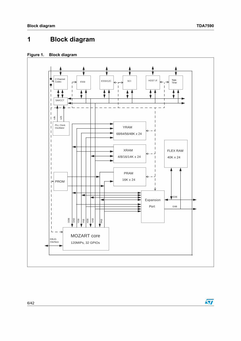
1 Block diagram
Figure 1. Block diagram
MOZART core 120MIPs, 32 GPIOs
EBUGInterface
PROM
PRAM
16K x 24
XRAM
4/8/16/14K x 24
YRAM
68/64/56/48K x 24
FLEX RAM
40K x 24
Expansion
Port
PLL ClockOscillator
2 Channel Codec ESSI ESSI/12C SCI HOST i/f Triple
Timer
DD
B
YD
B
DA
B
YAB
XD
B
XA
B
PAB
EDB
EAB
SAI/CCT
rclk
sclk

TDA7590 Pin description
7/42
2 Pin description
2.1 Pin connection
Figure 2. Pin connection (top view)
144 142 140 138
SC
11
136 134 132 130 128 126 124 122 120 118 116 114 112 110143 141 139 137
SC
12
125 121 117 115 109135 133 131 129 127 123 119 113 111
4546
47 49
HR
EQ
51
IOV
SS
53
HA
S
55
HA
8
57
HA
D6
59
HA
D4
61
CO
RE
VS
S
63
HA
D2
65 67
AA
3
69
XT
I
71
PLL_V
DD
HD
S
WE
N
AA
1
BG
48
HA
CK
50
IOV
DD
52
HC
S
54
HA
D7
56
HA
9
68
AA
2
72
PLL_V
SS
IOV
SS
58
HA
D5
60
CO
RE
VD
D
62
HA
D3
64
HA
D1
66 70
HR
W
OE
N
AA
0
SRD1STD1
SRD0
DB6DB5DB4DB3COREVSS
102
COREVSS
101
COREVDD
100999897
AB5
96
AB1
95
AB3
94
AB2
93
IOVSS
COREVDD
DB1DB2
AB19AB18AB17AB16RXD
TXD
108
AB13
107
AB12
106
IOVSS
105
IOVDD
104
AB11
103
AB10
92
IOVDD
91
IOVSS
90
IOVDD
89
NMI
2SC02 3SC01 4
5
IOVDD
6
IOVSS
7
STD0
8
SC10
9
SC00
10
SCLK
36
DE_N
TESTEN
3132333435
11
SCK1
12
SCK0
13
RESET
14
SCANEN
15
COREVDD
16
COREVSS
17
TIO0
18
VSSSUB
19
DACOP
20
REF0
21
CODEC_VDD
22232425DAC126
CODEC_VSS
27DACOM
282930
1
AB15
3738
39 41 4340 42 44
82818079787776757473
888786858483
AB14
XTO
HA
D0
ADC1ADCOMADCOPIOVDDIOVSS
TD
OT
MS
TC
K
TR
ST
NIR
QD
IRQ
CIR
QB
IRQ
AD
B23
DB
22D
B21
DB
15IO
VS
S
IOV
SS
CO
RE
VS
SC
OR
EV
DD
DB
19
DB
18D
B17
DB
16
IOV
DD
DB
20
DB
14D
B13
DB
12D
B11
DB
10D
B9
IOV
SS
IOV
DD
DB
8D
B7
TD
I
EXTDACLK
BR
BB
IOV
DD
AB4
AB6AB7
DB0
AB
0
IOV
DD
AB9AB8

Pin description TDA7590
8/42
2.2 Pin function
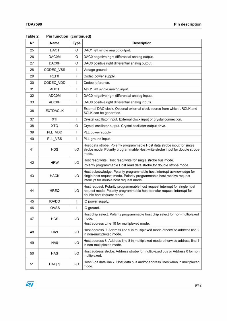
Table 2. Pin function
N° Name Type Description
1 SRD1/TI02 I/O Serial receive data. Serial input data for receiver. Timer 2 input/output.
2 STD1 I/O Serial transmit data. Serial output data from transmitter.
3 SC02 I/OSerial control 2.Transmitter frame sync only in asynchronous mode, transmitter and receiver frame sync in synchronous mode.
4 SC01 I/OSerial control 1. Receive frame sync in asynchronous mode, output
from transmitter 2 or serial flag 1 in synchronous mode.
5 DE_N I/O Test data output (input/output). Debug request input and acknowledge output.
6 NMI_N INon-maskable interrupt/ PINIT. Used to enable the PLL during RESET
and as a non-maskable interrupt at all other times.
7 SRD0 I/O Serial receive data. Serial input data for receiver.
8 IOVDD I IO power supply.
9 IOVSS I IO ground.
10 STD0 I/O Serial Transmit Data. Serial output data from transmitter.
11 SC10/SCL I/OESSI1 serial control 0. Receive clock in asynchronous mode, output from transmitter or serial flag in synchronous mode.
I2C SCL serial clock line.
12 SC00 I/OSerial control 0. Receive clock in asynchronous mode, output from transmitter 1 or serial flag 0 in synchronous mode.
13 RXD I/O SCI receive data. Receives byte-oriented serial data.
14 TXD I/O SCI read enable. Transmits serial data from SCI transmit shift register.
15 SCLK I/OSCI serial clock. Input or output clock from which data is transferred in synchronous mode and from which the transmit and/or receive baud rate is derived in asynchronous mode.
16 SCK1/TI01 I/OSerial clock. Serial bit clock for transmitter only in asynchronous mode, serial bit clock for both receiver and transmitter in synchronous mode.
Timer 1 input/output.
17 SCK0 I/OSerial clock. Serial bit clock for transmitter only in asynchronous mode, serial bit clock for both receiver and transmitter in synchronous mode.
18 RESETN I System reset. A low level applied to RESET_N input initializes the IC.
19 SCANEN ISCAN enable. When active with TESTEN also active, controls the shifting of the internal scan chains.
20 TESTEN ITest enable. When active, puts the chip into test mode and muxes the XTI clock to all flip-flops. When SCANEN is also active, the scan chain shifting is enabled.
21 COREVSS I Core ground.
22 COREVDD I Core power supply.
23 TIO0 I/O Timer 0 input/output.
24 VSSSUB I Analog substrate isolation.
TDA7590 Pin description
9/42
25 DAC1 O DAC1 left single analog output.
26 DAC0M O DAC0 negative right differential analog output.
27 DAC0P O DAC0 positive right differential analog output.
28 CODEC_VSS I Voltage ground.
29 REF0 I Codec power supply.
30 CODEC_VDD I Codec reference.
31 ADC1 I ADC1 left single analog input.
32 ADC0M I DAC0 negative right differential analog inputs.
33 ADC0P I DAC0 positive right differential analog inputs.
36 EXTDACLK IExternal DAC clock. Optional external clock source from which LRCLK and SCLK can be generated.
37 XTI I Crystal oscillator input. External clock input or crystal connection.
38 XTO O Crystal oscillator output. Crystal oscillator output drive.
39 PLL_VDD I PLL power supply.
40 PLL_VSS I PLL ground input.
41 HDS I/OHost data strobe. Polarity programmable Host data strobe input for single strobe mode. Polarity programmable Host write strobe input for double strobe mode.
42 HRW I/OHost read/write. Host read/write for single strobe bus mode.
Polarity programmable Host read data strobe for double strobe mode.
43 HACK I/OHost acknowledge. Polarity programmable host interrupt acknowledge for single host request mode. Polarity programmable host receive request interrupt for double host request mode.
44 HREQ I/OHost request. Polarity programmable host request interrupt for single host request mode. Polarity programmable host transfer request interrupt for double host request mode.
45 IOVDD I IO power supply.
46 IOVSS I IO ground.
47 HCS I/OHost chip select. Polarity programmable host chip select for non-multiplexed mode.
Host address Line 10 for multiplexed mode.
48 HA9 I/OHost address 9. Address line 9 in multiplexed mode otherwise address line 2 in non-multiplexed mode.
49 HA8 I/OHost address 8. Address line 8 in multiplexed mode otherwise address line 1 in non-multiplexed mode.
50 HAS I/OHost address strobe. Address strobe for multiplexed bus or Address 0 for non multiplexed.
51 HAD[7] I/OHost 8-bit data line 7. Host data bus and/or address lines when in multiplexed mode.
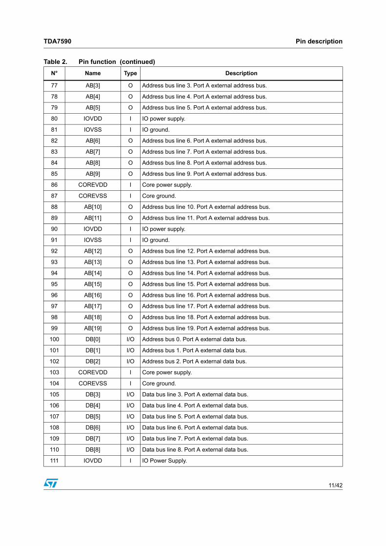
Table 2. Pin function (continued)
N° Name Type Description

Pin description TDA7590
10/42
52 HAD[6] I/OHost 8-bit data line 6. Host data bus and/or address lines when in multiplexed mode.
53 HAD[5] I/OHost 8-bit data line 5. Host data bus and/or address lines when in multiplexed mode.
54 HAD[4] I/OHost 8-bit data line 4. Host data bus and/or address lines when in multiplexed mode.
55 COREVDD I Core power supply.
56 COREVSS I Core ground.
57 HAD[3] I/OHost 8-bit data line 3. Host data bus and/or address lines when in multiplexed mode.
58 HAD[2] I/OHost 8-bit data line 2. Host data bus and/or address lines when in multiplexed mode.
59 HAD[1] I/OHost 8-bit data line 1. Host data bus and/or address lines when in multiplexed mode.
60 HAD[0] I/OHost 8-bit data line 0. Host data bus and/or address lines when in multiplexed mode.
61 AA[3] OAddress attributes line 3.Port A address attributes/chip select pins with programmable polarity.
62 AA[2] OAddress attributes line 2.Port A address attributes/chip select pins with programmable polarity.
63 BR_N OBus request. Asserted when port A requires bus mastership to perform off-chip accesses.
64 BB_N I/OBus busy. Asserted by port A when bus_busy_in_n is negated and BG_N is asserted.
65 IOVDD I IO power supply.
66 IOVSS I IO ground.
67 WEN_N O Write enable.
68 OEN_N O Output enable.
69 AA[1] OAddress attributes line 1.Port A address attributes/chip select pins with programmable polarity.
70 AA[0] OAddress attributes line 0.Port A address attributes/chip select pins with programmable polarity.
71 BG_N IBus grant. When asserted, Port A becomes the bus master elect. Bus mastership
is attained when bus busy is negated by the current bus master.
72 AB[0] O Address bus line 0. Port A external address bus.
73 AB[1] O Address bus line 1. Port A external address bus.
74 IOVDD I IO power supply.
75 IOVSS I IO ground.
76 AB[2] O Address bus line 2. Port A external address bus.
Table 2. Pin function (continued)
N° Name Type Description
TDA7590 Pin description
11/42
77 AB[3] O Address bus line 3. Port A external address bus.
78 AB[4] O Address bus line 4. Port A external address bus.
79 AB[5] O Address bus line 5. Port A external address bus.
80 IOVDD I IO power supply.
81 IOVSS I IO ground.
82 AB[6] O Address bus line 6. Port A external address bus.
83 AB[7] O Address bus line 7. Port A external address bus.
84 AB[8] O Address bus line 8. Port A external address bus.
85 AB[9] O Address bus line 9. Port A external address bus.
86 COREVDD I Core power supply.
87 COREVSS I Core ground.
88 AB[10] O Address bus line 10. Port A external address bus.
89 AB[11] O Address bus line 11. Port A external address bus.
90 IOVDD I IO power supply.
91 IOVSS I IO ground.
92 AB[12] O Address bus line 12. Port A external address bus.
93 AB[13] O Address bus line 13. Port A external address bus.
94 AB[14] O Address bus line 14. Port A external address bus.
95 AB[15] O Address bus line 15. Port A external address bus.
96 AB[16] O Address bus line 16. Port A external address bus.
97 AB[17] O Address bus line 17. Port A external address bus.
98 AB[18] O Address bus line 18. Port A external address bus.
99 AB[19] O Address bus line 19. Port A external address bus.
100 DB[0] I/O Address bus 0. Port A external data bus.
101 DB[1] I/O Address bus 1. Port A external data bus.
102 DB[2] I/O Address bus 2. Port A external data bus.
103 COREVDD I Core power supply.
104 COREVSS I Core ground.
105 DB[3] I/O Data bus line 3. Port A external data bus.
106 DB[4] I/O Data bus line 4. Port A external data bus.
107 DB[5] I/O Data bus line 5. Port A external data bus.
108 DB[6] I/O Data bus line 6. Port A external data bus.
109 DB[7] I/O Data bus line 7. Port A external data bus.
110 DB[8] I/O Data bus line 8. Port A external data bus.
111 IOVDD I IO Power Supply.
Table 2. Pin function (continued)
N° Name Type Description

Pin description TDA7590
12/42
112 IOVSS I IO Ground.
113 DB[9] I/O Data Bus line 9. Port A external data bus.
114 DB[10] I/O Data bus line 10. Port A external data bus.
115 DB[11] I/O Data bus line 11. Port A external data bus.
116 DB[12] I/O Data bus line 12. Port A external data bus.
117 DB[13] I/O Data bus line 13. Port A external data bus.
118 DB[14] I/O Data bus line 14. Port A external data bus.
119 IOVDD I IO power supply.
120 IOVSS I IO Ground.
121 DB[15] I/O Data bus line 15. port a external data bus.
122 DB[16] I/O Data bus line 16. Port A external data bus.
123 DB[17] I/O Data bus line 17. Port A external data bus.
124 DB[18] I/O Data bus line 18. Port A external data bus.
125 DB[19] I/O Data bus line 19. Port A external data bus.
126 COREVDD I Core power supply.
127 COREVSS I Core ground.
128 DB[20] I/O Data bus line 20. Port A external data bus.
129 IOVDD I IO power supply.
130 IOVSS I IO ground.
131 DB[21] I/O Data bus line 21. Port A external data bus.
132 DB[22] I/O Data bus line 22. Port A external data bus.
133 DB[23] I/O Data bus line 23. Port A external data bus.
134 IRQA IInterrupt request line/ Mode control. Used as mode control during RESET and as interrupt request line at all other times.
135 IRQB IInterrupt request line/ Mode control. Used as mode control during RESET and as interrupt request line at all other times.
136 IRQC IInterrupt request line/ Mode control. Used as mode control during RESET and as interrupt request line at all other times.
137 IRQD IInterrupt request line/ Mode control. Used as mode control during RESET and as interrupt request line at all other times.
138 TRSTN I Test reset. JTAG output pin for serial data out from debug interface.
139 TDI I Test data input. JTAG input pin for serial data input for debug interface.
140 TCK I Test clock. JTAG input pin for clocking debug interface.
141 TMS ITest mode select. JTAG input pin for control of TAP Controller of debug interface.
142 TDO O Test data output. JTAG output pin for serial data out from debug interface.
Table 2. Pin function (continued)
N° Name Type Description

TDA7590 Pin description
13/42
2.3 Thermal data
143 SC12 I/OSerial control 2.Transmitter frame sync only in asynchronous mode,
transmitter and receiver frame sync in synchronous mode.
144 SC11/SDA I/O
Serial control 1. Receive frame sync in asynchronous mode,
output from transmitter 2 or serial flag 1 in synchronous mode.
I2C SDA. Serial data line.
Table 2. Pin function (continued)
N° Name Type Description
Table 3. Thermal data
Symbol Parameter Value Unit
Rth-j-pins Thermal resistance junction to pins 32 °C/W

Key parameters TDA7590
14/42
3 Key parameters
3.1 Power consumption
Power consumption depends on application running and DSP clock frequency.
Supply current values are measured and guaranteed at testing level by adopting the benchmarking program reported in Appendix 1.
Table 4. Key parameters
Symbol Parameter Min. Typ. Max. Unit
General
fosc Crystal frequency 16 MHz
CORE_VDD Operating voltage 1.62 1.8 1.98 V
CODEC_VDD Operating voltage 3.0 3.3 3.6 V
IOVDD Operating voltage 3.0 3.3 3.6 V
PLL_VDD Operating voltage 3.0 3.3 3.6 V
IDD_1.8V Supply current 150 mA
IDD_3.3V Supply current 50 mA
Tamb Operating temperature -40 85 °C
DSP core
fdsp DSP clock frequency 120 MHz
ADC single ended
Vpp Maximum input range at ADC1 1.4 V
THD/S Total harmonics distortion to signal -71 dB
(THD+N)/S (THD + Noise) to signal -70 dB
DR Dynamic range 75 dB
ICL Interchannel Isolation -100 dB
ADC differential
Vpp Maximum input range at ADC0M-ADC0P 2.8 V
THD/S Total harmonics distortion to signal -65 dB
(THD+N)/S (THD + Noise) to signal -65 dB
DR Dynamic range 84 dB
ICL Interchannel isolation -100 dB
DAC single ended
Vpp Maximum input range at ADC1 1.4 V
THD/S Total harmonics distortion to signal -64 dB
(THD+N) (THD + Noise) to signal -60 dB

TDA7590 Key parameters
15/42
3.1.1 CODEC (ADC/DAC) test description
Reported typical values (table 3. - ADC and DAC sections) have been measured at Lab level during product evaluation phase. General definitions and procedures are separately defined in following dedicated paragraphs.
Total harmonic distortion with noise to signal (THD+N)/S
THD+N is defined as the ratio of the total power of the second power and higher harmonic with noise components to the power of the fundamental for that signal. For THD+N measurement, choose the DSP analyzer in digital analyzer with THD ratio as measurement option. Measure the THD+N value at -3 dB amplitude of the input signal. First measure the THD+N value at 1Vrms which is 0 dB reference and then measure the value at -3 dB reference.
Dynamic range (DR)
DR is defined as the level of THD+N measured when the input sine wave amplitude is so small that no harmonics apart from the fundamental tone are present in the output signal. This way THD+N becomes practically the ratio between the whole signal and noise floor, being a different way to express SNR. As a convention, at which no harmonics should be present in the output signal, it is fixed at -40dB of the full scale amplitude.
Crosstalk or interchannel isolation
A disturbance, caused by electromagnetic interference, along a circuit or a cable pair. An electric signal disrupts another signal in an adjacent circuit and can cause it to become confused and cross over each other. Crosstalk is measured by applying a signal -3dB amplitude of input signal at one channel (A) and no signal at an other channel (B), measuring the effect on this channel (B) because of the channel (A).
Total harmonic distortion to signal (THD)/S
THD is defined as the ratio of the sum of only those components of the output signal which are harmonic of system input, after having removed the fundamental tone corresponding to the pure sine wave as input and the input signal.This measurement is done by using the Harmonic analyzer which can isolate up to 15th harmonic components on the acquired signal and report the sum of all of them, centering the fundamental tone on the frequency provided by the input signal generator. These measurements are performed at -3dB reference amplitude of input signal.
DR Dynamic range 89 dB
ICL Interchannel isolation -100 dB
DAC differential
Vpp Maximum input range at ADC1 2.8 V
THD/S Total harmonics distortion to signal -58 dB
(THD+N)/S (THD + Noise) to signal -57 dB
DR Dynamic range 90 dB
ICL Interchannel Isolation -85 dB
Table 4. Key parameters (continued)
Symbol Parameter Min. Typ. Max. Unit

Electrical specification TDA7590
16/42
4 Electrical specification
4.1 Absolute maximum ratings
4.2 Electrical characteristics for I/O pins
Table 5. Absolute maximum ratings
Symbol Parameter Value Unit
PLL_VDD 3.3V PLL power supply voltage -0.5 to 4 V
CODEC_VDD 3.3V CODEC analog power supply -0.5 to 4 V
IOVDD 3.3V IO power supply -0.5 to 4 V
CORE_VDD 1.8V CORE power supply -0.5 to 2.2 V
IO_MAX Input or output voltage -0.5 to (IOVDD +0.5) V
Table 6. Recommended DC operating conditions
Symbol Parameter Value Unit
IOVDD IO power supply voltage 3 to 3.6(1) V
Tj Operating junction temperature -40 to 105 °C
1. All the specification are valid only within these recommended operating conditions.
Table 7. General interface electrical characteristics
Symbol Parameter Test condition Min. Typ. Max. Unit
IilLow level input current without pull-up device
1 A
IihHigh level input current without pull-down device
1 A
IozTri-state output leakage without pull up/down device
1 A
IozFTFive Volt tolerant tri-state output leakage without pull up/down device
1 A
I latch-up I/O latch-up current V < 0V, V < Vdd 200 mA
Vesd Electrostatic protection (HBM) leakage < 1mA 2000 V
Vil Low level input voltage(1)) 0.8 V
Vih High level input voltage(1) 2 V
Vhyst Schmitt trigger hysteresis(1) 0.4 V
Vol Low level output voltage (1) (2) (3) Iol = XmA 0.15 V
VohHigh level output voltage (1) (2)
(3) Ioh = -XmA
IOVDD - 0.15
V
1. TTL specifications only apply to the supply voltage range Vdd = 3.15V to 3.6V.
2. Takes into account 200mV voltage drop in both supply lines.
3. X is the source/sink current under worst case conditions and is reflected in the name of the I/O cell according to the drive capability.

TDA7590 24 bit DSP core
17/42
5 24 bit DSP core
The DSP core is a general purpose 24-bit DSP. The main feature of the DSP core are listed below:
• 120 MHz operating frequency (120 MIPS)
• Fully pipelined 24 x 24 bit parallel multiplier-accumulator
• Saturation/limiting logic
• 56-bit parallel barrel shifter
• Linear, reverse carry and modulo addressing modes
• 24-bit address buses for program, X and Y data spaces and DMA
• Memory-expandible hardware stack
• Nested zero-overhead DO loops
• Fast interrupts
• Powerful JTAG emulation port
• Software wait and stop low power standby modes
• Program address tracing support
• Two 24-bit data moves in parallel with arithmetic operations
• External interrupts including non-maskable interrupt
• Interrupts may be independently masked and prioritized
• Bit-manipulation instructions can access any register or memory location
• On board support for DMA controller

Memories TDA7590
18/42
6 Memories
128 K x 24-bit RAM divided into 4 areas, program RAM(PRAM), X data RAM(XRAM), Y data RAM(YRAM) and flexible allocation RAM(FLEX) as follows:
• 16 kB PRAM
• 40 kB FLEX RAM. FLEX RAM is accessed through the expansion port by the DSP core.
• External access to the FLEX RAM is also supported.
• 72 kB RAM is allocated as XRAM and YRAM. Four configurations are supported:
– 4 kB XRAM and 68 kB YRAM
– 8 kB XRAM and 64 kB YRAM
– 16 kB XRAM and 56 kB YRAM
– 24 kB XRAM and 48 kB YRAM
TDA7590 DSP peripherals
19/42
7 DSP peripherals
7.1 Serial audio interface (SAI)
The SAI is used to communicate between the CODEC and the DSPs.
In addition, digital audio can be directly input for processing. There is only one SAI found on the chip that can be accessed by either the DSP or the DMA controller. The main features of this block are listed below:
– Slave operating modes, all clock lines can be inputs or outputs
– Transmit and receive interrupt logic triggers on left/right data pairs
– Receive and transmit data registers have two locations to hold left and right data
7.2 Serial communication interface (SCI)
The serial communication interface provides a full duplex port for serial communication to other DSPs, microprocessors, and peripherals like modems.
The interface supports the following features:
– No additional logic for connection to other TTL level peripherals
– Asynchronous bit rates and protocols "High speed“ synchronous data transmission.
– Asynchronous protocol includes Multidrop mode for master/slave operation with wake-up on Idle line and wake-up on address bit capability, permitting the SCI to share a single line with multiple peripherals
– Transmit and receive logic can operate asynchronously from each other.
– A programmable baud-rate generator which provide the transmit and receive clocks or functions as a general purpose timer.
7.3 I2C interface
The inter integrated-circuit bus is a simple bi-directional two-wire bus used for efficient inter IC control. All I2C bus compatible devices incorporate an on-chip interface which allows them to communicate directly with each other via the I2C bus.
Every component connected to the I2C bus has it s own unique address whether it is a CPU, memory or some other complex function chip. Each of these chips can act as a receiver and/or transmitter depending on it s functionality.
7.4 Host interface (HI)
The host interface is a system-on-chip module that permits connection to the data bus of a host processor. The HI is capable of driving 16 programmable external pins which can be configured as an 8 bit parallel port for direct connection to a host processor.
DSP peripherals TDA7590
20/42
The key features of the host interface are:
• 8 bit parallel port "Full-duplex" dedicated host register bank
• Dedicated Mozart™ core DSP register core bank.
• Register banks map directly into Mozart X memory space
• 3 transfer modes:
– host command
– Host to Mozart core DSP
– Mozart core DSP to host
• Access protocols:
– Software polled
– Interrupt
– DMA access by the Mozart core DSP core
• 2+ wait states clock cycles per transfer
• Supported instructions:
– Data transfer between Mozart core and external host using Mozart MOVE instruction
– Simple I/O service routine with bit addressing instructions
– IO service using fast interrupts with MOVEP instructions.
7.5 ESSI
The ESSI peripheral enables serial-port communication between the DSP core and external devices including Codecs, DSP, microprocessors. The ESSI is capable of driving 12 programmable external pins which can be configured as GPIO ports C and D or ESSI pins.
The key features of the ESSI are:
• Independent receiver and transmitter
• Synchronous or asynchronous channel modes synchronous. Receiver and transmitter use same clock/sync asynchronous. Receiver and transmitter may use separate clock/sync up to one transmitter enabled in asynchronous channel mode.
• Up to three transmitters enabled in synchronous channel mode.
• Normal mode. One word per period.
• Network mode. Up to 32 words per period.
7.6 EOC
The Salieri extended on-chip memory interface provides access to 40 kB of on-chip memory. The Mozart core will treat this memory as if it were external. Access by off-chip expansion bus masters is permitted. All accesses to the extended on-chip RAM are controlled by the extended on-chip memory control register. This register determines which combinations of the Address attribute pins should be interpreted as accesses to the 40 kB of RAM.

TDA7590 DSP peripherals
21/42
7.7 Timers and watchdog block
The timers and watchdog block consists of a common 21-bit prescaler and three independent and identical general-purpose 24-bit timer/event counters, each with its own register set.
Each timer has the following capabilities:
• Uses internal or external clocking.
• Interrupts the Mozart after a specified number of events (clocks).
• Signals an external device after counting internal events.
• Triggers DMA transfers after a specified number of events (clocks) occurs.
• Connects to the external world through designated pins TIO[0-2] for timers 0-2.
When TIO is configured as an
• Input: timer functions as an external event counter. Timer measures external pulse width/signal period.
• Output: timer functions as a:
– Timer
– Watchdog timer
– Pulse-width modulator.
7.8 PLL
The PLL generates the following clocks:
• DCLK: DSP core clock
• DACLK: ADC and DAC clock
• LRCLK: left/right clock for the SAI and the CODEC
• SCLK: shift serial clock for the SAI and the CODEC
7.9 CODEC cell
The main features of the CODEC cell are listed below:
• 20 bits stereo DAC, and 18 bits ADC
• I2S format
• Oversampling ratio: 512
• Sampling rates of 8 kHz to 48 kHz
The analog interface is in the form of differential signals for each channel. The interface on the digital side has the form of an SAI interface and can interface directly to an SAI channel and then to the DSP core.
DCLK can be supplied either by the internal PLL or by external, to allow synchronization with external anal digital sources.

Package information TDA7590
22/42
8 Package information
In order to meet environmental requirements, ST offers these devices in different grades of ECOPACK® packages, depending on their level of environmental compliance. ECOPACK®
specifications, grade definitions and product status are available at: www.st.com.
ECOPACK® is an ST trademark.
Figure 3. TQFP144 mechanical data and package dimensions
OUTLINE ANDMECHANICAL DATA
DIM.mm inch
MIN. TYP. MAX. MIN. TYP. MAX.
A 1.20 0.047
A1 0.05 0.15 0.002 0.006
A2 0.95 1.00 1.05 0.037 0.039 0.041
B 0.17 0.22 0.27 0.007 0.009 0.011
C 0.09 0.20 0.003 0.008
D 21.80 22.00 22.20 0.858 0.866 0.874
D1 19.80 20.00 20.20 0.779 0.787 0.795
D2 2.00 0.079
D3 17.50 0.689
E 21.80 22.00 22.20 0.858 0.866 0.874
E1 19.80 20.00 20.20 0.779 0.787 0.795
E2 2.00 0.079
E3 17.50 0.689
e 0.50 0.020
L 0.45 0.60 0.75 0.018 0.024 0.030
L1 1.00 0.0393
K 0˚ (min.), 3.5˚ (typ.), 7˚(max.)
ccc 0.08 0.03
TQFP144(20x20x1.0mm exposed pad down)
7386636 B
Note 1: Exact shape of each corner is optional.

TDA7590 Appendix 1
23/42
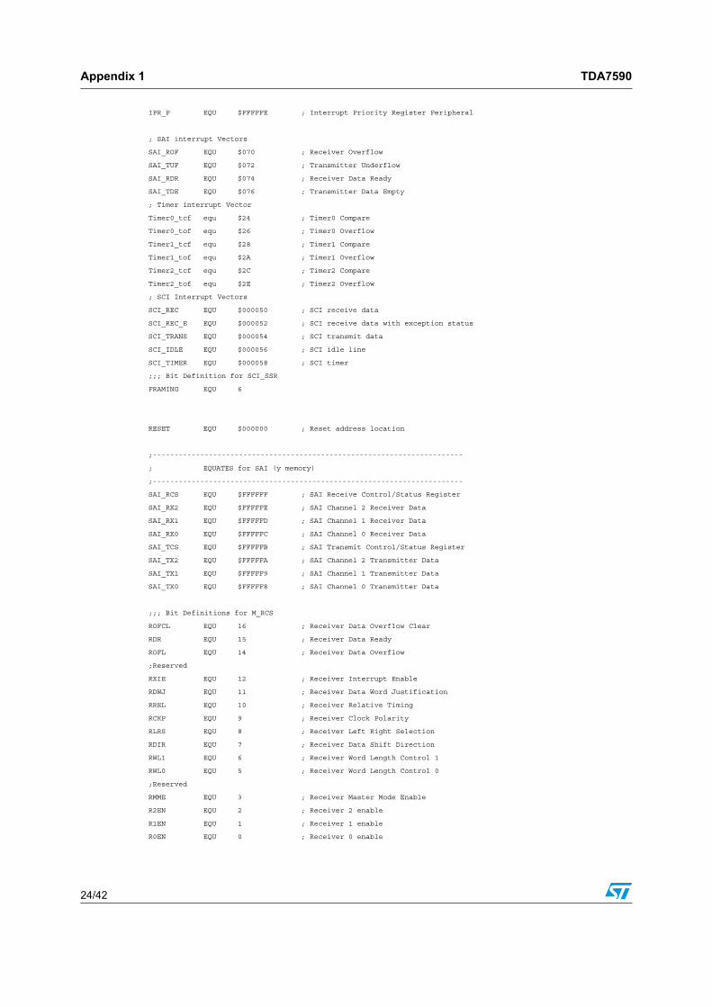
9 Appendix 1
9.1 Benchmarking program;********************************* FILE HEADER *********************************
;
;Title: Salieri CODEC/SAI Functionality Test
;
;File Name: full_func.asm
;
;Author: --
;
;Language: DSP2420 Core Assembler
;
;Project: Salieri
;
;Description: CODEC + TIMER + HI gpios + ESSI + SCI
;
;
;
;
;
;
;
;;
;*******************************************************************************
;*********************************** Equates ***********************************
;*******************************************************************************
Npts equ 20
Ntaps equ 4
;------------------------------------------------------------------------
; EQUATES for I/O Port Programming
;------------------------------------------------------------------------
; Register Addresses
M_HDR EQU $FFFFC9 ; PS- Host port GPIO data Register
M_HDDR EQU $FFFFC8 ; PS- Host port GPIO direction Register
M_PCRC EQU $FFFFBF ; Port C Control Register
M_PRRC EQU $FFFFBE ; Port C Direction Register
M_PDRC EQU $FFFFBD ; Port C GPIO Data Register
M_PCRD EQU $FFFFAF ; Port D Control register
M_PRRD EQU $FFFFAE ; Port D Direction Data Register
M_PDRD EQU $FFFFAD ; Port D GPIO Data Register
M_PCRE EQU $FFFF9F ; Port E Control register
M_PRRE EQU $FFFF9E ; Port E Direction Register
M_PDRE EQU $FFFF9D ; Port E Data Register
M_OGDB EQU $FFFFFC ; OnCE GDB Register
;------------------------------------------------------------------------
; EQUATES for Exception Processing
;------------------------------------------------------------------------
; Register Addresses
IPR_C EQU $FFFFFF ; Interrupt Priority Register Core
Appendix 1 TDA7590
24/42
IPR_P EQU $FFFFFE ; Interrupt Priority Register Peripheral
; SAI interrupt Vectors
SAI_ROF EQU $070 ; Receiver Overflow
SAI_TUF EQU $072 ; Transmitter Underflow
SAI_RDR EQU $074 ; Receiver Data Ready
SAI_TDE EQU $076 ; Transmitter Data Empty
; Timer interrupt Vector
Timer0_tcf equ $24 ; Timer0 Compare
Timer0_tof equ $26 ; Timer0 Overflow
Timer1_tcf equ $28 ; Timer1 Compare
Timer1_tof equ $2A ; Timer1 Overflow
Timer2_tcf equ $2C ; Timer2 Compare
Timer2_tof equ $2E ; Timer2 Overflow
; SCI Interrupt Vectors
SCI_REC EQU $000050 ; SCI receive data
SCI_REC_E EQU $000052 ; SCI receive data with exception status
SCI_TRANS EQU $000054 ; SCI transmit data
SCI_IDLE EQU $000056 ; SCI idle line
SCI_TIMER EQU $000058 ; SCI timer
;;; Bit Definition for SCI_SSR
FRAMING EQU 6
RESET EQU $000000 ; Reset address location
;------------------------------------------------------------------------
; EQUATES for SAI (y memory)
;------------------------------------------------------------------------
SAI_RCS EQU $FFFFFF ; SAI Receive Control/Status Register
SAI_RX2 EQU $FFFFFE ; SAI Channel 2 Receiver Data
SAI_RX1 EQU $FFFFFD ; SAI Channel 1 Receiver Data
SAI_RX0 EQU $FFFFFC ; SAI Channel 0 Receiver Data
SAI_TCS EQU $FFFFFB ; SAI Transmit Control/Status Register
SAI_TX2 EQU $FFFFFA ; SAI Channel 2 Transmitter Data
SAI_TX1 EQU $FFFFF9 ; SAI Channel 1 Transmitter Data
SAI_TX0 EQU $FFFFF8 ; SAI Channel 0 Transmitter Data
;;; Bit Definitions for M_RCS
ROFCL EQU 16 ; Receiver Data Overflow Clear
RDR EQU 15 ; Receiver Data Ready
ROFL EQU 14 ; Receiver Data Overflow
;Reserved
RXIE EQU 12 ; Receiver Interrupt Enable
RDWJ EQU 11 ; Receiver Data Word Justification
RREL EQU 10 ; Receiver Relative Timing
RCKP EQU 9 ; Receiver Clock Polarity
RLRS EQU 8 ; Receiver Left Right Selection
RDIR EQU 7 ; Receiver Data Shift Direction
RWL1 EQU 6 ; Receiver Word Length Control 1
RWL0 EQU 5 ; Receiver Word Length Control 0
;Reserved
RMME EQU 3 ; Receiver Master Mode Enable
R2EN EQU 2 ; Receiver 2 enable
R1EN EQU 1 ; Receiver 1 enable
R0EN EQU 0 ; Receiver 0 enable

TDA7590 Appendix 1
25/42
;;; Bit Definitions for M_TCS
TUFCL EQU 16 ; Transmitter Data Overflow Clear
TDE EQU 15 ; Transmitter Data Ready
TUFL EQU 14 ; Transmitter Data Overflow
;Reserved
TXIE EQU 12 ; Transmitter Interrupt Enable
TDWE EQU 11 ; Transmitter Data Word Justification
TREL EQU 10 ; Transmitter Relative Timing
TCKP EQU 9 ; Transmitter Clock Polarity
TLRS EQU 8 ; Transmitter Left Right Selection
TDIR EQU 7 ; Transmitter Data Shift Direction
TWL1 EQU 6 ; Transmitter Word Length Control 1
TWL0 EQU 5 ; Transmitter Word Length Control 0
;Reserved
TMME EQU 3 ; Transmitter Master Mode Enable
T2EN EQU 2 ; Transmitter 2 enable
T1EN EQU 1 ; Transmitter 1 enable
T0EN EQU 0 ; Transmitter 0 enable
;------------------------------------------------------------------------
; EQUATES for CODEC
;------------------------------------------------------------------------
CODEC_CSR EQU $FFFFCB ; CODEC Control Register Address
;;; Bit Definitions for CODEC
GADCL_0 EQU 0 ; ADC Left Gain Bit 0
GADCL_1 EQU 1 ; ADC Left Gain Bit 1
GADCL_2 EQU 2 ; ADC Left Gain Bit 2
GADCR_0 EQU 3 ; ADC Right Gain Bit 0
GADCR_1 EQU 4 ; ADC Right Gain Bit 1
GADCR_2 EQU 5 ; ADC Right Gain Bit 2
GDACL_0 EQU 6 ; DAC Left Gain Bit 0
GDACL_1 EQU 7 ; DAC Left Gain Bit 1
GDACL_2 EQU 8 ; DAC Left Gain Bit 2
GDACR_0 EQU 9 ; DAC Right Gain Bit 0
GDACR_1 EQU 10 ; DAC Right Gain Bit 1
GDACR_2 EQU 11 ; DAC Right Gain Bit 2
MUTEDAC EQU 12 ; Mute DAC - Active Hi, Reset Val = 1
PDNDAC EQU 13 ; Power down DAC - Active Hi, Reset Val = 0
PDNADC EQU 14 ; Power down ADC - Active Hi, Reset Val = 0
N_RST EQU 15 ; Asynchronoue Reset - Active Lo, Reset Val = 1
;------------------------------------------------------------------------
; EQUATES for PLL
;------------------------------------------------------------------------
PLL_CSR EQU $FFFFD7 ; PLL Control/Status Register
PLL_FCR EQU $FFFFD6 ; PLL Fractional Register
PLL_CLKCTL EQU $FFFFD5 ; PLL Clock Control Register
;;; Bit Definitions for PLL_CSR
IDF0 EQU 0 ; Input Divide Factor 0
IDF1 EQU 1 ; Input Divide Factor 1
IDF2 EQU 2 ; Input Divide Factor 2
IDF3 EQU 3 ; Input Divide Factor 3
IDF4 EQU 4 ; Input Divide Factor 4
; Reserved

Appendix 1 TDA7590
26/42
LOCK EQU 6 ; PLL Lock Indication bit
OUTLOCK EQU 7 ; PLL Lost Lock bit
MF0 EQU 8 ; Multiplication bit 0
MF1 EQU 9 ; Multiplication bit 1
MF2 EQU 10 ; Multiplication bit 2
MF3 EQU 11 ; Multiplication bit 3
MF4 EQU 12 ; Multiplication bit 4
MF5 EQU 13 ; Multiplication bit 5
MF6 EQU 14 ; Multiplication bit 6
PLLIE EQU 15 ; PLL interrupt enable
PWRDN EQU 16 ; PLL power down
DITEN EQU 17 ; Dither Enable
FRACEN EQU 18 ; PLL Fractional-N function enable
PEN EQU 19 ; PLL Enable
;;; Bit Definitions for PLL_CLKCNTL
DSPDF0 EQU 0 ; DSP clock divider factor 0
DSPDF1 EQU 1 ; DSP clock divider factor 1
DSPDF2 EQU 2 ; DSP clock divider factor 2
DSPDF3 EQU 3 ; DSP clock divider factor 3
; Reserved
DCKSRC EQU 6 ; DSP clock source 0->XTI/(DSPDF3:0 + 1)
; 1->VCO/(DSPDF3:0 + 1)
DACLKEN EQU 7 ; Enable bit for oversampling clock
MFSDF0 EQU 8 ; Oversampling multiple bit 0
MFSDF1 EQU 9 ; Oversampling multiple bit 1
MFSDF2 EQU 10 ; Oversampling multiple bit 2
MFSDF3 EQU 11 ; Oversampling multiple bit 3
MFSDF4 EQU 12 ; Oversampling multiple bit 4
MFSDF5 EQU 13 ; Oversampling multiple bit 5
MFSDF6 EQU 14 ; Oversampling multiple bit 6
SEL0 EQU 15 ; Sampling multiple select bit 0
SEL1 EQU 16 ; Sampling multiple select bit 1
SEL2 EQU 17 ; Sampling multiple select bit 2
DSP_XTI EQU 18 ; DSP_XTI =0 -> Use VCO/DSPDF for DCLK
; DSP_XTI =1 -> Use XTI for DCLK
DAC_SEL EQU 19 ; Selects between VCO and ext_dac_clk
XTLD EQU 20 ; Disables the external crystal when set
;------------------------------------------------------------------------
; EQUATES for I/O Port Programming
;------------------------------------------------------------------------
; Register Addresses
HDR EQU $FFFFC9 ; PS- Host port GPIO data Register
HDDR EQU $FFFFC8 ; PS- Host port GPIO direction Register
PCRC EQU $FFFFBF ; Port C Control Register
PRRC EQU $FFFFBE ; Port C Direction Register
PDRC EQU $FFFFBD ; Port C GPIO Data Register
PCRD EQU $FFFFAF ; Port D Control register
PRRD EQU $FFFFAE ; Port D Direction Data Register
PDRD EQU $FFFFAD ; Port D GPIO Data Register
PCRE EQU $FFFF9F ; Port E Control register
PRRE EQU $FFFF9E ; Port E Direction Register
PDRE EQU $FFFF9D ; Port E Data Register
OGDB EQU $FFFFFC ; OnCE GDB Register
TDA7590 Appendix 1
27/42
;------------------------------------------------------------------------
; EQUATES for GPIOs
;------------------------------------------------------------------------
;;; Register Addresses
GPIOCTRL EQU $FFFFc4 ; Host Port Control Register
GPIODIR EQU $FFFFc8 ; GPIODIR register.(HI - HDDR)
GPIODAT EQU $FFFFc9 ; GPIODAT register.(HI - HDR)
;;; Bit Definitions for GPIO Direction Register
GPIO0_DIR EQU $0
GPIO1_DIR EQU $1
GPIO2_DIR EQU $2
GPIO3_DIR EQU $3
GPIO4_DIR EQU $4
GPIO5_DIR EQU $5
GPIO6_DIR EQU $6
GPIO7_DIR EQU $7
GPIO8_DIR EQU $8
;;; Bit Definitions for GPIO Data Register
GPIO0_DAT EQU $0
GPIO1_DAT EQU $1
GPIO2_DAT EQU $2
GPIO3_DAT EQU $3
GPIO4_DAT EQU $4
GPIO5_DAT EQU $5
GPIO6_DAT EQU $6
GPIO7_DAT EQU $7
GPIO8_DAT EQU $8
;------------------------------------------------------------------------
; EQUATES for Timer
;------------------------------------------------------------------------
M_TCSR0 EQU $FFFF8F ;Timer 0 Control/Status Register (TCSR0)
M_TLR0 EQU $FFFF8E ;Timer 0 Load Register (TLR0)
M_TCPR0 EQU $FFFF8D ;Timer 0 Compare Register (TCPR0)
M_TCR0 EQU $FFFF8C ;Timer 0 Count Register (TCR0)
M_TCSR1 EQU $FFFF8B ;Timer 1 Control/Status Register (TCSR1)
M_TLR1 EQU $FFFF8A ;Timer 1 Load Register (TLR1)
M_TCPR1 EQU $FFFF89 ;Timer 1 Compare Register (TCPR1)
M_TCR1 EQU $FFFF88 ;Timer 1 Count Register (TCR1)
M_TCSR2 EQU $FFFF87 ;Timer 2 Control/Status Register (TCSR2)
M_TLR2 EQU $FFFF86 ;Timer 2 Load Register (TLR2)
M_TCPR2 EQU $FFFF85 ;Timer 2 Compare Register (TCPR2)
M_TCR2 EQU $FFFF84 ;Timer 2 Count Register (TCR2)
M_TPLR EQU $FFFF83 ;Timer Prescaler Load Register (TPLR)
M_TPCR EQU $FFFF82 ;Timer Prescaler Count Register (TPCR)
;------------------------------------------------------------------------
;
; EQUATES for Enhanced Synchronous Serial Interface (ESSI)
;
;------------------------------------------------------------------------
;ESSI 0 interrupt equates
essi0_rdf equ $30
essi0_roe equ $32
essi0_rls equ $34
Appendix 1 TDA7590
28/42
essi0_tde equ $36
essi0_tue equ $38
essi0_tls equ $3a
;ESSI 1 interrupt equates
essi1_rdf equ $40
essi1_roe equ $42
essi1_rls equ $44
essi1_tde equ $46
essi1_tue equ $48
essi1_tls equ $4a
;Register Addresses of ESSI0
M_TX00 EQU $FFFFBC ; SSI0 Transmit Data Register 0
M_TX01 EQU $FFFFBB ; SSI0 Transmit Data Register 1
M_TX02 EQU $FFFFBA ; SSI0 Transmit Data Register 2
M_TSR0 EQU $FFFFB9 ; SSI0 Time Slot Register
M_RX0 EQU $FFFFB8 ; SSI0 Receive Data Register
M_SSISR0 EQU $FFFFB7 ; SSI0 Status Register
M_CRB0 EQU $FFFFB6 ; SSI0 Control Register B
M_CRA0 EQU $FFFFB5 ; SSI0 Control Register A
M_TSMA0 EQU $FFFFB4 ; SSI0 Transmit Slot Mask Register A
M_TSMB0 EQU $FFFFB3 ; SSI0 Transmit Slot Mask Register B
M_RSMA0 EQU $FFFFB2 ; SSI0 Receive Slot Mask Register A
M_RSMB0 EQU $FFFFB1 ; SSI0 Receive Slot Mask Register B
;Register Addresses of ESSI1
M_TX10 EQU $FFFFAC ; SSI1 Transmit Data Register 0
M_TX11 EQU $FFFFAB ; SSI1 Transmit Data Register 1
M_TX12 EQU $FFFFAA ; SSI1 Transmit Data Register 2
M_TSR1 EQU $FFFFA9 ; SSI1 Time Slot Register
M_RX1 EQU $FFFFA8 ; SSI1 Receive Data Register
M_SSISR1 EQU $FFFFA7 ; SSI1 Status Register
M_CRB1 EQU $FFFFA6 ; SSI1 Control Register B
M_CRA1 EQU $FFFFA5 ; SSI1 Control Register A
M_TSMA1 EQU $FFFFA4 ; SSI1 Transmit Slot Mask Register A
M_TSMB1 EQU $FFFFA3 ; SSI1 Transmit Slot Mask Register B
M_RSMA1 EQU $FFFFA2 ; SSI1 Receive Slot Mask Register A
M_RSMB1 EQU $FFFFA1 ; SSI1 Receive Slot Mask Register B
;------------------------------------------------------------------------
; EQUATES for SCI
;------------------------------------------------------------------------
PCRE_ADR EQU $FFFF9F ; Serial Port Control Register
PRRE_ADR EQU $FFFF9E ; Serial Port Direction Register
PDRE_ADR EQU $FFFF9D ; Serial Port Direction Register
SCR_ADR EQU $FFFF9C ; SCI Control Register
SCCR_ADR EQU $FFFF9B ; SCI Clock Control Register
SRXH_ADR EQU $FFFF9A ; Serial Recieve Register high
SRXM_ADR EQU $FFFF99 ; Serial Recieve Register mid
SRXL_ADR EQU $FFFF98 ; Serial Recieve Register low
STXH_ADR EQU $FFFF97 ; Serial Transmit Register high
STXM_ADR EQU $FFFF96 ; Serial Transmit Register mid
STXL_ADR EQU $FFFF95 ; Serial Transmit Register low
STXA_ADR EQU $FFFF94 ; Serial Transmit Adress Register
SSR_ADR EQU $FFFF93 ; Serial Status Register
TDA7590 Appendix 1
29/42
;------------------------------------------------------------------------
; EQUATES for Expansion Port
;------------------------------------------------------------------------
EXP_BCR EQU $FFFFFB ; Bus Control Register address
EXP_AAR0 EQU $FFFFF9 ; Address Attribte Register (AAR0) address
EXP_AAR1 EQU $FFFFF8 ; Address Attribte Register (AAR1) address
EXP_AAR2 EQU $FFFFF7 ; Address Attribte Register (AAR2) address
EXP_AAR3 EQU $FFFFF6 ; Address Attribte Register (AAR3) address
EXT_RAM_STARTEQU $C00000
;------------------------------------------------------------------------
; EQUATES for Extended Memory
;------------------------------------------------------------------------
EOC_ADR EQU $FFFFCA
;*******************************************************************************
;***************************** Initialisation Values **************************
;*******************************************************************************
;-------------------------------------------------------------------------------
; CODEC Intitialisation values
;-------------------------------------------------------------------------------
; --- INIT_CCR -----------------------------------------------------------------
; settings fro the CODEC Control Register
; 321098765432109876543210
INIT_CODEC_CSR EQU %000000001110011011011011 ; $00E6DB DACgain = 0dB - ADCgain = +0dBdB
; 011 --- GADCL[0:2]
; 011 ------ GADCR[0:2]
; 011 --------- GDACL[0:2]
; 011 ------------ GDACR[0:2]
; 0 --------------- MUTEDAC (1=Mute)
; 1 ---------------- PDNDAC (1=pwrdwn)
; 1 ----------------- PDNADC (1=pwrdwn)
; 1 ------------------ NRST (0=reset)
;-------------------------------------------------------------------------------
; SAI Intitialisation values
;-------------------------------------------------------------------------------
;--- INIT_RCS ------------------------------------------------------------------
; settings for the Receiver Control/Status Register
; 321098765432109876543210
INIT_SAI_RCS EQU %000000000001000101001001 ; $000149
; 1 --- R0EN (0:Disbaled; 1:Enabled)
; 0 ---- R1EN (0:Disbaled; 1:Enabled)
; 0 ----- R2EN (0:Disbaled; 1:Enabled)
; 1 ------ RMME (1:Master mode; 0:Slave mode)
; 0 ------- Reserved
; 10 -------- RWL[0:1] (00:16; 01:24; 10:32)
; 0 ---------- RDIR (0:MSB 1st; 1:LSB 1st)
; 1 ----------- RLRS (0:LRCKR=0-LW; 1:LRCKR=0-RW)
; 0 ------------ RCKP (0:-ve ; 1:+ve)
; 0 ------------- RREL (0:trans-1st; 1:I2S)
; 0 -------------- RDWJ
; 1 --------------- RXIE (0:Disabled; 1:Enabled)
; 0 ---------------- Reserved
; 0 ----------------- ROFL

Appendix 1 TDA7590
30/42
; 0 ------------------ RDR
; 0 ------------------- ROFCL
;--- INIT_TCS ------------------------------------------------------------------
; settings for the Transmitter Control/Status Register
; 321098765432109876543210
INIT_SAI_TCS EQU %000000000001010101001001 ; $000549 - non incrociato
; 1 --- T0EN (0:Disbaled; 1:Enabled)
; 0 ---- T1EN (0:Disbaled; 1:Enabled)
; 0 ----- T2EN (0:Disbaled; 1:Enabled)
; 1 ------ TMME (1:Master mode; 0:Slave mode)
; 0 ------- reserved
; 10 -------- TWL[0:1] (00:16; 01:24; 10:32)
; 0 ---------- TDIR (0:MSB 1st; 1:LSB 1st)
; 1 ----------- TLRS (0:LRCKR=0-LW; 1:LRCKR=0-RW)
; 0 ------------ TCKP (0:-ve ; 1:+ve)
; 1 ------------- TREL (0:trans-1st; 1:I2S)
; 0 -------------- TDWE
; 1 --------------- TXIE (0:Disabled; 1:Enabled)
; 0 ---------------- Reserved
; 0 ----------------- TUFL
; 0 ------------------ TDE
; 0 ------------------- TUFCL
;-------------------------------------------------------------------------------
; PLL Intitialisation values
;-------------------------------------------------------------------------------
IF 1 ; Settings per sci 115200
;--- PLL_CSR -------------------------------------------------------------------
; settings for the PLL control register
; 321098765432109876543210
; settings for the PLL control register
; 321098765432109876543210
;INIT_PLL_CSR EQU $0E0C00
INIT_PLL_CSR EQU %000011100000110000000000 ; $0E0C00
; 00000 --- IDF =0 (actual = IDF+1=1)
; 0 -------- RESERVED
; 0 --------- LOCK (read only; 0:out of lock)
; 0 ---------- OUTLOCK (read only; 0:in lock)
; 0001100 ----------- MF =12 (actual = MF + 1 = 13)
; 0 ------------------ PLLIE (0:intr disable)
; 0 ------------------- PWRDN (1:power down mode)
; 1 -------------------- DITEN (0:disable)
; 1 --------------------- FRACTN (0:disable)
; 1 ---------------------- PEN (1:PLL enable)
;--- FRACT ---------------------------------------------------------------------
; settings for the Fractional N part of the PLL
; 321098765432109876543210
;INIT_PLL_FCR EQU $0034bd
INIT_PLL_FCR EQU %000000000011010010111101 ; $0034bd
; 01110000101001 --- FRACT = 13501
;--- CLKCTL --------------------------------------------------------------------

TDA7590 Appendix 1
31/42
; settings for the clock control register
; 321098765432109876543210
;INIT_PLL_CLKCTL EQU $018cc1
INIT_PLL_CLKCTL EQU %000000011000001011000001 ; $018cc1
; 0001 --- DSPDF =1 (actual = DSPDF+1=3)
; 00 ------- TESTSEL
; 1 --------- DCKSRC (0:XTI; 1:FVCO)
; 1 ---------- DACLKEN (1: enable CODEC clocks)
; 0000010 ----------- MFSDF =2 (actual =MFSDF+1 = 3 )
; 011 ------------------ SEL (000:128,001:256, 010:384, etc)
; 0 --------------------- DSP_XTI (0:vco/DSPDF; 1:xti)
; 0 ---------------------- DAC_SEL (0:vco/MFSDF; 1:ext_dac_clk)
; 0 ----------------------- XTLD (0:Enabled; 1:Disabled)
ENDIF ; Settings per sci 115200
;------------------------------------------------------------------------
; Timer Intitialisation values
;------------------------------------------------------------------------
;--- TCSR0 --------------------------------------------------------------------
; settings for the Timer Control/Status Register
; 321098765432109876543210
INIT_TCSR0 EQU %000000001000101000000100 ; $8A04 mode0 / trm=1 / tce=1 / pce=1/ dir=out
INIT_TCSR1 EQU %000000001000101000000100 ; $8A04 mode0 / trm=1 / tce=1 / pce=1/ dir=out
INIT_TCSR2 EQU %000000001000101000000100 ; $8A04 mode0 / trm=1 / tce=1 / pce=1/ dir=out
; xx ----------------------->[23-22]; unused
; 0 ---------------------->[21] TCF ; Timer Compare Flag
; 0 --------------------->[20] TOF ; Timer Overflow Flag
; xxxx ----------------->[19-16] ; unused
; 0 ---------------->[15] PCE ; Prescaler Clock Enable
; x --------------->[14] ; unused
; 0 -------------->[13] DO ; Data Output
; 0 ------------->[12] DI ; Data Input
; 1 ------------>[11] DIR ; Direction
; x ----------->[10] ; unused
; 1 ---------->[ 9] TRM ; Timer Reload Mode
; 0 --------->[ 8] INV ; Inverter
; 0000 ----->[7-4] Tc[3-0] ; Timer Control = Mode0
; x ---->[ 3] ; unused
; 1 --->[ 2] TCIE ; Timer Compare Interrupt Enable
; 0 -->[ 1] TOIE ; Timer Overflow Enable
; 0 ->[ 0] TE ; Timer Enable
;--- TLR0 --------------------------------------------------------------------
; settings for the Timer Load Register
INIT_TLR0 EQU $000000
INIT_TLR1 EQU $000000
INIT_TLR2 EQU $000000
;--- TCPR0 --------------------------------------------------------------------
; settings for the Timer Compare Register
;INIT_TCPR0 EQU $000002
;INIT_TCPR1 EQU $000004
;INIT_TCPR2 EQU $000008
INIT_TCPR0 EQU $000000
INIT_TCPR1 EQU $000000
Appendix 1 TDA7590
32/42
INIT_TCPR2 EQU $000000
;--- TPLR --------------------------------------------------------------------
; settings for the clock control register
; 321098765432109876543210
;INIT_TPLR EQU %001000000000001111100111 ; $2003E7 source TIO0 / divider = 999+1
INIT_TPLR EQU %000000000000001111100111 ; $0003E7 source internal / prescaler 999
; x------------------------> ; Reserved. Write to zero for future compatibility.
; 01----------------------> PS[1-0] ; Prescaler Source [00 internal / 01 external TIO0 /
; ; 10 external TIO0 / 11 external TIO0]
; 000000000010000000000-> PL[20-0] ; Prescaler Preload Value200400
;-------------------------------------------------------------------------------
; Interrupt Initialisation Values
;-------------------------------------------------------------------------------
; settings for the Interrupt priority register - Core
; 321098765432109876543210
INIT_IPR_C EQU %000000000000000000000000 ; $000000
; settings for the Interrupt priority register - peripherals
; 321098765432109876543210
INIT_IPR_P EQU %000000000011111001000100 ; $29C4 glitch sull'uscita del dac
; 00---- HI
; 11------ ESSI0
; 00-------- ESSI1
; 11---------- SCI
; 11------------ TIMER
; 11 ------------- SAI
; 11 --------------- CODEC
; 00 ----------------- PLL
; 00 ------------------- Unknow
; 00 --------------------- I2C
; 00 ----------------------- SPI
; 00 ------------------------- EMI
;-------------------------------------------------------------------------------
; Expansion Port Intitialisation values
;-------------------------------------------------------------------------------
;--- INIT_AAR0 -----------------------------------------------------------------------
; settings for the Address Attribute Register1
; 321098765432109876543210
INIT_AAR0 EQU %110000000000010000010000 ; C00410
; 00 --- BAT (00: Synchronous SRAM; 01: SRAM; 10: DRAM; 11: Reserved)
; 0 ----- BAAP (0:AA1 active low; 1: AA1 active high)
; 0 ------ BPEN (0: P space disabled; 1: P space enabled)
; 1 ------- BXEN (0: X data space disabled; 1: X data space enabled)
; 0 -------- BYEN (0: Y data space disabled; 1: Y data space enabled)
; 0 --------- BAM (0: 8 LSB of address will appear on A0-A7;
; 1: 8 LSB of address will appear on A16-A23)
; 0 ---------- BPAC (0: packing disabled; 1: packing enabled)
; 0100 ----------- BNC (Number of bits to compare; 1111, 1110, 1101 reserved)
; 110000000000 --------------- BAC (Address to compare; BNC most significant)
;--- INIT_BCR -----------------------------------------------------------------------

TDA7590 Appendix 1
33/42
; settings for the Bus Control Register
; 321098765432109876543210
INIT_BCR EQU %001100000010010000100001 ; 306E10
;INIT_BCR EQU %000001111111110011100111 ; 30FE07
; 00111 --- BA0W (Area 0 wait states)
; 00000 -------- BA1W (Area 1 wait states)
; 111 ------------- BA2W (Area 2 wait states)
; 111 ---------------- BA3W (Area 3 wait states)
; 00000 ------------------- BDFW (Default area wait states)
; 0 ------------------------ BBS (0: ; 1: DSP is bus master READ ONLY)
; 0 ------------------------- BLH (0: ; 1: BLN always asserted)
; 0 -------------------------- BRH (0: ; 1: BRN always asserted)
;*******************************************************************************
; definitions addded by Paul Cassidy for salieri testbench
TRIGGER_TUBE EQU $12002
M_BCR EQU $FFFFFB ; Bus Control Register
M_AAR0 EQU $FFFFF9 ; Address Attribute 0
M_AAR1 EQU $FFFFF8 ; Address Attribute 1
M_AAR2 EQU $FFFFF7 ; Address Attribute 2
M_AAR3 EQU $FFFFF6 ; Address Attribute 3
;*******************************************************************************
;************************** Main Prog Starts Here ******************************
;*******************************************************************************
startp
org p:$0
jmp start
sci_int
org p:SCI_REC ; Interrupt SCI receive
jsr INT_SCIR
org p:SCI_TRANS ; Interrupt SCI transmit
jsr INT_SCIT
org p:SCI_REC_E ; Interrupt SCI framing error
jsr INT_SCIE
sai_int
org p:SAI_RDR
jsr INT_RDR
org p:SAI_TDE
jsr INT_TDE
org p:SAI_ROF
jsr INT_ROF
org p:SAI_TUF
jsr INT_TUF
essi_int
org p:essi0_rdf
jsr Comp_0
nop
org p:essi0_roe

Appendix 1 TDA7590
34/42
movep x:M_SSISR0,a0
movep x:M_RX0,y:(r0)+
org p:essi0_rls
nop
nop
org p:essi0_tde
jsr clr_tde0
nop
org p:essi0_tue
jsr clr_tue0
nop
org p:essi0_tls
nop
nop
timer_int
org p:Timer0_tcf
jsr INT_TMR0_tcf
org p:Timer0_tof
jsr INT_TMR0_tof
org p:Timer1_tcf
jsr INT_TMR1_tcf
org p:Timer1_tof
jsr INT_TMR1_tof
org p:Timer2_tcf
jsr INT_TMR2_tcf
org p:Timer2_tof
jsr INT_TMR2_tof
org x:0
states dsm ntaps
org y:0
coef dc .1,.3,-.1,.2
org p:$100
start
; setup external memory for sync with testbench
;------------------------------------------------------------------------
; Initialise Core
;------------------------------------------------------------------------
clr a
clr b
move #$0,r0
move #$fff,m0
ori #$3,mr ; mask interrupts
movep #INIT_IPR_C,x:IPR_C ; set CORE interrupt priorities
movep #INIT_IPR_P,x:IPR_P ; set PERIPHERAL interrupt priorities
;------------------------------------------------------------------------
; Initialise PLL
;------------------------------------------------------------------------
init_pll
movep #INIT_PLL_CSR,x:PLL_CSR ; enable the pll.
jclr #LOCK,x:<<PLL_CSR,* ; wait for lock.

TDA7590 Appendix 1
35/42
movep #INIT_PLL_FCR,x:PLL_FCR ; set fract value.
bset #FRACEN,x:<<PLL_CSR ; enable fractional-n operation.
movep #INIT_PLL_CLKCTL,x:PLL_CLKCTL ; setup the clock generation.
IF 1
;------------------------------------------------------------------------
; Initialise CODEC
;------------------------------------------------------------------------
init_codec
movep #INIT_CODEC_CSR,x:CODEC_CSR ; initialise CODEC control/status reg
;------------------------------------------------------------------------
; Initialise SAI
;------------------------------------------------------------------------
; The receiver and transmitter control/status register are configured the same for simplicity only.
; Master mode , 24-bit word-size , MSB first , Low word clock = left word , Neg bit-clk polarity ,
; Non i2s format , (For 32-bit words) First bit x 8 , Interrupts enabled.
init_sai
movep #INIT_SAI_TCS,y:SAI_TCS ; initialise transmit control/status reg
movep #INIT_SAI_RCS,y:SAI_RCS ; initialise receiver control/status reg
;------------------------------------------------------------------------
; Enable gpios for HI
;------------------------------------------------------------------------
bset #GPIO0_DIR,x:GPIOCTRL ; Setup HI pin for GPIO mode
bset #GPIO0_DIR,x:GPIODIR ; Setup GPIO as output
bset #GPIO1_DIR,x:GPIOCTRL ; Setup HI pin for GPIO mode
bset #GPIO1_DIR,x:GPIODIR ; Setup GPIO as output
ENDIF
;------------------------------------------------------------------------
; Initialize ESSI0
;------------------------------------------------------------------------
IF 1
init_essi
movep #$181801,x:M_CRA0 ; cra0_addr, 24'b010110000001100000011110
; The divider control is set to 1 (2 words per frame)
; for Normal mode, bits are left aligned to bit 23. Word
; length is set to 24 bits.PM = 1 -> Fcore/4.
movep #$fc113e,x:M_CRB0 ; crb0_addr, 24'b111111000001010100111110
; The receive exception and transmit exception interrupts
; are enabled as are receive last slot and transmit last
; slot. It is set in the synchronous normal mode. Data and
; frame sync are clocked out on the rising edge of the clock.
; Frame sync polarity is positive and occurs together with the
; the first bit of data from the first slot. MSB is shifted
; first. SC2 o/p SC1 o/p SC0 o/p
Enable_pins
;------------------------------------------------------------------------
move #$01c000,x0 ;
movep x:M_CRB0,b1 ;
or x0,b1 ; // Enable TX2/TX1/TX0 (ESSI 0)
movep #$00003f,x:M_PCRC ; // ALL Pins are ESSI.
; check that all pins are enabled
rep #$05
nop

Appendix 1 TDA7590
36/42
movep b1,x:M_CRB0
ENDIF
IF 1
;------------------------------------------------------------------------
; Enable gpios for TIMER
;------------------------------------------------------------------------
init_gpio
; movep #$000000,x:<<PCRC ; ESSI0 port as GPIO
; movep #$0000ff,x:<<PRRC ; ESSI0 port as OUT
Movep #$000000,x:<<PCRD ; ESSI1 port as GPIO
Movep #$000000,x:<<PRRD ; ESSI1 port as TIMER(INPUT)
;------------------------------------------------------------------------
; Initialise Timer
;------------------------------------------------------------------------
init_timer
bclr #0,x:M_TCSR0 ; Disable Timer0
bclr #0,x:M_TCSR1 ; Disable Timer1
bclr #0,x:M_TCSR2 ; Disable Timer2
movep #INIT_TCSR0,x:<<M_TCSR0 ; Timer0 enable at mode 0 + reload
movep #INIT_TPLR,x:<<M_TPLR ; Initial value of the timer counter
movep #INIT_TLR0,x:<<M_TLR0 ; Initial value of the timer counter
movep #INIT_TCPR0,x:<<M_TCPR0 ; Number of CLK/2 cycles until a trigger is generated
movep #INIT_TCSR1,x:<<M_TCSR1 ; Timer1 enable at mode 0 + reload
movep #INIT_TPLR,x:<<M_TPLR ; Initial value of the timer counter
movep #INIT_TLR1,x:<<M_TLR1 ; Initial value of the timer counter
movep #INIT_TCPR1,x:<<M_TCPR1 ; Number of CLK/2 cycles until a trigger is generated
movep #INIT_TCSR2,x:<<M_TCSR2 ; Timer2 enable at mode 0 + reload
movep #INIT_TPLR,x:<<M_TPLR ; Initial value of the timer counter
movep #INIT_TLR2,x:<<M_TLR2 ; Initial value of the timer counter
movep #INIT_TCPR2,x:<<M_TCPR2 ; Number of CLK/2 cycles until a trigger is generated
;------------------------------------------------------------------------
; Initialise Expansion Port and Flex Memory
;------------------------------------------------------------------------
init_expport
movep #INIT_AAR0,x:EXP_AAR0 ; initialise AAR0 control/status reg
movep #INIT_BCR,x:EXP_BCR ; initialise BCR reg
ENDIF
;------------------------------------------------------------------------
; Initialise SCI
;------------------------------------------------------------------------
IF 1
init_sci
movep #$E,x:SCCR_ADR
movep #$7,x:PCRE_ADR
movep #$11b02,x:SCR_ADR

TDA7590 Appendix 1
37/42
ENDIF
;------------------------------------------------------------------------
; Enable interrupts
;------------------------------------------------------------------------
Andi #$fc,mr ; set DSP interrupt priority level to 0
; Sets the Interrupt Mask bits in the SR
; to [00] (No exceptions masked)
IF 1
Bset #0,x:M_TCSR0 ; Enable Timer0
Bset #0,x:M_TCSR1 ; Enable Timer1
Bset #0,x:M_TCSR2 ; Enable Timer2
ENDIF
move #states,r3
move #ntaps-1,m3
move #coef,r4
move #ntaps-1,m4
;------------------------------------------------------------------------
; Processor Loop
;------------------------------------------------------------------------
IF 0
LOOP
; bset #12,x:SCR_ADR ; start SCI transmit
nop
nop
nop
nop
nop
nop
nop
nop
nop
nop
nop
nop
jmp LOOP
ENDIF
IF 1
LOOP
; bset #12,x:SCR_ADR ; start SCI transmit
mac x0,y0,a x:(r3)+,x0 y:(r4)+,y0 ; generates variations on mean value of DAC
move #$AAAAAA,x0
move x0,x:$CAAAAA ; send data to expansion port
move x0,x:GPIODAT ; move PORTB pins
bset #12,x:SCR_ADR ; start SCI transmit
mac x0,y0,a x:(r3)+,x0 y:(r4)+,y0 ; generates variations on mean value of DAC
move #$555555,x0
move x0,x:$C55555 ; send data to expansion port
move x0,x:GPIODAT ; move PORTB pins

Appendix 1 TDA7590
38/42
bset #12,x:SCR_ADR ; start SCI transmit
mac x0,y0,a x:(r3)+,x0 y:(r4)+,y0 ; generates variations on mean value of DAC
move #$AAAAAA,x0
move x0,x:$CAAAAA ; send data to expansion port
move x0,x:GPIODAT ; move PORTB pins
bset #12,x:SCR_ADR ; start SCI transmit
mac x0,y0,a x:(r3)+,x0 y:(r4)+,y0 ; generates variations on mean value of DAC
move #$555555,x0
move x0,x:$C55555 ; send data to expansion port
move x0,x:GPIODAT ; move PORTB pins
jmp LOOP
ENDIF
;------------------------------------------------------------------------
; Interrupt Service Routines
;------------------------------------------------------------------------
;SAI
;------------------------------------------------------------------------
INT_TDE ; The transmitter data empty flag is cleared as soon
; as the last move is performed
Movep a,y:<<SAI_TX0 ; Load LEFT transmit data register for channel 0
nop
nop
movep b,y:<<SAI_TX0 ; Load RIGHT transmit data register for channel 0
rti
INT_RDR ; The receiver data ready flag is cleared as soon
; as the last move is performed
movep y:<<SAI_RX0,a ; Move Channel 0 received LEFT data to x-memory.
move a,x:(r0)
nop
nop
movep y:<<SAI_RX0,b ; Move channel 0 received RIGHT data to y-memory.
move b,y:(r0)+
rti
INT_ROF
bset #16,y:SAI_RCS
bclr #16,y:SAI_RCS
rti
INT_TUF
bset #16,y:SAI_TCS
bclr #16,y:SAI_RCS
rti
;TIMER

TDA7590 Appendix 1
39/42
;------------------------------------------------------------------------
INT_TMR0_tcf
; bchg #0,x:PDRC ; toggle pin12 Fout=(XTI/2)/((TPLR+1)*(TCPR+1)*2)
bchg #13,x:M_TCSR0 ; toggle TIO0 Fout=(XTI/2)/((TPLR+1)*(TCPR+1)*2)
nop
rti
INT_TMR0_tof
nop
nop
rti
INT_TMR1_tcf
; bchg #1,x:PDRC ; toggle pin4 Fout=Fin/((TPLR+1)*(TCPR+1)*2)
bchg #13,x:M_TCSR1 ; toggle TIO1 Fout=(XTI/2)/((TPLR+1)*(TCPR+1)*2)
nop
rti
INT_TMR1_tof
nop
nop
rti
INT_TMR2_tcf
; bchg #2,x:PDRC ; toggle pin3 Fout=Fin/((TPLR+1)*(TCPR+1)*2)
bchg #13,x:M_TCSR2 ; toggle TIO2 Fout=(XTI/2)/((TPLR+1)*(TCPR+1)*2)
nop
rti
INT_TMR2_tof
nop
nop
rti
;ESSI
;------------------------------------------------------------------------
clr_tde0
movep r1,x:M_TX00
move (r1)+
movep r1,x:M_TX01
move (r1)+
movep r1,x:M_TX02
move (r1)+
rti
clr_tue0
movep x:M_SSISR0,a0
movep r1,x:M_TX00
move (r1)+
movep r1,x:M_TX01
move (r1)+
movep r1,x:M_TX02
move (1)+
rti
Comp_0
rti

Appendix 1 TDA7590
40/42
Clr_gpio
bclr #0,x:M_PDRE
rti
Comp_1
rti
;SCI
;------------------------------------------------------------------------
INT_SCIR
move x:SRXL_ADR,x0
movep #$3f02,x:SCR_ADR
; move x0,x:(r1)+
; move x0,x:$C00000
rti
INT_SCIT
; movep x0,x:STXA_ADR
movep #$000041,x:STXA_ADR
; movep #$000061,x:STXA_ADR
L3
jclr #0,x:<<SSR_ADR,L3
movep #$12f02,x:SCR_ADR
rti
INT_SCIE
jclr #FRAMING,x:SSR_ADR,NO_FRA
L2
jclr #0,x:<<SSR_ADR,L2
movep #$21,x:STXA_ADR
NO_FRA
nop
move x:SRXL_ADR,x0
rti

TDA7590 Revision history
41/42
Revision history
Table 8. Document revision history
Date Revision Changes
11-Apr-2006 1 Initial release.
26-Jan-2009 2Document status promoted from preliminary data to datasheet.
Updated Section 8: Package information on page 22.
23-Sep-2013 3 Updated Disclaimer.

TDA7590
42/42
Please Read Carefully:
Information in this document is provided solely in connection with ST products. STMicroelectronics NV and its subsidiaries (“ST”) reserve theright to make changes, corrections, modifications or improvements, to this document, and the products and services described herein at anytime, without notice.
All ST products are sold pursuant to ST’s terms and conditions of sale.
Purchasers are solely responsible for the choice, selection and use of the ST products and services described herein, and ST assumes noliability whatsoever relating to the choice, selection or use of the ST products and services described herein.
No license, express or implied, by estoppel or otherwise, to any intellectual property rights is granted under this document. If any part of thisdocument refers to any third party products or services it shall not be deemed a license grant by ST for the use of such third party productsor services, or any intellectual property contained therein or considered as a warranty covering the use in any manner whatsoever of suchthird party products or services or any intellectual property contained therein.
UNLESS OTHERWISE SET FORTH IN ST’S TERMS AND CONDITIONS OF SALE ST DISCLAIMS ANY EXPRESS OR IMPLIEDWARRANTY WITH RESPECT TO THE USE AND/OR SALE OF ST PRODUCTS INCLUDING WITHOUT LIMITATION IMPLIEDWARRANTIES OF MERCHANTABILITY, FITNESS FOR A PARTICULAR PURPOSE (AND THEIR EQUIVALENTS UNDER THE LAWSOF ANY JURISDICTION), OR INFRINGEMENT OF ANY PATENT, COPYRIGHT OR OTHER INTELLECTUAL PROPERTY RIGHT.
ST PRODUCTS ARE NOT DESIGNED OR AUTHORIZED FOR USE IN: (A) SAFETY CRITICAL APPLICATIONS SUCH AS LIFESUPPORTING, ACTIVE IMPLANTED DEVICES OR SYSTEMS WITH PRODUCT FUNCTIONAL SAFETY REQUIREMENTS; (B)AERONAUTIC APPLICATIONS; (C) AUTOMOTIVE APPLICATIONS OR ENVIRONMENTS, AND/OR (D) AEROSPACE APPLICATIONSOR ENVIRONMENTS. WHERE ST PRODUCTS ARE NOT DESIGNED FOR SUCH USE, THE PURCHASER SHALL USE PRODUCTS ATPURCHASER’S SOLE RISK, EVEN IF ST HAS BEEN INFORMED IN WRITING OF SUCH USAGE, UNLESS A PRODUCT ISEXPRESSLY DESIGNATED BY ST AS BEING INTENDED FOR “AUTOMOTIVE, AUTOMOTIVE SAFETY OR MEDICAL” INDUSTRYDOMAINS ACCORDING TO ST PRODUCT DESIGN SPECIFICATIONS. PRODUCTS FORMALLY ESCC, QML OR JAN QUALIFIED AREDEEMED SUITABLE FOR USE IN AEROSPACE BY THE CORRESPONDING GOVERNMENTAL AGENCY.
Resale of ST products with provisions different from the statements and/or technical features set forth in this document shall immediately voidany warranty granted by ST for the ST product or service described herein and shall not create or extend in any manner whatsoever, anyliability of ST.
ST and the ST logo are trademarks or registered trademarks of ST in various countries.Information in this document supersedes and replaces all information previously supplied.
The ST logo is a registered trademark of STMicroelectronics. All other names are the property of their respective owners.
© 2013 STMicroelectronics - All rights reserved
STMicroelectronics group of companies
Australia - Belgium - Brazil - Canada - China - Czech Republic - Finland - France - Germany - Hong Kong - India - Israel - Italy - Japan - Malaysia - Malta - Morocco - Philippines - Singapore - Spain - Sweden - Switzerland - United Kingdom - United States of America
www.st.com