Embed Size (px)
Citation preview
This controller datasheet was downloaded from http://www.crystalfontz.com/controllers/Crystalfontz
MP Specifications November 4, 2004 Revision 1.1
ULTRACHIP The Coolest LCD Driver. Ever!!
128COM x 240SEG Matrix LCD Controller-Driver
HIGH-VOLTAGE M IXED-SIGNAL IC

UC1608 128x240 Matrix LCD Controller-Drivers
- 1 - MP Specifications
TABLE OF CONTENT
INTRODUCTION ....................................................................................................................1
ORDERING INFORMATION ...................................................................................................2
BLOCK DIAGRAM................................................................................................................3
PIN DESCRIPTION................................................................................................................4
REFERENCE COG LAYOUT................................................................................................7
CONTROL REGISTERS.........................................................................................................8
COMMAND TABLE.............................................................................................................10
COMMAND DESCRIPTION ..................................................................................................11
LCD VOLTAGE SETTING ..................................................................................................16
VLCD QUICK REFERENCE..................................................................................................17
LCD DISPLAY CONTROLS................................................................................................20
ITO LAYOUT CONSIDERATIONS .......................................................................................21
HOST INTERFACE..............................................................................................................23
DISPLAY DATA RAM........................................................................................................30
RESET & POWER MANAGEMENT......................................................................................33
SAMPLE POWER COMMAND SEQUENCES ........................................................................35
ABSOLUTE MAXIMUM RATINGS........................................................................................37
SPECIFICATIONS ...............................................................................................................38
AC CHARACTERISTICS .....................................................................................................39
PHYSICAL DIMENSIONS.....................................................................................................44
ALIGNMENT MARK INFORMATION.....................................................................................45
PAD COORDINATES ..........................................................................................................46
TRAY INFORMATION ..........................................................................................................50
COF INFORMATION...........................................................................................................51
REVISION HISTORY ...........................................................................................................53

UC1608 128x240 Matrix LCD Controller-Drivers
Revision 1.1 1
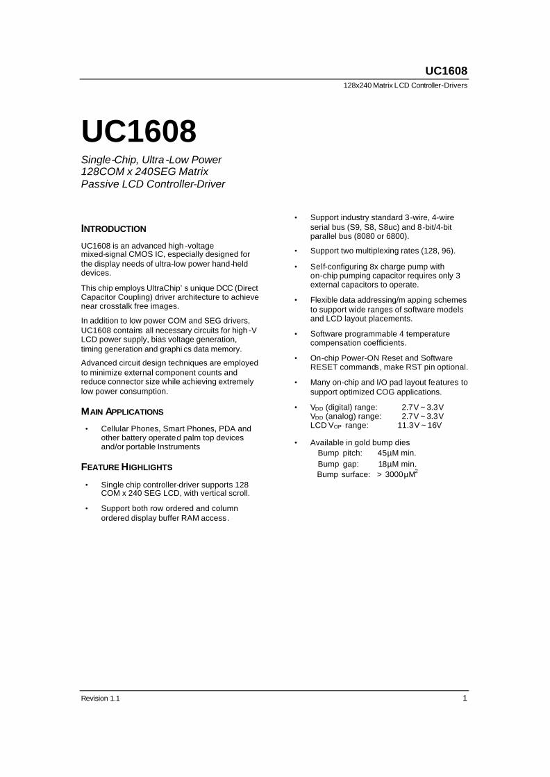
UC1608 Single-Chip, Ultra -Low Power 128COM x 240SEG Matrix Passive LCD Controller-Driver
INTRODUCTION
UC1608 is an advanced high -voltage mixed-signal CMOS IC, especially designed for the display needs of ultra-low power hand-held devices.
This chip employs UltraChip’s unique DCC (Direct Capacitor Coupling) driver architecture to achieve near crosstalk free images.
In addition to low power COM and SEG drivers, UC1608 contains all necessary circuits for high -V LCD power supply, bias voltage generation, timing generation and graphi cs data memory.
Advanced circuit design techniques are employed to minimize external component counts and reduce connector size while achieving extremely low power consumption.
MAIN APPLICATIONS
• Cellular Phones, Smart Phones, PDA and other battery operated palm top devices and/or portable Instruments
FEATURE HIGHLIGHTS
• Single chip controller-driver supports 128 COM x 240 SEG LCD, with vertical scroll.
• Support both row ordered and column ordered display buffer RAM access.
• Support industry standard 3-wire, 4-wire serial bus (S9, S8, S8uc) and 8-bit/4-bit parallel bus (8080 or 6800).
• Support two multiplexing rates (128, 96).
• Self-configuring 8x charge pump with on-chip pumping capacitor requires only 3 external capacitors to operate.
• Flexible data addressing/m apping schemes to support wide ranges of software models and LCD layout placements.
• Software programmable 4 temperature compensation coefficients.
• On-chip Power-ON Reset and Software RESET commands, make RST pin optional.
• Many on-chip and I/O pad layout features to support optimized COG applications.
• VDD (digital) range: 2.7V ~ 3.3V VDD (analog) range: 2.7V ~ 3.3V LCD VOP range: 11.3V ~ 16V
• Available in gold bump dies Bump pitch: 45µM min. Bump gap: 18µM min. Bump surface: > 3000µM2
ULTRACHIP
High-Voltage Mixed-Signal IC ©1999~2004
2 MP Specifications
ORDERING INFORMATION
Product ID Description
UC1608xGBE Gold bumped die.
UC1608xFBE COF packaging.
General Notes
APPLICATION INFORMATION
For improved readability, the specification contains many application data points. When application information is given, it is advisory and does not form part of the specification for the device.
BARE DIE DISCLAIMER
All die are tested and are guaranteed to comply with all data sheet limits up to the point of wafer sawing for a period of ninety (90) days from the date of UltraChip’s delivery. There is no post waffle saw/pack testing performed on individual die. Although the latest modern processes are utilized for wafer sawing and die pick-&-place into waffle pack carriers, UltraChip has no control of third party procedures in the handling, packing or assembly of the die. Accordingly, it is the responsibility of the customer to test and quality their application in which the die is to be us ed. UltraChip assumes no liability for device functionality or performance of the die or systems after handling, packing or assembly of the die.
LIFE SUPPORT APPLICATIONS
These devices are not designed for use in life support appliances, or systems where malfunction of these products can reasonably be expected to result in personal injuries. Customer using or selling these products for use in such applications do so at their own risk.
CONTENT DISCLAIMER
UltraChip believes the information contained in this document to be accurate and reliable. However, it is subject to change without notice. No responsibility is assumed by UltraChip for its use, nor for infringement of patents or other rights of third parties. No part of this publication may be reproduced, or transmitted in any form or by any means without the prior consent of UltraChip Inc. UltraChip's terms and conditions of sale apply at all times.
CONTACT INFORMATION
UltraChip Inc. (Headquarter) 2F, No. 70, Chowtze Street, Nei Hu District, Taipei 114, Taiwan, R. O. C.
Tel: +886 (2) 8797-8947 Fax: +886 (2) 8797-8910 Sales e-mail: [email protected] Web site: http://www.ultrachip.com
UC1608 128x240 Matrix LCD Controller-Drivers
Revision 1.1 3
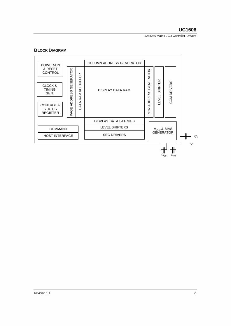
BLOCK DIAGRAM
CO
M D
RIV
ER
S
SEG DRIVERS
POWER-ON & RESET CONTROL
RO
W A
DD
RE
SS
GE
NE
RA
TO
R
CLOCK & TIMING GEN.
HOST INTERFACE
CONTROL & STATUS
REGISTER
COMMAND DECODER
COLUMN ADDRESS GENERATOR
DISPLAY DATA RAM
DISPLAY DATA LATCHES
LEVEL SHIFTERS
LEV
EL
SH
IFT
ER
VLCD & BIAS
GENERATOR
PA
GE
AD
DR
ES
S G
EN
ER
AT
OR
DA
TA
RA
M I/
O B
UF
FE
R
CL
CB1 CB0
ULTRACHIP
High-Voltage Mixed-Signal IC ©1999~2004
4 MP Specifications
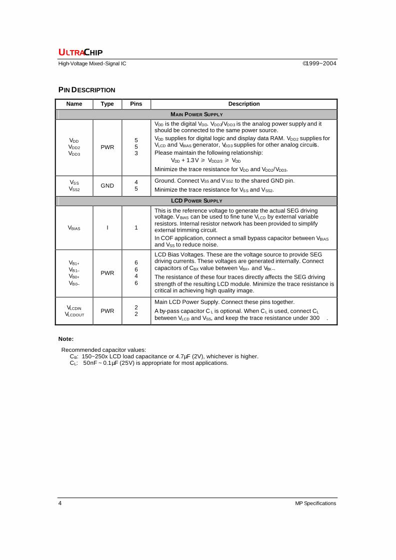
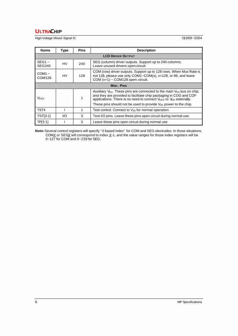
PIN DESCRIPTION
Name Type Pins Description
MAIN POWER SUPPLY
VDD
VDD2
VDD3 PWR
5 5 3
VDD is the digital VDD. VDD2/VDD3 is the analog power supply and it should be connected to the same power source. VDD supplies for digital logic and display data RAM. VDD2 supplies for VLCD and VBIAS generator, VDD3 supplies for other analog circuits. Please maintain the following relationship:
VDD + 1.3V / VDD2/3 / VDD
Minimize the trace resistance for VDD and VDD2/VDD3.
VSS
VSS2 GND 4 5
Ground. Connect VSS and VSS2 to the shared GND pin.
Minimize the trace resistance for VSS and VSS2.
LCD POWER SUPPLY
VBIAS I 1
This is the reference voltage to generate the actual SEG driving voltage. VBIAS can be used to fine tune VLCD by external variable resistors. Internal resistor network has been provided to simplify external trimming circuit. In COF application, connect a small bypass capacitor between VBIAS and VSS to reduce noise.
VB1+ VB1–
VB0+ VB0–
PWR
6 6 4 6
LCD Bias Voltages. These are the voltage source to provide SEG driving currents. These voltages are generated internally. Connect capacitors of CBX value between VBX+ and VBX–.
The resistance of these four traces directly affects the SEG driving strength of the resulting LCD module. Minimize the trace resistance is critical in achieving high quality image.
VLCDIN
VLCDOUT PWR 2 2
Main LCD Power Supply. Connect these pins together.
A by-pass capacitor C L is optional. When CL is used, connect CL between VLCD and VSS, and keep the trace resistance under 300 Ω.
Note:
Recommended capacitor values: CB: 150~250x LCD load capacitance or 4.7µF (2V), whichever is higher. CL: 50nF ~ 0.1µF (25V) is appropriate for most applications.
UC1608 128x240 Matrix LCD Controller-Drivers
Revision 1.1 5
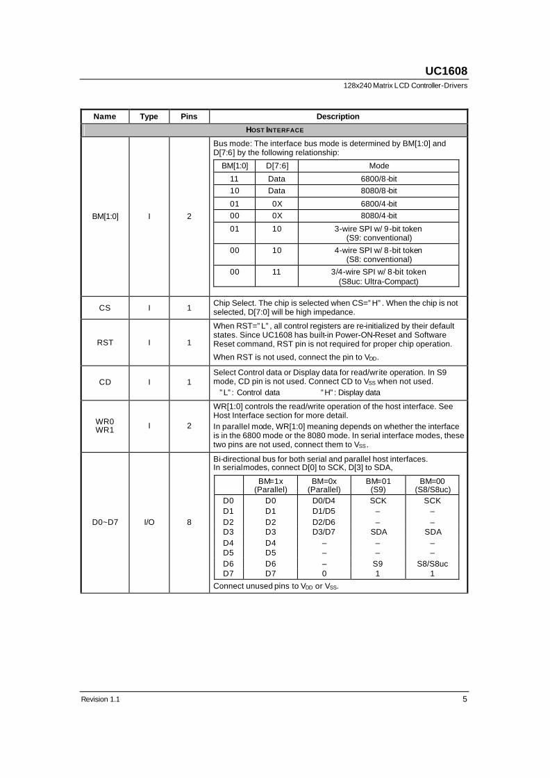
Name Type Pins Description
HOST INTERFACE
BM[1:0] I 2
Bus mode: The interface bus mode is determined by BM[1:0] and D[7:6] by the following relationship:
BM[1:0] D[7:6] Mode
11 Data 6800/8-bit 10 Data 8080/8-bit
01 0X 6800/4-bit 00 0X 8080/4-bit
01 10 3-wire SPI w/ 9-bit token (S9: conventional)
00 10 4-wire SPI w/ 8-bit token (S8: conventional)
00 11 3/4-wire SPI w/ 8-bit token (S8uc: Ultra-Compact)
CS I 1 Chip Select. The chip is selected when CS=”H”. When the chip is not selected, D[7:0] will be high impedance.
RST I 1
When RST=”L”, all control registers are re-initialized by their default states. Since UC1608 has built-in Power-ON-Reset and Software Reset command, RST pin is not required for proper chip operation.
When RST is not used, connect the pin to VDD.
CD I 1 Select Control data or Display data for read/write operation. In S9 mode, CD pin is not used. Connect CD to VSS when not used. ”L”: Control data ”H”: Display data
WR0 WR1 I 2
WR[1:0] controls the read/write operation of the host interface. See Host Interface section for more detail. In parallel mode, WR[1:0] meaning depends on whether the interface is in the 6800 mode or the 8080 mode. In serial interface modes, these two pins are not used, connect them to VSS.
D0~D7 I/O 8
Bi-directional bus for both serial and parallel host interfaces. In serial modes, connect D[0] to SCK, D[3] to SDA,
BM=1x (Parallel)
BM=0x (Parallel)
BM=01 (S9)
BM=00 (S8/S8uc)
D0 D0 D0/D4 SCK SCK D1 D1 D1/D5 – – D2 D2 D2/D6 – – D3 D3 D3/D7 SDA SDA D4 D4 – – – D5 D5 – – – D6 D6 – S9 S8/S8uc D7 D7 0 1 1
Connect unused pins to VDD or VSS.
ULTRACHIP
High-Voltage Mixed-Signal IC ©1999~2004
6 MP Specifications
Name Type Pins Description
LCD DRIVER OUTPUT
SEG1 ~ SEG240 HV 240 SEG (column) driver outputs. Support up to 240 columns.
Leave unused drivers open-circuit.
COM1 ~ COM128 HV 128
COM (row) driver outputs. Support up to 128 rows. When Mux Rate is not 128, please use only COM1~COM(x), x=128, or 96, and leave COM (x+1) ~ COM128 open-circuit.
MISC . PINS
VDDX 1
Auxiliary VDD. These pins are connected to the main VDD bus on chip, and they are provided to facilitate chip packaging in COG and COF applications. There is no need to connect VDDX to VDD externally. These pins should not be used to provide VDD power to the chip.
TST4 I 1 Test control. Connect to VSS for normal operation.
TST[3:1] I/O 3 Test I/O pins. Leave these pins open circuit during normal use.
TP[3:1] I 3 Leave these pins open circuit during normal use. Note: Several control registers will specify “0 based index” for COM and SEG electrodes. In those situations,
COMX or SEGX will correspond to index X-1, and the value ranges for those index registers will be 0~127 for COM and 0~239 for SEG.
UC1608 128x240 Matrix LCD Controller-Drivers
Revision 1.1 7
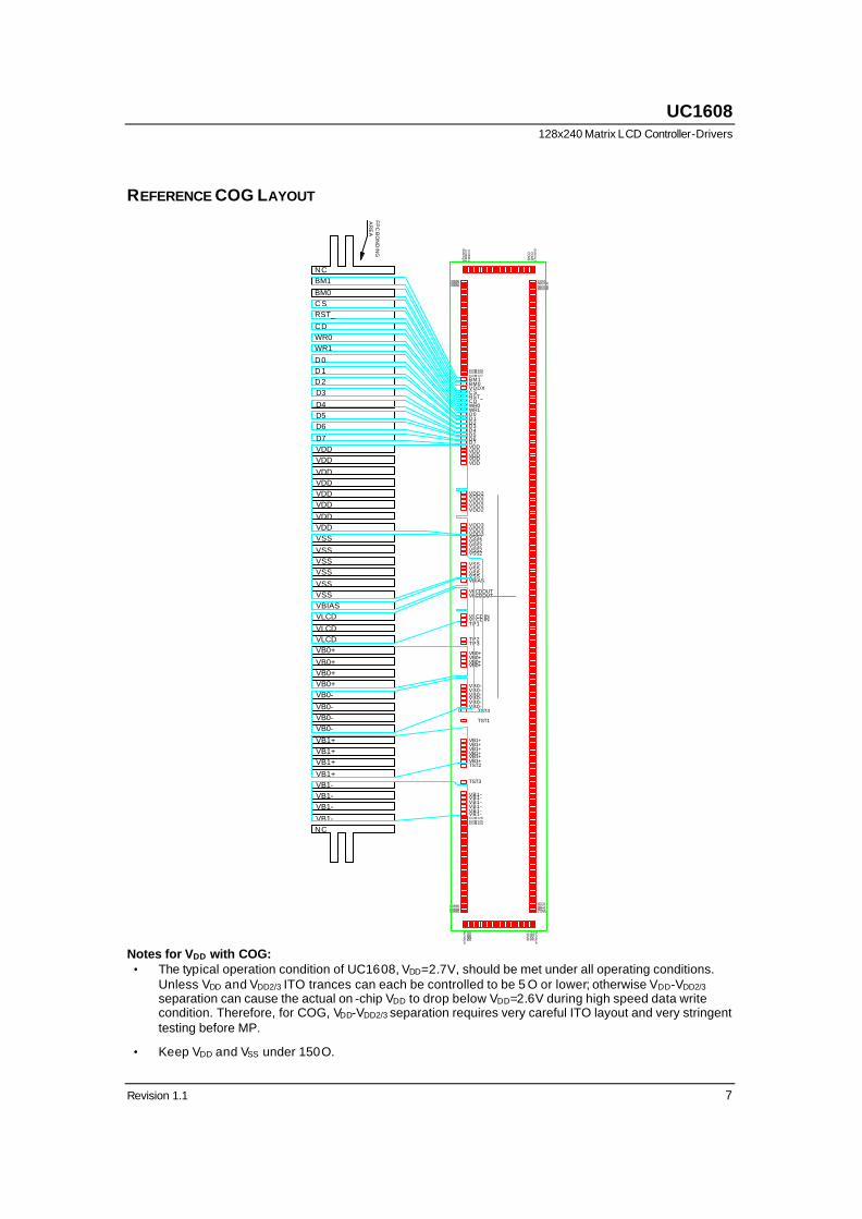
REFERENCE COG LAYOUT
FP
C B
ON
DIN
GA
RE
A
dumm
y1C
OM
3C
OM
5
CO
M5
1C
OM
53
dumm
y2
COM55COM57COM59
COM123COM125COM127BM1BM0VDDXC SRST_CDWR0WR1D0D1D2D3D4D5D6D7VDDVDDVDDVDDVDD
VDD2VDD2VDD2VDD2VDD2
VDD3VDD3VDD3VSS2VSS2VSS2VSS2VSS2
VSSVSSVSSVSSVBIAS
VLCDOUTVLCDOUT
VLCDINVLCDINTP1
TP2TP3
VB0+VB0+VB0+VB0+
VB0-VB0-VB0-VB0-VB0-VB0-
TST4
TST1
VB1+VB1+VB1+VB1+VB1+VB1+TST2
TST3
VB1-VB1-VB1-VB1-VB1-VB1-COM128COM126COM124
COM60COM58COM56
dumm
y3C
OM
54C
OM
52
CO
M8
CO
M6
CO
M4
dumm
y4
COM2SEG1SEG2SEG3
SEG238SEG239SEG240COM1
WR1
C SRST_
CDWR0
NCBM1
BM0
D6
D7
D5
VDD
D1D0
D2D3
D4
NC
VDD
VDDVDDVDDVDD
VDDVDDVSS
VSSVSSVSS
VBIASVLCD
VLCDVLCDVB0+
VB0+VB0+VB0+VB0-
VB0-VB0-VB0-
VB1+VB1+VB1+
VB1+VB1-VB1-VB1-
VB1-
VSSVSS
Notes for VDD with COG:
• The typical operation condition of UC1608, VDD=2.7V, should be met under all operating conditions. Unless VDD and VDD2/3 ITO trances can each be controlled to be 5 O or lower; otherwise VDD-VDD2/3
separation can cause the actual on -chip VDD to drop below VDD=2.6V during high speed data write condition. Therefore, for COG, VDD-VDD2/3 separation requires very careful ITO layout and very stringent testing before MP.
• Keep VDD and VSS under 150O.
ULTRACHIP
High-Voltage Mixed-Signal IC ©1999~2004
8 MP Specifications
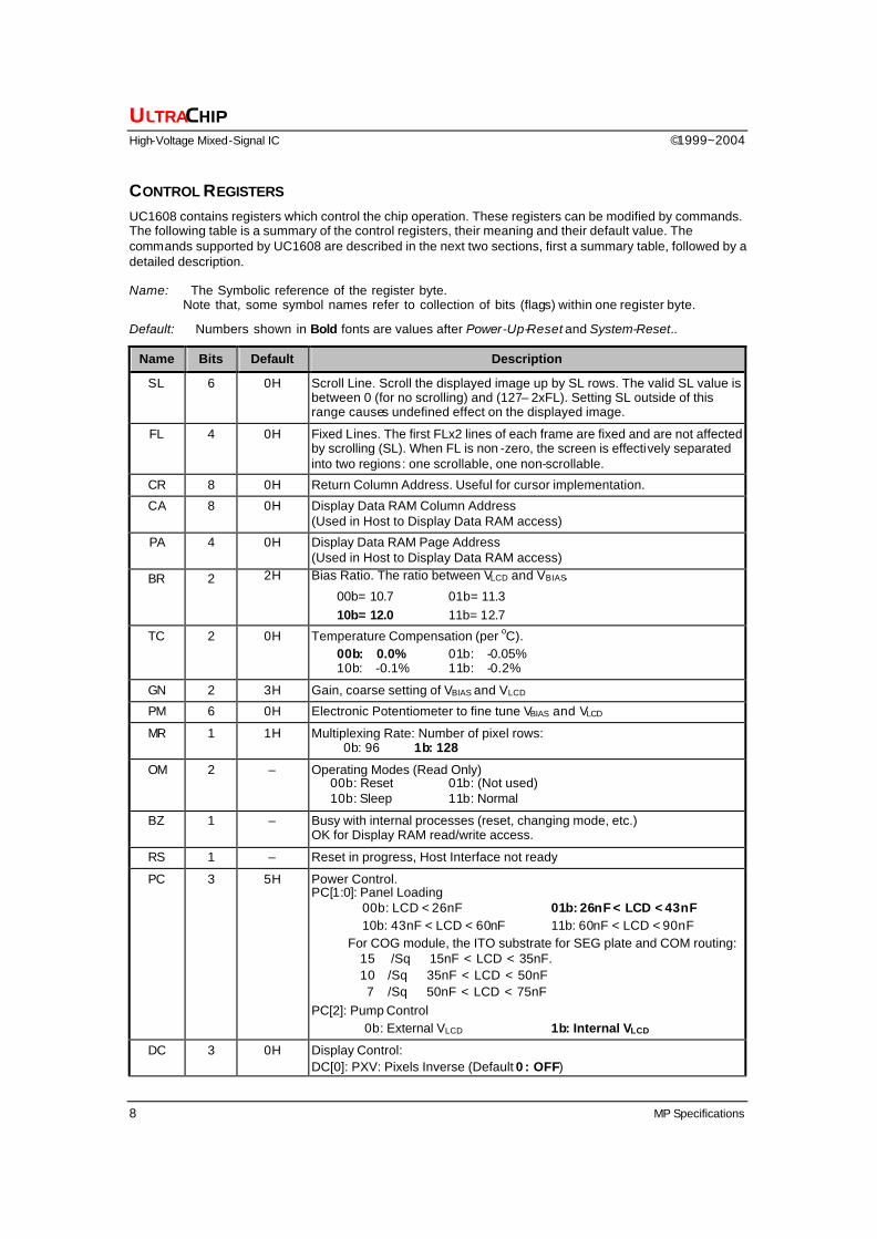
CONTROL REGISTERS UC1608 contains registers which control the chip operation. These registers can be modified by commands. The following table is a summary of the control registers, their meaning and their default value. The commands supported by UC1608 are described in the next two sections, first a summary table, followed by a detailed description. Name: The Symbolic reference of the register byte. Note that, some symbol names refer to collection of bits (flags) within one register byte.
Default: Numbers shown in Bold fonts are values after Power-Up-Reset and System-Reset..
Name Bits Default Description
SL 6 0H Scroll Line. Scroll the displayed image up by SL rows. The valid SL value is between 0 (for no scrolling) and (127– 2xFL). Setting SL outside of this range causes undefined effect on the displayed image.
FL 4 0H Fixed Lines. The first FLx2 lines of each frame are fixed and are not affected by scrolling (SL). When FL is non -zero, the screen is effectively separated into two regions: one scrollable, one non-scrollable.
CR 8 0H Return Column Address. Useful for cursor implementation.
CA 8 0H Display Data RAM Column Address (Used in Host to Display Data RAM access)
PA 4 0H Display Data RAM Page Address (Used in Host to Display Data RAM access)
BR 2 2H Bias Ratio. The ratio between VLCD and VBIAS.
00b= 10.7 01b= 11.3 10b= 12.0 11b= 12.7
TC 2 0H Temperature Compensation (per oC). 00b: 0.0% 01b: -0.05% 10b: -0.1% 11b: -0.2%
GN 2 3H Gain, coarse setting of VBIAS and VLCD
PM 6 0H Electronic Potentiometer to fine tune VBIAS and VLCD
MR 1 1H Multiplexing Rate: Number of pixel rows: 0b: 96 1b: 128
OM 2 – Operating Modes (Read Only) 00b: Reset 01b: (Not used) 10b: Sleep 11b: Normal
BZ 1 – Busy with internal processes (reset, changing mode, etc.) OK for Display RAM read/write access.
RS 1 – Reset in progress, Host Interface not ready
PC 3 5H Power Control. PC[1:0]: Panel Loading 00b: LCD < 26nF 01b: 26nF < LCD < 43nF
10b: 43nF < LCD < 60nF 11b: 60nF < LCD < 90nF For COG module, the ITO substrate for SEG plate and COM routing:
15 Ω/Sq 15nF < LCD < 35nF. 10Ω/Sq 35nF < LCD < 50nF 7Ω/Sq 50nF < LCD < 75nF
PC[2]: Pump Control 0b: External VLCD 1b: Internal VLCD
DC 3 0H Display Control: DC[0]: PXV: Pixels Inverse (Default 0 : OFF)
UC1608 128x240 Matrix LCD Controller-Drivers
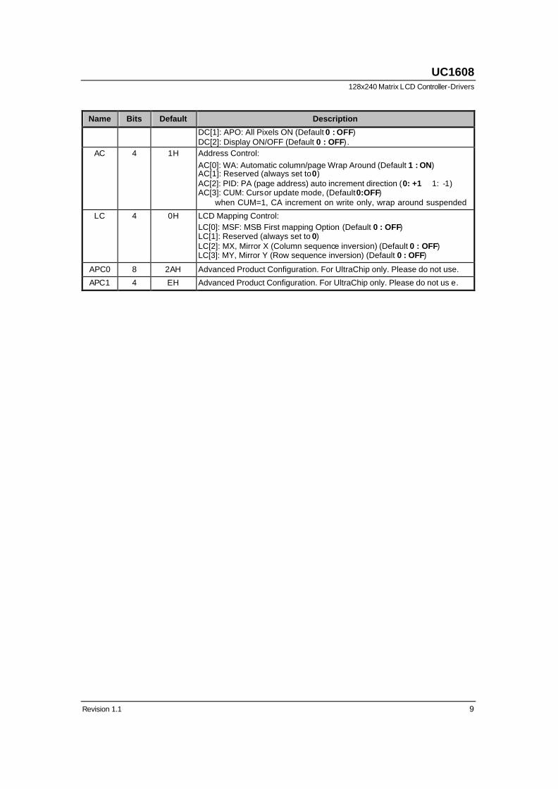
Revision 1.1 9
Name Bits Default Description
DC[1]: APO: All Pixels ON (Default 0 : OFF) DC[2]: Display ON/OFF (Default 0 : OFF).
AC 4 1H Address Control: AC[0]: WA: Automatic column/page Wrap Around (Default 1 : ON) AC[1]: Reserved (always set to 0) AC[2]: PID: PA (page address) auto increment direction (0: +1 1: -1) AC[3]: CUM: Cursor update mode, (Default 0:OFF) when CUM=1, CA increment on write only, wrap around suspended
LC 4 0H LCD Mapping Control: LC[0]: MSF: MSB First mapping Option (Default 0 : OFF) LC[1]: Reserved (always set to 0) LC[2]: MX, Mirror X (Column sequence inversion) (Default 0 : OFF) LC[3]: MY, Mirror Y (Row sequence inversion) (Default 0 : OFF)
APC0 8 2AH Advanced Product Configuration. For UltraChip only. Please do not use.
APC1 4 EH Advanced Product Configuration. For UltraChip only. Please do not us e.
ULTRACHIP
High-Voltage Mixed-Signal IC ©1999~2004
10 MP Specifications
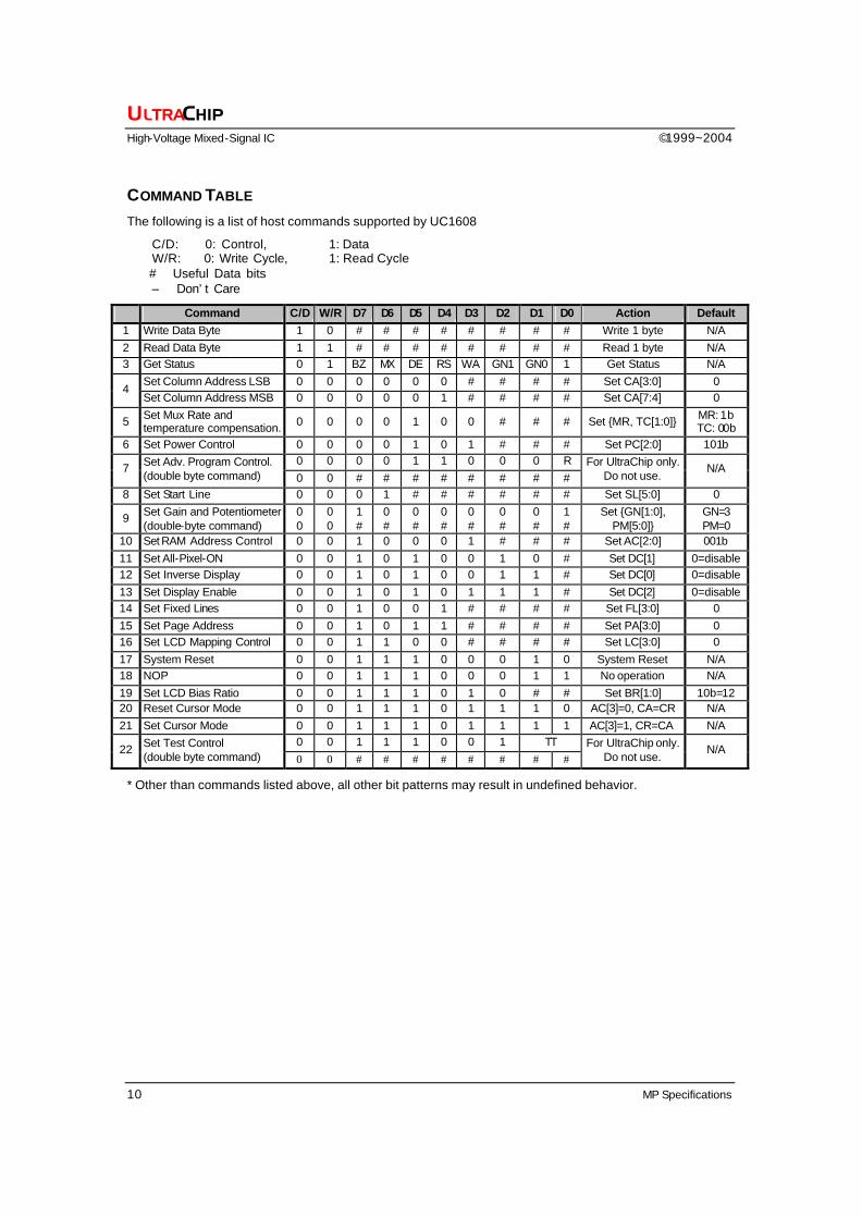
COMMAND TABLE The following is a list of host commands supported by UC1608
C/D: 0: Control, 1: Data W/R: 0: Write Cycle, 1: Read Cycle # Useful Data bits – Don’t Care
Command C/D W/R D7 D6 D5 D4 D3 D2 D1 D0 Action Default 1 Write Data Byte 1 0 # # # # # # # # Write 1 byte N/A 2 Read Data Byte 1 1 # # # # # # # # Read 1 byte N/A 3 Get Status 0 1 BZ MX DE RS WA GN1 GN0 1 Get Status N/A
Set Column Address LSB 0 0 0 0 0 0 # # # # Set CA[3:0] 0 4
Set Column Address MSB 0 0 0 0 0 1 # # # # Set CA[7:4] 0
5 Set Mux Rate and temperature compensation. 0 0 0 0 1 0 0 # # # Set {MR, TC[1:0]} MR: 1b
TC: 00b 6 Set Power Control 0 0 0 0 1 0 1 # # # Set PC[2:0] 101b
0 0 0 0 1 1 0 0 0 R 7 Set Adv. Program Control.
(double byte command) 0 0 # # # # # # # # For UltraChip only.
Do not use. N/A
8 Set Start Line 0 0 0 1 # # # # # # Set SL[5:0] 0
9 Set Gain and Potentiometer (double-byte command)
0 0
0 0
1 #
0 #
0 #
0 #
0 #
0 #
0 #
1 #
Set {GN[1:0], PM[5:0]}
GN=3 PM=0
10 Set RAM Address Control 0 0 1 0 0 0 1 # # # Set AC[2:0] 001b 11 Set All-Pixel-ON 0 0 1 0 1 0 0 1 0 # Set DC[1] 0=disable 12 Set Inverse Display 0 0 1 0 1 0 0 1 1 # Set DC[0] 0=disable 13 Set Display Enable 0 0 1 0 1 0 1 1 1 # Set DC[2] 0=disable 14 Set Fixed Lines 0 0 1 0 0 1 # # # # Set FL[3:0] 0 15 Set Page Address 0 0 1 0 1 1 # # # # Set PA[3:0] 0 16 Set LCD Mapping Control 0 0 1 1 0 0 # # # # Set LC[3:0] 0 17 System Reset 0 0 1 1 1 0 0 0 1 0 System Reset N/A 18 NOP 0 0 1 1 1 0 0 0 1 1 No operation N/A 19 Set LCD Bias Ratio 0 0 1 1 1 0 1 0 # # Set BR[1:0] 10b=12 20 Reset Cursor Mode 0 0 1 1 1 0 1 1 1 0 AC[3]=0, CA=CR N/A 21 Set Cursor Mode 0 0 1 1 1 0 1 1 1 1 AC[3]=1, CR=CA N/A
0 0 1 1 1 0 0 1 TT 22 Set Test Control
(double byte command) 0 0 # # # # # # # # For UltraChip only.
Do not use. N/A
* Other than commands listed above, all other bit patterns may result in undefined behavior.
UC1608 128x240 Matrix LCD Controller-Drivers
Revision 1.1 11
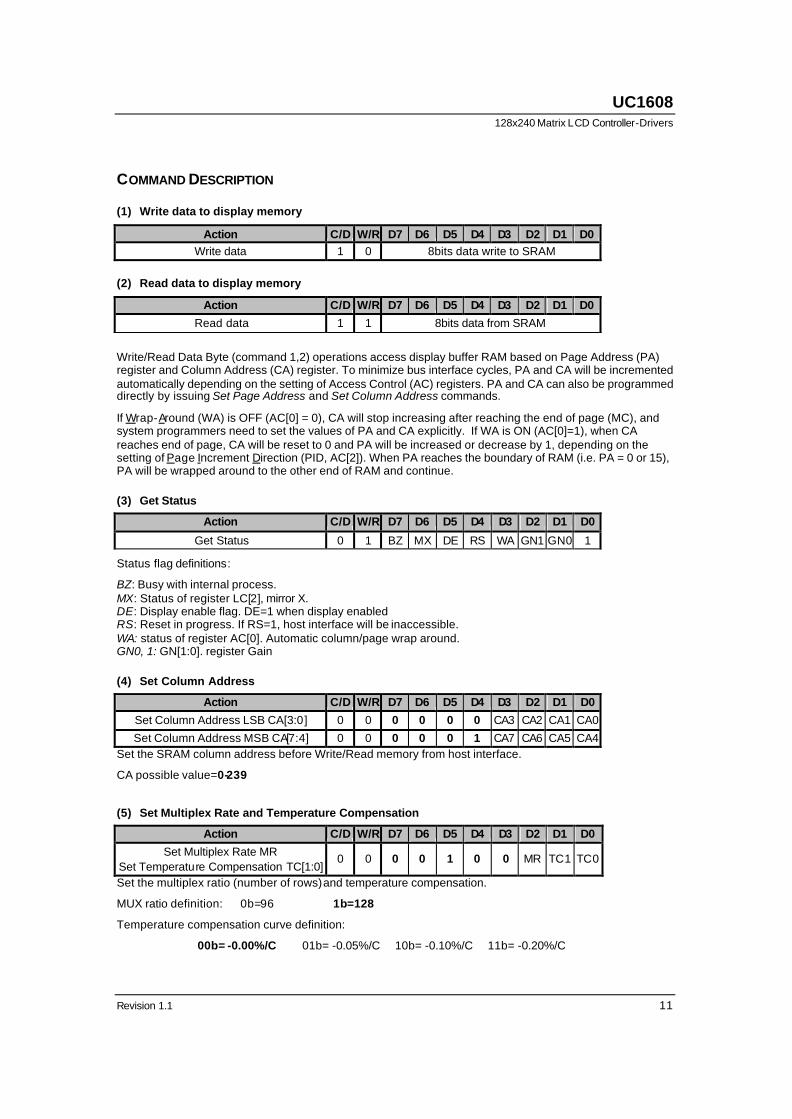
COMMAND DESCRIPTION
(1) Write data to display memory
Action C/D W/R D7 D6 D5 D4 D3 D2 D1 D0 Write data 1 0 8bits data write to SRAM
(2) Read data to display memory
Action C/D W/R D7 D6 D5 D4 D3 D2 D1 D0
Read data 1 1 8bits data from SRAM
Write/Read Data Byte (command 1,2) operations access display buffer RAM based on Page Address (PA) register and Column Address (CA) register. To minimize bus interface cycles, PA and CA will be incremented automatically depending on the setting of Access Control (AC) registers. PA and CA can also be programmed directly by issuing Set Page Address and Set Column Address commands.
If Wrap-Around (WA) is OFF (AC[0] = 0), CA will stop increasing after reaching the end of page (MC), and system programmers need to set the values of PA and CA explicitly. If WA is ON (AC[0]=1), when CA reaches end of page, CA will be reset to 0 and PA will be increased or decrease by 1, depending on the setting of Page Increment Direction (PID, AC[2]). When PA reaches the boundary of RAM (i.e. PA = 0 or 15), PA will be wrapped around to the other end of RAM and continue.
(3) Get Status
Action C/D W/R D7 D6 D5 D4 D3 D2 D1 D0
Get Status 0 1 BZ MX DE RS WA GN1 GN0 1
Status flag definitions:
BZ: Busy with internal process. MX: Status of register LC[2], mirror X. DE: Display enable flag. DE=1 when display enabled RS: Reset in progress. If RS=1, host interface will be inaccessible. WA: status of register AC[0]. Automatic column/page wrap around. GN0, 1: GN[1:0]. register Gain
(4) Set Column Address
Action C/D W/R D7 D6 D5 D4 D3 D2 D1 D0
Set Column Address LSB CA[3:0] 0 0 0 0 0 0 CA3 CA2 CA1 CA0
Set Column Address MSB CA[7:4] 0 0 0 0 0 1 CA7 CA6 CA5 CA4 Set the SRAM column address before Write/Read memory from host interface.
CA possible value=0-239
(5) Set Multiplex Rate and Temperature Compensation
Action C/D W/R D7 D6 D5 D4 D3 D2 D1 D0
Set Multiplex Rate MR Set Temperature Compensation TC[1:0]
0 0 0 0 1 0 0 MR TC1 TC0
Set the multiplex ratio (number of rows) and temperature compensation.
MUX ratio definition: 0b=96 1b=128
Temperature compensation curve definition:
00b= -0.00%/C 01b= -0.05%/C 10b= -0.10%/C 11b= -0.20%/C
ULTRACHIP
High-Voltage Mixed-Signal IC ©1999~2004
12 MP Specifications
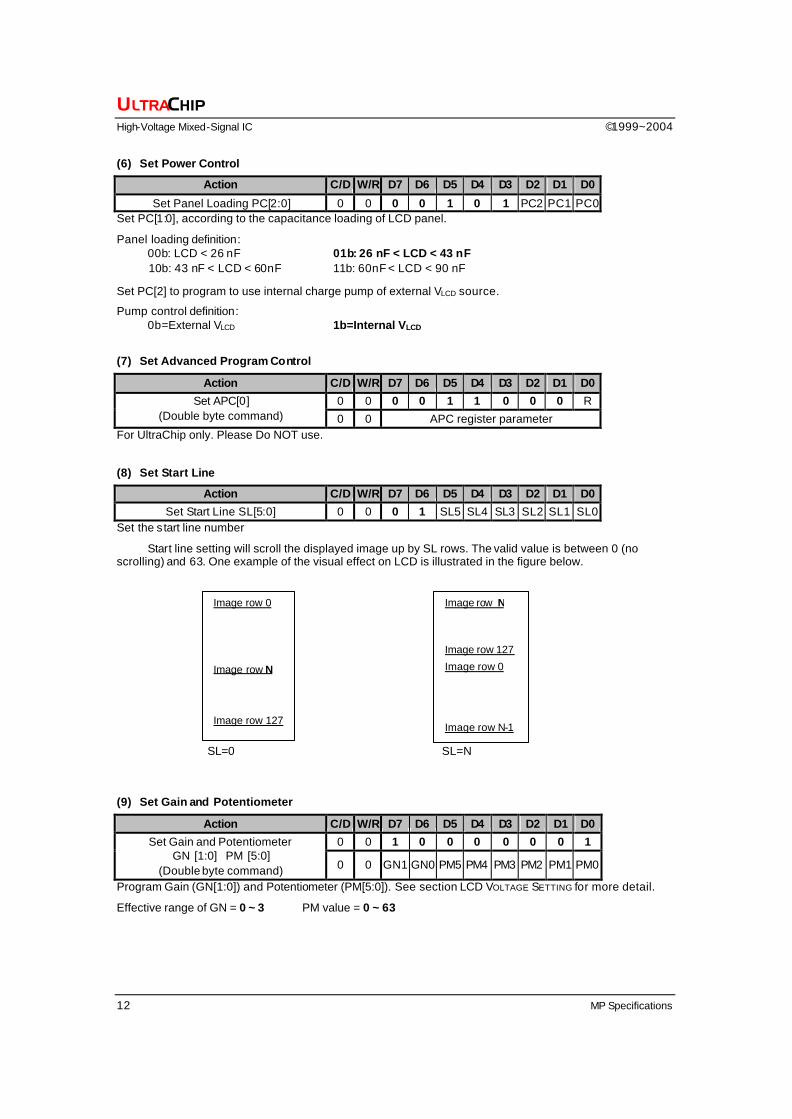
(6) Set Power Control
Action C/D W/R D7 D6 D5 D4 D3 D2 D1 D0
Set Panel Loading PC[2:0] 0 0 0 0 1 0 1 PC2 PC1 PC0 Set PC[1:0], according to the capacitance loading of LCD panel.
Panel loading definition: 00b: LCD < 26 nF 01b: 26 nF < LCD < 43 nF
10b: 43 nF < LCD < 60nF 11b: 60nF < LCD < 90 nF Set PC[2] to program to use internal charge pump of external VLCD source.
Pump control definition: 0b=External VLCD 1b=Internal VLCD
(7) Set Advanced Program Control
Action C/D W/R D7 D6 D5 D4 D3 D2 D1 D0
0 0 0 0 1 1 0 0 0 R Set APC[0] (Double byte command) 0 0 APC register parameter
For UltraChip only. Please Do NOT use.
(8) Set Start Line
Action C/D W/R D7 D6 D5 D4 D3 D2 D1 D0
Set Start Line SL[5:0] 0 0 0 1 SL5 SL4 SL3 SL2 SL1 SL0 Set the start line number
Start line setting will scroll the displayed image up by SL rows. The valid value is between 0 (no scrolling) and 63. One example of the visual effect on LCD is illustrated in the figure below.
SL=0 SL=N
(9) Set Gain and Potentiometer
Action C/D W/R D7 D6 D5 D4 D3 D2 D1 D0
0 0 1 0 0 0 0 0 0 1 Set Gain and Potentiometer GN [1:0] PM [5:0]
(Double byte command) 0 0 GN1 GN0 PM5 PM4 PM3 PM2 PM1 PM0
Program Gain (GN[1:0]) and Potentiometer (PM[5:0]). See section LCD VOLTAGE SETTING for more detail.
Effective range of GN = 0 ~ 3 PM value = 0 ~ 63
Image row 0
Image row N
Image row 127
Image row N Image row 127
Image row 0 Image row N-1
UC1608 128x240 Matrix LCD Controller-Drivers
Revision 1.1 13
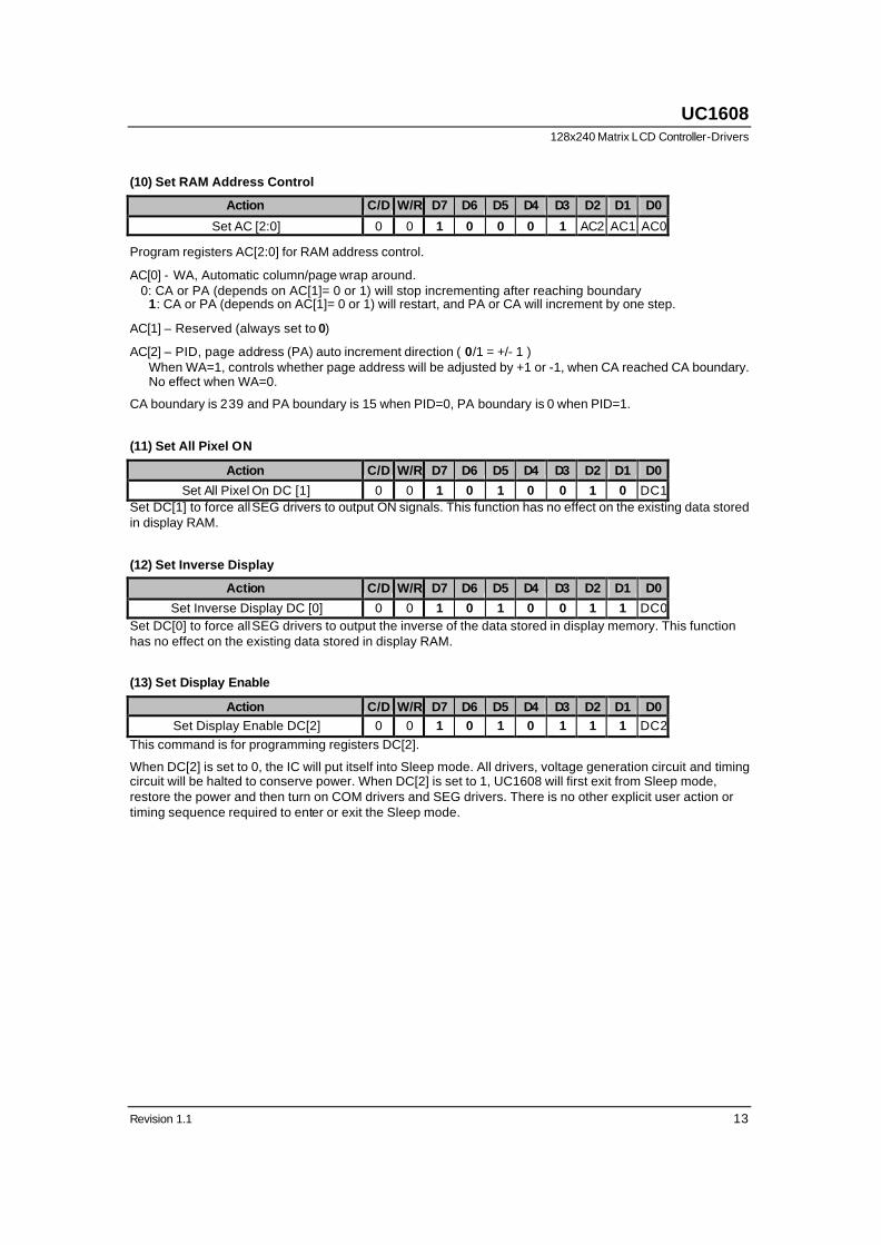
(10) Set RAM Address Control
Action C/D W/R D7 D6 D5 D4 D3 D2 D1 D0
Set AC [2:0] 0 0 1 0 0 0 1 AC2 AC1 AC0
Program registers AC[2:0] for RAM address control.
AC[0] - WA, Automatic column/page wrap around. 0: CA or PA (depends on AC[1]= 0 or 1) will stop incrementing after reaching boundary 1: CA or PA (depends on AC[1]= 0 or 1) will restart, and PA or CA will increment by one step.
AC[1] – Reserved (always set to 0)
AC[2] – PID, page address (PA) auto increment direction ( 0/1 = +/- 1 ) When WA=1, controls whether page address will be adjusted by +1 or -1, when CA reached CA boundary. No effect when WA=0.
CA boundary is 239 and PA boundary is 15 when PID=0, PA boundary is 0 when PID=1.
(11) Set All Pixel ON
Action C/D W/R D7 D6 D5 D4 D3 D2 D1 D0
Set All Pixel On DC [1] 0 0 1 0 1 0 0 1 0 DC1Set DC[1] to force all SEG drivers to output ON signals. This function has no effect on the existing data stored in display RAM.
(12) Set Inverse Display
Action C/D W/R D7 D6 D5 D4 D3 D2 D1 D0
Set Inverse Display DC [0] 0 0 1 0 1 0 0 1 1 DC0Set DC[0] to force all SEG drivers to output the inverse of the data stored in display memory. This function has no effect on the existing data stored in display RAM.
(13) Set Display Enable
Action C/D W/R D7 D6 D5 D4 D3 D2 D1 D0 Set Display Enable DC[2] 0 0 1 0 1 0 1 1 1 DC2
This command is for programming registers DC[2].
When DC[2] is set to 0, the IC will put itself into Sleep mode. All drivers, voltage generation circuit and timing circuit will be halted to conserve power. When DC[2] is set to 1, UC1608 will first exit from Sleep mode, restore the power and then turn on COM drivers and SEG drivers. There is no other explicit user action or timing sequence required to enter or exit the Sleep mode.
ULTRACHIP
High-Voltage Mixed-Signal IC ©1999~2004
14 MP Specifications
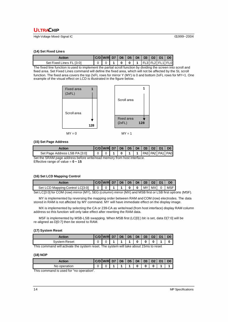
(14) Set Fixed Lines
Action C/D W/R D7 D6 D5 D4 D3 D2 D1 D0
Set Fixed Lines FL [3:0] 0 0 1 0 0 1 FL3 FL2 FL1 FL0 The fixed line function is used to implement the partial scroll function by dividing the screen into scroll and fixed area. Set Fixed Lines command will define the fixed area, which will not be affected by the SL scroll function. The fixed area covers the top 2xFL rows for mirror Y (MY) is 0 and bottom 2xFL rows for MY=1. One example of the visual effect on LCD is illustrated in the figure below.
MY = 0 MY = 1
(15) Set Page Address
Action C/D W/R D7 D6 D5 D4 D3 D2 D1 D0 Set Page Address LSB PA [3:0] 0 0 1 0 1 1 PA3 PA2 PA1 PA0
Set the SRAM page address before write/read memory from host interface. Effective range of value = 0 ~ 15
(16) Set LCD Mapping Control
Action C/D W/R D7 D6 D5 D4 D3 D2 D1 D0
Set LCD Mapping Control LC[3:0] 0 0 1 1 0 0 MY MX 0 MSF Set LC[3:0] for COM (row) mirror (MY), SEG (column) mirror (MX) and MSB first or LSB first options (MSF).
MY is implemented by reversing the mapping order between RAM and COM (row) electrodes. The data stored in RAM is not affected by MY command. MY will have immediate effect on the display image.
MX is implemented by selecting the CA or 239-CA as write/read (from host interface) display RAM column address so this function will only take effect after rewriting the RAM data.
MSF is implemented by MSB-LSB swapping. When MSB first (LC[0] ) bit is set, data D[7:0] will be re-aligned as D[0:7] then be stored to RAM.
(17) System Reset
Action C/D W/R D7 D6 D5 D4 D3 D2 D1 D0 System Reset 0 0 1 1 1 0 0 0 1 0
This command will activate the system reset. The system will take about 15ms to reset
(18) NOP
Action C/D W/R D7 D6 D5 D4 D3 D2 D1 D0 No operation 0 0 1 1 1 0 0 0 1 1
This command is used for “no operation”.
Fixed area (2xFL) 128
1 Scroll area
Fixed area 1 (2xFL)
Scroll area
128
UC1608 128x240 Matrix LCD Controller-Drivers
Revision 1.1 15
(19) Set LCD Bias Ratio
Action C/D W/R D7 D6 D5 D4 D3 D2 D1 D0
Set Bias Ratio BR [1:0] 0 0 1 1 1 0 1 0 BR1 BR0 Bias ratio definition:
00b= 10.7 01b=11.3 10b=12.0 11b=12.7
(20) Reset Cursor Mode
Action C/D W/R D7 D6 D5 D4 D3 D2 D1 D0 Return to Cursor. AC[3]=0, CA=CR 0 0 1 1 1 0 1 1 1 0
This command is used to reset cursor update mode function. See description below.
(21) Set Cursor Mode
Action C/D W/R D7 D6 D5 D4 D3 D2 D1 D0 Set AC[3]=1 CR=CA 0 0 1 1 1 0 1 1 1 1
Set Cursor Mode command is used to turn on cursor update mode function. AC[3] will be set to 1, register CR will be set to the value of register CA
When AC[3]=1, column address (CA) will only increment with write RAM operation but not on read RAM operation. The address CA wraps around will also be suspended no matter what WA setting is. The purpose of this combination of features is to support “Read-Modify-Write” for cursor implementation.
Reset Cursor Mode command will clear cursor update mode flag (AC[3]=0), CA will be restored to previous CA value which is stored in CR, and CA, PA increment will return to its normal condition.
(22) Set Test Control
Action C/D W/R D7 D6 D5 D4 D3 D2 D1 D0
0 0 1 1 1 0 0 1 TT Set TT (Double byte command) 0 0 Testing parameter
This command is used for UltraChip production testing. For UltraChip Only. Please do not use.
ULTRACHIP
High-Voltage Mixed-Signal IC ©1999~2004
16 MP Specifications
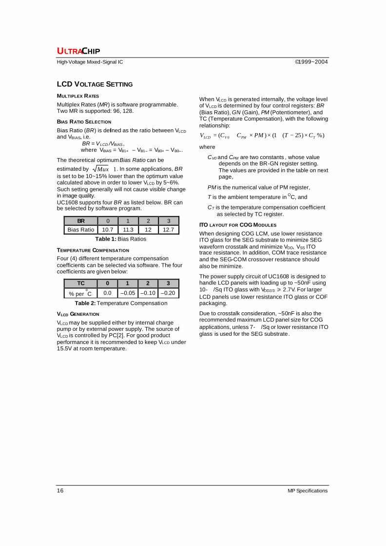
LCD VOLTAGE SETTING
MULTIPLEX RATES
Multiplex Rates (MR) is software programmable. Two MR is supported: 96, 128.
BIAS RATIO SELECTION
Bias Ratio (BR) is defined as the ratio between VLCD and VBIAS, i.e. BR = VLCD /VBIAS , where VBIAS = VB1+ – VB1– = VB0+ – VB0– .
The theoretical optimum Bias Ratio can be
estimated by 1+Mux . In some applications, BR is set to be 10~15% lower than the optimum value calculated above in order to lower VLCD by 5~6%. Such setting generally will not cause visible change in image quality. UC1608 supports four BR as listed below. BR can be selected by software program.
BR 0 1 2 3
Bias Ratio 10.7 11.3 12 12.7
Table 1: Bias Ratios
TEMPERATURE COMPENSATION Four (4) different temperature compensation coefficients can be selected via software. The four coefficients are given below:
TC 0 1 2 3
% per oC 0.0 –0.05 –0.10 –0.20
Table 2: Temperature Compensation
VLCD GENERATION
VLCD may be supplied either by internal charge pump or by external power supply. The source of VLCD is controlled by PC[2]. For good product performance it is recommended to keep VLCD under 15.5V at room temperature.
When VLCD is generated internally, the voltage level of VLCD is determined by four control registers: BR (Bias Ratio), GN (Gain), PM (Potentiometer), and TC (Temperature Compensation), with the following relationship:
%))25(1()( 0 TPMVLCD CTPMCCV ×−+××+=
where
CV0 and CPM are two constants , whose value depends on the BR-GN register setting. The values are provided in the table on next page,
PM is the numerical value of PM register,
T is the ambient temperature in OC, and
CT is the temperature compensation coefficient as selected by TC register.
ITO LAYOUT FOR COG MODULES
When designing COG LCM, use lower resistance ITO glass for the SEG substrate to minimize SEG waveform crosstalk and minimize VDD, VSS ITO trace resistance. In addition, COM trace resistance and the SEG-COM crossover resistance should also be minimize.
The power supply circuit of UC1608 is designed to handle LCD panels with loading up to ~50nF using 10-Ω/Sq ITO glass with VDD2/3 / 2.7V. For larger LCD panels use lower resistance ITO glass or COF packaging.
Due to crosstalk consideration, ~50nF is also the recommended maximum LCD panel size for COG applications, unless 7-Ω/Sq or lower resistance ITO glass is used for the SEG substrate.
UC1608 128x240 Matrix LCD Controller-Drivers
Revision 1.1 17
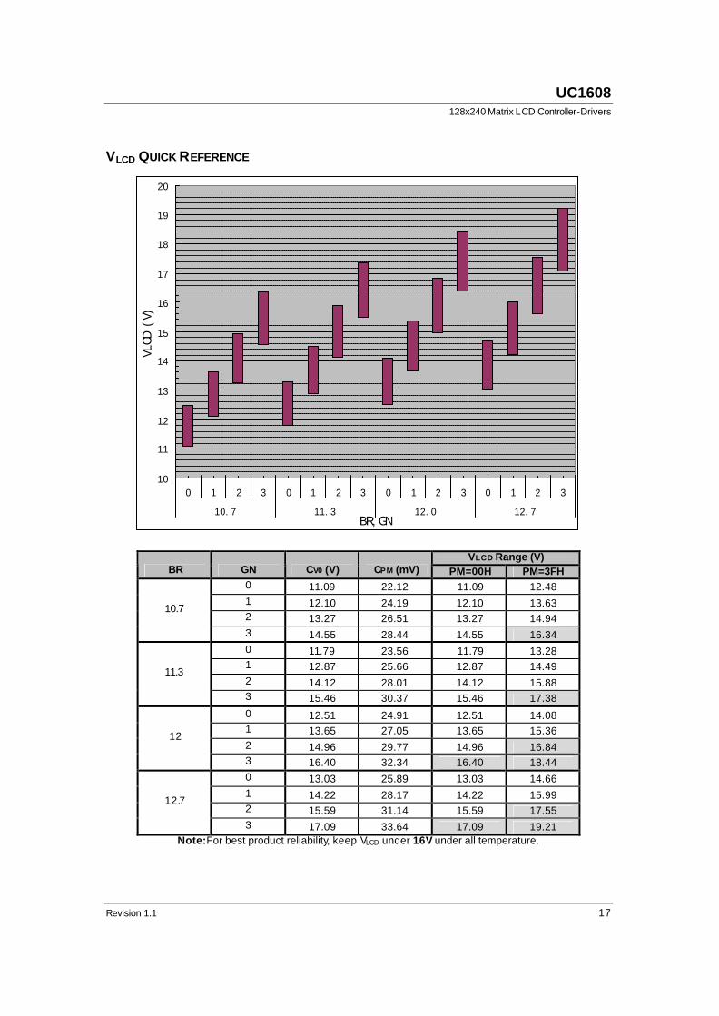
VLCD QUICK REFERENCE
10
11
12
13
14
15
16
17
18
19
20
0 1 2 3 0 1 2 3 0 1 2 3 0 1 2 3
10.7 11.3 12.0 12.7BR,GN
VLCD
(V)
VLCD Range (V) BR GN CV0 (V) CPM (mV) PM=00H PM=3FH
0 11.09 22.12 11.09 12.48 1 12.10 24.19 12.10 13.63 2 13.27 26.51 13.27 14.94
10.7
3 14.55 28.44 14.55 16.34 0 11.79 23.56 11.79 13.28 1 12.87 25.66 12.87 14.49 2 14.12 28.01 14.12 15.88
11.3
3 15.46 30.37 15.46 17.38 0 12.51 24.91 12.51 14.08 1 13.65 27.05 13.65 15.36 2 14.96 29.77 14.96 16.84
12
3 16.40 32.34 16.40 18.44 0 13.03 25.89 13.03 14.66 1 14.22 28.17 14.22 15.99 2 15.59 31.14 15.59 17.55
12.7
3 17.09 33.64 17.09 19.21 Note: For best product reliability, keep VLCD under 16V under all temperature.
ULTRACHIP
High-Voltage Mixed-Signal IC ©1999~2004
18 MP Specifications
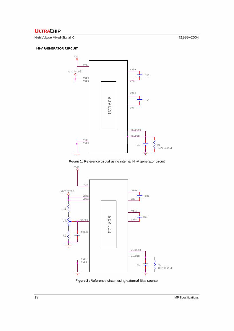
HI-V GENERATOR CIRCUIT
VLCDIN
VSS2
VDD3
VSS
VDD2
UC1608
VDDVB0+
CB0
VB0-
VB1-
CB1
VB1+
VDD
VLCDOUT
VDD2/VDD3
CL(OPTIONAL)RL
FIGURE 1: Reference circuit using internal Hi-V generator circuit
VB1-
VB0-
VDD
RL
VDD2
(OPTIONAL)
VDD2/VDD3
VSS
CL
VDD3
R2
VSS2
CBIAS
VDD
CB0
VBIAS
R1VB1+
CB1
VLCDIN
VR
UC1608
VLCDOUT
VB0+
Figure 2 : Reference circuit using external Bias source
UC1608 128x240 Matrix LCD Controller-Drivers
Revision 1.1 19
Note : • Recommended component values:
CB : 150 ~250x LCD load capacitance or 4.7µF (2V), whichever is higher. CL : 50nF ~ 0.1µF (25V) is appropriate for most applications. RL : 10MO. Acts as a draining circuit when the power is abnormally shut down. VR : 1M O. R1, R2: See instructions below. CBIAS : 10nF ~ 0.1µF is recommended.
• The above component values are for reference only. Please optimize the values for the individual requirements of each specific application.
• To ensure consistency of LCM contrast, VLCD fine tuning is highly recommended.
Since the value o f R1/R2 depends strongly on the GN, PM, BR settings, and vary slightly depends on the value of VDD2, each LCM design will need to be optimized individually.
The following is the recommended procedures for selecting R1, R2 and VR values.
Step 1: Adjust LCM for the best contrast with CBIAS, but without R1, R2, VR. Step 2: Measure VBIAS voltage Step 3: Select VR and R2 (recommend to start with VR=1M O, R2=200K) Step 4: Calculate R1 by: R1 = R2 x (VDD2/VBIAS -1) Step 5: Install R1, R2, VR. The “neutral position” of VR is at VBIAS /VDD2. Step 6: Test the fine tuning range by adjusting VR over the full range. Step 7: If adjustment range is too narrow, reduce R2, … and vise versa. Step 8: Repeat from Step 4.
• Step 2, Measure VBIAS, is a very critical step. Since the purpose of this circuit is to maximize the contrast consistency of mass production units, please fine tuning GN, PM, BR across at least 150~200 LCM units (without the VLCD adjustment circuit), before finalizing the values of PM, GN, BR. The average VBIAS should be measured after PM, GN and BR is selected and finalized.
• Please note that, the “Neutral position” of the VR (the position with minimum VLCD adjustment) is not the center, but located at VBIAS/VDD2. Relative to this “Neutral position”, the circuit produced by above procedure will have equal VLCD adjustment range of +N% ~ -N% for the average VLCD.
• Please avoid situations where the adjustment of the VR can push UC1608 out of its safe VLCD operation range (16V) at the low end of operating temperature range. If this happens, then it will be possible for the MP operators to damage the LCM by adjusting the VR.
• Since the value of VDD2 can affect the adjustment of the VR, please apply VDD2 that is intended to be used in the final application during the mass production VLCD tuning process.
• Due to its minor sensitivity to the value of VDD2, this VLCD tuning circuit may not be suitable for “standard product” where the actual VDD2 value can vary far over 5% from the design VDD2 value. For such applications, please use a Zener diode, such as Hitachi HZU3LL, to replace VDD2 as the power source for this VLCD fine tuning circuit.
ULTRACHIP
High-Voltage Mixed-Signal IC ©1999~2004
20 MP Specifications
LCD DISPLAY CONTROLS
CLOCK & TIMING GENERATOR
UC1608 contains a built-in system clock. All required components for the clock oscillator are built-in. No external parts are required.
DRIVER MODES
COM and SEG drivers can be in either Idle mode or Active mode, controlled by Display Enable flag (DC[2]). When COM drivers are in idle mode, their outputs are high-impedance (open circuit). When SEG drivers are in idle mode, their outputs are connected to VSS.
DRIVER ARRANGEMENTS The naming conventions are: COM(x), where x=1~128, refers to the COM driver for the x-th row of pixels on the LCD panel.
The mapping of COM(x) to LCD pixel rows is the same for all MR, MX and MY settings. When MR is not 128, then COM(x) ~ COM128 (X = MR+1) should be left open circuit.
DISPLAY CONTROLS
There are three groups of display control flags in the control register DC: Driver Enable (DE), All-Pixel-ON (APO) and Inverse (PXV). DE has the overriding effect over PXV and APO.
DRIVER ENABLE (DE)
Driver Enable is controlled by the value of DC[2]. When DE is set to OFF (logic “0”), both SEG and COM drivers will become idle and UC1608 will put itself into Sleep mode to conserve power.
When DE is set to ON, UC1608 will first exit from Sleep mode, restore the power (VLCD, VBIAS etc.) and then turn on COM and SEG drivers.
ALL PIXELS ON (APO)
When set, this flag will force all active SEG drivers to output On signals, disregarding the data stored in the display buffer.
This flag has no effect when Display Enable is OFF and it has no effect on data stored in RAM.
INVERSE (PXV)
When this flag is set to ON, active SEG drivers will output the inverse of the value it received from the display buffer RAM (bit-wise inversion). This flag has no impact on data stored in RAM.
SCROLLING
SL register can be used to implement scroll function. Setting SL to a non-zero value N will result in the image being scrolled by N lines.
UC1608 128x240 Matrix LCD Controller-Drivers
Revision 1.1 21
ITO LAYOUT CONSIDERATIONS Since the COM scanning pulses of UC16 08 can be as short as 98µS, it is critical to control the RC delay of COM and SEG signal to minimize crosstalk and maintain good mass production consistency.
For COG applications, low resistance ITO glass will help reduce SEG signal RC decay, minimize VDD VSS noise, and ensure sufficient VDD2, VSS2 supply for on-chip DC-DC converter.
Please ensure to keep VDD and VSS under 150 O.
ITO TRACES FOR COM SIGNALS
Excessive COM scanning pulse RC decay can cause fluctuation of contrast and increase of COM direction crosstalk.
Please limit the worst case of COM signals RC delay (RCMAX) as calculated below
(RROW / 2.7 + RCOM) x CROW < 5.5µS
where
CROW: LCD loading capacitance of one row of pixels. It can be calculated by CLCD/Mux-Rate, where CLCD is the LCD panel capacitance.
RROW: ITO resistance over one row of pixels within the active area
RCOM : COM routing resistance from IC to the active area + COM driver output impedance.
(Use worst case values for all calculations)
In addition, please limit the min-max spread of RC decay to be:
| RCMAX – RCMIN | < 1.4µS
so that the COM distortions on the top of the screen to the bottom of the screen are uniform.
ITO TRACES FOR SEG SIGNALS
Excessive SEG signal RC decay can cause image dependent changes of medium gray shades and sharply increase of SEG direction crosstalk.
To minimize crosstalk, please limit the worst case of SEG signal RC delay as calculated below.
(RCOL / 2.7 + RSEG) x CCOL < 0.7µS
where
CCOL: LCD loading capacitance of one pixel column. It can be calculated by CLCD/#_column, where CLCD is the LCD panel capacitance.
RCOL: ITO resistance over one column of pixels within the active area
RSEG: SEG routing resistance from IC to the active area + SEG driver output impedance.
(Use worst case values for all calculations)
ULTRACHIP
High-Voltage Mixed-Signal IC ©1999~2004
22 MP Specifications
RAM W/R
POL
COM1
COM2
COM3
SEG1
SEG2
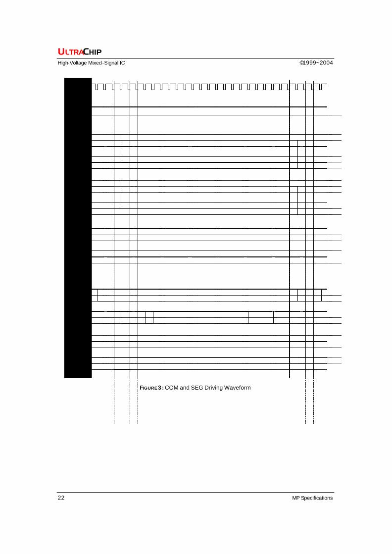
FIGURE 3 : COM and SEG Driving Waveform
UC1608 128x240 Matrix LCD Controller-Drivers
Revision 1.1 23
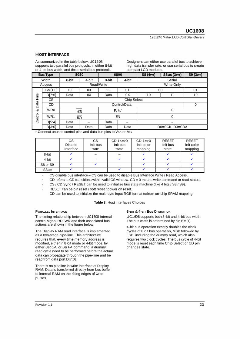
HOST INTERFACE As summarized in the table below, UC1608 supports two parallel bus protocols, in either 8-bit or 4-bit bus width, and three serial bus protocols.
Designers can either use parallel bus to achieve high data transfer rate, or use serial bus to create compact LCD modules.
Bus Type 8080 6800 S8 (4wr) S8uc (3wr) S9 (3wr)
Width 8-bit 4-bit 8-bit 4-bit Serial Access Read/Write Write Only
BM[1:0] 10 00 11 01 00 01 D[7:6] Data 0X Data 0X 10 11 10
CS Chip Select CD Control/Data 0
WR0 WR R/W 0
WR1 RD EN 0
D[5:4] Data – Data – – Con
trol &
Dat
a P
ins
D[3:0] Data Data Data Data D0=SCK, D3=SDA * Connect unused control pins and data bus pins to VDD or VSS
CS Disable Interface
CS Init bus state
CD 1<=>0 Init bus state
CD 1=>0 init color mapping
RESET Init bus state
RESET init color mapping
8-bit ü – – ü ü ü
4-bit ü – ü ü ü ü
S8 or S9 ü ü – ü ü ü
S8uc ü – ü ü ü ü
• CS disable bus interface – CS can be used to disable Bus Interface Write / Read Access. • CD refers to CD transitions within valid CS window. CD = 0 means write command or read status. • CS / CD Sync / RESET can be used to initialize bus state machine (like 4 bits / S8 / S9). • RESET can be pin reset / soft reset / power on reset.
CD can be used to initialize the multi-byte input RGB format to/from on-chip SRAM mapping.
Table 3: Host interfaces Choices
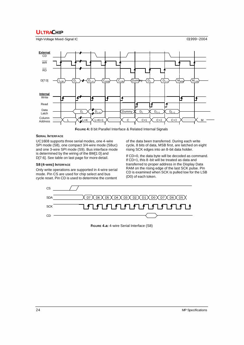
PARALLEL INTERFACE The timing relationship between UC1608 internal control signal RD, WR and their associated bus actions are shown in the figure below.
The Display RAM read interface is implemented as a two-stage pipe-line. This architecture requires that, every time memory address is modified, either in 8-bit mode or 4-bit mode, by either Set CA, or Set PA command, a dummy read cycle need to be performed before the actual data can propagate through the pipe-line and be read from data port D[7:0].
There is no pipeline in write interface of Display RAM. Data is transferred directly from bus buffer to internal RAM on the rising edges of write pulses.
8-BIT & 4-BIT BUS OPERATION UC1608 supports both 8 -bit and 4-bit bus width. The bus width is determined by pin BM[1].
4-bit bus operation exactly doubles the clock cycles of 8-bit bus operation, MSB followed by LSB, including the dummy read, which also requires two clock cycles. The bus cycle of 4-bit mode is reset each time Chip-Select or CD pin changes state.
ULTRACHIP
High-Voltage Mixed-Signal IC ©1999~2004
24 MP Specifications
LLSB DL DL+K CMSB CLSB Dummy DC DC+1 MMSB MLSB
L L+K L+K+1 C C+1 C+2 C+3 M
DL DL+K Dummy DC DC+1 DC+2
External CD ___ WR __ RD
D[7:0]
Internal Write
Read
Data Latch
Column Address
FIGURE 4: 8 bit Parallel Interface & Related Internal Signals
SERIAL INTERFACE
UC1608 supports three serial modes, one 4-wire SPI mode (S8), one compact 3/4-wire mode (S8uc) and one 3-wire SPI mode (S9). Bus interface mode is determined by the wiring of the BM[1:0] and D[7:6]. See table on last page for more detail.
S8 (4-WIRE) INTERFACE Only write operations are supported in 4-wire serial mode. Pin CS are used for chip select and bus cycle reset. Pin CD is used to determine the content
of the data been transferred. During each write cycle, 8 bits of data, MSB first, are latched on eight rising SCK edges into an 8-bit data holder.
If CD=0, the data byte will be decoded as command. If CD=1, this 8 -bit will be treated as data and transferred to proper address in the Display Data RAM on the rising edge of the last SCK pulse. Pin CD is examined when SCK is pulled low for the LSB (D0) of each token.
CS
SDA
SCK
CD
D7 D6 D5 D4 D3 D2 D1 D0 D7 D6 D5
FIGURE 4.a: 4-wire Serial Interface (S8)
UC1608 128x240 Matrix LCD Controller-Drivers
Revision 1.1 25
CS
SDA
SCK
CD
D7 D6 D5 D4 D3 D2 D1 D0 D7 D6 D5
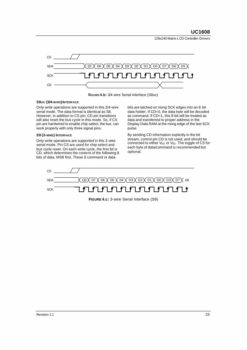
FIGURE 4.b: 3/4-wire Serial Interface (S8uc)
S8UC (3/4-WIRE) INTERFACE Only write operations are supported in this 3/4-wire serial mode. The data format is identical as S8. However, in addition to CS pin, CD pin transitions will also reset the bus cycle in this mode. So, if CS pin are hardwired to enable chip-select, the bus can work properly with only three signal pins.
S9 (3-WIRE) INTERFACE
Only write operations are supported in this 3-wire serial mode. Pin CS are used for chip select and bus cycle reset. On each write cycle, the first bit is CD, which determines the content of the following 8 bits of data, MSB first. These 8 command or data
bits are latched on rising SCK edges into an 8-bit data holder. If CD=0, the data byte will be decoded as command. If CD=1, this 8-bit will be treated as data and transferred to proper address in the Display Data RAM at the rising edge of the last SCK pulse.
By sending CD information explicitly in the bit stream, control pin CD is not used, and should be connected to either VDD or VSS. The toggle of CS for each byte of data/command is recommended but optional.
CS
SDA
SCK
CD D7 D6 D5 D4 D3 D2 D1 D0 CD D7 D6
FIGURE 4.c: 3-wire Serial Interface (S9)
ULTRACHIP
High-Voltage Mixed-Signal IC ©1999~2004
26 MP Specifications
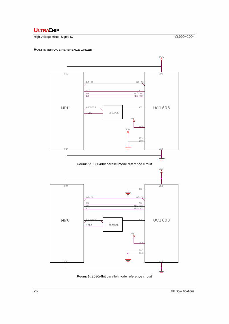
HOST INTERFACE REFERENCE CIRCUIT
IORQ
BM0
CDWRRD
VSS
UC1608
VDD
WR1(RD)
GND
CD
VDD
VDD
WR0(WR)
MPU
BM1
CSADDRESS
RST
D7-D0
VDD
DECODER
D7-D0
VCC
FIGURE 5 : 8080/8bit parallel mode reference circuit
CS
VDD
D7
CD
VDD
WR
UC1608
VSS
ADDRESS
IORQ
D3-D0
MPU
CD
BM1
RST
RD
D3-D0
DECODER
VCC
BM0
GND
VDD
WR1(RD)WR0(WR)
FIGURE 6: 8080/4bit parallel mode reference circuit
UC1608 128x240 Matrix LCD Controller-Drivers
Revision 1.1 27
CDWR0(R/W)
VCC
BM0
DECODER
E
VDD
D7-D0
R/W
RST
CSMPU
VSS
IORQ
VDD
GND
UC1608
VDD
CD
WR1(E)
BM1
VDD
ADDRESS
D7-D0
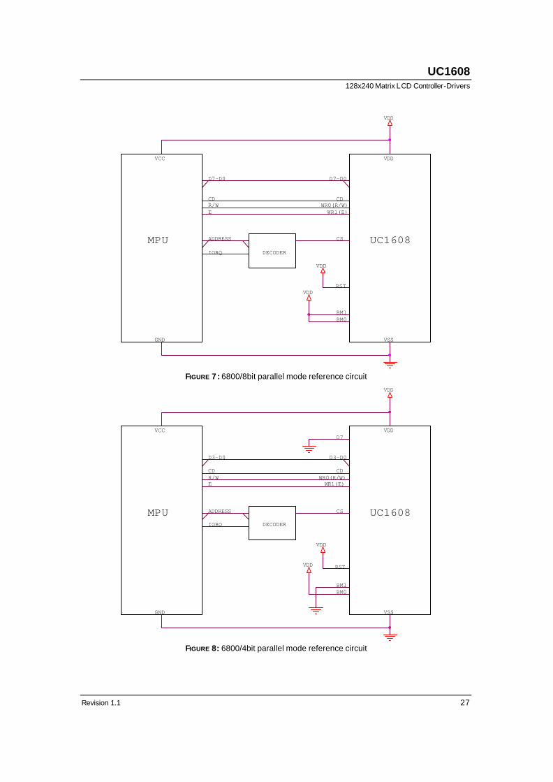
FIGURE 7 : 6800/8bit parallel mode reference circuit
VDD
DECODERIORQ
VSS
E WR1(E)
VCC
BM1BM0
ADDRESS
VDD
D7VDD
MPU
CD
VDD
D3-D0
CDR/W
UC1608
RST
GND
CS
WR0(R/W)
D3-D0
FIGURE 8: 6800/4bit parallel mode reference circuit
ULTRACHIP
High-Voltage Mixed-Signal IC ©1999~2004
28 MP Specifications
SDA(D3)
D7
ADDRESS
CD
CS
BM0BM1
DECODER
SCK
RST
VSSGND
SDA
D6
WR1
UC1608
VDD
MPU
CDWR0
SCK(D0)
VCC VDD
VDD
IORQ
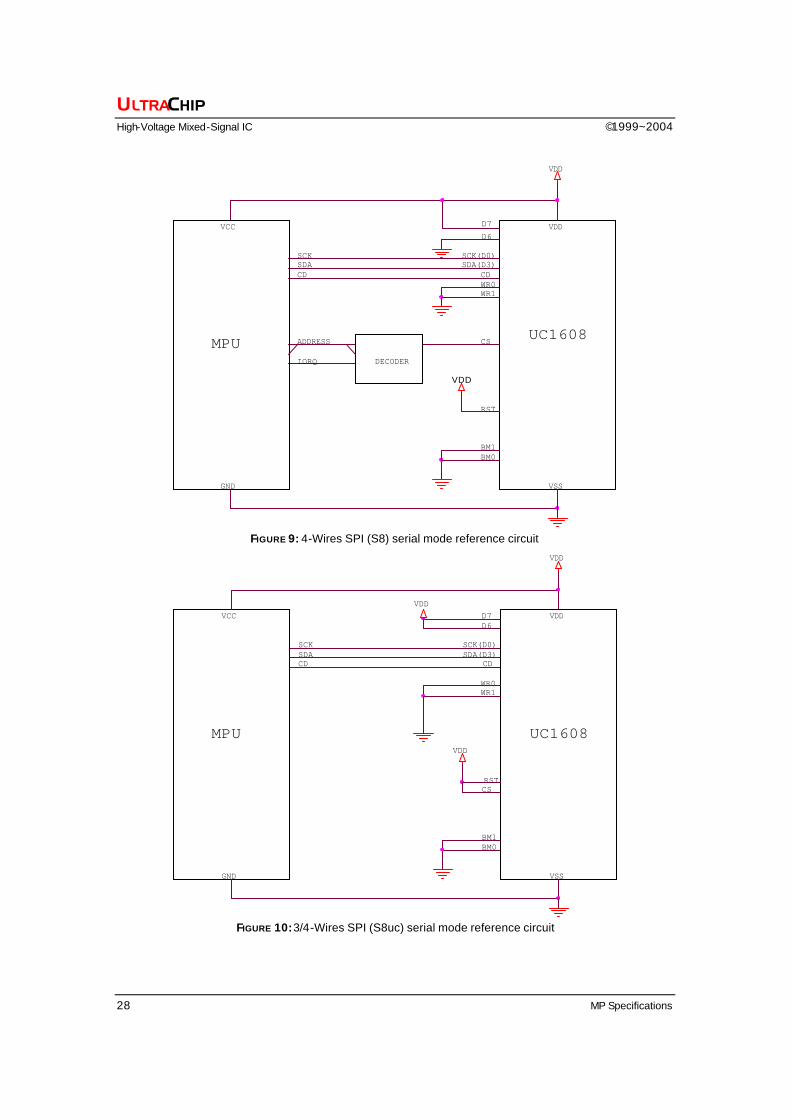
FIGURE 9: 4-Wires SPI (S8) serial mode reference circuit
BM0
SDA(D3)
VSS
SCK
WR0
VDD
CD
VDD
D7
WR1
RST
SDA
UC1608
CD
BM1
D6
VDDVCC
MPU
GND
VDD
SCK(D0)
CS
FIGURE 10: 3/4-Wires SPI (S8uc) serial mode reference circuit
UC1608 128x240 Matrix LCD Controller-Drivers
Revision 1.1 29
WR1
SCK(D0)
VDD
VDD
SDA(D3)
IORQ
MPU
VDD
ADDRESS
BM1
VSS
D7
SCK
VDD
UC1608
VDD
CS
RST
VCC
SDAWR0
D6
BM0
DECODER
GND
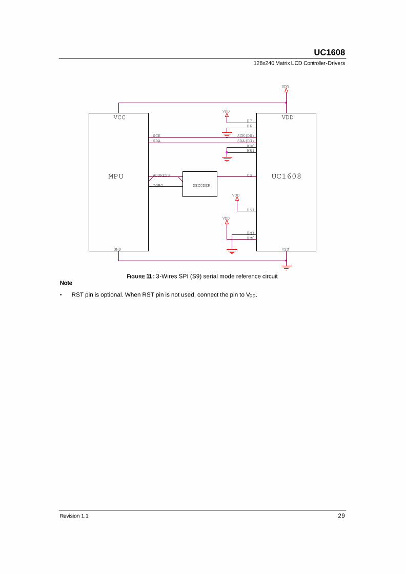
FIGURE 11 : 3-Wires SPI (S9) serial mode reference circuit
Note
• RST pin is optional. When RST pin is not used, connect the pin to VDD.
ULTRACHIP
High-Voltage Mixed-Signal IC ©1999~2004
30 MP Specifications
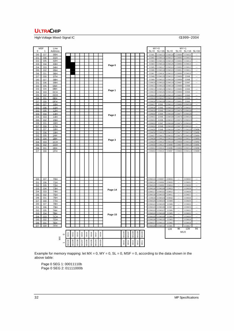
DISPLAY DATA RAM
DATA ORGANIZATION
The display data is 1-bit per pixel and stored in a dual port static RAM (RAM, for Display Data RAM). The RAM size is 128x240 for UC1608. This array of data bits is further organized into pages of 8 bit slices to facilitate parallel bus interface.
When Mirror X (MX, LC[2]) is OFF, the 1st column of LCD pixels will correspond to the bits of the first byte of each page, the 2nd column of LCD pixels correspond to the bits of the second byte of each page, etc.
MSB FIRST OR LSB FIRST
There are two options to map D[7:0] to RAM, MSB first (MSF=1), or LSB first (MSF=0), as illustrated in next page.
DISPLAY DATA RAM ACCESS The memory used in UC1608 Display Data RAM (RAM) is a special purpose dual port RAM which allows asynchronous access to both its column and row data. Thus, RAM can be independently accessed both for Host Interface and for display operations.
DISPLAY DATA RAM ADDRESSING
A Host Interface (HI) memory access operation starts with specifying Page Address (PA) and Column Address (CA) by issuing Set Page Address and Set Column Address commands.
If wrap-around (WA, AC[0]) is OFF (0), CA will stop increasing after reaching the end of page (239), and system programmers need to set the values of PA and CA explicitly.
If WA is ON (1), when CA reaches end of page, CA will be reset to 0 and PA will increment or decrement, depending on the setting of Page Increment Direction (PID, AC[2]). When PA reaches the boundary of RAM (i.e. PA = 0 or 19), PA will be wrapped around to the other end of RAM and continue.
MX IMPLEMENTATION
Column Mirroring (MX) is implemented by selecting either (CA) or (239–CA) as the RAM column address. Changing MX affects the data written to the RAM.
Since MX has no effect on data already stored in RAM, changing MX does not have immediate effect on the displayed pattern. To refresh the display, refresh the data stored in RAM after setting MX.
DISPLAY SCANNING During each field of display, depending on the setting of MR, COM electrodes will be scanned in a fixed pattern at a rate of
(Frame Rate x Mux Rate) rows/second.
During each row period, the signal at the SEG drivers determines the ON/OFF status of the row of pixels being scanned.
ROW SCANNING For each field, the scanning starts at COM1 through COMx, where x depends on the setting of MR.
COM electrode scanning (row scanning) orders are not affected by Start Line (SL) or Mirror Y (MY, LC[3]). When MY is 0, the effect of SL having a value K is to change the mapping of COM1 to the K-th bit slice of data stored in display RAM. Visually, SL having a non-zero value is equivalent to scrolling LCD display up by SL rows.
UC1608 128x240 Matrix LCD Controller-Drivers
Revision 1.1 31
RAM ADDRESS GENERATION The mapping of the data stored in the display SRAM and the scanning electrodes can be obtained by combining the fixed Row scanning sequence and the following RAM address generation formula.
During the display operation, the RAM line address generation can be mathematically represented as following:
For the 1st line period of each field Line = SL
Otherwise Line = Mod(Line+1, 128)
Where Mod is the modular operator, and Line is the bit slice line address of RAM to be outputted to SEG drivers. Line 0 corresponds to the first bit-slice of data in RAM.
The above Line generation formula produces the “loop around” effect as it effectively resets Line to 0 when Line+1 reaches 128.
Effects such as page scrolling can be emulated by changing SL dynamically.
MY IMPLEMENTATION Row Mirroring (MY) is implemented by reversing the mapping order between COM electrodes and RAM, i.e. the mathematical address generation formula becomes:
For the 1st line period of each field Line = Mod (SL + MUX-1, 128)
where MUX = 96 or 128.
Otherwise Line = Mod (Line - 1, 128)
Visually, the effect of MY is equivalent to flipping the display upside down. The data stored in display RAM is not affected by MY.
ULTRACHIP
High-Voltage Mixed-Signal IC ©1999~2004
32 MP Specifications
Line0 1 Address SL=0 SL=16 SL=0 SL=0 SL=16 SL=16
D0 D7 00H COM1 COM113 COM128 COM96 COM16 ---
D1 D6 01H COM2 COM114 COM127 COM95 COM15 ---
D2 D5 02H COM3 COM115 COM126 COM94 COM14 ---
D3 D4 03H COM4 COM116 COM125 COM93 COM13 ---
D4 D3 04H COM5 COM117 COM124 COM92 COM12 ---
D5 D2 05H COM6 COM118 COM123 COM91 COM11 ---
D6 D1 06H COM7 COM19 COM122 COM90 COM10 ---
D7 D0 07H COM8 COM120 COM121 COM89 COM9 ---
D0 D7 08H COM9 COM121 COM120 COM88 COM8 ---
D1 D6 09H COM10 COM122 COM119 COM87 COM7 ---
D2 D5 0AH COM11 COM123 COM118 COM86 COM6 ---
D3 D4 0BH COM12 COM124 COM117 COM85 COM5 ---
D4 D3 0CH COM13 COM125 COM116 COM84 COM4 ---
D5 D2 0DH COM14 COM126 COM115 COM83 COM3 ---
D6 D1 0EH COM15 COM127 COM114 COM82 COM2 ---
D7 D0 0FH COM16 COM128 COM113 COM81 COM1 ---
D0 D7 10H COM17 COM1 COM112 COM80 COM128 ---
D1 D6 11H COM18 COM2 COM111 COM79 COM127 ---
D2 D5 12H COM19 COM3 COM110 COM78 COM126 ---
D3 D4 13H COM20 COM4 COM109 COM77 COM125 ---
D4 D3 14H COM21 COM5 COM108 COM76 COM124 ---
D5 D2 15H COM22 COM6 COM107 COM75 COM123 ---
D6 D1 16H COM23 COM7 COM106 COM74 COM122 ---
D7 D0 17H COM24 COM8 COM105 COM73 COM121 ---
D0 D7 18H COM25 COM9 COM104 COM72 COM120 COM96
D1 D6 19H COM26 COM10 COM103 COM71 COM119 COM95
D2 D5 1AH COM27 COM11 COM102 COM70 COM118 COM94
D3 D4 1BH COM28 COM12 COM101 COM69 COM117 COM93
D4 D3 1CH COM29 COM13 COM100 COM68 COM116 COM92
D5 D2 1DH COM30 COM14 COM99 COM67 COM115 COM91
D6 D1 1EH COM31 COM15 COM98 COM66 COM114 COM90
D7 D0 1FH COM32 COM16 COM97 COM65 COM113 COM89
D0 D7 70H COM113 COM97 COM16 --- COM32 ---
D1 D6 71H COM114 COM98 COM15 --- COM31 ---
D2 D5 72H COM115 COM99 COM14 --- COM30 ---
D3 D4 73H COM116 COM100 COM13 --- COM29 ---
D4 D3 74H COM117 COM101 COM12 --- COM28 ---
D5 D2 75H COM118 COM102 COM11 --- COM27 ---
D6 D1 76H COM19 COM103 COM10 --- COM26 ---
D7 D0 77H COM120 COM104 COM9 --- COM25 ---
D0 D7 78H COM121 COM105 COM8 --- COM24 ---
D1 D6 79H COM122 COM106 COM7 --- COM23 ---
D2 D5 7AH COM123 COM107 COM6 --- COM22 ---
D3 D4 7BH COM124 COM108 COM5 --- COM21 ---
D4 D3 7CH COM125 COM109 COM4 --- COM20 ---
D5 D2 7DH COM126 COM110 COM3 --- COM19 ---
D6 D1 7EH COM127 COM111 COM2 --- COM18 ---
D7 D0 7FH COM128 COM112 COM1 --- COM17 ---
128 96 128 96
0
SE
G1
SE
G2
SE
G3
SE
G4
SE
G5
SE
G6
SE
G7
SE
G8
SE
G23
6
SE
G23
7
SE
G23
8
SE
G23
9
SE
G24
0
1
SE
G24
0
SE
G23
9
SE
G23
8
SE
G23
7
SE
G23
6
SE
G23
5
SE
G23
4
SE
G23
3
SE
G5
SE
G4
SE
G3
SE
G2
SE
G1M
X
MY=1
Page 15
Page 14
MY=0
MUX
Page 0
Page 1
Page 2
Page 3
MSF
Example for memory mapping: let MX = 0, MY = 0, SL = 0, MSF = 0, according to the data shown in the above table:
⇒ Page 0 SEG 1: 00011110b ⇒ Page 0 SEG 2: 01111000b
UC1608 128x240 Matrix LCD Controller-Drivers
Revision 1.1 33
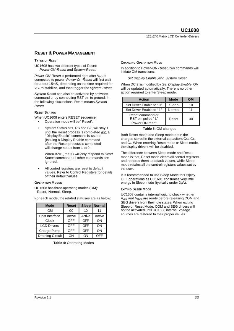
RESET & POWER MANAGEMENT
TYPES OF RESET
UC1608 has two different types of Reset: Power-ON-Reset and System -Reset.
Power-ON-Reset is performed right after VDD is connected to power. Power-On-Reset will first wait for about 15mS, depending on the time required for VDD to stabilize, and then trigger the System Reset.
System Reset can also be activated by software command or by connecting RST pin to ground. In the following discussions, Reset means System Reset.
RESET STATUS When UC1608 enters RESET sequence:
• Operation mode will be “Reset”.
• System Status bits, RS and BZ, will stay 1 until the Reset process is completed and a “Display Enable” command is issued. (Issuing a Display Enable command after the Reset process is completed will change status from 1 to 0.
When BZ=1, the IC will only respond to Read Status command; all other commands are ignored.
• All control registers are reset to default values. Refer to Control Registers for details of their default values.
OPERATION MODES
UC1608 has three operating modes (OM): Reset, Normal, Sleep.
For each mode, the related statuses are as below:
Mode Reset Sleep Normal OM 00 10 11
Host Interface Active Active Active Clock OFF OFF ON
LCD Drivers OFF OFF ON Charge Pump OFF OFF ON
Draining Circuit ON ON OFF
Table 4: Operating Modes
CHANGING OPERATION MODE
In addition to Power-ON-Reset, two commands will initiate OM transitions:
Set Display Enable , and System Reset.
When DC[2] is modified by Set Display Enable, OM will be updated automatically. There is no other action required to enter Sleep mode.
Action Mode OM
Set Driver Enable to “0” Sleep 10 Set Driver Enable to “1” Normal 11
Reset command or RST pin pulled “L” Power ON reset
Reset 00
Table 5: OM changes
Both Reset mode and Sleep mode drain the charges stored in the external capacitors CB0, CB1, and CL. When entering Reset mode or Sleep mode, the display drivers will be disabled.
The difference between Sleep mode and Reset mode is that, Reset mode clears all control registers and restores them to default values, while Sleep mode retains all the control registers values set by the user.
It is recommended to use Sleep Mode for Display OFF operations as UC1601 consumes very little energy in Sleep mode (typically under 2µA).
EXITING SLEEP MODE
UC1608 contains internal logic to check whether VLCD and VBIAS are ready before releasing COM and SEG drivers from their idle states. When exiting Sleep or Reset Mode, COM and SEG drivers will not be activated until UC1608 internal voltage sources are restored to their proper values.
ULTRACHIP
High-Voltage Mixed-Signal IC ©1999~2004
34 MP Specifications
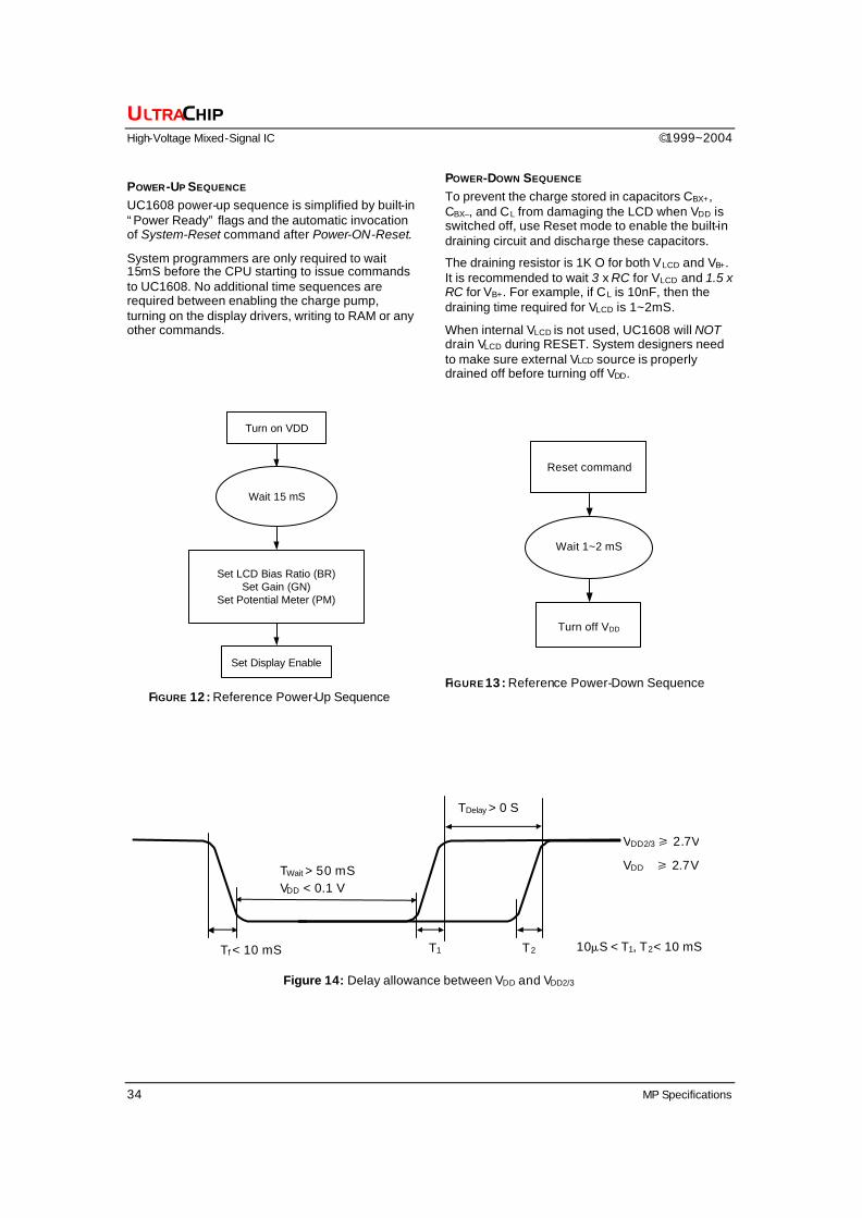
POWER-UP SEQUENCE UC1608 power-up sequence is simplified by built-in “Power Ready” flags and the automatic invocation of System-Reset command after Power-ON-Reset.
System programmers are only required to wait 15mS before the CPU starting to issue commands to UC1608. No additional time sequences are required between enabling the charge pump, turning on the display drivers, writing to RAM or any other commands.
POWER-DOWN SEQUENCE To prevent the charge stored in capacitors CBX+, CBX–, and CL from damaging the LCD when VDD is switched off, use Reset mode to enable the built-in draining circuit and discharge these capacitors.
The draining resistor is 1K O for both VLCD and VB+. It is recommended to wait 3 x RC for VLCD and 1.5 x RC for VB+. For example, if CL is 10nF, then the draining time required for VLCD is 1~2mS.
When internal VLCD is not used, UC1608 will NOT drain VLCD during RESET. System designers need to make sure external VLCD source is properly drained off before turning off VDD.
Turn on VDD
Set LCD Bias Ratio (BR)
Set Gain (GN) Set Potential Meter (PM)
Set Display Enable
Wait 15 mS
FIGURE 12 : Reference Power-Up Sequence
Turn off VDD
Reset command
Wait 1~2 mS
FIGURE 13 : Reference Power-Down Sequence
Figure 14: Delay allowance between VDD and VDD2/3
TDelay > 0 S
VDD2/3 / 2.7V
VDD / 2.7V
10µS < T1, T2 < 10 mS T1 T2
TWait > 50 mS VDD < 0.1 V
Tf < 10 mS
UC1608 128x240 Matrix LCD Controller-Drivers
Revision 1.1 35
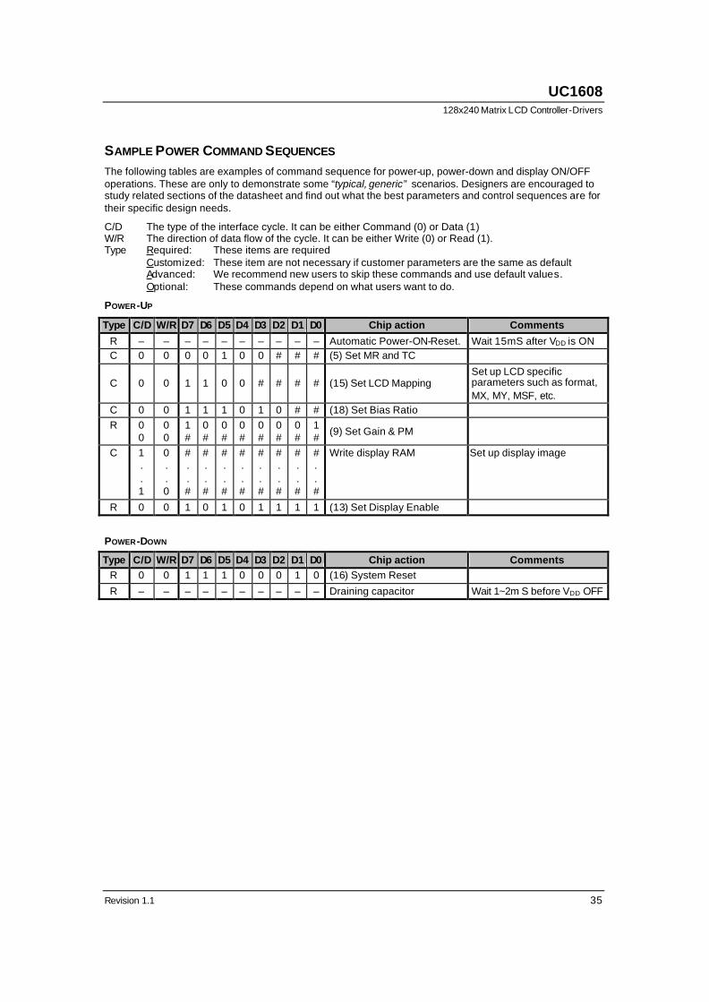
SAMPLE POWER COMMAND SEQUENCES The following tables are examples of command sequence for power-up, power-down and display ON/OFF operations. These are only to demonstrate some “typical, generic” scenarios. Designers are encouraged to study related sections of the datasheet and find out what the best parameters and control sequences are for their specific design needs.
C/D The type of the interface cycle. It can be either Command (0) or Data (1) W/R The direction of data flow of the cycle. It can be either Write (0) or Read (1). Type Required: These items are required
Customized: These item are not necessary if customer parameters are the same as default Advanced: We recommend new users to skip these commands and use default values. Optional: These commands depend on what users want to do.
POWER-UP
Type C/D W/R D7 D6 D5 D4 D3 D2 D1 D0 Chip action Comments
R – – – – – – – – – – Automatic Power-ON-Reset. Wait 15mS after VDD is ON C 0 0 0 0 1 0 0 # # # (5) Set MR and TC
C 0 0 1 1 0 0 # # # # (15) Set LCD Mapping Set up LCD specific parameters such as format, MX, MY, MSF, etc.
C 0 0 1 1 1 0 1 0 # # (18) Set Bias Ratio R 0
0 0 0
1 #
0 #
0 #
0 #
0 #
0 #
0 #
1 # (9) Set Gain & PM
C 1 . . 1
0 . . 0
# . . #
# . . #
# . . #
# . . #
# . . #
# . . #
# . . #
# . . #
Write display RAM Set up display image
R 0 0 1 0 1 0 1 1 1 1 (13) Set Display Enable
POWER-DOWN
Type C/D W/R D7 D6 D5 D4 D3 D2 D1 D0 Chip action Comments R 0 0 1 1 1 0 0 0 1 0 (16) System Reset
R – – – – – – – – – – Draining capacitor Wait 1~2m S before VDD OFF
ULTRACHIP
High-Voltage Mixed-Signal IC ©1999~2004
36 MP Specifications
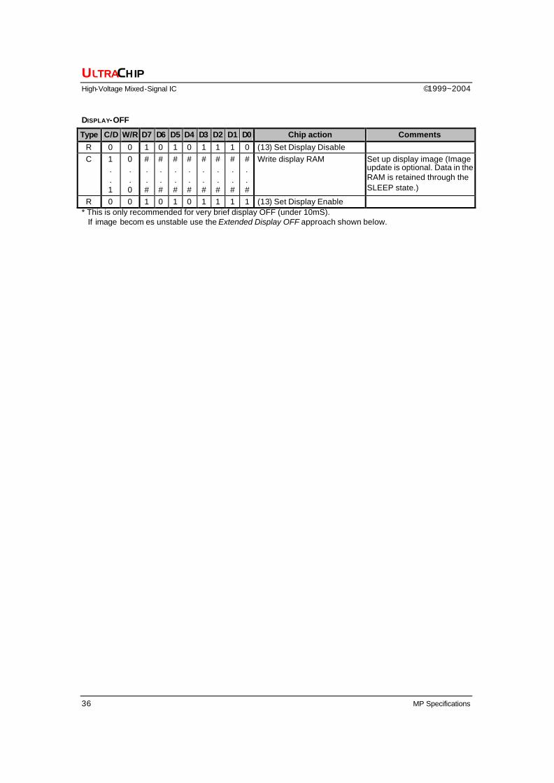
DISPLAY-OFF
Type C/D W/R D7 D6 D5 D4 D3 D2 D1 D0 Chip action Comments
R 0 0 1 0 1 0 1 1 1 0 (13) Set Display Disable C 1
.
. 1
0 . . 0
# . . #
# . . #
# . . #
# . . #
# . . #
# . . #
# . . #
# . . #
Write display RAM Set up display image (Image update is optional. Data in the RAM is retained through the SLEEP state.)
R 0 0 1 0 1 0 1 1 1 1 (13) Set Display Enable * This is only recommended for very brief display OFF (under 10mS). If image becom es unstable use the Extended Display OFF approach shown below.
UC1608 128x240 Matrix LCD Controller-Drivers
Revision 1.1 37
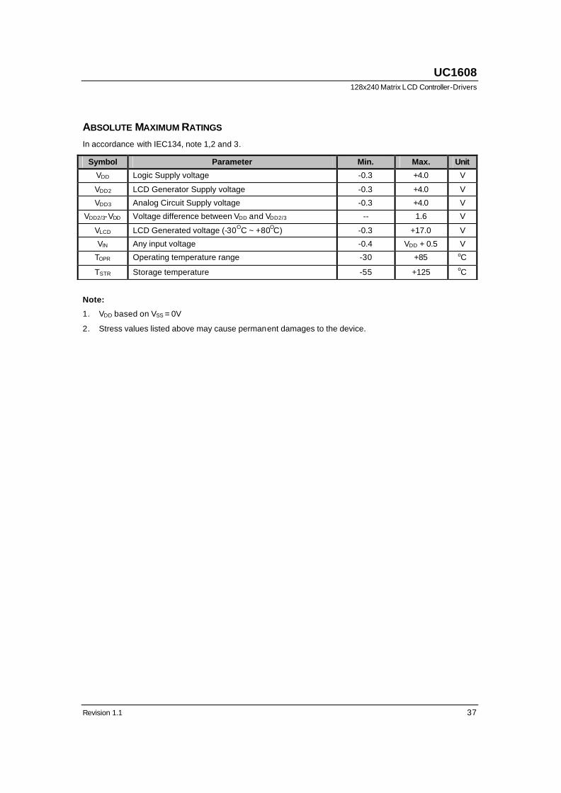
ABSOLUTE MAXIMUM RATINGS In accordance with IEC134, note 1,2 and 3.
Symbol Parameter Min. Max. Unit
VDD Logic Supply voltage -0.3 +4.0 V
VDD2 LCD Generator Supply voltage -0.3 +4.0 V
VDD3 Analog Circuit Supply voltage -0.3 +4.0 V
VDD2/3-VDD Voltage difference between VDD and VDD2/3 -- 1.6 V
VLCD LCD Generated voltage (-30OC ~ +80OC) -0.3 +17.0 V
VIN Any input voltage -0.4 VDD + 0.5 V
TOPR Operating temperature range -30 +85 oC
TSTR Storage temperature -55 +125 oC
Note:
1. VDD based on VSS = 0V
2. Stress values listed above may cause permanent damages to the device.
ULTRACHIP
High-Voltage Mixed-Signal IC ©1999~2004
38 MP Specifications
SPECIFICATIONS
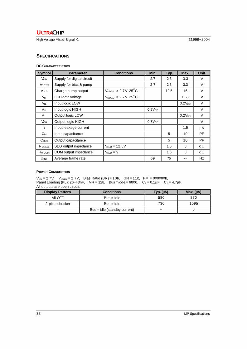
DC CHARACTERISTICS
Symbol Parameter Conditions Min. Typ. Max. Unit
VDD Supply for digital circuit 2.7 2.8 3.3 V
VDD2/3 Supply for bias & pump 2.7 2.8 3.3 V
VLCD Charge pump output VDD2/3 / 2.7V, 25OC 12.5 16 V
VD LCD data voltage VDD2/3 / 2.7V, 25OC 1.53 V
VIL Input logic LOW 0.2VDD V
VIH Input logic HIGH 0.8VDD V
VOL Output logic LOW 0.2VDD V
VOH Output logic HIGH 0.8VDD V
IIL Input leakage current 1.5 µA
CIN Input capacitance 5 10 PF
COUT Output capacitance 5 10 PF
R0(SEG) SEG output impedance VLCD = 12.5V 1.5 3 k O
R0(COM) COM output impedance VLCD = 9 1.5 3 k O
fLINE Average frame rate 69 75 -- Hz
POWER CONSUMPTION
VDD = 2.7V, VDD2/3 = 2.7V, Bias Ratio (BR) = 10b, GN = 11b, PM = 000000b, Panel Loading (PL): 26~43nF, MR = 128, Bus m ode = 6800, CL = 0.1µF, CB = 4.7µF. All outputs are open circuit.
Display Pattern Conditions Typ. (µA) Max. (µA)
All-OFF Bus = idle 580 870
2-pixel checker Bus = idle 730 1095
-- Bus = idle (standby current) -- 5
UC1608 128x240 Matrix LCD Controller-Drivers
Revision 1.1 39
AC CHARACTERISTICS
FIGURE 15 : Parallel Bus Timing Characteristics (for 8080 MCU)
(2.7V £ VDD < 3.3V, Ta= –30 to +85
oC)
Symbol Signal Description Condition Min. Max. Units tAS80
tAH80 CD Address setup time
Address hold time 0
20 – nS
tCY80 System cycle time 8 bits bus (read) (write) 4 bits bus (read) (write)
140 140 140 140
– nS
tPWR80 WR1 Pulse width 8 bits (read) 4 bits
65 65
– nS
tPWW80 WR0 Pulse width 8 bits (write) 4 bits
35 35
– nS
tHPW80 WR0, WR1 High pulse width 8 bits bus (read) (write) 4 bits bus (read) (write)
65 35 65 35
– nS
tDS80
tDH80 D0~D7 Data setup time
Data hold time 30
20 – nS
tACC80
tOD80 Read access time
Output disable time CL = 100pF –
12 60 20
nS
tSSA80 tCSSD80 tCSH80
CS1/CS0 Chip select setup time 10 10 20
nS
CD
tAS80 tAH80 CS tCSSA80 tCY80 tCSH80 tCSSD80
tPWR80, tPWW80 tHPW80 WR0, WR1
tDS80 tDH80
Write D[7:0] tACC80 tOD80
Read D[7:0]
ULTRACHIP
High-Voltage Mixed-Signal IC ©1999~2004
40 MP Specifications
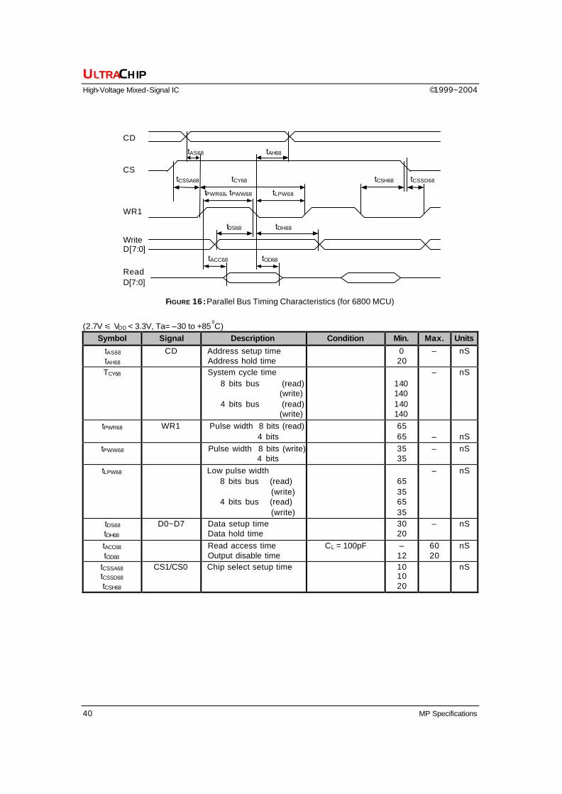
FIGURE 16 : Parallel Bus Timing Characteristics (for 6800 MCU)
(2.7V £ VDD < 3.3V, Ta= –30 to +85
oC)
Symbol Signal Description Condition Min. Max. Units
tAS68
tAH68 CD Address setup time
Address hold time 0
20 – nS
TCY68 System cycle time 8 bits bus (read) (write) 4 bits bus (read) (write)
140 140 140 140
– nS
tPWR68 WR1 Pulse width 8 bits (read) 4 bits
65 65
–
nS
tPWW68 Pulse width 8 bits (write) 4 bits
35 35
– nS
tLPW68 Low pulse width 8 bits bus (read) (write) 4 bits bus (read) (write)
65 35 65 35
– nS
tDS68
tDH68 D0~D7 Data setup time
Data hold time 30
20 – nS
tACC68
tOD68 Read access time
Output disable time CL = 100pF –
12 60 20
nS
tCSSA68 tCSSD68 tCSH68
CS1/CS0 Chip select setup time 10 10 20
nS
CD
tAS68 tAH68 CS tCSSA68 tCY68 tCSH68 tCSSD68
tPWR68, tPWW68 tLPW68 WR1
tDS68 tDH68
Write D[7:0] tACC68 tOD68
Read D[7:0]
UC1608 128x240 Matrix LCD Controller-Drivers
Revision 1.1 41
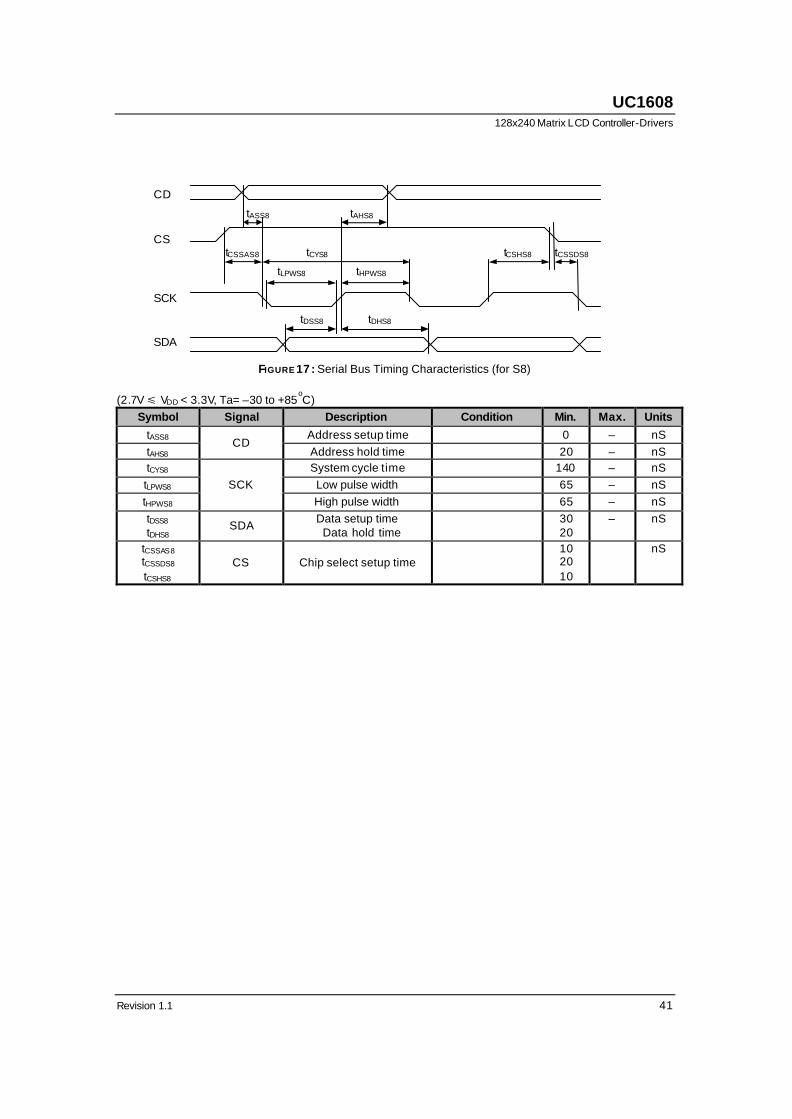
FIGURE 17 : Serial Bus Timing Characteristics (for S8)
(2.7V £ VDD < 3.3V, Ta= –30 to +85
oC)
Symbol Signal Description Condition Min. Max. Units
tASS8 Address setup time 0 – nS tAHS8
CD Address hold time 20 – nS
tCYS8 System cycle time 140 – nS tLPWS8 Low pulse width 65 – nS tHPWS8
SCK High pulse width 65 – nS
tDSS8
tDHS8 SDA Data setup time Data hold time
30 20
– nS
tCSSAS8 tCSSDS8 tCSHS8
CS Chip select setup time 10
20 10
nS
CD
tASS8 tAHS8 CS tCSSAS8 tCYS8 tCSHS8 tCSSDS8
tLPWS8 tHPWS8 SCK
tDSS8 tDHS8
SDA
ULTRACHIP
High-Voltage Mixed-Signal IC ©1999~2004
42 MP Specifications
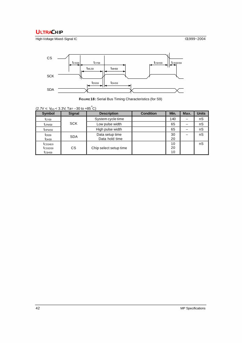
FIGURE 18 : Serial Bus Timing Characteristics (for S9)
(2.7V £ VDD < 3.3V, Ta= –30 to +85oC)
Symbol Signal Description Condition Min. Max. Units
tCYS9 System cycle time 140 – nS tLPWS9 Low pulse width 65 – nS tHPWS9
SCK
High pulse width 65 – nS tDSS9
tDHS9 SDA Data setup time Data hold time
30 20
– nS
tCSSAS9 tCSSDS9 tCSHS9
CS Chip select setup time 10
20 10
nS
CS tCSS9 tCYS9 tCSHS9 tCSSDS9
tWLS9 tWHS9 SCK
tDSS9 tDHS9
SDA
UC1608 128x240 Matrix LCD Controller-Drivers
Revision 1.1 43
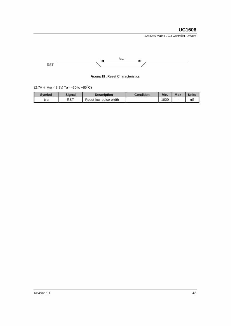
RST
tRW
FIGURE 19 : Reset Characteristics
(2.7V £ VDD < 3.3V, Ta= –30 to +85oC)
Symbol Signal Description Condition Min. Max. Units tRW RST Reset low pulse width 1000 – nS
ULTRACHIP
High-Voltage Mixed-Signal IC ©1999~2004
44 MP Specifications
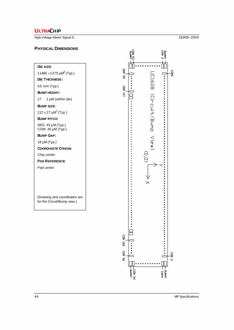
PHYSICAL DIMENSIONS
DIE SIZE:
11480 X 1375 µM2 (Typ.)
DIE THICKNESS:
0.5 mm (Typ.)
BUMP HEIGHT:
17 ± 1 µM (within die)
BUMP SIZE:
112 x 27 µM2 (Typ.)
BUMP PITCH:
SEG: 45 µ M (Typ.) COM: 45 µM (Typ.)
BUMP GAP:
18 µM (Typ.)
COORDINATE ORIGIN:
Chip center
PAD REFERENCE:
Pad center
(Drawing and coordinates are for the Circuit/Bump view.)
UC1608 128x240 Matrix LCD Controller-Drivers
Revision 1.1 45
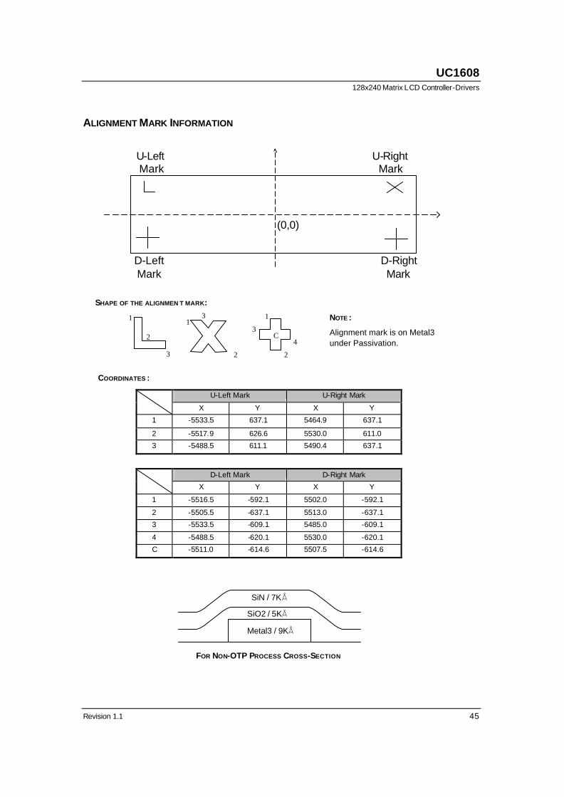
ALIGNMENT MARK INFORMATION
FOR NON-OTP PROCESS CROSS-SECTION
Metal3 / 9KÅ
SiO2 / 5KÅ
SiN / 7KÅ
Mark Mark
SHAPE OF THE ALIGNMEN T MARK:
COORDINATES :
U-Left Mark U-Right Mark X Y X Y
1 -5533.5 637.1 5464.9 637.1
2 -5517.9 626.6 5530.0 611.0
3 -5488.5 611.1 5490.4 637.1
D-Left Mark D-Right Mark
X Y X Y
1 -5516.5 -592.1 5502.0 -592.1
2 -5505.5 -637.1 5513.0 -637.1
3 -5533.5 -609.1 5485.0 -609.1
4 -5488.5 -620.1 5530.0 -620.1
C -5511.0 -614.6 5507.5 -614.6
(0,0)
D-Left D-Right
U-Left Mark
U-Right Mark
NOTE :
Alignment mark is on Metal3 under Passivation.
1
2
3
1
2
3 1
2
3 4 C
ULTRACHIP
High-Voltage Mixed-Signal IC ©1999~2004
46 MP Specifications
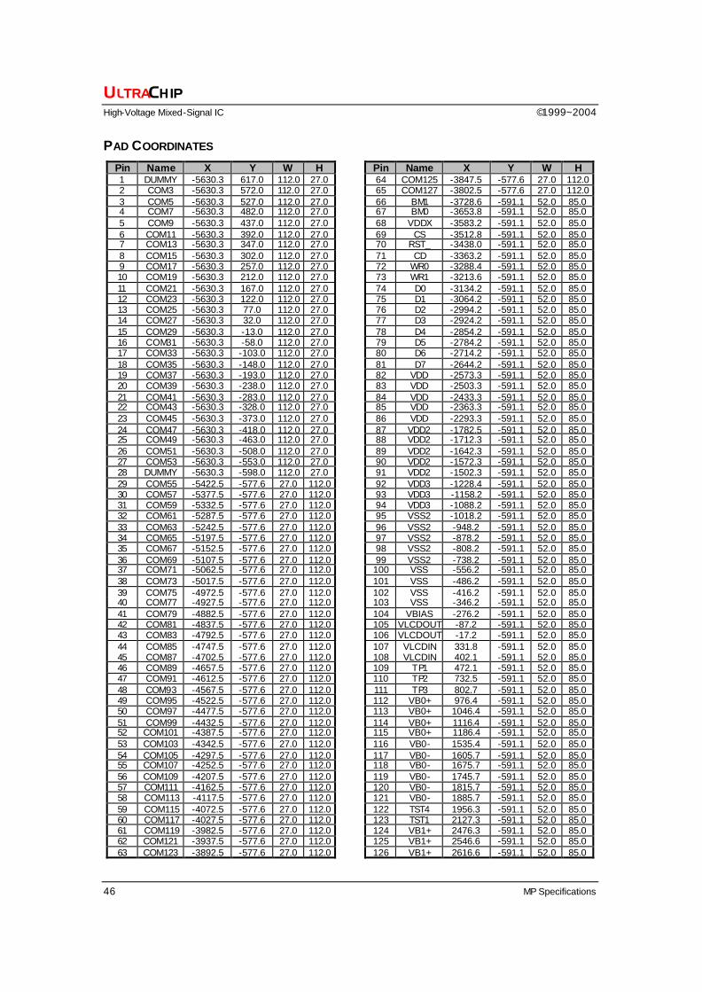
PAD COORDINATES
Pin Name X Y W H 1 DUMMY -5630.3 617.0 112.0 27.0 2 COM3 -5630.3 572.0 112.0 27.0 3 COM5 -5630.3 527.0 112.0 27.0 4 COM7 -5630.3 482.0 112.0 27.0 5 COM9 -5630.3 437.0 112.0 27.0 6 COM11 -5630.3 392.0 112.0 27.0 7 COM13 -5630.3 347.0 112.0 27.0 8 COM15 -5630.3 302.0 112.0 27.0 9 COM17 -5630.3 257.0 112.0 27.0 10 COM19 -5630.3 212.0 112.0 27.0 11 COM21 -5630.3 167.0 112.0 27.0 12 COM23 -5630.3 122.0 112.0 27.0 13 COM25 -5630.3 77.0 112.0 27.0 14 COM27 -5630.3 32.0 112.0 27.0 15 COM29 -5630.3 -13.0 112.0 27.0 16 COM31 -5630.3 -58.0 112.0 27.0 17 COM33 -5630.3 -103.0 112.0 27.0 18 COM35 -5630.3 -148.0 112.0 27.0 19 COM37 -5630.3 -193.0 112.0 27.0 20 COM39 -5630.3 -238.0 112.0 27.0 21 COM41 -5630.3 -283.0 112.0 27.0 22 COM43 -5630.3 -328.0 112.0 27.0 23 COM45 -5630.3 -373.0 112.0 27.0 24 COM47 -5630.3 -418.0 112.0 27.0 25 COM49 -5630.3 -463.0 112.0 27.0 26 COM51 -5630.3 -508.0 112.0 27.0 27 COM53 -5630.3 -553.0 112.0 27.0 28 DUMMY -5630.3 -598.0 112.0 27.0 29 COM55 -5422.5 -577.6 27.0 112.0 30 COM57 -5377.5 -577.6 27.0 112.0 31 COM59 -5332.5 -577.6 27.0 112.0 32 COM61 -5287.5 -577.6 27.0 112.0 33 COM63 -5242.5 -577.6 27.0 112.0 34 COM65 -5197.5 -577.6 27.0 112.0 35 COM67 -5152.5 -577.6 27.0 112.0 36 COM69 -5107.5 -577.6 27.0 112.0 37 COM71 -5062.5 -577.6 27.0 112.0 38 COM73 -5017.5 -577.6 27.0 112.0 39 COM75 -4972.5 -577.6 27.0 112.0 40 COM77 -4927.5 -577.6 27.0 112.0 41 COM79 -4882.5 -577.6 27.0 112.0 42 COM81 -4837.5 -577.6 27.0 112.0 43 COM83 -4792.5 -577.6 27.0 112.0 44 COM85 -4747.5 -577.6 27.0 112.0 45 COM87 -4702.5 -577.6 27.0 112.0 46 COM89 -4657.5 -577.6 27.0 112.0 47 COM91 -4612.5 -577.6 27.0 112.0 48 COM93 -4567.5 -577.6 27.0 112.0 49 COM95 -4522.5 -577.6 27.0 112.0 50 COM97 -4477.5 -577.6 27.0 112.0 51 COM99 -4432.5 -577.6 27.0 112.0 52 COM101 -4387.5 -577.6 27.0 112.0 53 COM103 -4342.5 -577.6 27.0 112.0 54 COM105 -4297.5 -577.6 27.0 112.0 55 COM107 -4252.5 -577.6 27.0 112.0 56 COM109 -4207.5 -577.6 27.0 112.0 57 COM111 -4162.5 -577.6 27.0 112.0 58 COM113 -4117.5 -577.6 27.0 112.0 59 COM115 -4072.5 -577.6 27.0 112.0 60 COM117 -4027.5 -577.6 27.0 112.0 61 COM119 -3982.5 -577.6 27.0 112.0 62 COM121 -3937.5 -577.6 27.0 112.0 63 COM123 -3892.5 -577.6 27.0 112.0
Pin Name X Y W H 64 COM125 -3847.5 -577.6 27.0 112.0 65 COM127 -3802.5 -577.6 27.0 112.0 66 BM1 -3728.6 -591.1 52.0 85.0 67 BM0 -3653.8 -591.1 52.0 85.0 68 VDDX -3583.2 -591.1 52.0 85.0 69 CS -3512.8 -591.1 52.0 85.0 70 RST_ -3438.0 -591.1 52.0 85.0 71 CD -3363.2 -591.1 52.0 85.0 72 WR0 -3288.4 -591.1 52.0 85.0 73 WR1 -3213.6 -591.1 52.0 85.0 74 D0 -3134.2 -591.1 52.0 85.0 75 D1 -3064.2 -591.1 52.0 85.0 76 D2 -2994.2 -591.1 52.0 85.0 77 D3 -2924.2 -591.1 52.0 85.0 78 D4 -2854.2 -591.1 52.0 85.0 79 D5 -2784.2 -591.1 52.0 85.0 80 D6 -2714.2 -591.1 52.0 85.0 81 D7 -2644.2 -591.1 52.0 85.0 82 VDD -2573.3 -591.1 52.0 85.0 83 VDD -2503.3 -591.1 52.0 85.0 84 VDD -2433.3 -591.1 52.0 85.0 85 VDD -2363.3 -591.1 52.0 85.0 86 VDD -2293.3 -591.1 52.0 85.0 87 VDD2 -1782.5 -591.1 52.0 85.0 88 VDD2 -1712.3 -591.1 52.0 85.0 89 VDD2 -1642.3 -591.1 52.0 85.0 90 VDD2 -1572.3 -591.1 52.0 85.0 91 VDD2 -1502.3 -591.1 52.0 85.0 92 VDD3 -1228.4 -591.1 52.0 85.0 93 VDD3 -1158.2 -591.1 52.0 85.0 94 VDD3 -1088.2 -591.1 52.0 85.0 95 VSS2 -1018.2 -591.1 52.0 85.0 96 VSS2 -948.2 -591.1 52.0 85.0 97 VSS2 -878.2 -591.1 52.0 85.0 98 VSS2 -808.2 -591.1 52.0 85.0 99 VSS2 -738.2 -591.1 52.0 85.0
100 VSS -556.2 -591.1 52.0 85.0 101 VSS -486.2 -591.1 52.0 85.0 102 VSS -416.2 -591.1 52.0 85.0 103 VSS -346.2 -591.1 52.0 85.0 104 VBIAS -276.2 -591.1 52.0 85.0 105 VLCDOUT -87.2 -591.1 52.0 85.0 106 VLCDOUT -17.2 -591.1 52.0 85.0 107 VLCDIN 331.8 -591.1 52.0 85.0 108 VLCDIN 402.1 -591.1 52.0 85.0 109 TP1 472.1 -591.1 52.0 85.0 110 TP2 732.5 -591.1 52.0 85.0 111 TP3 802.7 -591.1 52.0 85.0 112 VB0+ 976.4 -591.1 52.0 85.0 113 VB0+ 1046.4 -591.1 52.0 85.0 114 VB0+ 1116.4 -591.1 52.0 85.0 115 VB0+ 1186.4 -591.1 52.0 85.0 116 VB0- 1535.4 -591.1 52.0 85.0 117 VB0- 1605.7 -591.1 52.0 85.0 118 VB0- 1675.7 -591.1 52.0 85.0 119 VB0- 1745.7 -591.1 52.0 85.0 120 VB0- 1815.7 -591.1 52.0 85.0 121 VB0- 1885.7 -591.1 52.0 85.0 122 TST4 1956.3 -591.1 52.0 85.0 123 TST1 2127.3 -591.1 52.0 85.0 124 VB1+ 2476.3 -591.1 52.0 85.0 125 VB1+ 2546.6 -591.1 52.0 85.0 126 VB1+ 2616.6 -591.1 52.0 85.0
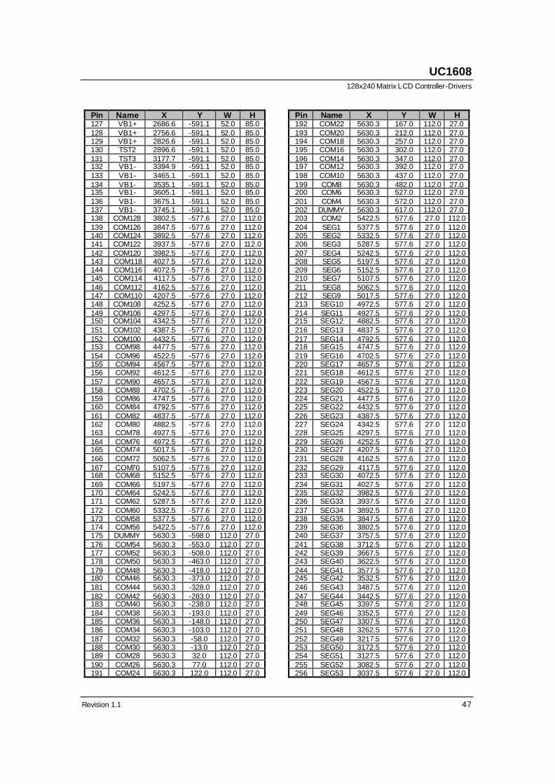
UC1608 128x240 Matrix LCD Controller-Drivers
Revision 1.1 47
Pin Name X Y W H 127 VB1+ 2686.6 -591.1 52.0 85.0 128 VB1+ 2756.6 -591.1 52.0 85.0 129 VB1+ 2826.6 -591.1 52.0 85.0 130 TST2 2896.6 -591.1 52.0 85.0 131 TST3 3177.7 -591.1 52.0 85.0 132 VB1- 3394.9 -591.1 52.0 85.0 133 VB1- 3465.1 -591.1 52.0 85.0 134 VB1- 3535.1 -591.1 52.0 85.0 135 VB1- 3605.1 -591.1 52.0 85.0 136 VB1- 3675.1 -591.1 52.0 85.0 137 VB1- 3745.1 -591.1 52.0 85.0 138 COM128 3802.5 -577.6 27.0 112.0 139 COM126 3847.5 -577.6 27.0 112.0 140 COM124 3892.5 -577.6 27.0 112.0 141 COM122 3937.5 -577.6 27.0 112.0 142 COM120 3982.5 -577.6 27.0 112.0 143 COM118 4027.5 -577.6 27.0 112.0 144 COM116 4072.5 -577.6 27.0 112.0 145 COM114 4117.5 -577.6 27.0 112.0 146 COM112 4162.5 -577.6 27.0 112.0 147 COM110 4207.5 -577.6 27.0 112.0 148 COM108 4252.5 -577.6 27.0 112.0 149 COM106 4297.5 -577.6 27.0 112.0 150 COM104 4342.5 -577.6 27.0 112.0 151 COM102 4387.5 -577.6 27.0 112.0 152 COM100 4432.5 -577.6 27.0 112.0 153 COM98 4477.5 -577.6 27.0 112.0 154 COM96 4522.5 -577.6 27.0 112.0 155 COM94 4567.5 -577.6 27.0 112.0 156 COM92 4612.5 -577.6 27.0 112.0 157 COM90 4657.5 -577.6 27.0 112.0 158 COM88 4702.5 -577.6 27.0 112.0 159 COM86 4747.5 -577.6 27.0 112.0 160 COM84 4792.5 -577.6 27.0 112.0 161 COM82 4837.5 -577.6 27.0 112.0 162 COM80 4882.5 -577.6 27.0 112.0 163 COM78 4927.5 -577.6 27.0 112.0 164 COM76 4972.5 -577.6 27.0 112.0 165 COM74 5017.5 -577.6 27.0 112.0 166 COM72 5062.5 -577.6 27.0 112.0 167 COM70 5107.5 -577.6 27.0 112.0 168 COM68 5152.5 -577.6 27.0 112.0 169 COM66 5197.5 -577.6 27.0 112.0 170 COM64 5242.5 -577.6 27.0 112.0 171 COM62 5287.5 -577.6 27.0 112.0 172 COM60 5332.5 -577.6 27.0 112.0 173 COM58 5377.5 -577.6 27.0 112.0 174 COM56 5422.5 -577.6 27.0 112.0 175 DUMMY 5630.3 -598.0 112.0 27.0 176 COM54 5630.3 -553.0 112.0 27.0 177 COM52 5630.3 -508.0 112.0 27.0 178 COM50 5630.3 -463.0 112.0 27.0 179 COM48 5630.3 -418.0 112.0 27.0 180 COM46 5630.3 -373.0 112.0 27.0 181 COM44 5630.3 -328.0 112.0 27.0 182 COM42 5630.3 -283.0 112.0 27.0 183 COM40 5630.3 -238.0 112.0 27.0 184 COM38 5630.3 -193.0 112.0 27.0 185 COM36 5630.3 -148.0 112.0 27.0 186 COM34 5630.3 -103.0 112.0 27.0 187 COM32 5630.3 -58.0 112.0 27.0 188 COM30 5630.3 -13.0 112.0 27.0 189 COM28 5630.3 32.0 112.0 27.0 190 COM26 5630.3 77.0 112.0 27.0 191 COM24 5630.3 122.0 112.0 27.0
Pin Name X Y W H 192 COM22 5630.3 167.0 112.0 27.0 193 COM20 5630.3 212.0 112.0 27.0 194 COM18 5630.3 257.0 112.0 27.0 195 COM16 5630.3 302.0 112.0 27.0 196 COM14 5630.3 347.0 112.0 27.0 197 COM12 5630.3 392.0 112.0 27.0 198 COM10 5630.3 437.0 112.0 27.0 199 COM8 5630.3 482.0 112.0 27.0 200 COM6 5630.3 527.0 112.0 27.0 201 COM4 5630.3 572.0 112.0 27.0 202 DUMMY 5630.3 617.0 112.0 27.0 203 COM2 5422.5 577.6 27.0 112.0 204 SEG1 5377.5 577.6 27.0 112.0 205 SEG2 5332.5 577.6 27.0 112.0 206 SEG3 5287.5 577.6 27.0 112.0 207 SEG4 5242.5 577.6 27.0 112.0 208 SEG5 5197.5 577.6 27.0 112.0 209 SEG6 5152.5 577.6 27.0 112.0 210 SEG7 5107.5 577.6 27.0 112.0 211 SEG8 5062.5 577.6 27.0 112.0 212 SEG9 5017.5 577.6 27.0 112.0 213 SEG10 4972.5 577.6 27.0 112.0 214 SEG11 4927.5 577.6 27.0 112.0 215 SEG12 4882.5 577.6 27.0 112.0 216 SEG13 4837.5 577.6 27.0 112.0 217 SEG14 4792.5 577.6 27.0 112.0 218 SEG15 4747.5 577.6 27.0 112.0 219 SEG16 4702.5 577.6 27.0 112.0 220 SEG17 4657.5 577.6 27.0 112.0 221 SEG18 4612.5 577.6 27.0 112.0 222 SEG19 4567.5 577.6 27.0 112.0 223 SEG20 4522.5 577.6 27.0 112.0 224 SEG21 4477.5 577.6 27.0 112.0 225 SEG22 4432.5 577.6 27.0 112.0 226 SEG23 4387.5 577.6 27.0 112.0 227 SEG24 4342.5 577.6 27.0 112.0 228 SEG25 4297.5 577.6 27.0 112.0 229 SEG26 4252.5 577.6 27.0 112.0 230 SEG27 4207.5 577.6 27.0 112.0 231 SEG28 4162.5 577.6 27.0 112.0 232 SEG29 4117.5 577.6 27.0 112.0 233 SEG30 4072.5 577.6 27.0 112.0 234 SEG31 4027.5 577.6 27.0 112.0 235 SEG32 3982.5 577.6 27.0 112.0 236 SEG33 3937.5 577.6 27.0 112.0 237 SEG34 3892.5 577.6 27.0 112.0 238 SEG35 3847.5 577.6 27.0 112.0 239 SEG36 3802.5 577.6 27.0 112.0 240 SEG37 3757.5 577.6 27.0 112.0 241 SEG38 3712.5 577.6 27.0 112.0 242 SEG39 3667.5 577.6 27.0 112.0 243 SEG40 3622.5 577.6 27.0 112.0 244 SEG41 3577.5 577.6 27.0 112.0 245 SEG42 3532.5 577.6 27.0 112.0 246 SEG43 3487.5 577.6 27.0 112.0 247 SEG44 3442.5 577.6 27.0 112.0 248 SEG45 3397.5 577.6 27.0 112.0 249 SEG46 3352.5 577.6 27.0 112.0 250 SEG47 3307.5 577.6 27.0 112.0 251 SEG48 3262.5 577.6 27.0 112.0 252 SEG49 3217.5 577.6 27.0 112.0 253 SEG50 3172.5 577.6 27.0 112.0 254 SEG51 3127.5 577.6 27.0 112.0 255 SEG52 3082.5 577.6 27.0 112.0 256 SEG53 3037.5 577.6 27.0 112.0
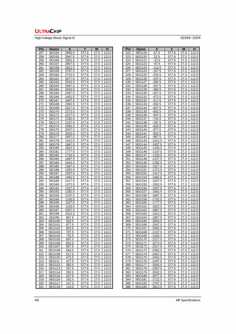
ULTRACHIP
High-Voltage Mixed-Signal IC ©1999~2004
48 MP Specifications
Pin Name X Y W H 257 SEG54 2992.5 577.6 27.0 112.0 258 SEG55 2947.5 577.6 27.0 112.0 259 SEG56 2902.5 577.6 27.0 112.0 260 SEG57 2857.5 577.6 27.0 112.0 261 SEG58 2812.5 577.6 27.0 112.0 262 SEG59 2767.5 577.6 27.0 112.0 263 SEG60 2722.5 577.6 27.0 112.0 264 SEG61 2677.5 577.6 27.0 112.0 265 SEG62 2632.5 577.6 27.0 112.0 266 SEG63 2587.5 577.6 27.0 112.0 267 SEG64 2542.5 577.6 27.0 112.0 268 SEG65 2497.5 577.6 27.0 112.0 269 SEG66 2452.5 577.6 27.0 112.0 270 SEG67 2407.5 577.6 27.0 112.0 271 SEG68 2362.5 577.6 27.0 112.0 272 SEG69 2317.5 577.6 27.0 112.0 273 SEG70 2272.5 577.6 27.0 112.0 274 SEG71 2227.5 577.6 27.0 112.0 275 SEG72 2182.5 577.6 27.0 112.0 276 SEG73 2137.5 577.6 27.0 112.0 277 SEG74 2092.5 577.6 27.0 112.0 278 SEG75 2047.5 577.6 27.0 112.0 279 SEG76 2002.5 577.6 27.0 112.0 280 SEG77 1957.5 577.6 27.0 112.0 281 SEG78 1912.5 577.6 27.0 112.0 282 SEG79 1867.5 577.6 27.0 112.0 283 SEG80 1822.5 577.6 27.0 112.0 284 SEG81 1777.5 577.6 27.0 112.0 285 SEG82 1732.5 577.6 27.0 112.0 286 SEG83 1687.5 577.6 27.0 112.0 287 SEG84 1642.5 577.6 27.0 112.0 288 SEG85 1597.5 577.6 27.0 112.0 289 SEG86 1552.5 577.6 27.0 112.0 290 SEG87 1507.5 577.6 27.0 112.0 291 SEG88 1462.5 577.6 27.0 112.0 292 SEG89 1417.5 577.6 27.0 112.0 293 SEG90 1372.5 577.6 27.0 112.0 294 SEG91 1327.5 577.6 27.0 112.0 295 SEG92 1282.5 577.6 27.0 112.0 296 SEG93 1237.5 577.6 27.0 112.0 297 SEG94 1192.5 577.6 27.0 112.0 298 SEG95 1147.5 577.6 27.0 112.0 299 SEG96 1102.5 577.6 27.0 112.0 300 SEG97 1057.5 577.6 27.0 112.0 301 SEG98 1012.5 577.6 27.0 112.0 302 SEG99 967.5 577.6 27.0 112.0 303 SEG100 922.5 577.6 27.0 112.0 304 SEG101 877.5 577.6 27.0 112.0 305 SEG102 832.5 577.6 27.0 112.0 306 SEG103 787.5 577.6 27.0 112.0 307 SEG104 742.5 577.6 27.0 112.0 308 SEG105 697.5 577.6 27.0 112.0 309 SEG106 652.5 577.6 27.0 112.0 310 SEG107 607.5 577.6 27.0 112.0 311 SEG108 562.5 577.6 27.0 112.0 312 SEG109 517.5 577.6 27.0 112.0 313 SEG110 472.5 577.6 27.0 112.0 314 SEG111 427.5 577.6 27.0 112.0 315 SEG112 382.5 577.6 27.0 112.0 316 SEG113 337.5 577.6 27.0 112.0 317 SEG114 292.5 577.6 27.0 112.0 318 SEG115 247.5 577.6 27.0 112.0 319 SEG116 202.5 577.6 27.0 112.0 320 SEG117 157.5 577.6 27.0 112.0 321 SEG118 112.5 577.6 27.0 112.0
Pin Name X Y W H 322 SEG119 67.5 577.6 27.0 112.0 323 SEG120 22.5 577.6 27.0 112.0 324 SEG121 -22.5 577.6 27.0 112.0 325 SEG122 -67.5 577.6 27.0 112.0 326 SEG123 -112.5 577.6 27.0 112.0 327 SEG124 -157.5 577.6 27.0 112.0 328 SEG125 -202.5 577.6 27.0 112.0 329 SEG126 -247.5 577.6 27.0 112.0 330 SEG127 -292.5 577.6 27.0 112.0 331 SEG128 -337.5 577.6 27.0 112.0 332 SEG129 -382.5 577.6 27.0 112.0 333 SEG130 -427.5 577.6 27.0 112.0 334 SEG131 -472.5 577.6 27.0 112.0 335 SEG132 -517.5 577.6 27.0 112.0 336 SEG133 -562.5 577.6 27.0 112.0 337 SEG134 -607.5 577.6 27.0 112.0 338 SEG135 -652.5 577.6 27.0 112.0 339 SEG136 -697.5 577.6 27.0 112.0 340 SEG137 -742.5 577.6 27.0 112.0 341 SEG138 -787.5 577.6 27.0 112.0 342 SEG139 -832.5 577.6 27.0 112.0 343 SEG140 -877.5 577.6 27.0 112.0 344 SEG141 -922.5 577.6 27.0 112.0 345 SEG142 -967.5 577.6 27.0 112.0 346 SEG143 -1012.5 577.6 27.0 112.0 347 SEG144 -1057.5 577.6 27.0 112.0 348 SEG145 -1102.5 577.6 27.0 112.0 349 SEG146 -1147.5 577.6 27.0 112.0 350 SEG147 -1192.5 577.6 27.0 112.0 351 SEG148 -1237.5 577.6 27.0 112.0 352 SEG149 -1282.5 577.6 27.0 112.0 353 SEG150 -1327.5 577.6 27.0 112.0 354 SEG151 -1372.5 577.6 27.0 112.0 355 SEG152 -1417.5 577.6 27.0 112.0 356 SEG153 -1462.5 577.6 27.0 112.0 357 SEG154 -1507.5 577.6 27.0 112.0 358 SEG155 -1552.5 577.6 27.0 112.0 359 SEG156 -1597.5 577.6 27.0 112.0 360 SEG157 -1642.5 577.6 27.0 112.0 361 SEG158 -1687.5 577.6 27.0 112.0 362 SEG159 -1732.5 577.6 27.0 112.0 363 SEG160 -1777.5 577.6 27.0 112.0 364 SEG161 -1822.5 577.6 27.0 112.0 365 SEG162 -1867.5 577.6 27.0 112.0 366 SEG163 -1912.5 577.6 27.0 112.0 367 SEG164 -1957.5 577.6 27.0 112.0 368 SEG165 -2002.5 577.6 27.0 112.0 369 SEG166 -2047.5 577.6 27.0 112.0 370 SEG167 -2092.5 577.6 27.0 112.0 371 SEG168 -2137.5 577.6 27.0 112.0 372 SEG169 -2182.5 577.6 27.0 112.0 373 SEG170 -2227.5 577.6 27.0 112.0 374 SEG171 -2272.5 577.6 27.0 112.0 375 SEG172 -2317.5 577.6 27.0 112.0 376 SEG173 -2362.5 577.6 27.0 112.0 377 SEG174 -2407.5 577.6 27.0 112.0 378 SEG175 -2452.5 577.6 27.0 112.0 379 SEG176 -2497.5 577.6 27.0 112.0 380 SEG177 -2542.5 577.6 27.0 112.0 381 SEG178 -2587.5 577.6 27.0 112.0 382 SEG179 -2632.5 577.6 27.0 112.0 383 SEG180 -2677.5 577.6 27.0 112.0 384 SEG181 -2722.5 577.6 27.0 112.0 385 SEG182 -2767.5 577.6 27.0 112.0 386 SEG183 -2812.5 577.6 27.0 112.0
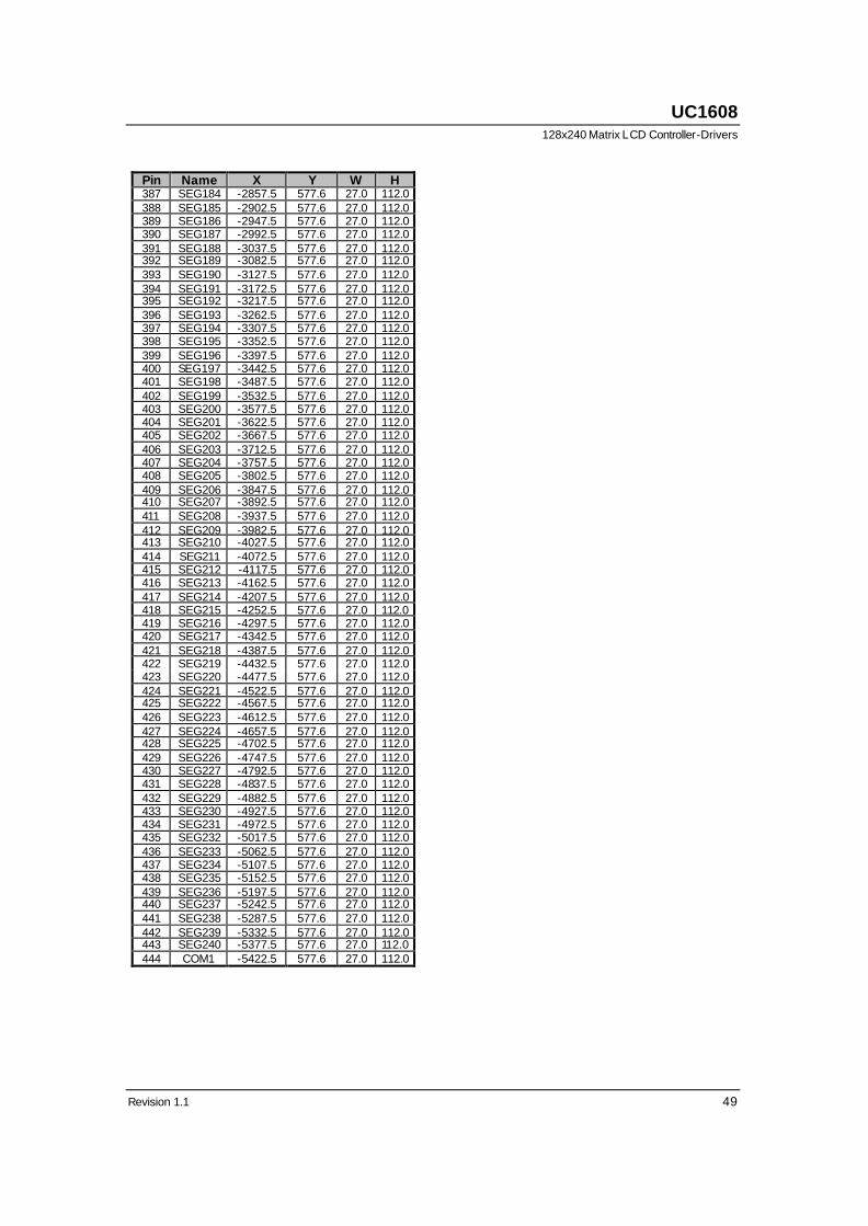
UC1608 128x240 Matrix LCD Controller-Drivers
Revision 1.1 49
Pin Name X Y W H 387 SEG184 -2857.5 577.6 27.0 112.0 388 SEG185 -2902.5 577.6 27.0 112.0 389 SEG186 -2947.5 577.6 27.0 112.0 390 SEG187 -2992.5 577.6 27.0 112.0 391 SEG188 -3037.5 577.6 27.0 112.0 392 SEG189 -3082.5 577.6 27.0 112.0 393 SEG190 -3127.5 577.6 27.0 112.0 394 SEG191 -3172.5 577.6 27.0 112.0 395 SEG192 -3217.5 577.6 27.0 112.0 396 SEG193 -3262.5 577.6 27.0 112.0 397 SEG194 -3307.5 577.6 27.0 112.0 398 SEG195 -3352.5 577.6 27.0 112.0 399 SEG196 -3397.5 577.6 27.0 112.0 400 SEG197 -3442.5 577.6 27.0 112.0 401 SEG198 -3487.5 577.6 27.0 112.0 402 SEG199 -3532.5 577.6 27.0 112.0 403 SEG200 -3577.5 577.6 27.0 112.0 404 SEG201 -3622.5 577.6 27.0 112.0 405 SEG202 -3667.5 577.6 27.0 112.0 406 SEG203 -3712.5 577.6 27.0 112.0 407 SEG204 -3757.5 577.6 27.0 112.0 408 SEG205 -3802.5 577.6 27.0 112.0 409 SEG206 -3847.5 577.6 27.0 112.0 410 SEG207 -3892.5 577.6 27.0 112.0 411 SEG208 -3937.5 577.6 27.0 112.0 412 SEG209 -3982.5 577.6 27.0 112.0 413 SEG210 -4027.5 577.6 27.0 112.0 414 SEG211 -4072.5 577.6 27.0 112.0 415 SEG212 -4117.5 577.6 27.0 112.0 416 SEG213 -4162.5 577.6 27.0 112.0 417 SEG214 -4207.5 577.6 27.0 112.0 418 SEG215 -4252.5 577.6 27.0 112.0 419 SEG216 -4297.5 577.6 27.0 112.0 420 SEG217 -4342.5 577.6 27.0 112.0 421 SEG218 -4387.5 577.6 27.0 112.0 422 SEG219 -4432.5 577.6 27.0 112.0 423 SEG220 -4477.5 577.6 27.0 112.0 424 SEG221 -4522.5 577.6 27.0 112.0 425 SEG222 -4567.5 577.6 27.0 112.0 426 SEG223 -4612.5 577.6 27.0 112.0 427 SEG224 -4657.5 577.6 27.0 112.0 428 SEG225 -4702.5 577.6 27.0 112.0 429 SEG226 -4747.5 577.6 27.0 112.0 430 SEG227 -4792.5 577.6 27.0 112.0 431 SEG228 -4837.5 577.6 27.0 112.0 432 SEG229 -4882.5 577.6 27.0 112.0 433 SEG230 -4927.5 577.6 27.0 112.0 434 SEG231 -4972.5 577.6 27.0 112.0 435 SEG232 -5017.5 577.6 27.0 112.0 436 SEG233 -5062.5 577.6 27.0 112.0 437 SEG234 -5107.5 577.6 27.0 112.0 438 SEG235 -5152.5 577.6 27.0 112.0 439 SEG236 -5197.5 577.6 27.0 112.0 440 SEG237 -5242.5 577.6 27.0 112.0 441 SEG238 -5287.5 577.6 27.0 112.0 442 SEG239 -5332.5 577.6 27.0 112.0 443 SEG240 -5377.5 577.6 27.0 112.0 444 COM1 -5422.5 577.6 27.0 112.0
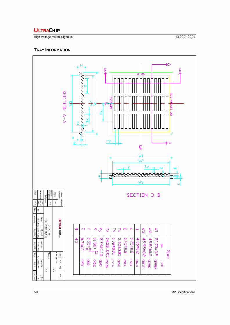
ULTRACHIP
High-Voltage Mixed-Signal IC ©1999~2004
50 MP Specifications
TRAY INFORMATION
Tolerance
Roughness
Dimension
Angle
General
Date04-13-04'
By
Drawn
Jack Chung
Specified
Unless Otherwise
Unit
Rev.
CheckedApproved
1 of 1
Sheet
Size
Drawing No.
Material
Package Code
ScaleN/AProj.
AA4
Type: H20-459×61-28(45)
2" IC Tray
mm
ULT
RAC
HIP
INC.
晶 宏 半 導 體
N/A
N/A
drawing
see
detail
Jack Chung
Leo Peng
04-13-04'
04-13-04'
03-DWG-003-007
N/A
N/A
N/A
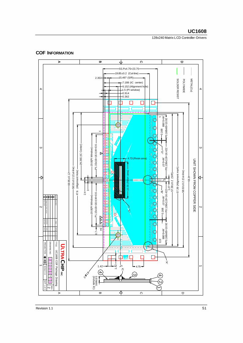
UC1608 128x240 Matrix LCD Controller-Drivers
Revision 1.1 51
COF INFORMATION U
NIT
SH
OW
N F
RO
M C
OP
PE
R S
IDE
SO
LDE
R R
ES
IST
ME
TA
L(Cu)
PO
LYIM
IDE
NC
BM0
BM1
RST
NC
CS
D7
D6
D5
D4
D3
D2
D0
WR1
CD
WR0
D1
VSS
VDD
VLCD
VDD2,3
VB1-
VB1+
VB0-
VB0+
NC
NC
NC
NC
NC
5S.Px4.75=23.7569
.95
±0.1
2
P0.
168x
65=1
0.92
0.16
8
P0.
138x
119=
16.4
22P
0.13
8x11
9=16
.422
P0.
168x
65=1
0.92
0.16
8
57.3
9 (A
lignm
ent m
ark)
58.5
3±0
.2 (
Cut
-line
)
57.3
9±0
.2(S
/R)
7.188 (IC center)
6.152 (Alignment hole)
19.85±0.2 (Cut-line)
15.497 (S/R)
P1.
15x1
6=18
.4,W
=0.6
19.8
(PI W
indo
w)
P1.
15x1
6=18
.4,W
=0.6
19.8
(PI W
indo
w)47
.6(A
lignm
ent H
ole)
1
29.2
65 (
IC C
ente
r)2-
1.8
"A"
"B"
4.751.42
1.42
"D"
4
3
24
1
CLTR
AU
INC.
HIP
,W=0.07
1.27
CL
CL
(Include IC)
58.5
3±0
.2 (C
ut-li
ne)
2.4
0.7
,W=0.07
,W=0.088
,W=0.088
"C"
15.5
6 (R
esin
are
a)
134
1372
4.73 (Resin area)
PR
OJE
CTIO
N
DR
AW
ING
NO
.
UC
1608 CO
F Package D
rawing
SC
ALE
1:1
TIT
LE
UC
61
08
SH
T 1 of 2
FB
RE
V
1 2 3 4 5
Revise
Describtion
DF
TG
.C
HK
.A
PP
VL.
Date
New
version10/07/2003
Jack J.
2
2
A B C D
3
C
1
A B C D
4
B D
2
A
14
3
IC
2.353
0.362
1.5 (PI window)0.914
0.8 MA
X.
66.8
NC
NC
TST4
VBIAS
Change input pin(E
version)06/23/2004
Jacky
22
22
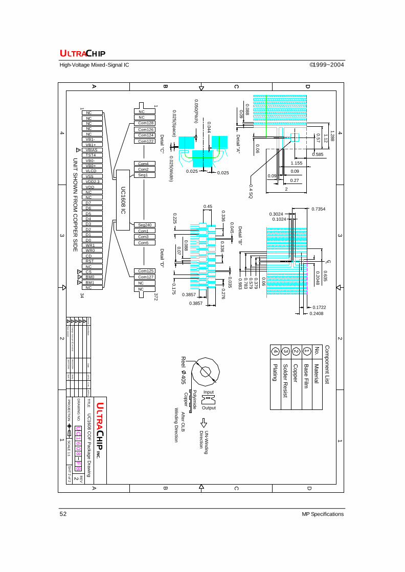
ULTRACHIP
High-Voltage Mixed-Signal IC ©1999~2004
52 MP Specifications
Winding D
irection
Copper
Input
Polyim
ide
UN
-Winding
Direction
Output
Base Film
Copper
Solder R
esist
Plating
234 No.
1
Material
Com
ponent List
Com1
NC
Com5
Com3
Com125
Com127
NC
NC
Com2Com4
Com122
Com124
NC
Com126
Com128
Seg240
Seg1
D2D1D0WR1WR0CDRSTNCCSBM0BM1NC
UC
1608 IC
VBIASTST4VB0-VB0+VLCD
VDD2,3
NCNCNC
VSS
VDDNCNCD7D6D5D4D3
Detail "A
"
22
A B C D
3
C
1
A
4
B C D
4
3P
RO
JEC
TIO
N
DR
AW
ING
NO
.
UC
1608 CO
F P
ackage Draw
ing
SC
ALE
1:1
TITLE
UC
61
08
SH
T 2 of 2
FB
RE
V
A B
CLT
RA
UIN
C.
HIP
1 2 3 4 5
Revise
Describtion
DFTG
.C
HK
.A
PP
VL.
Date
New
version10/07/2003
Jack J.
D
1
Detail "B
"
Detail "C
"D
etail "D"
CL
0.07
0.088
0.06
0.635
0.2048
0.06
0.57
0.45
0.336
0.0450.0350.175
0.225
0.3857
0.2760.336
0.025 0.025
0.044
0.050(Pitch)
0.025(Space)
0.025(Width)
0.9830.7830.5790.379
0.30240.7354
0.1024
0.24080.1722
0.4 SQ
0.090.088
1.2881.12
0.090.27
0.09
1.155
0.585
1372
2
0.3857
134
After O
LB
UN
IT S
HO
WN
FR
OM
CO
PP
ER
SID
E2
NCNCVB1-VB1+
Change input pin (E
version)06/23/2004
Jacky
22
22
Reel
405
UC1608 128x240 Matrix LCD Controller-Drivers
Revision 1.1 53
REVISION HISTORY
Revision Contents Date of Rev.
0.6 Golden Release Jul. 2, 2004
(1) A constraint is added: To keep VDD and VSS under 150 O. (Section “Reference COG Layout”, page 7; Section “ITO Layout Considerations ”, page 21)
(2) Die size was changed to 11480 x 1375. (Section “Revision History” – item 12, page 53)
0.8
(3) The Revision records prior to ES revision are split into a separate file. (Section “Revision History”, page 53)
Jul. 30, 2004
(1) Some texts are marked bold to indicate default. (Section “Control Registers ”, Pp 8~9; “Command Description” – (5) Set Multiplex Rate, page 11; “Command Description” - (19) Set LCD Bias Ratio, page 15)
(2) VDD2/3 is corrected. (Section “LCD Voltage Setting”, page 16)
(3) Note item 1, the recommended CBIAS range is adjusted: 50nF à 0.1µF (Section “VLCD Quick Reference” – Hi-V Reference Circuit, page 19)
1.0
(4) Some AC timings are adjusted. (Section “AC Characteristics ”, Pp 39-40)
Sep. 30, 2004
(1) One more pin is added: VDDX (Section “Pin Description”, page 6)
(2) The COG drawing is updated: VDD à VDDX (Section “COG Reference Layout”, page 7)
(3) Pin 68 is renamed: VDD à VDDX (Section “Pad Coordinates ”, page 46)
(4) In the “Operating Mode” table, the status of Draining Circuit in Sleep mode is corrected: “OFF” à “ON”
(5) Most contents of sub-section “Changing Operation Mode” are re-written.
(Section “Reset & Power Management”, page 33)
(6) Sub-section “Extended Display OFF” is removed. (7) Sub-section “Brief Display OFF” is renamed as “Display OFF”.
(Section “Reset & Power Management”, page 36)
(8) Average Frame Rate, fFR, is adjusted: Max. : 84 à “–“ (dash)
(Section “Specifications” – DC Characteristics, page 38)
1.1
(9) A typo error is corrected: BR=11b à 10b (10) Test Condition (2) is removed.
(Section “Specifications ” – Power Consumption, page 38)
Nov. 4, 2004