Embed Size (px)
Citation preview

Application note
R01AN3496EJ0101 Rev.1.01 Page 1 of 38
Jan. 12, 2017
RL78/G11 UART communication with middle speed on chip oscillator CC-RL
Summary
The application note explains the UART communication method with middle speed on chip oscillator. The middle speed on chip oscillator is periodically measured by high speed on chip oscillator that has the frequency accurate enough requested by the UART communication. UART with the middle speed on chip oscillator communicates by correcting the baud rate of the UART communication based on the result of the measurement.
Object device
RL78/G11
When applying the application note to other microcomputers please change it according to the specification and evaluate it enough.
R01AN3496EJ0101Rev.1.01
Jan. 12, 2017

RL78/G11 UART communication with middle speed on chip oscillator CC-RL
R01AN3496EJ0101 Rev.1.01 Page 2 of 38
Jan. 12, 2017
Contents
1. Specification ............................................................................................................................................. 3
2. Operation condition confirmation ............................................................................................................... 4
3. Related application note ............................................................................................................................. 4
4. Hardware explanation ................................................................................................................................ 5 4.1 Example of hardware structure ........................................................................................................... 5 4.2 Used pin list ...................................................................................................................................... 5
5. Software explanation ................................................................................................................................. 6 5.1 Outline of operation ........................................................................................................................... 6 5.2 Consideration of correction processing ................................................................................................ 8 5.3 Set list of option byte ....................................................................................................................... 10 5.4 Constant list .................................................................................................................................... 10 5.5 Variable list .................................................................................................................................... 11 5.6 Function list .................................................................................................................................... 12 5.7 Function specification ...................................................................................................................... 13 5.8 Flow chart ...................................................................................................................................... 17
5.8.1 Initialization ............................................................................................................................... 17 5.8.2 Peripheral function initialization ................................................................................................ 18 5.8.3 I/O Port Setup ........................................................................................................................... 19 5.8.4 CPU clock initialization ............................................................................................................. 19 5.8.5 Timer array unit initialization ..................................................................................................... 20 5.8.6 8-bit interval timer initialization function .................................................................................... 22 5.8.7 Serial array unit initialization ..................................................................................................... 23 5.8.8 UART0 initialization ................................................................................................................... 24 5.8.9 The main function ..................................................................................................................... 26 5.8.10 The main user initialization ................................................................................................... 28 5.8.11 UART0 reception status initialization .................................................................................... 29 5.8.12 UART0 operation start function ............................................................................................. 30 5.8.13 UART0 data transmission ..................................................................................................... 31 5.8.14 UART0 operation stop .......................................................................................................... 32 5.8.15 UART0 reception completion interrupt .................................................................................. 33 5.8.16 UART0 reception error interrupt ............................................................................................ 34 5.8.17 UART0 transmission complete interrupt ............................................................................... 34 5.8.18 8-bit interval timer interrupt ................................................................................................... 35 5.8.19 TAU channel 3 count complete interrupt .............................................................................. 37
6. Sample code ........................................................................................................................................... 38
7. Reference document ................................................................................................................................ 38

RL78/G11 UART communication with middle speed on chip oscillator CC-RL
R01AN3496EJ0101 Rev.1.01 Page 3 of 38
Jan. 12, 2017
1. Specification
[Explanation of specification]
Table 1.1 shows the used peripheral function and the usage. Figure 1.1 shows the outline of the application.
Table 1.1 Used peripheral function and usage
Function in surrounding Usage
Serial array unit UART communication Timer array unit The division of middle speed on chip oscillator 8-bit interval timer The frequency measurement of middle speed on chip oscillator
MOCO 4MHz …………
Timer array unit 0Channel 1
(N division)
・・・・・・・
Measured waveform4/N MHz
0.25 us
0.25×N us
HOCO 24MHz ・・・・・・・・・・・・・・・
0.04166 us
Timer array unit 0Channel 3
(Input pulse width count)Count
Calculate the radio of count result vs. ideal (theoretical) and overwrite it
onto SDR[15:9]
Figure 1.1 Outline of the application

RL78/G11 UART communication with middle speed on chip oscillator CC-RL
R01AN3496EJ0101 Rev.1.01 Page 4 of 38
Jan. 12, 2017
2. Operation condition confirmation
The sample code of this application note confirms operation at the conditions stated below.
Table 2.1 Operation condition confirmation
Item Content
MCU RL78/G11 (R5F1056A) Operating frequency ・Middle speed on chip oscillator clock (fIM): 4MHz (at UART communication).
・High speed on chip oscillator clock (fIH): 24MHz (at MOCO frequency measurement).
Operation voltage 3.3 V (Able to operate at 1.6V-3.6V). LVD operation (VLVD): Reset mode 2.81V (2.76V to 2.87V)
Integrated development environment(CS+)
CS+ for CC V4.01.00 from Renesas Electronics Corp.
C compiler(CS+) CC-RL V1.02.00 from Renesas Electronics Corp. Integrated development environment(e2studio)
e2studio V5.2.0.020 from Renesas Electronics Corp.
C compiler(e2studio) CC-RL V1.02.00 from Renesas Electronics Corp.
3. Related application note
The application note that relates to this application note is shown below.
RL78/G13 initialization (R01AN2575EJ)
RL78/G13 serial array unit (UART communication) (R01AN2517EJ)

RL78/G11 UART communication with middle speed on chip oscillator CC-RL
R01AN3496EJ0101 Rev.1.01 Page 5 of 38
Jan. 12, 2017
4. Hardware explanation
4.1 Example of hardware structure Figure 4.1 shows the connection example.
RL78/G11
VSS
VDD
P40/TOOL0 For on chip debug
RESET
P01
REGC
LED1
P30/TO01
P00/TI03
P54/TxD0
P55/RxD0Conmunication device
Figure 4.1 Connection example
Note: 1. It is the circuit image and shows the simplified outline of the connection. Please design to do the pin processing etc. appropriately, and to meet with the electrical characteristics when the circuit is actually designed (Please connect the input only port to VDD or VSS through a resistor individually).
2 Please connect it with VDD if there the pin name starts by EVDD, and to VSS if the pin name starts by EVSS respectively.
3 Please make the VDD more than reset release voltage (VLVD) set in LVD.
4.2 Used pin list Table 4.1 shows the used pin and function.
Table 4.1 Used pin and function
Pin name I/O Content
P01 Output LED turning on P30/TO01 Output MOCO division waveform output P00/TI03 Input Frequency measuring waveform input

RL78/G11 UART communication with middle speed on chip oscillator CC-RL
R01AN3496EJ0101 Rev.1.01 Page 6 of 38
Jan. 12, 2017
5. Software explanation
5.1 Outline of operation In this sample code, data corresponding to the data received from another device is transmitted back to the device.
When the error occurs, data corresponding to the error is transmitted to the device. Table 5.1 and Table 5.2 show correspondence tables of receive data and the transmission data, error detection respectively.
Table 5.1 Correspondence of receive data and transmission data
Receive data Response (transmission) data
T(54H) O(4FH), K(4BH), "CR"(0DH), "LF"(0AH)
t(74H) o(6FH), k(6BH), "CR"(0DH), "LF"(0AH)
Others U(55H), C(43H), "CR"(0DH), "LF"(0AH)
Table 5.2 Correspondence of transmission data when error is detected
Occurred error Response (transmission) data
Parity error P(50H), E(45H), "CR"(0DH), "LF"(0AH)
Flaming error F(46H), E(45H), "CR"(0DH), "LF"(0AH)
Overrunning error O(4FH), E(45H), "CR"(0DH), "LF"(0AH)
(1) UART is initialized.
< UART setting condition >
SAU0 channels 0 and 1 are used as UART.
P54/TxD0 is used for data output pin P55/RxD0 is used for data input pin.
The data length uses 8-bit.
Data transfer.direction.setting.is LSB first.
The parity setting uses the even parity.
Receive data and the level setting use the standard.
Transfer rate uses 9600bps.
Reception complete interrupt (INTSR0), transmission complete interrupt (INTST0), and error interrupt (INTSRE0) are used.
The interrupt priority level of INTSR0, INTST0, and INTSRE0 uses the low priority (level 3).
(2) 8-bit interval timer is initialized.
< 8-bit interval timer setting condition >
The interrupt priority level of 8-bit interval timer interrupt (INTIT00) uses the low priority (level 3).
It uses it in 8-bit count mode.
One division frequency is set to fail/64.
The compare value is set to 0xE9 so that INTIT00 is generated around every second.

RL78/G11 UART communication with middle speed on chip oscillator CC-RL
R01AN3496EJ0101 Rev.1.01 Page 7 of 38
Jan. 12, 2017
(3)The timer array unit is initialized.
< Channel 1 setting condition >
The operation clock is middle speed on chip oscillator (MOCO) 4MHz.
It operates as 16-bit timers.
It sets software trigger start
MOCO effective edge is falling edge
It operates as interval timer mode/square waveform output.
The timer interrupt is not generated at the start of counting.
Positive logic output
< Channel 3 setting condition >
The operation clock is high speed on chip oscillator (HOCO) 24MHz.
It sets single channel operation
An effective edge of the pin TI03 is set as start trigger and a capture trigger.
Effective edge of pin TI03: Rising edge
It operates as input pulse width measurement mode.
Positive logic output
(4) After setting communication standby state in the serial channel start register, the HALT instruction is executed. The process is triggered by the reception complete interrupt (INTSR0) and error interrupt (INTSRE0).
When INTSR0 is generated, data is received, and data corresponding to the receive data is transmitted. When INTSRE0 is generated, it processes the error and transmits the data corresponding to the error. 8-bit interval timer stops in the period of transmission response processing. After data reception, the HALT instruction is executed again, and it waits for reception complete interrupt (INTSR0), error interrupt (INTSRE0).
In the case of any factors, that doesn't relates to 8-bit interval interrupt and timer interrupt but wake up MCU from HALT to normal operation, it goes back to HALT without any processing.
(5) The baud rate is corrected by 8-bit interval timer interrupt.
LED that shows the baud rate correction processing is turned on.
UART0 stops operation.
Operation HOCO and wait for oscillation stabilization time.
CPU clock source is switched from MOCO to HOCO.
TAU0 channel 1 and channel 3 start to operate. It stands by in HALT state until the 2nd time channel 3 complete interrupt generation.
After the 2nd time channel 3 complete interrupt generation, TAU0, channel 1, and channel 3 stop operation.
It counts backward from the result of a measurement, and the baud rate correction value is written into the SDR register.
CPU clock is switched back from HOCO (24MHz) to MOCO (4MHz) in preparation for the UART communication.
HOCO oscillation is stopped.
UART0 starts operation.
LED that shows the baud rate correction processing is turned off.

RL78/G11 UART communication with middle speed on chip oscillator CC-RL
R01AN3496EJ0101 Rev.1.01 Page 8 of 38
Jan. 12, 2017
5.2 Consideration of correction processing The following explains the detail of the correction processing method.
(1) The generation of object waveform to be measured
As shown in Figure 1.1, the middle speed on chip oscillator (MOCO) is divided in N and generates the object waveform to be measured. Enlarging the value of N as much as possible makes the measurement more accurate. In other hand, it should be within the 16-bit range for timer array unit 0 channels 3 to count. Based on HOCO to be 24MHz±1% and MOCO to be 4MHz±12% , Table 5.3 shows the measurement (count) result in the combination of each Max., Typ. and Min. value.
Table 5.3 The result of measurement for the waveform N divided from MOCO.
MOCO (4 MHz±12%)
Min.: 3.52 MHz Typ.: 4.00 MHz Max.: 4.42 MHz
HOCO
(24 MHz±1%)
Max: 24.24 MHz (24.24 / 3.52) N = 6.886N
(24.24 / 4.00) N = 6.060N
(24.24 / 4.42) N = 5.484N
Typ.: 24.00 MHz (24.00 / 3.52) N = 6.818N
(24.00 / 4.00) N = 6.000N
(24.00 / 4.42) N = 5.430N
Min.: 23.76 MHz (23.76 / 3.52) N = 6.750N
(23.76 / 4.00) N = 5.940N
(23.76 / 4.42) N = 5.376N
As shown in Table 5.3, in the case of MOCO is 3.52MHz and HOCO is 24.24MHz, the count value of the measurement result goes to the most. Therefore, N can be calculated by the following expressions.
(24.24 / 3.52) N < 2^16 -1
N < 65535 * 3.52 / 24.24
N < 9516.6
∴ N (Max) = 9516
Here, the TDR01 register sets the half cycle of the object waveform to be measured. Therefore, the set value is as follows. Please confirm the r_it8bit0_channel0_interrupt function.
Value set to TDR01 = N/2-1
= 4757 (0x1295)
RL78/G11 UART communication with middle speed on chip oscillator CC-RL
R01AN3496EJ0101 Rev.1.01 Page 9 of 38
Jan. 12, 2017
(2) Baud rate correction
UART of this application sets MOCO driven as fCLK = 4MHz and fMCK = CK00= fCLK/ 2= 2MHz. Because the target baud rate is 9600bps, the SDR [15:9] value for upper 7 bits of SDR register is calculated by the following expression.
SDR[15:9] + 1 = fMCK / (2 * 9600)
= 2 MHz / (2 * 9600)
In addition, considering the frequency accuracy of MOCO, the expression is as follows.
SDR 15:9 + 1 = 2 MHz * (ideal count value/ capture value of CH3) / (2 * 9600)
= 2 MHz * (6.000* N/ capture value of CH3) / (2 * 9600)
= 2 MHz * (6 * 9516/ capture value of CH3) / (2 * 9600)
= 5947500/ (capture value of CH3)
To simplify the calculation, the right denominator and the molecule are divided respectively by 256(= 2^8), the final expression is as follows. In this sample program, it is described by the r it8bit0_channel0_interrupt function. Please confirm that the left side value SDR[15:9].is described as local variable k.
= 23232/ (eight high rank bits of capture value of CH3)

RL78/G11 UART communication with middle speed on chip oscillator CC-RL
R01AN3496EJ0101 Rev.1.01 Page 10 of 38
Jan. 12, 2017
5.3 Set list of option byte Table 5.4 shows the optional byte setting.
Table 5.4 Optional byte setting
Address Set value Content
000C0H/010C0H 1110 1111B Watch dog timer operation prohibition (count stop after reset)
000C1H/010C1H 0111 1111B LVD reset mode, 2.81V(2.76 to 2.87V) 000C2H/010C2H 1110 0000B HS mode, HOCO:24MHz 000C3H/010C3H 1000 0100B Enables the on-chip debugging
5.4 Constant list Table 5.5 shows the constant used by the sample code.
Table 5.5 Constant used by sample code
Constant name Set value Content
MessageOK[4] "OK¥r¥n" Return message when “T" is received Messageok[4] "ok¥r¥n" Return message when “t" is received MessageUC[4] "UC¥r¥n" Return message when receiving other than “T" or "t" MessageFE[4] "FE¥r¥n" Return message at flaming error MessagePE[4] "PE¥r¥n" Return message at parity error MessageOE[4] "OE¥r¥n" Return message at overrun error

RL78/G11 UART communication with middle speed on chip oscillator CC-RL
R01AN3496EJ0101 Rev.1.01 Page 11 of 38
Jan. 12, 2017
5.5 Variable list Table 5.6 shows the global variable.
Table 5.6 Global variable
Type Variable identifier Content Used function
uint8_t g_uart0_rx_buf Receive data buffer main uint8_t* gp_uart0_tx_address Transmission data pointer R_UART0_Send、
R_uart0_interrupt_send uint16_t g_uart0_tx_count Transmission data number counter R_UART0_Send、
r_uart0_interrupt_send uint8_t* gp_uart0_rx_address Receive data pointer
R_UART0_Receive、r_uart0_interrupt_receive、r_uart0_interrupt_error
uint16_t g_uart0_rx_count Receive data number counter R_UART0_Receive、r_uart0_interrupt_receive
uint16_t g_uart0_rx_length Receive data number R_UART0_Receive、r_uart0_interrupt_receive
uint8_t g_valid_measure Interrupt generation times of TAU0 channel 3
r_it8bit0_channel0_interrupt r_tau0_channel3_interrupt
MDSTATUS g_uart0_tx_end UART transmission processing complete flag
main
uint8_t g_uart0_after_adjustment Flag immediately after passage of 8-bit interval timer interrupt function
main r_it8bit0_channel0_interrupt
uint32_t g_tau0_ch3_width Result of a measurement at one square wave cycle
r_tau0_channel3_interrupt r_it8bit0_channel0_interrupt
uint8_t g_uart0_rx_err UART communication status main r_uart0_callback_receiveend r_uart0_callback_error

RL78/G11 UART communication with middle speed on chip oscillator CC-RL
R01AN3496EJ0101 Rev.1.01 Page 12 of 38
Jan. 12, 2017
5.6 Function list Table 5.7 shows the function list.
Table 5.7 Function list
Function name Outline
main The main function R_MAIN_UserInit The main user initialization function R_UART0_Receive UART0 reception status initialization function R_UART0_Start UART0 operation start function R_UART0_Send UART0 data transmission function R_UART0_Stop UART0 operation stop function r_uart0_interrupt_receive UART0 reception complete interrupt function r_uart0_interrupt_error UART0 reception error interrupt function r_uart0_interrupt_send UART0 transmission complete interrupt function r_it8bit0_channel0_interrupt 8-bit interval timer interrupt function r_tau0_channel3_interrupt TAU Channel 3 count complete interrupt function R_TAU0_Channel1_Start TAU Channel 1 operation start function R_TAU0_Channel3_Start TAU Channel 3 operation start function R_TAU0_Channel1_Stop TAU Channel 1 operation stop function R_TAU0_Channel3_Stop TAU Channel 3 operation stop function R_IT8Bit0_Channel0_Start 8-bit interval timer operation start function R_IT8Bit0_Channel0_Stop 8-bit interval timer operation stop function

RL78/G11 UART communication with middle speed on chip oscillator CC-RL
R01AN3496EJ0101 Rev.1.01 Page 13 of 38
Jan. 12, 2017
5.7 Function specification The following shows the sample code function specification.
Function name Main
Outline The main function Header r_cg_macrodriver.h、r_cg_cgc.h、r_cg_port.h、r_cg_tau.h、r_cg_it8bit.h、r_cg_sau.h
Declaration - Explanation After the main user initialization function is executed, MCU enters HALT state and waits the
UART reception interrupt. When the UART reception complete interrupt is generated, UART transmission is processed for response. When the factor for the HALT release is not UART reception, UART transmission will not be processed and MCU returns to HALT state again.
Parameter None Return value None
Function name R_MAIN_UserInit
Outline The main user initialization function Header r_cg_macrodriver.h、r_cg_cgc.h、r_cg_port.h、r_cg_tau.h、r_cg_it8bit.h、r_cg_sau.h
Declaration void R_MAIN_UserInit(void); Explanation After UART0 and LED are initialized, enable the UART0 and 8-bit interval timer operation.
at last, enable interrupt by the EI instruction. Parameter None
Return value None
Function name R_UART0_Receive
Outline UART0 reception status initialization function Header r_cg_macrodriver.h、r_cg_sau.h
Declaration MD_STATUS R_UART0_Receive(uint8_t * const rx_buf, uint16_t rx_num); Explanation Set the UART0 reception status. Parameter uint8_t* const rx_buf
uint16_t rx_num :Address in receive data buffer :Size of receive data buffer
Return value For MD_OK: The reception setting completion. For MD_ARGERROR: The reception setting failure.
Function name R_UART0_Start
Outline UART0 operation start function Header r_cg_macrodriver.h、r_cg_sau.h
Declaration void R_UART0_Start(void); Explanation Enable serial array unit channel 0, 1 operation. Let UART in communication standby state.. Parameter None
Return value None

RL78/G11 UART communication with middle speed on chip oscillator CC-RL
R01AN3496EJ0101 Rev.1.01 Page 14 of 38
Jan. 12, 2017
Function name R_UART0_Send
Outline UART0 data transmission function Header r_cg_macrodriver.h、r_cg_sau.h
Declaration MD_STATUS R_UART0_Send(uint8_t * const tx_buf, uint16_t tx_num); Explanation Initialize the UART0 transmission starts the data transmission. Parameter uint8_t* const tx_buf
uint16_t tx_num :Address in transmission data buffer :Size of transmission data buffer
Return value For MD_OK: The transmission setting completion. For MD_ARGERROR: The transmission setting failure.
Function name R_UART0_Stop
Outline UART0 operation stop function Header r_cg_macrodriver.h、r_cg_sau.h
Declaration void R_UART0_Stop(void); Explanation Stop serial array 0 unit 0 channel 0, 1 operation. Stop UART communication. Parameter None
Return value None
Function name R_uart0_interrupt_receive
Outline UART0 reception complete interrupt function Header r_cg_macrodriver.h、r_cg_sau.h
Declaration static void __near r_uart0_interrupt_receive(void) Explanation The received data is stored in RAM, and the address and the reception times values are
updated. Parameter None
Return value None
Function name R_uart0_interrupt_error
Outline UART0 reception error interrupt function Header r_cg_macrodriver.h、r_cg_sau.h
Declaration static void __near r_uart0_interrupt_error(void) Explanation Store the reception data in RAM Response the corresponding data by the detected error from
the r_uart0_callback_error function. Parameter None
Return value None
Function name R_uart0_interrupt_send
Outline UART0 transmission complete interrupt function Header r_cg_macrodriver.h、r_cg_sau.h
Declaration static void __near r_uart0_interrupt_send(void) Explanation Transmit the data update the pointer and the counter. In the case of transmission data doesn't
remain, process the transmission completion. Parameter None
Return value None

RL78/G11 UART communication with middle speed on chip oscillator CC-RL
R01AN3496EJ0101 Rev.1.01 Page 15 of 38
Jan. 12, 2017
Function name R_it8bit0_interrupt
Outline 8-bit interval timer interrupt function Header r_cg_macrodriver.h、r_cg_it8bit.h、r_cg_sau.h、r_cg_tau.h
Declaration static void __near r_it8bit0_channel0_interrupt(void) Explanation The function that executes the baud rate correction periodically (It is every 1 second in this
application). Disable the UART communication first. Start timer array unit 0 channel 1 and channel 3. Channel 3 measures the pulse width of object square waveform generated from channel 1. Calculate the result backward and modify the clock division to make it as close to the ideal value as possible. After that, enable the UART communication and return to the UART communication standby state again.
Parameter None Return value None
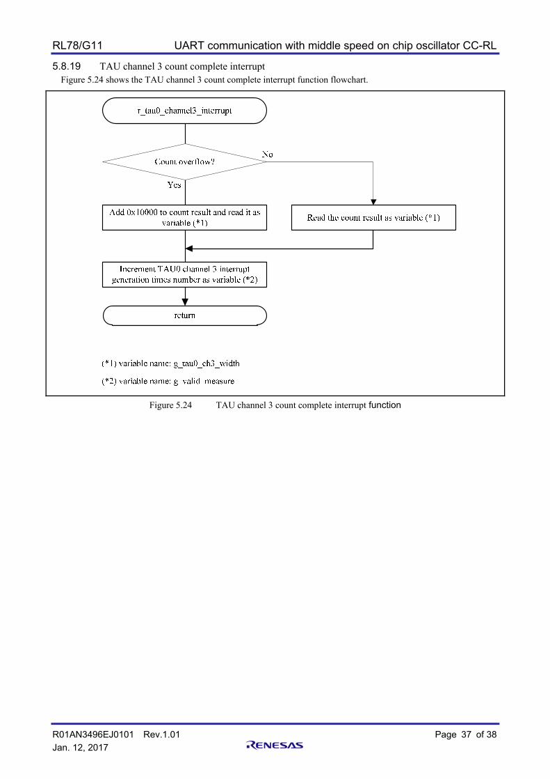
Function name R_tau0_channel3_interrupt
Outline TAU channel 3 count complete interrupt function Header r_cg_macrodriver.h、r_cg_tau.h
Declaration static void __near r_tau0_channel3_interrupt(void) Explanation Store the result of the pulse width measured by the timer array unit channel 3 in the global
variable. Parameter None
Return value None
Function name R_TAU0_Channel1_Start
Outline TAU Channel 1 operation start function Header r_cg_macrodriver.h、r_cg_tau.h
Declaration void R_TAU0_Channel1_Start(void); Explanation Enable timer array unit channel 1 operation. Start a square wave output. Parameter None
Return value None
Function name R_TAU0_Channel3_Start
Outline TAU Channel 3 operation start function Header r_cg_macrodriver.h、r_cg_tau.h
Declaration void R_TAU0_Channel3_Start(void); Explanation Enable timer array unit channel 1 operation. Start the pulse width measurement. Parameter None
Return value None
Function name R_TAU0_Channel1_Stop
Outline TAU Channel 1 operation stop function Header r_cg_macrodriver.h、r_cg_tau.h
Declaration void R_TAU0_Channel1_Stop(void); Explanation Stop timer array unit channel 1. Parameter None
Return value None

RL78/G11 UART communication with middle speed on chip oscillator CC-RL
R01AN3496EJ0101 Rev.1.01 Page 16 of 38
Jan. 12, 2017
Function name R_TAU0_Channel3_Stop
Outline TAU Channel 3 operation stop function Header r_cg_macrodriver.h、r_cg_tau.h
Declaration void R_TAU0_Channel3_Stop(void); Explanation Stop timer array unit channel 3. Parameter None
Return value None
Function name R_IT8Bit0_Channel0_Start
Outline 8-bit interval timer operation start function Header r_cg_macrodriver.h、r_cg_it8bit.h
Declaration void R_IT8Bit0_Channel0_Start(void); Explanation Enable 8-bit interval timer operation. Parameter None
Return value None
Function name R_IT8Bit0_Channel0_Stop
Outline 8-bit interval timer operation stop function Header r_cg_macrodriver.h、r_cg_it8bit.h
Declaration void R_IT8Bit0_Channel0_Stop(void); Explanation Stop 8-bit interval timer. Parameter None
Return value None
RL78/G11 UART communication with middle speed on chip oscillator CC-RL
R01AN3496EJ0101 Rev.1.01 Page 17 of 38
Jan. 12, 2017
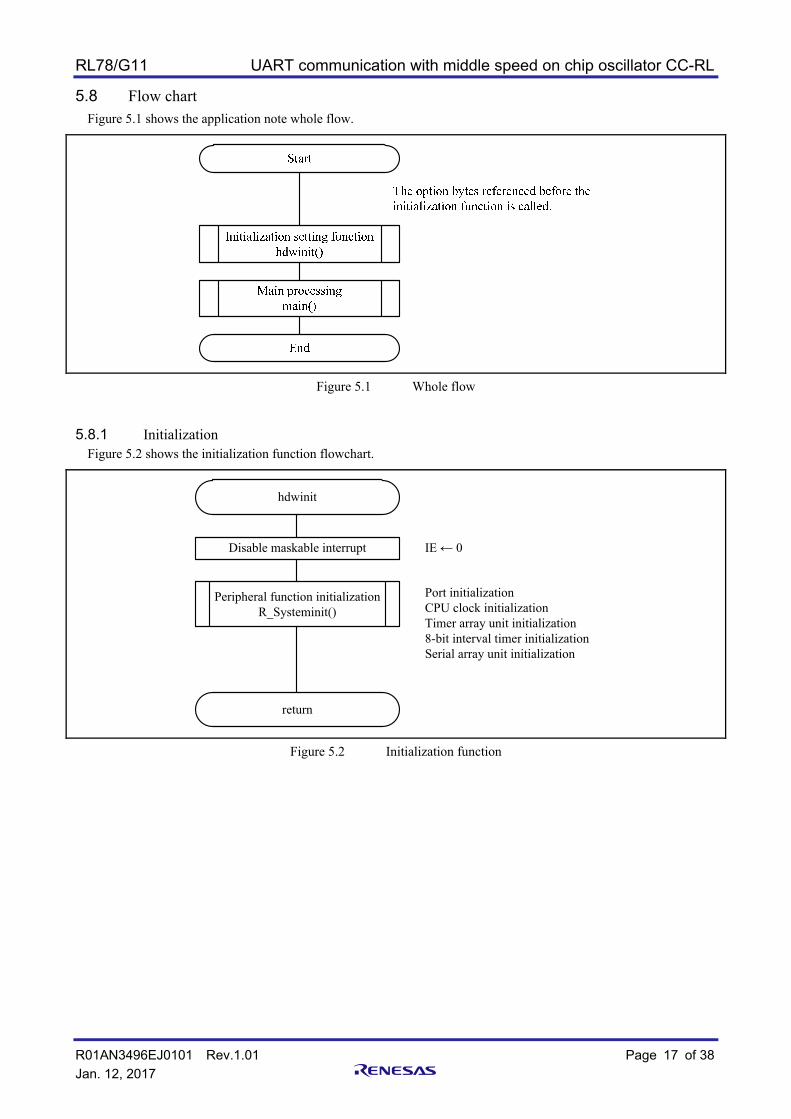
5.8 Flow chart Figure 5.1 shows the application note whole flow.
Figure 5.1 Whole flow
5.8.1 Initialization Figure 5.2 shows the initialization function flowchart.
hdwinit
Disable maskable interrupt
Peripheral function initializationR_Systeminit()
return
IE ← 0
Port initializationCPU clock initializationTimer array unit initialization8-bit interval timer initializationSerial array unit initialization
Figure 5.2 Initialization function

RL78/G11 UART communication with middle speed on chip oscillator CC-RL
R01AN3496EJ0101 Rev.1.01 Page 18 of 38
Jan. 12, 2017
5.8.2 Peripheral function initialization Figure 5.3 shows the peripheral function initialization flowchart.
R_Systeminit
Peripheral I/O redirectionFunction disable
PIOR0 register 00HPIOR1 register 00HPIOR2 register 00HPIOR3 register 00H
CPU clock initializationR_CGC_Create()
8-bit interval timerinitialization
R_IT8Bit0_Channel0_Create()
return
Input/ Output settingR_PORT_Create()
Timer array unitinitialization
R_TAU0_Create()
Serial array unitinitialization
R_SAU0_Create()
Disabled the invalid memoryaccess detection
IAWCTL register 00H
Figure 5.3 Peripheral function initialization function
RL78/G11 UART communication with middle speed on chip oscillator CC-RL
R01AN3496EJ0101 Rev.1.01 Page 19 of 38
Jan. 12, 2017
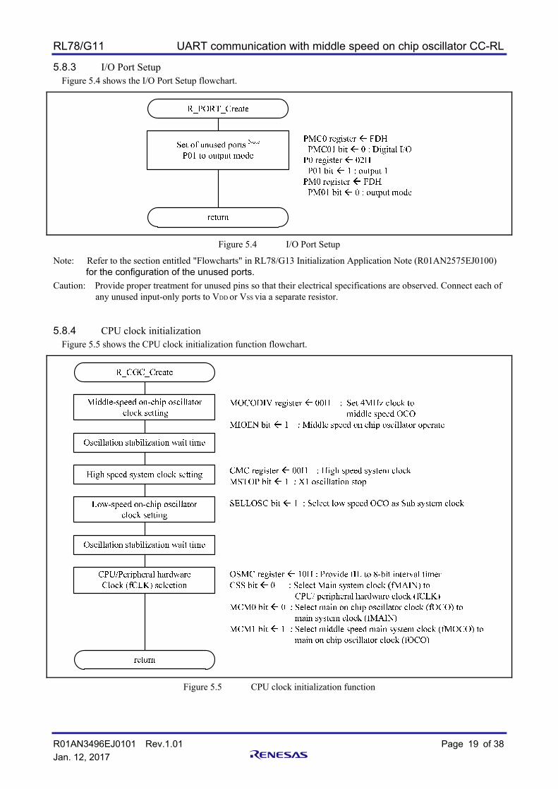
5.8.3 I/O Port Setup Figure 5.4 shows the I/O Port Setup flowchart.
Figure 5.4 I/O Port Setup
Note: Refer to the section entitled "Flowcharts" in RL78/G13 Initialization Application Note (R01AN2575EJ0100) for the configuration of the unused ports.
Caution: Provide proper treatment for unused pins so that their electrical specifications are observed. Connect each of any unused input-only ports to VDD or VSS via a separate resistor.
5.8.4 CPU clock initialization Figure 5.5 shows the CPU clock initialization function flowchart.
Figure 5.5 CPU clock initialization function

RL78/G11 UART communication with middle speed on chip oscillator CC-RL
R01AN3496EJ0101 Rev.1.01 Page 20 of 38
Jan. 12, 2017
5.8.5 Timer array unit initialization Figure 5.6, Figure 5.7 shows the timer array unit initialization flowchart.
Figure 5.6 Timer array unit initialization(1/2)

RL78/G11 UART communication with middle speed on chip oscillator CC-RL
R01AN3496EJ0101 Rev.1.01 Page 21 of 38
Jan. 12, 2017
return
Set TO01 pin, TI03 pinas alternate ports
Channel 1 initialization (square waveform generation)- Operation clock: CK00 (24MHz)(tentative setting)- Operate as 16-bit timer- Software trigger start- Select the operation clock CK00- Interval timer mode- No timer interrupt generated at count start- Channel 1: Master channel output mode- Channel 1: Positive logic output- Set channel 1 output to 0- Channel 1 output enable
TMR01 register 0000HTDR01 register 1295HTOM0 register bit 0TOL0 register bit 1 0TO0 register bit 1 0TOE0 register bit 1 1
Channel 3 initialization(input pulse measurement)- Operation clock: CK00 (24MHz)- Independent channel operation
- Set TI03 pin effective edge as start trigger, capture trigger
- TI03 pin effective edge: Rising edge- Input pulse width measurement mode- No timer interrupt generated at count start- Channel 3: Master channel output mode- Channel 3: Positive logic output- Set channel 3 output to 0- Channel 3 output enable
TMR03 register 0144HTOM0 register bit 3 0TOL0 register bit 3 0TO0 register bit 3 0TOE0 register bit 3 0
TI03 pin noise filter disable NFEN1 register bit 3 0
1
POM3.0 bit 0PMC3.0 bit 0P3.0 bit 0PM3.0 bit 0PCM0.0 bit 0PM0.0 bit 1
Figure 5.7 Timer array unit initialization(2/2)

RL78/G11 UART communication with middle speed on chip oscillator CC-RL
R01AN3496EJ0101 Rev.1.01 Page 22 of 38
Jan. 12, 2017
5.8.6 8-bit interval timer initialization function Figure 5.8 shows the 8-bit interval timer initialization function flowchart.
Figure 5.8 8-bit interval timer initialization function

RL78/G11 UART communication with middle speed on chip oscillator CC-RL
R01AN3496EJ0101 Rev.1.01 Page 23 of 38
Jan. 12, 2017
5.8.7 Serial array unit initialization Figure 5.9 shows the serial array unit initialization function flowchart.
Figure 5.9 Serial array unit initialization function

RL78/G11 UART communication with middle speed on chip oscillator CC-RL
R01AN3496EJ0101 Rev.1.01 Page 24 of 38
Jan. 12, 2017
5.8.8 UART0 initialization Figure 5.10, Figure 5.11 shows UART0 initialization flowchart.
R_UART0_Create
Channel array unit rest ST0 register 0003H
UART reception interrupt complete interrupt (INTSR0) disable, interrupt request flag clear
SRMK0 bit 1SRIF0 bit 0
UART transmission complete interrupt (INTST0) disable, interrupt request flag clear
STMK0 bit 1STIF0 bit 0
UART reception error interrupt (INTSRE0) disable, interrupt request flag clear
SREMK0 bit 1SREIF0 bit 0
Set interrupt priority levelINTSR0: Level 3 (lowest level)
INTSRE0: Level 3 (lowest level)INTST0: Level 3 (lowest level)
SRPR10 bit 1SRPR00 bit 1SREPR10 bit 1SREPR00 bit 1
STPR10 bit 1STPR00 bit 1
Channel 0 (UART transmission) initialization- Set operation clock to CK00- Set transfer clock to CK00 division clock (2 division)- UART mode- Set interrupt factor to transfer complete interrupt
- Transmission only- Error interrupt disable- Even parity- LSB first- Stop bit =1 bit- 8-bit data length
- Noise filter enable
SMR00 register 0022HSCR00 register 8297HSDR00 register CE00HNFEN0 register.bit0 1
1
Figure 5.10 UART0 initialization(1/2)

RL78/G11 UART communication with middle speed on chip oscillator CC-RL
R01AN3496EJ0101 Rev.1.01 Page 25 of 38
Jan. 12, 2017
return
Set channel 0 serial output default value to 1 SO0 register bit 0 1
Channel 1 (UART reception) initialization- Clear all error flags
- Set operation clock to CK00- Set transfer clock toCK00 division clock (2 division)- Set start trigger to RxD0 pin effective edge- Set start bit detection to falling edge- UART mode- Set interrupt source to transfer complete interrupt
- Reception only- Error interrupt generation enable- Even parity- LSB first- Stop bit =1 bit- 8-bit data length
SIR01 register ← 0007HSMR01 register ← 0122HSCR01 register ← 4697HSDR01 register ← CE00H
Set channel 0 output to non-reversed SOL0 register bit 0 0
Set channel 0 serial output enable SOE0 register bit 0 1
RxD0 pin initialization PM5 register bit 5 1
TxD0 pin initialization P5.4 bit 1PM5.4 bit 0
1
Figure 5.11 UART0 initialization(2/2)

RL78/G11 UART communication with middle speed on chip oscillator CC-RL
R01AN3496EJ0101 Rev.1.01 Page 26 of 38
Jan. 12, 2017
5.8.9 The main function Figure 5.12 and Figure 5.13 show main function flowcharts.
Figure 5.12 Main function (1/2)

RL78/G11 UART communication with middle speed on chip oscillator CC-RL
R01AN3496EJ0101 Rev.1.01 Page 27 of 38
Jan. 12, 2017
1
What is the reception data?
UART0 data transmission functionR_UART0_Send()
UART0 data transmission functionR_UART0_Send()
UART0 data transmission functionR_UART0_Send()
= “T”= “t”
=other than “T”, “t”
Transmission complete?
Parameter: “OK”
Parameter: “ok”
Parameter: “UC”
NoYes2
Reception interrupt enableSRMK0 bit 0SREMK0 bit 0
8-bit interval timer operation enableR_IT8Bit0_Channel0_Sart()
UART0 reception status initialized functionR_UART0_Receive()
3
Overrun error?
Yes
Transmission complete?
YesNo
UART0 data transmission functionR_UART0_Send()
Parameter: “OE”
No
Figure 5.13 Main processing (2/2)

RL78/G11 UART communication with middle speed on chip oscillator CC-RL
R01AN3496EJ0101 Rev.1.01 Page 28 of 38
Jan. 12, 2017
5.8.10 The main user initialization Figure 5.14 shows the main user initialization function flowchart.
Figure 5.14 Main user initialization function

RL78/G11 UART communication with middle speed on chip oscillator CC-RL
R01AN3496EJ0101 Rev.1.01 Page 29 of 38
Jan. 12, 2017
5.8.11 UART0 reception status initialization Figure 5.15 shows the UART0 reception status initialization function flowchart.
R_UART0_Receive
Set OK to status default value
return
Set MD_ARGERROR to status
Data number under 1?
Yes
No
Set return value to status
Initialize reception data number count value to 0
Set global variable to reception data number
Initialize reception data pointer
Figure 5.15 UART0 reception status initialization function

RL78/G11 UART communication with middle speed on chip oscillator CC-RL
R01AN3496EJ0101 Rev.1.01 Page 30 of 38
Jan. 12, 2017
5.8.12 UART0 operation start function Figure 5.16 shows UART0 operation start function flowchart.
Figure 5.16 UART0 operation start function

RL78/G11 UART communication with middle speed on chip oscillator CC-RL
R01AN3496EJ0101 Rev.1.01 Page 31 of 38
Jan. 12, 2017
5.8.13 UART0 data transmission Figure 5.17 shows the UART0 data transmission function flowchart.
Figure 5.17 UART0 data transmission function

RL78/G11 UART communication with middle speed on chip oscillator CC-RL
R01AN3496EJ0101 Rev.1.01 Page 32 of 38
Jan. 12, 2017
5.8.14 UART0 operation stop Figure 5.18 shows the UART0 operation stop function flowchart.
R_UART0_Stop
Disable transmission interrupt STMK0 bit 1
return
Disable reception interruptSRMK0 bit 1SREMK0 bit 1
Disable UART0 output SOE0 register bit 0 0
Stop UART0 operation ST0 register bit 0 1ST0 register bit 1 1
Clear transmission interrupt flag STIF0 bit 0
Clear reception interrupt flagSRIF0 bit 0SREIF0 bit 0
Figure 5.18 UART0 operation stop function

RL78/G11 UART communication with middle speed on chip oscillator CC-RL
R01AN3496EJ0101 Rev.1.01 Page 33 of 38
Jan. 12, 2017
5.8.15 UART0 reception completion interrupt Figure 5.19 shows the UART0 reception complete interrupt function flowchart.
r_uart0_interrupt_receive
Store reception data
return
Update the pointer and count
Within the setting data number?
UART0 reception data number over processing function
r_uart0_callback_softwareoverrun()
Yes
No
Read reception data as variable
Reach the setting data number?
Yes
No
UART0 reception data classify functionr_uart0_callback_reiveend()
g_uart0_rx_err 0
Variable: rx_data
Figure 5.19 UART0 reception complete interrupt function

RL78/G11 UART communication with middle speed on chip oscillator CC-RL
R01AN3496EJ0101 Rev.1.01 Page 34 of 38
Jan. 12, 2017
5.8.16 UART0 reception error interrupt Figure 5.20 shows the UART0 reception error interrupt function flowchart.
Figure 5.20 UART0 reception error interrupt function
5.8.17 UART0 transmission complete interrupt Figure 5.21 shows the UART0 transmission completion interrupt function flowchart.
Figure 5.21 UART0 transmission complete interrupt function

RL78/G11 UART communication with middle speed on chip oscillator CC-RL
R01AN3496EJ0101 Rev.1.01 Page 35 of 38
Jan. 12, 2017
5.8.18 8-bit interval timer interrupt Figure 5.22 and Figure 5.23 show the 8-bit interval timer interrupt function flowcharts.
r_it8bit0_channel0_interrupt
UART0 operation stop functionR_UART0_Stop()
TAU0 channel 3 operation start functionR_TAU0_Channel3_Start()
Enter the pulse width measurementstandby
Change TAU0 channel 1 initialization content:- Clock source to middle speed OCOfIM- The count of half square waveform value to 0x1295
1
Turn on LED to show the baud rate correction in processing
Set baud rate correction processing flag to 1
CPU clock source change complete?
Yes
No
Change to CPU clock source (fMOCO fHOCO)
TAU0 channel 1 operation start functionR_TAU0_Channe1_Start()
Enable interrupt IE 1
TAU0 channel 3 interrupt generationtimes not up to 2?
Transit to HALT mode
Yes
No
INTTM01 orINTTM03
High-speed on-chip oscillator operating
Wait for oscillation stabilization of high-speed on-chip oscillator
Figure 5.22 8-bit interval timer interrupt function (1/2)

RL78/G11 UART communication with middle speed on chip oscillator CC-RL
R01AN3496EJ0101 Rev.1.01 Page 36 of 38
Jan. 12, 2017
1
TAU0 channel 3 operation stop functionR_TAU0_Channel3_Stop()
TAU0 channel 1 operation stop functionR_TAU0_Channel1_Stop()
Introduce correction value to count result
CPU clock source change not complete?
Yes
No
Change CPU clock source (fHOCO→fMOCO)
Store correction value to SDR[15:9]
UART0 operation start functionR_UART0_Start()
Turn off the LED of bard rate correction in processing
return
Disable interrupt IE 0
High-speed on-chip oscillator stopped
Figure 5.23 8-bit interval timer interrupt function (2/2)
RL78/G11 UART communication with middle speed on chip oscillator CC-RL
R01AN3496EJ0101 Rev.1.01 Page 37 of 38
Jan. 12, 2017
5.8.19 TAU channel 3 count complete interrupt Figure 5.24 shows the TAU channel 3 count complete interrupt function flowchart.
Figure 5.24 TAU channel 3 count complete interrupt function

RL78/G11 UART communication with middle speed on chip oscillator CC-RL
R01AN3496EJ0101 Rev.1.01 Page 38 of 38
Jan. 12, 2017
6. Sample code
Please get the sample code from Renesas Electronics homepage.
7. Reference document
RL78/G11 User’s Manual: Hardware (R01UH0637J) RL78 family user's manual software (R01US0015J) (Please get the latest version from Renesas Electronics homepage.)
Technical update (Please acquire latest information from Renesas Electronics homepage.)
wibesite and support
Renesas Electronics Website http://japan.renesas.com
Inquiries http://japan.renesas.com/contact/
All trademarks and registered trademarks are the property of their respective owners.

A-1
modification record The realization of RL78/G11 UART communication with middle speed OCO CC-RL
Rev. Date Revision
Page Summary
1.00 Oct. 31, 2016 -- First Edition 1.01 Jan. 12, 2017 7 Corrected the Outline of operation with software change
13-15 Corrected the Parameter and declaration 26,27 Corrected the Main function flowchart 35,36 Corrected the 8-bit interval timer interrupt function filowchart

General Precautions in the Handling of Microprocessing Unit and Microcontroller Unit Products The following usage notes are applicable to all Microprocessing unit and Microcontroller unit products from Renesas. For detailed usage notes on the products covered by this document, refer to the relevant sections of the document as well as any technical updates that have been issued for the products.
1. Handling of Unused Pins Handle unused pins in accordance with the directions given under Handling of Unused Pins in the manual. ¾ The input pins of CMOS products are generally in the high-impedance state. In operation with an
unused pin in the open-circuit state, extra electromagnetic noise is induced in the vicinity of LSI, an associated shoot-through current flows internally, and malfunctions occur due to the false recognition of the pin state as an input signal become possible. Unused pins should be handled as described under Handling of Unused Pins in the manual.
2. Processing at Power-on The state of the product is undefined at the moment when power is supplied. ¾ The states of internal circuits in the LSI are indeterminate and the states of register settings and
pins are undefined at the moment when power is supplied. In a finished product where the reset signal is applied to the external reset pin, the states of pins are not guaranteed from the moment when power is supplied until the reset process is completed. In a similar way, the states of pins in a product that is reset by an on-chip power-on reset function are not guaranteed from the moment when power is supplied until the power reaches the level at which resetting has been specified.
3. Prohibition of Access to Reserved Addresses Access to reserved addresses is prohibited. ¾ The reserved addresses are provided for the possible future expansion of functions. Do not access
these addresses; the correct operation of LSI is not guaranteed if they are accessed. 4. Clock Signals
After applying a reset, only release the reset line after the operating clock signal has become stable. When switching the clock signal during program execution, wait until the target clock signal has stabilized. ¾ When the clock signal is generated with an external resonator (or from an external oscillator)
during a reset, ensure that the reset line is only released after full stabilization of the clock signal. Moreover, when switching to a clock signal produced with an external resonator (or by an external oscillator) while program execution is in progress, wait until the target clock signal is stable.
5. Differences between Products Before changing from one product to another, i.e. to a product with a different part number, confirm that the change will not lead to problems. ¾ The characteristics of Microprocessing unit or Microcontroller unit products in the same group but
having a different part number may differ in terms of the internal memory capacity, layout pattern, and other factors, which can affect the ranges of electrical characteristics, such as characteristic values, operating margins, immunity to noise, and amount of radiated noise. When changing to a product with a different part number, implement a system-evaluation test for the given product.

Notice1. Descriptions of circuits, software and other related information in this document are provided only to illustrate the operation of semiconductor products and application examples. You are fully responsible for
the incorporation of these circuits, software, and information in the design of your equipment. Renesas Electronics assumes no responsibility for any losses incurred by you or third parties arising from the
use of these circuits, software, or information.
2. Renesas Electronics has used reasonable care in preparing the information included in this document, but Renesas Electronics does not warrant that such information is error free. Renesas Electronics
assumes no liability whatsoever for any damages incurred by you resulting from errors in or omissions from the information included herein.
3. Renesas Electronics does not assume any liability for infringement of patents, copyrights, or other intellectual property rights of third parties by or arising from the use of Renesas Electronics products or
technical information described in this document. No license, express, implied or otherwise, is granted hereby under any patents, copyrights or other intellectual property rights of Renesas Electronics or
others.
4. You should not alter, modify, copy, or otherwise misappropriate any Renesas Electronics product, whether in whole or in part. Renesas Electronics assumes no responsibility for any losses incurred by you or
third parties arising from such alteration, modification, copy or otherwise misappropriation of Renesas Electronics product.
5. Renesas Electronics products are classified according to the following two quality grades: "Standard" and "High Quality". The recommended applications for each Renesas Electronics product depends on
the product's quality grade, as indicated below.
"Standard": Computers; office equipment; communications equipment; test and measurement equipment; audio and visual equipment; home electronic appliances; machine tools; personal electronic
equipment; and industrial robots etc.
"High Quality": Transportation equipment (automobiles, trains, ships, etc.); traffic control systems; anti-disaster systems; anti-crime systems; and safety equipment etc.
Renesas Electronics products are neither intended nor authorized for use in products or systems that may pose a direct threat to human life or bodily injury (artificial life support devices or systems, surgical
implantations etc.), or may cause serious property damages (nuclear reactor control systems, military equipment etc.). You must check the quality grade of each Renesas Electronics product before using it
in a particular application. You may not use any Renesas Electronics product for any application for which it is not intended. Renesas Electronics shall not be in any way liable for any damages or losses
incurred by you or third parties arising from the use of any Renesas Electronics product for which the product is not intended by Renesas Electronics.
6. You should use the Renesas Electronics products described in this document within the range specified by Renesas Electronics, especially with respect to the maximum rating, operating supply voltage
range, movement power voltage range, heat radiation characteristics, installation and other product characteristics. Renesas Electronics shall have no liability for malfunctions or damages arising out of the
use of Renesas Electronics products beyond such specified ranges.
7. Although Renesas Electronics endeavors to improve the quality and reliability of its products, semiconductor products have specific characteristics such as the occurrence of failure at a certain rate and
malfunctions under certain use conditions. Further, Renesas Electronics products are not subject to radiation resistance design. Please be sure to implement safety measures to guard them against the
possibility of physical injury, and injury or damage caused by fire in the event of the failure of a Renesas Electronics product, such as safety design for hardware and software including but not limited to
redundancy, fire control and malfunction prevention, appropriate treatment for aging degradation or any other appropriate measures. Because the evaluation of microcomputer software alone is very difficult,
please evaluate the safety of the final products or systems manufactured by you.
8. Please contact a Renesas Electronics sales office for details as to environmental matters such as the environmental compatibility of each Renesas Electronics product. Please use Renesas Electronics
products in compliance with all applicable laws and regulations that regulate the inclusion or use of controlled substances, including without limitation, the EU RoHS Directive. Renesas Electronics assumes
no liability for damages or losses occurring as a result of your noncompliance with applicable laws and regulations.
9. Renesas Electronics products and technology may not be used for or incorporated into any products or systems whose manufacture, use, or sale is prohibited under any applicable domestic or foreign laws or
regulations. You should not use Renesas Electronics products or technology described in this document for any purpose relating to military applications or use by the military, including but not limited to the
development of weapons of mass destruction. When exporting the Renesas Electronics products or technology described in this document, you should comply with the applicable export control laws and
regulations and follow the procedures required by such laws and regulations.
10. It is the responsibility of the buyer or distributor of Renesas Electronics products, who distributes, disposes of, or otherwise places the product with a third party, to notify such third party in advance of the
contents and conditions set forth in this document, Renesas Electronics assumes no responsibility for any losses incurred by you or third parties as a result of unauthorized use of Renesas Electronics
products.
11. This document may not be reproduced or duplicated in any form, in whole or in part, without prior written consent of Renesas Electronics.
12. Please contact a Renesas Electronics sales office if you have any questions regarding the information contained in this document or Renesas Electronics products, or if you have any other inquiries.
(Note 1) "Renesas Electronics" as used in this document means Renesas Electronics Corporation and also includes its majority-owned subsidiaries.
(Note 2) "Renesas Electronics product(s)" means any product developed or manufactured by or for Renesas Electronics.
http://www.renesas.comRefer to "http://www.renesas.com/" for the latest and detailed information.
California Eastern Laboratories, Inc.4590 Patrick Henry Drive, Santa Clara, California 95054-1817, U.S.A.Tel: +1-408-919-2500, Fax: +1-408-988-0279Renesas Electronics Europe LimitedDukes Meadow, Millboard Road, Bourne End, Buckinghamshire, SL8 5FH, U.KTel: +44-1628-585-100, Fax: +44-1628-585-900Renesas Electronics Europe GmbHArcadiastrasse 10, 40472 Düsseldorf, Germany Tel: +49-211-6503-0, Fax: +49-211-6503-1327Renesas Electronics (China) Co., Ltd.Room 1709, Quantum Plaza, No.27 ZhiChunLu Haidian District, Beijing 100191, P.R.ChinaTel: +86-10-8235-1155, Fax: +86-10-8235-7679Renesas Electronics (Shanghai) Co., Ltd.Unit 301, Tower A, Central Towers, 555 Langao Road, Putuo District, Shanghai, P. R. China 200333 Tel: +86-21-2226-0888, Fax: +86-21-2226-0999Renesas Electronics Hong Kong LimitedUnit 1601-1611, 16/F., Tower 2, Grand Century Place, 193 Prince Edward Road West, Mongkok, Kowloon, Hong KongTel: +852-2265-6688, Fax: +852 2886-9022Renesas Electronics Taiwan Co., Ltd.13F, No. 363, Fu Shing North Road, Taipei 10543, TaiwanTel: +886-2-8175-9600, Fax: +886 2-8175-9670Renesas Electronics Singapore Pte. Ltd.80 Bendemeer Road, Unit #06-02 Hyflux Innovation Centre, Singapore 339949Tel: +65-6213-0200, Fax: +65-6213-0300Renesas Electronics Malaysia Sdn.Bhd.Unit 1207, Block B, Menara Amcorp, Amcorp Trade Centre, No. 18, Jln Persiaran Barat, 46050 Petaling Jaya, Selangor Darul Ehsan, MalaysiaTel: +60-3-7955-9390, Fax: +60-3-7955-9510Renesas Electronics India Pvt. Ltd.No.777C, 100 Feet Road, HAL II Stage, Indiranagar, Bangalore, IndiaTel: +91-80-67208700, Fax: +91-80-67208777Renesas Electronics Korea Co., Ltd.12F., 234 Teheran-ro, Gangnam-Gu, Seoul, 135-080, KoreaTel: +82-2-558-3737, Fax: +82-2-558-5141
SALES OFFICES
© 2017 Renesas Electronics Corporation. All rights reserved.Colophon 5.0