Embed Size (px)
Citation preview

AD-A274 311
RL-T-93 -I9l8hIn-House ReportSspwmbsr lUS
A CURRENT EVALUATION OF THEDIGITAL BEAMFORMING TESTBED ATROME LABORATORY
William R. Humbert and Hans Steyskal OTIC0 LECTE
D0C301993S A .4,!
APPROVED ,OR•PU2L/CRELE"E 0/S RISU./TV/V UNLIMITED•.
93-31413
Rome LaboratoryAir Force Materiel Command
Griffiss Air Force Bass, New York
93 12 27 098

This report has been reviewed by the Rome Laboratory Public Affairs Office(PA) and is releasable to the National Technical Information Service (NTIS). At
NTIS it will be releasable to the general public, including foreign nations.
RL-TR-93-198 has been reviewed and is approved for publication.
APPROVED:
DANIEL J. JACAVANCOChief, Antennas & Components DivisionElectromagnetics & Reliability Directorate
FOR THE COMMANDER:
JOHN K. SCHINDLERDirector of Electromagnetics 6 Reliability
If your address has changed or if you wish to be removed from the Rome Laboratorymailing list, or if the addressee is no longer employed by your organization,please notify RL ( ERAA ) Hanscom AFB MA 01731. This will assist us in maintaininga current mailing list.
Do not return copies of this report unless contractual obligations or notices on aspecific document require that it be returned.

Form A~wowdREPORT DOCUMENTATION PAGE 1 -
pmh~j rapgrtag hadnm far tfioaecln @4 Infomtonm~ • e Wmtdt vr age' hou ser rhmpoe. icudipng the tame fa rviwig innacona searcng amusng deem mmu•
co=e"on f"Ifrain includk uwingm ien ar rdwin tiul burden to -h*gt n Ieuat Servicef. Dectorate idnfrdmato Owseda an M I'At. 21eer0wa!0veg. SutIU 1204.AdngnVA 22=2 .W4S2W atoeOffefMangemen t ap educnet0 S Vweaigeo. DC 20103.
1. AGENCY USE ONLY (Leave blonk) 12. REPORT DATE 3. REPORT TYPE AND DATES COVERED
I September 1993 13In-house (July 1992-July 1993)4 TITLE AND SUBTITLE
L FUNDING NUMBERS
A Current Evaluation of the Digital Beamforming PE 62702FTestbed at Rome Laboratory PR 4600
TA 24IL AUTHOR(S) WU 01
William R. HumbertHans Steyskal
7. PERrORMING ORGANIZATION NAME(S) AND ADDRRSS(S) B. PERFORMING ORGANIZATION
Rome Laboratory (ERA) REPORT NUMBER
31 Grenier StreetHanscom AFB, MA 01731-8010 RL-TR-93-198
9. SPONSORING/MONITORING AGENCY NAME(S) AND ADORESS(ES) 10. SPONSORING/MONITORINGAGENCY REPORT NUMBER
11. SUPPLEMENTARY NOTES
Rome Laboratory POC: Hans Steyskal/ERAA x-2052
12&. DISTRIBUTION/AVAILAILITY STATEMENT 12b. DISTRIBUTION CODE
Approved for public release;Distribution unlimited
13. ABSTRACT (Maximum 200words)
The purpose of this report is to provide a recent evaluation of the digital beamforming (DBF) testbedat Rome Laboratory, Hanscom APB, MA. Section 1 of the report provides a brief introduction to digibeamforming and some of the associated concepts. Section 2 briedy discusses each component ofdigital beamforming system (form and function) in a top-down fashion. Section 3 discusses some klimitations associated with the receiver architecture and outlines the techniques used to investigate tzklimitations. Section 4 contains the measurement results, which show in-phase and quadrature errorsapproximately 27 dB below the signal, and dc offsets approximately 37 dB below the signal. Third orderharmonics are also - 37 dB below the signal. Amplitude variation among the channels is -2dB. Removalof the dc offset error had little effect on a 40 dB Taylor pattern. However, removal of the in-phase andquadrature errors (the dominant errors) greatly improved the pattern. Also included are simple examplesof super-resolution of two sources spaced about 1/2 beamwidth apart, and of open-loop adaptive nullingfor a 20 dB Taylor pattern.
14. SUBJECT TERMS 1. NUMBER OF PAGESDigital beamforming Adaptive array 42Error effects 16. PRICE CODEError corrections
17. SECURITY CLASSIFICATION t6. SECURITY CLASSIFICATION 19. SECURITY CLASSIFICATION 20. LIMITATION OF ABSTRACTOF REPORT OF THIS PAGE OF ABSTRACT
Unclassified Unclassified Unclassified SAR
NSN 7540-01-260-S00 Standard Form 296 (Rev. 249)poecb by AMU Sod. MM99102
Contents
1 INTRODUCTION I
2 SYSTEM DESCRIPTION 22.1 Array . . . . . . . . . . . . . . . . . . . . . . . . . . . . . . . . . . . . . . 22.2 RACS Box and DBF Interface ......................... 32.3 Hewlett Packard Computer System ...................... 42.4 Digital Beamformer ........ . ................. 4
2.5 Magnitude Processing Unit (MPU) ...................... 52.6 Beam Controller / MicroVAX III ....................... 5
3 SYSTEM LIMITATIONS 6
3.1 Spectral Analysis ................................ 7
3.2 Eigen-analysis .................................. 8
4 MEASURED RESULTS 124.1 Error Levels and Effects ............................ 12
4.2 Super-Resolution. ................................ 144.3 Adaptive Nulling - SMI ............................. 14
5 CONCLUSIONS 33
rEFERENCES DTIC QUA IP"Li17 r~? 3 35
Accesion For
NTIS CR-A&IDTIC TAB -iUnarino . :,.:.:.> j_
Justific3tion
By.............By
Dist. ibutio*, IAvadlab.;;': 2odLes
Avail ,Dist Special
iA
-1
Illustrations
1 Block diagram of the Digital Beamnforming Testbed at Rome Laboratory . 16
2 Block diagram of an element receiver .......................... 17
3 Spectrum for 1 A/D sampling frequency ........................ 184 Spectrum for 1 A/D sampling frequency ........................ 185 Spectrum for - A/D sampling frequency ....................... 196 Spectrum for 1 A/D sampling frequency - note spreading of spectral lines . 19
7 Two signals incident on antenna array ......................... 20
8 Measured Gain Variations and Error Levels ..................... 21
9 Measured Phase Variation ................................. 22
10 Measured Thermal Noise .................................. 22
11 Measured 40 dB Taylor - dc Corrected ......................... 2312 Measured 40 dB Taylor - dc and I/Q Corrected ................... 24
13 Measured 40 dB Taylor - dc, I/Q and Third Harmonic Corrected ...... .2514 Measured Gain Variations and Error Levels - 5.2 GHz .............. 26
15 Measured Gain Variations and Error Levels - 5.4 GHz .............. 27
16 Measured Gain Variations and Error Levels - 5.7 GHz .............. 28
17 Measured MUSIC Algorithm Response - Sources 10° apart ........... 2918 Comparison of DOA Estimations - Sources 1.70 apart .............. 29
19 Adapted Pattern and Corresponding Covariance Matrix Eigenvalues . . . 30
20 Covariance Matrix Eigenvalues after Correction of dc Offset, I/Q, and
Third Harmonic Errors ................................... 3121 Adapted Pattern and Corresponding Covariance Matrix Eigenvalues - di-
agonally loaded ......................................... 32
iv

Acknowledgements
We would like to thank Dr. Lars Pettersson, Sweden, for illuminating discussions and
MLt. Warren Brandow for help with the antenna control software and measurements.
v

A Recent Evaluation of theDigital Beamforming Testbed
at Rome Laboratory
1 INTRODUCTION
It is well documented and understood that beamforming with phased arrays requires:
- Co-phasing the array element signals received from the desired direction.
- Applying amplitude control to achieve the desired sidelobe level.
- Summing the weighted array signals to obtain the antenna's beam response in the
desired direction.
This is true for both analog and digital beamforming.
In an analog system, the phase of the signals at the elements is controlled by phase
shifters or time delays depending on the bandwidth of the signal and the required scan
capabilities of the array; the amplitude taper in the array is achieved through a customized
feed network designed to realize a certain sidelobe level; the final summing of the weighted
element signals is also done by the feed network. The overall performance of the array
depends on the precision to which the various parts of the system can be manufactured.
Received for publication 24 September 1993

In a digital system there exists a dedicated processor that accepts a digital represen-
tation of the signal at the element, applies the desired amplitude and phase control by
means of a single complex multiply, and finally sums the weighted signals to obtain adigital representation of the antenna response. Conceptually, this offers the opportunity
to obtain precise control of the array's transfer function starting at the element level. Fur-thermore, having access to information at the element level allows for the implementationof nonlinear signal processing algorithms designed to greatly enhance the performance of
the array. These can provide the flexibility needed in beam pattern control to achieve:
- Improved adaptive pattern nulling and the ability to place multiple nulls in an ECM
environment.
- Closely spaced multiple beams as a means of countering high speed, low radar cross
section target threats.
- Super resolution to permit multiple targets within one beamwidth to be resolved
and accurately tracked to discriminate between spaced decoys and threats.
2 SYSTEM DESCRIPTION
The digital beamrforming testbed consists of a receive array, which outputs digitized sig-nals, and two digital signal processing systems, either of which may be used. Figure 1 is ablock diagram depicting the testbed configuration as of 24 September 1993. The "off-line"
system is based on the Hewlett-Packard computer system and its interface. The "real-time" system consists of the digital beamformer, its interface, a magnitude processing
unit (MPU) with a digital-to-analog (D/A) converter , and the Micro Vax III. To explain
the basic operation of the testbed, more fully, each of these systems is described.
2.1 Array
The front end of the Digital Beam Forming (DBF) system is a linear array manufactured
by General Electric [2]. The array, designed for C-band (5.2-5.7 GHz) receive only op-
eration, consists of 256 straight-arm microstrip dipole elements arranged in 32 columnsof 8 elements. Each column constitutes one element of the linear array. To reduce edge
effects, the array is surrounded by two lines of dummy elements. The vertical dipoles areprinted on both sides of a copper-clad duroid substrate and the elements in each column
2

are combined in a Wilkinson power combiner giving a relatively narrow elevation pattern.
There are a total of 32 receivers: one per element, placed within the array casing.
The element receivers, depicted in Figure 2, use a triple conversion mixing scheme
for the RF portion and two A/D converters to generate the digital representation of the
signal.
The first stage of mixing is an agile local oscillator (LO) providing an operational
bandwidth of 0.5 GHz. After passing through a second LO and a bandpass filter, the
final IF is split using a 3 dB power divider. Each signal is then mixed down to baseband;
one with the final LO phase shifted by 90*; thus creating the in-phase and quadrature
phase components (I and Q). The I and Q components are then amplified, filtered, and
finally passed through separate A/D converters. The 10 bit A/D conversion process occurs
at a rate of 0.5 MHz which determines the receiver dynamic range and instantaneous
bandwidth. This particular receiver architecture provides greater flexibility in choosing
the active components necessary to optimize the performance of the receiver. Some of the
disadvantages to this choice of receiver architecture are the increase in cost and power
consumption.
Once the element voltage responses are digitized they are sent serially via ECL twisted
pair cables from the array to the off-line and real-time interfaces. The off-line interface is
commonly referred to as the RACS Box and the real-time interface will be referred to as
the DBF Interface.
2.2 RACS Box and DBF Interface
The purpose of any interface is to establish and control the links between two or more
devices, and in the process, perform any data transformations necessary to insure the
receiving device can comprehend the information being passed. The RACS Box accepts
the serial data in offset binary format, and converts it to a digital word containing identifier
and control information as well as the datum itself. At this point, it is transferred via the
standard IEEE-488 bus to the Hewlett-Packard system for storage. Permanent storage
of the antenna data provides a greater flexibility for using various methods of analysis
without destroying the original data. The DBF interface is a free running interface. Here,
the data are converted from serial to parallel and from offset binary to two's complement,
3

and then transferred directly to the beamformer through 32 separate ribbon-like cablescontaining data information only (9 bits I - 9 bits Q). This allows for real-time digital
beamforming operation.
2.3 Hewlett Packard Computer System
We do not give details of the computer system peripherals, but rather, briefly list the valu-able functions and capabilities of the computer system as a whole. The most important
tasks performed include:
- Accepting data from internal or external calibration signals and determining gainand phase errors, DC offset errors, and I/Q imbalance errors.
- Displaying stored element data in various formats (that is, tabular or graphic ver-
sions of the element voltage response vs time or frequency).
- Displaying calculated antenna patterns using stored element data.
- Performing any other customized data analysis technique and display results.
- Controlling amplitude, frequency, and modulation of a number of external sourcesaddressable by the HPIB extender (currently 2 - hardware exists for 1 additional).
- Controlling antenna mount positioner for automated antenna measurements.
2.4 Digital Beamformer
The digital beamformer, manufactured by Texas Instruments [3], is the specialized com-puter processor responsible for weighting the array signals properly and summing them toform the desired beam. It employs integer arithmetic, and the quadratic residue numbersystem (QRNS), thus avoiding computational round off errors. The digital beamformer
contains four independent inner-product processors operating in parallel, thus allowing
for the formation of four independent simultaneous beams.
Relevant data are:
- Input: 64 complex channels (9 bits I, 9 bits Q)
- Output: 4 beams
4

- Clock Rate: Up to 16 MHz
- Data Rates: in c- 20 Gb/sec, out = 2 Gb/sec.
- Performance: 16 x 10' operations/sec.
Since the bandwidth is excessive for many applications, 4, 8, 16 or 32 beams can be
multiplexed with a proportionally reduced bandwidth. (The apparent mismatch between
the clock rate and number of bits per word of the beamformer and the 32-element array
is a consequence of the two systems being built under two independent contracts).
A built-in memory in the beamformer allows capturing of 8192 contiguous time samples
on input (received element signals) or alternatively, 1024 samples on output (received beam
signals). These can be sent to the beam controller for data recording and interpretation.
The output can also be sent to the magnitude processing unit to examine a real-time
analog version of the received signal.
2.5 Magnitude Processing Unit (MPU)
At times it may be desirable or beneficial to have the analog output of the antenna
response. The MPU accepts data from one of the beamformers where it is converted to
a magnitude (that is, V17I+T Q7 ) via a Pythagorean processor. This magnitude is then
sent to a D/A converter. If the incoming signal is AM modulated, the output of the
D/A converter can be displayed graphically on an oscilloscope or aurally in an audio
receiver. Both are currently available at the test facility. It should be noted that the
magnitude processor can accept data from only one of the four bearforming processors
predetermined by the beam controller VAX.
2.6 Beam Controller / MicroVAX III
Again, we do not discuss th- peripherals of the VAX but concentrate on the primary
functions of the VAX as a controller. They are:
- Controlling the digital beamformer's functions by means of a specially designed
command set. Commands include:
- SETUP - used to run an internal self-test to isolate hardware malfunctions.
5

- MODES - used to control beamformer fundamental operations (that is, turn
sampling on/off, turn testing on/off, turn processors on/off)
- DLSAM - used to send a specified sample set from the VAX to the beamformer
for scenario testing.
- DLTAP - used to store a given vector representation of desired element weight-
ings in the beamformer.
- ULSAM - used to upload a specified number of time samples from the beam-
former to the VAX from a specified element.
- ULDAT - used to upload a specified number of time samples from one of the
four beamforming processors to the VAX.
- Performing any calculations necessary for algorithms designed to enhance array
performance.
- Executing any specialized data interpretation schemes and display results.
The beamformer is addressable from the VAX through the standard DRV-11 interface.
All commands are sent to the beamformer and all data are received from the beamformer
using MATLAB, a software package available from "The Math Works".
3 SYSTEM LIMITATIONS
Obviously, a good knowledge of system limitations that may inhibit the performance of
the array is highly desirable. Determining system errors by examining far field pattern
data may be difficult or impractical, and, typically, built-in test equipment is used to
isolate system errors. However, in a DBF system where information on the element level
is preserved, isolation of some of the internal errors is made much easier. Furthermore,
assigning a portion of the beam controller's time for monitoring element errors is easily
implemented. The specific array limitations to be discussed include:
- Insertion Gain/Phase Differences
- I/Q Imbalance Errors
- DC Offset Errors
- Higher Order Harmonics
6
- Receiver Noise Differences
These limitations have several effects on an incident signal. Consider a signal xz,"(t)
incident on the nth element of the array expressed as
X. M(=) (1)
where w is the angular frequency of the carrier, fl is the angular frequency of the signal,
and K{ } denotes the real part of the expression. After three stages of mixing followed by
the I and Q signal generation circuit the normalized complex output is
(t)(+,+ ++ (2)
where subscript n represents the nth element; 4 is a complex constant representing the
amplitude error (insertion gain, phase) caused by differences between the receiver modules;
en is a complex constant representing the dc offset caused by the video amplifier, low
pass filter, and A/D converter; c'Q is a complex constant representing the I/Q imbalance
caused by differences in the amplitude and/or quadrature phase (90*) between the I and Q
channels; and eý is a complex constant representing the higher order harmonics caused by
device nonlinearities. It should be noted that the last term in Eq. (2) includes all possible
higher order harmonics. It assumes nothing about the nature of the nonlinearities, for
example, whether they are quadratic or cubic [4]. However, for this particular system, we
are interested in only the third order harmonic as it is most predominant in the output
signal. Thus, the final output signal is written
X-t(t) = (1 +t CA)ejflt + C D,+ -I- -it-+ IE Me- (3)
The limitations of the digital beamforming testbed are quantified andtheir effect on the ar-
ray's performance determined using frequency domain spectral analysis and eigen-analysis
techniques.
3.1 Spectral Analysis
Identifying and isolating the components of Eq. (3) using time domain techniques would
be difficult and require special test equipment. However, a frequency domain analysis
leads to a straightforward method of isolating and quantifying the various signal compo-
nents. A brief discussion is included here to supplement the measured results.
7

Clearly, the terms in Eq. (3) have distinct frequency components; thus, using the
Fourier transform relation
n X(4)
where Y'{} is the Fourier transform operator, makes it possible to isolate each of the
components in Eq. (3). For example, consider again the incident signal with carrier
frequency w and modulation frequency fl. Using Eq. (3) in Eq. (4) we can write the
following relationships for the nth channel
1+ en = X:0i(w) (5)en = X"(W) 1-=o (6)
n =X~tlw 1.=-n (7)
"En = X"t (W) 1.30 (8)
These relations allow for a convienient method of isolation, identification, and quantifi-
cation of the described errors. However, because the signal is sampled at a fixed rate
(500 kHz), a suitable value for fl must be chosen carefully when making measurements.
Clearly, with no modulation, that is, fn• = 0 Hz, complete ambiguity exists and no iso-
lation occurs. Other choices of fn to avoid are I and 1 of the A/D sampling frequency.
These give rise to partial ambiguities in error isolation. Figures 3-5 are graphical depic-
tions of error isolation with various choices of fn. Obviously, fa must be chosen small
enough so that the highest frequency component of interest falls within the bandwidth
of the spectrum and is not undersampled according to the Nyquist criterion. For all of
the measured results to be discussed later, we chose fn = 15.625 kHz, that is, 1 of the
A/D sampling frequency, and used 512 time samples, which corresponds to 13 periods. It
should be noted that only an integral number of periods of the signal should be sampled
for the FFT to produce a clean line spectrum. An example of the spectral line spreading
that would otherwise occur is shown in Figure 6 for fa = • A/D sampling frequency.
3.2 Eigen-analysis
An alternative method of analyzing the array signals is to use the covariance matrix.
An eigen-analysis of this matrix provides valuable insights that complement a frequency
domain analysis. The main features are summarized here for reference when discussing
the measured results. For a simple but instructive example, consider two signals incident
8

on an antenna array as shown in Figure 7. The vector a = (a1 , a2,... ,aM)t represents
the complex element amplitudes due to signal A at frequency w.. Similarly, the vector
b = (b1, b2,... , bw)t is the complex element amplitudes due to signal B at frequency wb.
The vector n(t) = [n 1(t),n 2(t),... ,nim(t)]t represents the thermal noise components in
each of the receiver channels, the vector w = (wI, w2,..., wM)t is the imposed element
weighting for the desired pattern, and t denotes transpose. The beam output power thus
can be written
P = Iwt [aejwot + bej""0 + n(t)]12 (9)
where the overbar denotes time average.
Assuming
1) the signals A and B are uncorrelated
2) equal noise in all channels, that is, n?(t) = no leads to
P = wtRw- (10)
where the covariance matrix
R = noI + aat + bbt (11)
and where I denotes the identity matrix, * the complex conjugate, and t the complex
conjugate transpose.
Many array signal processing techniques use the covariance matrix R and are best
understood in terms of its eigen-analysis.
The matrix R is Hermitian; and thus its eigenvalues \i are real and its eigenvectors
ei orthogonal. We shall assume the Ai's are ordered in decreasing magnitude and the ei's
are normalized. This leads to simple expressions for R and R-'
R=M \iciee (12)i=1
Our covariance matrix has a very particular structure and therefore an eigenvector ex-
pansion of R as given by Eq. (11) leads to2 M
R= ,,ieie4 + noEeiei (14)i=1 i=3
signal subspace noise subspace
The expansion can be shown to have the following characteristics:
9.

- only the first two eigenvalues differ, (since there are only two external signals)
- remaining M - 2 eigenvalues are all equal: Ai = no, i > 2,
- the eigenvector expansion splits R into a 2-dimensional signal subspace and an or-
thogonal (M - 2)-dimensional noise subspace,
- the signal subspace spanned by {el, e2 ) contains the signal vectors a, b,
- A, ý- no + [a12 , A2 = no + Jb12 when JatbI < lailbi, that is, for strong signals theeigenvalues equal the powers of A and B, when they are separated by more than a
beamwidth.
- when no --+ 0 the matrix R becomes singular. Consequently, for large signal/noise
ratios, R will be nearly singular and difficult to invert numerically.
- these characteristics extrapolate directly to a different number of signals (other than
two).
The inverse of R is similarly
R-1 E .Tieei• +1 ec
i=1 no i=3
n1 i=1
that is, the inverse is simply the identity matrix minus a projection on signal space.To demonstrate the above analysis let us consider adaptive pattern nulling based on
sample matrix inversion. We assume again a desired signal A and a strong interferingsignal B. Following Applebaum [1] we sample the array signals in the absence of A to
form the covariance matrix
R = noI + bbt (16)
and then compute the optimal weights w from
=* = R-is (17)
where the array steering vector a corresponds to the desired signal direction, that is,
3 =a(18)
10

From this analysis we now obtain
R-=Aei4 no cet (19)i=2
with
be'l= -
A1 = no+ Jb12 > no (20)
leading to
R- bt ( (21)
Substituting this in Eq. (17) we find, using Eq. (18)
W*= R's [- (t)6 (22)
The first term of the right hand side of Eq. (22) corresponds to the original quiescent
pattern and the last term corresponds to a superimposed sinc-beam of proper amplitude
so as to cancel the quiescent pattern in the direction of B. This shows that under idealizedconditions the adapted pattern essentially equals the quiescent pattern except for a very
localized perturbation around the interference direction.However, under less ideal conditions, the noise eigenvalues may not all be equal. This
may happen if the number of samples is too small or if the receiver channels differ. The
derivation above shows that in this case it will not be possible to write R` in the form of
Eq. (21) that is, in terms of an identity matrix and a single vector product. Consequently,
the quiescent pattern structure will be lost in the weight vector w and thus in the adaptedpattern. This can indeed be observed in practical systems.
The well known MUSIC algorithm (multiple signal classification,[5]), used for di-rection finding, is also easily understood in terms of an eigen-analysis of the covariance
matrix. Considering the same example as before of two plane wave signals A and B
incident from 0. and eb, the covariance matrix can again be written as [Eq. (14)]
2 M
R=E Ajee4+ no Feie (23)i=1 i=3
11

The second term in Eq. (23) corresponds to noise subspace and is denoted by &., that
is,
R e(24)i=3
We now form a steering vector s(O), corresponding to a plane wave incident from angle 0
and project s onto the noise subspace. When scanning 9 we note that for the particular
angles 0. and Ob the projections
&S(O.) = R-,(0b) = 0, (25)
in view of the orthogonality between the signal and noise subspaces. Thus, the scanfunction
f(o) = s(o)tRP (o) (26)
will show strong maxima at the incident signal directions. This in essence is the MUSIC
algorithm.
4 MEASURED RESULTS
This section contains the measured results and documents the digital beamforming testbed
performance. It includes the quantification of the errors and their effects on a low sidelobe
antenna pattern as well as results from the adaptive nuiling and super resolution methods
discussed earlier. All figures are attached to the end of this section.
4.1 Error Levels and Effects
To quantify °•he error levels, the array was illuminated by a plane wave with fm-modulation
equal to 15.625 kHz, as stated earlier. The transmitter power was adjusted so that the
channel with the higl&a gain was close to, but not saturated. A total of 512 consecutive
time samples of each eleatent signal, represented by Eq. (3), were then stored so th. t a
complete spectral analysis could be performed using Eqs. (4)-(8). Figure 8 illustrates the
amplitude variation and error levels determined by the spectral analysis. There is a ±2
dB amplitude variation among the channels. More notably, the channels are dominated
by the I/Q errors, which on average are approxLiately -27 dB below the signal. Similarly,
the dc offsets are on a-erage -3? dB below the signal. It should be noted however, the dc
12

offsets comprise two components; one input power independent (from the A/D converters)
and one input power dependent (from the video amplifiers). The measurement reflects the
combination of the two. With no signal present,the dc offsets due to the A/D converters
are on average -44 dB relative to max A/D output. The third order harmonics present
in the channels are also shown and on the average are approximately -37 dB below the
signal. Figure 9 is a similar plot illustrating the insertion phase of the channels, which
apparently is a random distribution although the receivers are identical. Figure 10 is the
measured thermal noise in each of the channels. The average noise power is approximately
-47 dB relative to max A/D output. More importantly though, there are differences in
the noise powers among the channels, and the associated effects will be addressed later.
The effects of these errors on array performance are assessed by eliminating them
one by one and observing the corresponding improvements on a 40 dB Taylor pattern.
The gain and phase differences, that is, e.' in Eq. (3), are corrected by a single complex
multiply done by the digital beamformer in the time domain. The multiplier (1 + q)- 1
is directly available from Eq. (5). The remaining errors are more readily handled in
the frequency domain, where they are well isolated and can be suppressed by a digital
notch filter. Thus to remove one particular error, the sequence of time samples was
Fourier transformed, the spectral line corresponding to that error was suppressed and the
cleaned spectrum was Fourier transformed back to the time domain. This operation was
performed for each of the 32 elements. The resultant, partially and fully corrected array
patterns are shown in Figures 11-13; each compared with the quiescent pattern.
Figure 11 shows that removal of the dc component has little or no effect on the
pattern. This is due to an averaging out of the uncorrelated dc offsets in the 'beam'
response. However, Figure 12 shows a great change in the pattern when the I/Q errors
are removed. This should be expected as they are the dominant errors in the channels (see
Figure 8). Finally, Figure 13 exhibits a near theoretical antenna pattern after additional
corrections for the third order harmonics. It would seem that full array performance is
restored with the removal of these array limitations.
Figures 14-16 show more recent and complete measurements of gain variations and
error levels for the 32 channels over the frequency band of the array. Compared to the
data in Figure 8, which were taken 6 months earlier, there is now a higher amplitude
variation among the channels and the errors are Pow dominated by the dc offset and not
the I/Q component as before. This is most likely attributed to a change of the LO unit or,
13

also, to "aging" of the array. Unfortunately, this matter could not be resolved properly
due to time constraints.
4.2 Super-Resolution
As stated earlier, the availability of the individual array element signals allows for a host
of non-linear signal processing algorithms to be implemented. One such algorithm that
makes use of the covariance matrix as described earlier is the commonly known MUSIC
algorithm designed to determine the direction of arrival (DOA) of uncorrelated signals.
The digital beamforming testbed was used to demonstrate this algorithm. Figure 17 is the
measured result for two signals approximately 10" apart plotted according to Eq. (26).
The sharp peaks correspond to the incident directions of the two signals. However, the
signals, separated by more than a beamwidth (= 4), could have been resolved using a
conventional beam with less accuracy. A more interesting case is for signals separated by
less than a beamwidth, requiring super resolution, which also was investigated. Figure 18
shows the measured result of the experiment with two signals separated 1.70 apart (= 0.4
beamwidth), and compares with the responses obtained by a scanned conventional beam
or a monopulse beam. Clearly, only the MUSIC algorithm is able to resolve the sources
for this case. In these experiments, only the gain and phase errors were corrected, and
the powers of the sources were 40 dB above the noise.
4.3 Adaptive Nulling - SMI
Sample matrix inversion (SMI) is another array signal processing algorithm that uses
the covariance matrix. It is designed to adaptively null all interference signals contained
in the covariance matrix. It offers the fastest convergence rate; requiring only the time
needed to sample the interference signals plus the time to invert the covariance matrix.
The digital beamforming testbed was again uised to demonstrate adaptive nulling. The
optimum weights are given by
we = R's (27)
as stated earlier. For the experiment the covariance matrix was calculated using
1L U ZMA (28)R=- MI
14

where z,x is a 32 element column vector containing the mth time sample from each of the
array elements, and again t represents complex conjugate-transpose. It should be noted
for this experiment the vector z contains only interference sources (Applebaum's method),
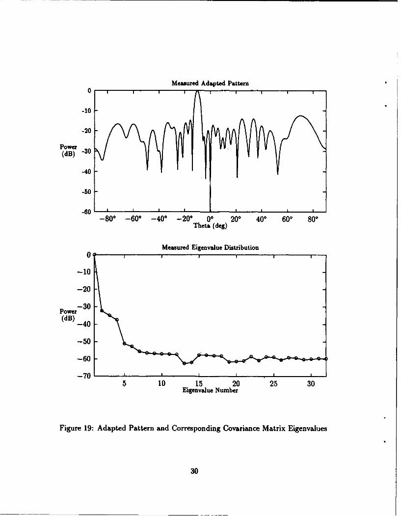
and 256 samples were used to estimate the covariance matrix. Figure 19 is the measured
adapted pattern and the corresponding eigenvalue distribution for a single narrowband
jammer located at -10 off broadside. Note that the pattern is the measured received
jammer power. The steering vector s is chosen to maximize the received desired signalat broadside with a 20 dB Taylor taper imposed. Thus, we expected a null at broadside
and a mainbeam at -10* when the array is scanned and only the jammer is on. Obtaining
the adapted response in this way provides a direct measure of jammer cancellation. The
main beam corresponds to maximum received jammer power and the null to jammercancellation. Figure 19 illustrates a jammer cancellation of 59 dB which is the full dynamic
range of the system.
The resultant adapted pattern in Figure 19 does not yield 20 dB sidelobes. This isexplained by the covariance matrix eigenvalues shown also in Figure 19. Ideally, there
should be only one large eigenvalue and the rest should be of equal, low magnitude. In our
case, the relatively large second, third, and fourth eigenvalues represent array errors (dc
offset, I/Q, third harmonic) and remaining eigenvalues represent different noise figures ofthe receiver channels. As a result, the weight vector w cannot be written in the idealized
form of Eq. (22), and the quiescent pattern structure is lost. A correction of the three
dominant array errors leads to the eigenvalue distribution shown in Figure 20. However,
the noise eigenvalues still differ and thus would spoil the sidelobe structure of any adapted
pattern.
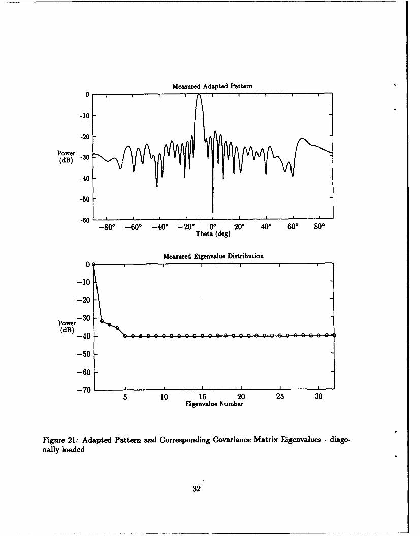
However, by diagonally loading the covariance matrix and thus artificially increasingthe noise component, we can make the noise structure more uniform. Figure 21 is the
measured adaptive pattern and the corresponding eigenvalue distribution as a result of
diagonal loading. Note that the jammer cancellation has decreased by 2 dB. This is to
be expected with a decrease in jammer to noise ratio.
This demonstrates the capability of simultaneously adaptively nulling the interferenceand maintaining low sidelobe performance. Again in this experiment, only the gain andphase errors were corrected and the SNR of the jammer was approximately 40 dB.
15

N ANALOG
DIGITAL
32DIGITALDGAMLO R DBF CONTROL/F1-:3 I BEAMFORMERVA=z•w,,x,, VAX
HEWLETT-PACKARDSYSTEM MPU
MI:
ANALOGOUT
Figure 1: Block diagram of the Digital Beamforming Testbed at Rome Laboratory
16

LOW NOISE AMPLIFIER
WAGE REJECTION FILTR
AGILE LO
IF FITE
FAMPLFIER
POWER WIDER
VIDEOAMP/
FIXELOLOW PASS FILER
AMD CONVERTER
Figure 2: Block diagram of an element receiver
17

Frequency Spectrum10
DESRED RESPONSE. f =250kHz0 IQ RESPONSE. &
HARMONIC RESPONSE-10 .0
ý-20 -DC OFFSET
-30
-50
-2 -1 0 1 2
Frequency (Hz) x 105
Figure 3: Spectrum for 1 A/D sampling frequency
Frequency Spectrum100 DESRED RESPONSE fQ=125kHz
-10IQ RESPONSE & DC OFFSET
-20 HARMONIC RESPONSE
S-30-
~-40O
-50-
-0 -2 -1 0 1 2Frequency (Hz) x 105
Figure 4: Spectrum for 1 A/D sampling frequency
18

Frequency Spectrum
DESIRED RESPONSE
0R fa = 15.625kHz
-10
S-20 DC OFFSET
30- I RES ONSEHARMONIC RESPONSE
-40-
-so-
-60
-2 -1 0 1 2Frequency (Hz) x 105
Figure 5: Spectrum for - A/D sampling frequency
Frequency Spectrum10
0 DESIRED REONSE fa1 =71.5 kHz
-10 DC OFFSET
-20o IQ RESPONSE
-30 HARMONIC RESPONSE
-50
-70
-2 -1 0 1 2Frequency (Hz) x 10l
Figure 6: Spectrum for • A/D sampling frequency - note spreading of spectral lines
19

ý' A B
2 m
(a, . am) e -siglr A
(b, b2 bM) eIb t -ms igal B
(nl(M no) nMt)) - noise
TV-
P
Figure 7: Two signals incident on antenna array
20

Gain VariationII I I I
4
2
Power(dB) 0
-2
-41 I
5 10 15 20 25 30Channel Number
Error Distribution0
DC Offset
-10 IQ Error3"d Harmonic..
-20
Power 30
-50
-601)•))
5 10 15 20 25 30Channel Number
Figure 8: Measured Gain Variations and Error Levels21

Phase Variation
1500
1000
Phase 00 l
(deg) 0
-500
-1000
_1500I I
IIII
5 10 15 20 25 30Channel Number
Figure 9: Measured Phase Variation
Thermal Noise Variation0
I
-10
-20
Power 30(dB) -30
-40
-50
-60 I I ,5 10 15 20 25 30
Channel Number
Figure 10: Measured Thermal Noise
22

Measured Antenna Pattern0
QuiescentDC Correctd
-10
-20
Power -30(dB)--
-40
-50
- 60 ,,-80 -600 -40* -200 00 200 400 600 80*Theta (deg)
Figure 11: Measured 40 dB Taylor - dc Corrected
23
Measured Antenna Pattern0
Quiescent -
DC & I/Q Corrected
-10
-20
Power(d0) -30
-40
-50
-60-80" -600 -400 -200 00 200 400 600 800
Theta (deg)
Figure 12: Measured 40 dB Taylor - dc and I/Q Corrected
24

0 Measured Antenna Pattern
Quiescent -
-10 All Corrections -
-20
Power 30n
(dB) -- '
-40
-50----. 60
,,,
-800 -600 -400 -20° 00 200 400 600 800Theta (deg)
Figure 13: Measured 40 dB Taylor - dc, I/Q and Third Harmonic Corrected
25

Gain Variation - 5.2 GHz
4
Power A(dB)
0
-2
-4I III I
5 10 15 20 25 30Channel Number
Error Distribution - 5.2 GHz
0DC Offset -
-10 IQ Error -
3rd Harmonic.
-20
Power- 3 0(dB)
-50
-601'''5 10 15 20 25 30
Channel Number
Figure 14: Measured Gain Variations and Error Levels - 5.2 GHz
26

Gain Variation - 5.4 GHsIII I
4
2
Power(dB) 0
-2
-4II l I I
5 10 15 20 25 30Channel Number
Error Distribution - 5.4 GHz0
DC Offset -
-10 3 IQ Error3"d Harmonic
-20
Power 30(dB) -3o
-40
-50
-60 I I I I I I5 10 15 20 25 30
Channel Number
Figure 15: Measured Gain Variations and Error Levels - 5.4 GHz
27

Gain Variation - 5.7 GHzIII I
4
2
Power(dB) 0
-2
-4
5 10 15 20 25 30Channel Number
Error Distribution - 5.7 GHz0
DC OffsetIQ Error-10 3 rd Harmonic
-20
Power_(dB) -30
-40
-605 10 15 20 25 30
Channel Number
Figure 16: Measured Gain Variations and Error Levels - 5.7 GHz
28

Direction of Arrival Estimations
0
-10
-20Amp.(dB)
-30
-40 -
-50 I a I
-30° -20° -100 00 100 200 300Theta
Figure 17: Measured MUSIC Algorithm Response - Sources 100 apart
Direction of Arrival Estimations - Comparison of Methods01
MUSIC -
SUM BEAMDIFF BEAM
Amp.(dB) -20
-30
-40 i I I
-300 -200 -100 00 100 200 300Theta
Figure 18: Comparison of DOA Estimations - Sources 1.7° apart
29.
Measured Adapted Pattern
0
-10
-20
Power(dB) -30
-40
-50-60
-80° -600 -40° -200 00 200 400 600 800Theta (deg)
Measured Eigenvalue Distribution
0
-10
-20
Power-30(dB) -40
-50
-60
-705 10 15 20 25 30
Eigenvalue Number
Figure 19: Adapted Pattern and Corresponding Covariance Matrix Eigenvalues
30

Eigenvalue Distribution0
-10
-20
-30Power(dB)
-40
-50
-60
5 10 15 20 25 30Eigenvalue Number
Figure 20: Covariance Matrix Eigenvalues after Correction of dc Offset, I/Q, and ThirdHarmonic Errors
31
Measured Adapted Pattern0
-10
-20
Power 3(dB) -30
-40
-50
-60-80° -60* -400 -200 00 200 400 600 800
Theta (deg)
Measured Eigenvalue Distribution
0P I
-10
-20
Power3 0
(dB) _40
-50
-60
-70 m I I
5 10 15 20 25 30Eigenvalue Number
Figure 21: Adapted Pattern and Corresponding Covariance Matrix Eigenvalues - diago-nally loaded
32

5 CONCLUSIONS
The purpose of this document was to provide a recent evaluation of the digital beam-forming testbed at Rome Laboratory. In doing so, we have completely documented the
dominant errors associated with the array's receive system. We have described the spec-tral and eigen analysis methods used to isolate and analyze the errors as well as illustrate
their effects on the antenna pattern. In addition, we have successfully demonstrated theability to implement the MUSIC and SMI algorithms used for super resolution and adap-tive nulling capabilities. As a result, we have illustrated enhanced array performance and
the flexibilty and power associated with digital beamforming.
33

References
[1] Applebaum, S.P. (1976) Adaptive arrays. IEEE Transactions on Antennas and Prop-
agation, pages 585-598,
[21 Eber, Louis (1988) Digital Beam Steering Antenna. Technical Report RADC-TR-88-83, Rome Laboratory, AD A200 030
[3] Langston, J. Leland (1988) Design Definition for a Digital Beamforming Processor.
Technical Report RADC-TR-88-86, Rome Laboratory, AD A196 983
[4] Pettersson, Lars Emil (1992) Adaptive Beamforming with Imperfect Arrays: Pat-
tern Effects and Their Partial Correction. Technical Report RL-TR-92-341, Rome
Laboratory, AD A267 079
[5] Schmidt, R. (1986) Multiple Emitter Location and Parameter Estimation. IEEE
Transactions on Antennas and Propagation, pages 275-280,
35

MWSSM
OF
ROME LABORATORY
Rome Laboratory plans and executes an interdisciplinaryprogram in resewarch, development, test, and technologytransition in support of Air Force Command, Control,Communications and Intelligence (C31) activities for allAir Force platforms. It also executes selectedacquisition programs in several areas of expertise.Technical and engineering support within areas ofcompetence is provided to ESC Program Offices (POs) andother ESC elements to perform effective acquisition ofC31 systems. In addition, Rome Laboratory's technologysupports other APF4C Product Divisions,, the Air Force usercommunity, and other DOD and non-DOD agencies. RomeLaboratory maintains technical competence and researchprograms in areas including, but not limited to,communications, command and control, battle management,intelligence information processing, computationalsciences and software producibility, wide areasurveillance/sensors, signal processing, solid statesciences, photonics, electromagnetic technology,superconductivity, and electronicreliability/maintainability and testability.


![i.,..,'l..].?Í '.rl' '..l.liÍ .T:.: -.' ].iI-i](https://img.pdfslide.us/doc/110x75/61caecaba6a82c3bbc46de5f/il-rl-lli-t-ii-i.jpg)