Embed Size (px)
Citation preview

RF and Microwave Power Technology, LLC 2380 Solitude Drive Reno, NV 89511 USA (775) 842-3280 [email protected] www.rfmpt.com
Specifications contained herein are subject to change without notice. RF and Microwave Power Technology, LLC assumes no liability for the use of this information.
© 2017 RF and Microwave Power Technology, LLC
Page 1 of 5 Doc #100099, Rev A, 8-16-2017
RFM225-400-350-HSD
225-400MHz 350W Class A/AB
High Performance Amplifier with High Speed Disable
The RFM225-400-350-HSD is a high gain, high power Class A/AB amplifier module designed for military
and commercial communications systems. It features fast output disable with <1µsec response time, and
includes numerous control and monitoring functions. It exhibits excellent gain flatness and linearity, and
is offered in a compact housing with a nickel plated copper base for best possible thermal performance.
Specifications (Two power supplies are required.)
Vsupply1 = +28VDC, IDQ = 3.3A, Vsupply2 = +50VDC, IDQ = 0.85A
Pout = 350W, Tbase = 50oC, Zload = 50Ω
Parameter Min Typ Max Units
Freq. Range 225 400 MHz
P1dB 350 See Fig. 4 W
Input Power -2.4 0 dBm
Gain 55.4 57.8 dB
Gain Flatness +/-0.4 +/-1.0 dB
Drain Current,
28VDC 3.3 3.5 A
Drain Current,
50VDC 13.1 14.4 A
Efficiency (output stage only)
49 53 %
IRL -20 -14 dB
f2 -47 -34 dBc
f3 -25 -12 dBc
IMD3 350W PEP, ∆f=100kHz
-40 -28 dBc
Dimensions 4.50 X 8.40 X 1.35
(114.30 X 213.36 X 34.29)
inch
(mm)
Class A/AB 350W linear amplifier
Fast output disable, <1µsec
VVA, over 30dB range
Analog temperature out
High temperature alarm
Independent MMIC disable
Output stage current sense
Temperature compensated bias
SMA input, N output connectors
Maximum Ratings Operation beyond these ratings may damage amplifier.
Parameter Value
Vsupply1 24-28VDC
Vsupply2 46-50VDC
Bias Current, 28VDC 3.5A
Bias Current, 50VDC 1.0A
Drain Current, 28VDC 3.5A
Drain current, 50VDC 15A
Load Mismatch* 3:1
Housing Base
Temperature (See important notes on
cooling, Page 5.)
60oC
Storage Temperature -40oC to 85oC
*All phase angles, 350W forward power,
current limited to 15A for 5 seconds
maximum.
RF and Microwave Power Technology, LLC 2380 Solitude Drive Reno, NV 89511 USA (775) 842-3280 [email protected] www.rfmpt.com
Specifications contained herein are subject to change without notice. RF and Microwave Power Technology, LLC assumes no liability for the use of this information.
© 2017 RF and Microwave Power Technology, LLC
Page 2 of 5 Doc #100099, Rev A, 8-16-2017
50
51
52
53
54
55
56
57
58
59
60
225 250 275 300 325 350 375 400
Frequency (MHz)
Ga
in (
dB
)
-60
-55
-50
-45
-40
-35
-30
-25
-20
225 250 275 300 325 350 375 400
Frequency (MHz)
IMD
3 (
dB
c)
350W
PEP
300W
PEP
-60
-50
-40
-30
-20
-10
0
225 250 275 300 325 350 375 400
Frequency (MHz)
Ha
rmo
nic
s (
dB
c)
f3
f2
200
225
250
275
300
325
350
375
400
225 250 275 300 325 350 375 400
Frequency (MHz)
P1
dB
an
d S
OA
(W
)
SOA
RFM225-400-350-HSD
225-400MHz 350W Class A/AB
High Performance Amplifier with High Speed Disable
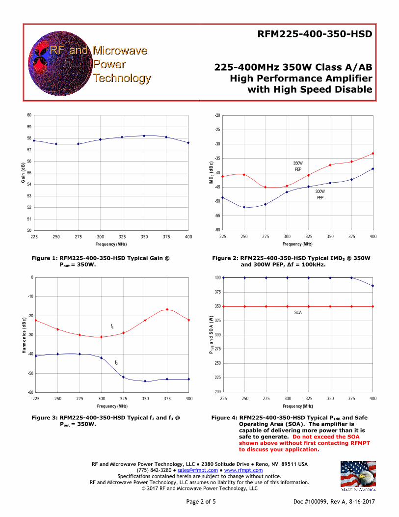
Figure 1: RFM225-400-350-HSD Typical Gain @ Pout = 350W.
Figure 2: RFM225-400-350-HSD Typical IMD3 @ 350W and 300W PEP, ∆f = 100kHz.
Figure 3: RFM225-400-350-HSD Typical f2 and f3 @ Pout = 350W.
Figure 4: RFM225-400-350-HSD Typical P1dB and Safe Operating Area (SOA). The amplifier is capable of delivering more power than it is safe to generate. Do not exceed the SOA shown above without first contacting RFMPT to discuss your application.

RF and Microwave Power Technology, LLC 2380 Solitude Drive Reno, NV 89511 USA (775) 842-3280 [email protected] www.rfmpt.com
Specifications contained herein are subject to change without notice. RF and Microwave Power Technology, LLC assumes no liability for the use of this information.
© 2017 RF and Microwave Power Technology, LLC
Page 3 of 5 Doc #100099, Rev A, 8-16-2017
RFM225-400-350-HSD
225-400MHz 350W Class A/AB
High Performance Amplifier with High Speed Disable
Amplifier Mounting Hole and RF Locations, and Mounting Screw Tightening Sequence

RF and Microwave Power Technology, LLC 2380 Solitude Drive Reno, NV 89511 USA (775) 842-3280 [email protected] www.rfmpt.com
Specifications contained herein are subject to change without notice. RF and Microwave Power Technology, LLC assumes no liability for the use of this information.
© 2017 RF and Microwave Power Technology, LLC
Page 4 of 5 Doc #100099, Rev A, 8-16-2017
RFM225-400-350-HSD
225-400MHz 350W Class A/AB
High Performance Amplifier with High Speed Disable
Interface Pins and Functions
1: VVA The voltage variable attenuator has a slope of approximately 14dB/volt, from 1.4 to 3.6VDC.
Maximum attenuation is reached by 4.4VDC. The acceptable control range is 0 to 5.0VDC. Do not
exceed 5.0VDC on this pin. The VVA control voltage should be set to zero volts during amplifier
power up and power down.
2: Temp Alarm This indicates an over-temperature condition, and is set to trip at a housing base
temperature of approximately +60oC. It is pulled up internally to +5VDC, and will pull down to 0V
at +60oC. This signal exhibits 5oC of hysteresis, and will reset to +5VDC at approximately +55oC.
3: Output Disable This is active high at +5VDC, and is TTL compatible. It disables the output and its
two drive stages simultaneously, and will reduce full rated output power to near zero* in <1µsec.
When set to 0VDC, the amplifier will return to within 0.25dB of full power in approximately 50µsec.
For further RF burst fidelity improvements, the end user may solder an electrolytic capacitor to the
+50VDC feedthru cap and ground stud next to it. RFMPT recommends a value of >4700uF.
* Due to feedback paths inherent in all stages of the amplifier, there will be a miniscule amount of
RF still present on the output even when bias has been disabled. For additional RF quieting, the
VVA may be set to maximum attenuation simultaneously with the Output Disable signal.
4: NC This pin has no internal connection and should be left floating.
5: Output Current Sense This is a DC signal scaled at 0.30V/A, and monitors the output transistor
only. Over-current protection should be enabled at >4.50VDC, or 15A output transistor current.
6: Temp Out This is an analog signal that is a nominal +0.75V at +25oC. The temp monitor IC has a
positive slope of 10mV/oC with increasing temperature. However, a temperature gradient and an
offset will exist between the temperature reported on this pin and the actual housing base
temperature directly under the output transistor (see bottom figure on Page 3). The reported slope
will be closer to 6.7mV/oC, rather than the native 10mV/oC of the IC. It is up to the end user to
properly characterize this signal’s response with their chosen cooling configuration.
7: MMIC Disable This is a supplementary disable pin, for additional amplifier quieting at the user’s
discretion. It exhibits approximately a 50usec delay for enable, and a 30usec delay for disable.
Due to the internal biasing resistor in the MMIC, there will be significant RF bleedthrough even
when the MMIC is disabled.
8: Interface GND All control and monitoring signals should be referenced to this pin. It is tied
internally to the amplifier ground plane. A minimum of 20 gauge wire is recommended for best
grounding.
9: NC This pin has no internal connection and should be left floating.

RF and Microwave Power Technology, LLC 2380 Solitude Drive Reno, NV 89511 USA (775) 842-3280 [email protected] www.rfmpt.com
Specifications contained herein are subject to change without notice. RF and Microwave Power Technology, LLC assumes no liability for the use of this information.
© 2017 RF and Microwave Power Technology, LLC
Page 5 of 5 Doc #100099, Rev A, 8-16-2017
RFM225-400-350-HSD
225-400MHz 350W Class A/AB
High Performance Amplifier with High Speed Disable
Instructions for Amplifier Use
1) IMPORTANT: This amplifier uses a single high power output transistor which will dissipate up to 375W even
into a well matched 50 ohm load. Peak dissipation will occur between 400 and 450MHz, and very careful
attention must be paid to proper amplifier cooling or transistor lifetime will be substantially reduced and will
not be covered under warranty. The maximum allowed housing base temperature directly under the center of
the output transistor is 60oC (see bottom figure on Page 3 for thermal qualification point location). Due to
amplifier cooling requirements, a high performance thermal compound (Wakefield Type 122 or better) must
be used. Standard performance thermal compounds will be inadequate in air cooled systems, and their use
will void the warranty. Apply the thermal compound to the bottom of the amplifier housing. Thinner is better,
but ensure that when mounted to your heatsink, contact across the entire module base is made. Gaps and
air bubbles will significantly reduce cooling, leading to possible amplifier damage. Use 12 #6-32 or M4 screws
to mount the amplifier to your heatsink. Refer to the figure on the bottom of Page 3 for the proper order in
which to torque the mounting screws. 2) Guarantee sufficient airflow through the heatsink fins to keep the maximum housing base temperature at or
less than 60oC. Contact RFMPT for details on how to qualify your heatsink’s performance, if needed.
3) Connect a proper signal source to the RF In connector, and desired load to the RF Out connector. Torque
connectors to industry standards for the types supplied with the amplifier.
4) Connect +50VDC to the bottom feedthru connector on the output end of the amplifier housing. Use a
minimum of 14 gauge wire (12 gauge preferred). Connect +28VDC to the top feedthru connector on the
output end of the amplifier housing. Use a minimum of 18 gauge wire. Ensure that the DC supply voltages
are within the ranges specified in the Maximum Ratings section. It is preferred to ground the amplifier
through the heatsink for lowest impedance ground. In addition, a safety ground should be connected to the
ground stud on the output end of the amplifier housing. Use a minimum of 12 gauge wire for this connection. 5) Apply desired signals/monitoring lines to the interface pins in the DB-9 connector. Refer to the Interface Pins
and Functions section for signal descriptions, limits, and timing requirements.
6) Apply +50VDC, then +28VDC, then sufficient RF drive to achieve desired output level. The maximum
amplifier RF input power is 0dBm. This amplifier is designed to operate in a non-saturated linear mode only.
Regardless of the input power, ensure that the Safe Operating Area (SOA) power level indicated in Figure 4 is
not exceeded, or amplifier damage may occur, and will void the warranty.
7) To disconnect the amplifier, first remove the RF drive, then +28VDC, then +50VDC, then the RF connections.
Contact the factory at [email protected] with any questions, or for special options, testing requirements, and/or
operating conditions not specified in this document.
Document Control
Revision Date Notes
A 8-16-2017 Initial release.