Embed Size (px)
Citation preview
8/13/2019 Regulador Voltage 3.3v Xbox360
http://slidepdf.com/reader/full/regulador-voltage-33v-xbox360 1/18
© Semiconductor Components Industries, LLC, 2012
April, 2012−
Rev. 24
1 Publication Order Number:
NCP1117/D
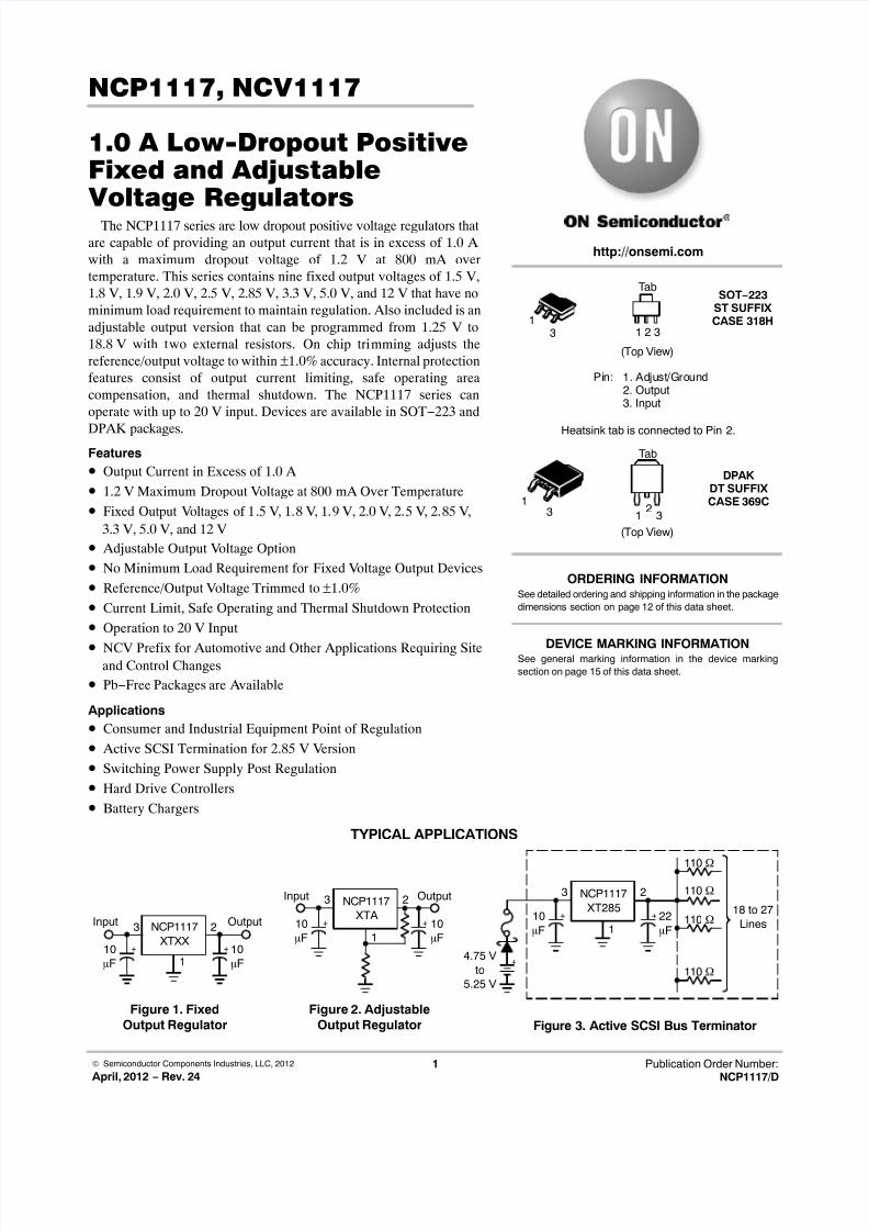
NCP1117, NCV1117
1.0 A Low-Dropout PositiveFixed and AdjustableVoltage Regulators
The NCP1117 series are low dropout positive voltage regulators that
are capable of providing an output current that is in excess of 1.0 A
with a maximum dropout voltage of 1.2 V at 800 mA over
temperature. This series contains nine fixed output voltages of 1.5 V,
1.8 V, 1.9 V, 2.0 V, 2.5 V, 2.85 V, 3.3 V, 5.0 V, and 12 V that have no
minimum load requirement to maintain regulation. Also included is an
adjustable output version that can be programmed from 1.25 V to
18.8 V with two external resistors. On chip trimming adjusts the
reference/output voltage to within ±1.0% accuracy. Internal protection
features consist of output current limiting, safe operating area
compensation, and thermal shutdown. The NCP1117 series can
operate with up to 20 V input. Devices are available in SOT−223 and
DPAK packages.Features
• Output Current in Excess of 1.0 A
• 1.2 V Maximum Dropout Voltage at 800 mA Over Temperature
• Fixed Output Voltages of 1.5 V, 1.8 V, 1.9 V, 2.0 V, 2.5 V, 2.85 V,
3.3 V, 5.0 V, and 12 V
• Adjustable Output Voltage Option
• No Minimum Load Requirement for Fixed Voltage Output Devices
• Reference/Output Voltage Trimmed to ±1.0%
• Current Limit, Safe Operating and Thermal Shutdown Protection
• Operation to 20 V Input
• NCV Prefix for Automotive and Other Applications Requiring Siteand Control Changes
• Pb−Free Packages are Available
Applications
• Consumer and Industrial Equipment Point of Regulation
• Active SCSI Termination for 2.85 V Version
• Switching Power Supply Post Regulation
• Hard Drive Controllers
• Battery Chargers
10
F1
2 Output
10
F
3Input NCP1117
XTXX+ +
Figure 1. Fixed
Output Regulator
10
F1
2 Output
10
F
3Input NCP1117
XTA+ +
Figure 2. Adjustable
Output Regulator
22
F1
2
10
F
3 NCP1117
XT285+ +
110
110
110
110
4.75 V
to
5.25 V
+
18 to 27
Lines
Figure 3. Active SCSI Bus Terminator
TYPICAL APPLICATIONS
SOT−223ST SUFFIX CASE 318H1
3
DPAK DT SUFFIX CASE 369C
Pin: 1. Adjust/Ground2. Output3. Input
13
Heatsink tab is connected to Pin 2.
See detailed ordering and shipping information in the package
dimensions section on page 12 of this data sheet.
ORDERING INFORMATION
See general marking information in the device marking
section on page 15 of this data sheet.
DEVICE MARKING INFORMATION
1 2 3
12
3
Tab
Tab
(Top View)
(Top View)
http://onsemi.com
8/13/2019 Regulador Voltage 3.3v Xbox360
http://slidepdf.com/reader/full/regulador-voltage-33v-xbox360 2/18
NCP1117, NCV1117
http://onsemi.com
2
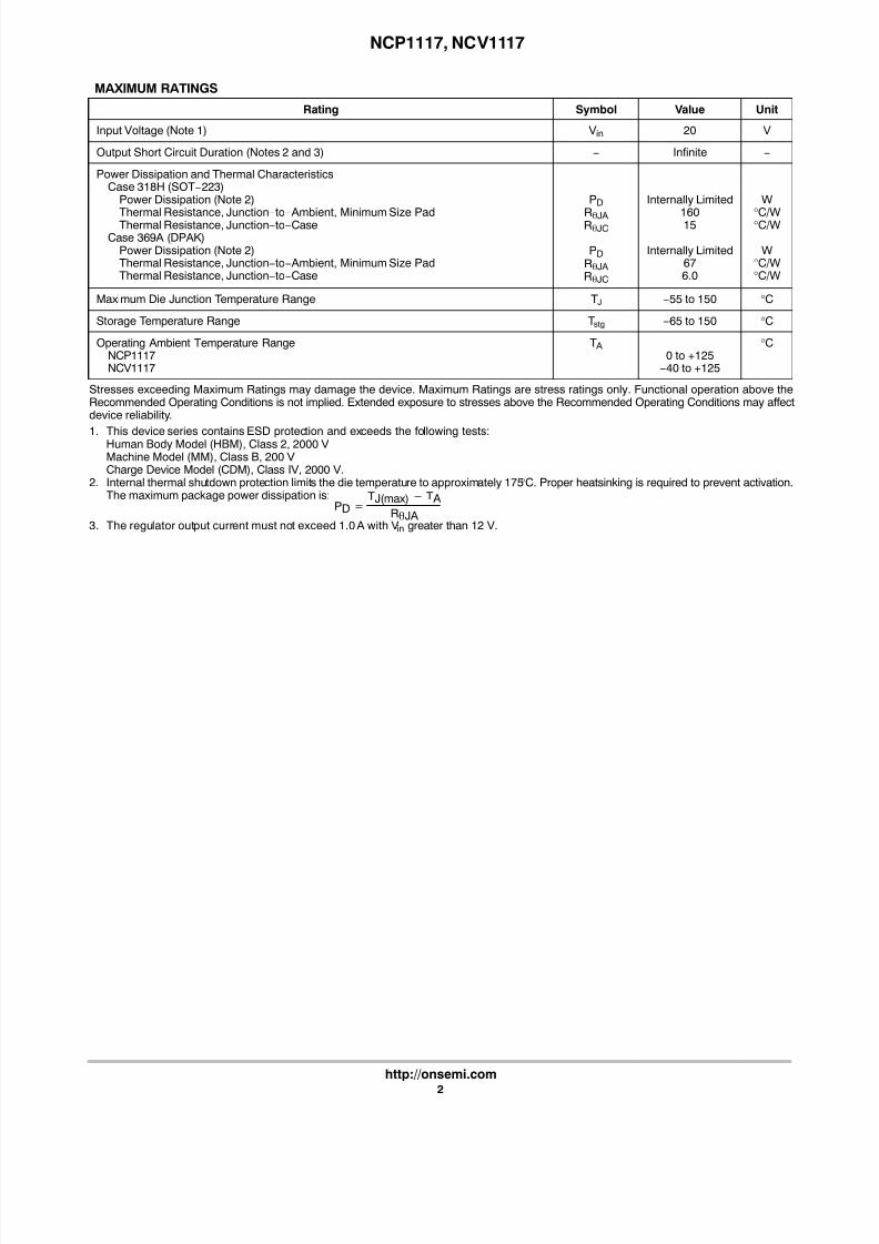
MAXIMUM RATINGS
Rating Symbol Value Unit
Input Voltage (Note 1) Vin 20 V
Output Short Circuit Duration (Notes 2 and 3) − Infinite −
Power Dissipation and Thermal CharacteristicsCase 318H (SOT−223)
Power Dissipation (Note 2)
Thermal Resistance, Junction−
to−
Ambient, Minimum Size PadThermal Resistance, Junction−to−CaseCase 369A (DPAK)
Power Dissipation (Note 2)Thermal Resistance, Junction−to− Ambient, Minimum Size PadThermal Resistance, Junction−to−Case
PD
RJARJC
PDRJARJC
Internally Limited
16015
Internally Limited676.0
W°
C/W°C/W
W°C/W°C/W
Maximum Die Junction Temperature Range TJ −55 to 150 °C
Storage Temperature Range Tstg −65 to 150 °C
Operating Ambient Temperature RangeNCP1117NCV1117
T A0 to +125
−40 to +125
°C
Stresses exceeding Maximum Ratings may damage the device. Maximum Ratings are stress ratings only. Functional operation above theRecommended Operating Conditions is not implied. Extended exposure to stresses above the Recommended Operating Conditions may affectdevice reliability.
1. This device series contains ESD protection and exceeds the following tests:Human Body Model (HBM), Class 2, 2000 VMachine Model (MM), Class B, 200 VCharge Device Model (CDM), Class IV, 2000 V.
2. Internal thermal shutdown protection limits the die temperature to approximately 175°C. Proper heatsinking is required to prevent activation.The maximum package power dissipation is:
PD TJ(max) T A
RJA3. The regulator output current must not exceed 1.0 A with Vin greater than 12 V.
8/13/2019 Regulador Voltage 3.3v Xbox360
http://slidepdf.com/reader/full/regulador-voltage-33v-xbox360 3/18
NCP1117, NCV1117
http://onsemi.com
3
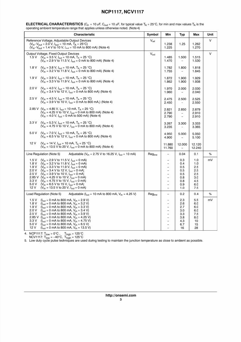
ELECTRICAL CHARACTERISTICS (Cin = 10 F, Cout = 10 F, for typical value T A = 25°C, for min and max values T A is the
operating ambient temperature range that applies unless otherwise noted. (Note 4)
Characteristic Symbol Min Typ Max Unit
Reference Voltage, Adjustable Output Devices(Vin –Vout = 2.0 V, Iout = 10 mA, T A = 25°C)(Vin –Vout = 1.4 V to 10 V, Iout = 10 mA to 800 mA) (Note 4)
Vref
1.2381.225
1.25−
1.2621.270
V
Output Voltage, Fixed Output Devices1.5 V (Vin = 3.5 V, Iout = 10 mA, T A = 25 °C)
(Vin = 2.9 V to 11.5 V, Iout = 0 mA to 800 mA) (Note 4)
1.8 V (Vin = 3.8 V, Iout = 10 mA, T A = 25 °C)(Vin = 3.2 V to 11.8 V, Iout = 0 mA to 800 mA) (Note 4)
1.9 V (Vin = 3.9 V, Iout = 10 mA, T A = 25 °C)(Vin = 3.3 V to 11.9 V, Iout = 0 mA to 800 mA) (Note 4)
2.0 V (Vin = 4.0 V, Iout = 10 mA, T A = 25 °C)(Vin = 3.4 V to 12 V, Iout = 0 mA to 800 mA) (Note 4)
2.5 V (Vin = 4.5 V, Iout = 10 mA, T A = 25 °C)(Vin = 3.9 V to 10 V, Iout = 0 mA to 800 mA,) (Note 4)
2.85 V (Vin = 4.85 V, Iout = 10 mA, T A = 25 °C)(Vin = 4.25 V to 10 V, Iout = 0 mA to 800 mA) (Note 4)(Vin = 4.0 V, Iout = 0 mA to 500 mA) (Note 4)
3.3 V (Vin = 5.3 V, Iout = 10 mA, T A = 25 °C)(Vin = 4.75 V to 10 V, Iout = 0 mA to 800 mA) (Note 4)
5.0 V (Vin = 7.0 V, Iout = 10 mA, T A = 25 °C)(Vin = 6.5 V to 12 V, Iout = 0 mA to 800 mA) (Note 4)
12 V (Vin = 14 V, Iout = 10 mA, T A = 25 °C)(Vin = 13.5 V to 20 V, Iout = 0 mA to 800 mA) (Note 4)
Vout
1.485
1.470
1.7821.755
1.8721.862
1.9701.960
2.4752.450
2.8212.7902.790
3.2673.235
4.9504.900
11.88011.760
1.500
−
1.800−
1.9001.900
2.000−
2.500−
2.850−
−
3.300−
5.000−
12.000−
1.515
1.530
1.8181.845
1.9291.938
2.0302.040
2.5252.550
2.8792.9102.910
3.3333.365
5.0505.100
12.12012.240
V
Line Regulation (Note 5) Adjustable (Vin = 2.75 V to 16.25 V, Iout = 10 mA) Regline − 0.04 0.1 %
1.5 V (Vin = 2.9 V to 11.5 V, Iout = 0 mA)1.8 V (Vin = 3.2 V to 11.8 V, Iout = 0 mA)1.9 V (Vin = 3.3 V to 11.9 V, Iout = 0 mA)2.0 V (Vin = 3.4 V to 12 V, Iout = 0 mA)2.5 V (Vin = 3.9 V to 10 V, Iout = 0 mA)2.85 V (Vin = 4.25 V to 10 V, Iout = 0 mA)
3.3 V (Vin = 4.75 V to 15 V, Iout = 0 mA)5.0 V (Vin = 6.5 V to 15 V, Iout = 0 mA)12 V (Vin = 13.5 V to 20 V, Iout = 0 mA)
−
−
−
−
−
−
−
−
−
0.30.40.50.50.50.8
0.80.91.0
1.01.02.52.52.53.0
4.56.07.5
mV
Load Regulation (Note 5) Adjustable (Iout = 10 mA to 800 mA, Vin = 4.25 V) Regline − 0.2 0.4 %
1.5 V (Iout = 0 mA to 800 mA, Vin = 2.9 V)1.8 V (Iout = 0 mA to 800 mA, Vin = 3.2 V)1.9 V (Iout = 0 mA to 800 mA, Vin = 3.3 V)2.0 V (Iout = 0 mA to 800 mA, Vin = 3.4 V)2.5 V (Iout = 0 mA to 800 mA, Vin = 3.9 V)2.85 V (Iout = 0 mA to 800 mA, Vin = 4.25 V)3.3 V (Iout = 0 mA to 800 mA, Vin = 4.75 V)5.0 V (Iout = 0 mA to 800 mA, Vin = 6.5 V)12 V (Iout = 0 mA to 800 mA, Vin = 13.5 V)
−
−
−
−
−
−
−
−
−
2.32.62.73.03.33.84.36.716
5.56.06.06.07.58.0101528
mV
4. NCP1117: Tlow = 0°C , Thigh = 125°CNCV1117: Tlow = −40°C, Thigh = 125°C
5. Low duty cycle pulse techniques are used during testing to maintain the junction temperature as close to ambient as possible.
8/13/2019 Regulador Voltage 3.3v Xbox360
http://slidepdf.com/reader/full/regulador-voltage-33v-xbox360 4/18
NCP1117, NCV1117
http://onsemi.com
4
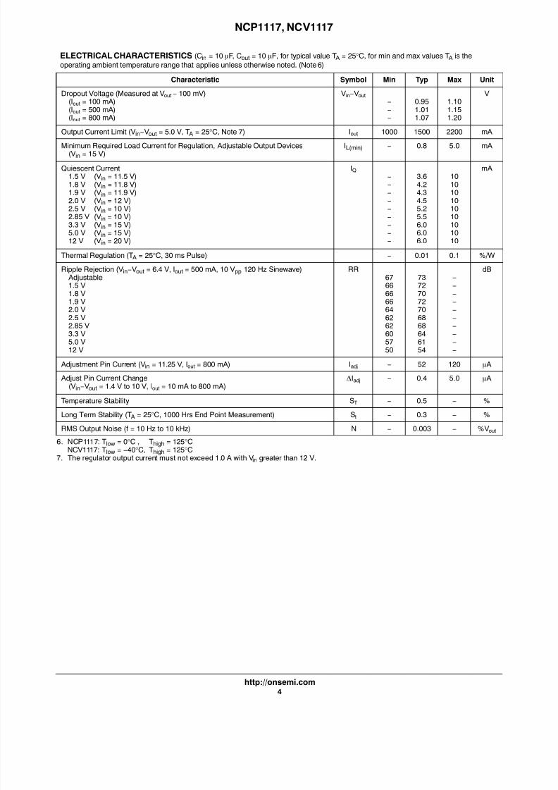
ELECTRICAL CHARACTERISTICS (Cin = 10 F, Cout = 10 F, for typical value T A = 25°C, for min and max values T A is the
operating ambient temperature range that applies unless otherwise noted. (Note 6)
Characteristic Symbol Min Typ Max Unit
Dropout Voltage (Measured at Vout − 100 mV)(Iout = 100 mA)(Iout = 500 mA)(Iout = 800 mA)
Vin−Vout
−
−
−
0.951.011.07
1.101.151.20
V
Output Current Limit (Vin−Vout = 5.0 V, T A = 25°C, Note 7) Iout 1000 1500 2200 mA
Minimum Required Load Current for Regulation, Adjustable Output Devices(Vin = 15 V)
IL(min) − 0.8 5.0 mA
Quiescent Current1.5 V (Vin = 11.5 V)1.8 V (Vin = 11.8 V)1.9 V (Vin = 11.9 V)2.0 V (Vin = 12 V)2.5 V (Vin = 10 V)2.85 V (Vin = 10 V)3.3 V (Vin = 15 V)5.0 V (Vin = 15 V)12 V (Vin = 20 V)
IQ−
−
−
−
−
−
−
−
−
3.64.24.34.55.25.56.06.06.0
101010101010101010
mA
Thermal Regulation (T A = 25°C, 30 ms Pulse) − 0.01 0.1 %/W
Ripple Rejection (Vin−Vout = 6.4 V, Iout = 500 mA, 10 Vpp 120 Hz Sinewave)
Adjustable1.5 V1.8 V1.9 V2.0 V2.5 V2.85 V3.3 V5.0 V12 V
RR
67666666646262605750
73727072706868646154
−
−
−
−
−
−
−
−
−
−
dB
Adjustment Pin Current (Vin = 11.25 V, Iout = 800 mA) Iadj − 52 120 A
Adjust Pin Current Change(Vin−Vout = 1.4 V to 10 V, Iout = 10 mA to 800 mA)
Iadj − 0.4 5.0 A
Temperature Stability ST − 0.5 − %
Long Term Stability (T A = 25°C, 1000 Hrs End Point Measurement) St −
0.3 −
%
RMS Output Noise (f = 10 Hz to 10 kHz) N − 0.003 − %Vout
6. NCP1117: Tlow = 0°C , Thigh = 125°CNCV1117: Tlow = −40°C, Thigh = 125°C
7. The regulator output current must not exceed 1.0 A with Vin greater than 12 V.
8/13/2019 Regulador Voltage 3.3v Xbox360
http://slidepdf.com/reader/full/regulador-voltage-33v-xbox360 5/18
NCP1117, NCV1117
http://onsemi.com
5
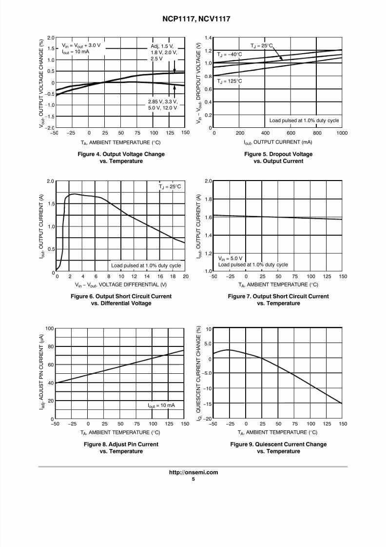
V i n − V
o u
t , D R
O P O U T V O L T A G E ( V )
T A, AMBIENT TEMPERATURE (°C)
I a d j ,
A D J U S T P I N C U R R E N T ( A )
Iout = 10 mA
0
20
40
60
80
100
Figure 4. Output Voltage Change
vs. Temperature
Figure 5. Dropout Voltage
vs. Output Current
Figure 6. Output Short Circuit Current
vs. Differential Voltage
Figure 7. Output Short Circuit Current
vs. Temperature
Figure 8. Adjust Pin Current
vs. Temperature
Figure 9. Quiescent Current Change
vs. Temperature
0
0.5
1.0
1.5
2.0
0 2 4 6 8 10 12 14 16 18 20
Load pulsed at 1.0% duty cycle
Vin
− Vout
, VOLTAGE DIFFERENTIAL (V)
I o u
t , O U T P U T C U R R E N T ( A )
TJ = 25°C
0
0.2
0.4
0.6
0.8
1.0
1.2
1.4
0 200 400 600 800 1000
Load pulsed at 1.0% duty cycle
Iout, OUTPUT CURRENT (mA)
TJ = −40°C
TJ = 25°C
TJ = 125°C
V o u
t , O U T P U T
V O L T A G E C H A N G E ( % )
−2.0
−1.5
−1.0
−
0.5
0
0.5
1.0
1.5
2.0
−50 −25 0 25 50 75 100 125 150
T A, AMBIENT TEMPERATURE (°C)
Vin = Vout + 3.0 V
Iout = 10 mA Adj, 1.5 V,
1.8 V, 2.0 V,
2.5 V
2.85 V, 3.3 V,
5.0 V, 12.0 V
1.0
1.2
1.4
1.6
1.8
2.0
−50 −25 0 25 50 75 100 125 150
−20
−15
−10
−5.0
0
5.0
10
−50 −25 0 25 50 75 100 125 150
T A
, AMBIENT TEMPERATURE (°C)
I o u
t , O U T P U T C U R R E N T ( A )
Vin = 5.0 V
Load pulsed at 1.0% duty cycle
T A, AMBIENT TEMPERATURE (°C)
I Q ,
Q U I E S C E N T
C U R R E N T C H A N G E ( % )
−50 −25 0 25 50 75 100 125 150
8/13/2019 Regulador Voltage 3.3v Xbox360
http://slidepdf.com/reader/full/regulador-voltage-33v-xbox360 6/18
NCP1117, NCV1117
http://onsemi.com
6
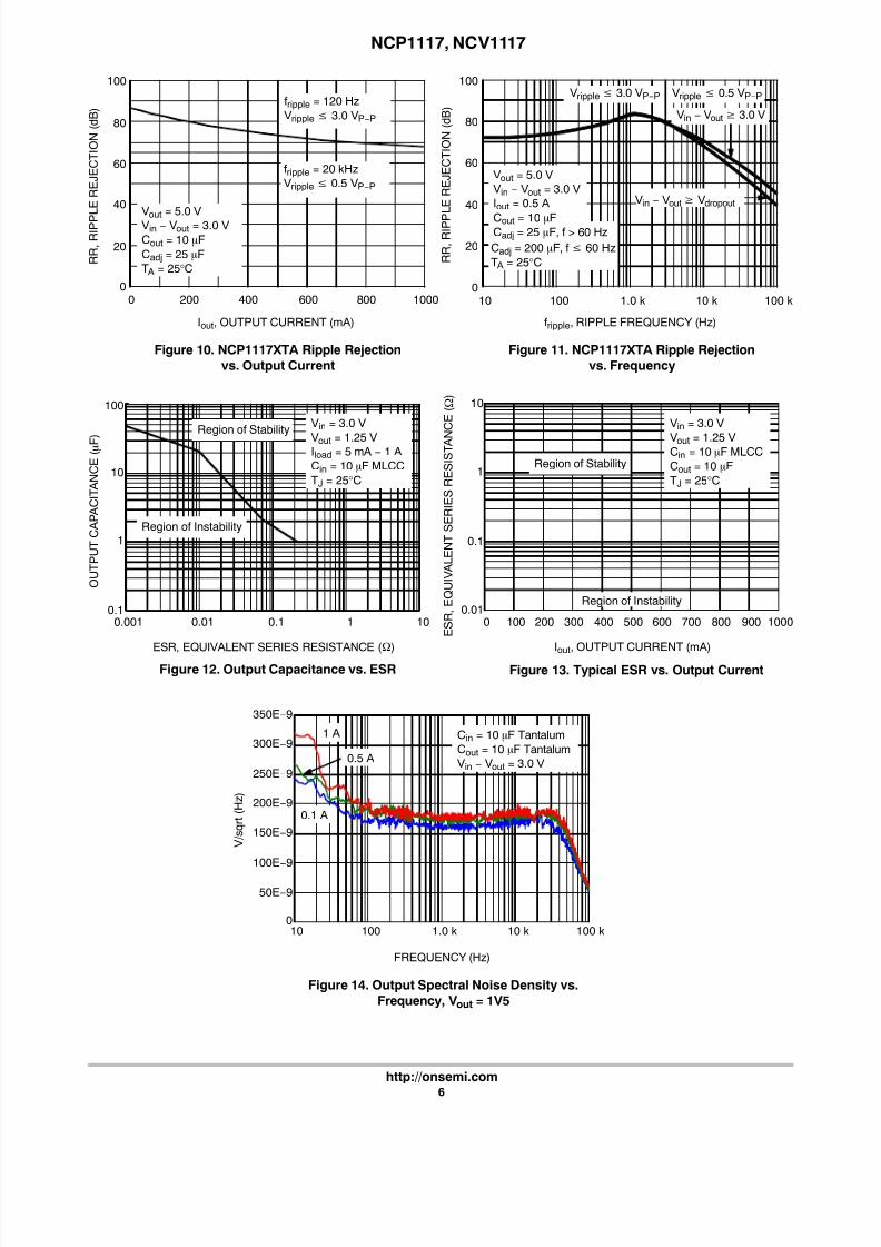
0
20
40
60
80
100
10 100 1.0 k 10 k 100 k
0
20
40
60
80
100
0 200 400 600 800 1000
Iout, OUTPUT CURRENT (mA)
R R
, R I P P
L E R E J E C T I O N ( d B )
f ripple = 20 kHz
Vripple 0.5 VP−P
Vout
= 5.0 V
Vin − Vout = 3.0 V
Cout = 10 F
Cadj = 25 F
T A = 25°C
f ripple, RIPPLE FREQUENCY (Hz)
R R
, R I P P
L E R E J E C T I O N ( d B )
Vout = 5.0 V
Vin − Vout = 3.0 V
Iout = 0.5 A
Cout = 10 FCadj = 25 F, f > 60 Hz
Vripple 3.0 VP−P Vripple 0.5 VP−P
Vin − Vout 3.0 V
Figure 10. NCP1117XTA Ripple Rejection
vs. Output Current
Figure 11. NCP1117XTA Ripple Rejection
vs. Frequency
Figure 12. Output Capacitance vs. ESR Figure 13. Typical ESR vs. Output Current
f ripple = 120 Hz
Vripple 3.0 VP−P
Vin − Vout Vdropout
Cadj = 200 F, f 60 Hz
T A = 25°C
0.1
1
10
100
0.001 0.01 0.1 1 10
ESR, EQUIVALENT SERIES RESISTANCE ()
O U T P U T C A P A C I T A N C E ( F )
Vin = 3.0 V
Vout = 1.25 VIload = 5 mA − 1 A
Cin = 10 F MLCC
TJ = 25°C
Region of Instability
Region of Stability
0.01
0.1
1
10
0 100 500 900 1000
Iout, OUTPUT CURRENT (mA)
E S R
, E Q U I V A L E N T S E R I E S R E S I S T A N
C E ( )
Vin = 3.0 V
Vout = 1.25 VCin = 10 F MLCC
Cout = 10 F
TJ = 25°C
Region of Instability
Region of Stability
200 600300 700400 800
0
50E−9
100E−9
150E−9
200E−9
250E−9
10 100 1.0 k 10 k 100 k
FREQUENCY (Hz)
V / s q r t
( H z
)
Cin = 10 F Tantalum
Cout = 10 F Tantalum
Vin − Vout = 3.0 V
Figure 14. Output Spectral Noise Density vs.
Frequency, V out = 1V5
300E−9
350E−9
1 A
0.5 A
0.1 A
8/13/2019 Regulador Voltage 3.3v Xbox360
http://slidepdf.com/reader/full/regulador-voltage-33v-xbox360 7/18
NCP1117, NCV1117
http://onsemi.com
7
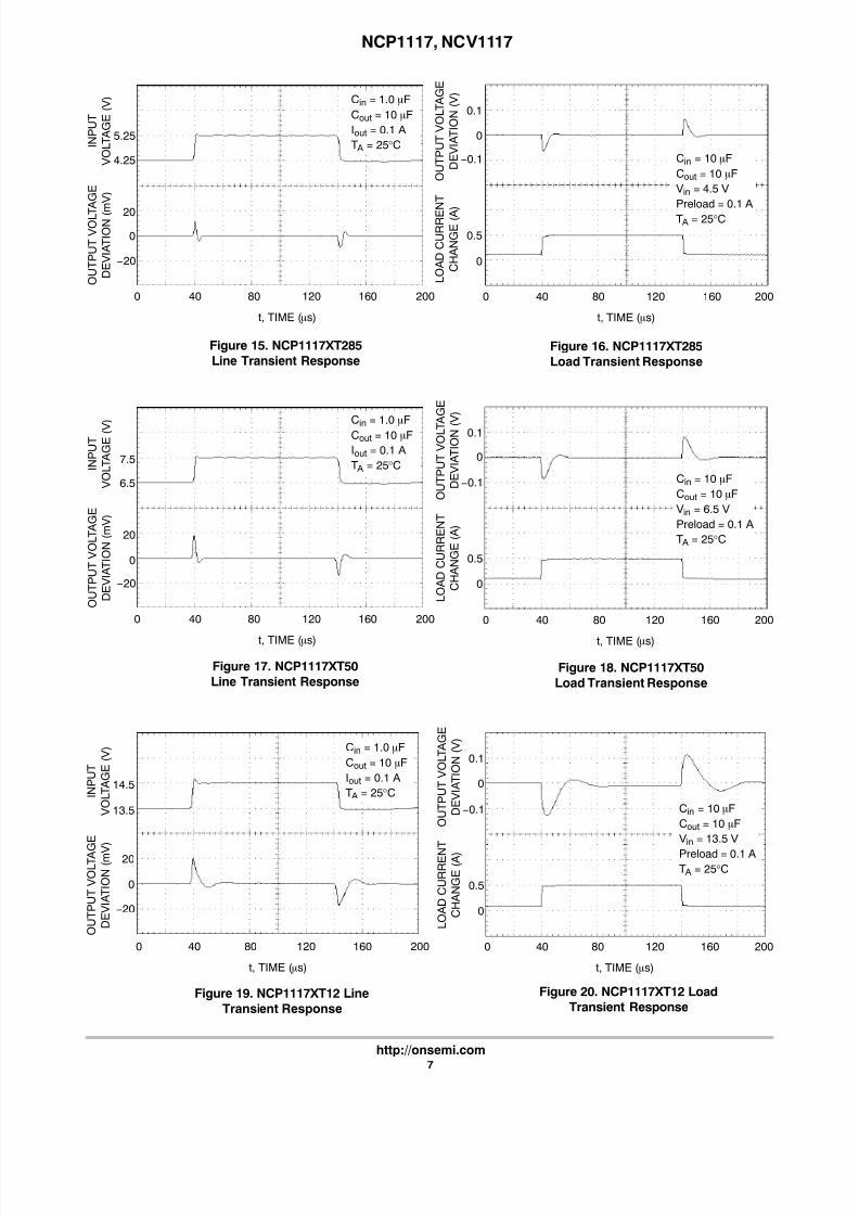
t, TIME (s)
−20
0
7.5
6.5
0 40 80 120 160
O U T P U T V O L T A G E
D E V I A T I O N ( m V )
I N P U T
V O L T A G E ( V
)
200
20
Figure 15. NCP1117XT285
Line Transient ResponseFigure 16. NCP1117XT285
Load Transient Response
Figure 17. NCP1117XT50
Line Transient ResponseFigure 18. NCP1117XT50
Load Transient Response
Cin = 10 F
Cout = 10 F
Vin = 6.5 V
Preload = 0.1 A
T A = 25°C
t, TIME (s)
0
0.5
0
0.1
−0.1
0 40 80 120 160
L O A D C U R R E N T
C H A N G E ( A )
O U T P U T V O L T A G E
D E V I A T I O N ( V )
200
Cin = 10 F
Cout = 10 F
Vin = 4.5 V
Preload = 0.1 A
T A = 25°C
t, TIME (s)
0
0.5
0
0.1
−0.1
0 40 80 120 160
L O A D C U R R E
N T
C H A N G E ( A
)
O U T P U T V O L T A G E
D E V I A T I O N ( V )
200
t, TIME (s)
−20
0
5.25
4.25
0 40 80 120 160
O U T P U T V O L T
A G E
D E V I A T I O N ( m
V )
I N P U T
V O L T A G E ( V )
200
Cin = 1.0 F
Cout = 10 F
Iout = 0.1 A
T A = 25°C
20
Cin
= 1.0 F
Cout = 10 F
Iout = 0.1 A
T A = 25°C
Figure 19. NCP1117XT12 Line
Transient Response
Figure 20. NCP1117XT12 Load
Transient Response
t, TIME (s)
Cin = 10 F
Cout = 10 F
Vin = 13.5 V
Preload = 0.1 AT A = 25°C
0
0.5
0
0.1
−0.1
0 40 80 120 160 200
L O A D C U R R E N
T
C H A N G E ( A )
O U T P U T V O L T A G E
D E V I A T I O N ( V )
t, TIME (s)
−20
0
14.5
13.5
0 40 80 120 160
O U T P U T V O L T A G E
D E V I A T I O N ( m V )
I N P U T
V O L T A G E ( V )
200
20
Cin = 1.0 F
Cout = 10 F
Iout = 0.1 A
T A = 25°C
8/13/2019 Regulador Voltage 3.3v Xbox360
http://slidepdf.com/reader/full/regulador-voltage-33v-xbox360 8/18
NCP1117, NCV1117
http://onsemi.com
8
60
80
100
120
140
160
180
0.4
0.6
0.8
1.0
1.2
1.4
1.6
0 10 20 3025155.0
L, LENGTH OF COPPER (mm)
PD(max) for T A = 50°C
40
50
60
70
80
90
100
0 10 20 3025155.0
L, LENGTH OF COPPER (mm)
0.6
0.8
1.0
1.2
1.4
1.6
Figure 21. SOT−223 Thermal Resistance and Maximum
Power Dissipation vs. P.C.B. Copper Length
R J A ,
T H E R
M A L R E S I S T A N C E
,
J U N C T I O
N −
T O −
A I R ( ° C W )
P D ,
M A X I M U M P
O W E R D I S S I P A T I O N ( W )
R J A ,
T H E R M A L R E S I S T A N C E ,
J U N C T I O N −
T O −
A I R ( ° C W )
0.4
Figure 22. DPAK Thermal Resistance and Maximum
Power Dissipation vs. P.C.B. Copper Length
Minimum
Size Pad
P D ,
M A X I M U M P O W E R D I S S I P A T I O N
( W )
LÎ Î Î Î
Î Î Î Î
Î Î Î Î
Î Î Î Î
2.0 oz. Copper
RJA
Minimum
Size Pad
PD(max) for T A = 50°C
L
RJA
L
L
2.0 oz. Copper
Î Î Î
Î Î Î
Î Î Î
8/13/2019 Regulador Voltage 3.3v Xbox360
http://slidepdf.com/reader/full/regulador-voltage-33v-xbox360 9/18
NCP1117, NCV1117
http://onsemi.com
9
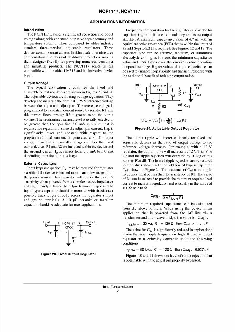
APPLICATIONS INFORMATION
Introduction
The NCP1117 features a significant reduction in dropout
voltage along with enhanced output voltage accuracy and
temperature stability when compared to older industry
standard three−terminal adjustable regulators. These
devices contain output current limiting, safe operating area
compensation and thermal shutdown protection makingthem designer friendly for powering numerous consumer
and industrial products. The NCP1117 series is pin
compatible with the older LM317 and its derivative device
types.
Output Voltage
The typical application circuits for the fixed and
adjustable output regulators are shown in Figures 23 and 24.
The adjustable devices are floating voltage regulators. They
develop and maintain the nominal 1.25 V reference voltage
between the output and adjust pins. The reference voltage is
programmed to a constant current source by resistor R1, and
this current flows through R2 to ground to set the outputvoltage. The programmed current level is usually selected to
be greater than the specified 5.0 mA minimum that is
required for regulation. Since the adjust pin current, Iadj, is
significantly lower and constant with respect to the
programmed load current, it generates a small output
voltage error that can usually be ignored. For the fixed
output devices R1 and R2 are included within the device and
the ground current Ignd, ranges from 3.0 mA to 5.0 mA
depending upon the output voltage.
External Capacitors
Input bypass capacitor Cin may be required for regulator
stability if the device is located more than a few inches from
the power source. This capacitor will reduce the circuit’s
sensitivity when powered from a complex source impedance
and significantly enhance the output transient response. The
input bypass capacitor should be mounted with the shortest
possible track length directly across the regulator’s input
and ground terminals. A 10 F ceramic or tantalum
capacitor should be adequate for most applications.
Figure 23. Fixed Output Regulator
1
2 Output3Input NCP1117
XTXX+ +
CoutCinIgnd
Frequency compensation for the regulator is provided by
capacitor Cout and its use is mandatory to ensure output
stability. A minimum capacitance value of 4.7 F with an
equivalent series resistance (ESR) that is within the limits of
33 m (typ) to 2.2 is required. See Figures 12 and 13. The
capacitor type can be ceramic, tantalum, or aluminum
electrolytic as long as it meets the minimum capacitancevalue and ESR limits over the circuit’s entire operating
temperature range. Higher values of output capacitance can
be used to enhance loop stability and transient response with
the additional benefit of reducing output noise.
Figure 24. Adjustable Output Regulator
1
2 Output3Input NCP1117
XTA+ +
CoutCin
Iadj
R2+
Cadj
Vref R1
Vout Vref 1 R2R1 Iadj R2
The output ripple will increase linearly for fixed and
adjustable devices as the ratio of output voltage to the
reference voltage increases. For example, with a 12 V
regulator, the output ripple will increase by 12 V/1.25 V or
9.6 and the ripple rejection will decrease by 20 log of this
ratio or 19.6 dB. The loss of ripple rejection can be restored
to the values shown with the addition of bypass capacitor
Cadj, shown in Figure 24. The reactance of Cadj at the ripple
frequency must be less than the resistance of R1. The valueof R1 can be selected to provide the minimum required load
current to maintain regulation and is usually in the range of
100 to 200 .
Cadj1
2 f ripple R1
The minimum required capacitance can be calculated
from the above formula. When using the device in an
application that is powered from the AC line via a
transformer and a full wave bridge, the value for Cadj is:
f ripple 120 Hz, R1 120 , then Cadj 11.1 F
The value for Cadj is significantly reduced in applications
where the input ripple frequency is high. If used as a postregulator in a switching converter under the following
conditions:
f ripple 50 kHz, R1 120 , then Cadj 0.027 F
Figures 10 and 11 shows the level of ripple rejection that
is obtainable with the adjust pin properly bypassed.
8/13/2019 Regulador Voltage 3.3v Xbox360
http://slidepdf.com/reader/full/regulador-voltage-33v-xbox360 10/18
NCP1117, NCV1117
http://onsemi.com
10
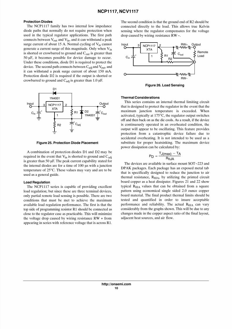
Protection Diodes
The NCP1117 family has two internal low impedance
diode paths that normally do not require protection when
used in the typical regulator applications. The first path
connects between Vout and Vin, and it can withstand a peak
surge current of about 15 A. Normal cycling of Vin cannot
generate a current surge of this magnitude. Only when Vin
is shorted or crowbarred to ground and Cout is greater than
50 F, it becomes possible for device damage to occur.Under these conditions, diode D1 is required to protect the
device. The second path connects between Cadj and Vout, and
it can withstand a peak surge current of about 150 mA.
Protection diode D2 is required if the output is shorted or
crowbarred to ground and Cadj is greater than 1.0 F.
Figure 25. Protection Diode Placement
1
2 Output3Input NCP1117
XTA+ +
CoutCin
R2+
Cadj
R1
1N4001
D1
D2
1N4001
A combination of protection diodes D1 and D2 may be
required in the event that Vin is shorted to ground and Cadj
is greater than 50 F. The peak current capability stated for
the internal diodes are for a time of 100 s with a junction
temperature of 25°C. These values may vary and are to be
used as a general guide.
Load Regulation
The NCP1117 series is capable of providing excellent
load regulation; but since these are three terminal devices,
only partial remote load sensing is possible. There are two
conditions that must be met to achieve the maximum
available load regulation performance. The first is that the
top side of programming resistor R1 should be connected as
close to the regulator case as practicable. This will minimize
the voltage drop caused by wiring resistance RW + from
appearing in series with reference voltage that is across R1.
The second condition is that the ground end of R2 should be
connected directly to the load. This allows true Kelvin
sensing where the regulator compensates for the voltage
drop caused by wiring resistance RW−.
Figure 26. Load Sensing
1
2 Output3Input NCP1117
XTA
+
+Cout
CinR1
Remote
Load
RW+
RW−
R2
Thermal Considerations
This series contains an internal thermal limiting circuit
that is designed to protect the regulator in the event that the
maximum junction temperature is exceeded. When
activated, typically at 175°C, the regulator output switchesoff and then back on as the die cools. As a result, if the device
is continuously operated in an overheated condition, the
output will appear to be oscillating. This feature provides
protection from a catastrophic device failure due to
accidental overheating. It is not intended to be used as a
substitute for proper heatsinking. The maximum device
power dissipation can be calculated by:
PD TJ(max) T A
RJA
The devices are available in surface mount SOT−223 and
DPAK packages. Each package has an exposed metal tab
that is specifically designed to reduce the junction to airthermal resistance, RJA , by utilizing the printed circuit
board copper as a heat dissipater. Figures 21 and 22 show
typical RJA values that can be obtained from a square
pattern using economical single sided 2.0 ounce copper
board material. The final product thermal limits should be
tested and quantified in order to insure acceptable
performance and reliability. The actual RJA can vary
considerably from the graphs shown. This will be due to any
changes made in the copper aspect ratio of the final layout,
adjacent heat sources, and air flow.
8/13/2019 Regulador Voltage 3.3v Xbox360
http://slidepdf.com/reader/full/regulador-voltage-33v-xbox360 11/18
NCP1117, NCV1117
http://onsemi.com
11
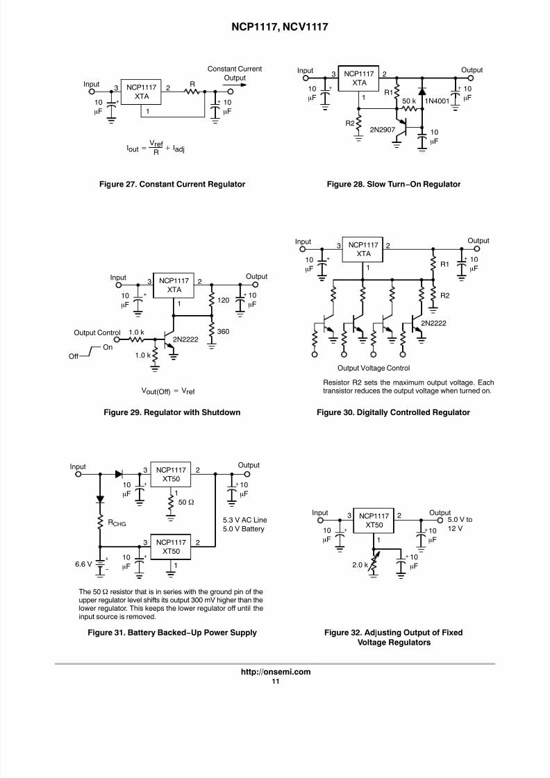
Figure 27. Constant Current Regulator Figure 28. Slow Turn−On Regulator
Figure 29. Regulator with Shutdown Figure 30. Digitally Controlled Regulator
Figure 31. Battery Backed−Up Power Supply Figure 32. Adjusting Output of Fixed
Voltage Regulators
The 50 resistor that is in series with the ground pin of theupper regulator level shifts its output 300 mV higher than thelower regulator. This keeps the lower regulator off until theinput source is removed.
Resistor R2 sets the maximum output voltage. Eachtransistor reduces the output voltage when turned on.
1
2
Constant Current
Output
3Input NCP1117
XTA+ +10
F
IoutVref
R Iadj
10
F
R
1
2Output
3Input NCP1117
XTA+ +10
F
10
F1N4001
R2
R1
10
F
50 k
2N2907
1
2Output
3Input NCP1117
XTA+ +10
F
10
F120
2N2222360
1.0 k
1.0 kOutput Control
On
Off
1
2Output
3Input NCP1117
XTA+ +10
F
10
FR1
2N2222
R2
1
50
2Output
3Input NCP1117
XT50+ +10
F
10
F
+
RCHG
1
NCP1117XT50+10
F−
6.6 V
5.3 V AC Line
5.0 V Battery
1
2 Output3Input NCP1117
XT50+ +10
F
+ 10
F
10
F
2.0 k
5.0 V to
12 V
Vout(Off) Vref
Output Voltage Control
23
8/13/2019 Regulador Voltage 3.3v Xbox360
http://slidepdf.com/reader/full/regulador-voltage-33v-xbox360 12/18
NCP1117, NCV1117
http://onsemi.com
12
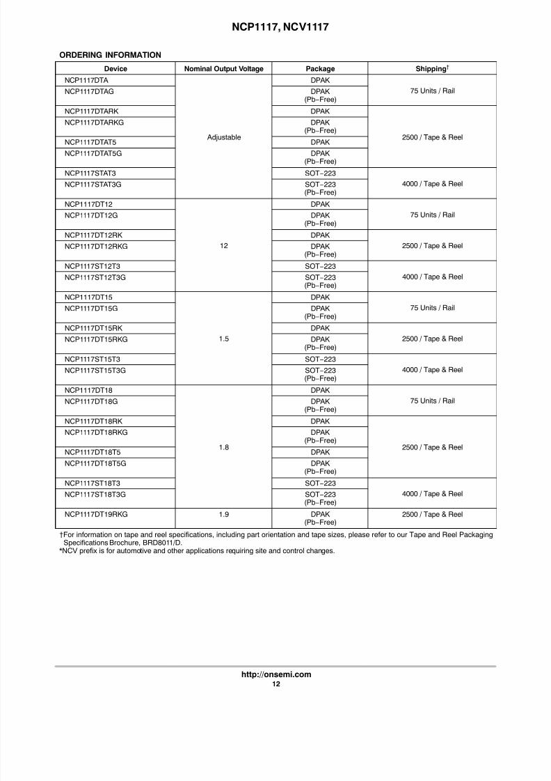
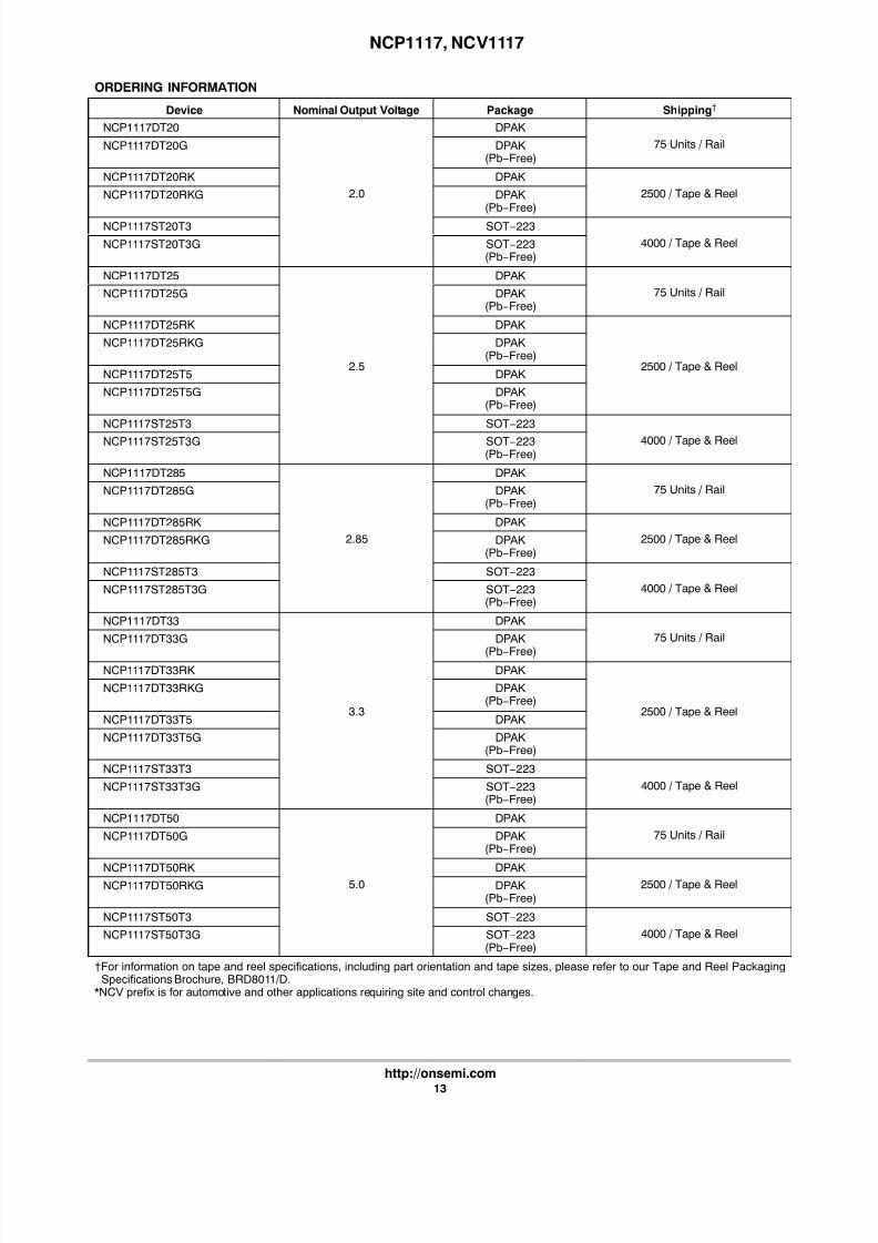
ORDERING INFORMATION
Device Nominal Output Voltage Package Shipping†
NCP1117DTA
Adjustable
DPAK
75 Units / RailNCP1117DTAG DPAK (Pb−Free)
NCP1117DTARK DPAK
2500 / Tape & Reel
NCP1117DTARKG DPAK (Pb−Free)
NCP1117DTAT5 DPAK
NCP1117DTAT5G DPAK (Pb−Free)
NCP1117STAT3 SOT−223
4000 / Tape & ReelNCP1117STAT3G SOT−223(Pb−Free)
NCP1117DT12
12
DPAK
75 Units / RailNCP1117DT12G DPAK (Pb−Free)
NCP1117DT12RK DPAK
2500 / Tape & ReelNCP1117DT12RKG DPAK (Pb−Free)
NCP1117ST12T3 SOT−223
4000 / Tape & ReelNCP1117ST12T3G SOT−
223(Pb−Free)
NCP1117DT15
1.5
DPAK
75 Units / RailNCP1117DT15G DPAK (Pb−Free)
NCP1117DT15RK DPAK
2500 / Tape & ReelNCP1117DT15RKG DPAK (Pb−Free)
NCP1117ST15T3 SOT−223
4000 / Tape & ReelNCP1117ST15T3G SOT−223(Pb−Free)
NCP1117DT18
1.8
DPAK
75 Units / RailNCP1117DT18G DPAK
(Pb−
Free)NCP1117DT18RK DPAK
2500 / Tape & Reel
NCP1117DT18RKG DPAK (Pb−Free)
NCP1117DT18T5 DPAK
NCP1117DT18T5G DPAK (Pb−Free)
NCP1117ST18T3 SOT−223
4000 / Tape & ReelNCP1117ST18T3G SOT−223(Pb−Free)
NCP1117DT19RKG 1.9 DPAK (Pb−Free)
2500 / Tape & Reel
†For information on tape and reel specifications, including part orientation and tape sizes, please refer to our Tape and Reel PackagingSpecifications Brochure, BRD8011/D.
*NCV prefix is for automotive and other applications requiring site and control changes.
8/13/2019 Regulador Voltage 3.3v Xbox360
http://slidepdf.com/reader/full/regulador-voltage-33v-xbox360 13/18
NCP1117, NCV1117
http://onsemi.com
13
ORDERING INFORMATION
Device Shipping†PackageNominal Output Voltage
NCP1117DT20
2.0
DPAK
75 Units / RailNCP1117DT20G DPAK (Pb−Free)
NCP1117DT20RK DPAK
2500 / Tape & ReelNCP1117DT20RKG DPAK (Pb−Free)
NCP1117ST20T3 SOT−223
4000 / Tape & ReelNCP1117ST20T3G SOT−223(Pb−Free)
NCP1117DT25
2.5
DPAK
75 Units / RailNCP1117DT25G DPAK (Pb−Free)
NCP1117DT25RK DPAK
2500 / Tape & Reel
NCP1117DT25RKG DPAK (Pb−Free)
NCP1117DT25T5 DPAK
NCP1117DT25T5G DPAK (Pb−Free)
NCP1117ST25T3 SOT−223
4000 / Tape & ReelNCP1117ST25T3G SOT−
223(Pb−Free)
NCP1117DT285
2.85
DPAK
75 Units / RailNCP1117DT285G DPAK (Pb−Free)
NCP1117DT285RK DPAK
2500 / Tape & ReelNCP1117DT285RKG DPAK (Pb−Free)
NCP1117ST285T3 SOT−223
4000 / Tape & ReelNCP1117ST285T3G SOT−223(Pb−Free)
NCP1117DT33
3.3
DPAK
75 Units / RailNCP1117DT33G DPAK
(Pb−
Free)NCP1117DT33RK DPAK
2500 / Tape & Reel
NCP1117DT33RKG DPAK (Pb−Free)
NCP1117DT33T5 DPAK
NCP1117DT33T5G DPAK (Pb−Free)
NCP1117ST33T3 SOT−223
4000 / Tape & ReelNCP1117ST33T3G SOT−223(Pb−Free)
NCP1117DT50
5.0
DPAK
75 Units / RailNCP1117DT50G DPAK (Pb−Free)
NCP1117DT50RK DPAK 2500 / Tape & ReelNCP1117DT50RKG DPAK
(Pb−Free)
NCP1117ST50T3 SOT−223
4000 / Tape & ReelNCP1117ST50T3G SOT−223(Pb−Free)
†For information on tape and reel specifications, including part orientation and tape sizes, please refer to our Tape and Reel PackagingSpecifications Brochure, BRD8011/D.
*NCV prefix is for automotive and other applications requiring site and control changes.
8/13/2019 Regulador Voltage 3.3v Xbox360
http://slidepdf.com/reader/full/regulador-voltage-33v-xbox360 14/18
NCP1117, NCV1117
http://onsemi.com
14
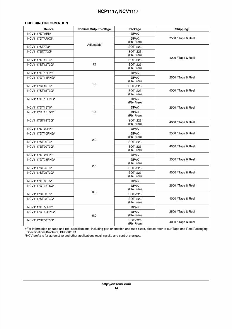
ORDERING INFORMATION
Device Shipping†PackageNominal Output Voltage
NCV1117DTARK*
Adjustable
DPAK
2500 / Tape & ReelNCV1117DTARKG* DPAK (Pb−Free)
NCV1117STAT3* SOT−223
4000 / Tape & Reel
NCV1117STAT3G* SOT−223(Pb−Free)
NCV1117ST12T3*
12
SOT−223
NCV1117ST12T3G* SOT−223(Pb−Free)
NCV1117DT15RK*
1.5
DPAK
2500 / Tape & ReelNCV1117DT15RKG* DPAK (Pb−Free)
NCV1117ST15T3* SOT−223
4000 / Tape & ReelNCV1117ST15T3G* SOT−223(Pb−Free)
NCV1117DT18RKG*
1.8
DPAK (Pb−Free)
2500 / Tape & ReelNCV1117DT18T5* DPAK
NCV1117DT18T5G* DPAK
(Pb−
Free)
NCV1117ST18T3G* SOT−223(Pb−Free)
4000 / Tape & Reel
NCV1117DT20RK*
2.0
DPAK
2500 / Tape & ReelNCV1117DT20RKG* DPAK (Pb−Free)
NCV1117ST20T3* SOT−223
4000 / Tape & ReelNCV1117ST20T3G* SOT−223(Pb−Free)
NCV1117DT25RK*
2.5
DPAK
2500 / Tape & ReelNCV1117DT25RKG* DPAK (Pb−Free)
NCV1117ST25T3* SOT−223
4000 / Tape & ReelNCV1117ST25T3G* SOT−
223(Pb−Free)
NCV1117DT33T5*
3.3
DPAK
2500 / Tape & ReelNCV1117DT33T5G* DPAK (Pb−Free)
NCV1117ST33T3* SOT−223
4000 / Tape & ReelNCV1117ST33T3G* SOT−223(Pb−Free)
NCV1117DT50RK*
5.0
DPAK
2500 / Tape & ReelNCV1117DT50RKG* DPAK (Pb−Free)
NCV1117ST50T3G* SOT−223(Pb−Free)
4000 / Tape & Reel
†For information on tape and reel specifications, including part orientation and tape sizes, please refer to our Tape and Reel PackagingSpecifications Brochure, BRD8011/D.
*NCV prefix is for automotive and other applications requiring site and control changes.
8/13/2019 Regulador Voltage 3.3v Xbox360
http://slidepdf.com/reader/full/regulador-voltage-33v-xbox360 15/18
NCP1117, NCV1117
http://onsemi.com
15
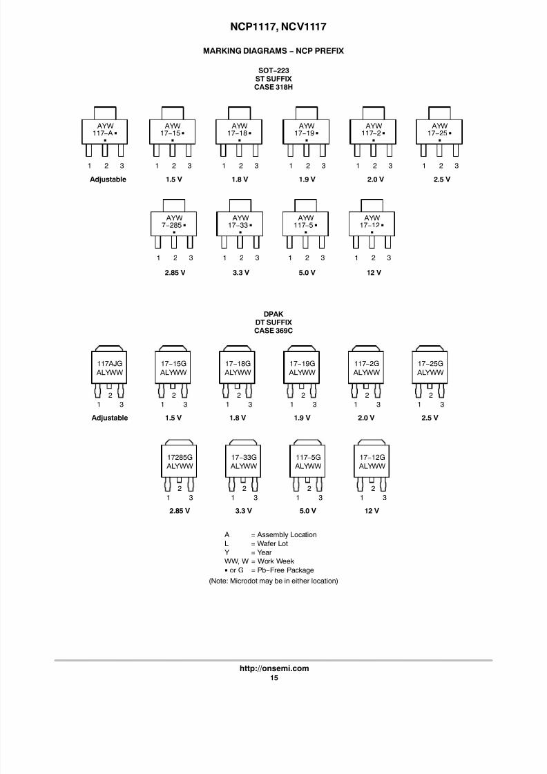
117AJG
ALYWW
17−15G
ALYWW
17−18G
ALYWW
117−2G
ALYWW
17−25G
ALYWW
17285G
ALYWW
17−33G
ALYWW
117−5G
ALYWW
17−12G
ALYWW
AYW
117−
A
1
SOT−223ST SUFFIX CASE 318H
A = Assembly Location
L = Wafer Lot Y = Year
WW, W = Work Week
or G = Pb−Free Package
MARKING DIAGRAMS − NCP PREFIX
DPAK DT SUFFIX CASE 369C
2 3
1
2
3 1
2
3 1
2
3 1
2
3 1
2
3
1
2
3 1
2
3 1
2
3 1
2
3
Adjustable 1.5 V 1.8 V 2.0 V 2.5 V
2.85 V 3.3 V 5.0 V 12 V
Adjustable 1.5 V 1.8 V 2.0 V 2.5 V
2.85 V 3.3 V 5.0 V 12 V
(Note: Microdot may be in either location)
AYW
17−
15
1 2 3
AYW
17−
18
1 2 3
AYW
117−
2
1 2 3
AYW
17−
25
1 2 3
AYW7−285
1 2 3
AYW17−33
1 2 3
AYW117−5
1 2 3
AYW17−12
1 2 3
1.9 V
AYW
17−
19
1 2 3
17−19G
ALYWW
1
2
31.9 V
8/13/2019 Regulador Voltage 3.3v Xbox360
http://slidepdf.com/reader/full/regulador-voltage-33v-xbox360 16/18
NCP1117, NCV1117
http://onsemi.com
16
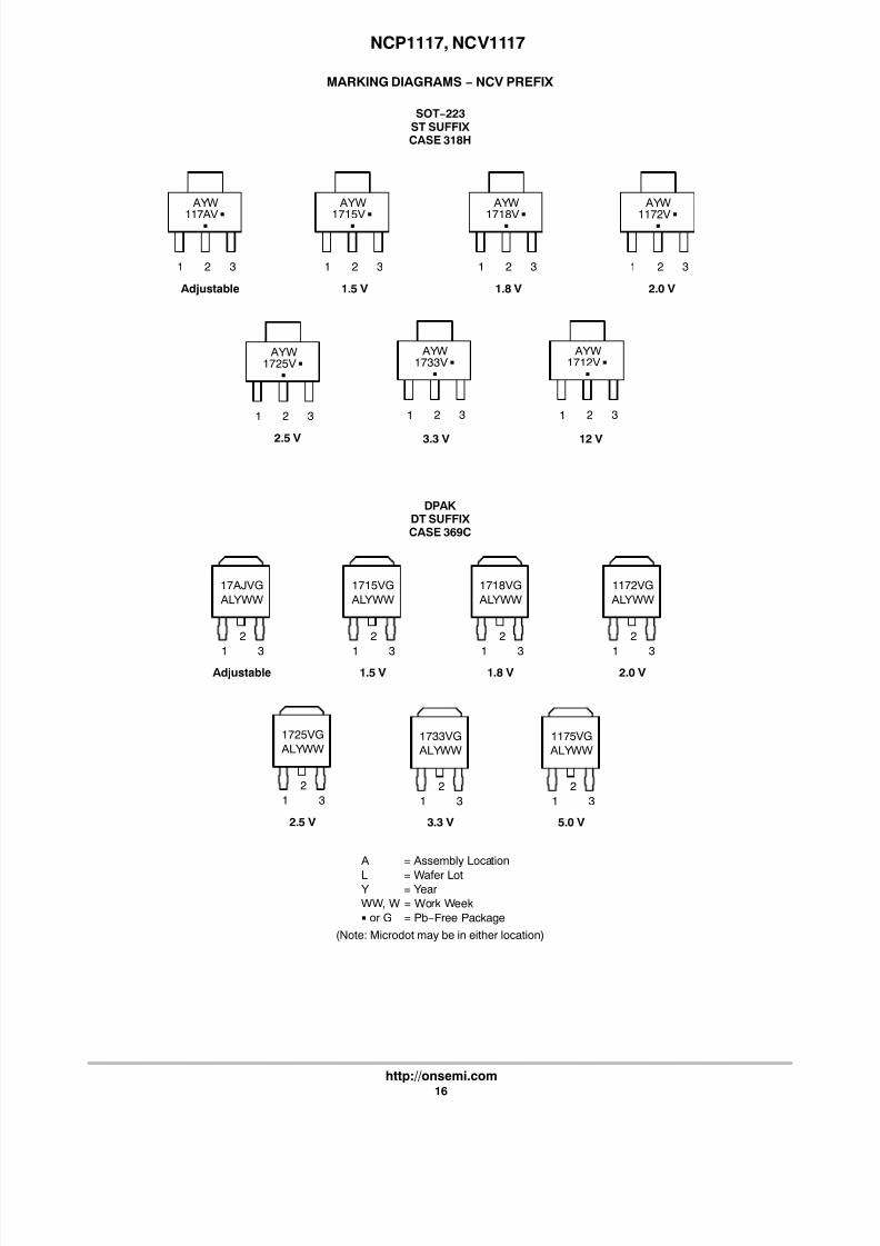
17AJVG
ALYWW
1715VG
ALYWW
1718VG
ALYWW
1172VG
ALYWW
1725VG
ALYWW1733VG
ALYWW
1175VG
ALYWW
AYW
117AV
1
SOT−223ST SUFFIX CASE 318H
A = Assembly Location
L = Wafer Lot Y = Year
WW, W = Work Week
or G = Pb−Free Package
MARKING DIAGRAMS − NCV PREFIX
DPAK DT SUFFIX CASE 369C
2 3
1
2
3 1
2
3 1
2
3 1
2
3
1
2
3 1
2
3 1
2
3
Adjustable 1.5 V 2.0 V
2.5 V 3.3 V 12 V
Adjustable 1.5 V 1.8 V 2.0 V
2.5 V 3.3 V 5.0 V
(Note: Microdot may be in either location)
AYW
1715V
1 2 3
AYW
1172V
1 2 3
AYW1725V
1 2 3
AYW1733V
1 2 3
AYW1712V
1 2 3
1.8 V
AYW
1718V
1 2 3
8/13/2019 Regulador Voltage 3.3v Xbox360
http://slidepdf.com/reader/full/regulador-voltage-33v-xbox360 17/18
NCP1117, NCV1117
http://onsemi.com
17
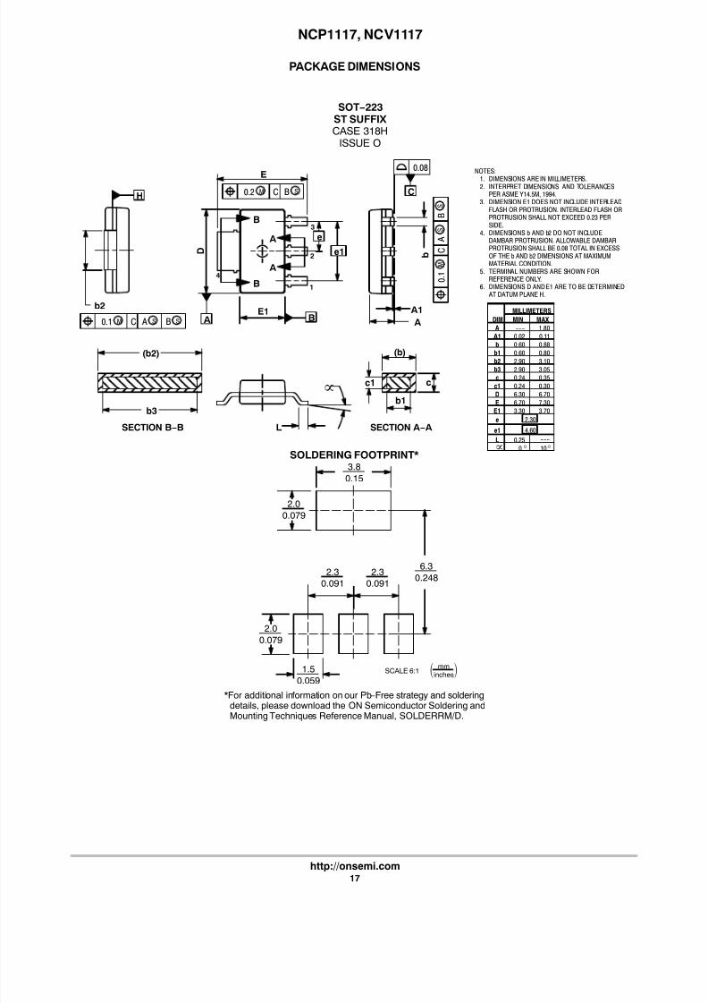
PACKAGE DIMENSIONS
SOT−223ST SUFFIX CASE 318H
ISSUE O
É É É
É É É
NOTES:1. DIMENSIONS ARE IN MILLIMETERS.2. INTERPRET DIMENSIONS AND TOLERANCES
PER ASME Y14.5M, 1994.3. DIMENSION E1 DOES NOT INCLUDE INTERLEAD
FLASH OR PROTRUSION. INTERLEAD FLASH ORPROTRUSION SHALL NOT EXCEED 0.23 PERSIDE.
4. DIMENSIONS b AND b2 DO NOT INCLUDEDAMBAR PROTRUSION. ALLOWABLE DAMBARPROTRUSION SHALL BE 0.08 TOTAL IN EXCESSOF THE b AND b2 DIMENSIONS AT MAXIMUMMATERIAL CONDITION.
5. TERMINAL NUMBERS ARE SHOWN FORREFERENCE ONLY.
6. DIMENSIONS D AND E1 ARE TO BE DETERMINED AT DATUM PLANE H.
DIM MIN MAX
MILLIMETERS
A --- 1.80
A1 0.02 0.11
b 0.60 0.88
b1 0.60 0.80b2 2.90 3.10
b3 2.90 3.05
c 0.24 0.35
c1 0.24 0.30
D 6.30 6.70
E 6.70 7.30
E1 3.30 3.70
e 2.30
e1 4.60
L 0.25 ---
0 10
c1
E
HM0.2 C C
A
SB
B
B
A
A
M
0 . 1
C
S
A
S
B
E1B
D
4
3
2
1
e
e1
M0.1 C S A SB
b2
b
A
0.08
A1
c
b1
(b)(b2)
b3
SECTION B−B L
Ç Ç Ç
Ç Ç Ç
É É É É É É É
É É É É É É É
Ç Ç Ç Ç Ç Ç Ç
Ç Ç Ç Ç Ç Ç Ç
SECTION A−A
1.5
0.059
mminchesSCALE 6:1
3.8
0.15
2.0
0.079
6.3
0.2482.3
0.091
2.3
0.091
2.0
0.079
*For additional information on our Pb−Free strategy and soldering
details, please download the ON Semiconductor Soldering andMounting Techniques Reference Manual, SOLDERRM/D.
SOLDERING FOOTPRINT*
8/13/2019 Regulador Voltage 3.3v Xbox360
http://slidepdf.com/reader/full/regulador-voltage-33v-xbox360 18/18
NCP1117, NCV1117
http://onsemi com
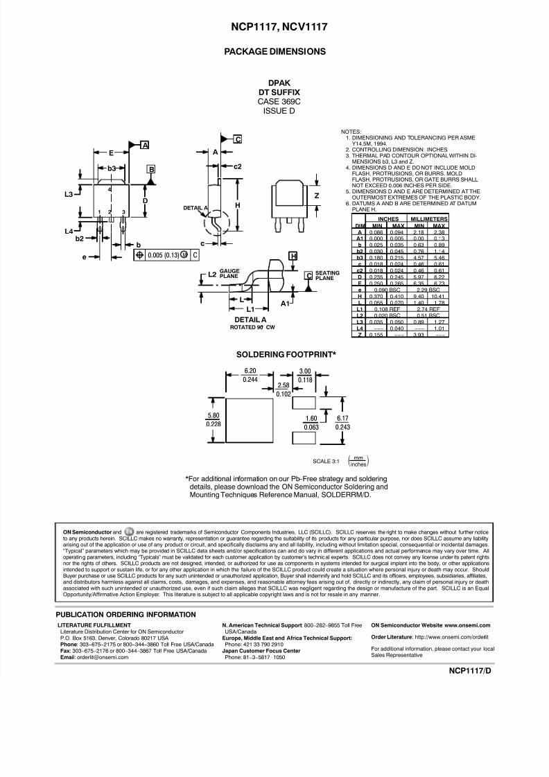
PACKAGE DIMENSIONS
DPAK DT SUFFIX CASE 369C
ISSUE D
b
D
E
b3
L3
L4b2
e M0.005 (0.13) C
c2
A
c
C
Z
DIM MIN MAX MIN MAX
MILLIMETERSINCHES
D 0.235 0.245 5.97 6.22E 0.250 0.265 6.35 6.73
A 0.086 0.094 2.18 2.38
b 0.025 0.035 0.63 0.89
c2 0.018 0.024 0.46 0.61
b2 0.030 0.045 0.76 1.14
c 0.018 0.024 0.46 0.61
e 0.090 BSC 2.29 BSC
b3 0.180 0.215 4.57 5.46
L4 −−− 0.040 −−− 1.01
L 0.055 0.070 1.40 1.78
L3 0.035 0.050 0.89 1.27
Z 0.155 −−− 3.93 −−−
NOTES:
1. DIMENSIONING AND TOLERANCING PER ASME Y14.5M, 1994.
2. CONTROLLING DIMENSION: INCHES.3. THERMAL PAD CONTOUR OPTIONAL WITHIN DI-
MENSIONS b3, L3 and Z.4. DIMENSIONS D AND E DO NOT INCLUDE MOLD
FLASH, PROTRUSIONS, OR BURRS. MOLDFLASH, PROTRUSIONS, OR GATE BURRS SHALLNOT EXCEED 0.006 INCHES PER SIDE.
5. DIMENSIONS D AND E ARE DETERMINED AT THEOUTERMOST EXTREMES OF THE PLASTIC BODY.
6. DATUMS A AND B ARE DETERMINED AT DATUMPLANE H.1 2 3
4
5.80
0.228
2.58
0.102
1.60
0.063
6.20
0.244
3.00
0.118
6.17
0.243
mm
inchesSCALE 3:1
*For additional information on our Pb−Free strategy and solderingdetails, please download the ON Semiconductor Soldering andMounting Techniques Reference Manual, SOLDERRM/D.
SOLDERING FOOTPRINT*
H 0.370 0.410 9.40 10.41
A1 0.000 0.005 0.00 0.13
L1 0.108 REF 2.74 REFL2 0.020 BSC 0.51 BSC
A1
HDETAIL A
SEATINGPLANE
A
B
C
L1
L
H
L2 GAUGEPLANE
DETAIL AROTATED 90 CW
ON Semiconductor and are registered trademarks of Semiconductor Components Industries, LLC (SCILLC). SCILLC reserves the right to make changes without further noticeto any products herein. SCILLC makes no warranty, representation or guarantee regarding the suitability of its products for any particular purpose, nor does SCILLC assume any liability
arising out of the application or use of any product or circuit, and specifically disclaims any and all liability, including without limitation special, consequential or incidental damages.“Typical” parameters which may be provided in SCILLC data sheets and/or specifications can and do vary in different applications and actual performance may vary over time. Alloperating parameters, including “Typicals” must be validated for each customer application by customer’s technical experts. SCILLC does not convey any license under its patent rightsnor the rights of others. SCILLC products are not designed, intended, or authorized for use as components in systems intended for surgical implant into the body, or other applicationsintended to support or sustain life, or for any other application in which the failure of the SCILLC product could create a situation where personal injury or death may occur. ShouldBuyer purchase or use SCILLC products for any such unintended or unauthorized application, Buyer shall indemnify and hold SCILLC and its officers, employees, subsidiaries, affiliates,and distributors harmless against all claims, costs, damages, and expenses, and reasonable attorney fees arising out of, directly or indirectly, any claim of personal injury or deathassociated with such unintended or unauthorized use, even if such claim alleges that SCILLC was negligent regarding the design or manufacture of the part. SCILLC is an EqualOpportunity/Affirmative Action Employer. This literature is subject to all applicable copyright laws and is not for resale in any manner.
NCP1117/D
PUBLICATION ORDERING INFORMATION
N. American Technical Support: 800−282−9855 Toll FreeUSA/Canada
Europe, Middle East and Africa Technical Support:Phone: 421 33 790 2910
Japan Customer Focus CenterPhone: 81−3−5817−1050
LITERATURE FULFILLMENT:Literature Distribution Center for ON SemiconductorP.O. Box 5163, Denver, Colorado 80217 USAPhone: 303−675−2175 or 800−344−3860 Toll Free USA/CanadaFax : 303−675−2176 or 800−344−3867 Toll Free USA/CanadaEmail: [email protected]
ON Semiconductor Website: www.onsemi.com
Order Literature: http://www.onsemi.com/orderlit
For additional information, please contact your localSales Representative