Embed Size (px)
Citation preview
6.012 - Microelectronic Devices and Circuits - Fall 2005 Lecture 18-1
Lecture 18 - The Bipolar Junction Transistor(II)
Regimes of Operation
November 10, 2005
Contents:
1. Regimes of operation.
2. Large-signal equivalent circuit model.
3. Output characteristics.
Reading assignment:
Howe and Sodini, Ch. 7, §§7.3, 7.4
Announcements:
Quiz 2: 11/16, 7:30-9:30 PM,open book, must bring calculator; lectures #10-18.
6.012 - Microelectronic Devices and Circuits - Fall 2005 Lecture 18-2
Key questions
• What other regimes of operation are there for the BJT?
• What is unique about each regime?
• How do equivalent circuit models for the BJT look like?
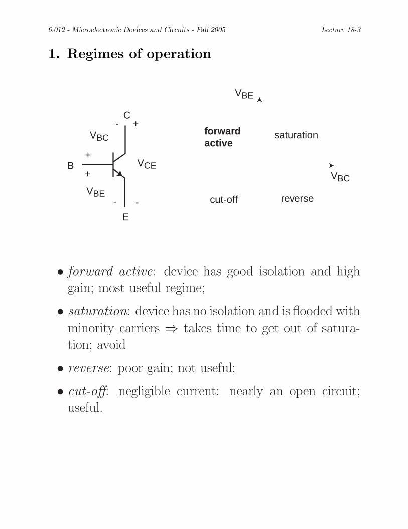
6.012 - Microelectronic Devices and Circuits - Fall 2005 Lecture 18-3
1. Regimes of operation
VBE
C- +
VBC forward saturation active
+B VCE
+ VBC
VBE reverse - - cut-off
E
• forward active: device has good isolation and high gain; most useful regime;
• saturation: device has no isolation and is flooded with minority carriers ⇒ takes time to get out of satura-tion; avoid
• reverse: poor gain; not useful;
• cut-off: negligible current: nearly an open circuit; useful.

6.012 - Microelectronic Devices and Circuits - Fall 2005 Lecture 18-4
2 Forward-active regime: VBE > 0, VBC < 0
n-Emitter p-Base n-Collector
IE<0
IB>0
IC>0
VBE > 0 VBC < 0
Minority carrier profiles (not to scale):
emitter base collector
npBpnE pnC
npBopnEo
pnCo
x
-WE-XBE -XBE 0 WB WB+XBC WB+XBC+WC
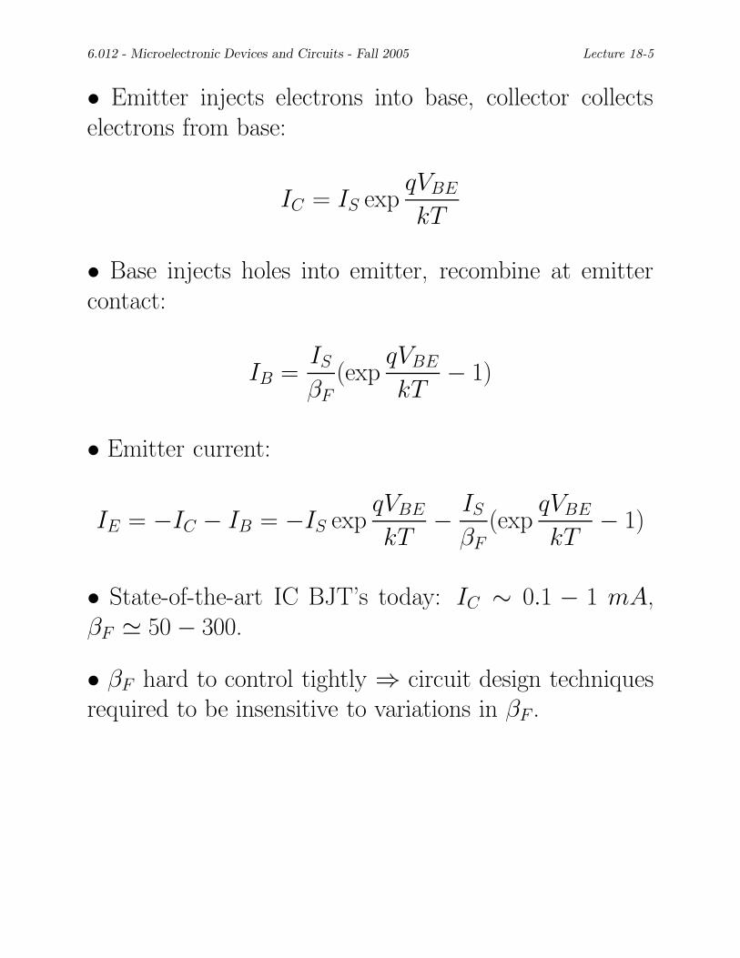
6.012 - Microelectronic Devices and Circuits - Fall 2005 Lecture 18-5
• Emitter injects electrons into base, collector collects electrons from base:
qVBEIC = IS exp
kT
• Base injects holes into emitter, recombine at emitter contact:
IS qVBEIB = (exp − 1)
βF kT
• Emitter current:
qVBE IS qVBEIE = −IC − IB = −IS exp − (exp − 1)
kT βF kT
• State-of-the-art IC BJT’s today: IC ∼ 0.1 − 1 mA, βF � 50 − 300.
• βF hard to control tightly ⇒ circuit design techniques required to be insensitive to variations in βF .
6.012 - Microelectronic Devices and Circuits - Fall 2005 Lecture 18-6
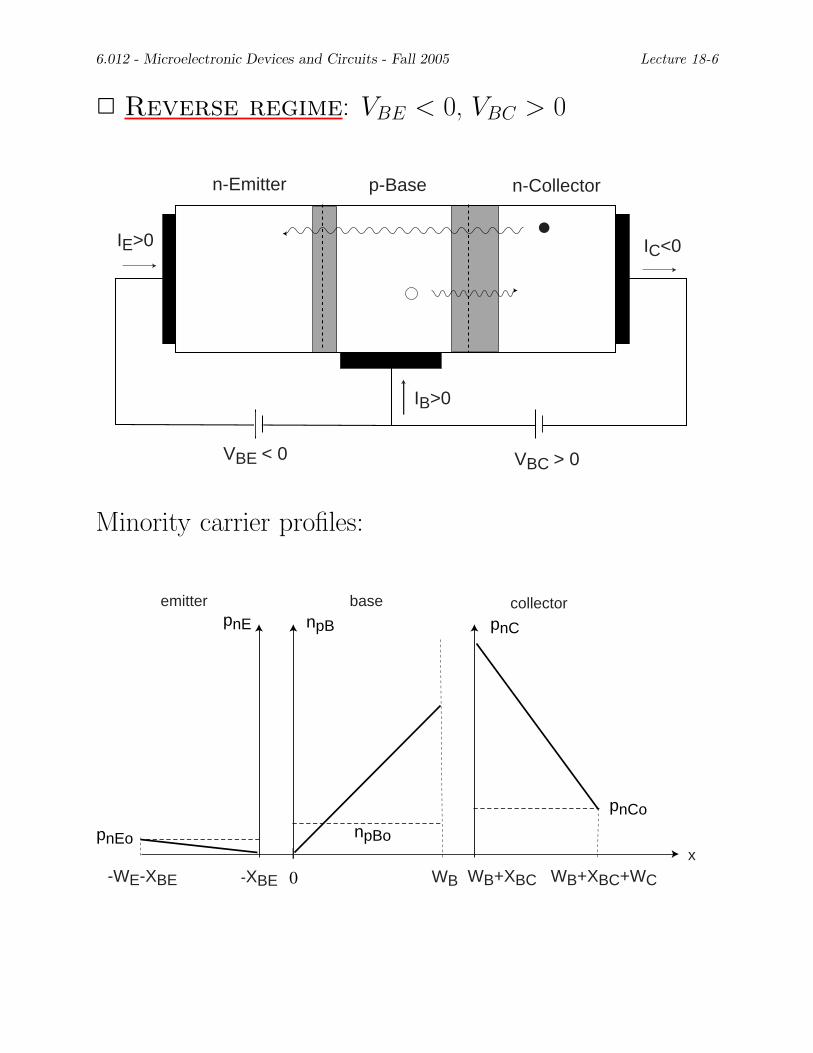
2 Reverse regime: VBE < 0, VBC > 0
n-Emitter p-Base n-Collector
IE>0
IB>0
IC<0
VBE < 0 VBC > 0
Minority carrier profiles:
emitter base collector npBpnE pnC
npBopnEo
pnCo
x -WE-XBE -XBE 0 WB WB+XBC WB+XBC+WC

6.012 - Microelectronic Devices and Circuits - Fall 2005 Lecture 18-7
• Collector injects electrons into base, emitter collects electrons from base:
IE = IS exp qVBC
kT
• Base injects holes into collector, recombine at collector contact and buried layer:
IB = IS
βR (exp
qVBC
kT − 1)
• Collector current:
IC = −IE − IB = −IS exp qVBC
kT −
IS
βR (exp
qVBC
kT − 1)
• Typically, βR � 0.1 − 5 � βF .
IB AC
EB B
IE AE
EB B
C C
6.012 - Microelectronic Devices and Circuits - Fall 2005 Lecture 18-8
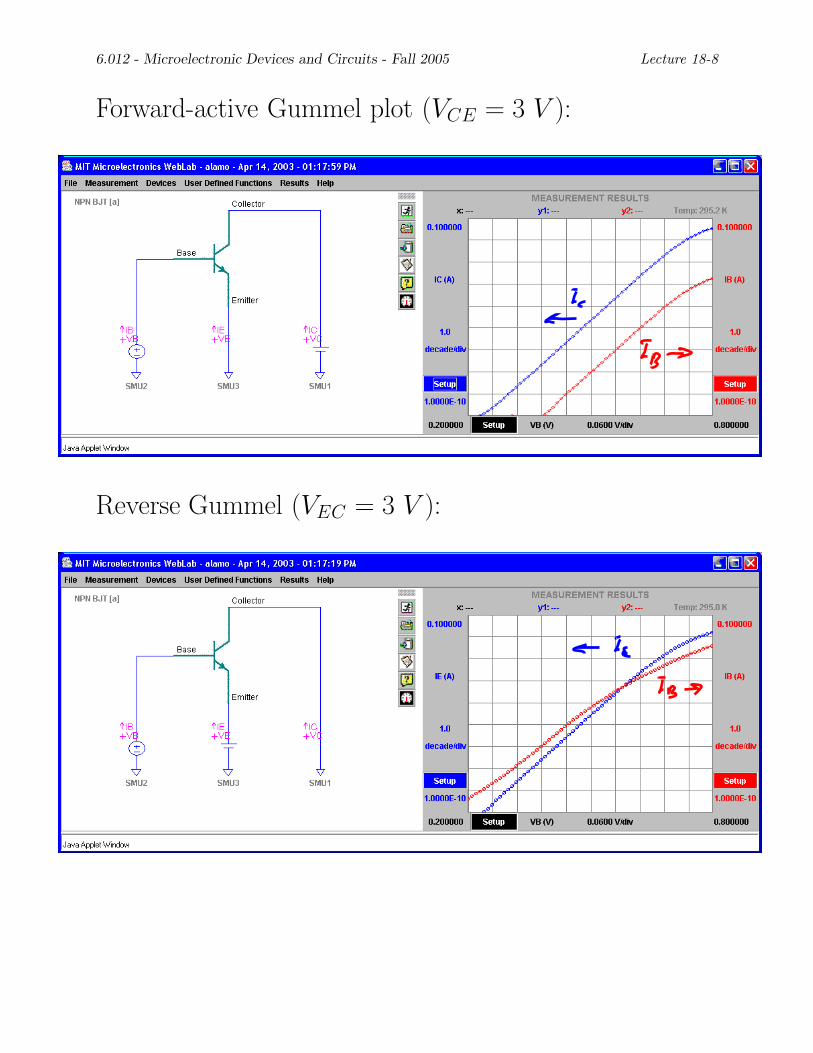
Forward-active Gummel plot (VCE = 3 V ):
Reverse Gummel (VEC = 3 V ):
6.012 - Microelectronic Devices and Circuits - Fall 2005 Lecture 18-9
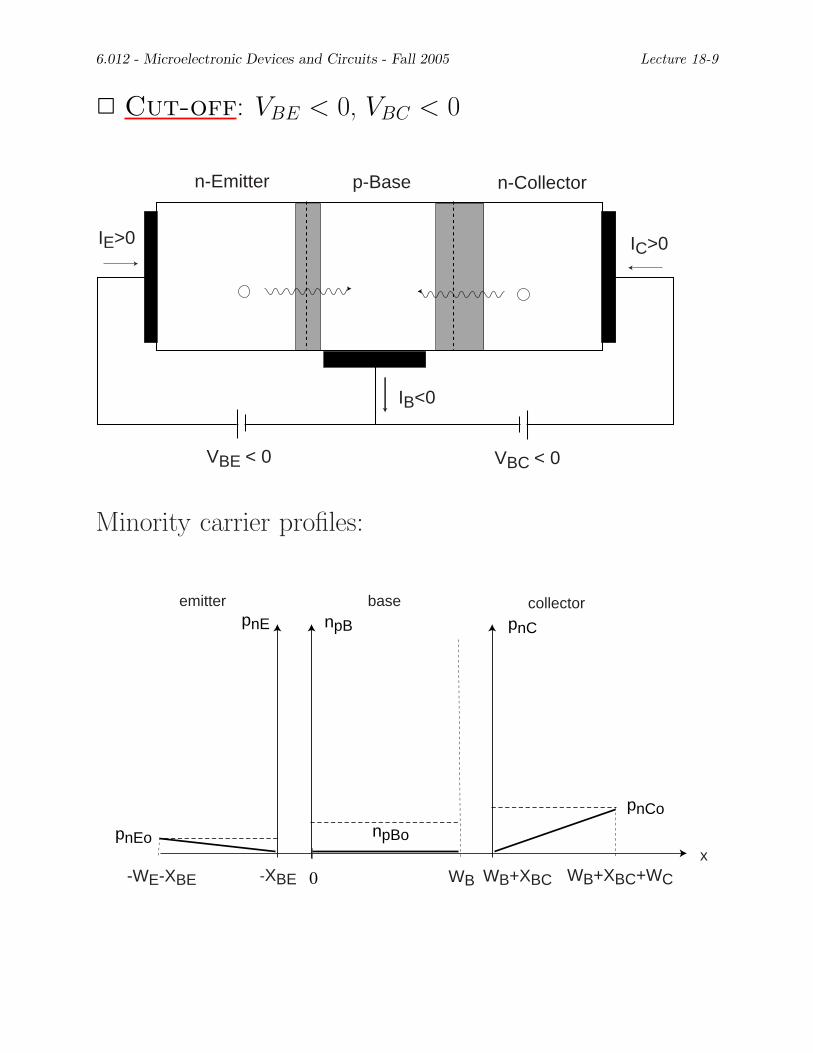
2 Cut-off: VBE < 0, VBC < 0
n-Emitter p-Base n-Collector
IE>0
IB<0
IC>0
VBE < 0 VBC < 0
Minority carrier profiles:
emitter base collector npBpnE pnC
npBopnEo
pnCo
x -WE-XBE -XBE 0 WB WB+XBC WB+XBC+WC
6.012 - Microelectronic Devices and Circuits - Fall 2005 Lecture 18-10
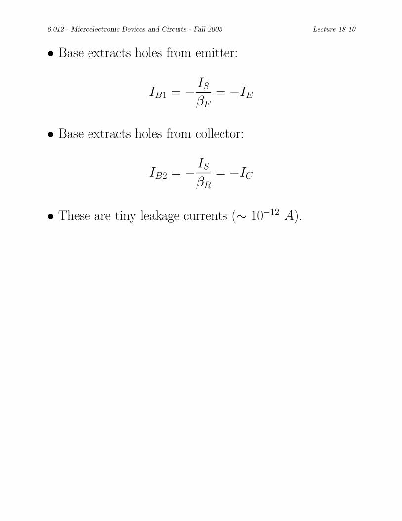
• Base extracts holes from emitter:
ISIB1 = − = −IE
βF
• Base extracts holes from collector:
ISIB2 = − = −IC
βR
• These are tiny leakage currents (∼ 10−12 A).
6.012 - Microelectronic Devices and Circuits - Fall 2005 Lecture 18-11
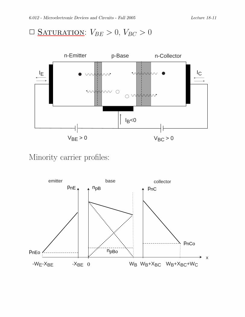
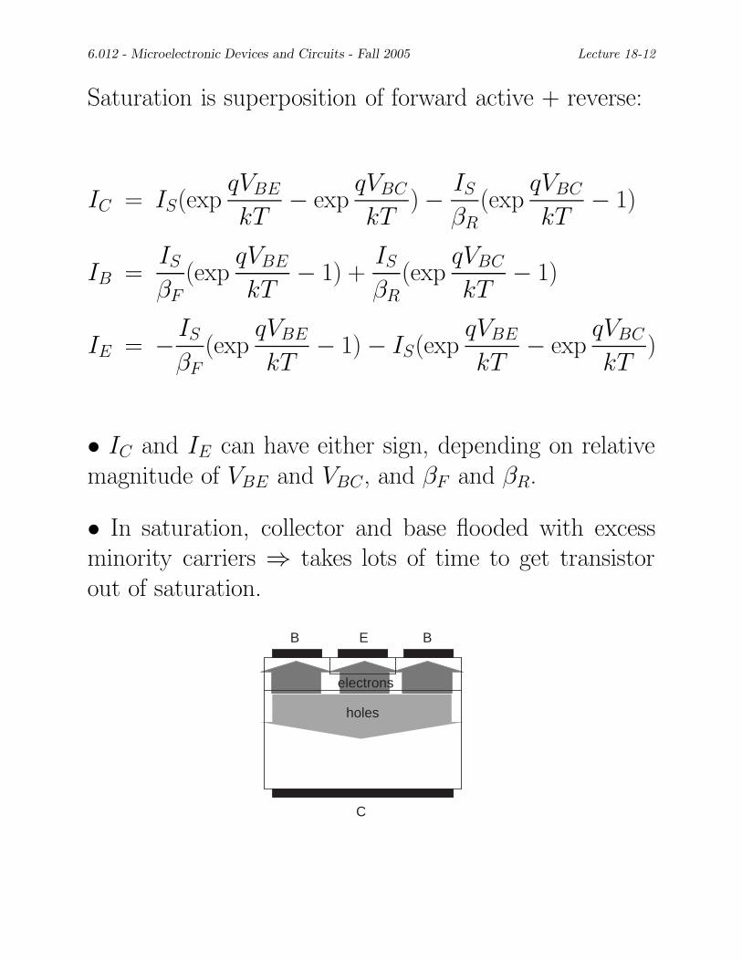
2 Saturation: VBE > 0, VBC > 0
n-Emitter p-Base n-Collector
IE
IB<0
IC
VBE > 0 VBC > 0
Minority carrier profiles:
emitter base collector npBpnE pnC
npBopnEo
pnCo
x -WE-XBE -XBE 0 WB WB+XBC WB+XBC+WC
6.012 - Microelectronic Devices and Circuits - Fall 2005 Lecture 18-12
Saturation is superposition of forward active + reverse:
qVBE qVBC IS qVBCIC = IS(exp − exp ) − (exp − 1)
kT kT βR kT
IS qVBE IS qVBCIB = (exp − 1) + (exp − 1)
βF kT βR kT
IS qVBE qVBE qVBCIE = − (exp − 1) − IS (exp − exp )
βF kT kT kT
• IC and IE can have either sign, depending on relative magnitude of VBE and VBC , and βF and βR.
• In saturation, collector and base flooded with excess minority carriers ⇒ takes lots of time to get transistor out of saturation.
EB B
holes
electrons
C
ar del
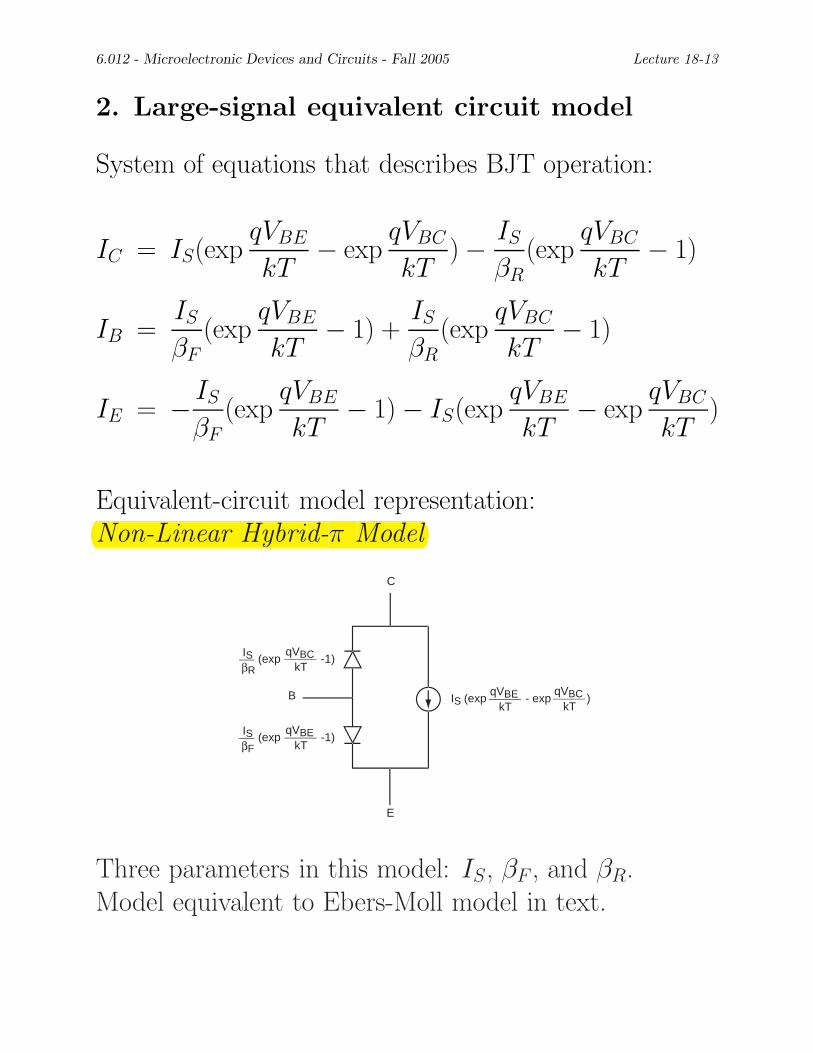
6.012 - Microelectronic Devices and Circuits - Fall 2005 Lecture 18-13
2. Large-signal equivalent circuit model
System of equations that describes BJT operation:
IC = IS(exp qVBE
kT − exp
qVBC
kT ) −
IS
βR (exp
qVBC
kT − 1)
IB = IS
βF (exp
qVBE
kT − 1) +
IS
βR (exp
qVBC
kT − 1)
IE = − IS
βF (exp
qVBE
kT − 1) − IS (exp
qVBE
kT − exp
qVBC
kT )
Equivalent-circuit model representation: Non-Line Hybrid-π MoNon-Linear Hybrid-π Model
C
IS β
IS β
R
F
(exp
(exp
B
qVBE kT
-1)
qVBC kT
-1)
IS (exp qVBE - exp
qVBC )kT kT
E
Three parameters in this model: IS , βF , and βR. Model equivalent to Ebers-Moll model in text.
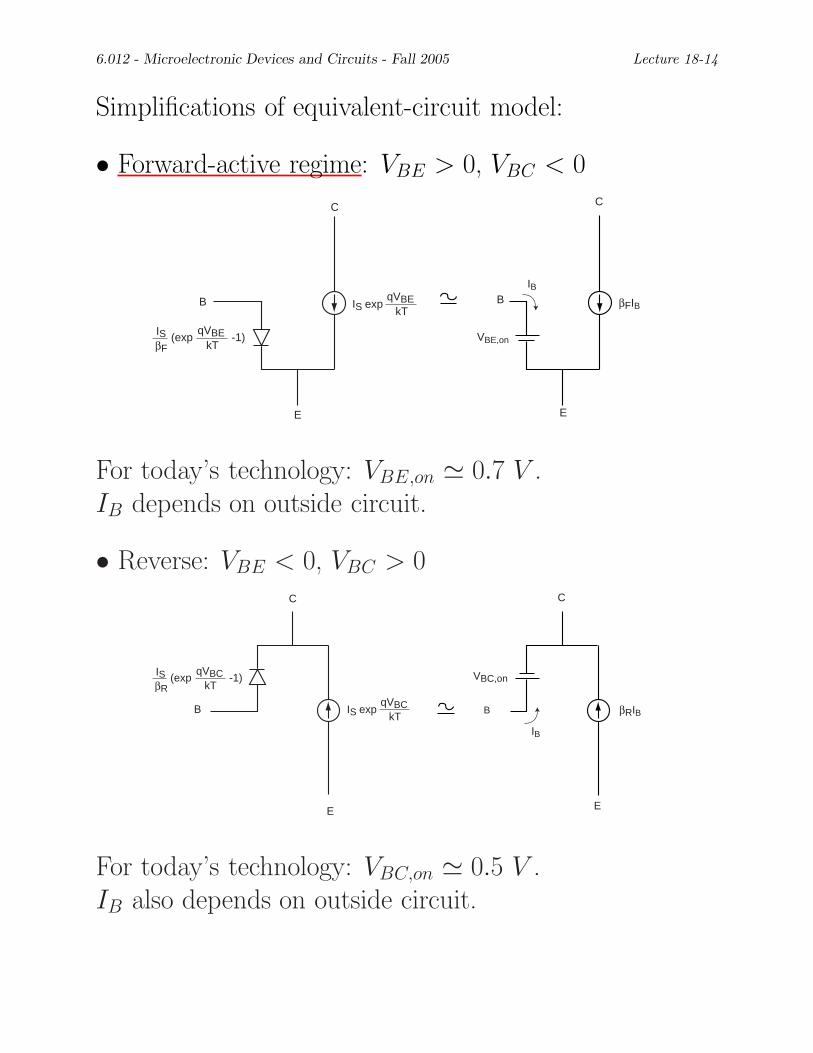
6.012 - Microelectronic Devices and Circuits - Fall 2005 Lecture 18-14
Simplifications of equivalent-circuit model:
• Forward-active regime: VBE > 0, VBC < 0 CC
IB qVBE BB IS exp βFIBkT
IS (exp qVBE -1) VBE,onβF kT
E E
For today’s technology: VBE,on � 0.7 V . IB depends on outside circuit.
• Reverse: VBE < 0, VBC > 0 C C
IS (exp qVBC -1) VBC,on
βR kT
qVBCB IS exp B βRIBkT IB
EE
For today’s technology: VBC,on � 0.5 V . IB also depends on outside circuit.
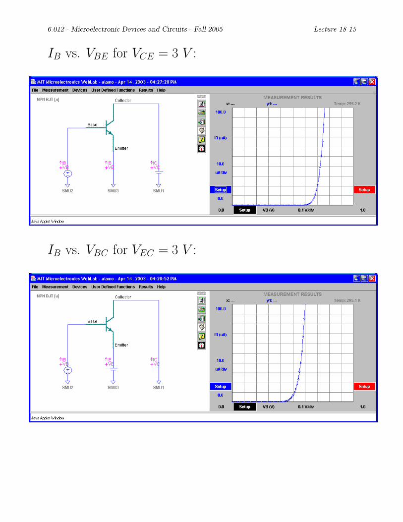
6.012 - Microelectronic Devices and Circuits - Fall 2005 Lecture 18-15
IB vs. VBE for VCE = 3 V :
IB vs. VBC for VEC = 3 V :

6.012 - Microelectronic Devices and Circuits - Fall 2005 Lecture 18-16
• Saturation: VBE > 0, VBC > 0
C C C
+
VBC,on VBC,on
B BB VCE,sat
VBE,on VBE,on
-
E E E
Today’s technology: VCE,sat = VBE,on − VBC,on � 0.2 V . IB and IC depend on outside circuit.
• Cut-off: VBE < 0, VBC < 0
C
B
E
Only negligible leakage currents.
6.012 - Microelectronic Devices and Circuits - Fall 2005 Lecture 18-17
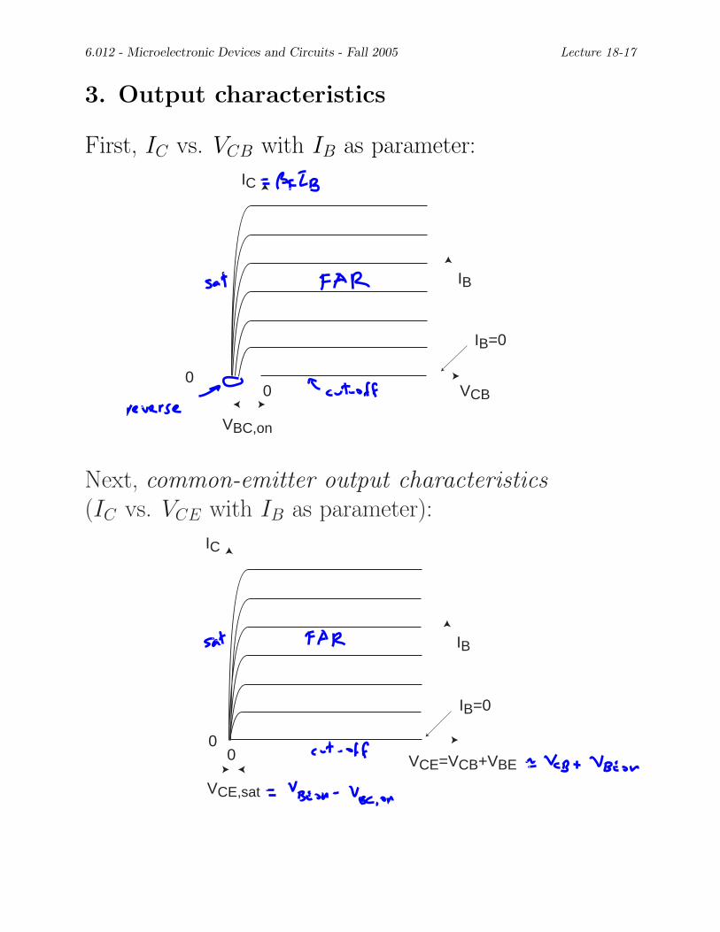
3. Output characteristics
First, IC vs. VCB with IB as parameter:
VCB
VBC,on
IC
IB
IB=0
0 0
Next, common-emitter output characteristics (IC vs. VCE with IB as parameter):
VCE=VCB+VBE
VCE,sat
IC
IB
IB=0
0 0
6.012 - Microelectronic Devices and Circuits - Fall 2005 Lecture 18-18
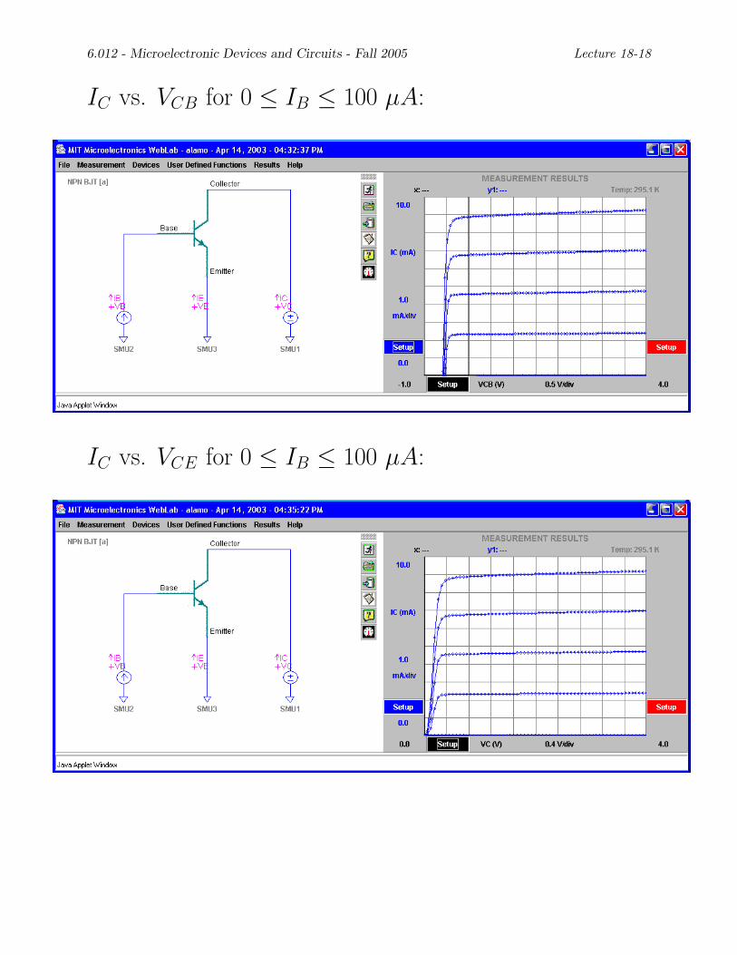
IC vs. VCB for 0 ≤ IB ≤ 100 µA:
IC vs. VCE for 0 ≤ IB ≤ 100 µA:
6.012 - Microelectronic Devices and Circuits - Fall 2005 Lecture 18-19
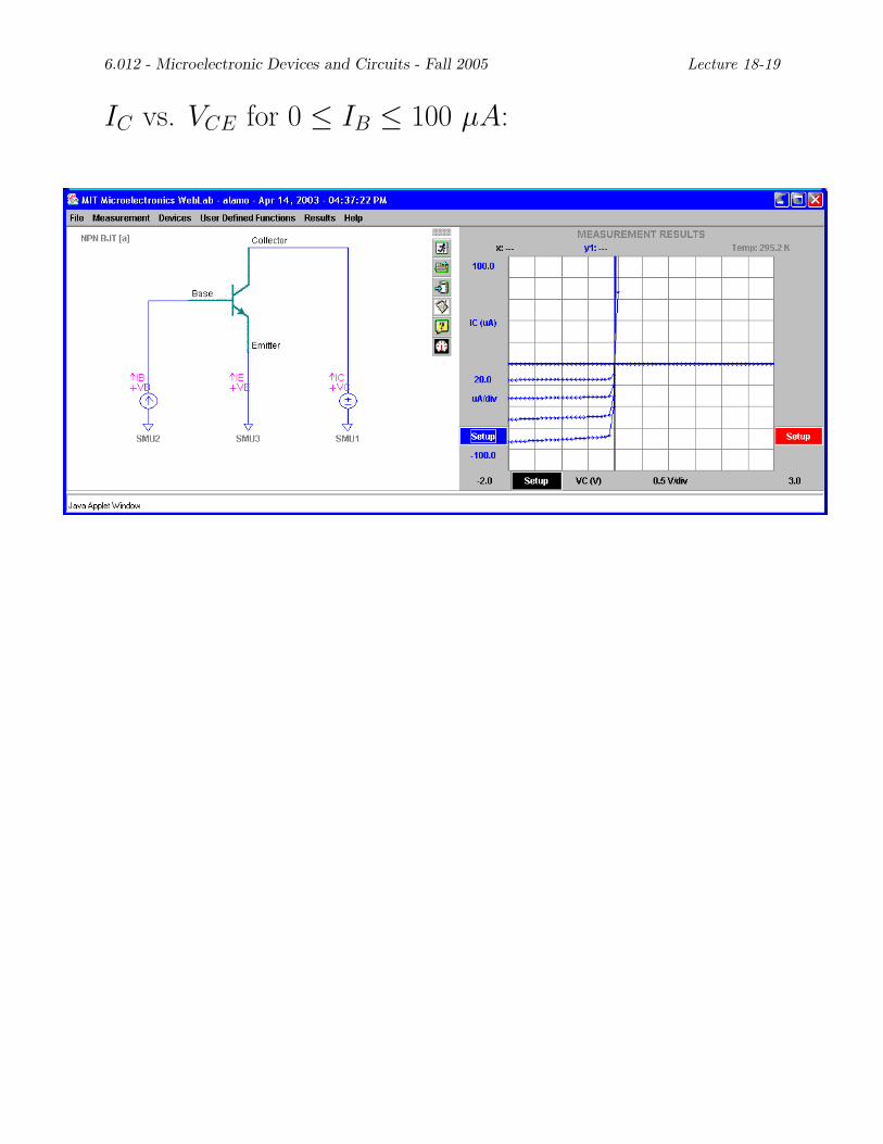
IC vs. VCE for 0 ≤ IB ≤ 100 µA:
6.012 - Microelectronic Devices and Circuits - Fall 2005 Lecture 18-20
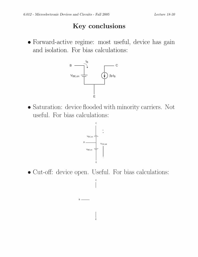
Key conclusions
• Forward-active regime: most useful, device has gain and isolation. For bias calculations:
B C
E
VBE,on
IB
βFIB
• Saturation: device flooded with minority carriers. Not useful. For bias calculations:
C
+
VBC,on
B VCE,sat
VBE,on
-
E
• Cut-off: device open. Useful. For bias calculations:C
B
E