Embed Size (px)
Citation preview
Reduction of Stray Inductance in Power Electronic Modules Using Basic Switching Cells
Shengnan Li1 Student Member, IEEE
Leon M. Tolbert1 Senior Member, IEEE
Fred Wang1 Fellow, IEEE
Fang Zheng Peng2 Fellow, IEEE
1Department of Electrical Engineering and Computer Science, The University of Tennessee, Knoxville, TN, 37996-2100, USA 2Department of Electrical and Computer Engineering, Michigan State University, East Lansing, 48824, USA
Abstract –This paper introduces the concepts of two basic switching cells, P-cell and N-cell, along with their implications in power electronic circuits. The basic switching cells exist in almost every power electronic circuit. To take advantage of these structures, this paper proposes a novel packaging method for power electronics modules. The proposed packaging method uses the basic switching cells as the unit in a module, instead of traditional anti-parallel connection of active switch and diode. This rearrangement can reduce the stray inductance in the current commutation pass; therefore, the performance and reliability of the power device module and the power electronic system can be improved. A conventional phase leg module and a proposed module are modeled. Electromagnetic simulation is carried out to extract the stray inductance from the two modules. Switching behavior under different package parasitics is studied based on Saber simulation.
Index Terms—N-cell, P-cell, package, IGBT module, stray inductance, wire-bond.
I. INTRODUCTION Power electronic modules constitute one of the driving forces towards modularization and integration of power electronic systems [1]. It improves the system performance by greatly reducing the package parasitic impedances. During the past several years, power device and module packaging technology has evolved through multiple generations, each with incremental improvements in performance and reliability. As a result of technology advances that have produced devices with rugged switching characteristics, low losses, and simple gate drive, the insulated gate bipolar transistor (IGBT) has become the device of choice for a wide range of industrial power conversion applications. This paper discusses the module package technology based on IGBT, but it is also applicable to other power electronic devices.
Commercial IGBT power modules include single phase leg and three phase inverter (six pack), which utilize two or six pairs of anti-paralleled IGBTs and free wheel diodes. The packaging technology is mainly based on wire-bond technology. Stray inductance is a major concern in the design and layout of IGBT packages and power stages with both high switching speed and high power handling requirements.
For example, voltage spikes during turn-off transition of the IGBT are proportional to the total loop inductance. The dominant stray inductance inside the package mainly comes from the terminal leads [2]. The most significant improvement, "U-Package" technology developed by Mitsubishi in 1996 [3], was made possible by molding wide electrodes into the sides of the case to form parallel plate structures, which have considerably less inductance than conventional electrodes. Another part of the stray inductance is introduced by the wire-bond connection between the dies and terminal leads. Although it is not a large value, at high current values, inductance of a few nH can make a significant difference.
One of the main objectives in the design of the novel package in this paper is a reduction in internal stray inductance. The introduction of P-cell and N-cell, which are the series connection of active switch and diode, differs from the traditional way of integration and packaging of power devices. This reduces the length of the current pass between active switch and corresponding freewheel diode, and therefore reduces the stray inductance caused by the internal connection bus. Another objective of the proposed package is to reduce the dead time requirement in a phase leg structure by adding inductance between two switching cells.
II. CONSTRUCT OF POWER CONVERTERS USING BASIC SWITCHING CELLS
As the basic circuit elements, switching devices (mainly MOSFET and IGBT) and diodes along with inductors and capacitors are used in power electronic circuits to perform ac-dc, dc-dc, dc-ac, and ac-ac power conversion. On examining the basic building blocks of these power electronics converters, two basic switching cells were proposed in [5-6], as shown in Fig. 1. Each cell consists of one switching device (a MOSFET or IGBT) and one diode connected to three terminals: (+), (-), and (→) or (←). Each cell has a common terminal which has a current direction shown as (→) or (←) on the schematic. For the P-cell, this common terminal is connected to the positive terminal of a current source or an
978-1-4244-5287-3/10/$26.00 ©2010 IEEE 2686
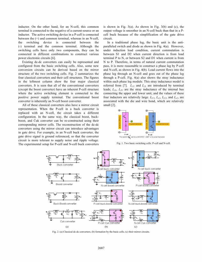
inductor. On the other hand, for an N-cell, this common terminal is connected to the negative of a current-source or an inductor. The active switching device in a P-cell is connected between the (+) and common terminal, whereas in an N-cell, the switching device is connected between the (-) terminal and the common terminal. Although the switching cells have only two components, they can be connected in different combinations to construct various power electronic circuits [6].
Existing dc-dc converters can easily be represented and configured from the basic switching cells. Also, some new conversion circuits can be derived based on the mirror structure of the two switching cells. Fig. 2 summarizes the four classical converters and their cell structures. The figures in the leftmost column show the four major classical converters. It is seen that all of the conventional converters (except the boost converter) have an inherent P-cell structure where the active switching element is connected to the positive power supply terminal. The conventional boost converter is inherently an N-cell boost converter.
All of these classical converters also have a mirror circuit representation. When the P-cell in a buck converter is replaced with an N-cell, the circuit takes a different configuration. In the same way, the classical boost, buck-boost, and Ćuk converter can be re-constructed using their corresponding mirror cells. The reconstruction of the dc-dc converters using the mirror circuit can introduce advantages in gate drive. For example, in an N-cell buck converter, the gate drive signal is ground referenced, so that the converter circuit is more tolerant to supply noise and ripple voltage. The experimental setup for P-cell and N-cell buck converters
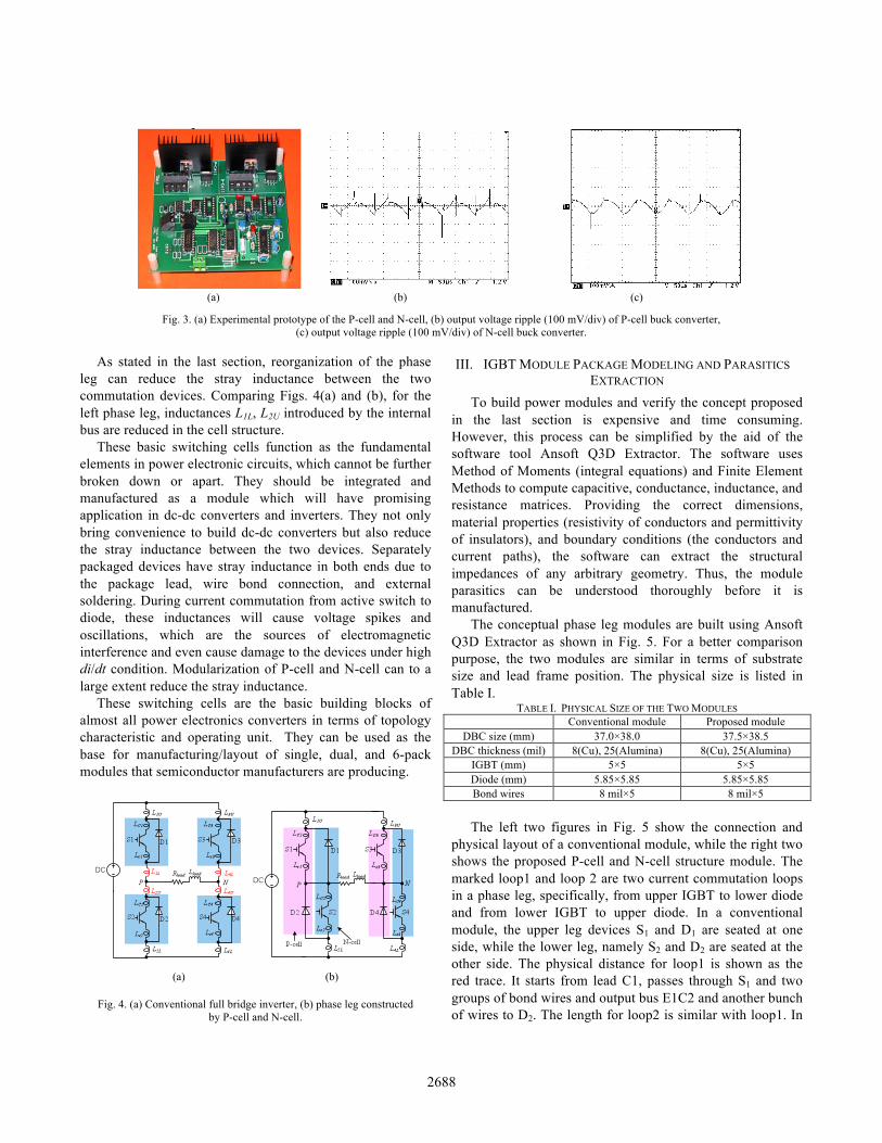
is shown in Fig. 3(a). As shown in Fig. 3(b) and (c), the output voltage is smoother in an N-cell buck than that in a P-cell buck because of the simplification of the gate drive circuit.
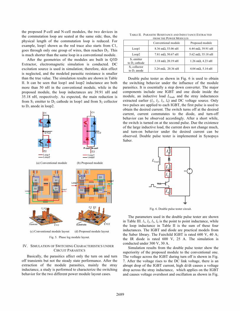
In a traditional phase leg, the basic unit is the anti-paralleled switch and diode as shown in Fig. 4(a). However, under induction load condition, current commutation is between S1 and D2 when current direction is from load terminal P to N, or between S2 and D1 when current is from N to P. Therefore, in terms of natural current commutation pass, it is more reasonable to construct a phase leg by P-cell and N-cell, as shown in Fig. 4(b). Load current flows into the phase leg through an N-cell and goes out of the phase leg through a P-cell. Fig. 4(a) also shows the stray inductance within each phase leg module. This stray inductance model is referred from [7]. L1U and L2L are introduced by terminal leads; L1L, L2U are the stray inductance of the internal bus connecting the upper and lower unit; and the values of these four inductors are relatively large. LC1, Le1, LC2, and Le2, are associated with the die and wire bond, which are relatively small [2].
Fig. 1. Two basic switching cells: P-cell and N-cell.
(a) (b) (c)
Fig. 2. (a) Classical dc-dc converters, (b) formation by the basic cells, (c) their mirror circuits.
2687
(a) (b) (c)
Fig. 3. (a) Experimental prototype of the P-cell and N-cell, (b) output voltage ripple (100 mV/div) of P-cell buck converter, (c) output voltage ripple (100 mV/div) of N-cell buck converter.
As stated in the last section, reorganization of the phase leg can reduce the stray inductance between the two commutation devices. Comparing Figs. 4(a) and (b), for the left phase leg, inductances L1L, L2U introduced by the internal bus are reduced in the cell structure.
These basic switching cells function as the fundamental elements in power electronic circuits, which cannot be further broken down or apart. They should be integrated and manufactured as a module which will have promising application in dc-dc converters and inverters. They not only bring convenience to build dc-dc converters but also reduce the stray inductance between the two devices. Separately packaged devices have stray inductance in both ends due to the package lead, wire bond connection, and external soldering. During current commutation from active switch to diode, these inductances will cause voltage spikes and oscillations, which are the sources of electromagnetic interference and even cause damage to the devices under high di/dt condition. Modularization of P-cell and N-cell can to a large extent reduce the stray inductance.
These switching cells are the basic building blocks of almost all power electronics converters in terms of topology characteristic and operating unit. They can be used as the base for manufacturing/layout of single, dual, and 6-pack modules that semiconductor manufacturers are producing.
(a) (b)
Fig. 4. (a) Conventional full bridge inverter, (b) phase leg constructed by P-cell and N-cell.
III. IGBT MODULE PACKAGE MODELING AND PARASITICS EXTRACTION
To build power modules and verify the concept proposed in the last section is expensive and time consuming. However, this process can be simplified by the aid of the software tool Ansoft Q3D Extractor. The software uses Method of Moments (integral equations) and Finite Element Methods to compute capacitive, conductance, inductance, and resistance matrices. Providing the correct dimensions, material properties (resistivity of conductors and permittivity of insulators), and boundary conditions (the conductors and current paths), the software can extract the structural impedances of any arbitrary geometry. Thus, the module parasitics can be understood thoroughly before it is manufactured.
The conceptual phase leg modules are built using Ansoft Q3D Extractor as shown in Fig. 5. For a better comparison purpose, the two modules are similar in terms of substrate size and lead frame position. The physical size is listed in Table I.
TABLE I. PHYSICAL SIZE OF THE TWO MODULES Conventional module Proposed module
DBC size (mm) 37.0×38.0 37.5×38.5 DBC thickness (mil) 8(Cu), 25(Alumina) 8(Cu), 25(Alumina)
IGBT (mm) 5×5 5×5 Diode (mm) 5.85×5.85 5.85×5.85 Bond wires 8 mil×5 8 mil×5 The left two figures in Fig. 5 show the connection and
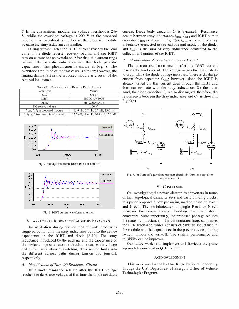
physical layout of a conventional module, while the right two shows the proposed P-cell and N-cell structure module. The marked loop1 and loop 2 are two current commutation loops in a phase leg, specifically, from upper IGBT to lower diode and from lower IGBT to upper diode. In a conventional module, the upper leg devices S1 and D1 are seated at one side, while the lower leg, namely S2 and D2 are seated at the other side. The physical distance for loop1 is shown as the red trace. It starts from lead C1, passes through S1 and two groups of bond wires and output bus E1C2 and another bunch of wires to D2. The length for loop2 is similar with loop1. In
2688
the proposed P-cell and N-cell modules, the two devices in the commutation loop are seated at the same side; thus, the physical length of the commutation loop is reduced. For example, loop1 shown as the red trace also starts from C1, goes through only one group of wires, then reaches D2. This is much shorter than the same loop in a conventional module.
After the geometries of the modules are built in Q3D Extractor, electromagnetic simulation is conducted. DC excitation source is used in simulation; therefore, skin effect is neglected, and the modeled parasitic resistance is smaller than the true value. The simulation results are shown in Table II. It can be seen that loop1 and loop2 inductance are both more than 50 nH in the conventional module, while in the proposed module, the loop inductances are 39.91 nH and 35.18 nH, respectively. As expected, the main reduction is from S1 emitter to D2 cathode in loop1 and from S2 collector to D1 anode in loop2.
(a) Conventional module (b) Proposed module
(c) Conventional module layout (d) Proposed module layout
Fig. 5. Phase leg module layout.
IV. SIMULATION OF SWITCHING CHARACTERISTICS UNDER CIRCUIT PARASITICS
Basically, the parasitics affect only the turn on and turn off transients but not the steady state performance. After the extraction of the module parasitics, mainly the stray inductance, a study is performed to characterize the switching behavior for the two different power module layout cases.
TABLE II. PARASITIC RESISTANCE AND INDUCTANCE EXTRACTED
FROM THE POWER MODULES Conventional module Proposed module
Loop1 8.36 mΩ, 53.06 nH 6.44 mΩ, 39.91 nH
Loop2 7.81 mΩ, 50.67 nH 5.62 mΩ, 35.18 nH S1 emitter
to D2 cathode 3.18 mΩ, 20.19 nH 1.26 mΩ, 4.23 nH
S2 collector to D1 anode 3.24 mΩ, 20.36 nH 4.04 mΩ, 5.14 nH
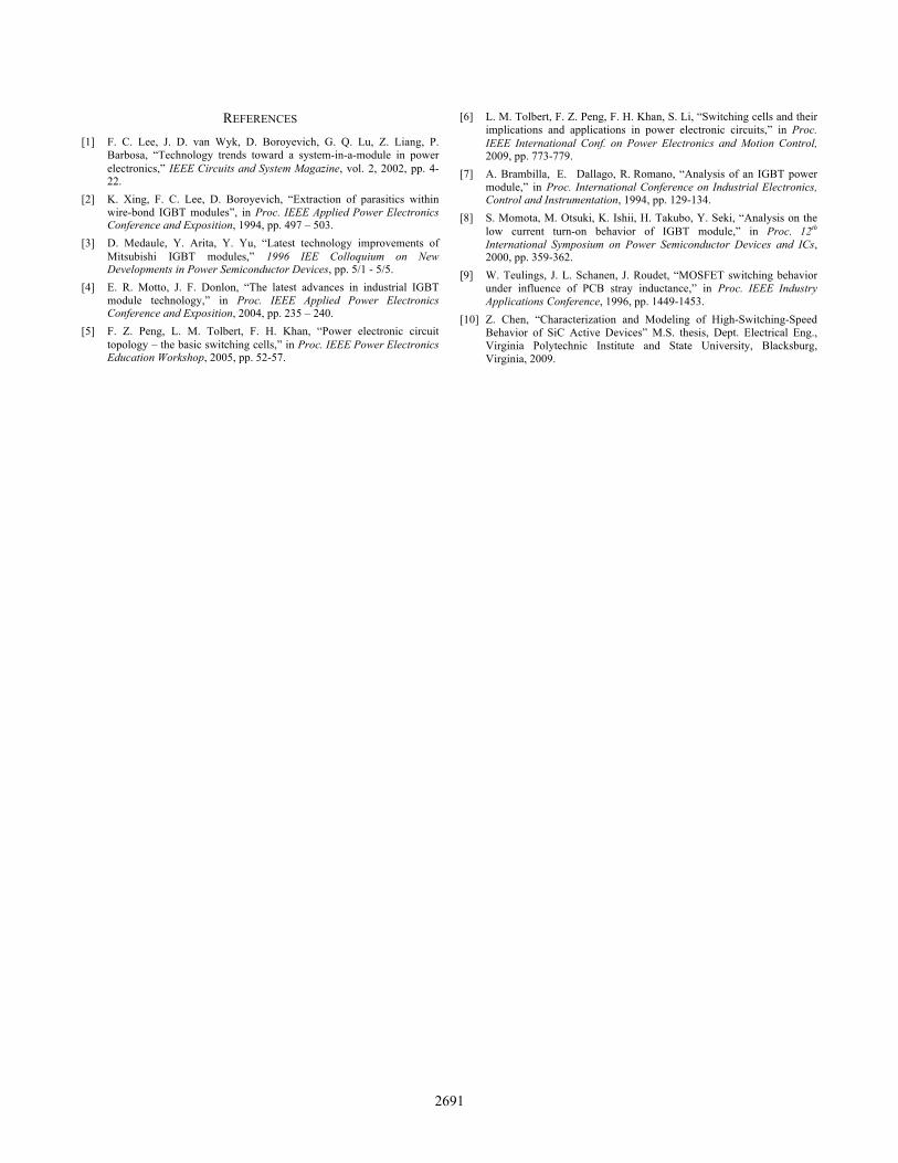
Double pulse tester as shown in Fig. 6 is used to obtain
the switching behavior under the influence of the module parasitics. It is essentially a step down converter. The major components include one IGBT and one diode inside the module, an inductive load Lload, and the stray inductances extracted earlier (l1, l2, l3, l4) and DC voltage source. Only two pulses are applied to each IGBT, the first pulse is used to obtain the desired current. The switch turns off at the desired current, current commutates to the diode, and turn-off behavior can be observed accordingly. After a short while, the switch is turned on at the second pulse. Due the existence of the large inductive load, the current does not change much, and turn-on behavior under the desired current can be observed. Double pulse tester is implemented in Synopsys Saber.
Fig. 6. Double pulse tester circuit.
The parameters used in the double pulse tester are shown in Table III. l1, l2, l3, l4 is the point to point inductance, while the loop inductance in Table II is the sum of these four inductances. The IGBT and diode are practical models from the Saber library. The Fairchild IGBT is rated 600 V, 40 A; the IR diode is rated 600 V, 25 A. The simulation is conducted under 300 V, 30 A.
Simulation results from the double pulse tester show the superiority of the proposed module to the conventional one. The voltage across the IGBT during turn off is shown in Fig. 7. After the voltage rises to the DC link voltage, there is an abrupt drop of the IGBT current, high di/dt causes a voltage drop across the stray inductance, which applies on the IGBT and causes voltage overshoot and oscillation as shown in Fig.
2689
7. In the conventional module, the voltage overshoot is 246 V, while the overshoot voltage is 200 V in the proposed module. The overshoot is smaller in the proposed module because the stray inductance is smaller.
During turn-on, after the IGBT current reaches the load current, the diode reverse recovery begins, and the IGBT turn-on current has an overshoot. After that, this current rings between the parasitic inductance and the diode parasitic capacitance. This phenomenon is shown in Fig. 8. The overshoot amplitude of the two cases is similar; however, the ringing damps fast in the proposed module as a result of the reduced inductance.
TABLE III. PARAMETERS IN DOUBLE PULSE TESTER Parameters Values
Lload 500 µH IGBT HGTG40N60B3 Diode HFA25D60ACE
DC source voltage 300 V l1, l2, l3, l4 in proposed module 15.0 nH, 2.7 nH, 2.7 nH, 15.0 nH
l1, l2, l3, l4 in conventional module 15.3 nH, 10.4 nH, 10.4 nH, 15.3 nH
Fig. 7. Voltage waveform across IGBT at turn-off.
Fig. 8. IGBT current waveform at turn-on.
V. ANALYSIS OF RESONANCE CAUSED BY PARASITICS The oscillation during turn-on and turn-off process is
triggered by not only the stray inductance but also the device capacitance in the IGBT and diode [8-10]. The stray inductance introduced by the package and the capacitance of the device compose a resonant circuit that causes the voltage and current oscillation at switching. This section looks into the different current paths during turn-on and turn-off, respectively.
A. Identification of Turn-Off Resonance Circuit The turn-off resonance sets up after the IGBT voltage
reaches the dc source voltage; at this time the diode conducts
current. Diode body capacitor CJ is bypassed. Resonance occurs between stray inductances ldiode, lIGBT and IGBT output capacitor COES as shown in Fig. 9(a). ldiode is the sum of stray inductance connected to the cathode and anode of the diode, and lIGBT is the sum of stray inductance connected to the collector and emitter of the IGBT.
B. Identification of Turn-On Resonance Circuit The turn-on oscillation occurs after the IGBT current
reaches the load current. The voltage across the IGBT starts to drop, while the diode voltage increases. There is discharge current from capacitor COES; however, since the IGBT is already turned on, this current goes through the IGBT and does not resonate with the stray inductance. On the other hand, the diode capacitor CJ is also discharged; therefore, the resonance is between the stray inductance and CJ, as shown in Fig. 9(b).
(a) (b)
Fig. 9. (a) Turn-off equivalent resonant circuit, (b) Turn-on equivalent resonant circuit.
VI. CONCLUSION On investigating the power electronics converters in terms
of their topological characteristics and basic building blocks, this paper proposes a new packaging method based on P-cell and N-cell. The modularization of single P-cell or N-cell increases the convenience of building dc-dc and dc-ac converters. More importantly, the proposed package reduces the parasitic inductance in the commutation loop, suppresses the LCR resonance, which consists of parasitic inductance in the module and the capacitance in the power devices, during switch turn-on and turn-off. The system performance and reliability can be improved.
Our future work is to implement and fabricate the phase leg modules modeled in Q3D Extractor.
ACKNOWLEDGMENT
This work was funded by Oak Ridge National Laboratory through the U.S. Department of Energy’s Office of Vehicle Technologies Program.
Conventional
Proposed
2690
REFERENCES [1] F. C. Lee, J. D. van Wyk, D. Boroyevich, G. Q. Lu, Z. Liang, P.
Barbosa, “Technology trends toward a system-in-a-module in power electronics,” IEEE Circuits and System Magazine, vol. 2, 2002, pp. 4-22.
[2] K. Xing, F. C. Lee, D. Boroyevich, “Extraction of parasitics within wire-bond IGBT modules”, in Proc. IEEE Applied Power Electronics Conference and Exposition, 1994, pp. 497 – 503.
[3] D. Medaule, Y. Arita, Y. Yu, “Latest technology improvements of Mitsubishi IGBT modules,” 1996 IEE Colloquium on New Developments in Power Semiconductor Devices, pp. 5/1 - 5/5.
[4] E. R. Motto, J. F. Donlon, “The latest advances in industrial IGBT module technology,” in Proc. IEEE Applied Power Electronics Conference and Exposition, 2004, pp. 235 – 240.
[5] F. Z. Peng, L. M. Tolbert, F. H. Khan, “Power electronic circuit topology – the basic switching cells,” in Proc. IEEE Power Electronics Education Workshop, 2005, pp. 52-57.
[6] L. M. Tolbert, F. Z. Peng, F. H. Khan, S. Li, “Switching cells and their implications and applications in power electronic circuits,” in Proc. IEEE International Conf. on Power Electronics and Motion Control, 2009, pp. 773-779.
[7] A. Brambilla, E. Dallago, R. Romano, “Analysis of an IGBT power module,” in Proc. International Conference on Industrial Electronics, Control and Instrumentation, 1994, pp. 129-134.
[8] S. Momota, M. Otsuki, K. Ishii, H. Takubo, Y. Seki, “Analysis on the low current turn-on behavior of IGBT module,” in Proc. 12th International Symposium on Power Semiconductor Devices and ICs, 2000, pp. 359-362.
[9] W. Teulings, J. L. Schanen, J. Roudet, “MOSFET switching behavior under influence of PCB stray inductance,” in Proc. IEEE Industry Applications Conference, 1996, pp. 1449-1453.
[10] Z. Chen, “Characterization and Modeling of High-Switching-Speed Behavior of SiC Active Devices” M.S. thesis, Dept. Electrical Eng., Virginia Polytechnic Institute and State University, Blacksburg, Virginia, 2009.
2691