Embed Size (px)
Citation preview
© 2018 Microsemi, a wholly owned subsidiary of Microchip Technology Inc. 1
SiC Diode and MOSFET product portfolioLow stray inductance power modulePascal Ducluzeau – BDM power modulesDiscrete & Integrated Solutions Group
Fortronic, ModenaJune 28th, 2018
2© 2018 Microsemi
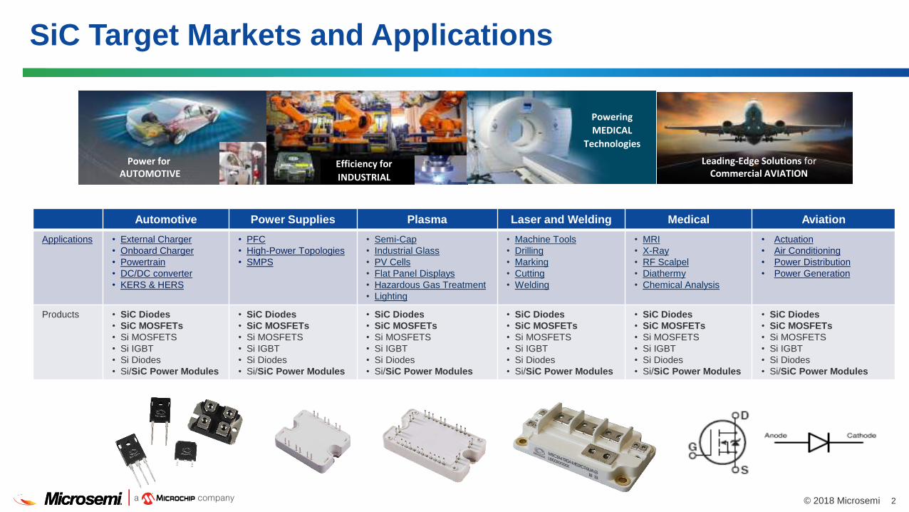
SiC Target Markets and Applications
Automotive Power Supplies Plasma Laser and Welding Medical Aviation
Applications • External Charger• Onboard Charger• Powertrain• DC/DC converter• KERS & HERS
• PFC• High-Power Topologies• SMPS
• Semi-Cap• Industrial Glass• PV Cells• Flat Panel Displays• Hazardous Gas Treatment• Lighting
• Machine Tools• Drilling• Marking• Cutting• Welding
• MRI• X-Ray • RF Scalpel• Diathermy• Chemical Analysis
• Actuation • Air Conditioning• Power Distribution• Power Generation
Products • SiC Diodes• SiC MOSFETs• Si MOSFETS• Si IGBT• Si Diodes • Si/SiC Power Modules
• SiC Diodes • SiC MOSFETs • Si MOSFETS• Si IGBT• Si Diodes• Si/SiC Power Modules
• SiC Diodes• SiC MOSFETs• Si MOSFETS• Si IGBT• Si Diodes• Si/SiC Power Modules
• SiC Diodes • SiC MOSFETs • Si MOSFETS• Si IGBT• Si Diodes• Si/SiC Power Modules
• SiC Diodes• SiC MOSFETs • Si MOSFETS• Si IGBT• Si Diodes• Si/SiC Power Modules
• SiC Diodes• SiC MOSFETs• Si MOSFETS• Si IGBT• Si Diodes• Si/SiC Power Modules
Power for AUTOMOTIVE
Efficiency for
INDUSTRIAL
Leading-Edge Solutions for Commercial AVIATION
Powering
MEDICAL
Technologies
SiC Discrete MOSFET
4© 2018 Microsemi
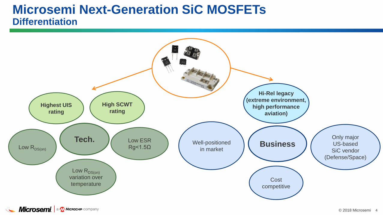
Microsemi Next-Generation SiC MOSFETsDifferentiation
Tech.
Highest UIS rating
Only major US-based SiC vendor
(Defense/Space)
Well-positioned in market
High SCWT rating
Low RDS(on)variation over temperature
BusinessLow RDS(on)
Cost competitive
Low ESRRg<1.5Ω
Hi-Rel legacy (extreme environment,
high performance aviation)
5© 2018 Microsemi
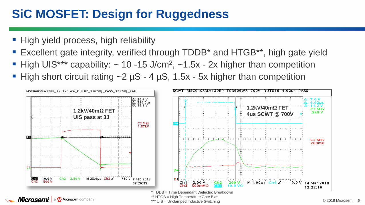
High yield process, high reliability Excellent gate integrity, verified through TDDB* and HTGB**, high gate yield High UIS*** capability: ~ 10 -15 J/cm2, ~1.5x - 2x higher than competition High short circuit rating ~2 µS - 4 µS, 1.5x - 5x higher than competition
1.2kV/40mΩ FETUIS pass at 3J
1.2kV/40mΩ FET4us SCWT @ 700V
* TDDB = Time Dependant Dielectric Breakdown** HTGB = High Temperature Gate Bias*** UIS = Unclamped Inductive Switching
SiC MOSFET: Design for Ruggedness
6© 2018 Microsemi
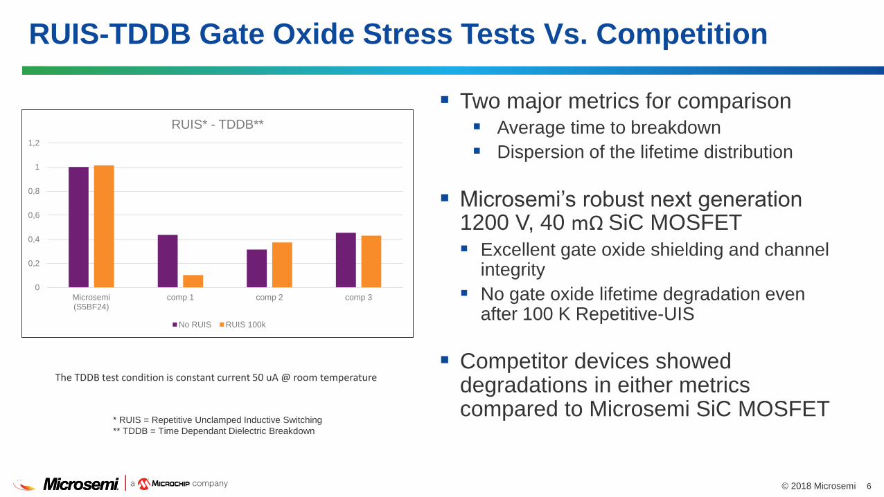
RUIS-TDDB Gate Oxide Stress Tests Vs. Competition
Two major metrics for comparison Average time to breakdown Dispersion of the lifetime distribution
Microsemi’s robust next generation 1200 V, 40 mΩ SiC MOSFET Excellent gate oxide shielding and channel
integrity No gate oxide lifetime degradation even
after 100 K Repetitive-UIS
Competitor devices showed degradations in either metrics compared to Microsemi SiC MOSFET
0
0,2
0,4
0,6
0,8
1
1,2
Microsemi(S5BF24)
comp 1 comp 2 comp 3
RUIS* - TDDB**
No RUIS RUIS 100k
The TDDB test condition is constant current 50 uA @ room temperature
* RUIS = Repetitive Unclamped Inductive Switching** TDDB = Time Dependant Dielectric Breakdown
7© 2018 Microsemi
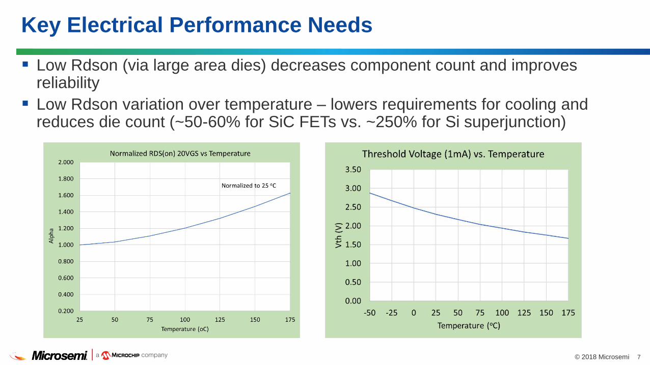
Low Rdson (via large area dies) decreases component count and improves reliability
Low Rdson variation over temperature – lowers requirements for cooling and reduces die count (~50-60% for SiC FETs vs. ~250% for Si superjunction)
Key Electrical Performance Needs
8© 2018 Microsemi
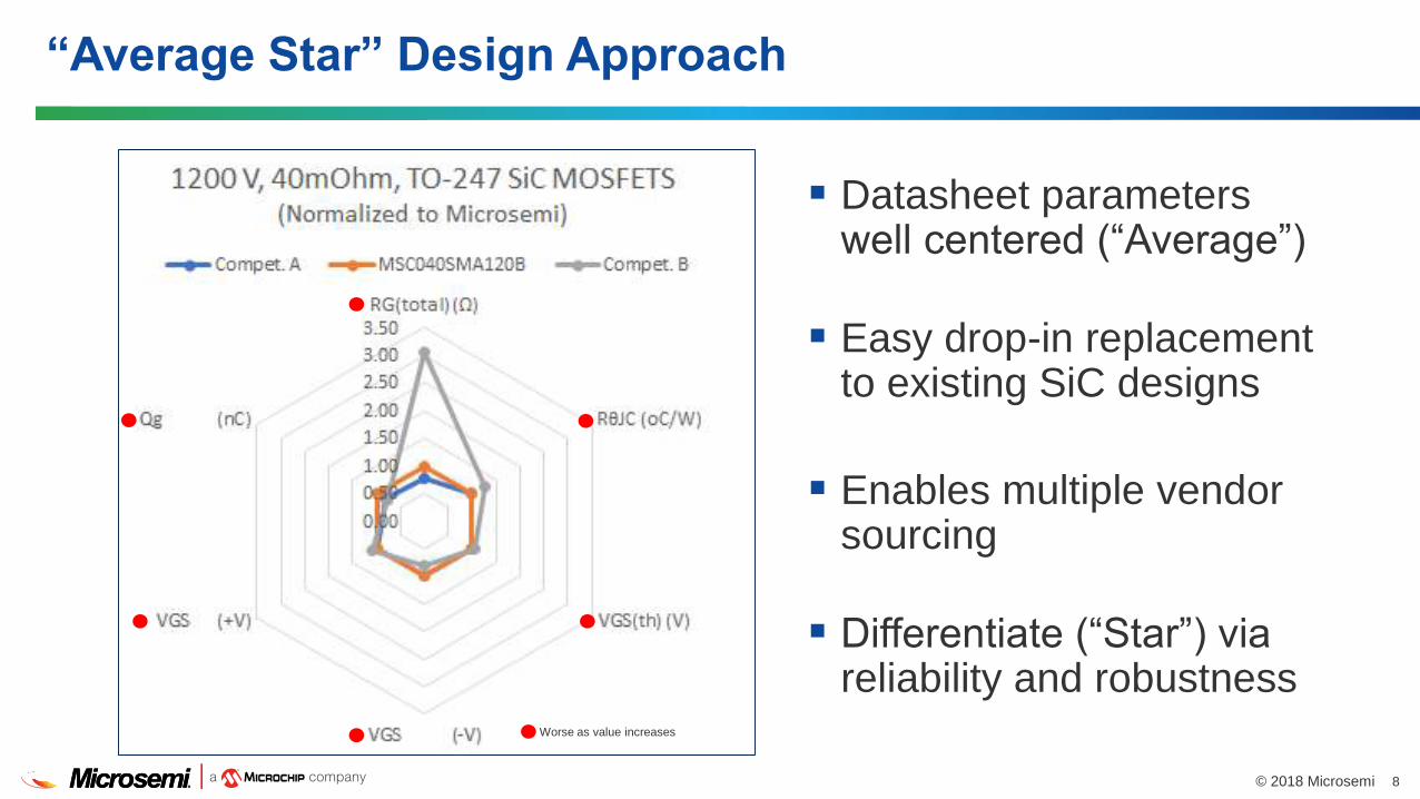
Worse as value increases
Datasheet parameters well centered (“Average”)
Easy drop-in replacement to existing SiC designs
Enables multiple vendor sourcing
Differentiate (“Star”) via reliability and robustness
“Average Star” Design Approach
9© 2018 Microsemi
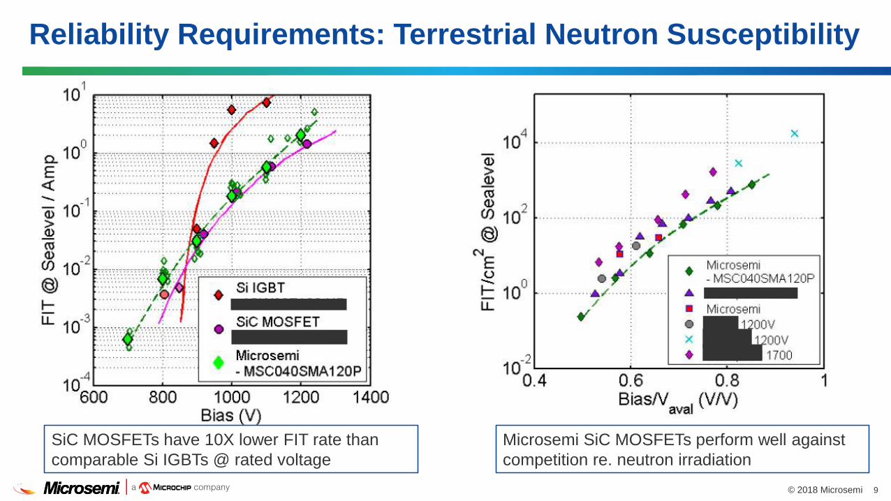
Reliability Requirements: Terrestrial Neutron Susceptibility
SiC MOSFETs have 10X lower FIT rate than comparable Si IGBTs @ rated voltage
Microsemi SiC MOSFETs perform well against competition re. neutron irradiation
10© 2018 Microsemi
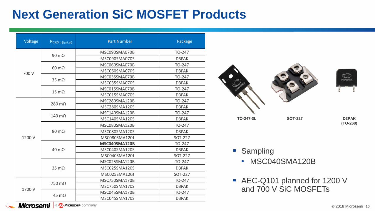
Next Generation SiC MOSFET Products
Sampling • MSC040SMA120B
AEC-Q101 planned for 1200 V and 700 V SiC MOSFETs
Voltage RDS(On) (typical) Part Number Package
700 V
90 mΩMSC090SMA070B TO-247
MSC090SMA070S D3PAK
60 mΩMSC060SMA070B TO-247
MSC060SMA070S D3PAK
35 mΩMSC035SMA070B TO-247
MSC035SMA070S D3PAK
15 mΩMSC015SMA070B TO-247
MSC015SMA070S D3PAK
1200 V
280 mΩMSC280SMA120B TO-247
MSC280SMA120S D3PAK
140 mΩMSC140SMA120B TO-247
MSC140SMA120S D3PAK
80 mΩ
MSC080SMA120B TO-247
MSC080SMA120S D3PAK
MSC080SMA120J SOT-227
40 mΩ
MSC040SMA120B TO-247
MSC040SMA120S D3PAK
MSC040SMA120J SOT-227
25 mΩ
MSC025SMA120B TO-247
MSC025SMA120S D3PAK
MSC025SMA120J SOT-227
1700 V
750 mΩMSC750SMA170B TO-247
MSC750SMA170S D3PAK
45 mΩMSC045SMA170B TO-247
MSC045SMA170S D3PAK
TO-247-3L SOT-227 D3PAK(TO-268)
11© 2018 Microsemi
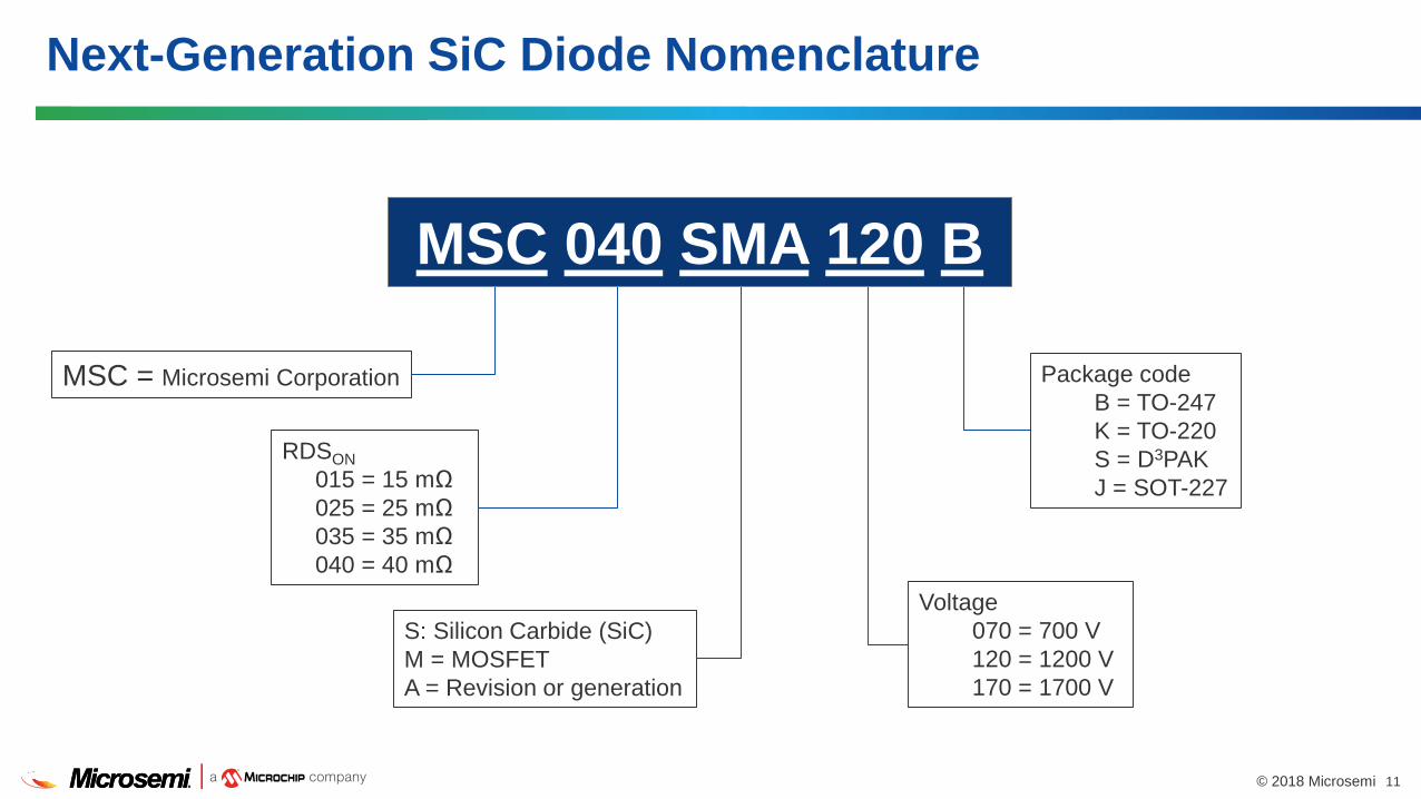
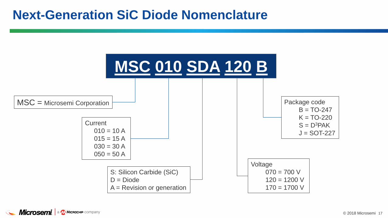
Next-Generation SiC Diode Nomenclature
MSC = Microsemi Corporation
RDSON015 = 15 mΩ
025 = 25 mΩ
035 = 35 mΩ
040 = 40 mΩ
S: Silicon Carbide (SiC)M = MOSFET A = Revision or generation
Voltage 070 = 700 V120 = 1200 V170 = 1700 V
Package codeB = TO-247K = TO-220S = D3PAKJ = SOT-227
MSC 040 SMA 120 B

SiC Discrete diode
13© 2018 Microsemi
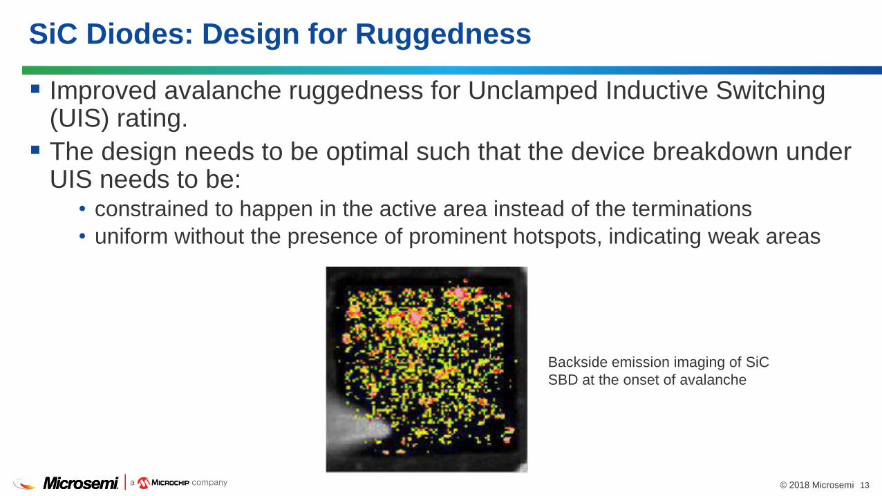
Improved avalanche ruggedness for Unclamped Inductive Switching (UIS) rating.
The design needs to be optimal such that the device breakdown under UIS needs to be:
• constrained to happen in the active area instead of the terminations• uniform without the presence of prominent hotspots, indicating weak areas
SiC Diodes: Design for Ruggedness
Backside emission imaging of SiCSBD at the onset of avalanche
14© 2018 Microsemi
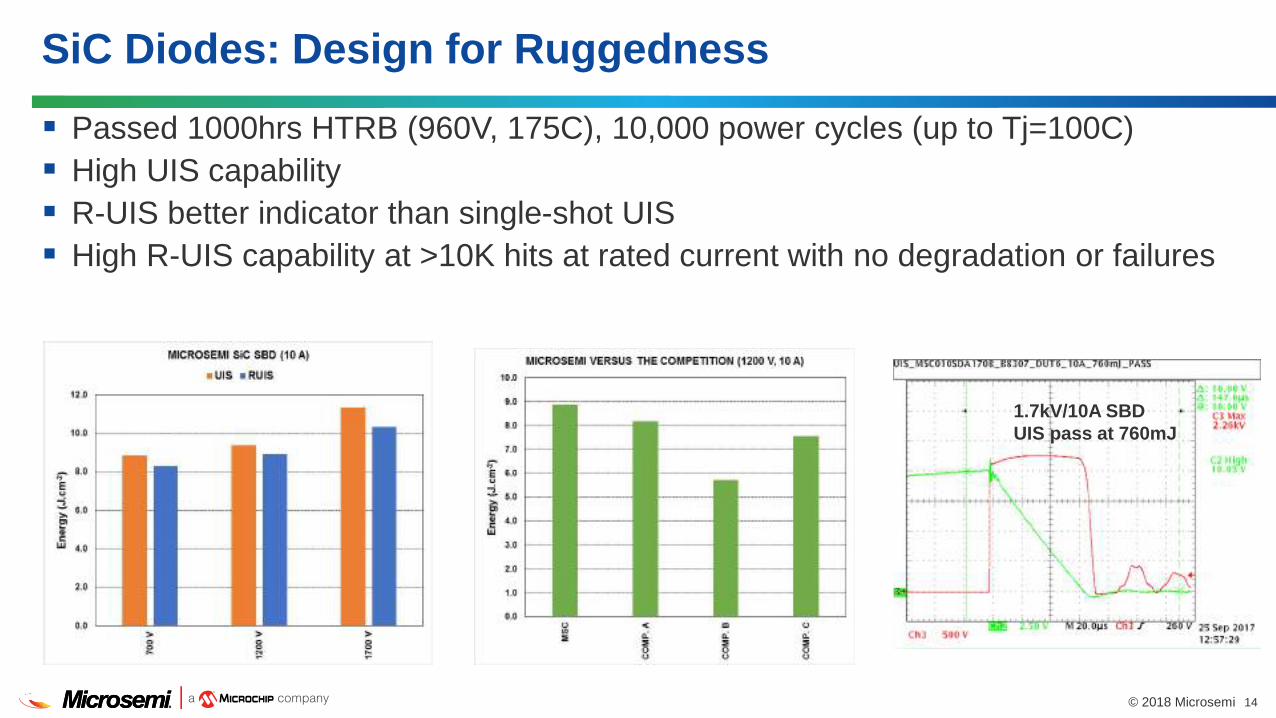
Passed 1000hrs HTRB (960V, 175C), 10,000 power cycles (up to Tj=100C) High UIS capability R-UIS better indicator than single-shot UIS High R-UIS capability at >10K hits at rated current with no degradation or failures
SiC Diodes: Design for Ruggedness
1.7kV/10A SBDUIS pass at 760mJ
15© 2018 Microsemi
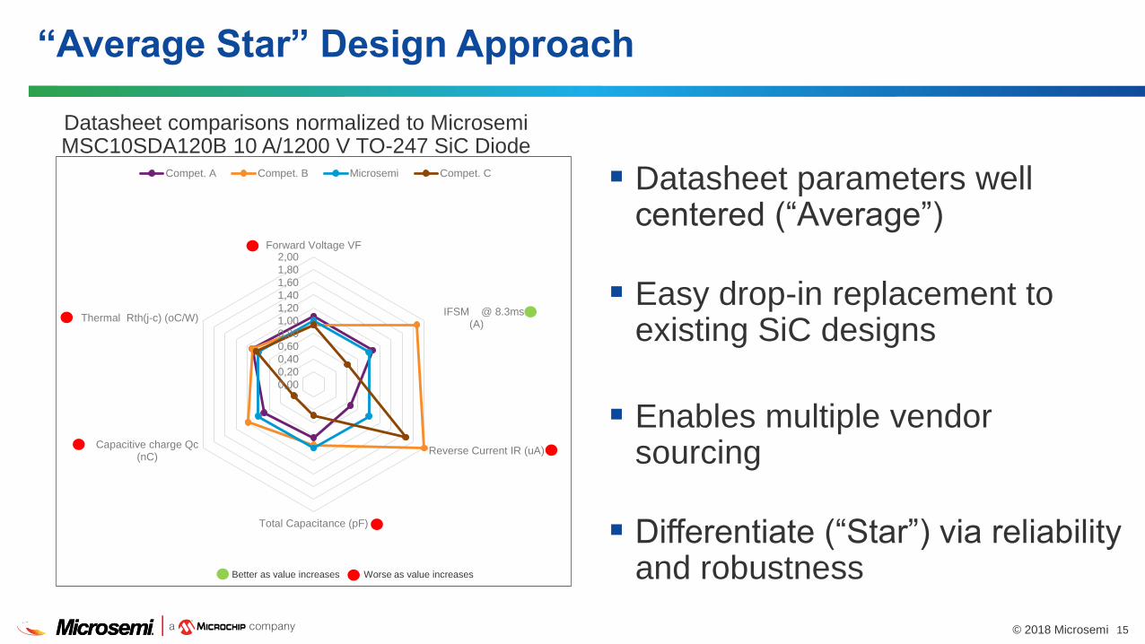
“Average Star” Design Approach
Datasheet comparisons normalized to MicrosemiMSC10SDA120B 10 A/1200 V TO-247 SiC Diode
Datasheet parameters well centered (“Average”)
Easy drop-in replacement to existing SiC designs
Enables multiple vendor sourcing
Differentiate (“Star”) via reliability and robustness
0,000,200,400,600,801,001,201,401,601,802,00
Forward Voltage VF
IFSM @ 8.3ms(A)
Reverse Current IR (uA)
Total Capacitance (pF)
Capacitive charge Qc(nC)
Thermal Rth(j-c) (oC/W)
Compet. A Compet. B Microsemi Compet. C
Better as value increases Worse as value increases
16© 2018 Microsemi
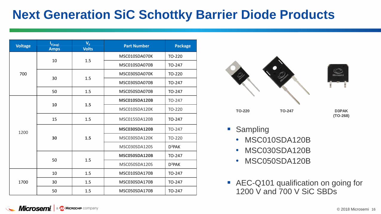
Next Generation SiC Schottky Barrier Diode Products
Sampling • MSC010SDA120B• MSC030SDA120B• MSC050SDA120B
AEC-Q101 qualification on going for 1200 V and 700 V SiC SBDs
VoltageIF(avg) VF Part Number Package Amps Volts
700
10 1.5MSC010SDA070K TO-220
MSC010SDA070B TO-247
30 1.5MSC030SDA070K TO-220
MSC030SDA070B TO-247
50 1.5 MSC050SDA070B TO-247
1200
10 1.5MSC010SDA120B TO-247
MSC010SDA120K TO-220
15 1.5 MSC015SDA120B TO-247
30 1.5
MSC030SDA120B TO-247
MSC030SDA120K TO-220
MSC030SDA120S D3PAK
50 1.5MSC050SDA120B TO-247
MSC050SDA120S D3PAK
1700
10 1.5 MSC010SDA170B TO-247
30 1.5 MSC030SDA170B TO-247
50 1.5 MSC050SDA170B TO-247
TO-247 D3PAK (TO-268)
TO-220
17© 2018 Microsemi
Next-Generation SiC Diode Nomenclature
MSC = Microsemi Corporation
Current010 = 10 A015 = 15 A030 = 30 A050 = 50 A
S: Silicon Carbide (SiC)D = Diode A = Revision or generation
Voltage 070 = 700 V120 = 1200 V170 = 1700 V
Package codeB = TO-247K = TO-220S = D3PAKJ = SOT-227
MSC 010 SDA 120 B

SiC Power Modules
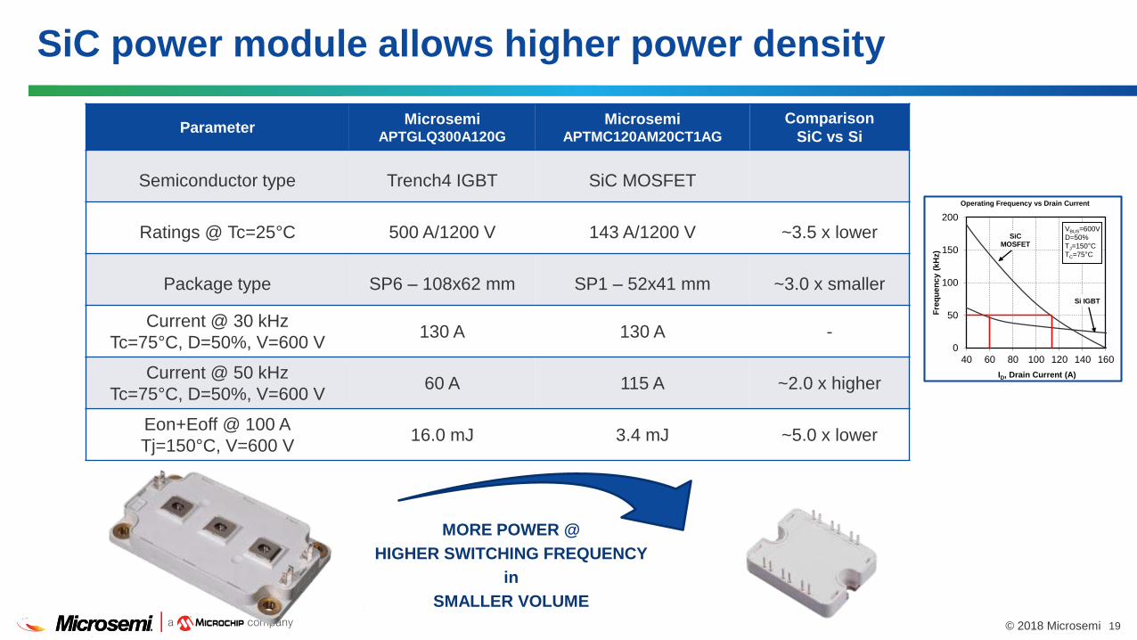
19© 2018 Microsemi
MORE POWER @HIGHER SWITCHING FREQUENCY
in SMALLER VOLUME
Parameter MicrosemiAPTGLQ300A120G
MicrosemiAPTMC120AM20CT1AG
ComparisonSiC vs Si
Semiconductor type Trench4 IGBT SiC MOSFET
Ratings @ Tc=25°C 500 A/1200 V 143 A/1200 V ~3.5 x lower
Package type SP6 – 108x62 mm SP1 – 52x41 mm ~3.0 x smaller
Current @ 30 kHzTc=75°C, D=50%, V=600 V
130 A 130 A -
Current @ 50 kHzTc=75°C, D=50%, V=600 V
60 A 115 A ~2.0 x higher
Eon+Eoff @ 100 ATj=150°C, V=600 V
16.0 mJ 3.4 mJ ~5.0 x lower
SiCMOSFET
Si IGBT
0
50
100
150
200
40 60 80 100 120 140 160
Fre
qu
ency
(kH
z)
ID, Drain Current (A)
Operating Frequency vs Drain Current
VBUS=600VD=50%TJ=150°CTC=75°C
SiC power module allows higher power density
20© 2018 Microsemi
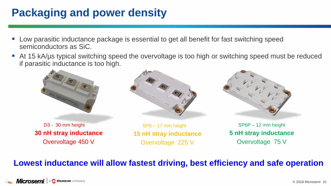
Packaging and power density
Low parasitic inductance package is essential to get all benefit for fast switching speed semiconductors as SiC.
At 15 kA/µs typical switching speed the overvoltage is too high or switching speed must be reduced if parasitic inductance is too high.
Lowest inductance will allow fastest driving, best efficiency and safe operation
D3 - 30 mm height
30 nH stray inductanceOvervoltage 450 V
SP6 – 17 mm height
15 nH stray inductance Overvoltage 225 V
SP6P – 12 mm height
5 nH stray inductanceOvervoltage 75 V
21© 2018 Microsemi
Develop a standard package targetting <5 nH stray inductance to beused in high switching frequency applications with SiC semi-conductors.
Offer a standard footprint package recognized on the market.
Benefit from one layout to use different die vendors to compare easilydifferent performances and make the right choice for the application.
Very low inductance package: Objectives
22© 2018 Microsemi
Optimized layout for multi SiC MOSFET and Diode chips assembly in phase leg topology.
Symmetrical design to accept up to 12 SiC MOSFET chips in parallelper switch to offer a total RDSON down to 2 mΩ per switch.
All die in parallel with its own gate series resistor for homogenouscurrent balancing.
High current capability up to 600A at very fast switching frequency. Optional mix of assembly materials to better address various markets
and applications:oAlN or Si3N4 substratesoCopper or AlSiC baseplatesoPin fins base plate option for dircet liquid cooling
Very low inductance package: Realization
23© 2018 Microsemi
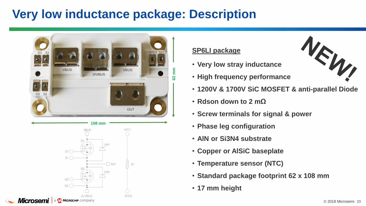
Very low inductance package: Description
VBUS VBUS0/VBUS
OUT
G1 S1
G2 S2
NTC2 NTC1
• Very low stray inductance
• High frequency performance
• 1200V & 1700V SiC MOSFET & anti-parallel Diode
• Rdson down to 2 mΩ
• Screw terminals for signal & power
• Phase leg configuration
• AlN or Si3N4 substrate
• Copper or AlSiC baseplate
• Temperature sensor (NTC)
• Standard package footprint 62 x 108 mm
• 17 mm height
62 m
m
108 mm
SP6LI package
24© 2018 Microsemi
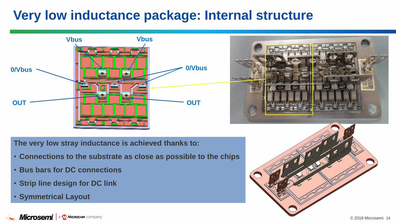
Very low inductance package: Internal structure
The very low stray inductance is achieved thanks to:
• Connections to the substrate as close as possible to the chips
• Bus bars for DC connections
• Strip line design for DC link
• Symmetrical Layout
VbusVbus
0/Vbus 0/Vbus
OUTOUT
25© 2018 Microsemi
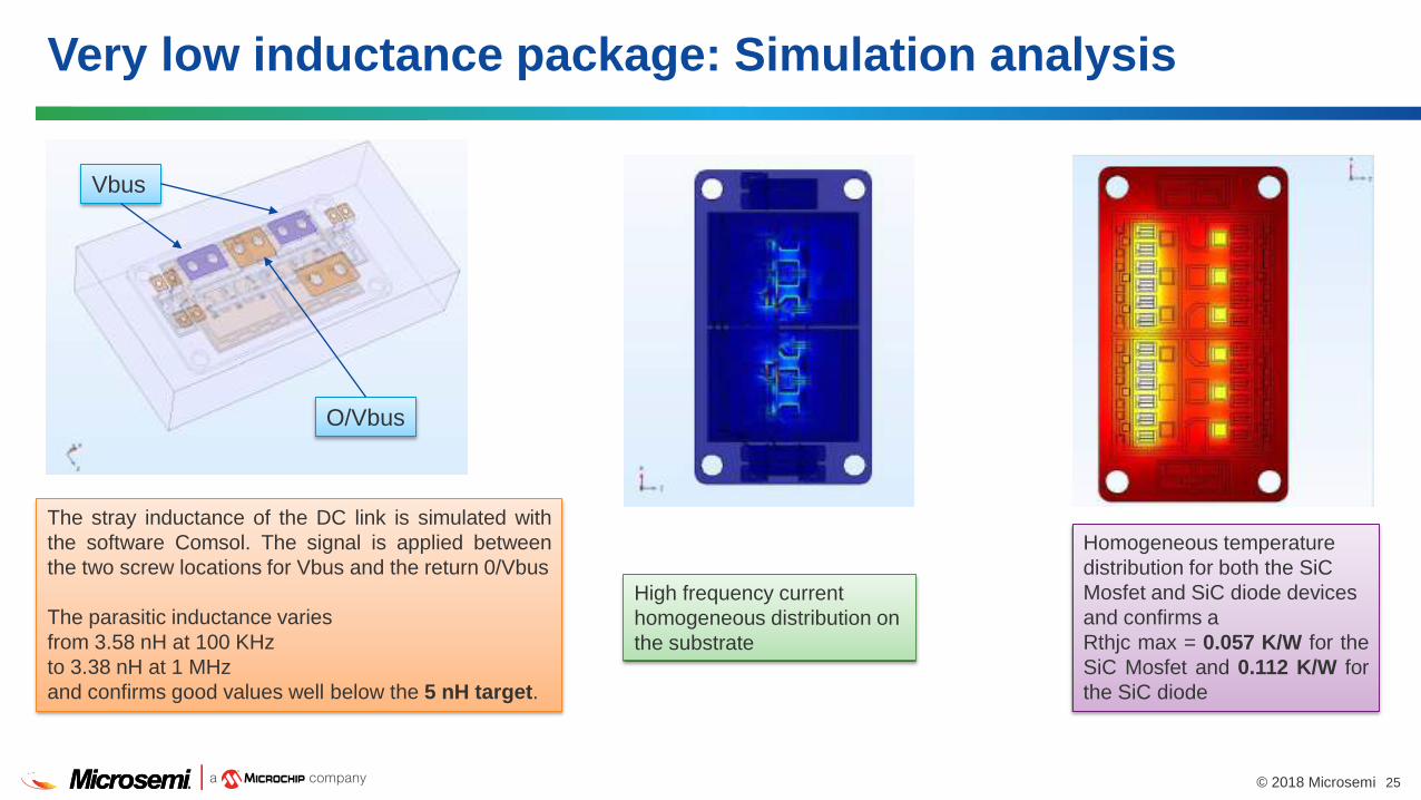
High frequency current homogeneous distribution on the substrate
Homogeneous temperature distribution for both the SiCMosfet and SiC diode devices and confirms a Rthjc max = 0.057 K/W for theSiC Mosfet and 0.112 K/W forthe SiC diode
Very low inductance package: Simulation analysis
Vbus
O/Vbus
The stray inductance of the DC link is simulated withthe software Comsol. The signal is applied betweenthe two screw locations for Vbus and the return 0/Vbus
The parasitic inductance variesfrom 3.58 nH at 100 KHzto 3.38 nH at 1 MHzand confirms good values well below the 5 nH target.
26© 2018 Microsemi
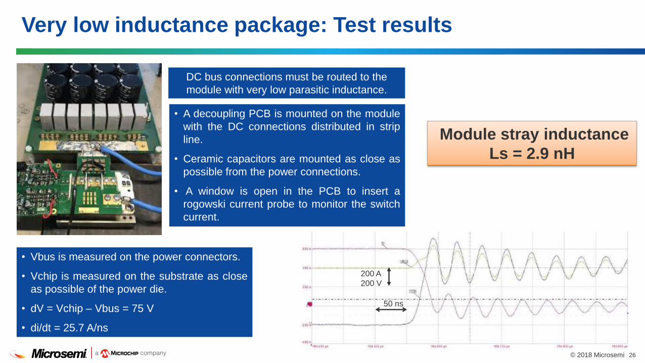
Very low inductance package: Test results
200 A200 V
50 ns
• Vbus is measured on the power connectors.
• Vchip is measured on the substrate as closeas possible of the power die.
• dV = Vchip – Vbus = 75 V
• di/dt = 25.7 A/ns
Module stray inductance Ls = 2.9 nH
• A decoupling PCB is mounted on the modulewith the DC connections distributed in stripline.
• Ceramic capacitors are mounted as close aspossible from the power connections.
• A window is open in the PCB to insert arogowski current probe to monitor the switchcurrent.
DC bus connections must be routed to the module with very low parasitic inductance.
27© 2018 Microsemi
Hard switching
0
50
100
150
200
250
300
350
400
50 200 350 500 650 800
Fre
qu
enc
y (k
Hz)
ID, Drain Current (A)
Operating Frequency vs Drain Current
VBUS=600VD=50%RG=0.25Ω
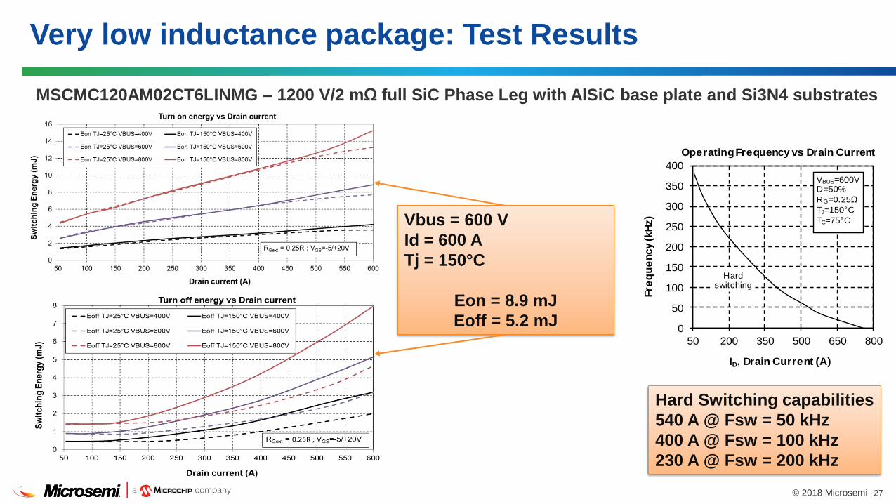
TJ=150°CTC=75°CVbus = 600 V
Id = 600 A Tj = 150°C
Eon = 8.9 mJEoff = 5.2 mJ
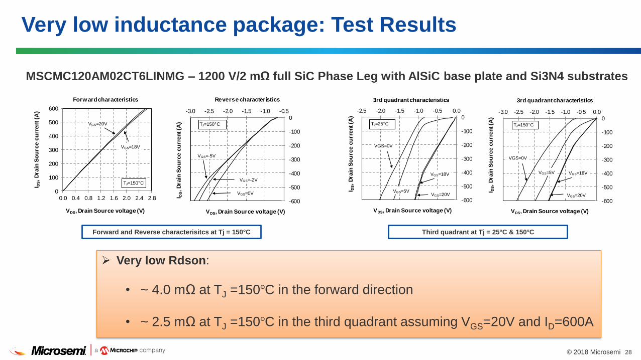
MSCMC120AM02CT6LINMG – 1200 V/2 mΩ full SiC Phase Leg with AlSiC base plate and Si3N4 substrates
Very low inductance package: Test Results
Hard Switching capabilities540 A @ Fsw = 50 kHz400 A @ Fsw = 100 kHz230 A @ Fsw = 200 kHz
28© 2018 Microsemi
VGS=18V
VGS=20V
0
100
200
300
400
500
600
0.0 0.4 0.8 1.2 1.6 2.0 2.4 2.8
I DS, D
rain
So
urc
e c
urr
ent (
A)
VDS, Drain Source voltage (V)
Forward characteristics
TJ=150°CVGS=-2V
VGS=0V
VGS=-5V
-600
-500
-400
-300
-200
-100
0-3.0 -2.5 -2.0 -1.5 -1.0 -0.5
I DS, D
rain
So
urc
e c
urr
ent (
A)
VDS, Drain Source voltage (V)
Reverse characteristics
TJ=150°C
VGS=18V
VGS=0V
VGS=5VVGS=20V
-600
-500
-400
-300
-200
-100
0-2.5 -2.0 -1.5 -1.0 -0.5 0.0
I DS, D
rain
So
urc
e c
urr
ent (
A)
VDS, Drain Source voltage (V)
3rd quadrant characteristics
TJ=25°C
VGS=18V
VGS=0V
VGS=5V
VGS=20V-600
-500
-400
-300
-200
-100
0-3.0 -2.5 -2.0 -1.5 -1.0 -0.5 0.0
I DS, D
rain
So
urc
e c
urr
ent (
A)
VDS, Drain Source voltage (V)
3rd quadrant characteristics
TJ=150°C
Forward and Reverse characterisitcs at Tj = 150°C
Very low Rdson:
• ~ 4.0 mΩ at TJ =150°C in the forward direction
• ~ 2.5 mΩ at TJ =150°C in the third quadrant assuming VGS=20V and ID=600A
Very low inductance package: Test Results
Third quadrant at Tj = 25°C & 150°C
MSCMC120AM02CT6LINMG – 1200 V/2 mΩ full SiC Phase Leg with AlSiC base plate and Si3N4 substrates
29© 2018 Microsemi
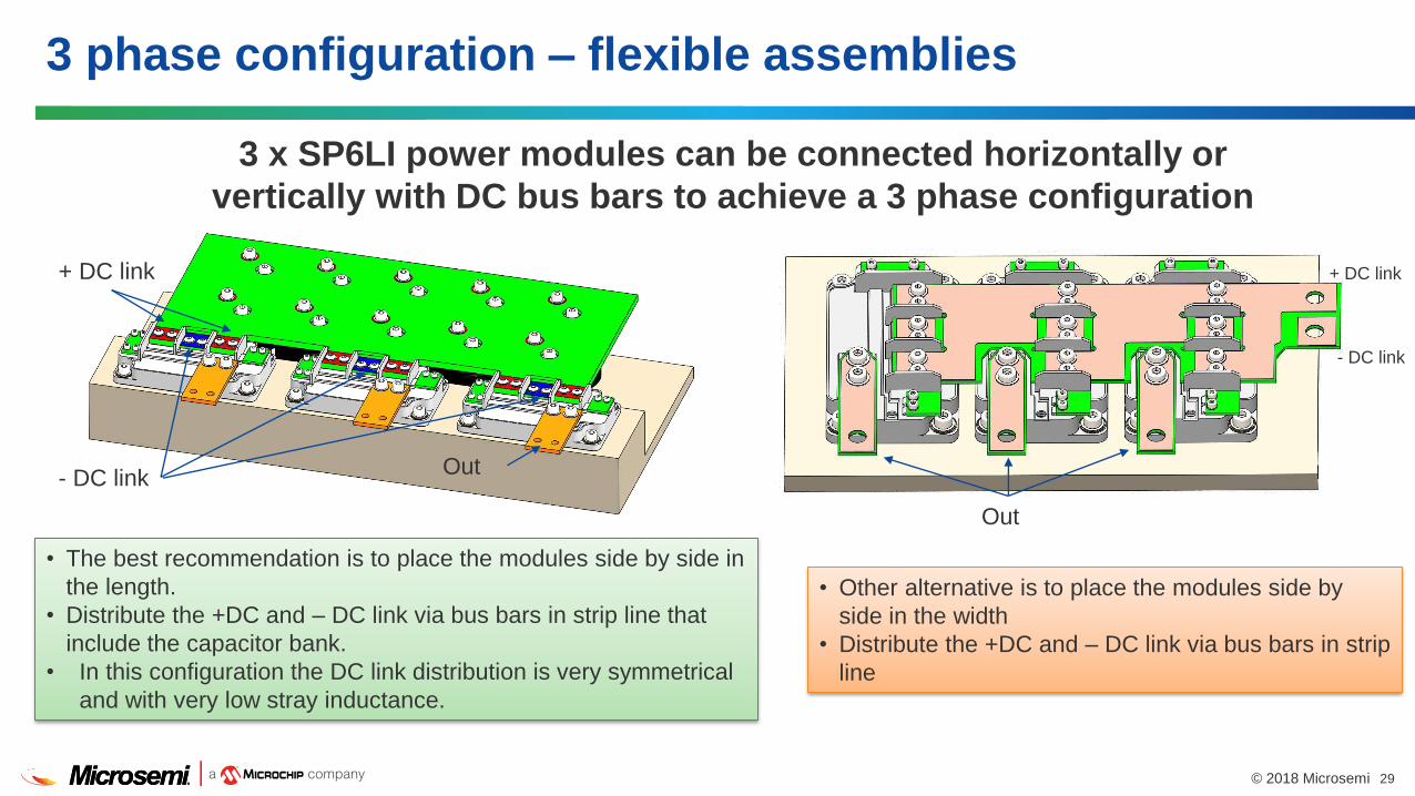
3 phase configuration – flexible assemblies
3 x SP6LI power modules can be connected horizontally or vertically with DC bus bars to achieve a 3 phase configuration
• Other alternative is to place the modules side by side in the width
• Distribute the +DC and – DC link via bus bars in stripline
• The best recommendation is to place the modules side by side in the length.
• Distribute the +DC and – DC link via bus bars in strip line thatinclude the capacitor bank.
• In this configuration the DC link distribution is very symmetricaland with very low stray inductance.
+ DC link
- DC link Out
+ DC link
- DC link
Out
30© 2018 Microsemi
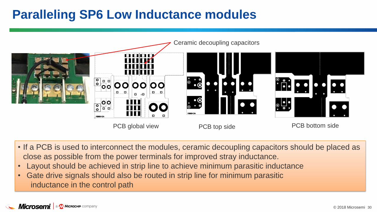
Paralleling SP6 Low Inductance modules
• If a PCB is used to interconnect the modules, ceramic decoupling capacitors should be placed as close as possible from the power terminals for improved stray inductance.
• Layout should be achieved in strip line to achieve minimum parasitic inductance• Gate drive signals should also be routed in strip line for minimum parasitic
inductance in the control path
PCB global view PCB top side PCB bottom side
Ceramic decoupling capacitors
31© 2018 Microsemi
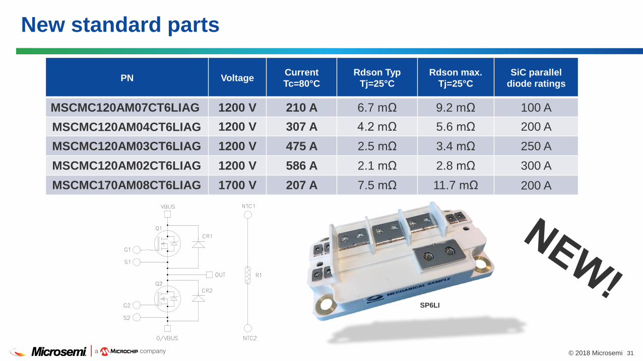
New standard parts
SP6LI
PN VoltageCurrentTc=80°C
Rdson TypTj=25°C
Rdson max.Tj=25°C
SiC paralleldiode ratings
MSCMC120AM07CT6LIAG 1200 V 210 A 6.7 mΩ 9.2 mΩ 100 A
MSCMC120AM04CT6LIAG 1200 V 307 A 4.2 mΩ 5.6 mΩ 200 A
MSCMC120AM03CT6LIAG 1200 V 475 A 2.5 mΩ 3.4 mΩ 250 A
MSCMC120AM02CT6LIAG 1200 V 586 A 2.1 mΩ 2.8 mΩ 300 A
MSCMC170AM08CT6LIAG 1700 V 207 A 7.5 mΩ 11.7 mΩ 200 A
32© 2018 Microsemi
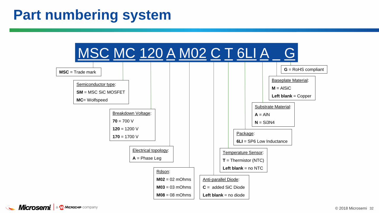
Part numbering system
MSC MC 120 A M02 C T 6LI A GMSC = Trade mark
Semiconductor type:
SM = MSC SiC MOSFET
MC= Wolfspeed
Breakdown Voltage:
70 = 700 V
120 = 1200 V
170 = 1700 V
Rdson:
M02 = 02 mOhms
M03 = 03 mOhms
M08 = 08 mOhms
Temperature Sensor:
T = Thermistor (NTC)
Left blank = no NTC
Substrate Material:
A = AlN
N = Si3N4
G = RoHS compliant
Package:
6LI = SP6 Low Inductance
Anti-parallel Diode:
C = added SiC Diode
Left blank = no diode
Electrical topology:
A = Phase Leg
Baseplate Material:
M = AlSiC
Left blank = Copper
33© 2018 Microsemi
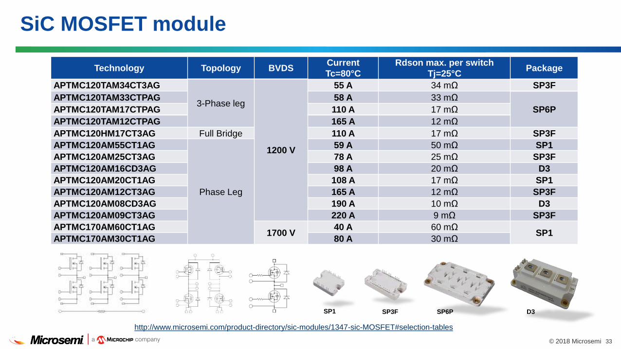
SP1 SP3F SP6P D3
SiC MOSFET module
Technology Topology BVDSCurrentTc=80°C
Rdson max. per switch Tj=25°C
Package
APTMC120TAM34CT3AG
3-Phase leg
1200 V
55 A 34 mΩ SP3FAPTMC120TAM33CTPAG 58 A 33 mΩ
SP6PAPTMC120TAM17CTPAG 110 A 17 mΩ
APTMC120TAM12CTPAG 165 A 12 mΩ
APTMC120HM17CT3AG Full Bridge 110 A 17 mΩ SP3FAPTMC120AM55CT1AG
Phase Leg
59 A 50 mΩ SP1APTMC120AM25CT3AG 78 A 25 mΩ SP3FAPTMC120AM16CD3AG 98 A 20 mΩ D3APTMC120AM20CT1AG 108 A 17 mΩ SP1APTMC120AM12CT3AG 165 A 12 mΩ SP3FAPTMC120AM08CD3AG 190 A 10 mΩ D3APTMC120AM09CT3AG 220 A 9 mΩ SP3FAPTMC170AM60CT1AG
1700 V40 A 60 mΩ
SP1APTMC170AM30CT1AG 80 A 30 mΩ
http://www.microsemi.com/product-directory/sic-modules/1347-sic-MOSFET#selection-tables
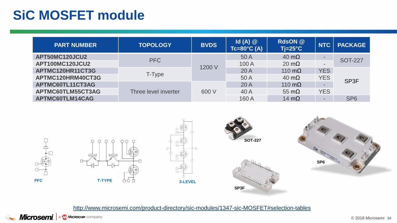
34© 2018 Microsemi
T-TYPE 3-LEVEL
PART NUMBER TOPOLOGY BVDSId (A) @
Tc=80°C (A)RdsON @ Tj=25°C
NTC PACKAGE
APT50MC120JCU2PFC
1200 V
50 A 40 mΩ -SOT-227
APT100MC120JCU2 100 A 20 mΩ -APTMC120HR11CT3G
T-Type20 A 110 mΩ YES
SP3FAPTMC120HRM40CT3G 50 A 40 mΩ YESAPTMC60TL11CT3AG
Three level inverter 600 V20 A 110 mΩ -
APTMC60TLM55CT3AG 40 A 55 mΩ YESAPTMC60TLM14CAG 160 A 14 mΩ - SP6
PFC
http://www.microsemi.com/product-directory/sic-modules/1347-sic-MOSFET#selection-tables
SiC MOSFET module
SP3F
SOT-227
SP6
35© 2018 Microsemi
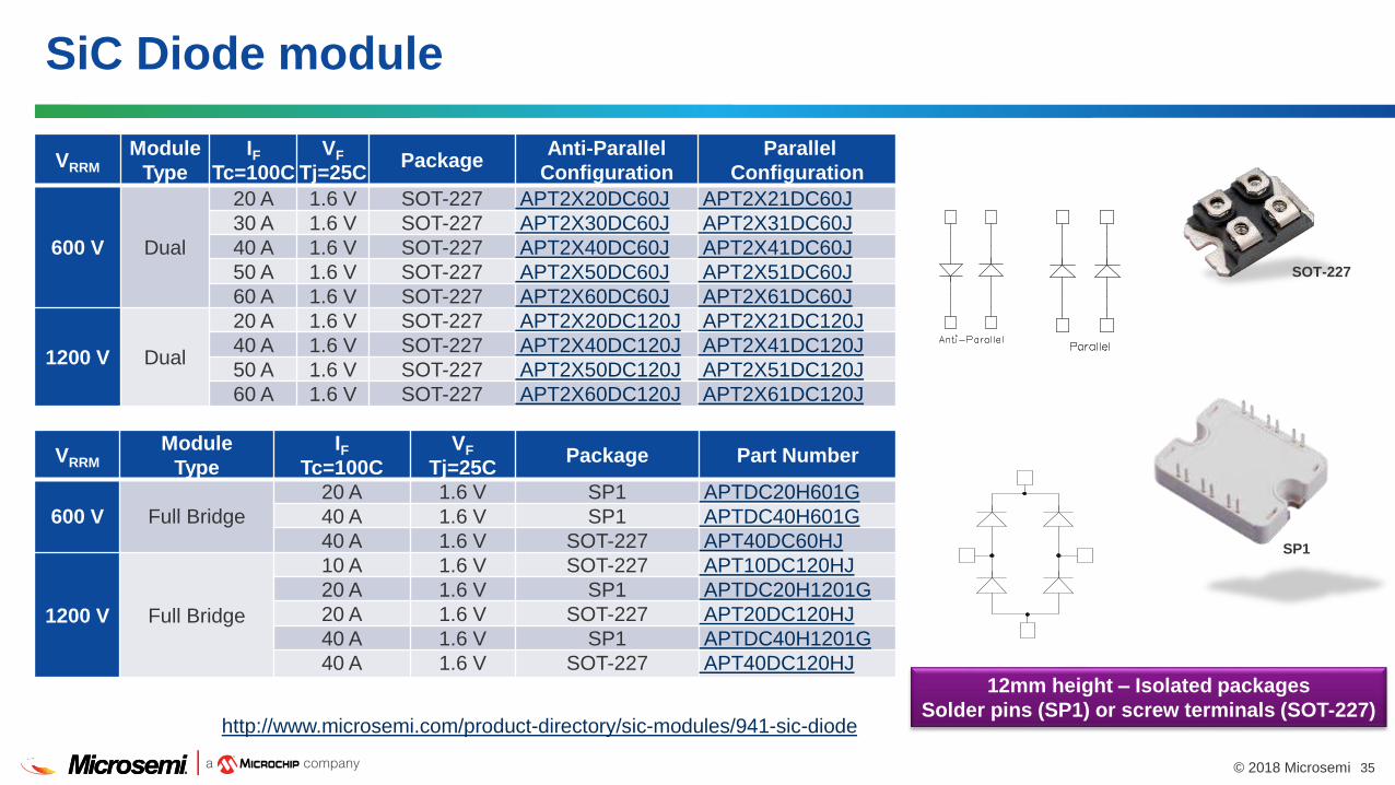
SiC Diode module
12mm height – Isolated packagesSolder pins (SP1) or screw terminals (SOT-227)
SOT-227
SP1
VRRMModule
TypeIF
Tc=100CVF
Tj=25CPackage
Anti-Parallel Configuration
Parallel Configuration
600 V Dual
20 A 1.6 V SOT-227 APT2X20DC60J APT2X21DC60J30 A 1.6 V SOT-227 APT2X30DC60J APT2X31DC60J40 A 1.6 V SOT-227 APT2X40DC60J APT2X41DC60J50 A 1.6 V SOT-227 APT2X50DC60J APT2X51DC60J60 A 1.6 V SOT-227 APT2X60DC60J APT2X61DC60J
1200 V Dual
20 A 1.6 V SOT-227 APT2X20DC120J APT2X21DC120J40 A 1.6 V SOT-227 APT2X40DC120J APT2X41DC120J50 A 1.6 V SOT-227 APT2X50DC120J APT2X51DC120J60 A 1.6 V SOT-227 APT2X60DC120J APT2X61DC120J
VRRMModule
TypeIF
Tc=100CVF
Tj=25CPackage Part Number
600 V Full Bridge20 A 1.6 V SP1 APTDC20H601G40 A 1.6 V SP1 APTDC40H601G40 A 1.6 V SOT-227 APT40DC60HJ
1200 V Full Bridge
10 A 1.6 V SOT-227 APT10DC120HJ20 A 1.6 V SP1 APTDC20H1201G20 A 1.6 V SOT-227 APT20DC120HJ40 A 1.6 V SP1 APTDC40H1201G40 A 1.6 V SOT-227 APT40DC120HJ
http://www.microsemi.com/product-directory/sic-modules/941-sic-diode
SiC gate driver boards
37© 2018 Microsemi
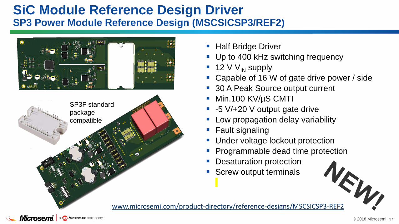
SiC Module Reference Design DriverSP3 Power Module Reference Design (MSCSICSP3/REF2)
Half Bridge Driver Up to 400 kHz switching frequency 12 V VIN supply Capable of 16 W of gate drive power / side 30 A Peak Source output current Min.100 KV/µS CMTI -5 V/+20 V output gate drive Low propagation delay variability Fault signaling Under voltage lockout protection Programmable dead time protection Desaturation protection Screw output terminals
SP3F standard package compatible
www.microsemi.com/product-directory/reference-designs/MSCSICSP3-REF2
38© 2018 Microsemi
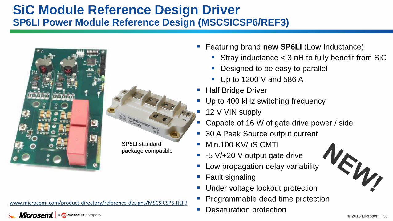
SiC Module Reference Design DriverSP6LI Power Module Reference Design (MSCSICSP6/REF3)
Featuring brand new SP6LI (Low Inductance) Stray inductance < 3 nH to fully benefit from SiC Designed to be easy to parallel Up to 1200 V and 586 A
Half Bridge Driver Up to 400 kHz switching frequency 12 V VIN supply Capable of 16 W of gate drive power / side 30 A Peak Source output current Min.100 KV/µS CMTI -5 V/+20 V output gate drive Low propagation delay variability Fault signaling Under voltage lockout protection Programmable dead time protection Desaturation protection
www.microsemi.com/product-directory/reference-designs/MSCSICSP6-REF3
SP6LI standard package compatible
39© 2018 Microsemi
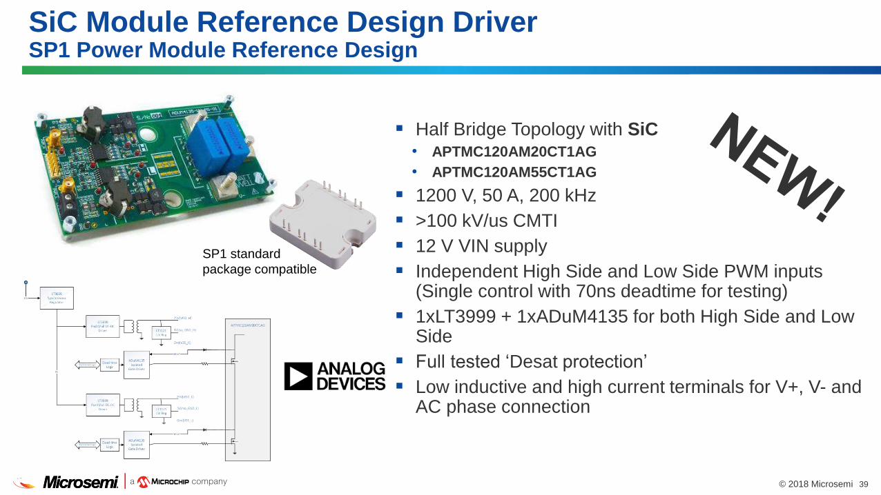
Half Bridge Topology with SiC• APTMC120AM20CT1AG • APTMC120AM55CT1AG
1200 V, 50 A, 200 kHz >100 kV/us CMTI 12 V VIN supply Independent High Side and Low Side PWM inputs
(Single control with 70ns deadtime for testing) 1xLT3999 + 1xADuM4135 for both High Side and Low
Side Full tested ‘Desat protection’
Low inductive and high current terminals for V+, V- and AC phase connection
SiC Module Reference Design DriverSP1 Power Module Reference Design
SP1 standard package compatible
Aerospace Integrated Power Solutions
41© 2018 Microsemi
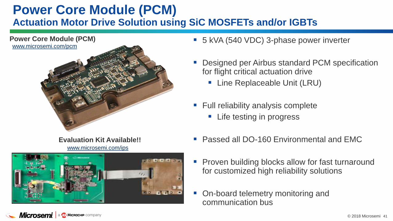
Power Core Module (PCM)Actuation Motor Drive Solution using SiC MOSFETs and/or IGBTs
5 kVA (540 VDC) 3-phase power inverter
Designed per Airbus standard PCM specification for flight critical actuation drive Line Replaceable Unit (LRU)
Full reliability analysis complete Life testing in progress
Passed all DO-160 Environmental and EMC
Proven building blocks allow for fast turnaround for customized high reliability solutions
On-board telemetry monitoring and communication bus
Evaluation Kit Available!!
www.microsemi.com/pcmPower Core Module (PCM)
www.microsemi.com/ips
42© 2018 Microsemi
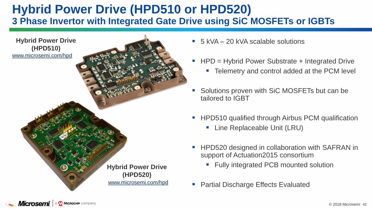
Hybrid Power Drive (HPD510 or HPD520)3 Phase Invertor with Integrated Gate Drive using SiC MOSFETs or IGBTs
5 kVA – 20 kVA scalable solutions
HPD = Hybrid Power Substrate + Integrated Drive Telemetry and control added at the PCM level
Solutions proven with SiC MOSFETs but can be tailored to IGBT
HPD510 qualified through Airbus PCM qualification Line Replaceable Unit (LRU)
HPD520 designed in collaboration with SAFRAN in support of Actuation2015 consortium Fully integrated PCB mounted solution
Partial Discharge Effects Evaluated
Hybrid Power Drive (HPD520)
Hybrid Power Drive (HPD510)
www.microsemi.com/hpd
www.microsemi.com/hpd

43© 2018 Microsemi
Microsemi, a wholly owned subsidiary of Microchip Technology Inc. (Nasdaq: MCHP), offers a comprehensive portfolio of semiconductor and systemsolutions for aerospace & defense, communications, data center and industrial markets. Products include high-performance and radiation-hardenedanalog mixed-signal integrated circuits, FPGAs, SoCs and ASICs; power management products; timing and synchronization devices and precise timesolutions, setting the world's standard for time; voice processing devices; RF solutions; discrete components; enterprise storage and communicationsolutions, security technologies and scalable anti-tamper products; Ethernet solutions; Power-over-Ethernet ICs and midspans; as well as custom designcapabilities and services. Learn more at www.microsemi.com.
Microsemi makes no warranty, representation, or guarantee regarding the information contained herein or the suitability of its products and services for any particular purpose, nor does Microsemiassume any liability whatsoever arising out of the application or use of any product or circuit. The products sold hereunder and any other products sold by Microsemi have been subject to limitedtesting and should not be used in conjunction with mission-critical equipment or applications. Any performance specifications are believed to be reliable but are not verified, and Buyer must conductand complete all performance and other testing of the products, alone and together with, or installed in, any end-products. Buyer shall not rely on any data and performance specifications orparameters provided by Microsemi. It is the Buyer’s responsibility to independently determine suitability of any products and to test and verify the same. The information provided by Microsemihereunder is provided “as is, where is” and with all faults, and the entire risk associated with such information is entirely with the Buyer. Microsemi does not grant, explicitly or implicitly, to any partyany patent rights, licenses, or any other IP rights, whether with regard to such information itself or anything described by such information. Information provided in this document is proprietary toMicrosemi, and Microsemi reserves the right to make any changes to the information in this document or to any products and services at any time without notice.
©2018 Microsemi, a wholly owned subsidiary of Microchip Technology Inc. All rights reserved. Microsemi and the Microsemi logo are registered trademarks of Microsemi Corporation. All othertrademarks and service marks are the property of their respective owners.
Microsemi HeadquartersOne Enterprise, Aliso Viejo, CA 92656 USAWithin the USA: +1 (800) 713-4113Outside the USA: +1 (949) 380-6100Sales: +1 (949) 380-6136Fax: +1 (949) 215-4996email: [email protected]
Thank you!


![Diathermy Safety[1]](https://img.pdfslide.us/doc/110x75/543e9a49afaf9f195e8b4838/diathermy-safety1.jpg)