Embed Size (px)
Citation preview
Rapid On-Chip Electromagnetic
Extraction and Compact Modeling
with Guaranteed Passivity
Sotiris Bantas
Helic S.A.
MOS-AK/ESSDERC/ESSCIRC WorkshopAthens 18 Sep. 2009
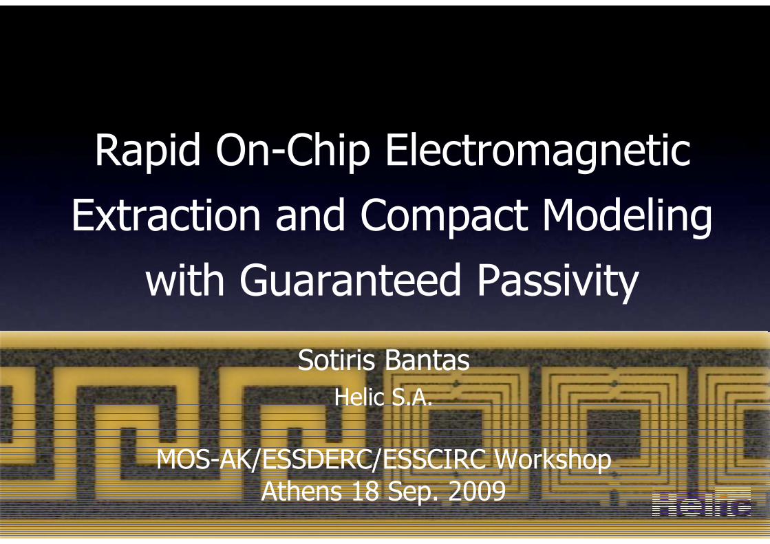
Motivation
� Verification of modern RF and high-speed IC requires electromagnetic (EM) models for passives, interconnects
� But traditional simulation methods (MoM, FEM) cannot handle the complexity
� Moreover, SPICE-compatible EM models are needed for circuit simulation
� EM models need to be compact for fast simulation, yet detailed and broadband
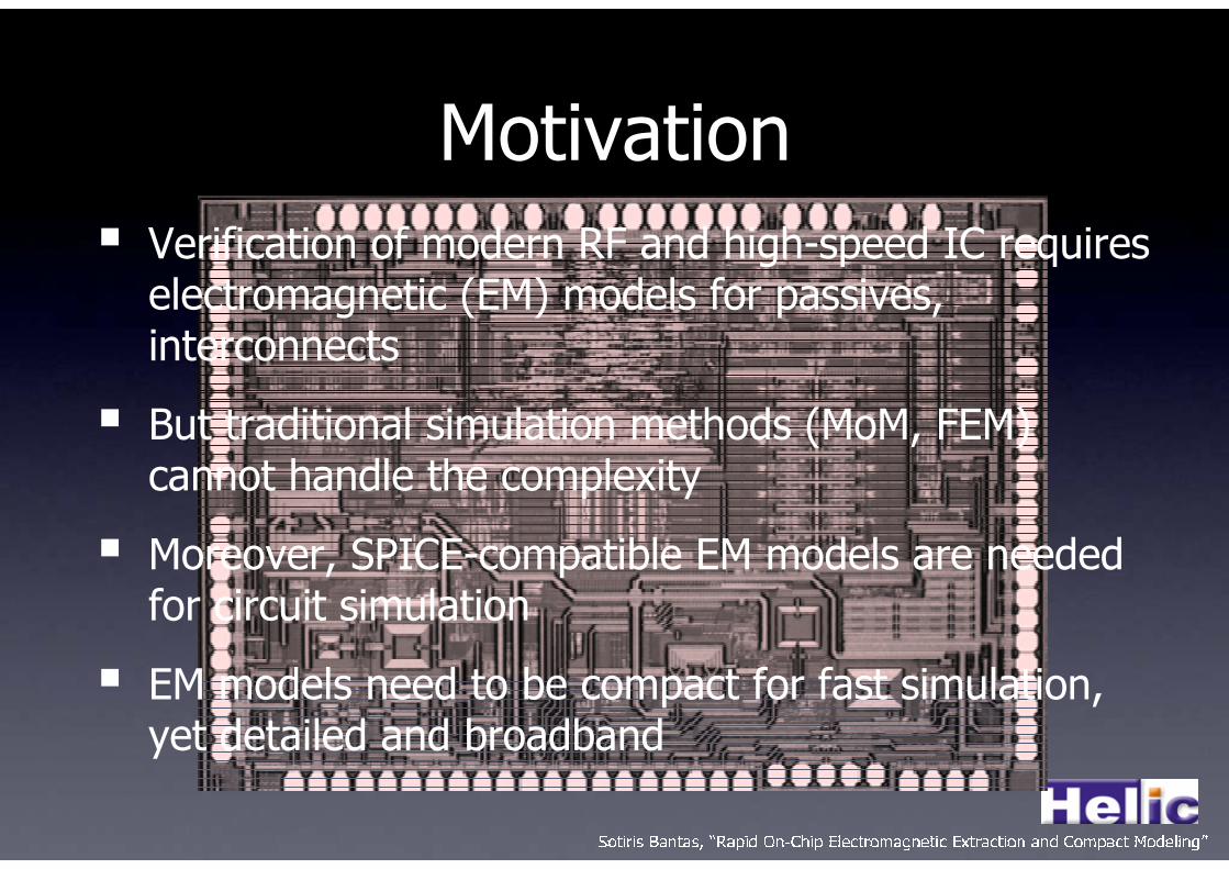
A short (biased) history…� E. B. Rosa, "The self and mutual inductance of linear conductors", Bulletin of the National Bureau of Standards, 1908.
� F. W. Grover, “Inductance Calculations”, 1946. (*)
� A. E. Ruehli, "Inductance calculations in a complex integrated circuit environment", IBM Journal of Research and Development, 1972.
� H. M. Greenhouse, “Design of planar rectangular microelectronic inductors”, IEEE Trans. Parts, Hybrids and Packaging, 1974. (*)
� K. Nabors, and J. K. White, “FASTCAP: a multipole accelerated 3-d capacitance extraction program”, IEEE Transactions on CAD of Integrated Circuits and Systems, 1991.
� Kamon, M. et al., “FASTHENRY: a Multipole Accelerated 3D Inductance Extraction Program”, IEEE Trans. Microwave Theory & Techniques, 1994.
� K. L. Shepard and Z. Tian, “Return-limited inductances: A practical approach to on-chip
inductance extraction,” in Proc. IEEE Custom Integrated Circuits Conf., 1999.
� Y. Koutsoyannopoulos, Y. Papananos, “SISP: A CAD Tool for Simulating the Performance of Polygonal and Multi-Layer Integrated Inductors on Silicon Substrates”, Int’l Conf. on VLSI and
CAD, 1997. (*)
� A. Devgan and H. Ji and W. Dai, "How to efficiently capture on-chip inductance effect: Introducing a new circuit element K", Proc. IEEE ICCAD, 2000.(*) Influenced this work.
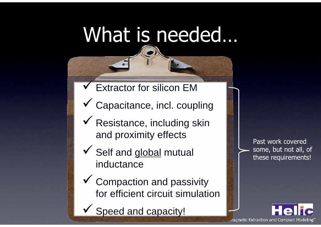
What is needed…
� Extractor for silicon EM
� Capacitance, incl. coupling
� Resistance, including skin and proximity effects
� Self and global mutual inductance
� Compaction and passivity for efficient circuit simulation
� Speed and capacity!
Past work covered some, but not all, of these requirements!
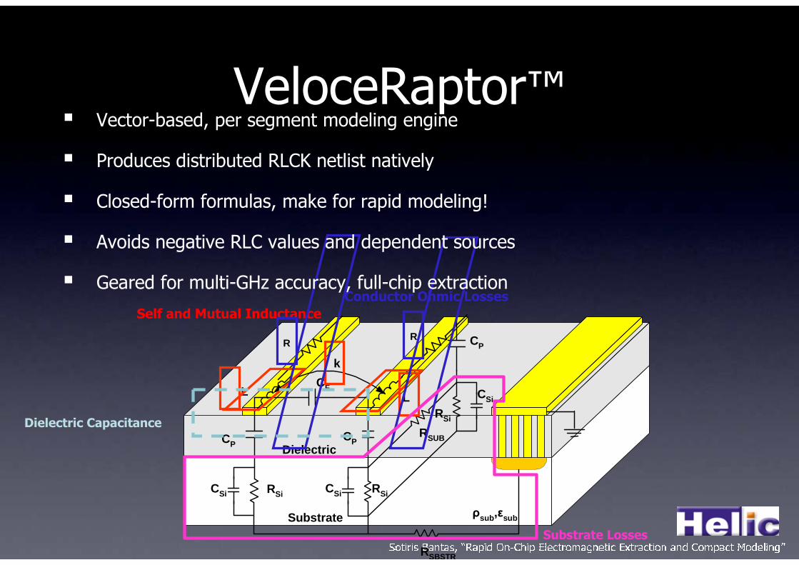
VeloceRaptor™
CPCP
ρsub,εsub
RSiCSi RSiCSi
Substrate
Dielectric
RSBSTR
L L
k
CP
CF
RSUB
CSi
RSi
RR
Self and Mutual Inductance
Conductor Ohmic Losses
Dielectric Capacitance
Substrate Losses
� Vector-based, per segment modeling engine
� Produces distributed RLCK netlist natively
� Closed-form formulas, make for rapid modeling!
� Avoids negative RLC values and dependent sources
� Geared for multi-GHz accuracy, full-chip extraction
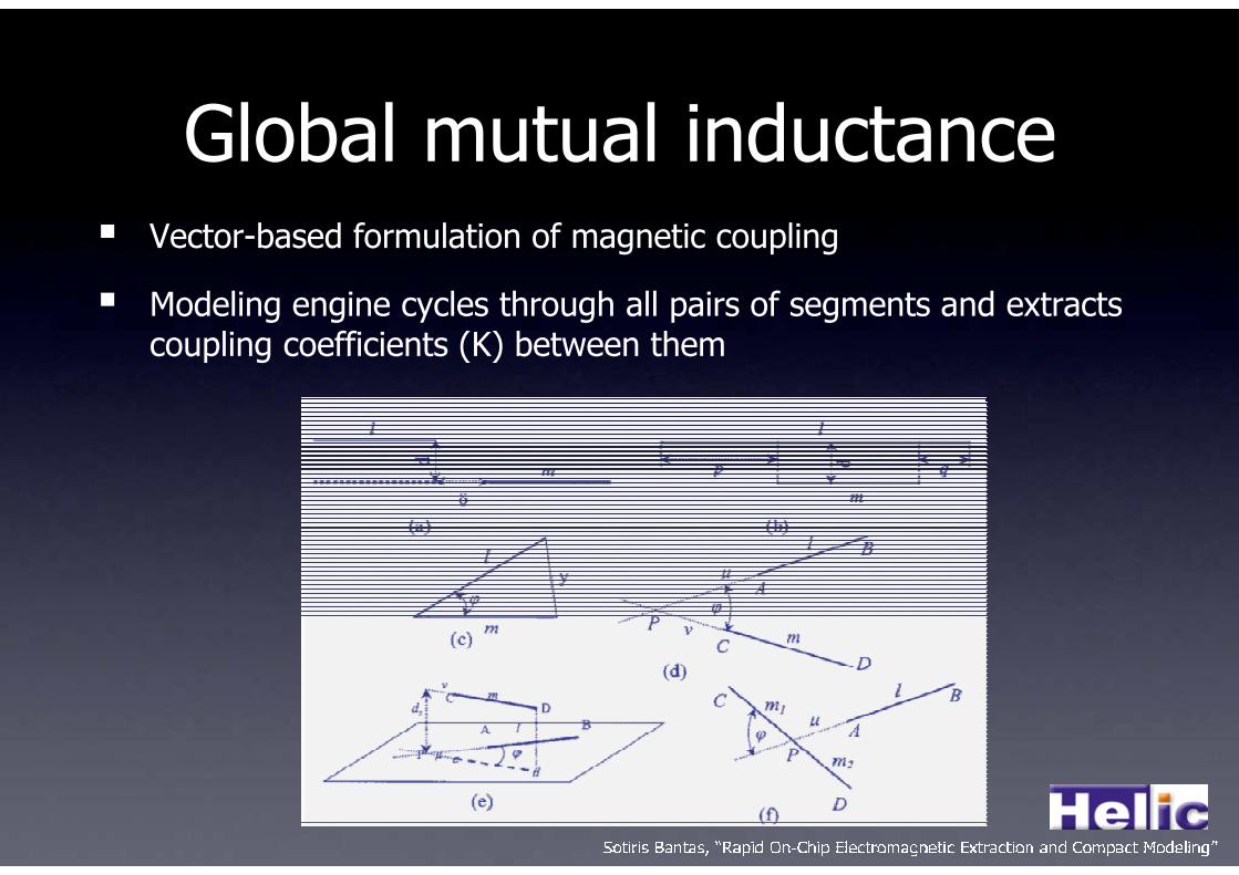
Global mutual inductance� Vector-based formulation of magnetic coupling
� Modeling engine cycles through all pairs of segments and extracts coupling coefficients (K) between them
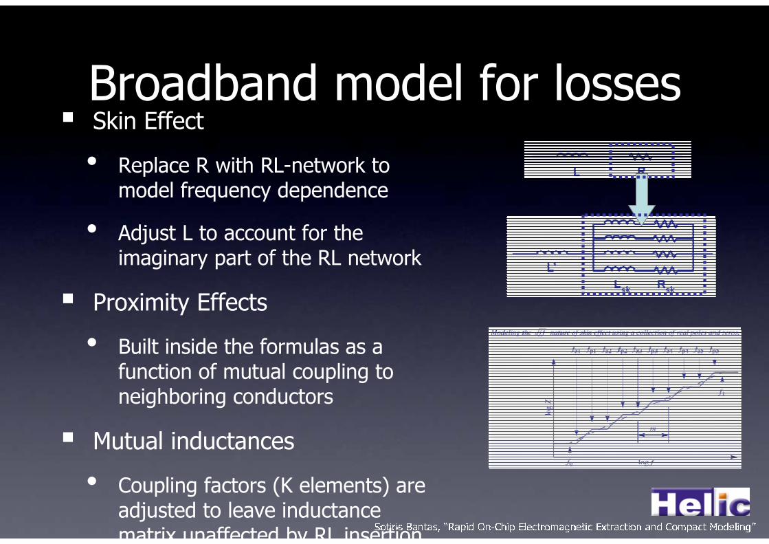
Broadband model for losses� Skin Effect
• Replace R with RL-network to model frequency dependence
• Adjust L to account for the imaginary part of the RL network
� Proximity Effects
• Built inside the formulas as a function of mutual coupling to neighboring conductors
� Mutual inductances
• Coupling factors (K elements) are adjusted to leave inductance matrix unaffected by RL insertion
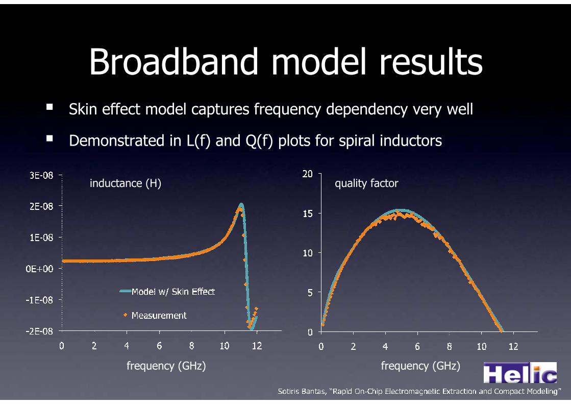
Broadband model results
frequency (GHz) frequency (GHz)
inductance (H) quality factor
� Skin effect model captures frequency dependency very well
� Demonstrated in L(f) and Q(f) plots for spiral inductors
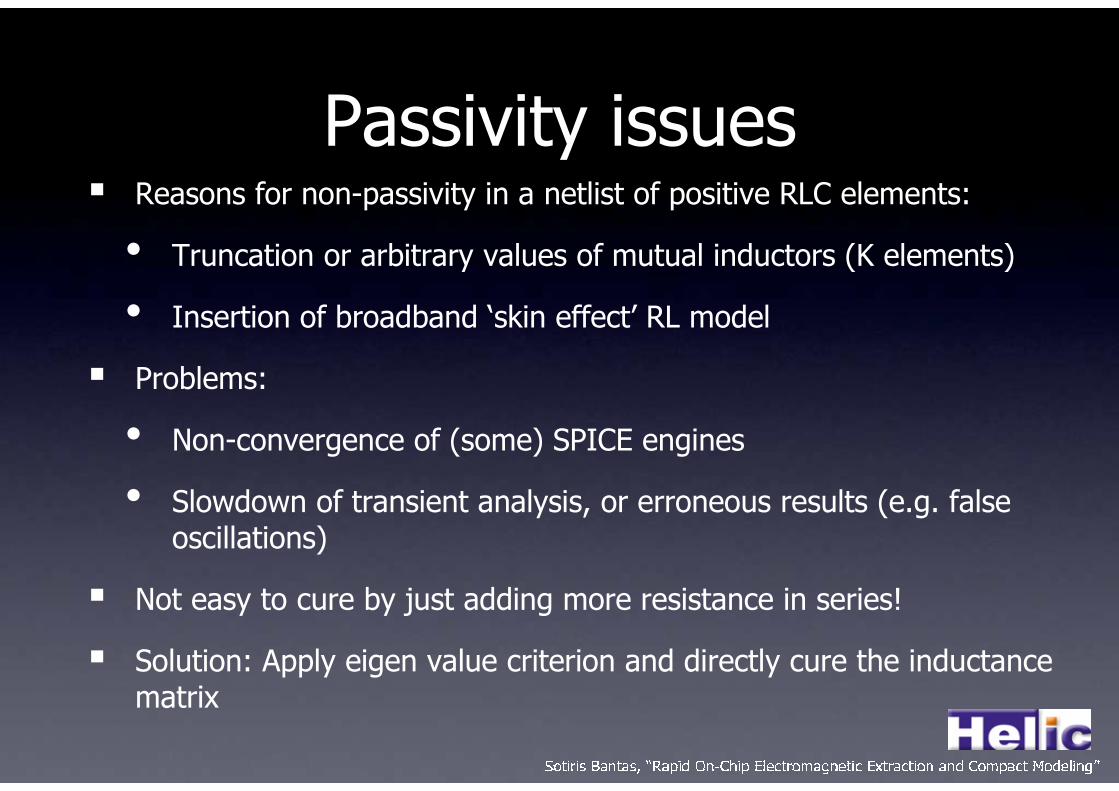
Passivity issues� Reasons for non-passivity in a netlist of positive RLC elements:
• Truncation or arbitrary values of mutual inductors (K elements)
• Insertion of broadband ‘skin effect’ RL model
� Problems:
• Non-convergence of (some) SPICE engines
• Slowdown of transient analysis, or erroneous results (e.g. falseoscillations)
� Not easy to cure by just adding more resistance in series!
� Solution: Apply eigen value criterion and directly cure the inductance matrix
L =
L self 1 M12 L M1N
M 21 L self 2 L M 2N
M M O M
M N1 M N 2 L L selfN
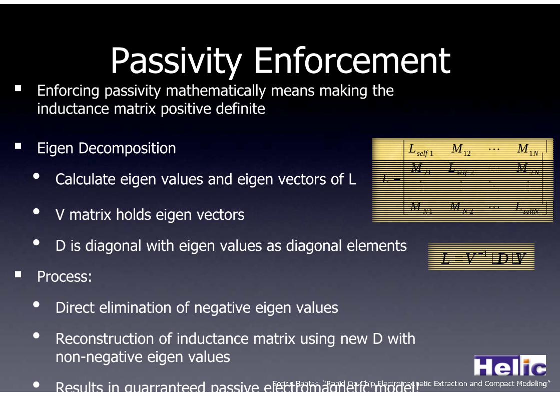
Passivity Enforcement � Enforcing passivity mathematically means making the
inductance matrix positive definite
� Eigen Decomposition
• Calculate eigen values and eigen vectors of L
• V matrix holds eigen vectors
• D is diagonal with eigen values as diagonal elements
� Process:
• Direct elimination of negative eigen values
• Reconstruction of inductance matrix using new D with non-negative eigen values
• Results in guarranteed passive electromagnetic model!
VDVL ⋅⋅= −1
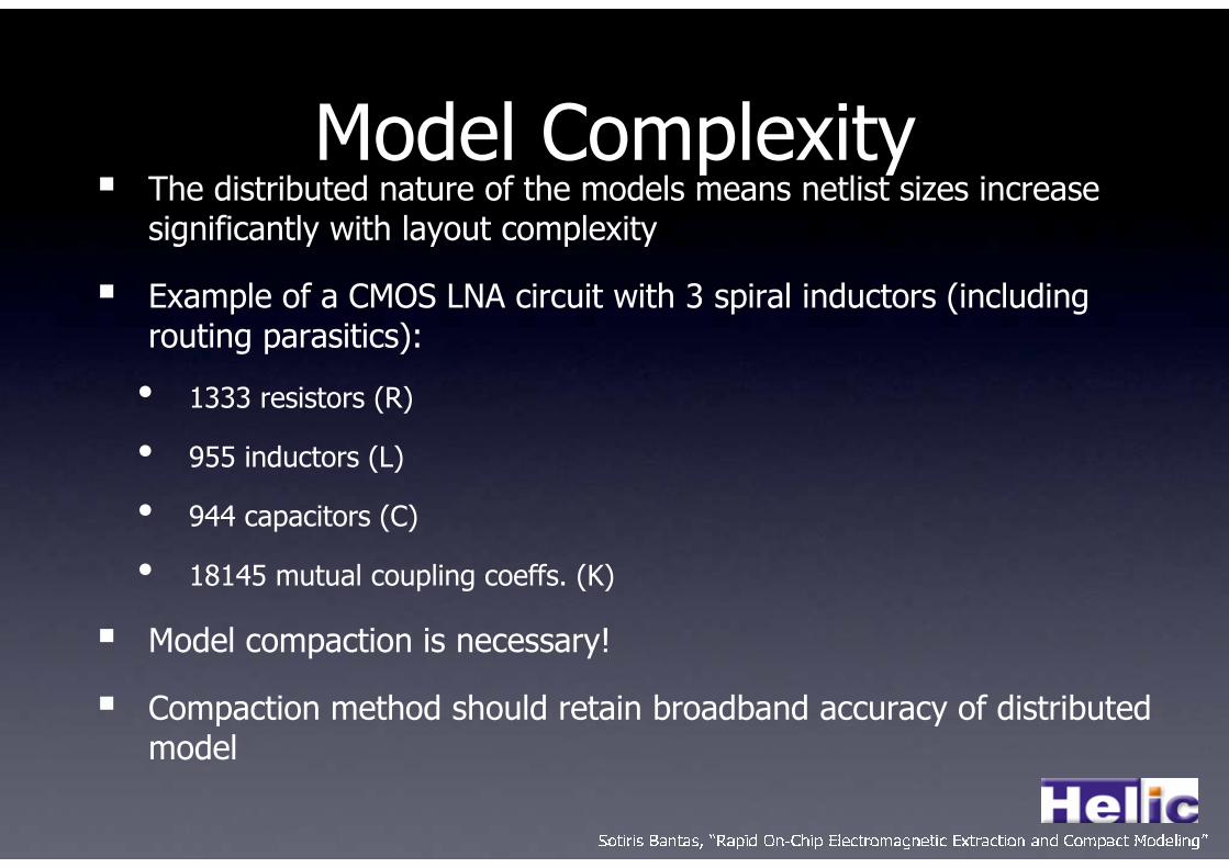
Model Complexity� The distributed nature of the models means netlist sizes increase
significantly with layout complexity
� Example of a CMOS LNA circuit with 3 spiral inductors (includingrouting parasitics):
• 1333 resistors (R)
• 955 inductors (L)
• 944 capacitors (C)
• 18145 mutual coupling coeffs. (K)
� Model compaction is necessary!
� Compaction method should retain broadband accuracy of distributed model
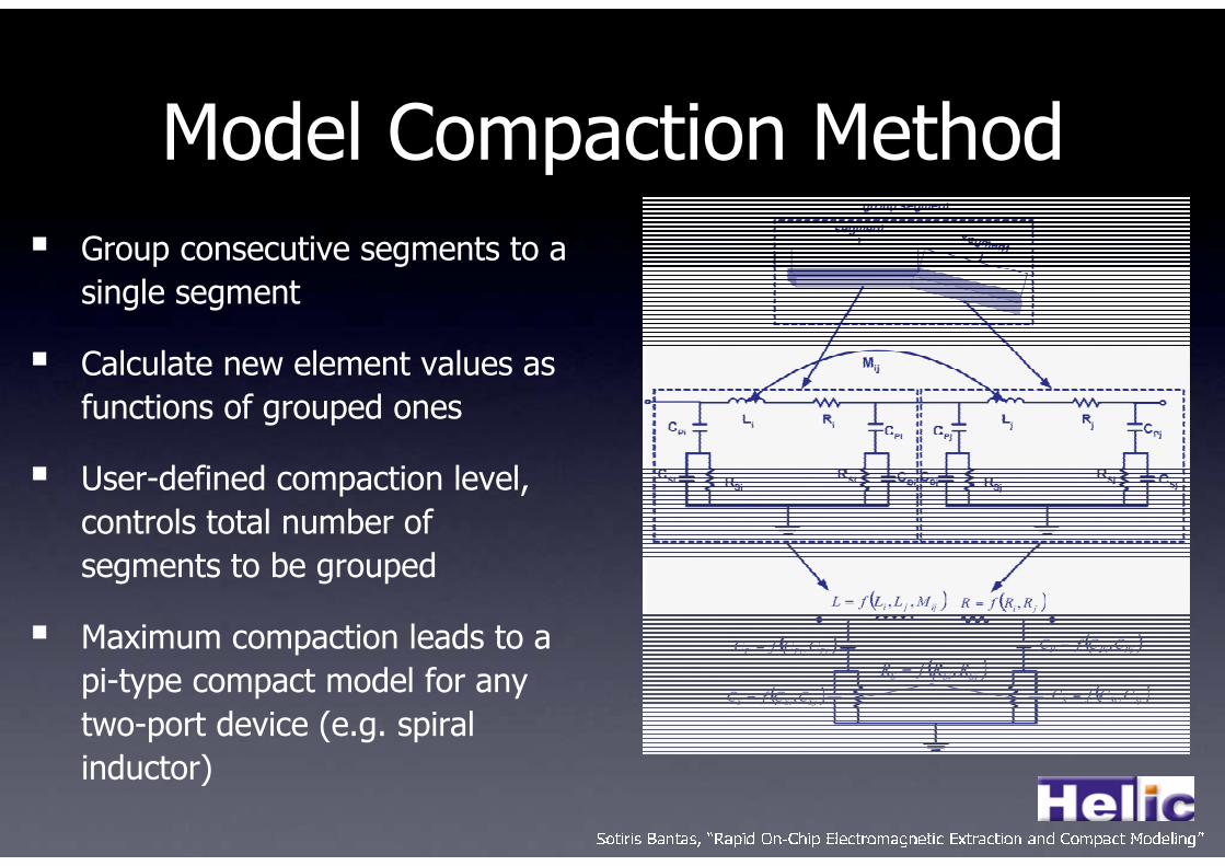
Model Compaction Method
� Group consecutive segments to a
single segment
� Calculate new element values as
functions of grouped ones
� User-defined compaction level,
controls total number of
segments to be grouped
� Maximum compaction leads to a
pi-type compact model for any
two-port device (e.g. spiral
inductor)
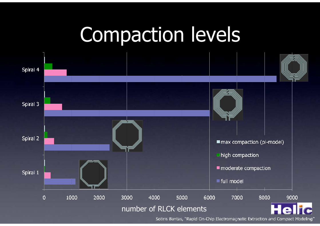
number of RLCK elements
Compaction levels
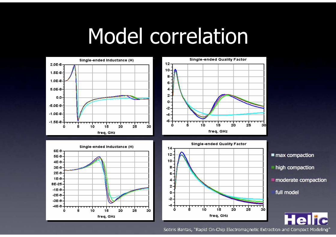
Model correlation
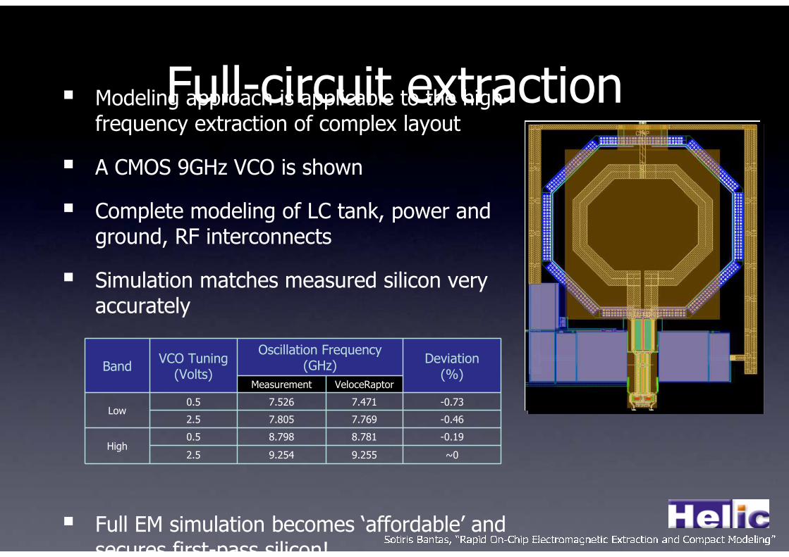
� Modeling approach is applicable to the high-frequency extraction of complex layout
� A CMOS 9GHz VCO is shown
� Complete modeling of LC tank, power and ground, RF interconnects
� Simulation matches measured silicon very accurately
� Full EM simulation becomes ‘affordable’ and secures first-pass silicon!
Full-circuit extraction
BandVCO Tuning(Volts)
Oscillation Frequency(GHz)
Deviation(%)
Measurement VeloceRaptor
Low0.5 7.526 7.471 -0.73
2.5 7.805 7.769 -0.46
High0.5 8.798 8.781 -0.19
2.5 9.254 9.255 ~0
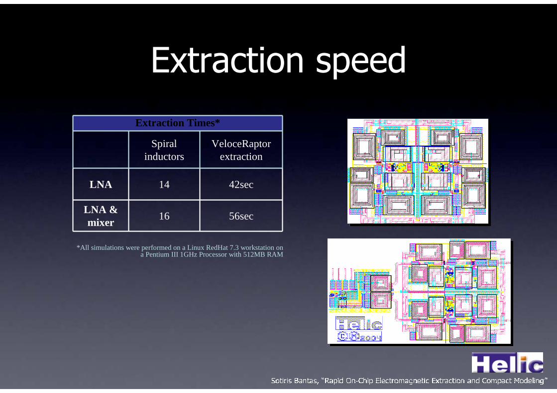
Extraction speed
Extraction Times*
Spiral inductors
VeloceRaptor extraction
LNA 14 42sec
LNA &mixer
16 56sec
*All simulations were performed on a Linux RedHat 7.3 workstation on a Pentium III 1GHz Processor with 512MB RAM
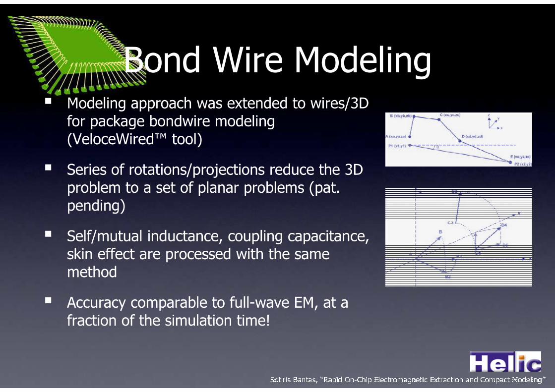
Bond Wire Modeling� Modeling approach was extended to wires/3D
for package bondwire modeling (VeloceWired™ tool)
� Series of rotations/projections reduce the 3D problem to a set of planar problems (pat. pending)
� Self/mutual inductance, coupling capacitance, skin effect are processed with the same method
� Accuracy comparable to full-wave EM, at a fraction of the simulation time!
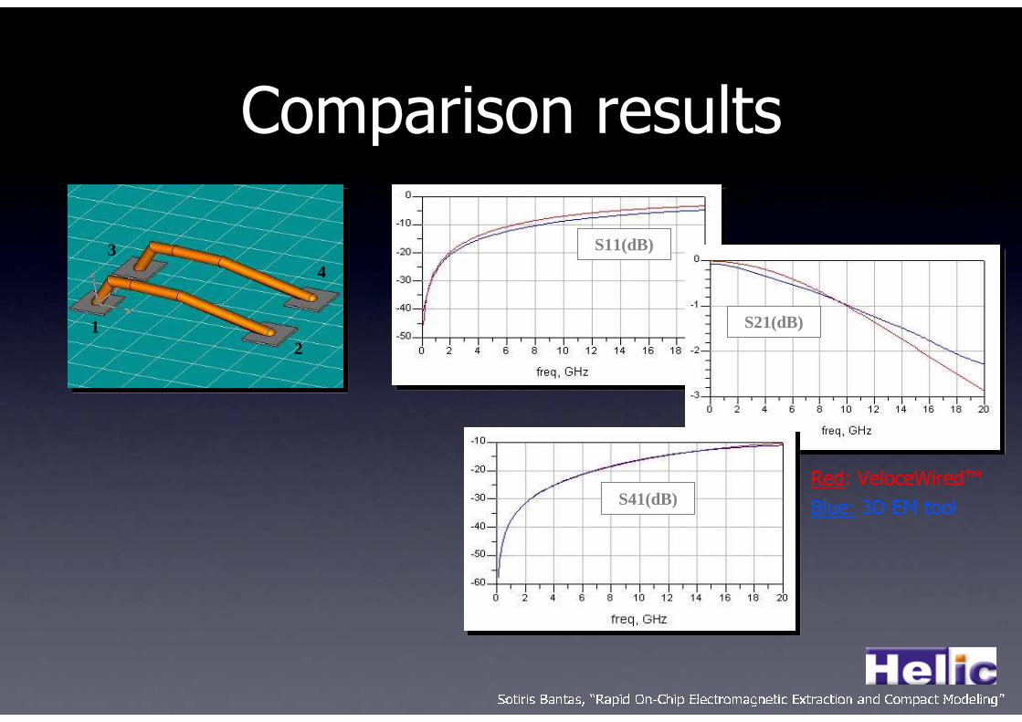
Comparison results
Red: VeloceWired™
Blue: 3D EM tool
S11(dB)
S21(dB)
S41(dB)
12
34
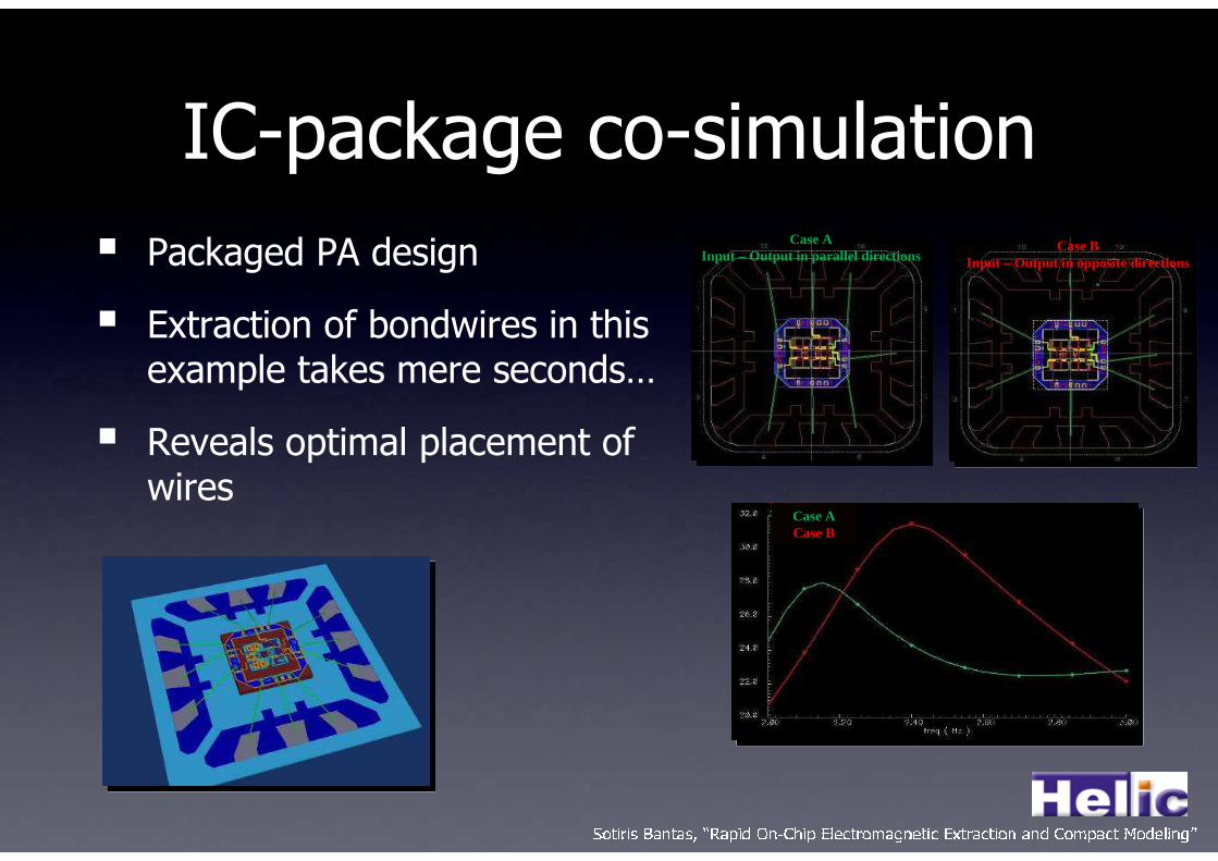
IC-package co-simulationCase B
Input – Output in opposite directions
Case A Input – Output in parallel directions
Case A Case B
� Packaged PA design
� Extraction of bondwires in this example takes mere seconds…
� Reveals optimal placement of wires
Conclusions� A complete methodology was presented for the rapid, yet accurate, EM modeling of ICs and packages
� Models are broadband and capture global magnetic coupling effects
� Passivity is ensured for efficient circuit simulation
� Model compaction level is controllable
� Extraction of complex RF & high-speed ICs for EM effects is now possible, practical and fast
![Microfluidics Photomask Design using AutoCAD software for ... · microfluidics structure for DNA extraction on a single chip in a biosensor forms a lab-on-a-chip (LOC) device [9],](https://img.pdfslide.us/doc/110x75/5f2b2153c9346e1bff11a58d/microfluidics-photomask-design-using-autocad-software-for-microfluidics-structure.jpg)