Embed Size (px)
Citation preview
bullbull bull
t 3 6 J - 21 4f l 9 middot~ r Oa E EI(r J rl ikh S~ lrr~a =Jrer ng
wwwaefse 3670 ~~------------------------~------------------------
r e ca r
4416
Response Test Unit
val id from serial no 5 7 5 44 3
037-261
BRUEL amp KJAR NaJrum - Denmark Service Instruction 4416
4416
Response Test Unit
valid from serial no 575443
037- 261
Consisting of
Service Instruction Simplified Di agram
AdluSlmenl Procedure
ZS 0298 Rem ote Coniroi
ZT 0294 Ampllfier Powe r Supply
ZT 0295 Inpul Filter
Circuit Diagram with Parts Lisl Cablnet Part s
Page Dale
0-- 1 4 76 0--2 4 76
1-1 4 76 1shy 2 476 1shy 3 476 1shy 4 4 76
76
1 76 2 76
76
2-1 1 76
Trouble Shooting
If any faults should occur please check Ihe inslrumenl accordlng 10 Ihe Adjustment Procedure
When a faull has been Iraced and corrected the vollages and adjuslments influenced by Ihe correclion muSI be rechecked The complete instrument should then be tesled to make sure Ihal all basic funclions are operative
The tolerances given In these notes are Intended for use as guide for adshyjustments
Before correcting any apparent deviation make sure thal the measuring instrument has tolerances small enough not to aflect Ihe measuremenl
Modifications
Due to the constant technical progress the Instrument will be modilied from time to time in order to provide continously improved performance
For this reason there may be small differencies between the instrumenl and the Service Instruction
However the local Representative Service is in possession of all informashytion regarding the modifications that have been made
Spare Parts
Please state type and serial number 01 the instrument when ordering spare parts
4 76 0--1
Amplifier (J) N 3
Preamp 10 mY -O
Zi 17 kfi Rumble = iii
A 8 a LP 315 Hz BP 315 Hz ----shy O
Vll OJ ltO
OJ
3 -r ~f-J~ Input 100 mY 1Hz Chopper ffi p
Tope
tfm ~
R f J I EC + Boost 75)s
100 mV10 mV
5 V Input
Lr 5 V
to V 11middotIs
b--+--IR
I I
I
-- to V 13 R8~ 5 V L+R ~ ~ to V12 _ loQ8 9
I I 5 V Chop O----------
Aumble A f T middotIs
to V 23
Aumb le B -o I t TI ~s
~
-J ffi
Out
~
-J ~ W ZDJN
Z () ffi
Gl ~ ~O r -O -oomCD Ogt coo (i (icao mi tl Co 3 r tl - )-tD ~ () ~
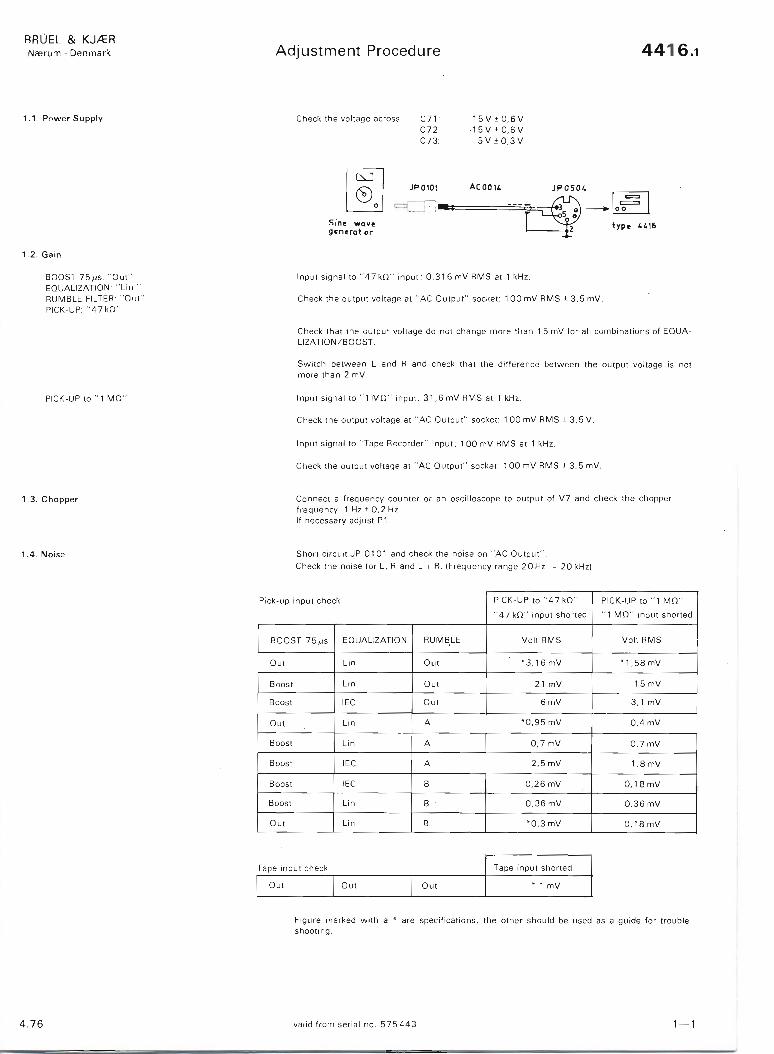
BROEL amp KJttR Nrerum - Denmark Adjustment Procedure 44161
11 Power Supply Check the vo ltage across C71 C72 C73
15V 06V -15Vplusmn06V
5Vplusmn03V
Sine wave gonerat or
12 Gain
BOOST 75Jjs Out EOUALlZATIO N Lin RUMBLE FILTER Out PICK-UP 47kO
Input signa l to 47 kO input 0316 mV RMS at 1 kHz
Check the outp ut voltage at AC Output socket 1 00 mV RMS plusmn 3 5 mV
Check that the output vo ltage do not change more than 15 mV for all combinations of EOUAshyLlZATION BOOST
Switch between more than 2 mV
L and R and check that the difference between the output voltage is not
PICK-UP to 1 MO In put signal to 1 MO input 316 mV RMS at 1 kHz
Check the output voltage at AC Output socket 100 mV RMS plusmn35 V
Input signal to Tape Recorder input 100 mV RMS at 1 kHz
Check the ou tput voltage at AC Output socket 100 mV RMS plusmn 35 mV
1 3 Chopper Connect a frequency counter frequency 1 Hz plusmn 0 2 Hz If necessary adj ust P 1
or an oscilloscope to output of V7 and check the chopper
1 4 Noise Short cirCulI Jp 0101 and check the noise on AC Output
Check the noise for L R and L + R (Frequ ency range 20 Hz - 20 kHz)
Pick-up inpu t check PICK -UP to 47 kO
47 kO input shorted
PICK-UP to 1 MO
1 MO Input shorted
BOOST 75Jjs EOUALlZATION RUMBLE Volt RMS Volt RM S
Out Lin Out bull 316 mV 1 58mV
Boost
Boost
Lin
IEC
Out
Out
21 mV
6mV
15mV
3 1 mV
Out
Boost
Boost
Lin
Lin
IEC
A
A
A
095 mV
07mV
25mV
0 4mV
07 mV
18mV
Boost
800st
Out
IEC
Lin
Lin
8
B
8
026 mV
036 mV
03 mV
0 18mV
0 36 mV
0 18 mV
Tape input check
I Out I Out I Out
Tap e input shorted
il 1 mV
Figure marked with shooting
a bull are specifications the othe r should be used as a guide for trouble
476 valid from seria l no 575443 1-1
Adjustme nt Procedure 4416 1
15 Distortion Check the distortion for L R and L + R according to the scheme belove
The distortion should be measured with an output voltage of 1 V RMS 17 Rum
Tape in put 20Hz-20kHz lt 70dB
IEC BOOST 5 Hz - 50kHz lt 60dB Pick-up inpul
LINBOOST 5 H z - 50 kHz lt 50dB
Rmote C ontrol
l AQ 0038
rom AC Output EOU f CHAI
2307 UB 0041 RUM 2010
Il 4416 to AC volt meter 2 1nput 3 1 O J (f inst2427)
RUM Zi 47kJl
I BFO I Output RUM
To check item 1 6 and 1 7 a Level Recorder and a Si ne Wave genera tor (frequ ency range 2 Hz - 200 kHz) is necessary
Th e w riting width o f the Le ve l Record er is 00 mm 1 8 Max
EOUI RUM
1 6 Frequency Response
- Bruel amp Kjr Bruel amp Kjcer Brii e I amp Kjmr 00000000000000000000000000 O O 00000000000000000000 O
Bruelamp Kjrer Potentiometer Rnge ~dB Rectiier RMS Lower Lim Freq ~HzWr Speed ~mmsec Paper Speed~mmsec Capen hagen 50 25 1075
1 Lin 1 9 Cross- dBdB 2 Lin + Boost 75 J1S dBdB
3 IEC 2+ EOW 4020 8 604 IEC + Boost 75 J1s CHM
3 amp 4-I--Measuring Obj PICKmiddot
30 15 f- ~45 Responsemiddot curves
2LIY p_e_ _ 4416 t=~ 1 amp2 1 amp4
2010 430
3 10-5 2 15
100 kHz Rec No Date 27middot6middot75 Sign JAH O O
10 20 Hz 50 100 200 500 1000 2000 5000 10000 200~00 A B C lin~ O PICK middot
OP 1124 C gt50634Multiply Frequency Scale by lero level 16122112 A 8
RUMBLE FI LTER Out Set the freq uency to 10H z in 2 Hz - 2 kHz log frequency range
Input vo ltag e to 47 kO input 0316 mV RMS Knob se tting for Type 2307
Start the Leve l Recorder and let it run until approximalely 1 kHz Stop the Level Recorder
LOWER LIMIT FREO 10Hz change the frequency rang e of the generator to 200 Hz - 200 kHz and se t the frequency
WRITING SPEED 16 mm pointer to the frequency wh ere it w as stopped Start the Level Recorder and let it run out the rest of the chartPAPER SPEED mm
Th is check should be done for L R L + R and for both 47 kOl l MO inpu ts
1-2 476 4 76
Adjustment Procedure 4416 1
17 Rumble Filter
Bruel amp Kj re r bull Me asuring Object Bruel amp Kjrer o o O o O O O o O o o o o o o o o O O o O O O O o O 00 O 00 O O 00 O O O O O O O O O O O O O O [
dB Recordi ng N o Sign Date Potentiometer Zera Level O A B C lin 5
plusmn 1 elB
40 Rumble A
Rumb le B JO
20
10
O 2 z lU O 50 100 200 500 1000 2000 5000 ~10000 2 0000 50000 100000
OPl143 Pot Range 50 dB Re ctifier RMS lower lim Freq 2 Hz Writing Speed 25 mm see Paper Speed 3 mm seco
EOUALlZATION Lin Adjust the input vol tag e to exactly 1 V RMS at 315Hz on AC Outpu t CHANNEL SELECTOR L + R RUMBLE FILTE R Out
RUMBLE FILTER to A Output voltage 1 V RMS plusmn 20 mV
RUMBLE FILTER to B Output voltage 1 V RMS plusmn 20 mV
Record the frequ ency response for RUMBLE A and RUMBLE B filters
1 8 M ax Output Voltage
EOUALlZATIO N Lin Connecl an oscilloscape lO AC Output socket and check that Ihe oulput signal is not disshyRUMBLE FILTER Out tored for an input vo ltage of 23 mV RMS to 47 kO inpUI
23 V RMS to 1 MO input
Check max outpu t vol tage for L R L + R and for bo th 47 kO and 1 MO inputs
1 9 Cross talk
EOUALlZING Lin ConneCllhe input signal to pin 3 and short circuit pin 5 to ground on 47 kO mput CHANN EL SELE CTOR R Adjust the input signal to 3 16 V RMS al 1 kHz on AC outpul PICK-UP 47 kO
Switch CHANN EL SELE CTOR lO L and check the cross lalk acord ing lO Ihe scheme below
Pi ck -upInput Tape frequency 47 kO 1 MO
o 1 kHz -65 dB -6 5 dB - 65 dB
20 kHz -45 dB - 4 0 dB -45 dB
50 kHz -35 dB -30dB - 35 dB
Change the mput lO channe l L and check the cross lalking
PICK-UP to 1 MO Change Ihe input signal lO 1 MO input and check the cross talk as described for 4 7 kO input
Change the inpul signal to Tape inpul and check Ihe CrOSS talk as described for 47 kO inpul
4 76 valid from serial no 57 5443 1-3
I
---- --
---------- - ------
BR UEL I Adjustment Procedure 4416 1 Noerum shy
1 10 Synchrosta rt er
Level Recorder type 2307 I
I I
StortStop Remote I
flip-flop Control ~ shyI o I
~----~
I
I I I I I
-~
Level Recorder type 2305
Remote Controi
I
~ to Remote Control
type 4416 Remot Control Cable
AQ 0039
Letllt Rero-def gart = av 30V fro l~y~ flectTilr
Single __ Chart
om G Automotic Stop
030215 VClutch
C 3ClS
EQUALlZING lin Connect Remote Contro i on Type 4416 to Remote Cont rol on the Leve l Re corder
CHA NNEL SELECTOR L + R RUMBLE FILTER Out Adjust the input signal for 100 mV RMS at 950 Hz on AC Output
PICK-UP 47 kO SYNCHROSTART Au SWllch PAPER DRIVE FUNCTION on Type 2307 to Continue F r-shy
l e
~ Press BFO Stop on Type 2010 and check that the Level Recorder starts
If the Level Recorder does not start ad just L301 (on ZS 0298) until th e relay 0301 w ill be energiled and repeat the check
Change the input frequency to 1050 Hl and check again the start function
If the Level Recorder does not start adjust L301 until the relay 0301 wi ll be energized and I repeat the stan function
Change the input frequency to 700 Hl and let the Level Recorder run unlil automatic stop
Increase the input frequency slow ly and check thaI the re lay wi ll be energiled between 800 Hl and 950 Hz and the Level Recorder will be starled between 1050 Hz and 1250 Hz
Repeat the adjustment of L301 until this is fullfilled
-eJshyR3u
1-4 4 76 176
BRUEL amp KJA R Nlterum - Denmark Circuit and Layout Diagrams ZS 0298
with Parts List Remote Controi
Remote Controi IN 41 43
Ol OJ
INC l411
Q]02
+ 15V HI e JD S
560kn JQk() AJ02 AJ 03
f------v ~ ]J ilF 4 h O
~~ AiI--4--H Ih o AJOS
I GNO 0---------------~--------1_----------~----~------~~--------L---~~ i
II
~ ~
0302 303 0301 V301302-BC107B1 J
o o 40 01o
6 o 0-~ SO 02 s S 60 03
6 6110111 ~ICw
80 o
CIRCUIT COMPONENT TYPE STOCK DIAGRAM REF REF
r--- -- ------o ()) 0 1 e 301 Polyeste r 33 nF 400 V es 0058
l () e 302 10 nF 250 V es 0403I a+o1f-1l~- II) I c 303 Polystyren e 01 JlF 63 V eT 1543
I be 1 R ~I I 1-1 11)1 e 304 Polyester 01 JlF 250 V es 0402
e 305-307 Electrolyti c 2 2JlF 63V CE 0401I ur I gtlt I l I
and L 301 Resonance Coil 250 mH LB 0196I I I I
I o 301 Relay A 2415-12V oe 0042I
een Plasti c Cover for above relay se 0014 r
o 302303 Relay RH - 24 V oe 0037I I I a 301-304 Silicon lN4148 75 V175 mA av 0216I I I
R 3 01 Carbon 1 4 W 5 4 7 kO RB 3470I I R 302 560 kO RB 5560
I R 303 10 kO RB 4100
I I R 304305 47 kO RB 4470 LO_ ~_o__~- ~rV1-irQ ~ J R 306 33 O RB 1330
R 307 1 3W 10 50 O
R 308 1 4 W 5 18 kO RB 4180
----1 f- -----fL-shye Jxx a Jx x V 301302 Silicon NPN Bel07 VB 0032
ZS 0298 Printed Circuit Board XC1292
476 176 4416 from serial no 575443
-----
BROEL amp KJAR Nrerum - Denmark Layout Diagram with Parts List ZT 0294
AmplifierPower Supply
-__--~l- - - - - - - -- =~ 32 I
I
~~~~~~~~~~~==~~middot I ~4l~~7IIIMtcnt
-cr R
-1~ C
~Q
00 v
I I I I L ________ J
viewed from the bottom side
CIRCUIT COMPONENT TYPE STOCK CIRCUIT COMPONENT TYPE STOCK DIAGRAM REF DIAGRAM REF REF REF
C 1 Ceramic 1 nF 400 V CK 3101 C 27 Polys tyrene 20 nF 63 V CT 1125
C 2 Tantalum 150pF 63V CF 0048 C 28 75nF 63V CT 1523
C 3 Polystyrene 30 nF 63 V CT 1519 C 29 Polyester 0 1 p F 250 V CS 0402
C 4 27nF 63V CT 1518 C 30 Ceramic 30 pF 400 V CK 0105
C 5 CeramlC 82pF 400V CK 0820 C 3132 Polystyrene 100 nF 63 V CT 1543
C 67 Tantalum 150pFI 63 V CF 0048 C 33 Ceramic 30 pF 400 V CK0105
C 89 15pF 20V CF 0010 C 34 Polycarbonate 022pF 63 V CS 0801
C 10 Ceramic 39 pF 400 V CK 0390 C 35 Polyester 47 nF250 V CS 0401
C 11 1 nF 400 V CK 3101 C 36 10 nF250 V CS 0403
C 12 Tantalum 150 pF 63 V CF 0048 C 37 Polystyrene 3nF63V CT 1157
C 13 Polystyrene 30 nF 63V CT 1519 C 38-41 Polyester 01 pF1250 V CS 0402
C 14 27 nF 63V CT 1518 C 42 Tantalum 47pF63V CF 0023
C 15 Ceramic 82 pF 400 V CK 0820 C 4344 Polyester 01 pF1250 V CS 0402
C 1617 Tantalum 150pF 63V CF 0048 C 45 Tantalum 47pF63V CF 0023
C 1819 15 p F 20 V CF 0010 C 4647 Polyester 01 pF1250 V CS 0402
C 20 Ceramic 39 pF 400 V CK 0390 C 4849 Ceramic 33 pF400 V CK 0330
C 21 22 Polyester 01 pF 250 V CS 0402 C 5556 82 pF400 V CK 0820
C 23 Ceramic 82pF 400V CK 0820 C 57 Polyester 022pF1 00 V CS 0339
C 24 30 pF 400 V CK0105 C 58 Ceramic 1 pF400 V CK 0100
C 25 Tantalum 2 2 p F 35 V CF 0022 C 59 10 pF 400 V CK 1100
C 26 Polycarbonate 0 l p F 100 V CS 0381 ZT 0294 C 60 Polyester 0 22pF 100V CS 0339
1 76 4416 from serial no 575443
BR UEL 8 ZT 0294 Layout Diagram with Parts List Nrerum - [
CIRCUIT COMPONENT TYPE STOCK CIRCUIT
DIAGRAM REF DIAGRAM
REF REF
C 61 Ce ramic 1 pF 400 V CK0100 R 50
C 62 10 pF 400 V CK 1100 R 51
C 63 64 Polyester O 11lF 250 V CS 0402 R 52
C 65 Ceramic 30 pF 400 V CK0105 R 53
C 6869 Electro lytic 100llFI 40V CE 0443 R 54 55
C 70 4701lF 40V CE 0417 R 56
C 71-73 Tantalum 151lFI 20V CF 0010 R 57
C 74-77 Ceramic 47 nF 30V CK 4470 R 58
C 78 Electrolytic 221lF 40 V CE 0428 R 59
R 60
R 61
P 1 Cermet 22 kO PG 3221 R 62
R 63-65
R 6667
Q 1-20 Silicon 1N4148 75 V175 mA QV 0216 R 69
Q 28-30 1N4004 400 V l A QV 0237 R 70
R 71
R 72-75
R 1 Metal 1 4W 1 61 9 kO RF 4619 R 76
R 2 Carbon 5 100 O RB 2100 R 81-87
R 3 Metal 1 2 kO RF 3200 R 90
R 4 Carbon 5 47 kO RB 4470 R 91 92
R 5 Metal 1 332 kO RF 3332 R 95 96
R 6 976 kO RF 3976 R 97
R 7 115 kO RF 5115 R 98
R 8 127 kO RF 4127 R 99100
R 9 Carbon 5 10 kO RB 4100 R 101
R 10 Metal 1 475 kO RF 3475 R 102
R 1112 475 kO RF 4475 R 103
R 13 Carbon 5 47 kO RB 4470 R 10405
R 14 Metal 1 619 kO RF 4619
R 15 Carbon 5 100 O RB 2100
R 16 Metal 1 2kO RF 3200 V
R 17 Carbon 5 47 kO RB 4470 V 2-7
R 18 Metal 1 332 kO RF 3332 V 8
R 19 9 76 kO RF 3976 V 9-13
R 20 115 kO RF 5115 V 14- 20
R 2 1 127 kO RF 4127 V 2122
R 22 Carbon 5 10 kO RB 4100 V 23 middot 25
R 23 Metal 1 475 kO RF 3475 V 26
R 24 25 475 kO RF 4475 V 27
R 26 Carbon 5 47 kO RB 4470 V 28
R 2728 Metal 1 499 kO RF 4499 V 29
R 29 1 249 kO RF 4249 V 30
R 30 Carbon 5 22 kO RB 4220 V 31
R 31 330 kO RB 5330 V 32-34
R 32 lOkO RB 4100 V 35
R 33 100 kO RB 5100 V 36
R 34 15 kO RB 4150 V 37
R 35-39 100 kO RB 5100 V 38
R 40 39 kO RB 4390
R 41 15 kO RB 4150
R 42 39 kO RB 4390
R 43 15 kO RB 4150
R 44 39 kO RB 4390
R 45 15 kO RB 4150
R 46 39 kO RB 4390
R 47 15 kO RB 4150
R 48 22 kO RB 4220
R 49 15 kO RB 4150
COMPONENT TYPE STOCK REF
Metal 1 4W 1 82 5 kO RF 4825
Carbon 5 15 kO RB 4150
Metal 1 82 5 kO AF 4825
Carbon 5 15 kO RB 4150
39 kO RB 4390
Metal 1 453 kO RF 4453
174 kO RF4174
562 kO RF 3562
Carbon 5 27 kO RB 4270
Metal 1 11 kO RF 4110
383 kO RF 3383
Carbon 5 12 kO RB 4120
100 kO RB 5100
4 7 kO RB 3470
68 kO RB 4680
47 kO RB 4470
10 kO RB 4100
1 kO RB 3100
100 O RB 2100
1 kO RB 3100
390 O RB 2390
1 kO RB 3100
Metal 1 499 kO RF 5499
316 kO RF 5316
Carbon 5 330 kO RB 5330 CIRCUIT Metal 1 499 kO RF 5499 DIAGRAM
316 kO RF 5316 REF Carbon 5 330 kO RB 5330
C 201 220 kO RB 5220
C 202 150 O RB 2150
C 203
C 204
C 205 2 x Op Amp 739 VE 0079
C 206 Op Amp 301 VE 0044
C 207 Silicon PNP BCl77 VB 0071
C 208 FET N NF510 VB 1021 C 209 Sili con PNP BCI77 VB 0071 C 210 Op Amp 301 VE 0044 C 211 FET N NF510 VB 1021 C 212 4 2 Input NANO 7400 VO 0002 C 213-215 S-R Flip-Flop 74279 VD 0073
2 4 Input NAND 7420 VD 0007
6 x INV 7416 VD 0051
4 x 2 Input NANO 7400 VD 0002
S-R Flip-Flop 74279 VD 0073
Op Amp 301 VE 0044
plusmn 15 V Regulator 4195 VE 0068
Silicon PNP 40406 VB 0053
NPN 40407 VB 0054
5 V Regulator 78M05 VE 0069
Printed C cuit Board XC 1293
Heatsink OT 0036
8 pin-Socket for dual-in-line JJ 0804
14 pin-Socket for dual-in-line JJ 1408
l 6 pin Socket for circuit board JJ 1624
176 1 76 2
BROEL amp KJAR Noorum - Denmark Layout Diagram with Parts List ZT 0 295
Input Filter
~R2 bullbull
---C2
Viewed from the top side
CIRCU IT DIAGRAM REF
COMPONENT TYPE STOCK REF
CIRCUIT DIAGRAM REF
COMPONENT TYPE STOCK REF
C 20 1
C 202
C 203
C 204
C 205
C 206
r 207
C 208
C 209
C 210
C 2 1
C 212
C 213-215
Pol ys tyrene
Ceramic
Polystyrene
Ceramic
Pol ystyr ene
Cera mic
PolYSlyrene
Ceramic
16 nF 500 V
33 pF400 V
150 pF 400 V
11 nF 63 V
130pF 100V
150pF 400V
16nF 500 V
33 pF400V
150 pF 400 V
11 nF 63 V
130 pF 1 00 V
150 pF 400 V
47 nF 30 V
CT 1103
CK 1330
CK 21 51
CT 1551
CT 1138
CK 2152
CT 1103
CK 1330
CK 2151
CT 1551
CT 1138
CK 2151
CK 4470
R
R
R
R
R
R
R
R
R
R
R
R
R
R
201
202
203
204
205
206
207
208
209
210
211
212
213
214
Metal
Carbon
M eta l
Carbon
Metal
1 4W 1
5
1
5
1
475 kO
22 1 kO
499 kO
4 7 kO
953 O
953 kO
475 O
47 5 kO
221 kO
4 99 kO
47 kO
953 O
953 kO
475 O
RF 4475
RF32 2 1
RF 3499
RB 3470
RF 2953
RF 3953
RF 2475
RF 4475
RF 3221
RF 3499
R8 3470
RF 2953
RF 3953
RF 2475
Push Button Se lector OJ 0056 V 201-204 ap Amp 301 VE 0044
Printed Circuit 8 0ard XC 1294
ZT 0295
4416 from se rial no 575443 176
BRUEL amp KJAR Nlterum - Denmark Circuit Diagram with Parts List 44162
DA 0048
Q 21 middot 27
R 77-80
R 8889
LED RL209
Carbon 14W 5 390 O
390 O
Printed Circuit Board Pnted Ccuit Board with componenlS
16-pole Flexible InterconneclOr
BNC Socket
7pin DIN Socket
Banana Sockel
Mains Socket
SlandmiddotOff
Mains Vollage Seleclor
Fuse slow 220 V
Fuse slow 110 V
Mains Transformer
QV 4001
RB 2390
RB 2390
XC 1295
OZ 0011
AR 1010
JJ 0121
JJ 0709
JT 6204
OA 0037
XL 0163
JS 0001
VF 0012
VF 0026
TN0103
~ ~e
GV 0673
Mains SWitch
Cover for above sWitch
Pi ck up Selector
5-pin DIN Socket
Circuit Board with components
Remote Controi
Amplifier Power Supply
Inpul Filter
NN 0014
DD 0088
NN 0040
JJ 0501
ZS 0098
ZT 0294
ZT 0295
1 76 valid from serial no 575443 2-1
47kO
1000 R15
Pick-up
IF
58 116kO
RS)
0221 F 2)(4g~kO
Ag R96 LIt V32
JJOU1
~+15V
OIIF
---EOlp J ~-)5V
I
SI
Right
JJOkO
11102
V26-30 SN 7400 V29- SN 7416
2731- SN 74279 V28-SN 7420 VI-)JAn9
Dv
q
g
~O bull
316~C1
RIor
V 2-7 2122 3 2-3 4 201- 204 LM 301
- I i1 +v In ll + _ ltti Dur middot0 middot- ar bull Balan CI
I
I ~ [
I I
I
I 150pF
I I cztl I
J)( 4 1 II m I JshyI l R211
I C214 C215I I 0
_150IL _______
V35-4195 15V V37-NPN 40407 V9-1323-25 V38-78M05 5V NF510
mmiddotrtv GNO I (+ ISV
Campg l -2 8alanu -V~-ISV
Top v itgtw Baltam vi ~w
Amplifiers Stereo Output
zlS0lF_--~~____-INY_IHVshy------tH C6 el
Lft
- I I
l+R
C13
I Chopper lS
F ])0 0I I I
I I ChOP
Generator
I I
I
$15 R i h t
~ -SV
+ISV
~F ~
J ~ lOOnF
~ TC41 -~ffi
I
+s +ltVO-~+--_-l OZOOll IkO
71
il l --1
~ OZ 0011
+sv kOi r- I A rgt------t-- ---- - --shyri
l
Ii +sv I Ral
lN4148 IIIn 019 R74 Ii
I 4JpfI i I+sv 1gt0TC4 I Out I ~--~~ r L_j
1k0 I R75
Rumble Filter Seleetor
Vz7 R
+
sv
Rumbe Filters
7SnF
-IVo----rshyJl00 nF
4i3~O
J- o-l nkO
59 110 12kO
38 Rumble A
52 Rumble B
10DkO
AS
Chop
lN414B W41U
011 QIO
IH41 4 8
r-T--~I-~+Smiddot
Rumble Filter Selec tor
+1iV 0----- -------shy SuF
HOD
-1 5 Yo----+--~---~~--~ OJA 220V
O2AIIOV

BRUEL amp KJAR NaJrum - Denmark Service Instruction 4416
4416
Response Test Unit
valid from serial no 575443
037- 261
Consisting of
Service Instruction Simplified Di agram
AdluSlmenl Procedure
ZS 0298 Rem ote Coniroi
ZT 0294 Ampllfier Powe r Supply
ZT 0295 Inpul Filter
Circuit Diagram with Parts Lisl Cablnet Part s
Page Dale
0-- 1 4 76 0--2 4 76
1-1 4 76 1shy 2 476 1shy 3 476 1shy 4 4 76
76
1 76 2 76
76
2-1 1 76
Trouble Shooting
If any faults should occur please check Ihe inslrumenl accordlng 10 Ihe Adjustment Procedure
When a faull has been Iraced and corrected the vollages and adjuslments influenced by Ihe correclion muSI be rechecked The complete instrument should then be tesled to make sure Ihal all basic funclions are operative
The tolerances given In these notes are Intended for use as guide for adshyjustments
Before correcting any apparent deviation make sure thal the measuring instrument has tolerances small enough not to aflect Ihe measuremenl
Modifications
Due to the constant technical progress the Instrument will be modilied from time to time in order to provide continously improved performance
For this reason there may be small differencies between the instrumenl and the Service Instruction
However the local Representative Service is in possession of all informashytion regarding the modifications that have been made
Spare Parts
Please state type and serial number 01 the instrument when ordering spare parts
4 76 0--1
Amplifier (J) N 3
Preamp 10 mY -O
Zi 17 kfi Rumble = iii
A 8 a LP 315 Hz BP 315 Hz ----shy O
Vll OJ ltO
OJ
3 -r ~f-J~ Input 100 mY 1Hz Chopper ffi p
Tope
tfm ~
R f J I EC + Boost 75)s
100 mV10 mV
5 V Input
Lr 5 V
to V 11middotIs
b--+--IR
I I
I
-- to V 13 R8~ 5 V L+R ~ ~ to V12 _ loQ8 9
I I 5 V Chop O----------
Aumble A f T middotIs
to V 23
Aumb le B -o I t TI ~s
~
-J ffi
Out
~
-J ~ W ZDJN
Z () ffi
Gl ~ ~O r -O -oomCD Ogt coo (i (icao mi tl Co 3 r tl - )-tD ~ () ~
BROEL amp KJttR Nrerum - Denmark Adjustment Procedure 44161
11 Power Supply Check the vo ltage across C71 C72 C73
15V 06V -15Vplusmn06V
5Vplusmn03V
Sine wave gonerat or
12 Gain
BOOST 75Jjs Out EOUALlZATIO N Lin RUMBLE FILTER Out PICK-UP 47kO
Input signa l to 47 kO input 0316 mV RMS at 1 kHz
Check the outp ut voltage at AC Output socket 1 00 mV RMS plusmn 3 5 mV
Check that the output vo ltage do not change more than 15 mV for all combinations of EOUAshyLlZATION BOOST
Switch between more than 2 mV
L and R and check that the difference between the output voltage is not
PICK-UP to 1 MO In put signal to 1 MO input 316 mV RMS at 1 kHz
Check the output voltage at AC Output socket 100 mV RMS plusmn35 V
Input signal to Tape Recorder input 100 mV RMS at 1 kHz
Check the ou tput voltage at AC Output socket 100 mV RMS plusmn 35 mV
1 3 Chopper Connect a frequency counter frequency 1 Hz plusmn 0 2 Hz If necessary adj ust P 1
or an oscilloscope to output of V7 and check the chopper
1 4 Noise Short cirCulI Jp 0101 and check the noise on AC Output
Check the noise for L R and L + R (Frequ ency range 20 Hz - 20 kHz)
Pick-up inpu t check PICK -UP to 47 kO
47 kO input shorted
PICK-UP to 1 MO
1 MO Input shorted
BOOST 75Jjs EOUALlZATION RUMBLE Volt RMS Volt RM S
Out Lin Out bull 316 mV 1 58mV
Boost
Boost
Lin
IEC
Out
Out
21 mV
6mV
15mV
3 1 mV
Out
Boost
Boost
Lin
Lin
IEC
A
A
A
095 mV
07mV
25mV
0 4mV
07 mV
18mV
Boost
800st
Out
IEC
Lin
Lin
8
B
8
026 mV
036 mV
03 mV
0 18mV
0 36 mV
0 18 mV
Tape input check
I Out I Out I Out
Tap e input shorted
il 1 mV
Figure marked with shooting
a bull are specifications the othe r should be used as a guide for trouble
476 valid from seria l no 575443 1-1
Adjustme nt Procedure 4416 1
15 Distortion Check the distortion for L R and L + R according to the scheme belove
The distortion should be measured with an output voltage of 1 V RMS 17 Rum
Tape in put 20Hz-20kHz lt 70dB
IEC BOOST 5 Hz - 50kHz lt 60dB Pick-up inpul
LINBOOST 5 H z - 50 kHz lt 50dB
Rmote C ontrol
l AQ 0038
rom AC Output EOU f CHAI
2307 UB 0041 RUM 2010
Il 4416 to AC volt meter 2 1nput 3 1 O J (f inst2427)
RUM Zi 47kJl
I BFO I Output RUM
To check item 1 6 and 1 7 a Level Recorder and a Si ne Wave genera tor (frequ ency range 2 Hz - 200 kHz) is necessary
Th e w riting width o f the Le ve l Record er is 00 mm 1 8 Max
EOUI RUM
1 6 Frequency Response
- Bruel amp Kjr Bruel amp Kjcer Brii e I amp Kjmr 00000000000000000000000000 O O 00000000000000000000 O
Bruelamp Kjrer Potentiometer Rnge ~dB Rectiier RMS Lower Lim Freq ~HzWr Speed ~mmsec Paper Speed~mmsec Capen hagen 50 25 1075
1 Lin 1 9 Cross- dBdB 2 Lin + Boost 75 J1S dBdB
3 IEC 2+ EOW 4020 8 604 IEC + Boost 75 J1s CHM
3 amp 4-I--Measuring Obj PICKmiddot
30 15 f- ~45 Responsemiddot curves
2LIY p_e_ _ 4416 t=~ 1 amp2 1 amp4
2010 430
3 10-5 2 15
100 kHz Rec No Date 27middot6middot75 Sign JAH O O
10 20 Hz 50 100 200 500 1000 2000 5000 10000 200~00 A B C lin~ O PICK middot
OP 1124 C gt50634Multiply Frequency Scale by lero level 16122112 A 8
RUMBLE FI LTER Out Set the freq uency to 10H z in 2 Hz - 2 kHz log frequency range
Input vo ltag e to 47 kO input 0316 mV RMS Knob se tting for Type 2307
Start the Leve l Recorder and let it run until approximalely 1 kHz Stop the Level Recorder
LOWER LIMIT FREO 10Hz change the frequency rang e of the generator to 200 Hz - 200 kHz and se t the frequency
WRITING SPEED 16 mm pointer to the frequency wh ere it w as stopped Start the Level Recorder and let it run out the rest of the chartPAPER SPEED mm
Th is check should be done for L R L + R and for both 47 kOl l MO inpu ts
1-2 476 4 76
Adjustment Procedure 4416 1
17 Rumble Filter
Bruel amp Kj re r bull Me asuring Object Bruel amp Kjrer o o O o O O O o O o o o o o o o o O O o O O O O o O 00 O 00 O O 00 O O O O O O O O O O O O O O [
dB Recordi ng N o Sign Date Potentiometer Zera Level O A B C lin 5
plusmn 1 elB
40 Rumble A
Rumb le B JO
20
10
O 2 z lU O 50 100 200 500 1000 2000 5000 ~10000 2 0000 50000 100000
OPl143 Pot Range 50 dB Re ctifier RMS lower lim Freq 2 Hz Writing Speed 25 mm see Paper Speed 3 mm seco
EOUALlZATION Lin Adjust the input vol tag e to exactly 1 V RMS at 315Hz on AC Outpu t CHANNEL SELECTOR L + R RUMBLE FILTE R Out
RUMBLE FILTER to A Output voltage 1 V RMS plusmn 20 mV
RUMBLE FILTER to B Output voltage 1 V RMS plusmn 20 mV
Record the frequ ency response for RUMBLE A and RUMBLE B filters
1 8 M ax Output Voltage
EOUALlZATIO N Lin Connecl an oscilloscape lO AC Output socket and check that Ihe oulput signal is not disshyRUMBLE FILTER Out tored for an input vo ltage of 23 mV RMS to 47 kO inpUI
23 V RMS to 1 MO input
Check max outpu t vol tage for L R L + R and for bo th 47 kO and 1 MO inputs
1 9 Cross talk
EOUALlZING Lin ConneCllhe input signal to pin 3 and short circuit pin 5 to ground on 47 kO mput CHANN EL SELE CTOR R Adjust the input signal to 3 16 V RMS al 1 kHz on AC outpul PICK-UP 47 kO
Switch CHANN EL SELE CTOR lO L and check the cross lalk acord ing lO Ihe scheme below
Pi ck -upInput Tape frequency 47 kO 1 MO
o 1 kHz -65 dB -6 5 dB - 65 dB
20 kHz -45 dB - 4 0 dB -45 dB
50 kHz -35 dB -30dB - 35 dB
Change the mput lO channe l L and check the cross lalking
PICK-UP to 1 MO Change Ihe input signal lO 1 MO input and check the cross talk as described for 4 7 kO input
Change the inpul signal to Tape inpul and check Ihe CrOSS talk as described for 47 kO inpul
4 76 valid from serial no 57 5443 1-3
I
---- --
---------- - ------
BR UEL I Adjustment Procedure 4416 1 Noerum shy
1 10 Synchrosta rt er
Level Recorder type 2307 I
I I
StortStop Remote I
flip-flop Control ~ shyI o I
~----~
I
I I I I I
-~
Level Recorder type 2305
Remote Controi
I
~ to Remote Control
type 4416 Remot Control Cable
AQ 0039
Letllt Rero-def gart = av 30V fro l~y~ flectTilr
Single __ Chart
om G Automotic Stop
030215 VClutch
C 3ClS
EQUALlZING lin Connect Remote Contro i on Type 4416 to Remote Cont rol on the Leve l Re corder
CHA NNEL SELECTOR L + R RUMBLE FILTER Out Adjust the input signal for 100 mV RMS at 950 Hz on AC Output
PICK-UP 47 kO SYNCHROSTART Au SWllch PAPER DRIVE FUNCTION on Type 2307 to Continue F r-shy
l e
~ Press BFO Stop on Type 2010 and check that the Level Recorder starts
If the Level Recorder does not start ad just L301 (on ZS 0298) until th e relay 0301 w ill be energiled and repeat the check
Change the input frequency to 1050 Hl and check again the start function
If the Level Recorder does not start adjust L301 until the relay 0301 wi ll be energized and I repeat the stan function
Change the input frequency to 700 Hl and let the Level Recorder run unlil automatic stop
Increase the input frequency slow ly and check thaI the re lay wi ll be energiled between 800 Hl and 950 Hz and the Level Recorder will be starled between 1050 Hz and 1250 Hz
Repeat the adjustment of L301 until this is fullfilled
-eJshyR3u
1-4 4 76 176
BRUEL amp KJA R Nlterum - Denmark Circuit and Layout Diagrams ZS 0298
with Parts List Remote Controi
Remote Controi IN 41 43
Ol OJ
INC l411
Q]02
+ 15V HI e JD S
560kn JQk() AJ02 AJ 03
f------v ~ ]J ilF 4 h O
~~ AiI--4--H Ih o AJOS
I GNO 0---------------~--------1_----------~----~------~~--------L---~~ i
II
~ ~
0302 303 0301 V301302-BC107B1 J
o o 40 01o
6 o 0-~ SO 02 s S 60 03
6 6110111 ~ICw
80 o
CIRCUIT COMPONENT TYPE STOCK DIAGRAM REF REF
r--- -- ------o ()) 0 1 e 301 Polyeste r 33 nF 400 V es 0058
l () e 302 10 nF 250 V es 0403I a+o1f-1l~- II) I c 303 Polystyren e 01 JlF 63 V eT 1543
I be 1 R ~I I 1-1 11)1 e 304 Polyester 01 JlF 250 V es 0402
e 305-307 Electrolyti c 2 2JlF 63V CE 0401I ur I gtlt I l I
and L 301 Resonance Coil 250 mH LB 0196I I I I
I o 301 Relay A 2415-12V oe 0042I
een Plasti c Cover for above relay se 0014 r
o 302303 Relay RH - 24 V oe 0037I I I a 301-304 Silicon lN4148 75 V175 mA av 0216I I I
R 3 01 Carbon 1 4 W 5 4 7 kO RB 3470I I R 302 560 kO RB 5560
I R 303 10 kO RB 4100
I I R 304305 47 kO RB 4470 LO_ ~_o__~- ~rV1-irQ ~ J R 306 33 O RB 1330
R 307 1 3W 10 50 O
R 308 1 4 W 5 18 kO RB 4180
----1 f- -----fL-shye Jxx a Jx x V 301302 Silicon NPN Bel07 VB 0032
ZS 0298 Printed Circuit Board XC1292
476 176 4416 from serial no 575443
-----
BROEL amp KJAR Nrerum - Denmark Layout Diagram with Parts List ZT 0294
AmplifierPower Supply
-__--~l- - - - - - - -- =~ 32 I
I
~~~~~~~~~~~==~~middot I ~4l~~7IIIMtcnt
-cr R
-1~ C
~Q
00 v
I I I I L ________ J
viewed from the bottom side
CIRCUIT COMPONENT TYPE STOCK CIRCUIT COMPONENT TYPE STOCK DIAGRAM REF DIAGRAM REF REF REF
C 1 Ceramic 1 nF 400 V CK 3101 C 27 Polys tyrene 20 nF 63 V CT 1125
C 2 Tantalum 150pF 63V CF 0048 C 28 75nF 63V CT 1523
C 3 Polystyrene 30 nF 63 V CT 1519 C 29 Polyester 0 1 p F 250 V CS 0402
C 4 27nF 63V CT 1518 C 30 Ceramic 30 pF 400 V CK 0105
C 5 CeramlC 82pF 400V CK 0820 C 3132 Polystyrene 100 nF 63 V CT 1543
C 67 Tantalum 150pFI 63 V CF 0048 C 33 Ceramic 30 pF 400 V CK0105
C 89 15pF 20V CF 0010 C 34 Polycarbonate 022pF 63 V CS 0801
C 10 Ceramic 39 pF 400 V CK 0390 C 35 Polyester 47 nF250 V CS 0401
C 11 1 nF 400 V CK 3101 C 36 10 nF250 V CS 0403
C 12 Tantalum 150 pF 63 V CF 0048 C 37 Polystyrene 3nF63V CT 1157
C 13 Polystyrene 30 nF 63V CT 1519 C 38-41 Polyester 01 pF1250 V CS 0402
C 14 27 nF 63V CT 1518 C 42 Tantalum 47pF63V CF 0023
C 15 Ceramic 82 pF 400 V CK 0820 C 4344 Polyester 01 pF1250 V CS 0402
C 1617 Tantalum 150pF 63V CF 0048 C 45 Tantalum 47pF63V CF 0023
C 1819 15 p F 20 V CF 0010 C 4647 Polyester 01 pF1250 V CS 0402
C 20 Ceramic 39 pF 400 V CK 0390 C 4849 Ceramic 33 pF400 V CK 0330
C 21 22 Polyester 01 pF 250 V CS 0402 C 5556 82 pF400 V CK 0820
C 23 Ceramic 82pF 400V CK 0820 C 57 Polyester 022pF1 00 V CS 0339
C 24 30 pF 400 V CK0105 C 58 Ceramic 1 pF400 V CK 0100
C 25 Tantalum 2 2 p F 35 V CF 0022 C 59 10 pF 400 V CK 1100
C 26 Polycarbonate 0 l p F 100 V CS 0381 ZT 0294 C 60 Polyester 0 22pF 100V CS 0339
1 76 4416 from serial no 575443
BR UEL 8 ZT 0294 Layout Diagram with Parts List Nrerum - [
CIRCUIT COMPONENT TYPE STOCK CIRCUIT
DIAGRAM REF DIAGRAM
REF REF
C 61 Ce ramic 1 pF 400 V CK0100 R 50
C 62 10 pF 400 V CK 1100 R 51
C 63 64 Polyester O 11lF 250 V CS 0402 R 52
C 65 Ceramic 30 pF 400 V CK0105 R 53
C 6869 Electro lytic 100llFI 40V CE 0443 R 54 55
C 70 4701lF 40V CE 0417 R 56
C 71-73 Tantalum 151lFI 20V CF 0010 R 57
C 74-77 Ceramic 47 nF 30V CK 4470 R 58
C 78 Electrolytic 221lF 40 V CE 0428 R 59
R 60
R 61
P 1 Cermet 22 kO PG 3221 R 62
R 63-65
R 6667
Q 1-20 Silicon 1N4148 75 V175 mA QV 0216 R 69
Q 28-30 1N4004 400 V l A QV 0237 R 70
R 71
R 72-75
R 1 Metal 1 4W 1 61 9 kO RF 4619 R 76
R 2 Carbon 5 100 O RB 2100 R 81-87
R 3 Metal 1 2 kO RF 3200 R 90
R 4 Carbon 5 47 kO RB 4470 R 91 92
R 5 Metal 1 332 kO RF 3332 R 95 96
R 6 976 kO RF 3976 R 97
R 7 115 kO RF 5115 R 98
R 8 127 kO RF 4127 R 99100
R 9 Carbon 5 10 kO RB 4100 R 101
R 10 Metal 1 475 kO RF 3475 R 102
R 1112 475 kO RF 4475 R 103
R 13 Carbon 5 47 kO RB 4470 R 10405
R 14 Metal 1 619 kO RF 4619
R 15 Carbon 5 100 O RB 2100
R 16 Metal 1 2kO RF 3200 V
R 17 Carbon 5 47 kO RB 4470 V 2-7
R 18 Metal 1 332 kO RF 3332 V 8
R 19 9 76 kO RF 3976 V 9-13
R 20 115 kO RF 5115 V 14- 20
R 2 1 127 kO RF 4127 V 2122
R 22 Carbon 5 10 kO RB 4100 V 23 middot 25
R 23 Metal 1 475 kO RF 3475 V 26
R 24 25 475 kO RF 4475 V 27
R 26 Carbon 5 47 kO RB 4470 V 28
R 2728 Metal 1 499 kO RF 4499 V 29
R 29 1 249 kO RF 4249 V 30
R 30 Carbon 5 22 kO RB 4220 V 31
R 31 330 kO RB 5330 V 32-34
R 32 lOkO RB 4100 V 35
R 33 100 kO RB 5100 V 36
R 34 15 kO RB 4150 V 37
R 35-39 100 kO RB 5100 V 38
R 40 39 kO RB 4390
R 41 15 kO RB 4150
R 42 39 kO RB 4390
R 43 15 kO RB 4150
R 44 39 kO RB 4390
R 45 15 kO RB 4150
R 46 39 kO RB 4390
R 47 15 kO RB 4150
R 48 22 kO RB 4220
R 49 15 kO RB 4150
COMPONENT TYPE STOCK REF
Metal 1 4W 1 82 5 kO RF 4825
Carbon 5 15 kO RB 4150
Metal 1 82 5 kO AF 4825
Carbon 5 15 kO RB 4150
39 kO RB 4390
Metal 1 453 kO RF 4453
174 kO RF4174
562 kO RF 3562
Carbon 5 27 kO RB 4270
Metal 1 11 kO RF 4110
383 kO RF 3383
Carbon 5 12 kO RB 4120
100 kO RB 5100
4 7 kO RB 3470
68 kO RB 4680
47 kO RB 4470
10 kO RB 4100
1 kO RB 3100
100 O RB 2100
1 kO RB 3100
390 O RB 2390
1 kO RB 3100
Metal 1 499 kO RF 5499
316 kO RF 5316
Carbon 5 330 kO RB 5330 CIRCUIT Metal 1 499 kO RF 5499 DIAGRAM
316 kO RF 5316 REF Carbon 5 330 kO RB 5330
C 201 220 kO RB 5220
C 202 150 O RB 2150
C 203
C 204
C 205 2 x Op Amp 739 VE 0079
C 206 Op Amp 301 VE 0044
C 207 Silicon PNP BCl77 VB 0071
C 208 FET N NF510 VB 1021 C 209 Sili con PNP BCI77 VB 0071 C 210 Op Amp 301 VE 0044 C 211 FET N NF510 VB 1021 C 212 4 2 Input NANO 7400 VO 0002 C 213-215 S-R Flip-Flop 74279 VD 0073
2 4 Input NAND 7420 VD 0007
6 x INV 7416 VD 0051
4 x 2 Input NANO 7400 VD 0002
S-R Flip-Flop 74279 VD 0073
Op Amp 301 VE 0044
plusmn 15 V Regulator 4195 VE 0068
Silicon PNP 40406 VB 0053
NPN 40407 VB 0054
5 V Regulator 78M05 VE 0069
Printed C cuit Board XC 1293
Heatsink OT 0036
8 pin-Socket for dual-in-line JJ 0804
14 pin-Socket for dual-in-line JJ 1408
l 6 pin Socket for circuit board JJ 1624
176 1 76 2
BROEL amp KJAR Noorum - Denmark Layout Diagram with Parts List ZT 0 295
Input Filter
~R2 bullbull
---C2
Viewed from the top side
CIRCU IT DIAGRAM REF
COMPONENT TYPE STOCK REF
CIRCUIT DIAGRAM REF
COMPONENT TYPE STOCK REF
C 20 1
C 202
C 203
C 204
C 205
C 206
r 207
C 208
C 209
C 210
C 2 1
C 212
C 213-215
Pol ys tyrene
Ceramic
Polystyrene
Ceramic
Pol ystyr ene
Cera mic
PolYSlyrene
Ceramic
16 nF 500 V
33 pF400 V
150 pF 400 V
11 nF 63 V
130pF 100V
150pF 400V
16nF 500 V
33 pF400V
150 pF 400 V
11 nF 63 V
130 pF 1 00 V
150 pF 400 V
47 nF 30 V
CT 1103
CK 1330
CK 21 51
CT 1551
CT 1138
CK 2152
CT 1103
CK 1330
CK 2151
CT 1551
CT 1138
CK 2151
CK 4470
R
R
R
R
R
R
R
R
R
R
R
R
R
R
201
202
203
204
205
206
207
208
209
210
211
212
213
214
Metal
Carbon
M eta l
Carbon
Metal
1 4W 1
5
1
5
1
475 kO
22 1 kO
499 kO
4 7 kO
953 O
953 kO
475 O
47 5 kO
221 kO
4 99 kO
47 kO
953 O
953 kO
475 O
RF 4475
RF32 2 1
RF 3499
RB 3470
RF 2953
RF 3953
RF 2475
RF 4475
RF 3221
RF 3499
R8 3470
RF 2953
RF 3953
RF 2475
Push Button Se lector OJ 0056 V 201-204 ap Amp 301 VE 0044
Printed Circuit 8 0ard XC 1294
ZT 0295
4416 from se rial no 575443 176
BRUEL amp KJAR Nlterum - Denmark Circuit Diagram with Parts List 44162
DA 0048
Q 21 middot 27
R 77-80
R 8889
LED RL209
Carbon 14W 5 390 O
390 O
Printed Circuit Board Pnted Ccuit Board with componenlS
16-pole Flexible InterconneclOr
BNC Socket
7pin DIN Socket
Banana Sockel
Mains Socket
SlandmiddotOff
Mains Vollage Seleclor
Fuse slow 220 V
Fuse slow 110 V
Mains Transformer
QV 4001
RB 2390
RB 2390
XC 1295
OZ 0011
AR 1010
JJ 0121
JJ 0709
JT 6204
OA 0037
XL 0163
JS 0001
VF 0012
VF 0026
TN0103
~ ~e
GV 0673
Mains SWitch
Cover for above sWitch
Pi ck up Selector
5-pin DIN Socket
Circuit Board with components
Remote Controi
Amplifier Power Supply
Inpul Filter
NN 0014
DD 0088
NN 0040
JJ 0501
ZS 0098
ZT 0294
ZT 0295
1 76 valid from serial no 575443 2-1
47kO
1000 R15
Pick-up
IF
58 116kO
RS)
0221 F 2)(4g~kO
Ag R96 LIt V32
JJOU1
~+15V
OIIF
---EOlp J ~-)5V
I
SI
Right
JJOkO
11102
V26-30 SN 7400 V29- SN 7416
2731- SN 74279 V28-SN 7420 VI-)JAn9
Dv
q
g
~O bull
316~C1
RIor
V 2-7 2122 3 2-3 4 201- 204 LM 301
- I i1 +v In ll + _ ltti Dur middot0 middot- ar bull Balan CI
I
I ~ [
I I
I
I 150pF
I I cztl I
J)( 4 1 II m I JshyI l R211
I C214 C215I I 0
_150IL _______
V35-4195 15V V37-NPN 40407 V9-1323-25 V38-78M05 5V NF510
mmiddotrtv GNO I (+ ISV
Campg l -2 8alanu -V~-ISV
Top v itgtw Baltam vi ~w
Amplifiers Stereo Output
zlS0lF_--~~____-INY_IHVshy------tH C6 el
Lft
- I I
l+R
C13
I Chopper lS
F ])0 0I I I
I I ChOP
Generator
I I
I
$15 R i h t
~ -SV
+ISV
~F ~
J ~ lOOnF
~ TC41 -~ffi
I
+s +ltVO-~+--_-l OZOOll IkO
71
il l --1
~ OZ 0011
+sv kOi r- I A rgt------t-- ---- - --shyri
l
Ii +sv I Ral
lN4148 IIIn 019 R74 Ii
I 4JpfI i I+sv 1gt0TC4 I Out I ~--~~ r L_j
1k0 I R75
Rumble Filter Seleetor
Vz7 R
+
sv
Rumbe Filters
7SnF
-IVo----rshyJl00 nF
4i3~O
J- o-l nkO
59 110 12kO
38 Rumble A
52 Rumble B
10DkO
AS
Chop
lN414B W41U
011 QIO
IH41 4 8
r-T--~I-~+Smiddot
Rumble Filter Selec tor
+1iV 0----- -------shy SuF
HOD
-1 5 Yo----+--~---~~--~ OJA 220V
O2AIIOV
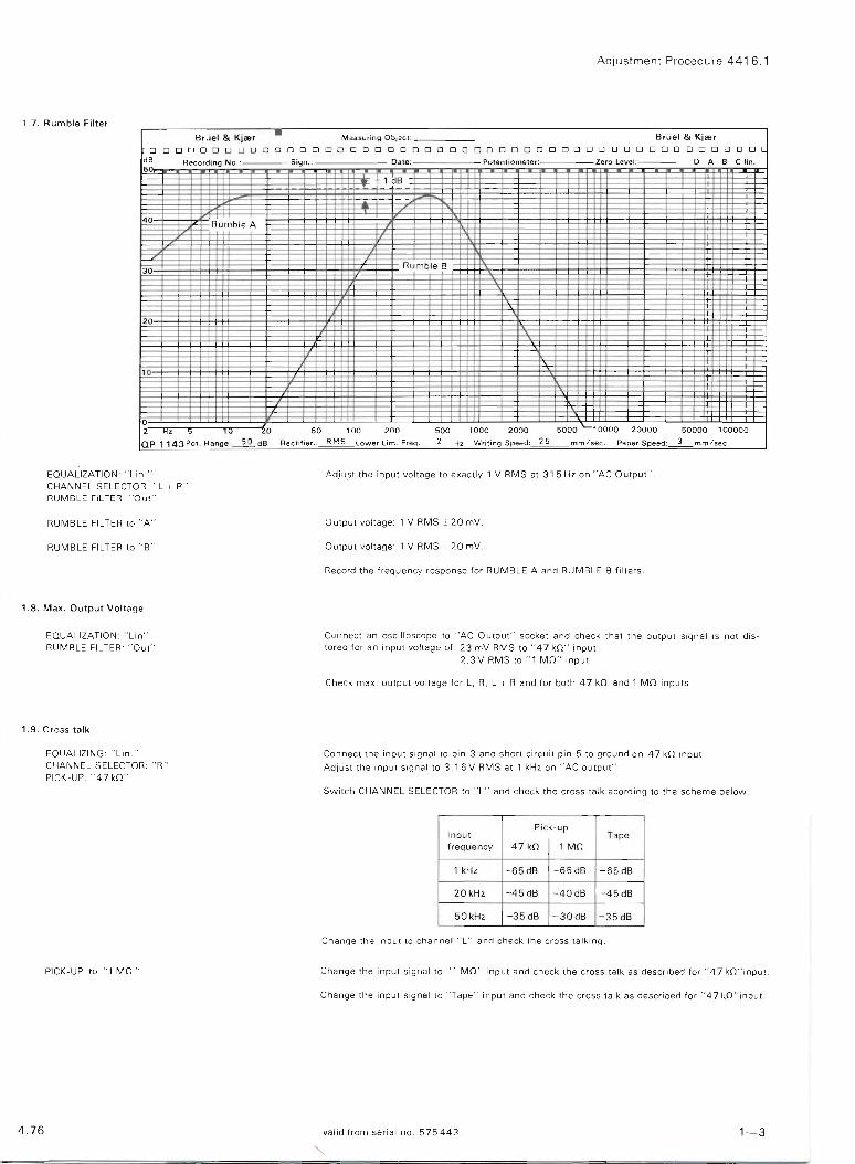
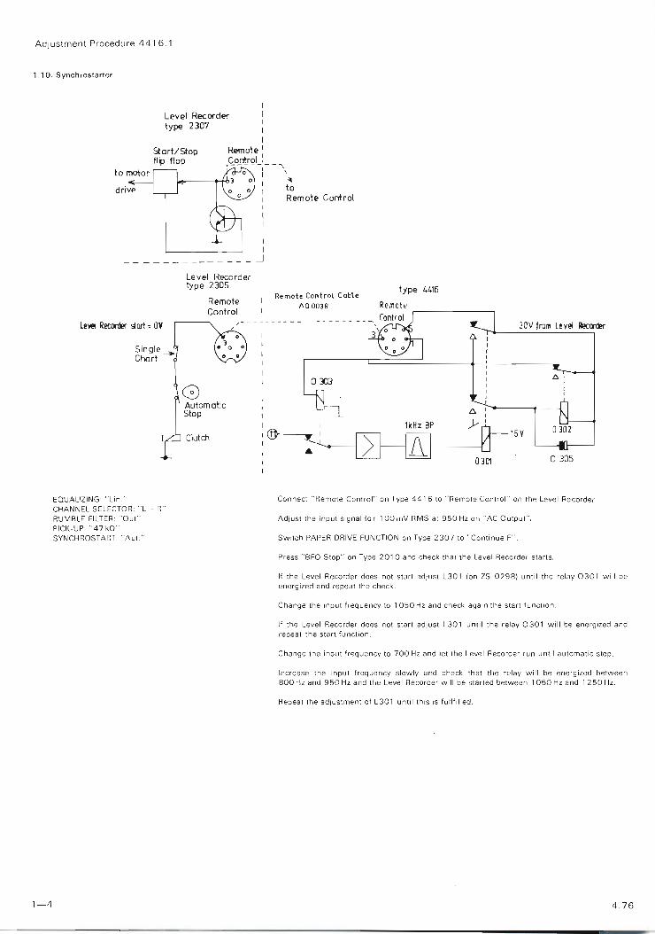
I
---- --
---------- - ------
BR UEL I Adjustment Procedure 4416 1 Noerum shy
1 10 Synchrosta rt er
Level Recorder type 2307 I
I I
StortStop Remote I
flip-flop Control ~ shyI o I
~----~
I
I I I I I
-~
Level Recorder type 2305
Remote Controi
I
~ to Remote Control
type 4416 Remot Control Cable
AQ 0039
Letllt Rero-def gart = av 30V fro l~y~ flectTilr
Single __ Chart
om G Automotic Stop
030215 VClutch
C 3ClS
EQUALlZING lin Connect Remote Contro i on Type 4416 to Remote Cont rol on the Leve l Re corder
CHA NNEL SELECTOR L + R RUMBLE FILTER Out Adjust the input signal for 100 mV RMS at 950 Hz on AC Output
PICK-UP 47 kO SYNCHROSTART Au SWllch PAPER DRIVE FUNCTION on Type 2307 to Continue F r-shy
l e
~ Press BFO Stop on Type 2010 and check that the Level Recorder starts
If the Level Recorder does not start ad just L301 (on ZS 0298) until th e relay 0301 w ill be energiled and repeat the check
Change the input frequency to 1050 Hl and check again the start function
If the Level Recorder does not start adjust L301 until the relay 0301 wi ll be energized and I repeat the stan function
Change the input frequency to 700 Hl and let the Level Recorder run unlil automatic stop
Increase the input frequency slow ly and check thaI the re lay wi ll be energiled between 800 Hl and 950 Hz and the Level Recorder will be starled between 1050 Hz and 1250 Hz
Repeat the adjustment of L301 until this is fullfilled
-eJshyR3u
1-4 4 76 176
BRUEL amp KJA R Nlterum - Denmark Circuit and Layout Diagrams ZS 0298
with Parts List Remote Controi
Remote Controi IN 41 43
Ol OJ
INC l411
Q]02
+ 15V HI e JD S
560kn JQk() AJ02 AJ 03
f------v ~ ]J ilF 4 h O
~~ AiI--4--H Ih o AJOS
I GNO 0---------------~--------1_----------~----~------~~--------L---~~ i
II
~ ~
0302 303 0301 V301302-BC107B1 J
o o 40 01o
6 o 0-~ SO 02 s S 60 03
6 6110111 ~ICw
80 o
CIRCUIT COMPONENT TYPE STOCK DIAGRAM REF REF
r--- -- ------o ()) 0 1 e 301 Polyeste r 33 nF 400 V es 0058
l () e 302 10 nF 250 V es 0403I a+o1f-1l~- II) I c 303 Polystyren e 01 JlF 63 V eT 1543
I be 1 R ~I I 1-1 11)1 e 304 Polyester 01 JlF 250 V es 0402
e 305-307 Electrolyti c 2 2JlF 63V CE 0401I ur I gtlt I l I
and L 301 Resonance Coil 250 mH LB 0196I I I I
I o 301 Relay A 2415-12V oe 0042I
een Plasti c Cover for above relay se 0014 r
o 302303 Relay RH - 24 V oe 0037I I I a 301-304 Silicon lN4148 75 V175 mA av 0216I I I
R 3 01 Carbon 1 4 W 5 4 7 kO RB 3470I I R 302 560 kO RB 5560
I R 303 10 kO RB 4100
I I R 304305 47 kO RB 4470 LO_ ~_o__~- ~rV1-irQ ~ J R 306 33 O RB 1330
R 307 1 3W 10 50 O
R 308 1 4 W 5 18 kO RB 4180
----1 f- -----fL-shye Jxx a Jx x V 301302 Silicon NPN Bel07 VB 0032
ZS 0298 Printed Circuit Board XC1292
476 176 4416 from serial no 575443
-----
BROEL amp KJAR Nrerum - Denmark Layout Diagram with Parts List ZT 0294
AmplifierPower Supply
-__--~l- - - - - - - -- =~ 32 I
I
~~~~~~~~~~~==~~middot I ~4l~~7IIIMtcnt
-cr R
-1~ C
~Q
00 v
I I I I L ________ J
viewed from the bottom side
CIRCUIT COMPONENT TYPE STOCK CIRCUIT COMPONENT TYPE STOCK DIAGRAM REF DIAGRAM REF REF REF
C 1 Ceramic 1 nF 400 V CK 3101 C 27 Polys tyrene 20 nF 63 V CT 1125
C 2 Tantalum 150pF 63V CF 0048 C 28 75nF 63V CT 1523
C 3 Polystyrene 30 nF 63 V CT 1519 C 29 Polyester 0 1 p F 250 V CS 0402
C 4 27nF 63V CT 1518 C 30 Ceramic 30 pF 400 V CK 0105
C 5 CeramlC 82pF 400V CK 0820 C 3132 Polystyrene 100 nF 63 V CT 1543
C 67 Tantalum 150pFI 63 V CF 0048 C 33 Ceramic 30 pF 400 V CK0105
C 89 15pF 20V CF 0010 C 34 Polycarbonate 022pF 63 V CS 0801
C 10 Ceramic 39 pF 400 V CK 0390 C 35 Polyester 47 nF250 V CS 0401
C 11 1 nF 400 V CK 3101 C 36 10 nF250 V CS 0403
C 12 Tantalum 150 pF 63 V CF 0048 C 37 Polystyrene 3nF63V CT 1157
C 13 Polystyrene 30 nF 63V CT 1519 C 38-41 Polyester 01 pF1250 V CS 0402
C 14 27 nF 63V CT 1518 C 42 Tantalum 47pF63V CF 0023
C 15 Ceramic 82 pF 400 V CK 0820 C 4344 Polyester 01 pF1250 V CS 0402
C 1617 Tantalum 150pF 63V CF 0048 C 45 Tantalum 47pF63V CF 0023
C 1819 15 p F 20 V CF 0010 C 4647 Polyester 01 pF1250 V CS 0402
C 20 Ceramic 39 pF 400 V CK 0390 C 4849 Ceramic 33 pF400 V CK 0330
C 21 22 Polyester 01 pF 250 V CS 0402 C 5556 82 pF400 V CK 0820
C 23 Ceramic 82pF 400V CK 0820 C 57 Polyester 022pF1 00 V CS 0339
C 24 30 pF 400 V CK0105 C 58 Ceramic 1 pF400 V CK 0100
C 25 Tantalum 2 2 p F 35 V CF 0022 C 59 10 pF 400 V CK 1100
C 26 Polycarbonate 0 l p F 100 V CS 0381 ZT 0294 C 60 Polyester 0 22pF 100V CS 0339
1 76 4416 from serial no 575443
BR UEL 8 ZT 0294 Layout Diagram with Parts List Nrerum - [
CIRCUIT COMPONENT TYPE STOCK CIRCUIT
DIAGRAM REF DIAGRAM
REF REF
C 61 Ce ramic 1 pF 400 V CK0100 R 50
C 62 10 pF 400 V CK 1100 R 51
C 63 64 Polyester O 11lF 250 V CS 0402 R 52
C 65 Ceramic 30 pF 400 V CK0105 R 53
C 6869 Electro lytic 100llFI 40V CE 0443 R 54 55
C 70 4701lF 40V CE 0417 R 56
C 71-73 Tantalum 151lFI 20V CF 0010 R 57
C 74-77 Ceramic 47 nF 30V CK 4470 R 58
C 78 Electrolytic 221lF 40 V CE 0428 R 59
R 60
R 61
P 1 Cermet 22 kO PG 3221 R 62
R 63-65
R 6667
Q 1-20 Silicon 1N4148 75 V175 mA QV 0216 R 69
Q 28-30 1N4004 400 V l A QV 0237 R 70
R 71
R 72-75
R 1 Metal 1 4W 1 61 9 kO RF 4619 R 76
R 2 Carbon 5 100 O RB 2100 R 81-87
R 3 Metal 1 2 kO RF 3200 R 90
R 4 Carbon 5 47 kO RB 4470 R 91 92
R 5 Metal 1 332 kO RF 3332 R 95 96
R 6 976 kO RF 3976 R 97
R 7 115 kO RF 5115 R 98
R 8 127 kO RF 4127 R 99100
R 9 Carbon 5 10 kO RB 4100 R 101
R 10 Metal 1 475 kO RF 3475 R 102
R 1112 475 kO RF 4475 R 103
R 13 Carbon 5 47 kO RB 4470 R 10405
R 14 Metal 1 619 kO RF 4619
R 15 Carbon 5 100 O RB 2100
R 16 Metal 1 2kO RF 3200 V
R 17 Carbon 5 47 kO RB 4470 V 2-7
R 18 Metal 1 332 kO RF 3332 V 8
R 19 9 76 kO RF 3976 V 9-13
R 20 115 kO RF 5115 V 14- 20
R 2 1 127 kO RF 4127 V 2122
R 22 Carbon 5 10 kO RB 4100 V 23 middot 25
R 23 Metal 1 475 kO RF 3475 V 26
R 24 25 475 kO RF 4475 V 27
R 26 Carbon 5 47 kO RB 4470 V 28
R 2728 Metal 1 499 kO RF 4499 V 29
R 29 1 249 kO RF 4249 V 30
R 30 Carbon 5 22 kO RB 4220 V 31
R 31 330 kO RB 5330 V 32-34
R 32 lOkO RB 4100 V 35
R 33 100 kO RB 5100 V 36
R 34 15 kO RB 4150 V 37
R 35-39 100 kO RB 5100 V 38
R 40 39 kO RB 4390
R 41 15 kO RB 4150
R 42 39 kO RB 4390
R 43 15 kO RB 4150
R 44 39 kO RB 4390
R 45 15 kO RB 4150
R 46 39 kO RB 4390
R 47 15 kO RB 4150
R 48 22 kO RB 4220
R 49 15 kO RB 4150
COMPONENT TYPE STOCK REF
Metal 1 4W 1 82 5 kO RF 4825
Carbon 5 15 kO RB 4150
Metal 1 82 5 kO AF 4825
Carbon 5 15 kO RB 4150
39 kO RB 4390
Metal 1 453 kO RF 4453
174 kO RF4174
562 kO RF 3562
Carbon 5 27 kO RB 4270
Metal 1 11 kO RF 4110
383 kO RF 3383
Carbon 5 12 kO RB 4120
100 kO RB 5100
4 7 kO RB 3470
68 kO RB 4680
47 kO RB 4470
10 kO RB 4100
1 kO RB 3100
100 O RB 2100
1 kO RB 3100
390 O RB 2390
1 kO RB 3100
Metal 1 499 kO RF 5499
316 kO RF 5316
Carbon 5 330 kO RB 5330 CIRCUIT Metal 1 499 kO RF 5499 DIAGRAM
316 kO RF 5316 REF Carbon 5 330 kO RB 5330
C 201 220 kO RB 5220
C 202 150 O RB 2150
C 203
C 204
C 205 2 x Op Amp 739 VE 0079
C 206 Op Amp 301 VE 0044
C 207 Silicon PNP BCl77 VB 0071
C 208 FET N NF510 VB 1021 C 209 Sili con PNP BCI77 VB 0071 C 210 Op Amp 301 VE 0044 C 211 FET N NF510 VB 1021 C 212 4 2 Input NANO 7400 VO 0002 C 213-215 S-R Flip-Flop 74279 VD 0073
2 4 Input NAND 7420 VD 0007
6 x INV 7416 VD 0051
4 x 2 Input NANO 7400 VD 0002
S-R Flip-Flop 74279 VD 0073
Op Amp 301 VE 0044
plusmn 15 V Regulator 4195 VE 0068
Silicon PNP 40406 VB 0053
NPN 40407 VB 0054
5 V Regulator 78M05 VE 0069
Printed C cuit Board XC 1293
Heatsink OT 0036
8 pin-Socket for dual-in-line JJ 0804
14 pin-Socket for dual-in-line JJ 1408
l 6 pin Socket for circuit board JJ 1624
176 1 76 2
BROEL amp KJAR Noorum - Denmark Layout Diagram with Parts List ZT 0 295
Input Filter
~R2 bullbull
---C2
Viewed from the top side
CIRCU IT DIAGRAM REF
COMPONENT TYPE STOCK REF
CIRCUIT DIAGRAM REF
COMPONENT TYPE STOCK REF
C 20 1
C 202
C 203
C 204
C 205
C 206
r 207
C 208
C 209
C 210
C 2 1
C 212
C 213-215
Pol ys tyrene
Ceramic
Polystyrene
Ceramic
Pol ystyr ene
Cera mic
PolYSlyrene
Ceramic
16 nF 500 V
33 pF400 V
150 pF 400 V
11 nF 63 V
130pF 100V
150pF 400V
16nF 500 V
33 pF400V
150 pF 400 V
11 nF 63 V
130 pF 1 00 V
150 pF 400 V
47 nF 30 V
CT 1103
CK 1330
CK 21 51
CT 1551
CT 1138
CK 2152
CT 1103
CK 1330
CK 2151
CT 1551
CT 1138
CK 2151
CK 4470
R
R
R
R
R
R
R
R
R
R
R
R
R
R
201
202
203
204
205
206
207
208
209
210
211
212
213
214
Metal
Carbon
M eta l
Carbon
Metal
1 4W 1
5
1
5
1
475 kO
22 1 kO
499 kO
4 7 kO
953 O
953 kO
475 O
47 5 kO
221 kO
4 99 kO
47 kO
953 O
953 kO
475 O
RF 4475
RF32 2 1
RF 3499
RB 3470
RF 2953
RF 3953
RF 2475
RF 4475
RF 3221
RF 3499
R8 3470
RF 2953
RF 3953
RF 2475
Push Button Se lector OJ 0056 V 201-204 ap Amp 301 VE 0044
Printed Circuit 8 0ard XC 1294
ZT 0295
4416 from se rial no 575443 176
BRUEL amp KJAR Nlterum - Denmark Circuit Diagram with Parts List 44162
DA 0048
Q 21 middot 27
R 77-80
R 8889
LED RL209
Carbon 14W 5 390 O
390 O
Printed Circuit Board Pnted Ccuit Board with componenlS
16-pole Flexible InterconneclOr
BNC Socket
7pin DIN Socket
Banana Sockel
Mains Socket
SlandmiddotOff
Mains Vollage Seleclor
Fuse slow 220 V
Fuse slow 110 V
Mains Transformer
QV 4001
RB 2390
RB 2390
XC 1295
OZ 0011
AR 1010
JJ 0121
JJ 0709
JT 6204
OA 0037
XL 0163
JS 0001
VF 0012
VF 0026
TN0103
~ ~e
GV 0673
Mains SWitch
Cover for above sWitch
Pi ck up Selector
5-pin DIN Socket
Circuit Board with components
Remote Controi
Amplifier Power Supply
Inpul Filter
NN 0014
DD 0088
NN 0040
JJ 0501
ZS 0098
ZT 0294
ZT 0295
1 76 valid from serial no 575443 2-1
47kO
1000 R15
Pick-up
IF
58 116kO
RS)
0221 F 2)(4g~kO
Ag R96 LIt V32
JJOU1
~+15V
OIIF
---EOlp J ~-)5V
I
SI
Right
JJOkO
11102
V26-30 SN 7400 V29- SN 7416
2731- SN 74279 V28-SN 7420 VI-)JAn9
Dv
q
g
~O bull
316~C1
RIor
V 2-7 2122 3 2-3 4 201- 204 LM 301
- I i1 +v In ll + _ ltti Dur middot0 middot- ar bull Balan CI
I
I ~ [
I I
I
I 150pF
I I cztl I
J)( 4 1 II m I JshyI l R211
I C214 C215I I 0
_150IL _______
V35-4195 15V V37-NPN 40407 V9-1323-25 V38-78M05 5V NF510
mmiddotrtv GNO I (+ ISV
Campg l -2 8alanu -V~-ISV
Top v itgtw Baltam vi ~w
Amplifiers Stereo Output
zlS0lF_--~~____-INY_IHVshy------tH C6 el
Lft
- I I
l+R
C13
I Chopper lS
F ])0 0I I I
I I ChOP
Generator
I I
I
$15 R i h t
~ -SV
+ISV
~F ~
J ~ lOOnF
~ TC41 -~ffi
I
+s +ltVO-~+--_-l OZOOll IkO
71
il l --1
~ OZ 0011
+sv kOi r- I A rgt------t-- ---- - --shyri
l
Ii +sv I Ral
lN4148 IIIn 019 R74 Ii
I 4JpfI i I+sv 1gt0TC4 I Out I ~--~~ r L_j
1k0 I R75
Rumble Filter Seleetor
Vz7 R
+
sv
Rumbe Filters
7SnF
-IVo----rshyJl00 nF
4i3~O
J- o-l nkO
59 110 12kO
38 Rumble A
52 Rumble B
10DkO
AS
Chop
lN414B W41U
011 QIO
IH41 4 8
r-T--~I-~+Smiddot
Rumble Filter Selec tor
+1iV 0----- -------shy SuF
HOD
-1 5 Yo----+--~---~~--~ OJA 220V
O2AIIOV
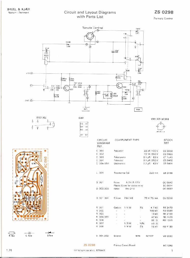
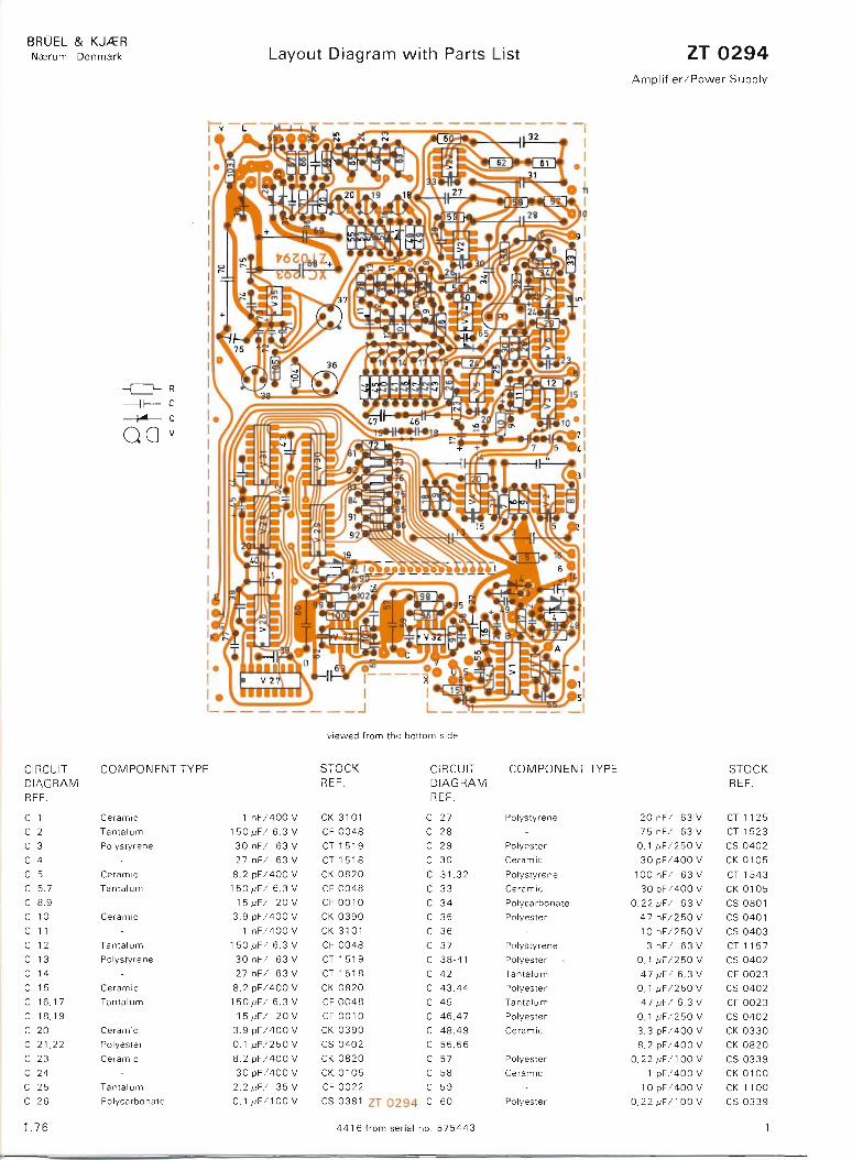
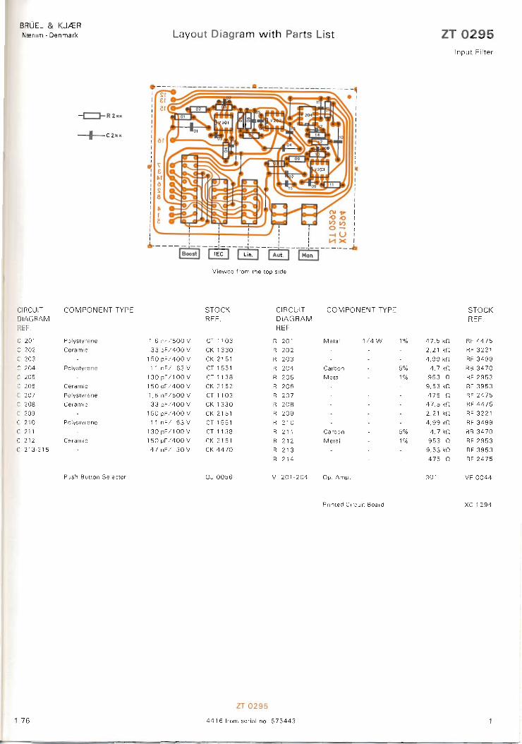
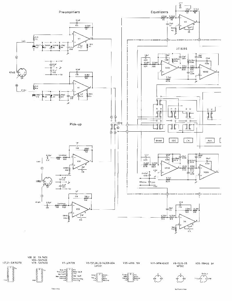

Rumbe Filters
7SnF
-IVo----rshyJl00 nF
4i3~O
J- o-l nkO
59 110 12kO
38 Rumble A
52 Rumble B
10DkO
AS
Chop
lN414B W41U
011 QIO
IH41 4 8
r-T--~I-~+Smiddot
Rumble Filter Selec tor
+1iV 0----- -------shy SuF
HOD
-1 5 Yo----+--~---~~--~ OJA 220V
O2AIIOV


![· 2013. 4. 18. · Schedule for Consider'"tion of :'Dpies ;'!emor:mduu 76-,77 (sent 8/17/76) He,.,.] Topics l1effiorandu,,-, 76-74 (sent 8/17/76) Annual ~~eport liemorandum 76-73](https://img.pdfslide.us/doc/110x75/5ff9df1700ff9b2be61957de/2013-4-18-schedule-for-considertion-of-dpies-emormduu-76-77-sent.jpg)


![Title 76 RCW - Washingtonleg.wa.gov/CodeReviser/RCWArchive/Documents/2016... · (2016 Ed.) [Title 76 RCW—page 1] Title 76 Title 76 76 FORESTS AND FOREST PRODUCTS FORESTS AND FOREST](https://img.pdfslide.us/doc/110x75/5f7a85dc890c5561e6763c0c/title-76-rcw-2016-ed-title-76-rcwapage-1-title-76-title-76-76-forests-and.jpg)