Embed Size (px)
Citation preview

Putting Electrons to Work
Doping and Semiconductor Devices

What Have We Learned About Magnetic Storage?
• Two domains magnetized in same direction is a 0• Two domains magnetized in opposite directions is
a 1• Direction of magnetization changes at start of new
bit.• Magnetic data is written by running a current
through a loop of wire near the disk• As magnetic data passes by coil of wire, changing
field induces currents according to Faraday’s Law:
dt
dBA
dt
diR B

What Have We Learned About Magnetoresistance?
• Charges traveling through magnetic field experience magnetic force (provided velocity and field are not aligned):
FB = qv x B• In a current-carrying wire, this force results in more
frequent collisions and thus an increased resistance: Magnetoresistance
• Electrons traveling through magnetized material undergo spin-dependent scattering
• When magnetic field is present in magnetic superlattice, scattering of electrons is cut dramatically, greatly decreasing resistance: Giant magnetoresistanced

What Have We Learned About Atoms?
• ENERGY IS QUANTIZED
• Electrons can absorb energy and move to a higher level; they can emit light and move to a lower level
• In hydrogen the emitted light will have energy
E = (13.6 ev)(1/nf2 – 1/ ni
2)
• The wavelength is given by = hc/E = 1240(nm eV)/E
• Energy levels of nearby atoms are slightly shifted from each other, producing bands of allowed energies
• Electrons move from the locality of one atom to the next only if an energy state is available within the same band

What have we learned about Resistance?
• In many, ohmic, materials, current is proportional to voltage:
V = iR• Resistance is proportional to the length of an
object and inversely proportional to cross-sectional area:
R = L/A• The constant of proportionality here is called the
resistivity. It is a function of material and temperature.
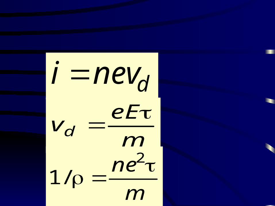
dnevi
m
eEvd
m
ne
2
/1

A Good Analogy to Remember

What Have We Learned About Solids?
• In conductors, the valence band is only partially-full, so electrons can easily move
• In semiconductors and insulators, the valence band is completely full, so electrons must gain extra energy to move– semiconductors have smaller band gap, insulators have larger band
gap
• Conductors have a partially-filled valence band– The primary effect of higher temperature on resistance is to increase
R due to more collisions at higher temperatures
• Semiconductors have a completely-filled valence band– The primary effect of temperature on resistance is due to this
requirement: the higher the temperature, the more conduction electrons

Crystal (Perfect)

Crystal (Excited)

Crystal (Excited)

Band Gap
Valence Band
Conduction Band
Band Gap Energy Eg
(Minimum Energy needed tobreak the chemical bonds)
Energy
Position

Band Gap
Valence Band
Conduction Band
Energy
Position
photon in h Eg

Band Gap
Valence Band
Conduction Band
Energy
Position
photon out

Band Gap
Valence Band
Conduction Band
Energy
Position
photon out
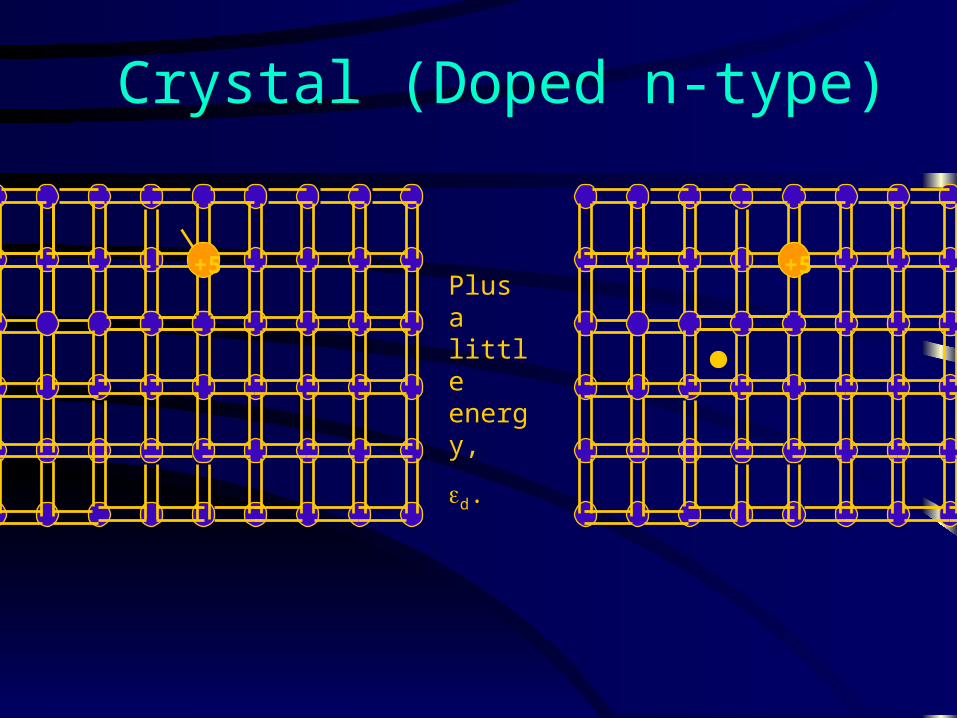
Crystal (Doped n-type)
+5 +5Plus a little energy,
d.
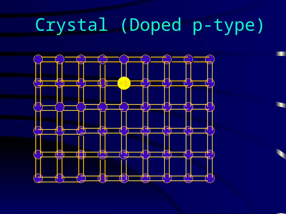
Crystal (Doped p-type)
+3

N-type semiconductors
• N-type semiconductor is doped with a material having extra valance electrons
• Result is filled energy states in the band gap just below the conduction band
• These electrons can easily gain energy to jump to the conduction band and move through the material

Crystal (Doped p-type)
+3

P-type semiconductors
• P-type semiconductor is doped with a material having fewer valance electrons
• Result is “holes”, or empty energy states in the band gap just above the valance band
• Since no single electron travels through the material, we describe the charge carrier as a positive hole moving the other way

Doped Semiconductors
Energy
n-type p-type
donor level
acceptor level
•Put them together?
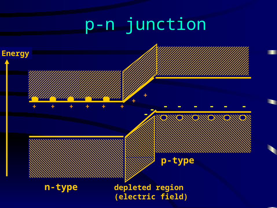
p-n junction
n-type
p-type
Energy
depleted region(electric field)
+ + + + + ++
+
--------

P-n junction• As more electrons from the n-side combine with holes from the
p-side, each additional combination adds to the potential difference across junction
• This can be envisioned as shifting the energy bands, making it harder for electrons to travel across the barrier

p-n junction
n-type
p-type
Energy
depleted region(electric field)
+ + + + + ++
+
--------
Vo

What happens if a bias is applied?

Biased junction
n-type
p-type
depleted region(electric field)
Negativebias
positivebias

Biased junction
n-type
p-type
depleted region(electric field)
Negativebias
photon out

P-n junction
• Originally both p and n sides are electrically neutral
• Electrons in n side see holes in p side and combine
Second electron needs add’l energy to get over charge barrier – can represent as rise in energy levels of p section

Forward Biasing
• Eventually, the potential difference is so large, electrons cannot travel across it without gaining energy
• Applying a forward bias decreases the potential difference so current can flow

Reverse Biasing
• Applying a reverse bias will increase the barrier rather than decreasing it, so no current flows
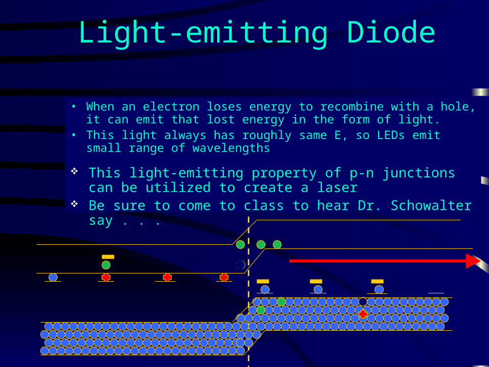
Light-emitting Diode
• When an electron loses energy to recombine with a hole, it can emit that lost energy in the form of light.
• This light always has roughly same E, so LEDs emit small range of wavelengths
This light-emitting property of p-n junctions can be utilized to create a laser
Be sure to come to class to hear Dr. Schowalter say . . .

Do Today’s Activity
• How is an incandescent light bulb different from an LED?
• What is the difference between the different colors of LED?
• Why might these differences occur?

Before the next class, . . .
• Finish Homework 16
• Do Activity 15 Evaluation by Midnight Monday
• Read Chapter 6 in Turton.


![· Web viewSolid and Semiconductor devices & Communication Devices) 1 Give the ratio of number of holes and the number of conduction electrons in an intrinsic semiconductor. [1]](https://img.pdfslide.us/doc/110x75/5b7552367f8b9a924c8d3814/-web-viewsolid-and-semiconductor-devices-communication-devices-1-give-the.jpg)