Embed Size (px)
Citation preview

Inverse Doping Profile Analysis for
Semiconductor Quality Control
Joseph K. Myers
Dissertation Abstract
PhD awarded December 12, 2009, Wichita State University
1 Preface
Today we live in an incredible computer age. Barely more than 50 years ago—an imperceptible drop in the ocean
of history’s timescale—the state-of-the-art SAGE United States national air-defense computer network [6] consisted
of 55,000 vacuum tubes powered by three megawatts of electricity and housed in facilities totaling almost two acres
in size. A tiny microprocessor today contains an electric circuit so sophisticated and complicated that it contains
40,000 times as many components, each one of which processes much larger chunks of data than a component in
the SAGE air-defense computer network. If the latest computer processors today were constructed using the same
technology as the SAGE air-defense network, they would consume more than 12 times as much power as the entire
city of New York. Yet today the same computing capability can be produced using less power than a 100-watt light
bulb!
The way that circuits so complicated can be created so small is by an incredible “printing” process.1 Instead
of printing ink onto paper, a special apparatus (Figure 1) precisely imprints an invisible electric circuit into a solid
substrate made of silicon or another semiconductor. The doping apparatus is designed to use heat and pressure to
forcibly add impurities to selected areas of the semiconductor. Even tiny concentrations of impurities can change the
electric conductivity by factors much greater than 10,000, creating the equivalent of copper wires on a microscopic
scale, each “wire“ being less than 65 nanometers thick (many times smaller than the wavelength of blue light).
The “printing” process is called “doping,” and the resulting invisible electric circuit is called the “doping profile.”
As we read on, we will see how the goal of perceiving or deducing something which is ordinarily invisible, by
mathematical methods, is called solving an inverse problem. Identification of the doping profile by mathematical
methods permits reverse engineering of the electric circuit characteristics, and thus the properties, performance, and
functionality of the semiconductor device, to achieve the goal of quality control.1In reality, the fabrication of computer chips is much more complicated than this simplified explanation.
1

Joseph K. Myers 2
2 Introduction
Both our lives and lifestyles daily depend on a host of invisible semiconductor devices, whose functionality or failure
often means life or death. If for some reason the doping compounds fail to be imprinted properly, one is faced with the
failure of a semiconductor device—nothing less than an absolute nightmare—and the necessity of improved quality
control is unbelievably emphasized. As an example, graphics giant NVIDIA lost $200 million recently because of one
set of defective chipsets, and there were several articles suggesting that a temperature offset within the foundry of
as little as four degrees Celsius was responsible; as a result, NVIDIA endured a drop in stock price from $39.67 to
$5.75, as well as losing substantial market share to rival ATI. The problem could possibly have been circumvented
by advances in quality control.
One’s goal is to achieve quality control in the manufacture of semiconductor devices, i.e., the microscopic compo-
nents and subcomponents of the electric circuits embedded through “doping profile” methods on a “computer chip.”
P-N junctions are used to form multiple types of transistors—these are fundamental building blocks of an incredible
array of semiconductor devices—on which a modern world is built: health care, medical applications, computers, cell
phones, navigational systems, and the Internet.
Currently, however, only destructive techniques, like spreading resistance profiling, are easily available for quality
control purposes. There are three stepping stones towards ultimate success in implementing non-destructive, efficient
quality control methods for semiconductor manufacturing. These are to
1. Find, develop, and use the mathematical framework underlying the semiconductor quality control problem,
including a precise mathematical definition of the semiconductor doping profile as a function C specifying the
signed difference between concentrations of positive and negative charge carriers (holes and electrons).
2. Create an efficient numerical algorithm for finding as much information about C as possible from the smallest
amount of data measurements available.
3. Fine-tune the numerical algorithm to real-world manufacturing data and real-time manufacturing environments,
enabling one to realize the final goal of producing extremely reliable semiconductor devices.
The first two goals are largely accomplished within the dissertation, with a great deal of help from results available
in the mathematical literature, especially the topics of conformal mapping and identification of coefficients in some
semilinear elliptic boundary value problems.
In Step 2, we consider the suggested numerical algorithm to be one of the most significant contributions in the
dissertation towards the final goal of quality control in the setting of industrial manufacture of semiconductor devices.
The numerical algorithm will solve many “direct” problems in order to ultimately converge to the solution of the
“inverse” problem. In the creation of the numerical algorithm, simulations are extremely important, where the speed

Joseph K. Myers 3
of the computer code can be tested and refined. One finds that execution speed can be reduced from over one minute
for a single solution of the direct problem on a 50-by-50 grid, to less than one hundredth of a second on a 100-by-100
grid, by using advanced integral equation techniques and methods of complex variables.
The result is an algorithm which can perform solution of the inverse problem from 1/3rd of a second up to 10
seconds (30 to 1,000 iterations) with four times as much accuracy, compared to an algorithm which would take from
half an hour to almost one full day and night, with four times less accuracy. Clearly these optimizations make a
difference in the suitability of the algorithm for practical use, which, to use a parallel to the previous sentence, is
just as big of a difference as the difference between night and day.
Beyond the first two steps, the final step of going beyond computer simulations to actual physical implementation
is yet to be carried out, and it will need collaboration between—at minimum—electrical engineers, semiconductor
physicists, and applied mathematicians.
3 Mathematical framework
One may look at the great timeline of history and shall find that every time scientists reached a greater understanding
of the mathematical principles governing an unknown area of electromagnetics, physics, or physical chemistry, that
almost without fail there would immediately follow great accomplishments, discoveries, and forward momentum
in the development, growth, blossoming, and maturation towards the present age of computers. Mathematics has
practical applications which far exceed the mere ability to solve esoteric puzzles—when a problem whose origin is
reality has been framed in representative mathematical terms, and when someone has then solved the mathematical
problem associated with reality, then one has the best chance, sometimes the only chance, to solve the problem that
exists, as one would say, “in the real world.” In the classical sense of Hadamard, this is the idea of a “Well-Posed
Mathematical Inverse Problem.” But the general meaning of an “Inverse Problem” is to identify a set of x-values
based on some knowledge about the functional relationship f(x) = y (“some knowledge” often corresponds to partial
differential or integral equations satisfied by x and y) and some other additional, more specific and direct, knowledge
about y. The idea of such a generalized inverse problem can be summarized by by trying to identify the criminal(s)
x by the results of their crime f(x). One cannot “see inside” of the function f , which represents the “past” or
a “forbidden region,” and so the mathematical analyst (the police detective) must deduce the identity of x (the
criminal) by more or less indirect methods. For instance, if we wish to identify the doping profile of a semiconductor
device without destroying it, then the semiconductor wafer is a “forbidden region,” containing a region of altered
electrical properties formed by addition of doping materials to the base semiconductor substrate. This “doped”
region is the unknown “x.”
The famous detective, Sherlock Holmes, in trying to explain his detective work, provides us with an excellent

Joseph K. Myers 4
Table 1: History of the inverse doping problem1947 The invention of an effective “transistor” takes place.1950 Roosbroeck develops the drift-diffusion equations for doping profiles.1953 Transistors become successful building blocks for many devices.1980 Calderon brings attention to the inverse problem for conductivity.
literary viewpoint of inverse problems:
“Most people, if you describe a train of events to them will tell you what the result would be. They can put those
events together in their minds, and argue from them that something will come to pass. There are few people, however,
who, if you told them a result, would be able to evolve from their own inner consciousness what the steps were which
led up to that result. This power is what I mean when I talk of reasoning backward, or analytically.”
— A Study in Scarlet, Sir Arthur Conan Doyle
To find the unknown “x,” we must rely on the mathematical framework that defines “x.” This is the system of
drift-diffusion equations.
Our starting point for mathematical analysis is a commonly accepted model of the semiconductor device, the
drift diffusion equations [8]. We note that this system of equations is quite similar in its properties to the equations
from Combustion Theory [1, Ch. 2]. Although the most widely accepted model for semiconductor devices, the
drift diffusion equations already represent a compromise that is made between the ideal of accurately describing the
underlying device physics, and the feasibility of computational solutions for the chosen nonlinear system of partial
differential equations.
We consider the following coupled system [10] of nonlinear partial differential equations for electrostatic potential
V , the nonnegative concentrations of free carriers of negative charge density n (electrons) and positive charge density
p (holes), which is solved in the domain Ω ⊂ Rd(d = 1, 2, 3) representing the semiconductor device, and in a time
interval [0, T ]. The dependence on time that is included in this system of equations should be emphasized.
div(εs∇V ) = q(n− p− C),
div(Dn(E, TK)∇n− µn(E, TK)n∇V ) = nt,
div(Dp(E, TK)∇p+ µp(E, TK)p∇V ) = pt,
div k(TK)∇(TK) = ρc(TK)TKt −H.
(1)
Above εs denotes the positive semiconductor permittivity coefficient (e.g., for silicon) and q the positive unit of
elementary charge—both εs and q depend on dimension; µn and µp denote the electron and hole mobility, and Dn
and Dp are the electron and hole diffusion coefficients. Observe that −∇V is the electric field with electric field
strength E = |∇V |. The function R = R(n, p, x) denotes the recombination-generation rate.
The constants ρ and c represent the specific mass density and specific heat of the material. In the thermodynamic

Joseph K. Myers 5
description, k and H denote the thermal conductivity and the locally generated heat. TK is the absolute temperature.
We assume that R is of the standard form
R = F (n, p, x)(np− n2i ), (2)
where F is a nonnegative smooth function, which holds, for example, for the frequently used Shockley-Read-Hall rate
RSRH =np− n2
i
τp(n+ ni) + τn(p+ ni). (3)
The function C = C(x) represents the doping concentration, which is produced by diffusion of different materials
into the silicon crystal (zone melting technique) and by implantation with an ion beam. When C < 0 it represents
the P region of the semiconductor and when C > 0 it represents the N region. See the literature [3, 7, 2, 8, 11] for
more details. [Note that there is a mistake in [4], which specifies on page 1,778 that C > 0 in both P and N regions.]
This system is supplemented by homogeneous Neumann boundary conditions on an insulated part ∂ΩN (open
in ∂Ω of the boundary, where zero current flow and zero electric field in the normal direction are prescribed [9]. On
the remaining part ∂ΩD (with positive (d−1)-dimensional Lebesgue measure), the following Dirichlet conditions are
imposed:
V (x, t) = VD(x, t) = U(x, t) + Vbi(x) = U(x) + UT ln(nD(x)ni
), (4)
n(x, t) = nD(x) =12
(C(x) +
√(C(x))2 + 4n2
i
), (5)
p(x, t) = pD(x) =12
(√(C(x))2 + 4n2
i − C(x)), (6)
on ∂ΩD × (0, T ), where ni is the intrinsic carrier density, UT is the (nonnegative) thermal voltage and U is the
applied potential. Moreover, the initial (time) conditions,
n(x, 0) = n0(x) ≥ 0,
p(x, 0) = p0(x) ≥ 0.(7)
have to be supplied.
4 Stationary drift-diffusion equations
The stationary drift-diffusion model is obtained from the transient model by suppressing time-dependence and omit-
ting the initial (time) conditions. We use standard assumptions about the mobilities and diffusion coefficients

Joseph K. Myers 6
(Einstein relations),
Dn = µnUT ,
Dp = µpUT ,(8)
in order to transform the system using the so-called Slotboom variables u and v defined by
n = C0δ2eV/UT u,
p = C0δ2e−V/UT v,
(9)
where
δ2 =niC0, (10)
and C0 is the doping profile scale. If we rescale all quantities to dimensionless analogues (see [8] for further details),
and if we define scaled current densities for electrons and holes,
Jn = µnδ2eV∇u,
Jp = µpδ2e−V∇v,
(11)
then we obtain the stationary system
λ24V = δ2(eV u− e−V v)− C,
div Jn = δ4Q(u, v, V, x)(uv − 1),
div Jp = −δ4Q(u, v, V, x)(uv − 1).
(12)
Above λ2 is a positive constant,
λ2 =εsUTqC0L2
, (13)
where L is a typical length scale of a semiconductor device, usually about 10−4 cm. In order to obtain a completely
non-dimensional system, we have used the scaled length x/L, and replaced the mobilities µn and µp by (UT /L)µn
and (UT /L)µp. We have also assumed εs is constant and rescaled the potential to V/UT . Also, Q is defined by the
relation F (n, p, x) = Q(u, v, V, x).
The Dirichlet boundary conditions can be written as
V = U + Vbi = U + ln(
12δ2
(C +√C2 + 4δ2)
)on ∂ΩD, (14)
Joseph K. Myers 7
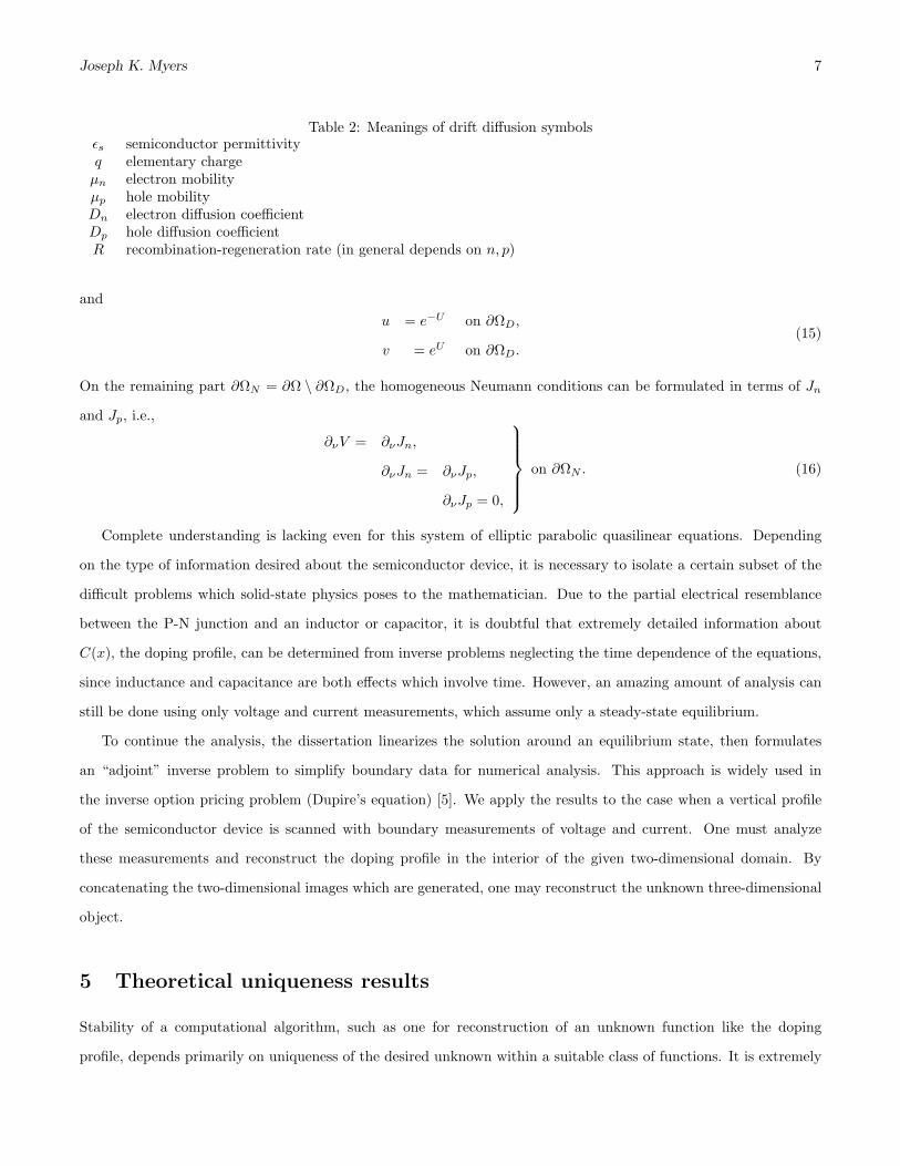
Table 2: Meanings of drift diffusion symbolsεs semiconductor permittivityq elementary chargeµn electron mobilityµp hole mobilityDn electron diffusion coefficientDp hole diffusion coefficientR recombination-regeneration rate (in general depends on n, p)
andu = e−U on ∂ΩD,
v = eU on ∂ΩD.(15)
On the remaining part ∂ΩN = ∂Ω \ ∂ΩD, the homogeneous Neumann conditions can be formulated in terms of Jn
and Jp, i.e.,
∂νV = ∂νJn,
∂νJn = ∂νJp,
∂νJp = 0,
on ∂ΩN . (16)
Complete understanding is lacking even for this system of elliptic parabolic quasilinear equations. Depending
on the type of information desired about the semiconductor device, it is necessary to isolate a certain subset of the
difficult problems which solid-state physics poses to the mathematician. Due to the partial electrical resemblance
between the P-N junction and an inductor or capacitor, it is doubtful that extremely detailed information about
C(x), the doping profile, can be determined from inverse problems neglecting the time dependence of the equations,
since inductance and capacitance are both effects which involve time. However, an amazing amount of analysis can
still be done using only voltage and current measurements, which assume only a steady-state equilibrium.
To continue the analysis, the dissertation linearizes the solution around an equilibrium state, then formulates
an “adjoint” inverse problem to simplify boundary data for numerical analysis. This approach is widely used in
the inverse option pricing problem (Dupire’s equation) [5]. We apply the results to the case when a vertical profile
of the semiconductor device is scanned with boundary measurements of voltage and current. One must analyze
these measurements and reconstruct the doping profile in the interior of the given two-dimensional domain. By
concatenating the two-dimensional images which are generated, one may reconstruct the unknown three-dimensional
object.
5 Theoretical uniqueness results
Stability of a computational algorithm, such as one for reconstruction of an unknown function like the doping
profile, depends primarily on uniqueness of the desired unknown within a suitable class of functions. It is extremely

Joseph K. Myers 8
important to determine the extent of this function class, and to use this knowledge in creation of the computational
algorithm for determining the unknown function. Hence, some of the most critical components of the dissertation
are its theoretical uniqueness results, which can be applied not only to problems in doping profile theory, but also
to similar mathematical problems, such as ion channels in inter-cellular transport. Although the uniqueness results
take up 27 pages in the original document, they can be summarized briefly in a few sentences, as follows.
Global uniqueness for a doping profile, even a discontinuous one, is proved in the case of many boundary mea-
surements (Dirichlet-to-Neumann map) by linearizing the partial differential equations around the solution with zero
boundary data, and using known results about determination of unknown coefficients by the Dirichlet-to-Neumann
map. Using a proof by contradiction, it is also proved that local uniqueness for the same class of doping profiles
holds in the case of one boundary measurement; the proof also uses results of geometric critical points and conformal
mapping index theory. Moreover, global uniqueness of a doping profile is proved in the case when Ω is the union of
sets P = x : C(x) = a and x : C(x) = b for constants a 6= b, and when P is a convex polygon.
6 Computational algorithm
We propose to identify the area, shape, and location of the obstacle D by using a three-step algorithm.
1. Generate initial data for inverse problem.
(a) Impose potential u = uD on Γ0.
(b) Measure the initial data for the inverse problem ∂νu = uN on Γ0.
2. Compute the area and radius of D.
(a) Create artificial obstacle Dr which is circular and has radius equal to r.
(b) Solve the direct problem with obstacle Dr and the same potential u(; r) = uD on Γ0 and find the resultingfunction ∂νu(; r) = uN (; r) on Γ0.
(c) Find the radius r that minimizes ‖uN (; r) − uN‖. (Here the norm ‖ · ‖ is in L∞ or another norm whichworks well in actual numerical experiments.)
(d) Fix this value of r and the area πr2 of the obstacle Dr.
3. Find the exact boundary of D by using perturbations which preserve the computed area of D.
(a) Represent D as deformations of the first approximation Dr (r is fixed, resulting from the previous step ofthe algorithm).
(b) Use a orthogonal coordinate system for the boundary of D.
∂D := γ := < x, y >:< x, y >= (r + h(s)) < sin(s), cos(s) > (17)
(c) The first approximation h(s) = 0 corresponds to Dr.
(d) For better approximations take h(s) as a linear combination of basis functions such as sines and cosines
h(s) =n∑
k=−n
(ak sin(kx) + bk cos(kx)) := a ·Bsin + b ·Bcos, (18)
where a = (a−n, a−n+1, ..., an−1, an) and b are multindexes. Write α = (a, b) as a combined multindex.

Joseph K. Myers 9
(e) Let ∂νu(;α) = uN (;α) on Γ0 be the data resulting from using the artificial domain Dα with boundaryγ(α).
(f) Minimize ‖uN (;α)− uN‖ with respect to α to obtain an n-th order approximation Dα of the domain D.
Figure 3 shows a peanut shaped domain (blue line) reconstructed (blue circles) successfully from measurements
with ±5 percent added random noise. The results shown are typical for any similar domain configuration.
7 Results
Our doping profile identification method has three primary benefits over existing methods for identifying conductivity
or doping profiles. The necessary boundary measurements are very simple. The resolution is higher than results we
have seen in the literature at the same level of noise. The type of measurements necessary are non-destructive to the
semiconductor device. It should be made clear that we have only performed computer simulations with our method,
and it has not been implemented or tested in industry.
Figures 4-13 show our method in action.
8 Industrial implementation—the step into the future
All of this mathematical and computational preparation serves only one purpose—to pose a question to researchers
the world over, “Who is going to step to the plate and work as a team to achieve the final goal of reliable, efficient,
and cost-effective quality control of semiconductor device manufacturing, based on the mathematical solution of the
inverse doping profile problem?”
Similar problems of scientific research have been posed and solved at many critical times in world history. Ex-
amples include X-ray tomography (based on the Radon Transform, none other than the mathematical solution of an
inverse problem), MRI and CAT scans, and many more fabulous, life-changing breakthroughs of science.
However, history also includes many problems that were never solved, not because it was impossible, but because
not enough people worked together, not enough were willing to build on the results of one another. In order to
achieve the goal of major improvements in semiconductor quality control, it is likely that much more work remains
than what has already been done. Is the future bright for semiconductor quality control? The answer depends on
the teamwork of many scientists—perhaps including you.

Joseph K. Myers 10
References
[1] J. Bebernes and D. Eberly. Mathematical Problems from Combustion Theory. Springer-Verlag, 1989.
[2] M. Burger, H. W. Engl, A. Leitao, and P. A. Markowich. On inverse problems for semiconductor equations.Milan J. of Mathematics, 72:273–314, 2004.
[3] Martin Burger, H. W. Engl, Peter A. Markowich, and Paola Pietra. Identification of doping profiles in semicon-ductor devices. Inverse Problems, 72:273–314, 2004.
[4] Martin Burger, Heinz W. Engl, Peter A. Markowich, and Paola Pietra. Identification of doping profiles insemiconductor devices. Inverse Problems, 17:1765–1795, 2001.
[5] Victor Isakov. Inverse Problems for Partial Differential Equations. Springer, New York, 2006.
[6] Robert W. Keyes. The long-lived transistor. American Scientist, March–April 2009.
[7] A. Leitao, P. A. Markowich, and J. P. Zubelli. On inverse doping profile problems for the stationary voltage-current map. Inverse Problems, 22:1071–1088, 2006.
[8] Peter A. Markowich, Christian A. Ringhofer, and Christian Schmeiser. Semiconductor Equations. Springer,New York, 1990.
[9] Joseph K. Myers. Theoretical results in inverse problems for size, solvability, and uniqueness in the p-n junctionand doping profile of semiconductors. Master’s thesis, Wichita State University, Wichita, 2006.
[10] W. R. Van Roosbroeck. Theory of flow of electrons and holes in germanium and other semiconductors. BellSystems Technology Journal, 29, 1950.
[11] P. Y. Yu. Fundamentals of Semiconductors: Physics and Materials Properties. Springer, 2004.

Joseph K. Myers 11
9 Appendix: Figures
Figure 1: Apparatus used for doping of semiconductor devices

Joseph K. Myers 12
Figure 2: Optimized positioning of sources for curves of integration as generated by the dissertation’s softwarepackage for Matlab

Joseph K. Myers 13
Figure 3: Good reconstruction of a peanut-shaped domain from data with 5 percent relative noise

Joseph K. Myers 14
Figure 4: The curves of integration created automatically by a subroutine we wrote as part of a Matlab package forsolving inverse conductivity problems by integral equation methods.

Joseph K. Myers 15
Figure 5: The potential surface.

Joseph K. Myers 16
Figure 6: The level curves.

Joseph K. Myers 17
Figure 7: The true data curve and noisy data points (10% relative noise) measured on the boundary of the device.

Joseph K. Myers 18
Figure 8: The solution (created only from the noisy data points and an initial guess) to the local inverse problemusing Nelder-Mead simplex functional minimization search (true domain is a solid line, the reconstruction is in opencircles, and the nearby initial guess—hence the term “local”, since a random, but nearby initial guess is generated—isshown in a dotted line). “RE” means relative error in the data, not in the doping profile. In cases when nonuniquenessholds, it is possible for the RE to be small, but for the reconstruction not to coincide with the original doping profile.

Joseph K. Myers 19
Figure 9: The solution to the local inverse problem using Newton’s Method.

Joseph K. Myers 20
Figure 10: The solution to the global inverse problem (no prior information is known or assumed; the solutio iscreated only from the noisy data points) with one degree of freedom.

Joseph K. Myers 21
Figure 11: The solution to the global inverse problem—first with 2 degrees of freedom

Joseph K. Myers 22
Figure 12: Then with 3 degrees of freedom

Joseph K. Myers 23
Figure 13: Lastly, with 4 degrees of freedom


![New E-items Added Title Author Publisher Published ... · Rare earth and transition metal doping of semiconductor materials [electronic resource] : synthesis, magnetic properties](https://img.pdfslide.us/doc/110x75/5f4d2ba8d838840a470eade3/new-e-items-added-title-author-publisher-published-rare-earth-and-transition.jpg)