Embed Size (px)
Citation preview
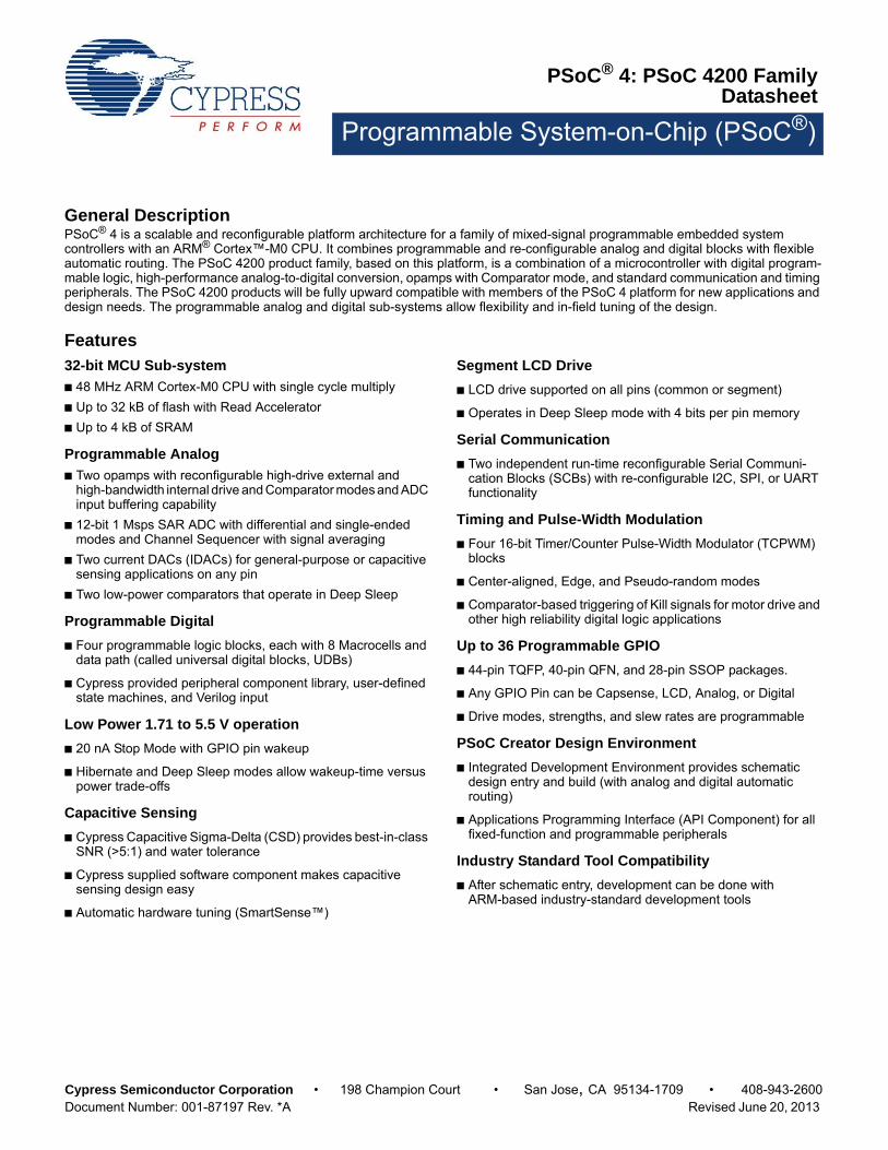
PSoC® 4: PSoC 4200 FamilyDatasheet
Programmable System-on-Chip (PSoC®)
Cypress Semiconductor Corporation • 198 Champion Court • San Jose, CA 95134-1709 • 408-943-2600Document Number: 001-87197 Rev. *A Revised June 20, 2013
General DescriptionPSoC® 4 is a scalable and reconfigurable platform architecture for a family of mixed-signal programmable embedded system controllers with an ARM® Cortex™-M0 CPU. It combines programmable and re-configurable analog and digital blocks with flexible automatic routing. The PSoC 4200 product family, based on this platform, is a combination of a microcontroller with digital program-mable logic, high-performance analog-to-digital conversion, opamps with Comparator mode, and standard communication and timing peripherals. The PSoC 4200 products will be fully upward compatible with members of the PSoC 4 platform for new applications and design needs. The programmable analog and digital sub-systems allow flexibility and in-field tuning of the design.
Features32-bit MCU Sub-system 48 MHz ARM Cortex-M0 CPU with single cycle multiply Up to 32 kB of flash with Read Accelerator Up to 4 kB of SRAM
Programmable Analog Two opamps with reconfigurable high-drive external and
high-bandwidth internal drive and Comparator modes and ADC input buffering capability
12-bit 1 Msps SAR ADC with differential and single-ended modes and Channel Sequencer with signal averaging
Two current DACs (IDACs) for general-purpose or capacitive sensing applications on any pin
Two low-power comparators that operate in Deep Sleep
Programmable Digital Four programmable logic blocks, each with 8 Macrocells and
data path (called universal digital blocks, UDBs)
Cypress provided peripheral component library, user-defined state machines, and Verilog input
Low Power 1.71 to 5.5 V operation 20 nA Stop Mode with GPIO pin wakeup
Hibernate and Deep Sleep modes allow wakeup-time versus power trade-offs
Capacitive Sensing Cypress Capacitive Sigma-Delta (CSD) provides best-in-class
SNR (>5:1) and water tolerance
Cypress supplied software component makes capacitive sensing design easy
Automatic hardware tuning (SmartSense™)
Segment LCD Drive LCD drive supported on all pins (common or segment)
Operates in Deep Sleep mode with 4 bits per pin memory
Serial Communication Two independent run-time reconfigurable Serial Communi-
cation Blocks (SCBs) with re-configurable I2C, SPI, or UART functionality
Timing and Pulse-Width Modulation Four 16-bit Timer/Counter Pulse-Width Modulator (TCPWM)
blocks
Center-aligned, Edge, and Pseudo-random modes
Comparator-based triggering of Kill signals for motor drive and other high reliability digital logic applications
Up to 36 Programmable GPIO 44-pin TQFP, 40-pin QFN, and 28-pin SSOP packages.
Any GPIO Pin can be Capsense, LCD, Analog, or Digital
Drive modes, strengths, and slew rates are programmable
PSoC Creator Design Environment Integrated Development Environment provides schematic
design entry and build (with analog and digital automatic routing)
Applications Programming Interface (API Component) for all fixed-function and programmable peripherals
Industry Standard Tool Compatibility After schematic entry, development can be done with
ARM-based industry-standard development tools
PSoC® 4: PSoC 4200 FamilyDatasheet
Document Number: 001-87197 Rev. *A Page 2 of 37
ContentsBlock Diagram .................................................................... 3Functional Definition.......................................................... 4
CPU and Memory Subsystem ....................................... 4System Resources ........................................................4Analog Blocks................................................................ 5Programmable Digital ....................................................6Fixed Function Digital ....................................................7GPIO ............................................................................. 7Special Function Peripherals......................................... 8
Pinouts ................................................................................ 9Power................................................................................. 12
Unregulated External Supply....................................... 12Regulated External Supply.......................................... 12
Development Support .......................................................13Documentation ............................................................ 13Online ..........................................................................13Tools............................................................................ 13
Electrical Specifications .................................................. 14Absolute Maximum Ratings ........................................ 14
Device Level Specifications............................................ 14Analog Peripherals .......................................................... 18Digital Peripherals .......................................................... 22Memory .......................................................................... 25System Resources ......................................................... 25
Ordering Information............................................................ 29Part Numbering Conventions ......................................... 30
Packaging............................................................................. 31Acronyms............................................................................. 34Document Conventions ...................................................... 36
Units of Measure ............................................................ 36Sales, Solutions, and Legal Information ........................... 37
Worldwide Sales and Design Support ............................ 37Products ......................................................................... 37PSoC® Solutions ........................................................... 37Cypress Developer Community...................................... 37Technical Support .......................................................... 37
PSoC® 4: PSoC 4200 FamilyDatasheet
Document Number: 001-87197 Rev. *A Page 3 of 37
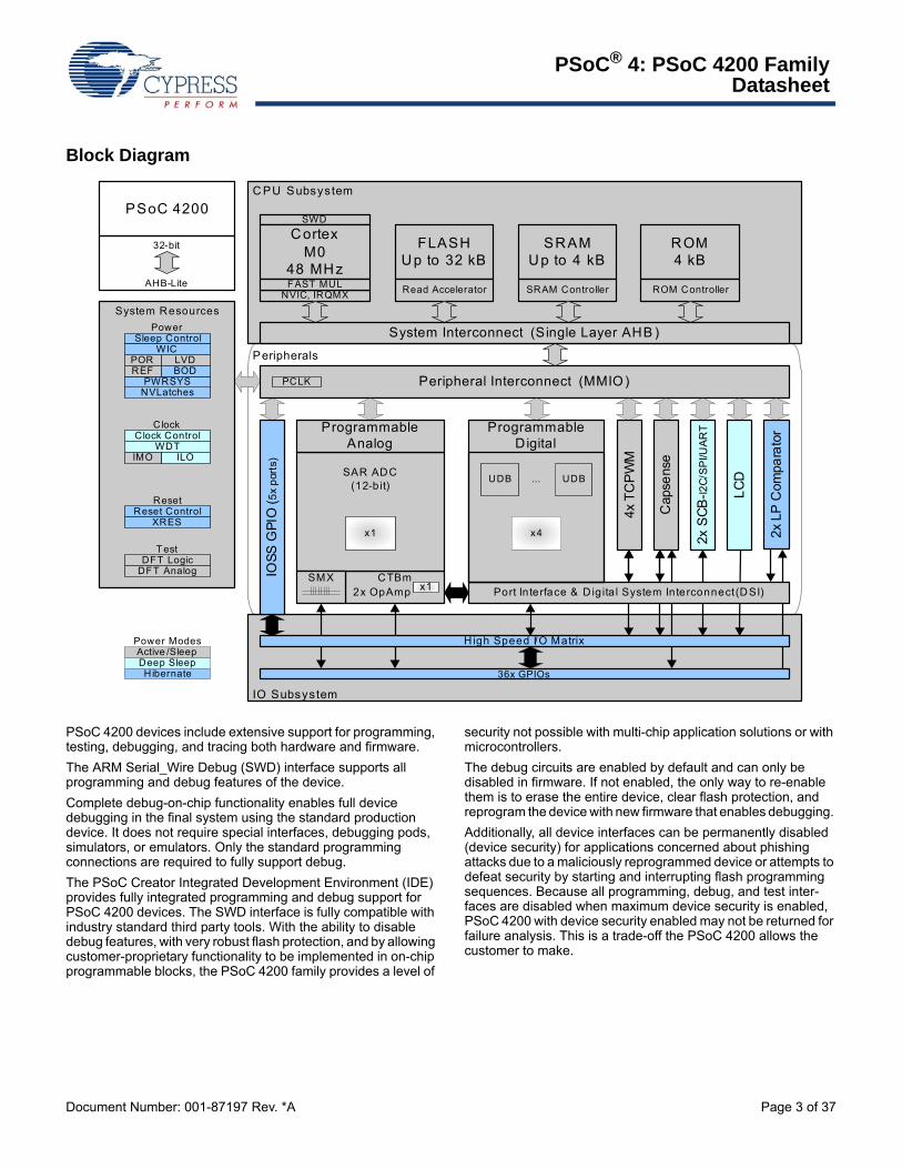
Block Diagram
PSoC 4200 devices include extensive support for programming, testing, debugging, and tracing both hardware and firmware.The ARM Serial_Wire Debug (SWD) interface supports all programming and debug features of the device.Complete debug-on-chip functionality enables full device debugging in the final system using the standard production device. It does not require special interfaces, debugging pods, simulators, or emulators. Only the standard programming connections are required to fully support debug.The PSoC Creator Integrated Development Environment (IDE) provides fully integrated programming and debug support for PSoC 4200 devices. The SWD interface is fully compatible with industry standard third party tools. With the ability to disable debug features, with very robust flash protection, and by allowing customer-proprietary functionality to be implemented in on-chip programmable blocks, the PSoC 4200 family provides a level of
security not possible with multi-chip application solutions or with microcontrollers.The debug circuits are enabled by default and can only be disabled in firmware. If not enabled, the only way to re-enable them is to erase the entire device, clear flash protection, and reprogram the device with new firmware that enables debugging. Additionally, all device interfaces can be permanently disabled (device security) for applications concerned about phishing attacks due to a maliciously reprogrammed device or attempts to defeat security by starting and interrupting flash programming sequences. Because all programming, debug, and test inter-faces are disabled when maximum device security is enabled, PSoC 4200 with device security enabled may not be returned for failure analysis. This is a trade-off the PSoC 4200 allows the customer to make.
PSoC 4200
32-bit
AHB-Lite
C PU Subsystem
SRAMUp to 4 kB
SRAM Controller
R OM4 kB
ROM Controller
FLASHUp to 32 kB
Read Accelerator
Deep SleepHibernate
Active /Sleep
SWD
NVIC, IRQMX
CortexM0
48 MHzFAST MUL
System Interconnect (Single Layer AHB )
IO Subsystem
36x GPIOs
IOSS
GPI
O (5
x po
rts)
Peripherals
System ResourcesPower
Clock
WDTILO
Reset
Clock Control
DFT LogicTest
IMO
DFT Analog
Sleep Control
PWRSYSREFPOR LVD
NVLatches
BOD
WIC
Reset ControlXRES
Peripheral Interconnect (MMIO)PCLK
4x T
CPW
M
LCD
2x S
CB-I2
C/SP
I/UAR
T
2x L
P C
ompa
rato
r
Cap
sens
e
Port In terface & D ig ita l System Interconnect (DSI)
ProgrammableDigital
x4
UDB...UDB
Power Modes
CTBmSMX
SAR ADC(12-bit)
x1
ProgrammableAnalog
x12x OpAmp
High Speed I/O Matrix
PSoC® 4: PSoC 4200 FamilyDatasheet
Document Number: 001-87197 Rev. *A Page 4 of 37
Functional DefinitionCPU and Memory Subsystem
CPUThe Cortex-M0 CPU in the PSoC 4200 is part of the 32-bit MCU subsystem, which is optimized for low power operation with extensive clock gating. It mostly uses 16-bit instructions and executes a subset of the Thumb-2 instruction set. This enables fully compatible binary upward migration of the code to higher performance processors such as the Cortex-M3 and M4, thus enabling upward compatibility. The Cypress implementation includes a hardware multiplier that provides a 32-bit result in one cycle. It includes a nested vectored interrupt controller (NVIC) block with 32 interrupt inputs and also includes a Wakeup Interrupt Controller (WIC), which can wake the processor up from Deep Sleep mode allowing power to be switched off to the main processor when the chip is in Deep Sleep mode. The Cortex-M0 CPU provides a Non-Maskable Interrupt input (NMI), which is made available to the user when it is not in use for system functions requested by the user.The CPU also includes a debug interface, the Serial Wire Debug (SWD) interface, which is a 2-wire form of JTAG; the debug configuration used for PSoC 4200 has four break-point (address) comparators and two watchpoint (data) comparators.
FlashThe PSoC 4200 has a flash module with a flash accelerator tightly coupled to the CPU to improve average access times from the flash block. The flash block is designed to deliver 1 wait-state (WS) access time at 48 MHz and with 0 WS access time at 24 MHz. The flash accelerator delivers 85% of single-cycle SRAM access performance on average. Part of the flash module can be used to emulate EEPROM operation if required.
SRAMSRAM memory is retained during Hibernate.
SROMA supervisory ROM that contains boot and configuration routines is provided.
System Resources
Power SystemThe power system is described in detail in the section Power on page 12. It provides assurance that voltage levels are as required for each respective mode and either delay mode entry (on power-on reset (POR), for example) until voltage levels are as required for proper function or generate resets (Brown-Out Detect (BOD)) or interrupts (Low Voltage Detect (LVD)). The PSoC 4200 operates with a single external supply over the range of 1.71 to 5.5 V and has five different power modes, transitions between which are managed by the power system. The PSoC 4200 provides Sleep, Deep Sleep, Hibernate, and Stop low-power modes.
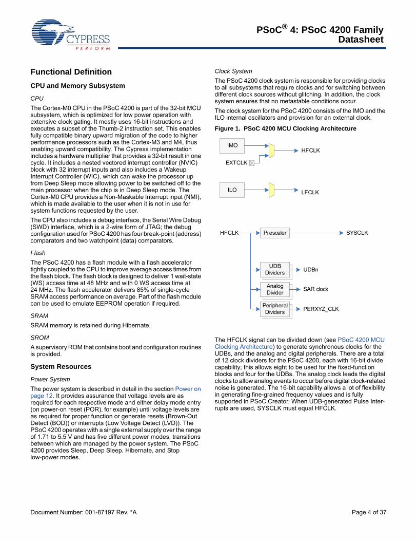
Clock SystemThe PSoC 4200 clock system is responsible for providing clocks to all subsystems that require clocks and for switching between different clock sources without glitching. In addition, the clock system ensures that no metastable conditions occur. The clock system for the PSoC 4200 consists of the IMO and the ILO internal oscillators and provision for an external clock.
Figure 1. PSoC 4200 MCU Clocking Architecture
The HFCLK signal can be divided down (see PSoC 4200 MCU Clocking Architecture) to generate synchronous clocks for the UDBs, and the analog and digital peripherals. There are a total of 12 clock dividers for the PSoC 4200, each with 16-bit divide capability; this allows eight to be used for the fixed-function blocks and four for the UDBs. The analog clock leads the digital clocks to allow analog events to occur before digital clock-related noise is generated. The 16-bit capability allows a lot of flexibility in generating fine-grained frequency values and is fully supported in PSoC Creator. When UDB-generated Pulse Inter-rupts are used, SYSCLK must equal HFCLK.
UDB Dividers
Analog Divider
Peripheral Dividers
SYSCLKPrescalerHFCLK
UDBn
SAR clock
PERXYZ_CLK
IMO
ILO
HFCLK
LFCLK
EXTCLK
PSoC® 4: PSoC 4200 FamilyDatasheet
Document Number: 001-87197 Rev. *A Page 5 of 37
IMO Clock SourceThe IMO is the primary source of internal clocking in the PSoC 4200. It is trimmed during testing to achieve the specified accuracy. Trim values are stored in nonvolatile latches (NVL). Additional trim settings from flash can be used to compensate for changes. The IMO default frequency is 24 MHz and it can be adjusted between 3 to 48 MHz in steps of 1 MHz. IMO Tolerance with Cypress-provided calibration settings is ±2%.
ILO Clock SourceThe ILO is a very low power oscillator, which is primarily used to generate clocks for peripheral operation in Deep Sleep mode. ILO-driven counters can be calibrated to the IMO to improve accuracy. Cypress provides a software component, which does the calibration.
Watchdog TimerA watchdog timer is implemented in the clock block running from the ILO; this allows watchdog operation during Deep Sleep and generates a watchdog reset if not serviced before the timeout occurs. The watchdog reset is recorded in the Reset Cause register.
ResetThe PSoC 4200 can be reset from a variety of sources including a software reset. Reset events are asynchronous and guarantee reversion to a known state. The reset cause is recorded in a register, which is sticky through reset and allows software to determine the cause of the Reset. An XRES pin is reserved for external reset to avoid complications with configuration and multiple pin functions during power-on or reconfiguration.
Voltage ReferenceThe PSoC 4200 reference system generates all internally required references. A 1% voltage reference spec is provided for the 12-bit ADC. To allow better signal to noise ratios (SNR) and better absolute accuracy, it is possible to bypass the internal reference using a GPIO pin or to use an external reference for the SAR.
Analog Blocks
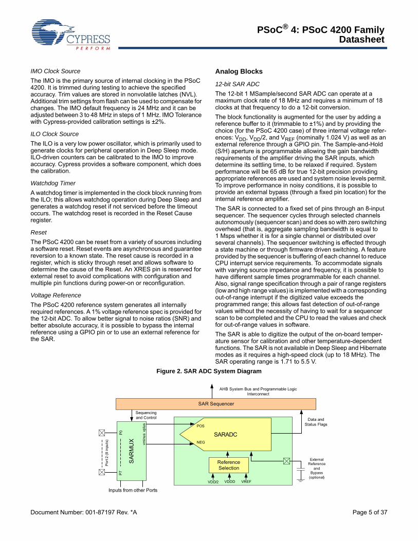
12-bit SAR ADCThe 12-bit 1 MSample/second SAR ADC can operate at a maximum clock rate of 18 MHz and requires a minimum of 18 clocks at that frequency to do a 12-bit conversion. The block functionality is augmented for the user by adding a reference buffer to it (trimmable to ±1%) and by providing the choice (for the PSoC 4200 case) of three internal voltage refer-ences: VDD, VDD/2, and VREF (nominally 1.024 V) as well as an external reference through a GPIO pin. The Sample-and-Hold (S/H) aperture is programmable allowing the gain bandwidth requirements of the amplifier driving the SAR inputs, which determine its settling time, to be relaxed if required. System performance will be 65 dB for true 12-bit precision providing appropriate references are used and system noise levels permit. To improve performance in noisy conditions, it is possible to provide an external bypass (through a fixed pin location) for the internal reference amplifier. The SAR is connected to a fixed set of pins through an 8-input sequencer. The sequencer cycles through selected channels autonomously (sequencer scan) and does so with zero switching overhead (that is, aggregate sampling bandwidth is equal to 1 Msps whether it is for a single channel or distributed over several channels). The sequencer switching is effected through a state machine or through firmware driven switching. A feature provided by the sequencer is buffering of each channel to reduce CPU interrupt service requirements. To accommodate signals with varying source impedance and frequency, it is possible to have different sample times programmable for each channel. Also, signal range specification through a pair of range registers (low and high range values) is implemented with a corresponding out-of-range interrupt if the digitized value exceeds the programmed range; this allows fast detection of out-of-range values without the necessity of having to wait for a sequencer scan to be completed and the CPU to read the values and check for out-of-range values in software.The SAR is able to digitize the output of the on-board temper-ature sensor for calibration and other temperature-dependent functions. The SAR is not available in Deep Sleep and Hibernate modes as it requires a high-speed clock (up to 18 MHz). The SAR operating range is 1.71 to 5.5 V.
Figure 2. SAR ADC System Diagram
SAR
MU
X
Por
t 2 (8
inpu
ts)
vplu
svm
inus
P0
P7
Data and Status Flags
Reference Selection
External Reference
and Bypass
(optional)
POS
NEG
SAR Sequencer
SARADC
Inputs from other Ports
VDD/2 VDDD VREF
AHB System Bus and Programmable Logic Interconnect
Sequencing and Control
PSoC® 4: PSoC 4200 FamilyDatasheet
Document Number: 001-87197 Rev. *A Page 6 of 37
Two Opamps (CTBm Block)The PSoC 4200 has two opamps with Comparator modes which allow most common analog functions to be performed on-chip eliminating external components; PGAs, Voltage Buffers, Filters, Trans-Impedance Amplifiers, and other functions can be realized with external passives saving power, cost, and space. The on-chip opamps are designed with enough bandwidth to drive the Sample-and-Hold circuit of the ADC without requiring external buffering.
Temperature SensorThe PSoC 4200 has one on-chip temperature sensor This consists of a diode, which is biased by a current source that can be disabled to save power. The temperature sensor is connected to the ADC, which digitizes the reading and produces a temper-ature value using Cypress supplied software that includes calibration and linearization.
Low-power ComparatorsThe PSoC 4200 has a pair of low-power comparators, which can also operate in the Deep Sleep and Hibernate modes. This allows the analog system blocks to be disabled while retaining the ability to monitor external voltage levels during low-power modes. The comparator outputs are normally synchronized to avoid metastability unless operating in an asynchronous power mode (Hibernate) where the system wake-up circuit is activated by a comparator switch event.
Programmable Digital
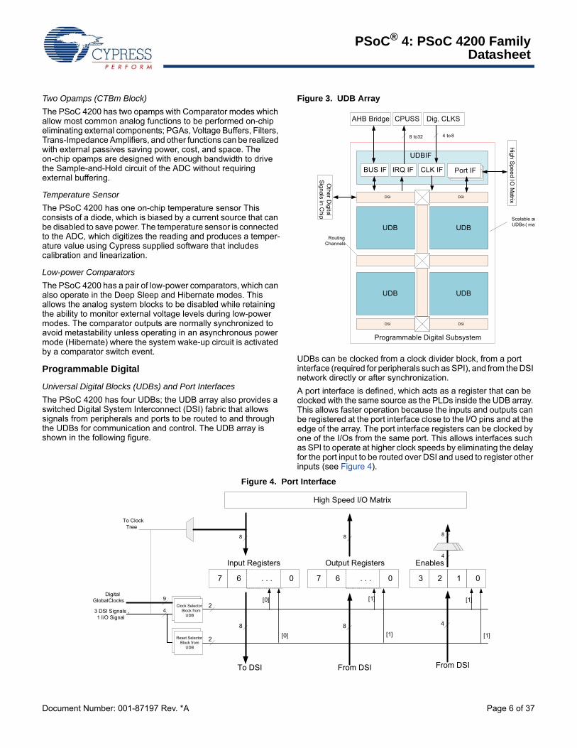
Universal Digital Blocks (UDBs) and Port InterfacesThe PSoC 4200 has four UDBs; the UDB array also provides a switched Digital System Interconnect (DSI) fabric that allows signals from peripherals and ports to be routed to and through the UDBs for communication and control. The UDB array is shown in the following figure.
Figure 3. UDB Array
UDBs can be clocked from a clock divider block, from a port interface (required for peripherals such as SPI), and from the DSI network directly or after synchronization. A port interface is defined, which acts as a register that can be clocked with the same source as the PLDs inside the UDB array. This allows faster operation because the inputs and outputs can be registered at the port interface close to the I/O pins and at the edge of the array. The port interface registers can be clocked by one of the I/Os from the same port. This allows interfaces such as SPI to operate at higher clock speeds by eliminating the delay for the port input to be routed over DSI and used to register other inputs (see Figure 4).
Figure 4. Port Interface
Programmable Digital Subsystem
UDBIF
UDB UDB
UDB UDB
DSI DSI
DSI DSI
BUS IF IRQ IF CLK IF Port IFPort IFPort IF
High Speed
IO M
atrix
CPUSSAHB Bridge Dig. CLKS
4 to 88 to 32
Scalable arUDBs ( max
RoutingChannels
Other Digital
Signals in
Chip
Clock Selector Block from
UDB
9Digital
GlobalClocks
3 DSI Signals , 1 I/O Signal
4
Reset Selector Block from
UDB
2
2
Input Registers Output Registers
To DSI
8
From DSI
8
8 8
Enables
8
From DSI
4
4
7 6 . . . 0 7 6 . . . 0 3 2 1 0
High Speed I/O Matrix
To Clock Tree
[0]
[0]
[1]
[1]
[1]
[1]
PSoC® 4: PSoC 4200 FamilyDatasheet
Document Number: 001-87197 Rev. *A Page 7 of 37
The UDBs can generate interrupts (one UDB at a time) to the interrupt controller. The UDBs retain the ability to connect to any pin on the chip through the DSI.
Fixed Function Digital
Timer/Counter/PWM BlockThe Timer/Counter/PWM block consists of four 16-bit counters with user-programmable period length. There is a Capture register to record the count value at the time of an event (which may be an I/O event), a period register which is used to either stop or auto-reload the counter when its count is equal to the period register, and compare registers to generate compare value signals which are used as PWM duty cycle outputs. The block also provides true and complementary outputs with programmable offset between them to allow use as deadband programmable complementary PWM outputs. It also has a Kill input to force outputs to a predetermined state; for example, this is used in motor drive systems when an overcurrent state is indicated and the PWMs driving the FETs need to be shut off immediately with no time for software intervention.
Serial Communication Blocks (SCB)The PSoC 4200 has two SCBs, which can each implement an I2C, UART, or SPI interface. I2C Mode: The hardware I2C block implements a full multi-master and slave interface (it is capable of multimaster arbitration). This block is capable of operating at speeds of up to 1 Mbps (Fast Mode Plus) and has flexible buffering options to reduce interrupt overhead and latency for the CPU. It also supports EzI2C that creates a mailbox address range in the memory of the PSoC 4200 and effectively reduces I2C commu-nication to reading from and writing to an array in memory. In addition, the block supports an 8-deep FIFO for receive and transmit which, by increasing the time given for the CPU to read data, greatly reduces the need for clock stretching caused by the CPU not having read data on time. The FIFO mode is available in all channels and is very useful in the absence of DMA. The I2C peripheral is compatible with the I2C Standard-mode, Fast-mode, and Fast-mode Plus devices as defined in the NXP I2C-bus specification and user manual (UM10204). The I2C bus I/O is implemented with GPIO in open-drain modes.The PSoC 4200 is not completely compliant with the I2C spec in the following respects:
GPIO cells are not overvoltage tolerant and, therefore, cannot be hot-swapped or powered up independently of the rest of the I2C system.
Fast-mode Plus has an IOL specification of 20 mA at a VOL of 0.4 V. The GPIO cells can sink a maximum of 8 mA IOL with a VOL maximum of 0.6 V.
Fast-mode and Fast-mode Plus specify minimum Fall times, which are not met with the GPIO cell; Slow strong mode can help meet this spec depending on the Bus Load.
When the SCB is an I2C Master, it interposes an IDLE state between NACK and Repeated Start; the I2C spec defines Bus free as following a Stop condition so other Active Masters do not intervene but a Master that has just become activated may start an Arbitration cycle.
When the SCB is in I2C Slave mode, and Address Match on External Clock is enabled (EC_AM = 1) along with operation in the internally clocked mode (EC_OP = 0), then its I2C address must be even.
UART Mode: This is a full-feature UART operating at up to 1 Mbps. It supports automotive single-wire interface (LIN), infrared interface (IrDA), and SmartCard (ISO7816) protocols, all of which are minor variants of the basic UART protocol. In addition, it supports the 9-bit multiprocessor mode that allows addressing of peripherals connected over common RX and TX lines. Common UART functions such as parity error, break detect, and frame error are supported. An 8-deep FIFO allows much greater CPU service latencies to be tolerated. Note that hardware handshaking is not supported. This is not commonly used and can be implemented with a UDB-based UART in the system, if required.SPI Mode: The SPI mode supports full Motorola SPI, TI SSP (essentially adds a start pulse used to synchronize SPI Codecs), and National Microwire (half-duplex form of SPI). The SPI block can use the FIFO and also supports an EzSPI mode in which data interchange is reduced to reading and writing an array in memory.
GPIO The PSoC 4200 has 36 GPIOs. The GPIO block implements the following:
Eight drive strength modes: Analog input mode (input and output buffers disabled) Input only Weak pull-up with strong pull-down Strong pull-up with weak pull-down Open drain with strong pull-down Open drain with strong pull-up Strong pull-up with strong pull-down Weak pull-up with weak pull-down
Input threshold select (CMOS or LVTTL).
Individual control of input and output buffer enabling/disabling in addition to the drive strength modes.
Hold mode for latching previous state (used for retaining I/O state in Deep Sleep mode and Hibernate modes).
Selectable slew rates for dV/dt related noise control to improve EMI.
PSoC® 4: PSoC 4200 FamilyDatasheet
Document Number: 001-87197 Rev. *A Page 8 of 37
The pins are organized in logical entities called ports, which are 8-bit in width. During power-on and reset, the blocks are forced to the disable state so as not to crowbar any inputs and/or cause excess turn-on current. A multiplexing network known as a high-speed I/O matrix is used to multiplex between various signals that may connect to an I/O pin. Pin locations for fixed-function peripherals are also fixed to reduce internal multi-plexing complexity (these signals do not go through the DSI network). DSI signals are not affected by this and any pin may be routed to any UDB through the DSI network.Data output and pin state registers store, respectively, the values to be driven on the pins and the states of the pins themselves.Every I/O pin can generate an interrupt if so enabled and each I/O port has an interrupt request (IRQ) and interrupt service routine (ISR) vector associated with it (5 for PSoC 4200 since it has 4.5 ports).
Special Function Peripherals
LCD Segment DriveThe PSoC 4200 has an LCD controller which can drive up to four commons and up to 32 segments. It uses full digital methods to drive the LCD segments requiring no generation of internal LCD voltages. The two methods used are referred to as digital corre-lation and PWM. Digital correlation pertains to modulating the frequency and levels of the common and segment signals to generate the highest RMS voltage across a segment to light it up or to keep the RMS signal zero. This method is good for STN displays but may result in reduced contrast with TN (cheaper) displays.
PWM pertains to driving the panel with PWM signals to effec-tively use the capacitance of the panel to provide the integration of the modulated pulse-width to generate the desired LCD voltage. This method results in higher power consumption but can result in better results when driving TN displays. LCD operation is supported during Deep Sleep refreshing a small display buffer (4 bits; 1 32-bit register per port).
CapSenseCapSense is supported on all pins in the PSoC 4200 through a CapSense Sigma-Delta (CSD) block that can be connected to any pin through an analog mux bus that any GPIO pin can be connected to via an Analog switch. CapSense function can thus be provided on any pin or group of pins in a system under software control. A component is provided for the CapSense block to make it easy for the user.Shield voltage can be driven on another Mux Bus to provide water tolerance capability. Water tolerance is provided by driving the shield electrode in phase with the sense electrode to keep the shield capacitance from attenuating the sensed input.The CapSense block has two IDACs which can be used for general purposes if CapSense is not being used.(both IDACs are available in that case) or if CapSense is used without water tolerance (one IDAC is available).
PSoC® 4: PSoC 4200 FamilyDatasheet
Document Number: 001-87197 Rev. *A Page 9 of 37
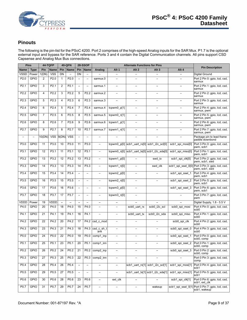
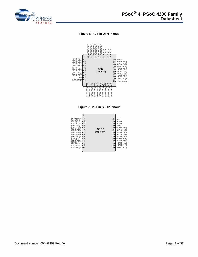
PinoutsThe following is the pin-list for the PSoC 4200. Port 2 comprises of the high-speed Analog inputs for the SAR Mux. P1.7 is the optional external input and bypass for the SAR reference. Ports 3 and 4 contain the Digital Communication channels. All pins support CSD Capsense and Analog Mux Bus connections.
Pins 44-TQFP 40-QFN 28-SSOP Alternate Functions for PinsPin Description
Name Type Pin Name Pin Name Pin Name Analog Alt 1 Alt 2 Alt 3 Alt 4VSSD Power 1(DN) VSS DN – DN – – – – – – Digital GroundP2.0 GPIO 2 P2.0 1 P2.0 – – sarmux.0 – – – – Port 2 Pin 0: gpio, lcd, csd,
sarmuxP2.1 GPIO 3 P2.1 2 P2.1 – – sarmux.1 – – – – Port 2 Pin 1: gpio, lcd, csd,
sarmuxP2.2 GPIO 4 P2.2 3 P2.2 5 P2.2 sarmux.2 – – – – Port 2 Pin 2: gpio, lcd, csd,
sarmuxP2.3 GPIO 5 P2.3 4 P2.3 6 P2.3 sarmux.3 – – – – Port 2 Pin 3: gpio, lcd, csd,
sarmuxP2.4 GPIO 6 P2.4 5 P2.4 7 P2.4 sarmux.4 tcpwm0_p[1] – – – Port 2 Pin 4: gpio, lcd, csd,
sarmux, pwmP2.5 GPIO 7 P2.5 6 P2.5 8 P2.5 sarmux.5 tcpwm0_n[1] – – – Port 2 Pin 5: gpio, lcd, csd,
sarmux, pwmP2.6 GPIO 8 P2.6 7 P2.6 9 P2.6 sarmux.6 tcpwm1_p[1] – – – Port 2 Pin 6: gpio, lcd, csd,
sarmux, pwmP2.7 GPIO 9 P2.7 8 P2.7 10 P2.7 sarmux.7 tcpwm1_n[1] – – – Port 2 Pin 7: gpio, lcd, csd,
sarmux, pwm– – 10(DN) VSS 9(DN) VSS – – – – – – – Package pin to lead frame
paddle downbondP3.0 GPIO 11 P3.0 10 P3.0 11 P3.0 – tcpwm0_p[0] scb1_uart_rx[0] scb1_i2c_scl[0] scb1_spi_mosi[0] Port 3 Pin 0: gpio, lcd, csd,
pwm, scb1P3.1 GPIO 12 P3.1 11 P3.1 12 P3.1 – tcpwm0_n[0] scb1_uart_tx[0] scb1_i2c_sda[0] scb1_spi_miso[0] Port 3 Pin 1: gpio, lcd, csd,
pwm, scb1P3.2 GPIO 13 P3.2 12 P3.2 13 P3.2 – tcpwm1_p[0] – swd_io scb1_spi_clk[0] Port 3 Pin 2: gpio, lcd, csd,
pwm, scb1, swdP3.3 GPIO 14 P3.3 13 P3.3 14 P3.3 – tcpwm1_n[0] – swd_clk scb1_spi_ssel_0[0] Port 3 Pin 3: gpio, lcd, csd,
pwm, scb1, swdP3.4 GPIO 15 P3.4 14 P3.4 – – – tcpwm2_p[0] – – scb1_spi_ssel_1 Port 3 Pin 4: gpio, lcd, csd,
pwm, scb1P3.5 GPIO 16 P3.5 15 P3.5 – – – tcpwm2_n[0] – – scb1_spi_ssel_2 Port 3 Pin 5: gpio, lcd, csd,
pwm, scb1P3.6 GPIO 17 P3.6 16 P3.6 – – – tcpwm3_p[0] – scb1_spi_ssel_3 Port 3 Pin 6: gpio, lcd, csd,
pwm, scb1P3.7 GPIO 18 P3.7 17 P3.7 – – – tcpwm3_n[0] – – Port 3 Pin 7: gpio, lcd, csd,
pwmVDDD Power 19 VDDD – – – – – – – – – Digital Supply, 1.8 - 5.5 VP4.0 GPIO 20 P4.0 18 P4.0 15 P4.0 – – scb0_uart_rx scb0_i2c_scl scb0_spi_mosi Port 4 Pin 0: gpio, lcd, csd,
scb0P4.1 GPIO 21 P4.1 19 P4.1 16 P4.1 – – scb0_uart_tx scb0_i2c_sda scb0_spi_miso Port 4 Pin 1: gpio, lcd, csd,
scb0P4.2 GPIO 22 P4.2 20 P4.2 17 P4.2 csd_c_mod – – – scb0_spi_clk Port 4 Pin 2: gpio, lcd, csd,
scb0P4.3 GPIO 23 P4.3 21 P4.3 18 P4.3 csd_c_sh_t
ank– – – scb0_spi_ssel_0 Port 4 Pin 3: gpio, lcd, csd,
scb0P0.0 GPIO 24 P0.0 22 P0.0 19 P0.0 comp1_inp – – – scb0_spi_ssel_1 Port 0 Pin 0: gpio, lcd, csd,
scb0, compP0.1 GPIO 25 P0.1 23 P0.1 20 P0.1 comp1_inn – – – scb0_spi_ssel_2 Port 0 Pin 1: gpio, lcd, csd,
scb0, compP0.2 GPIO 26 P0.2 24 P0.2 21 P0.2 comp2_inp – – – scb0_spi_ssel_3 Port 0 Pin 2: gpio, lcd, csd,
scb0, compP0.3 GPIO 27 P0.3 25 P0.3 22 P0.3 comp2_inn – – – – Port 0 Pin 3: gpio, lcd, csd,
compP0.4 GPIO 28 P0.4 26 P0.4 – – – – scb1_uart_rx[1] scb1_i2c_scl[1] scb1_spi_mosi[1] Port 0 Pin 4: gpio, lcd, csd,
scb1P0.5 GPIO 29 P0.5 27 P0.5 – – – – scb1_uart_tx[1] scb1_i2c_sda[1] scb1_spi_miso[1] Port 0 Pin 5: gpio, lcd, csd,
scb1P0.6 GPIO 30 P0.6 28 P0.6 23 P0.6 – ext_clk – – scb1_spi_clk[1] Port 0 Pin 6: gpio, lcd, csd,
scb1, ext_clkP0.7 GPIO 31 P0.7 29 P0.7 24 P0.7 – – – wakeup scb1_spi_ssel_0[1] Port 0 Pin 7: gpio, lcd, csd,
scb1, wakeup
PSoC® 4: PSoC 4200 FamilyDatasheet
Document Number: 001-87197 Rev. *A Page 10 of 37
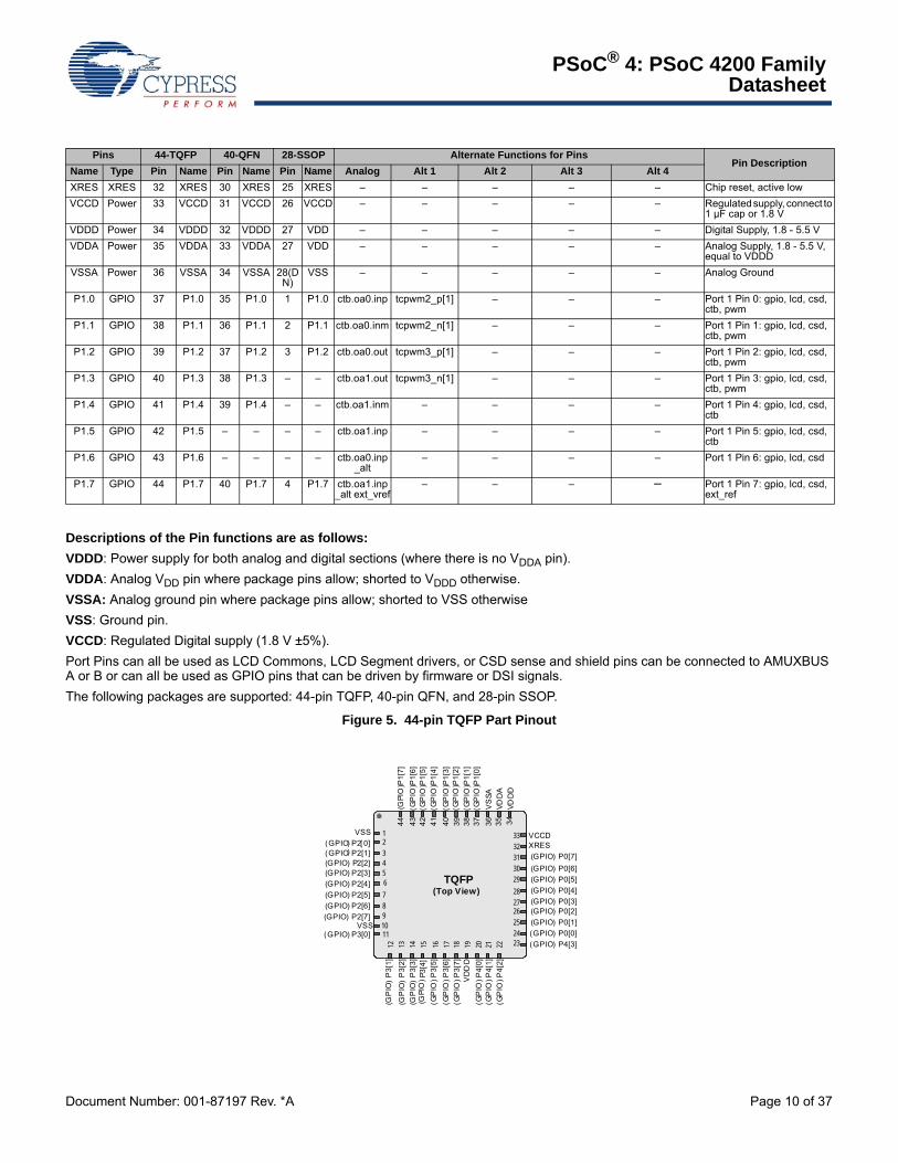
Descriptions of the Pin functions are as follows:VDDD: Power supply for both analog and digital sections (where there is no VDDA pin).VDDA: Analog VDD pin where package pins allow; shorted to VDDD otherwise.VSSA: Analog ground pin where package pins allow; shorted to VSS otherwiseVSS: Ground pin.VCCD: Regulated Digital supply (1.8 V ±5%).Port Pins can all be used as LCD Commons, LCD Segment drivers, or CSD sense and shield pins can be connected to AMUXBUS A or B or can all be used as GPIO pins that can be driven by firmware or DSI signals.The following packages are supported: 44-pin TQFP, 40-pin QFN, and 28-pin SSOP.
Figure 5. 44-pin TQFP Part Pinout
XRES XRES 32 XRES 30 XRES 25 XRES – – – – – Chip reset, active lowVCCD Power 33 VCCD 31 VCCD 26 VCCD – – – – – Regulated supply, connect to
1 µF cap or 1.8 VVDDD Power 34 VDDD 32 VDDD 27 VDD – – – – – Digital Supply, 1.8 - 5.5 VVDDA Power 35 VDDA 33 VDDA 27 VDD – – – – – Analog Supply, 1.8 - 5.5 V,
equal to VDDDVSSA Power 36 VSSA 34 VSSA 28(D
N)VSS – – – – – Analog Ground
P1.0 GPIO 37 P1.0 35 P1.0 1 P1.0 ctb.oa0.inp tcpwm2_p[1] – – – Port 1 Pin 0: gpio, lcd, csd, ctb, pwm
P1.1 GPIO 38 P1.1 36 P1.1 2 P1.1 ctb.oa0.inm tcpwm2_n[1] – – – Port 1 Pin 1: gpio, lcd, csd, ctb, pwm
P1.2 GPIO 39 P1.2 37 P1.2 3 P1.2 ctb.oa0.out tcpwm3_p[1] – – – Port 1 Pin 2: gpio, lcd, csd, ctb, pwm
P1.3 GPIO 40 P1.3 38 P1.3 – – ctb.oa1.out tcpwm3_n[1] – – – Port 1 Pin 3: gpio, lcd, csd, ctb, pwm
P1.4 GPIO 41 P1.4 39 P1.4 – – ctb.oa1.inm – – – – Port 1 Pin 4: gpio, lcd, csd, ctb
P1.5 GPIO 42 P1.5 – – – – ctb.oa1.inp – – – – Port 1 Pin 5: gpio, lcd, csd, ctb
P1.6 GPIO 43 P1.6 – – – – ctb.oa0.inp_alt
– – – – Port 1 Pin 6: gpio, lcd, csd
P1.7 GPIO 44 P1.7 40 P1.7 4 P1.7 ctb.oa1.inp_alt ext_vref
– – – – Port 1 Pin 7: gpio, lcd, csd, ext_ref
Pins 44-TQFP 40-QFN 28-SSOP Alternate Functions for PinsPin Description
Name Type Pin Name Pin Name Pin Name Analog Alt 1 Alt 2 Alt 3 Alt 4
TQFP(Top View)
VDD
D
1011
P2[1]
3332313029282726252423
36 35 34
23456789
12 13 14 15 16 17 18 19 20 21 22
VSS(GPIO) P2[ 0](GPIO) (GPIO) P2[2](GPIO) P2[3](GPIO) P2[4](GPIO) P2[5](GPIO) P2[6](GPIO) P2[7]
VSS(GPIO) P3[0]
(GP
IO)
P3[
1]
(GPI
O) P
3[4]
(GP
IO) P
3[5]
(GP
IO) P
3[6]
(GP
IO) P
3[7]
VD
DD
(GP
IO) P
4[0]
(GP
IO) P
4[1]
(GP
IO) P
4[2]
VDD
A
(GPIO) P4[3](GPIO) P0[0](GPIO) P0[1](GPIO) P0[2](GPIO) P0[3](GPIO) P0[4](GPIO) P0[5](GPIO) P0[6](GPIO) P0[7]
XRESVCCD
VS
SA(G
PIO
)P1[
0]
37383940
1
41424344
(GP
IO)P
1[1]
(G
PIO
)P1[
2]
(GP
IO)P
1[3]
(G
PIO
)P1[
4]
(GP
IO)P
1[5]
(G
PIO
)P1[
6](G
PIO
)P1[
7](G
PIO
) P
3[2]
(GP
IO)
P3[
3]
PSoC® 4: PSoC 4200 FamilyDatasheet
Document Number: 001-87197 Rev. *A Page 11 of 37
Figure 6. 40-Pin QFN Pinout
Figure 7. 28-Pin SSOP Pinout
QFN(Top View)
10
11
30292827262524232221
33 32 31
23456789
12 13 14 15 16 17
18 19 20
(GP
IO)
P3[3
]
(GPIO) P2[1]
(GPIO) P2[3](GPIO) P2[4](GPIO) P2[5](GPIO) P2[6](GPIO) P2[7]
Vss
(GPI
O) P
3[1]
(GPI
O) P
3[2]
(GP
IO)P
3[5]
(GP
IO)
P3[6
](G
PIO
) P3
[7]
(GP
IO)
P4[0
]
(GP
IO)
P4[1
](G
PIO
) P4
[2]
(GPIO) P4[3](GPIO) P0[0]
VD
DD
(GPIO) P0[1](GPIO) P0[2](GPIO) P0[3](GPIO) P0[4](GPIO) P0[5](GPIO) P0[6](GPIO) P0[7]XRES
(GP
IO)
P3[4
]
VD
DA
VS
SA34353637
1
383940
(GP
IO)P
1[0]
(GP
IO)P
1[1]
(G
PIO
)P1[
2]
(GP
IO)P
1[3]
(G
PIO
)P1[
4]
(GP
IO)P
1[7]
VC
CD
(GPIO) P3[0]
(GPIO) P2[0]
(GPIO) P2[2]
(GPIO) P0[1]
SSOP(Top View)
1011
P1[2]
28272625
23222120191817
23456789
(GPIO) P1[1](GPIO) (GPIO) P1[7](GPIO) P2[2](GPIO) P2[3](GPIO) P2[4](GPIO) P2[5](GPIO) P2[6]
(GPIO) P3[0] (GPIO) P4[3](GPIO) P0[0]
(GPIO) P0[2](GPIO) P0[3](GPIO) P0[6](GPIO) P0[7]XRES
VDDDVSS1
121314
( GPIO) P1[0]
(GPIO) P3[1](GPIO) P3[2](GPIO) P3[3]
(GPIO) P2[7 ]
(GPIO) P4[2]
VCCD
(GPIO) P4[1](GPIO) P4[0]
1615
24
PSoC® 4: PSoC 4200 FamilyDatasheet
Document Number: 001-87197 Rev. *A Page 12 of 37
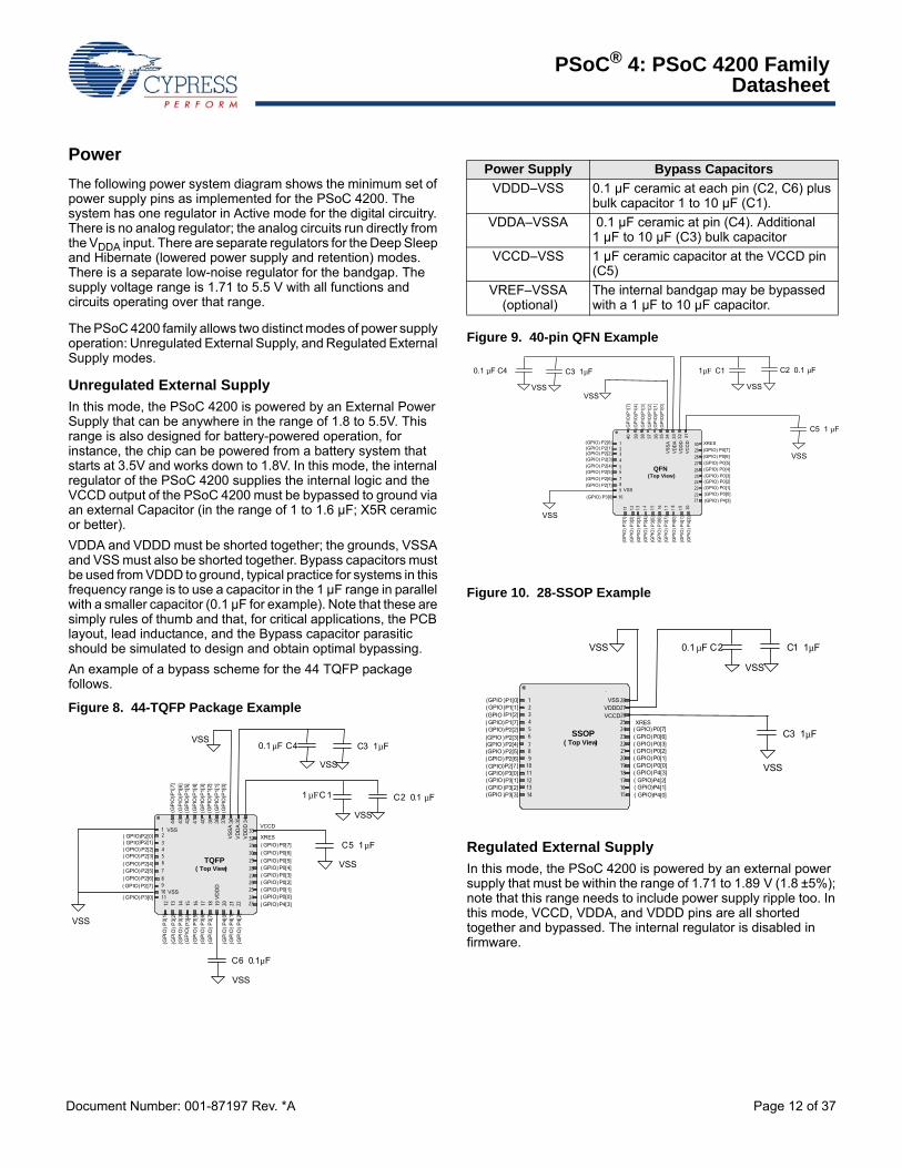
PowerThe following power system diagram shows the minimum set of power supply pins as implemented for the PSoC 4200. The system has one regulator in Active mode for the digital circuitry. There is no analog regulator; the analog circuits run directly from the VDDA input. There are separate regulators for the Deep Sleep and Hibernate (lowered power supply and retention) modes. There is a separate low-noise regulator for the bandgap. The supply voltage range is 1.71 to 5.5 V with all functions and circuits operating over that range.
The PSoC 4200 family allows two distinct modes of power supply operation: Unregulated External Supply, and Regulated External Supply modes.
Unregulated External SupplyIn this mode, the PSoC 4200 is powered by an External Power Supply that can be anywhere in the range of 1.8 to 5.5V. This range is also designed for battery-powered operation, for instance, the chip can be powered from a battery system that starts at 3.5V and works down to 1.8V. In this mode, the internal regulator of the PSoC 4200 supplies the internal logic and the VCCD output of the PSoC 4200 must be bypassed to ground via an external Capacitor (in the range of 1 to 1.6 µF; X5R ceramic or better). VDDA and VDDD must be shorted together; the grounds, VSSA and VSS must also be shorted together. Bypass capacitors must be used from VDDD to ground, typical practice for systems in this frequency range is to use a capacitor in the 1 µF range in parallel with a smaller capacitor (0.1 µF for example). Note that these are simply rules of thumb and that, for critical applications, the PCB layout, lead inductance, and the Bypass capacitor parasitic should be simulated to design and obtain optimal bypassing.An example of a bypass scheme for the 44 TQFP package follows.
Figure 8. 44-TQFP Package Example
Figure 9. 40-pin QFN Example
Figure 10. 28-SSOP Example
Regulated External SupplyIn this mode, the PSoC 4200 is powered by an external power supply that must be within the range of 1.71 to 1.89 V (1.8 ±5%); note that this range needs to include power supply ripple too. In this mode, VCCD, VDDA, and VDDD pins are all shorted together and bypassed. The internal regulator is disabled in firmware.
C2 0.1 µF
VSS
TQFP( Top View)
VDD
D
1011
P2[1]
3332313029282726252423
36 35 34
23456789
12 13 14 15 16 17 18 19 20 21 22
VSS( GPIO) P2[0]
( GPIO) ( GPIO) P2[2]( GPIO) P2[3]( GPIO) P2[4]( GPIO) P2[5]( GPIO) P2[6]( GPIO) P2[7]
VSS( GPIO) P3[0]
(GPI
O) P
3[1]
(GPI
O) P
3[4]
(GPI
O) P
3[5]
(GPI
O) P
3[6]
(GPI
O) P
3[7]
VD
DD
(GPI
O) P
4[0]
(GPI
O) P
4[1]
(GPI
O) P
4[2]
VD
DA
( GPIO) P4[3]( GPIO) P0[0]( GPIO) P0[1]( GPIO) P0[2]( GPIO) P0[3]( GPIO) P0[4]( GPIO) P0[5]( GPIO) P0[6]( GPIO) P0[7]XRES
VCCD
VSSA
(GPI
O)P
1[0]
37383940
1
41424344
(GPI
O)P
1[1]
(G
PIO
)P1[
2]
(GPI
O)P
1[3]
(G
PIO
)P1[
4]
(GPI
O)P
1[5]
(G
PIO
)P1[
6](G
PIO
)P1[
7](G
PIO
) P3[
2](G
PIO
) P3[
3]
VSS
1 µF C 1
C5 1µF
0.1 µF C4 C3 1µF
C6 0.1µF
VSS
VSS
VSS
VSS
Power Supply Bypass CapacitorsVDDD–VSS 0.1 µF ceramic at each pin (C2, C6) plus
bulk capacitor 1 to 10 µF (C1). VDDA–VSSA 0.1 µF ceramic at pin (C4). Additional
1 µF to 10 µF (C3) bulk capacitorVCCD–VSS 1 µF ceramic capacitor at the VCCD pin
(C5)VREF–VSSA
(optional)The internal bandgap may be bypassed with a 1 µF to 10 µF capacitor.
(GP
IO) P
3[3]
(GP
IO) P
4[1]
(GP
IO) P
4[2]
(GP
IO) P
3[4]
0.1 µF C4
C5 1 µF
QFN(Top View)
10
11
30292827262524232221
33 32 31
23456789
12 13 14 15 16 17 18 19 2 0
(GPIO) P2[1]
(GPIO) P2[3](GPIO) P2[4](GPIO) P2[5](GPIO) P2[6](GPIO) P2[7]
VSS
(GPI
O) P
3[1]
(GPI
O) P
3[2]
(GP
IO) P
3[5]
(GP
IO) P
3[6]
(GP
IO) P
3[7]
(GP
IO) P
4[0]
(GPIO) P4[3](GPIO) P0[0]
VDD
D
(GPIO) P0[1](GPIO) P0[2](GPIO) P0[3](GPIO) P0[4](GPIO) P0[5](GPIO) P0[6](GPIO) P0[7]XRES
VDD
AV
SSA
34353637
1
383940
(GPI
O)P
1[0]
(GPI
O)P
1[1]
(G
PIO
)P1[
2]
(GPI
O)P
1[3]
(G
PIO
)P1[
4](G
PIO
)P1[
7]
VCC
D
(GPIO) P3[0]
(GPIO) P2[0]
(GPIO) P2[2]
VSSVSS
VSS
VSS
VSS
C3 1µF 1µF C1 C2 0.1 µF
( GPIO) P3[0]
( GPIO) P0[1]
SSOP( Top View)
1011
P1[2]
28272625
23222120191817
23456789
(GPIO) P1[1](GPIO ) ( GPIO) P1[7]( GPIO) P2[2](GPIO ) P2[3](GPIO ) P2[4](GPIO) P2[5](GPIO) 2[6]
( GPIO) P4[3]( GPIO) P0[0]
( GPIO) P0[2]( GPIO) P0[3]( GPIO) P0[6]( GPIO) P0[7]XRES
VDDDVSS1
121314
(GPIO ) P1[0]
(GPIO) P3[1](GPIO) P3[2](GPIO ) P3[3]
(GPIO) P2[7]
( GPIO) P4[2]
VCCD
( GPIO) P4[1]( GPIO) P4[0]
1615
24 C3 1µF
VSS
VSS
0.1µF C2 C1 1µF VSS
P
PSoC® 4: PSoC 4200 FamilyDatasheet
Document Number: 001-87197 Rev. *A Page 13 of 37
Development SupportThe PSoC 4200 family has a rich set of documentation, devel-opment tools, and online resources to assist you during your development process. Visit www.cypress.com/go/psoc4 to find out more.
DocumentationA suite of documentation supports the PSoC 4200 family to ensure that you can find answers to your questions quickly. This section contains a list of some of the key documents.Software User Guide: A step-by-step guide for using PSoC Creator. The software user guide shows you how the PSoC Creator build process works in detail, how to use source control with PSoC Creator, and much more.Component Datasheets: The flexibility of PSoC allows the creation of new peripherals (components) long after the device has gone into production. Component data sheets provide all of the information needed to select and use a particular component, including a functional description, API documentation, example code, and AC/DC specifications.
Application Notes: PSoC application notes discuss a particular application of PSoC in depth; examples include brushless DC motor control and on-chip filtering. Application notes often include example projects in addition to the application note document.Technical Reference Manual: The Technical Reference Manual (TRM) contains all the technical detail you need to use a PSoC device, including a complete description of all PSoC registers.
OnlineIn addition to print documentation, the Cypress PSoC forums connect you with fellow PSoC users and experts in PSoC from around the world, 24 hours a day, 7 days a week.
ToolsWith industry standard cores, programming, and debugging interfaces, the PSoC 4200 family is part of a development tool ecosystem. Visit us at www.cypress.com/go/psoccreator for the latest information on the revolutionary, easy to use PSoC Creator IDE, supported third party compilers, programmers, debuggers, and development kits.
PSoC® 4: PSoC 4200 FamilyDatasheet
Document Number: 001-87197 Rev. *A Page 14 of 37
Electrical SpecificationsAbsolute Maximum Ratings
Device Level SpecificationsAll specifications are valid for -40 °C ≤ TA ≤ 85 °C and TJ ≤ 100 °C, except where noted. Specifications are valid for 1.71 V to 5.5 V, except where noted.
Note1. Usage above the absolute maximum conditions listed in Table 1 may cause permanent damage to the device. Exposure to Absolute Maximum conditions for
extended periods of time may affect device reliability. When used below Absolute Maximum conditions but above normal operating conditions, the device may not operate to specification.
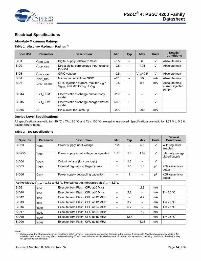
Table 1. Absolute Maximum Ratings[1]
Spec ID# Parameter Description Min Typ Max Units Details/Conditions
SID1 VDDD_ABS Digital supply relative to Vssd –0.5 – 6 V Absolute maxSID2 VCCD_ABS Direct digital core voltage input relative
to Vssd–0.5 – 1.95 V Absolute max
SID3 VGPIO_ABS GPIO voltage –0.5 – VDD+0.5 V Absolute maxSID4 IGPIO_ABS Maximum current per GPIO –25 – 25 mA Absolute maxSID5 IGPIO_injection GPIO injection current, Max for VIH >
VDDD, and Min for VIL < VSS
–0.5 – 0.5 mA Absolute max, current injected per pin
BID44 ESD_HBM Electrostatic discharge human body model
2200 – – V
BID45 ESD_CDM Electrostatic discharge charged device model
500 – – V
BID46 LU Pin current for Latch-up –200 – 200 mA
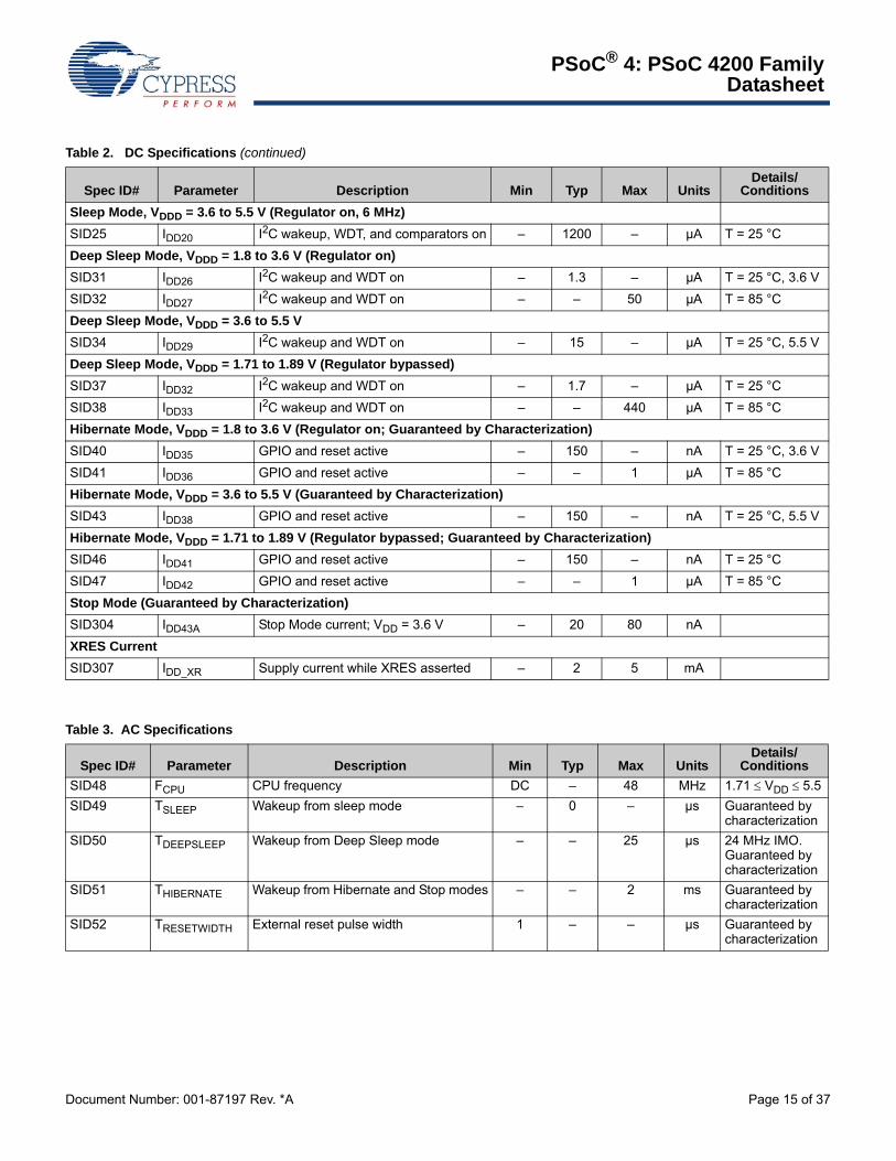
Table 2. DC Specifications
Spec ID# Parameter Description Min Typ Max UnitsDetails/
ConditionsSID53 VDDD Power supply input voltage 1.8 – 5.5 V With regulator
enabledSID255 VDDD Power supply input voltage unregulated 1.71 1.8 1.89 V Internally unreg-
ulated supplySID54 VCCD Output voltage (for core logic) – 1.8 – VSID55 CEFC External regulator voltage bypass 1 1.3 1.6 µF X5R ceramic or
betterSID56 CEXC Power supply decoupling capacitor – 1 – µF X5R ceramic or
betterActive Mode, VDDD = 1.71 to 5.5 V. Typical values measured at VDD = 3.3 V.SID9 IDD5 Execute from Flash; CPU at 6 MHz – – 2.8 mASID10 IDD6 Execute from Flash; CPU at 6 MHz – 2.2 – mA T = 25 °CSID12 IDD8 Execute from Flash; CPU at 12 MHz – – 4.2 mASID13 IDD9 Execute from Flash; CPU at 12 MHz – 3.7 – mA T = 25 °CSID16 IDD11 Execute from Flash; CPU at 24 MHz – 6.7 – mA T = 25 °CSID17 IDD12 Execute from Flash; CPU at 24 MHz – – 7.2 mASID19 IDD14 Execute from Flash; CPU at 48 MHz – 12.8 – mA T = 25 °CSID20 IDD15 Execute from Flash; CPU at 48 MHz – – 13.8 mA
PSoC® 4: PSoC 4200 FamilyDatasheet
Document Number: 001-87197 Rev. *A Page 15 of 37
Sleep Mode, VDDD = 3.6 to 5.5 V (Regulator on, 6 MHz)SID25 IDD20 I2C wakeup, WDT, and comparators on – 1200 – µA T = 25 °CDeep Sleep Mode, VDDD = 1.8 to 3.6 V (Regulator on)SID31 IDD26 I2C wakeup and WDT on – 1.3 – µA T = 25 °C, 3.6 VSID32 IDD27 I2C wakeup and WDT on – – 50 µA T = 85 °CDeep Sleep Mode, VDDD = 3.6 to 5.5 VSID34 IDD29 I2C wakeup and WDT on – 15 – µA T = 25 °C, 5.5 VDeep Sleep Mode, VDDD = 1.71 to 1.89 V (Regulator bypassed)SID37 IDD32 I2C wakeup and WDT on – 1.7 – µA T = 25 °CSID38 IDD33 I2C wakeup and WDT on – – 440 µA T = 85 °CHibernate Mode, VDDD = 1.8 to 3.6 V (Regulator on; Guaranteed by Characterization)SID40 IDD35 GPIO and reset active – 150 – nA T = 25 °C, 3.6 VSID41 IDD36 GPIO and reset active – – 1 µA T = 85 °CHibernate Mode, VDDD = 3.6 to 5.5 V (Guaranteed by Characterization)SID43 IDD38 GPIO and reset active – 150 – nA T = 25 °C, 5.5 VHibernate Mode, VDDD = 1.71 to 1.89 V (Regulator bypassed; Guaranteed by Characterization)SID46 IDD41 GPIO and reset active – 150 – nA T = 25 °CSID47 IDD42 GPIO and reset active – – 1 µA T = 85 °CStop Mode (Guaranteed by Characterization)SID304 IDD43A Stop Mode current; VDD = 3.6 V – 20 80 nAXRES CurrentSID307 IDD_XR Supply current while XRES asserted – 2 5 mA
Table 2. DC Specifications (continued)
Spec ID# Parameter Description Min Typ Max UnitsDetails/
Conditions
Table 3. AC Specifications
Spec ID# Parameter Description Min Typ Max UnitsDetails/
ConditionsSID48 FCPU CPU frequency DC – 48 MHz 1.71 ≤ VDD ≤ 5.5SID49 TSLEEP Wakeup from sleep mode – 0 – µs Guaranteed by
characterizationSID50 TDEEPSLEEP Wakeup from Deep Sleep mode – – 25 µs 24 MHz IMO.
Guaranteed by characterization
SID51 THIBERNATE Wakeup from Hibernate and Stop modes – – 2 ms Guaranteed by characterization
SID52 TRESETWIDTH External reset pulse width 1 – – µs Guaranteed by characterization
PSoC® 4: PSoC 4200 FamilyDatasheet
Document Number: 001-87197 Rev. *A Page 16 of 37
GPIO
Note2. VIH must not exceed VDDD + 0.2 V.
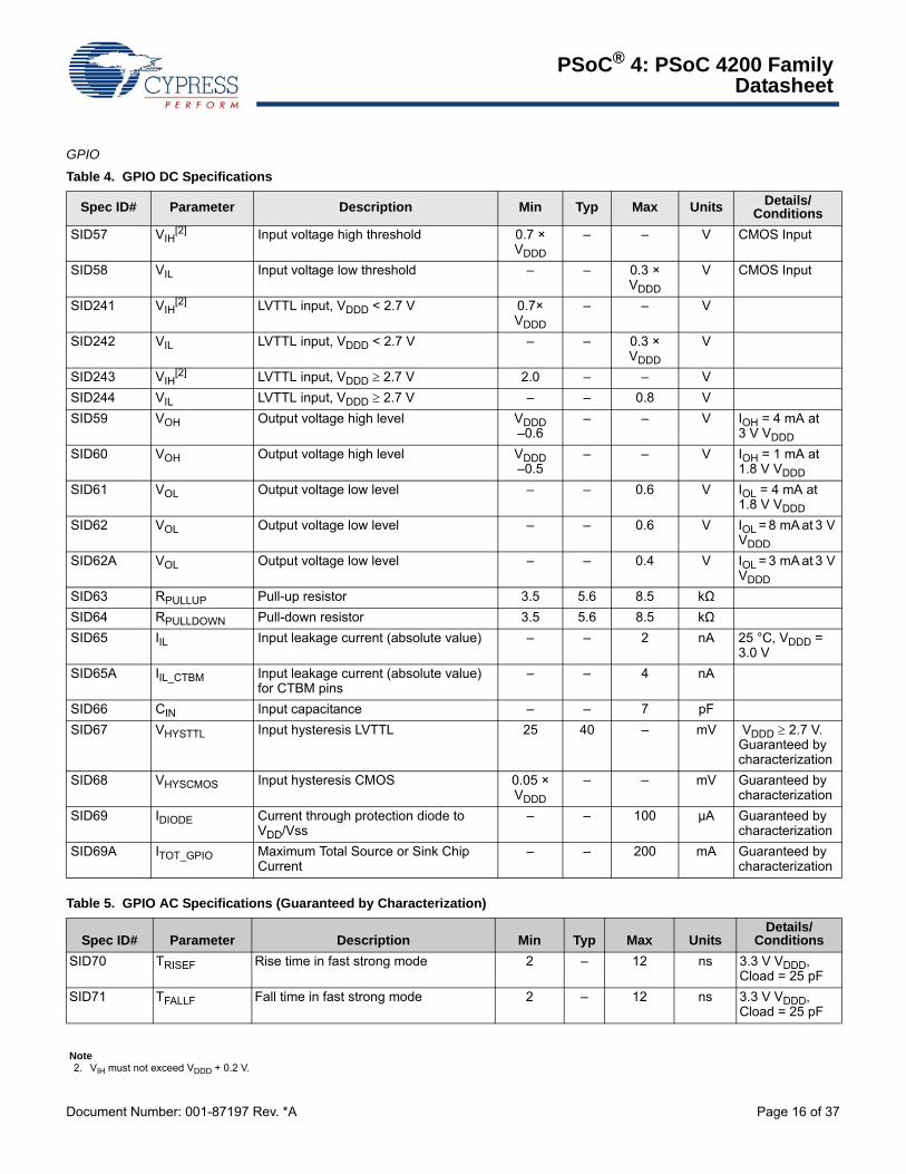
Table 4. GPIO DC Specifications
Spec ID# Parameter Description Min Typ Max Units Details/Conditions
SID57 VIH[2] Input voltage high threshold 0.7 ×
VDDD
– – V CMOS Input
SID58 VIL Input voltage low threshold – – 0.3 × VDDD
V CMOS Input
SID241 VIH[2] LVTTL input, VDDD < 2.7 V 0.7×
VDDD
– – V
SID242 VIL LVTTL input, VDDD < 2.7 V – – 0.3 × VDDD
V
SID243 VIH[2] LVTTL input, VDDD ≥ 2.7 V 2.0 – – V
SID244 VIL LVTTL input, VDDD ≥ 2.7 V – – 0.8 VSID59 VOH Output voltage high level VDDD
–0.6– – V IOH = 4 mA at
3 V VDDDSID60 VOH Output voltage high level VDDD
–0.5– – V IOH = 1 mA at
1.8 V VDDDSID61 VOL Output voltage low level – – 0.6 V IOL = 4 mA at
1.8 V VDDDSID62 VOL Output voltage low level – – 0.6 V IOL = 8 mA at 3 V
VDDDSID62A VOL Output voltage low level – – 0.4 V IOL = 3 mA at 3 V
VDDDSID63 RPULLUP Pull-up resistor 3.5 5.6 8.5 kΩSID64 RPULLDOWN Pull-down resistor 3.5 5.6 8.5 kΩSID65 IIL Input leakage current (absolute value) – – 2 nA 25 °C, VDDD =
3.0 VSID65A IIL_CTBM Input leakage current (absolute value)
for CTBM pins– – 4 nA
SID66 CIN Input capacitance – – 7 pFSID67 VHYSTTL Input hysteresis LVTTL 25 40 – mV VDDD ≥ 2.7 V.
Guaranteed by characterization
SID68 VHYSCMOS Input hysteresis CMOS 0.05 × VDDD
– – mV Guaranteed by characterization
SID69 IDIODE Current through protection diode to VDD/Vss
– – 100 µA Guaranteed by characterization
SID69A ITOT_GPIO Maximum Total Source or Sink Chip Current
– – 200 mA Guaranteed by characterization
Table 5. GPIO AC Specifications (Guaranteed by Characterization)
Spec ID# Parameter Description Min Typ Max UnitsDetails/
ConditionsSID70 TRISEF Rise time in fast strong mode 2 – 12 ns 3.3 V VDDD,
Cload = 25 pFSID71 TFALLF Fall time in fast strong mode 2 – 12 ns 3.3 V VDDD,
Cload = 25 pF
PSoC® 4: PSoC 4200 FamilyDatasheet
Document Number: 001-87197 Rev. *A Page 17 of 37
XRES
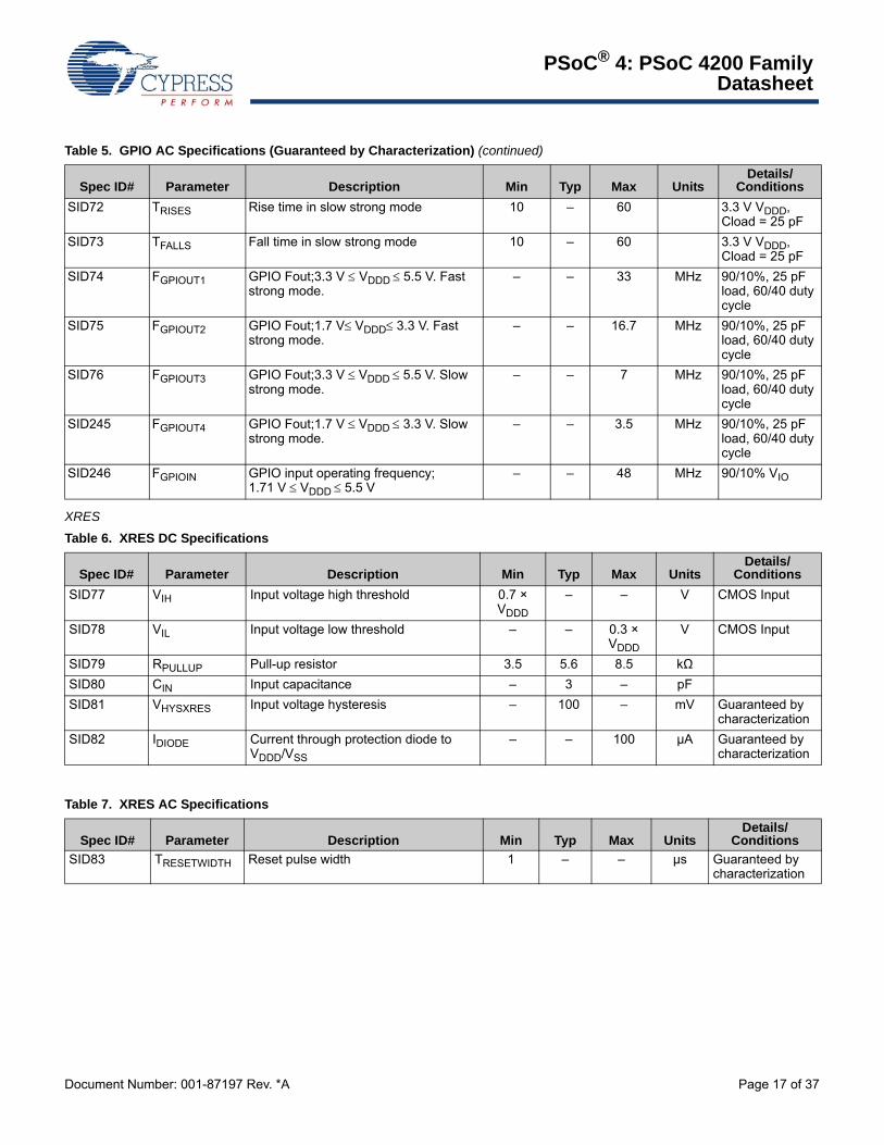
SID72 TRISES Rise time in slow strong mode 10 – 60 3.3 V VDDD, Cload = 25 pF
SID73 TFALLS Fall time in slow strong mode 10 – 60 3.3 V VDDD, Cload = 25 pF
SID74 FGPIOUT1 GPIO Fout;3.3 V ≤ VDDD ≤ 5.5 V. Fast strong mode.
– – 33 MHz 90/10%, 25 pF load, 60/40 duty cycle
SID75 FGPIOUT2 GPIO Fout;1.7 V≤ VDDD≤ 3.3 V. Fast strong mode.
– – 16.7 MHz 90/10%, 25 pF load, 60/40 duty cycle
SID76 FGPIOUT3 GPIO Fout;3.3 V ≤ VDDD ≤ 5.5 V. Slow strong mode.
– – 7 MHz 90/10%, 25 pF load, 60/40 duty cycle
SID245 FGPIOUT4 GPIO Fout;1.7 V ≤ VDDD ≤ 3.3 V. Slow strong mode.
– – 3.5 MHz 90/10%, 25 pF load, 60/40 duty cycle
SID246 FGPIOIN GPIO input operating frequency;1.71 V ≤ VDDD ≤ 5.5 V
– – 48 MHz 90/10% VIO
Table 5. GPIO AC Specifications (Guaranteed by Characterization) (continued)
Spec ID# Parameter Description Min Typ Max UnitsDetails/
Conditions
Table 6. XRES DC Specifications
Spec ID# Parameter Description Min Typ Max UnitsDetails/
ConditionsSID77 VIH Input voltage high threshold 0.7 ×
VDDD
– – V CMOS Input
SID78 VIL Input voltage low threshold – – 0.3 × VDDD
V CMOS Input
SID79 RPULLUP Pull-up resistor 3.5 5.6 8.5 kΩSID80 CIN Input capacitance – 3 – pFSID81 VHYSXRES Input voltage hysteresis – 100 – mV Guaranteed by
characterizationSID82 IDIODE Current through protection diode to
VDDD/VSS
– – 100 µA Guaranteed by characterization
Table 7. XRES AC Specifications
Spec ID# Parameter Description Min Typ Max UnitsDetails/
ConditionsSID83 TRESETWIDTH Reset pulse width 1 – – µs Guaranteed by
characterization
PSoC® 4: PSoC 4200 FamilyDatasheet
Document Number: 001-87197 Rev. *A Page 18 of 37
Analog Peripherals
Opamp
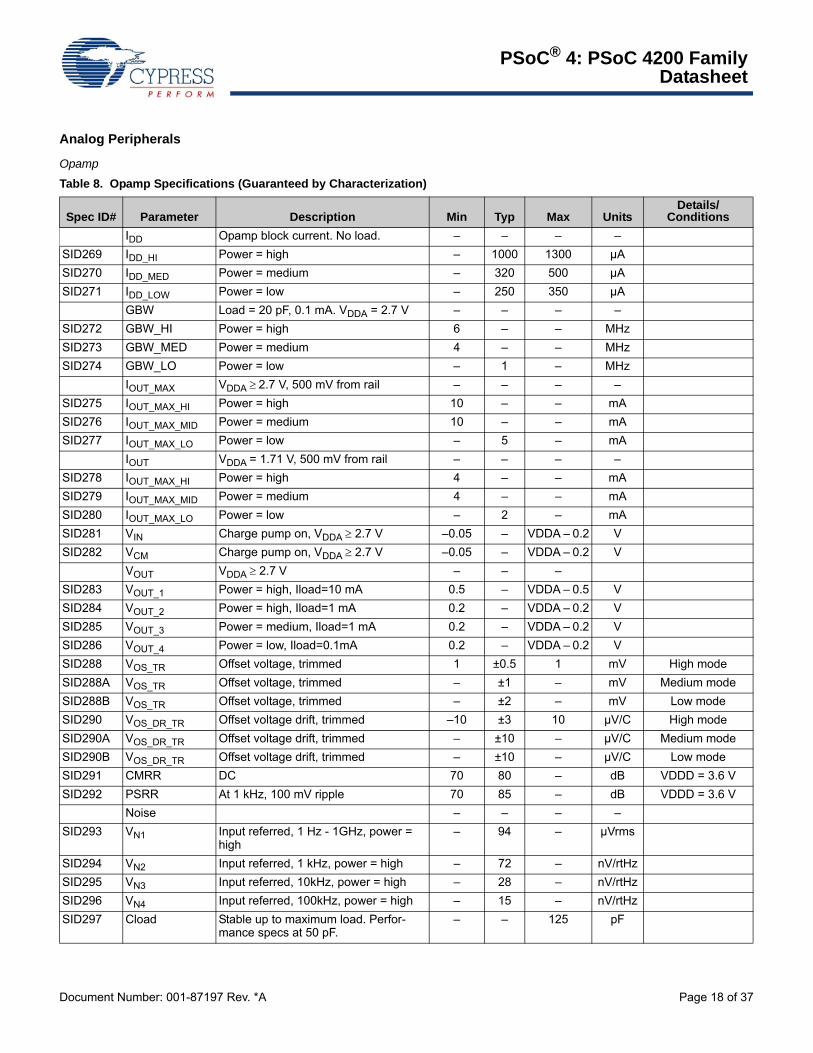
Table 8. Opamp Specifications (Guaranteed by Characterization)
Spec ID# Parameter Description Min Typ Max UnitsDetails/
ConditionsIDD Opamp block current. No load. – – – –
SID269 IDD_HI Power = high – 1000 1300 µASID270 IDD_MED Power = medium – 320 500 µASID271 IDD_LOW Power = low – 250 350 µA
GBW Load = 20 pF, 0.1 mA. VDDA = 2.7 V – – – –SID272 GBW_HI Power = high 6 – – MHzSID273 GBW_MED Power = medium 4 – – MHzSID274 GBW_LO Power = low – 1 – MHz
IOUT_MAX VDDA ≥ 2.7 V, 500 mV from rail – – – –SID275 IOUT_MAX_HI Power = high 10 – – mASID276 IOUT_MAX_MID Power = medium 10 – – mASID277 IOUT_MAX_LO Power = low – 5 – mA
IOUT VDDA = 1.71 V, 500 mV from rail – – – –SID278 IOUT_MAX_HI Power = high 4 – – mASID279 IOUT_MAX_MID Power = medium 4 – – mASID280 IOUT_MAX_LO Power = low – 2 – mASID281 VIN Charge pump on, VDDA ≥ 2.7 V –0.05 – VDDA – 0.2 VSID282 VCM Charge pump on, VDDA ≥ 2.7 V –0.05 – VDDA – 0.2 V
VOUT VDDA ≥ 2.7 V – – –SID283 VOUT_1 Power = high, Iload=10 mA 0.5 – VDDA – 0.5 VSID284 VOUT_2 Power = high, Iload=1 mA 0.2 – VDDA – 0.2 VSID285 VOUT_3 Power = medium, Iload=1 mA 0.2 – VDDA – 0.2 VSID286 VOUT_4 Power = low, Iload=0.1mA 0.2 – VDDA – 0.2 VSID288 VOS_TR Offset voltage, trimmed 1 ±0.5 1 mV High modeSID288A VOS_TR Offset voltage, trimmed – ±1 – mV Medium modeSID288B VOS_TR Offset voltage, trimmed – ±2 – mV Low modeSID290 VOS_DR_TR Offset voltage drift, trimmed –10 ±3 10 µV/C High modeSID290A VOS_DR_TR Offset voltage drift, trimmed – ±10 – µV/C Medium modeSID290B VOS_DR_TR Offset voltage drift, trimmed – ±10 – µV/C Low modeSID291 CMRR DC 70 80 – dB VDDD = 3.6 VSID292 PSRR At 1 kHz, 100 mV ripple 70 85 – dB VDDD = 3.6 V
Noise – – – –SID293 VN1 Input referred, 1 Hz - 1GHz, power =
high– 94 – µVrms
SID294 VN2 Input referred, 1 kHz, power = high – 72 – nV/rtHzSID295 VN3 Input referred, 10kHz, power = high – 28 – nV/rtHzSID296 VN4 Input referred, 100kHz, power = high – 15 – nV/rtHzSID297 Cload Stable up to maximum load. Perfor-
mance specs at 50 pF.– – 125 pF
PSoC® 4: PSoC 4200 FamilyDatasheet
Document Number: 001-87197 Rev. *A Page 19 of 37
Comparator
SID298 Slew_rate Cload = 50 pF, Power = High, VDDA ≥ 2.7 V
6 – – V/µsec
SID299 T_op_wake From disable to enable, no external RC dominating
– 300 – µsec
Comp_mode Comparator mode; 50 mV drive, Trise = Tfall (approx.)
– – –
SID300 TPD1 Response time; power = high – 150 – nsecSID301 TPD2 Response time; power = medium – 400 – nsecSID302 TPD3 Response time; power = low – 2000 – nsecSID303 Vhyst_op Hysteresis – 10 – mV
Table 8. Opamp Specifications (Guaranteed by Characterization) (continued)
Spec ID# Parameter Description Min Typ Max UnitsDetails/
Conditions
Table 9. Comparator DC Specifications
Spec ID# Parameter Description Min Typ Max UnitsDetails/
ConditionsSID85 VOFFSET2 Input offset voltage, trimmed – – ±4 mVSID86 VHYST Hysteresis when enabled – 10 35 mV Guaranteed by
characterizationSID87 VICM1 Input common mode voltage in normal
mode0 – VDDD – 0.1 V Modes 1 and 2.
Guaranteed by characterization
SID247 VICM2 Input common mode voltage in low power mode
0 – VDDD V Guaranteed by characterization
SID247A VICM2 Input common mode voltage in ultra low power mode
0 – VDDD – 1.15
V Guaranteed by characterization
SID88 CMRR Common mode rejection ratio 50 – – dB VDDD ≥ 2.7 V. Guaranteed by characterization
SID88A CMRR Common mode rejection ratio 42 – – dB VDDD < 2.7 V. Guaranteed by characterization
SID89 ICMP1 Block current, normal mode – – 280 µA Guaranteed by characterization
SID248 ICMP2 Block current, low power mode – – 50 µA Guaranteed by characterization
SID259 ICMP3 Block current, ultra low power mode – – 6 µA Guaranteed by characterization
SID90 ZCMP DC input impedance of comparator 35 – – MΩ Guaranteed by characterization
Table 10. Comparator AC Specifications (Guaranteed by Characterization)
Spec ID# Parameter Description Min Typ Max Units Details/ConditionsSID91 TRESP1 Response time, normal mode – – 38 ns 50 mV overdriveSID258 TRESP2 Response time, low power mode – – 70 ns 50 mV overdriveSID92 TRESP3 Response time, ultra low power mode – – 2.3 µs 200 mV overdrive
PSoC® 4: PSoC 4200 FamilyDatasheet
Document Number: 001-87197 Rev. *A Page 20 of 37
Temperature Sensor
SAR ADC
Table 11. Temperature Sensor Specifications
Spec ID# Parameter Description Min Typ Max Units Details/ConditionsSID93 TSENSACC Temperature sensor accuracy –5 ±1 +5 °C –40 to +85 °C
Table 12. SAR ADC DC Specifications
Spec ID# Parameter Description Min Typ Max Units Details/ConditionsSID94 A_RES Resolution – – 12 bits
SID95 A_CHNIS_S Number of channels - single ended – – 8 8 full speed
SID96 A-CHNKS_D Number of channels - differential – – 4 Diff inputs use neighboring I/O
SID97 A-MONO Monotonicity – – – Yes. Based on characterization
SID98 A_GAINERR Gain error – – ±0.1 % With external reference. Guaranteed by characterization
SID99 A_OFFSET Input offset voltage – – 2 mV Measured with 1-V VREF. Guaranteed by characterization
SID100 A_ISAR Current consumption – – 1 mA
SID101 A_VINS Input voltage range - single ended VSS – VDDA V Based on device characterization
SID102 A_VIND Input voltage range - differential VSS – VDDA V Based on device characterization
SID103 A_INRES Input resistance – – 2.2 KΩ Based on device characterization
SID104 A_INCAP Input capacitance – – 10 pF Based on device characterization
Table 13. SAR ADC AC Specifications (Guaranteed by Characterization)
Spec ID# Parameter Description Min Typ Max Units Details/ConditionsSID106 A_PSRR Power supply rejection ratio 70 – – dBSID107 A_CMRR Common mode rejection ratio 66 – – dB Measured at 1 VSID108 A_SAMP Sample rate – – 1 MspsSID109 A_SNDR Signal-to-noise and distortion ratio
(SINAD)65 – – dB FIN = 10 kHz
SID111 A_INL Integral non linearity –1.7 – +2 LSB VDD = 1.71 to 5.5, 1 Msps, Vref = 1 to 5.5.
SID111A A_INL Integral non linearity –1.5 – +1.7 LSB VDDD = 1.71 to 3.6, 1 Msps, Vref = 1.71 to VDDD.
SID111B A_INL Integral non linearity –1.5 – +1.7 LSB VDDD = 1.71 to 5.5, 500 Ksps, Vref = 1 to 5.5.
PSoC® 4: PSoC 4200 FamilyDatasheet
Document Number: 001-87197 Rev. *A Page 21 of 37
CSD
SID112 A_DNL Differential non linearity –1 – +2.2 LSB VDDD = 1.71 to 5.5, 1 Msps, Vref = 1 to 5.5.
SID112A A_DNL Differential non linearity –1 – +2 LSB VDDD = 1.71 to 3.6, 1 Msps, Vref = 1.71 to VDDD.
SID112B A_DNL Differential non linearity –1 – +2.2 LSB VDDD = 1.71 to 5.5, 500 Ksps, Vref = 1 to 5.5.
SID113 A_THD Total harmonic distortion – – –65 dB FIN = 10 kHz.
Table 13. SAR ADC AC Specifications (Guaranteed by Characterization) (continued)
Spec ID# Parameter Description Min Typ Max Units Details/Conditions
Table 14. CSD Block Specification
Spec ID# Parameter Description Min Typ Max UnitsDetails/
Conditions
CSD SpecificationSID308 VCSD Voltage range of operation 1.71 – 5.5 V
SID309 IDAC1 DNL for 8-bit resolution –1 – 1 LSB
SID310 IDAC1 INL for 8-bit resolution –3 – 3 LSB
SID311 IDAC2 DNL for 7-bit resolution –1 – 1 LSB
SID312 IDAC2 INL for 7-bit resolution –3 – 3 LSB
SID313 SNR Ratio of counts of finger to noise. Guaranteed by characterization
5 – – Ratio Capacitance range of 9 to 35 pF, 0.1 pF sensitivity
SID314 IDAC1_CRT1 Output current of Idac1 (8-bits) in High range
– 612 – µA
SID314A IDAC1_CRT2 Output current of Idac1(8-bits) in Low range
– 306 – µA
SID315 IDAC2_CRT1 Output current of Idac2 (7-bits) in High range
– 304.8 – µA
SID315A IDAC2_CRT2 Output current of Idac2 (7-bits) in Low range
– 152.4 – µA
PSoC® 4: PSoC 4200 FamilyDatasheet
Document Number: 001-87197 Rev. *A Page 22 of 37
Digital PeripheralsThe following specifications apply to the Timer/Counter/PWM peripheral in timer mode.
Timer
Counter
Pulse Width Modulation (PWM)
Table 15. Timer DC Specifications (Guaranteed by Characterization)Spec ID Parameter Description Min Typ Max Units Details/Conditions
SID115 ITIM1 Block current consumption at 3 MHz – – 19 µA 16-bit timerSID116 ITIM2 Block current consumption at 12 MHz – – 66 µA 16-bit timerSID117 ITIM3 Block current consumption at 48 MHz – – 285 µA 16-bit timer
Table 16. Timer AC Specifications (Guaranteed by Characterization)Spec ID Parameter Description Min Typ Max Units Details/Conditions
SID118 TTIMFREQ Operating frequency – – 48 MHzSID119 TCAPWINT Capture pulse width (internal) 42 – – nsSID120 TCAPWEXT Capture pulse width (external) 42 – – nsSID121 TTIMRES Timer resolution 21 – – nsSID122 TTENWIDINT Enable pulse width (internal) 42 – – nsSID123 TTENWIDEXT Enable pulse width (external) 42 – – nsSID124 TTIMRESWINT Reset pulse width (internal) 42 – – nsSID125 TTIMRESEXT Reset pulse width (external) 42 – – ns
Table 17. Counter DC Specifications (Guaranteed by Characterization)Spec ID Parameter Description Min Typ Max Units Details/Conditions
SID126 ICTR1 Block current consumption at 3 MHz – – 19 µA 16-bit CounterSID127 ICTR2 Block current consumption at 12 MHz – – 66 µA 16-bit CounterSID128 ICTR3 Block current consumption at 48 MHz – – 285 µA 16-bit Counter
Table 18. Counter AC Specifications (Guaranteed by Characterization)Spec ID Parameter Description Min Typ Max Units Details/Conditions
SID129 TCTRFREQ Operating frequency – – 48 MHzSID130 TCTRPWINT Capture pulse width (internal) 42 – – nsSID131 TCTRPWEXT Capture pulse width (external) 42 – – nsSID132 TCTRES Counter Resolution 21 – – nsSID133 TCENWIDINT Enable pulse width (internal) 42 – – nsSID134 TCENWIDEXT Enable pulse width (external) 42 – – nsSID135 TCTRRESWINT Reset pulse width (internal) 42 – – nsSID136 TCTRRESWEXT Reset pulse width (external) 42 – – ns
Table 19. PWM DC Specifications (Guaranteed by Characterization)
Spec ID Parameter Description Min Typ Max Units Details/ConditionsSID137 IPWM1 Block current consumption at 3 MHz – – 19 µA 16-bit PWMSID138 IPWM2 Block current consumption at 12 MHz – – 66 µA 16-bit PWMSID139 IPWM3 Block current consumption at 48 MHz – – 285 µA 16-bit PWM
PSoC® 4: PSoC 4200 FamilyDatasheet
Document Number: 001-87197 Rev. *A Page 23 of 37
I2C
LCD Direct Drive
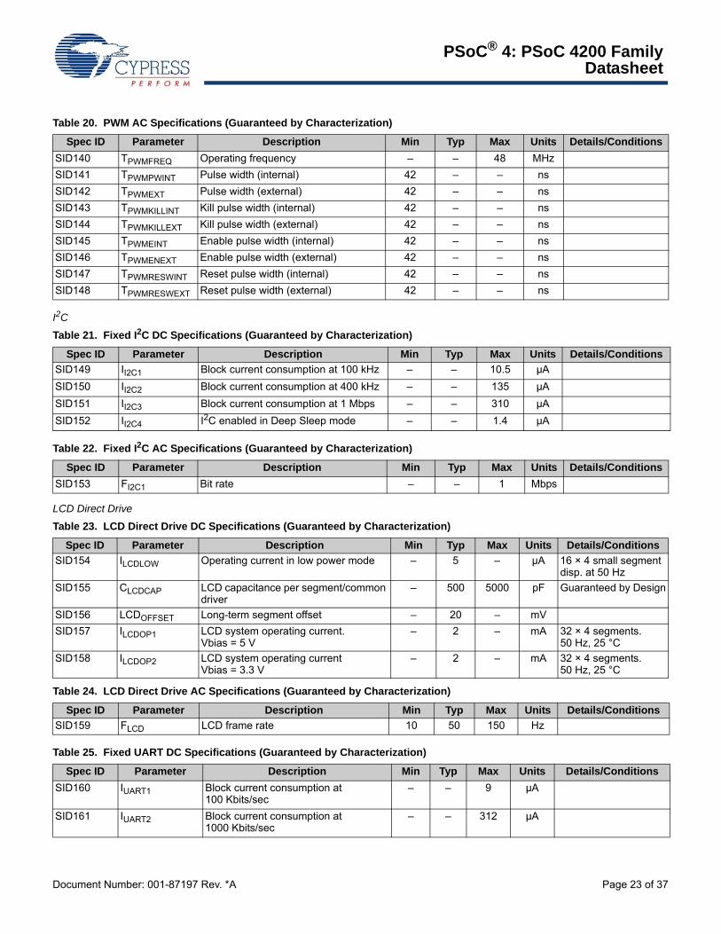
Table 20. PWM AC Specifications (Guaranteed by Characterization)
Spec ID Parameter Description Min Typ Max Units Details/ConditionsSID140 TPWMFREQ Operating frequency – – 48 MHzSID141 TPWMPWINT Pulse width (internal) 42 – – nsSID142 TPWMEXT Pulse width (external) 42 – – nsSID143 TPWMKILLINT Kill pulse width (internal) 42 – – nsSID144 TPWMKILLEXT Kill pulse width (external) 42 – – nsSID145 TPWMEINT Enable pulse width (internal) 42 – – nsSID146 TPWMENEXT Enable pulse width (external) 42 – – nsSID147 TPWMRESWINT Reset pulse width (internal) 42 – – nsSID148 TPWMRESWEXT Reset pulse width (external) 42 – – ns
Table 21. Fixed I2C DC Specifications (Guaranteed by Characterization)
Spec ID Parameter Description Min Typ Max Units Details/ConditionsSID149 II2C1 Block current consumption at 100 kHz – – 10.5 µASID150 II2C2 Block current consumption at 400 kHz – – 135 µASID151 II2C3 Block current consumption at 1 Mbps – – 310 µASID152 II2C4 I2C enabled in Deep Sleep mode – – 1.4 µA
Table 22. Fixed I2C AC Specifications (Guaranteed by Characterization)
Spec ID Parameter Description Min Typ Max Units Details/ConditionsSID153 FI2C1 Bit rate – – 1 Mbps
Table 23. LCD Direct Drive DC Specifications (Guaranteed by Characterization)
Spec ID Parameter Description Min Typ Max Units Details/ConditionsSID154 ILCDLOW Operating current in low power mode – 5 – µA 16 × 4 small segment
disp. at 50 HzSID155 CLCDCAP LCD capacitance per segment/common
driver– 500 5000 pF Guaranteed by Design
SID156 LCDOFFSET Long-term segment offset – 20 – mVSID157 ILCDOP1 LCD system operating current.
Vbias = 5 V– 2 – mA 32 × 4 segments.
50 Hz, 25 °CSID158 ILCDOP2 LCD system operating current
Vbias = 3.3 V– 2 – mA 32 × 4 segments.
50 Hz, 25 °C
Table 24. LCD Direct Drive AC Specifications (Guaranteed by Characterization)
Spec ID Parameter Description Min Typ Max Units Details/ConditionsSID159 FLCD LCD frame rate 10 50 150 Hz
Table 25. Fixed UART DC Specifications (Guaranteed by Characterization)
Spec ID Parameter Description Min Typ Max Units Details/ConditionsSID160 IUART1 Block current consumption at
100 Kbits/sec– – 9 µA
SID161 IUART2 Block current consumption at 1000 Kbits/sec
– – 312 µA
PSoC® 4: PSoC 4200 FamilyDatasheet
Document Number: 001-87197 Rev. *A Page 24 of 37
SPI Specifications
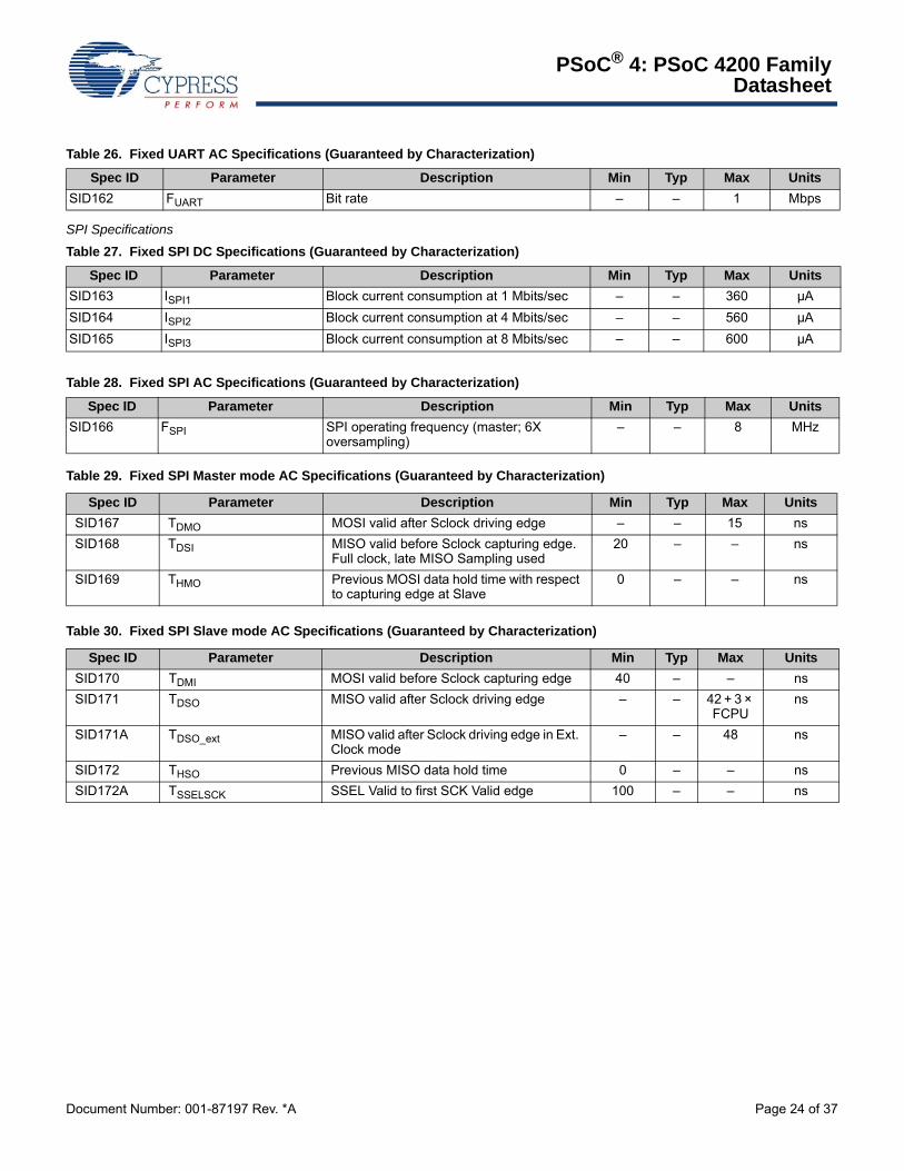
Table 26. Fixed UART AC Specifications (Guaranteed by Characterization)
Spec ID Parameter Description Min Typ Max UnitsSID162 FUART Bit rate – – 1 Mbps
Table 27. Fixed SPI DC Specifications (Guaranteed by Characterization)
Spec ID Parameter Description Min Typ Max UnitsSID163 ISPI1 Block current consumption at 1 Mbits/sec – – 360 µASID164 ISPI2 Block current consumption at 4 Mbits/sec – – 560 µASID165 ISPI3 Block current consumption at 8 Mbits/sec – – 600 µA
Table 28. Fixed SPI AC Specifications (Guaranteed by Characterization)
Spec ID Parameter Description Min Typ Max UnitsSID166 FSPI SPI operating frequency (master; 6X
oversampling)– – 8 MHz
Table 29. Fixed SPI Master mode AC Specifications (Guaranteed by Characterization)
Spec ID Parameter Description Min Typ Max UnitsSID167 TDMO MOSI valid after Sclock driving edge – – 15 nsSID168 TDSI MISO valid before Sclock capturing edge.
Full clock, late MISO Sampling used20 – – ns
SID169 THMO Previous MOSI data hold time with respect to capturing edge at Slave
0 – – ns
Table 30. Fixed SPI Slave mode AC Specifications (Guaranteed by Characterization)
Spec ID Parameter Description Min Typ Max UnitsSID170 TDMI MOSI valid before Sclock capturing edge 40 – – nsSID171 TDSO MISO valid after Sclock driving edge – – 42 + 3 ×
FCPUns
SID171A TDSO_ext MISO valid after Sclock driving edge in Ext. Clock mode
– – 48 ns
SID172 THSO Previous MISO data hold time 0 – – nsSID172A TSSELSCK SSEL Valid to first SCK Valid edge 100 – – ns
PSoC® 4: PSoC 4200 FamilyDatasheet
Document Number: 001-87197 Rev. *A Page 25 of 37
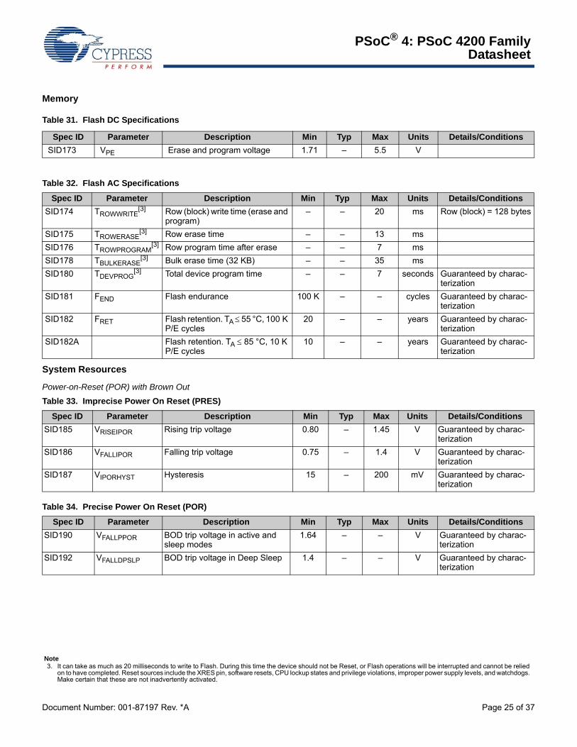
Memory
System Resources
Power-on-Reset (POR) with Brown Out
Table 31. Flash DC Specifications
Spec ID Parameter Description Min Typ Max Units Details/ConditionsSID173 VPE Erase and program voltage 1.71 – 5.5 V
Note3. It can take as much as 20 milliseconds to write to Flash. During this time the device should not be Reset, or Flash operations will be interrupted and cannot be relied
on to have completed. Reset sources include the XRES pin, software resets, CPU lockup states and privilege violations, improper power supply levels, and watchdogs. Make certain that these are not inadvertently activated.
Table 32. Flash AC Specifications
Spec ID Parameter Description Min Typ Max Units Details/ConditionsSID174 TROWWRITE
[3] Row (block) write time (erase and program)
– – 20 ms Row (block) = 128 bytes
SID175 TROWERASE[3] Row erase time – – 13 ms
SID176 TROWPROGRAM[3] Row program time after erase – – 7 ms
SID178 TBULKERASE[3] Bulk erase time (32 KB) – – 35 ms
SID180 TDEVPROG[3] Total device program time – – 7 seconds Guaranteed by charac-
terizationSID181 FEND Flash endurance 100 K – – cycles Guaranteed by charac-
terizationSID182 FRET Flash retention. TA ≤ 55 °C, 100 K
P/E cycles20 – – years Guaranteed by charac-
terizationSID182A Flash retention. TA ≤ 85 °C, 10 K
P/E cycles10 – – years Guaranteed by charac-
terization
Table 33. Imprecise Power On Reset (PRES)
Spec ID Parameter Description Min Typ Max Units Details/ConditionsSID185 VRISEIPOR Rising trip voltage 0.80 – 1.45 V Guaranteed by charac-
terizationSID186 VFALLIPOR Falling trip voltage 0.75 – 1.4 V Guaranteed by charac-
terizationSID187 VIPORHYST Hysteresis 15 – 200 mV Guaranteed by charac-
terization
Table 34. Precise Power On Reset (POR)
Spec ID Parameter Description Min Typ Max Units Details/ConditionsSID190 VFALLPPOR BOD trip voltage in active and
sleep modes1.64 – – V Guaranteed by charac-
terizationSID192 VFALLDPSLP BOD trip voltage in Deep Sleep 1.4 – – V Guaranteed by charac-
terization
PSoC® 4: PSoC 4200 FamilyDatasheet
Document Number: 001-87197 Rev. *A Page 26 of 37
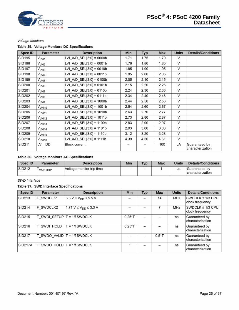
Voltage Monitors
SWD Interface
Table 35. Voltage Monitors DC Specifications
Spec ID Parameter Description Min Typ Max Units Details/ConditionsSID195 VLVI1 LVI_A/D_SEL[3:0] = 0000b 1.71 1.75 1.79 VSID196 VLVI2 LVI_A/D_SEL[3:0] = 0001b 1.76 1.80 1.85 VSID197 VLVI3 LVI_A/D_SEL[3:0] = 0010b 1.85 1.90 1.95 VSID198 VLVI4 LVI_A/D_SEL[3:0] = 0011b 1.95 2.00 2.05 VSID199 VLVI5 LVI_A/D_SEL[3:0] = 0100b 2.05 2.10 2.15 VSID200 VLVI6 LVI_A/D_SEL[3:0] = 0101b 2.15 2.20 2.26 VSID201 VLVI7 LVI_A/D_SEL[3:0] = 0110b 2.24 2.30 2.36 VSID202 VLVI8 LVI_A/D_SEL[3:0] = 0111b 2.34 2.40 2.46 VSID203 VLVI9 LVI_A/D_SEL[3:0] = 1000b 2.44 2.50 2.56 VSID204 VLVI10 LVI_A/D_SEL[3:0] = 1001b 2.54 2.60 2.67 VSID205 VLVI11 LVI_A/D_SEL[3:0] = 1010b 2.63 2.70 2.77 VSID206 VLVI12 LVI_A/D_SEL[3:0] = 1011b 2.73 2.80 2.87 VSID207 VLVI13 LVI_A/D_SEL[3:0] = 1100b 2.83 2.90 2.97 VSID208 VLVI14 LVI_A/D_SEL[3:0] = 1101b 2.93 3.00 3.08 VSID209 VLVI15 LVI_A/D_SEL[3:0] = 1110b 3.12 3.20 3.28 VSID210 VLVI16 LVI_A/D_SEL[3:0] = 1111b 4.39 4.50 4.61 VSID211 LVI_IDD Block current – – 100 µA Guaranteed by
characterization
Table 36. Voltage Monitors AC Specifications
Spec ID Parameter Description Min Typ Max Units Details/ConditionsSID212 TMONTRIP Voltage monitor trip time – – 1 µs Guaranteed by
characterization
Table 37. SWD Interface Specifications
Spec ID Parameter Description Min Typ Max Units Details/ConditionsSID213 F_SWDCLK1 3.3 V ≤ VDD ≤ 5.5 V – – 14 MHz SWDCLK ≤ 1/3 CPU
clock frequencySID214 F_SWDCLK2 1.71 V ≤ VDD ≤ 3.3 V – – 7 MHz SWDCLK ≤ 1/3 CPU
clock frequencySID215 T_SWDI_SETUP T = 1/f SWDCLK 0.25*T – – ns Guaranteed by
characterizationSID216 T_SWDI_HOLD T = 1/f SWDCLK 0.25*T – – ns Guaranteed by
characterizationSID217 T_SWDO_VALID T = 1/f SWDCLK – – 0.5*T ns Guaranteed by
characterizationSID217A T_SWDO_HOLD T = 1/f SWDCLK 1 – – ns Guaranteed by
characterization
PSoC® 4: PSoC 4200 FamilyDatasheet
Document Number: 001-87197 Rev. *A Page 27 of 37
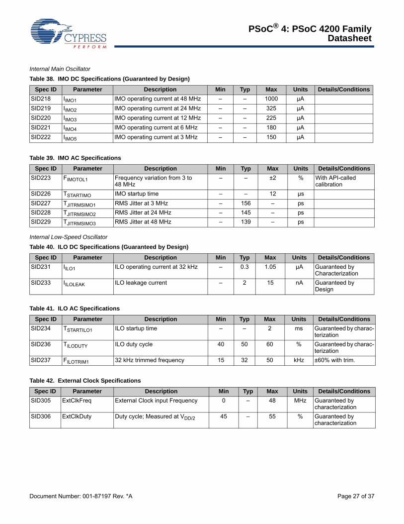
Internal Main Oscillator
Internal Low-Speed Oscillator
Table 38. IMO DC Specifications (Guaranteed by Design)
Spec ID Parameter Description Min Typ Max Units Details/ConditionsSID218 IIMO1 IMO operating current at 48 MHz – – 1000 µASID219 IIMO2 IMO operating current at 24 MHz – – 325 µASID220 IIMO3 IMO operating current at 12 MHz – – 225 µASID221 IIMO4 IMO operating current at 6 MHz – – 180 µASID222 IIMO5 IMO operating current at 3 MHz – – 150 µA
Table 39. IMO AC Specifications
Spec ID Parameter Description Min Typ Max Units Details/ConditionsSID223 FIMOTOL1 Frequency variation from 3 to
48 MHz– – ±2 % With API-called
calibrationSID226 TSTARTIMO IMO startup time – – 12 µsSID227 TJITRMSIMO1 RMS Jitter at 3 MHz – 156 – psSID228 TJITRMSIMO2 RMS Jitter at 24 MHz – 145 – psSID229 TJITRMSIMO3 RMS Jitter at 48 MHz – 139 – ps
Table 40. ILO DC Specifications (Guaranteed by Design)
Spec ID Parameter Description Min Typ Max Units Details/ConditionsSID231 IILO1 ILO operating current at 32 kHz – 0.3 1.05 µA Guaranteed by
CharacterizationSID233 IILOLEAK ILO leakage current – 2 15 nA Guaranteed by
Design
Table 41. ILO AC Specifications
Spec ID Parameter Description Min Typ Max Units Details/ConditionsSID234 TSTARTILO1 ILO startup time – – 2 ms Guaranteed by charac-
terizationSID236 TILODUTY ILO duty cycle 40 50 60 % Guaranteed by charac-
terizationSID237 FILOTRIM1 32 kHz trimmed frequency 15 32 50 kHz ±60% with trim.
Table 42. External Clock Specifications
Spec ID Parameter Description Min Typ Max Units Details/ConditionsSID305 ExtClkFreq External Clock input Frequency 0 – 48 MHz Guaranteed by
characterizationSID306 ExtClkDuty Duty cycle; Measured at VDD/2 45 – 55 % Guaranteed by
characterization
PSoC® 4: PSoC 4200 FamilyDatasheet
Document Number: 001-87197 Rev. *A Page 28 of 37
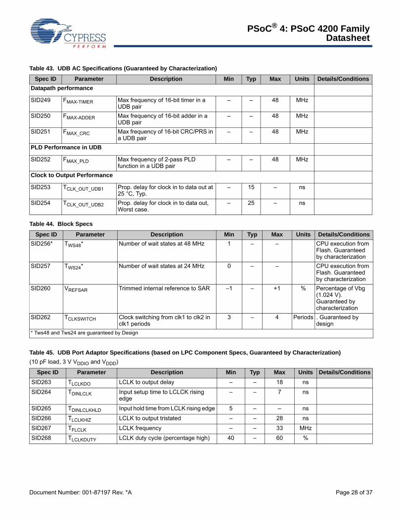
Table 43. UDB AC Specifications (Guaranteed by Characterization)
Spec ID Parameter Description Min Typ Max Units Details/ConditionsDatapath performance
SID249 FMAX-TIMER Max frequency of 16-bit timer in a UDB pair
– – 48 MHz
SID250 FMAX-ADDER Max frequency of 16-bit adder in a UDB pair
– – 48 MHz
SID251 FMAX_CRC Max frequency of 16-bit CRC/PRS in a UDB pair
– – 48 MHz
PLD Performance in UDB
SID252 FMAX_PLD Max frequency of 2-pass PLD function in a UDB pair
– – 48 MHz
Clock to Output Performance
SID253 TCLK_OUT_UDB1 Prop. delay for clock in to data out at 25 °C, Typ.
– 15 – ns
SID254 TCLK_OUT_UDB2 Prop. delay for clock in to data out, Worst case.
– 25 – ns
Table 44. Block Specs
Spec ID Parameter Description Min Typ Max Units Details/ConditionsSID256* TWS48* Number of wait states at 48 MHz 1 – – CPU execution from
Flash. Guaranteed by characterization
SID257 TWS24* Number of wait states at 24 MHz 0 – – CPU execution from Flash. Guaranteed by characterization
SID260 VREFSAR Trimmed internal reference to SAR –1 – +1 % Percentage of Vbg (1.024 V). Guaranteed by characterization
SID262 TCLKSWITCH Clock switching from clk1 to clk2 in clk1 periods
3 – 4 Periods . Guaranteed by design
* Tws48 and Tws24 are guaranteed by Design
Table 45. UDB Port Adaptor Specifications (based on LPC Component Specs, Guaranteed by Characterization)(10 pF load, 3 V VDDIO and VDDD)
Spec ID Parameter Description Min Typ Max Units Details/ConditionsSID263 TLCLKDO LCLK to output delay – – 18 ns
SID264 TDINLCLK Input setup time to LCLCK rising edge
– – 7 ns
SID265 TDINLCLKHLD Input hold time from LCLK rising edge 5 – – ns
SID266 TLCLKHIZ LCLK to output tristated – – 28 ns
SID267 TFLCLK LCLK frequency – – 33 MHz
SID268 TLCLKDUTY LCLK duty cycle (percentage high) 40 – 60 %
PSoC® 4: PSoC 4200 FamilyDatasheet
Document Number: 001-87197 Rev. *A Page 29 of 37
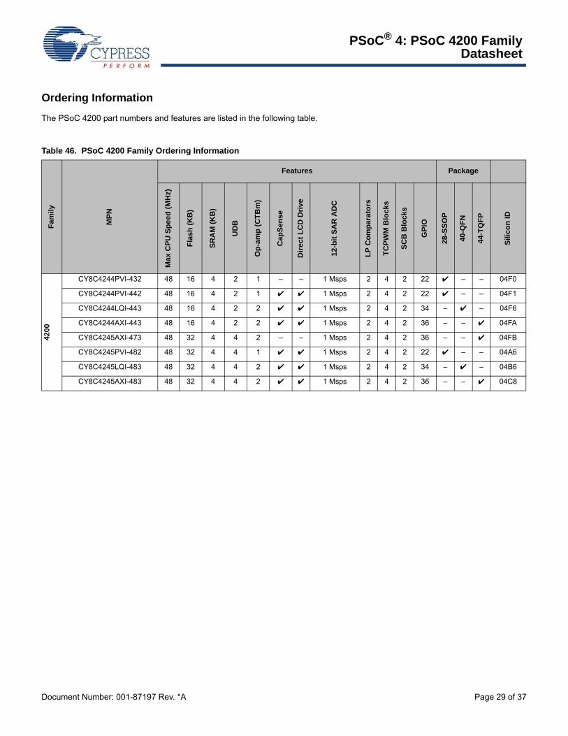
Ordering Information
The PSoC 4200 part numbers and features are listed in the following table.
Table 46. PSoC 4200 Family Ordering Information
Fam
ily
MPN
Features PackageM
ax C
PU S
peed
(MH
z)
Flas
h (K
B)
SRA
M (K
B)
UD
B
Op-
amp
(CTB
m)
Cap
Sens
e
Dire
ct L
CD
Driv
e
12-b
it SA
R A
DC
LP C
ompa
rato
rs
TCPW
M B
lock
s
SCB
Blo
cks
GPI
O
28-S
SOP
40-Q
FN
44-T
QFP
Silic
on ID
4200
CY8C4244PVI-432 48 16 4 2 1 – – 1 Msps 2 4 2 22 4 – – 04F0
CY8C4244PVI-442 48 16 4 2 1 4 4 1 Msps 2 4 2 22 4 – – 04F1
CY8C4244LQI-443 48 16 4 2 2 4 4 1 Msps 2 4 2 34 – 4 – 04F6
CY8C4244AXI-443 48 16 4 2 2 4 4 1 Msps 2 4 2 36 – – 4 04FA
CY8C4245AXI-473 48 32 4 4 2 – – 1 Msps 2 4 2 36 – – 4 04FB
CY8C4245PVI-482 48 32 4 4 1 4 4 1 Msps 2 4 2 22 4 – – 04A6
CY8C4245LQI-483 48 32 4 4 2 4 4 1 Msps 2 4 2 34 – 4 – 04B6
CY8C4245AXI-483 48 32 4 4 2 4 4 1 Msps 2 4 2 36 – – 4 04C8
PSoC® 4: PSoC 4200 FamilyDatasheet
Document Number: 001-87197 Rev. *A Page 30 of 37
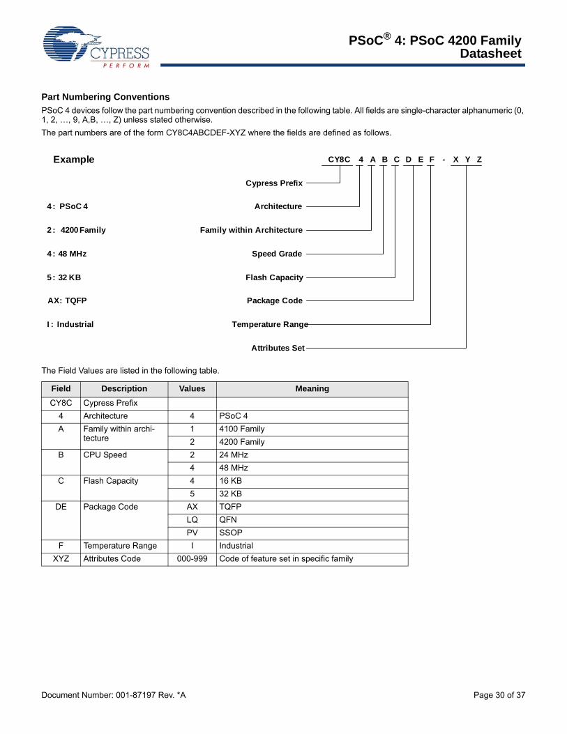
Part Numbering ConventionsPSoC 4 devices follow the part numbering convention described in the following table. All fields are single-character alphanumeric (0, 1, 2, …, 9, A,B, …, Z) unless stated otherwise. The part numbers are of the form CY8C4ABCDEF-XYZ where the fields are defined as follows.
The Field Values are listed in the following table.
Architecture
Cypress Prefix
Family within Architecture
Speed Grade
Flash Capacity
Package Code
Temperature Range
Attributes Set
4 : PSoC 4
4 : 48 MHz
5 : 32 KB
AX: TQFP
I : Industrial
Example CY8C 4 A EDCB F YX- Z
2 : 4200 Family
Field Description Values MeaningCY8C Cypress Prefix
4 Architecture 4 PSoC 4A Family within archi-
tecture1 4100 Family2 4200 Family
B CPU Speed 2 24 MHz4 48 MHz
C Flash Capacity 4 16 KB5 32 KB
DE Package Code AX TQFPLQ QFNPV SSOP
F Temperature Range I IndustrialXYZ Attributes Code 000-999 Code of feature set in specific family
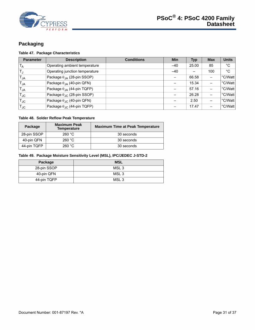
PSoC® 4: PSoC 4200 FamilyDatasheet
Document Number: 001-87197 Rev. *A Page 31 of 37
Packaging
Table 47. Package Characteristics
Parameter Description Conditions Min Typ Max UnitsTA Operating ambient temperature –40 25.00 85 °CTJ Operating junction temperature –40 – 100 °CTJA Package θJA (28-pin SSOP) – 66.58 – °C/WattTJA Package θJA (40-pin QFN) – 15.34 – °C/WattTJA Package θJA (44-pin TQFP) – 57.16 – °C/WattTJC Package θJC (28-pin SSOP) – 26.28 – °C/WattTJC Package θJC (40-pin QFN) – 2.50 – °C/WattTJC Package θJC (44-pin TQFP) – 17.47 – °C/Watt
Table 48. Solder Reflow Peak Temperature
Package Maximum Peak Temperature Maximum Time at Peak Temperature
28-pin SSOP 260 °C 30 seconds40-pin QFN 260 °C 30 seconds
44-pin TQFP 260 °C 30 seconds
Table 49. Package Moisture Sensitivity Level (MSL), IPC/JEDEC J-STD-2
Package MSL 28-pin SSOP MSL 340-pin QFN MSL 3 44-pin TQFP MSL 3
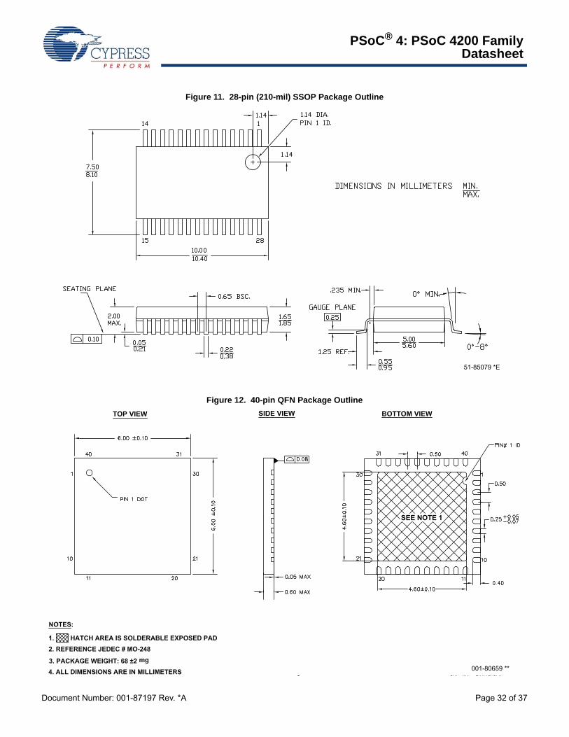
PSoC® 4: PSoC 4200 FamilyDatasheet
Document Number: 001-87197 Rev. *A Page 32 of 37
Figure 11. 28-pin (210-mil) SSOP Package Outline
Figure 12. 40-pin QFN Package Outline
51-85079 *E
001-80659 **
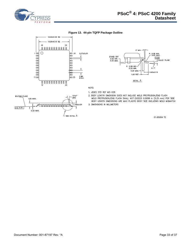
PSoC® 4: PSoC 4200 FamilyDatasheet
Document Number: 001-87197 Rev. *A Page 33 of 37
Figure 13. 44-pin TQFP Package Outline
51-85064 *E
PSoC® 4: PSoC 4200 FamilyDatasheet
Document Number: 001-87197 Rev. *A Page 34 of 37
Acronyms
Table 50. Acronyms Used in this Document
Acronym Descriptionabus analog local bus
ADC analog-to-digital converter
AG analog global
AHB AMBA (advanced microcontroller bus archi-tecture) high-performance bus, an ARM data transfer bus
ALU arithmetic logic unit
AMUXBUS analog multiplexer bus
API application programming interface
APSR application program status register
ARM® advanced RISC machine, a CPU architecture
ATM automatic thump mode
BW bandwidth
CAN Controller Area Network, a communications protocol
CMRR common-mode rejection ratio
CPU central processing unit
CRC cyclic redundancy check, an error-checking protocol
DAC digital-to-analog converter, see also IDAC, VDAC
DFB digital filter block
DIO digital input/output, GPIO with only digital capabilities, no analog. See GPIO.
DMIPS Dhrystone million instructions per second
DMA direct memory access, see also TD
DNL differential nonlinearity, see also INL
DNU do not use
DR port write data registers
DSI digital system interconnect
DWT data watchpoint and trace
ECC error correcting code
ECO external crystal oscillator
EEPROM electrically erasable programmable read-only memory
EMI electromagnetic interference
EMIF external memory interface
EOC end of conversion
EOF end of frame
EPSR execution program status register
ESD electrostatic discharge
ETM embedded trace macrocell
FIR finite impulse response, see also IIR
FPB flash patch and breakpoint
FS full-speed
GPIO general-purpose input/output, applies to a PSoC pin
HVI high-voltage interrupt, see also LVI, LVD
IC integrated circuit
IDAC current DAC, see also DAC, VDAC
IDE integrated development environment
I2C, or IIC Inter-Integrated Circuit, a communications protocol
IIR infinite impulse response, see also FIR
ILO internal low-speed oscillator, see also IMO
IMO internal main oscillator, see also ILO
INL integral nonlinearity, see also DNL
I/O input/output, see also GPIO, DIO, SIO, USBIO
IPOR initial power-on reset
IPSR interrupt program status register
IRQ interrupt request
ITM instrumentation trace macrocell
LCD liquid crystal display
LIN Local Interconnect Network, a communications protocol.
LR link register
LUT lookup table
LVD low-voltage detect, see also LVI
LVI low-voltage interrupt, see also HVI
LVTTL low-voltage transistor-transistor logic
MAC multiply-accumulate
MCU microcontroller unit
MISO master-in slave-out
NC no connect
NMI nonmaskable interrupt
NRZ non-return-to-zero
NVIC nested vectored interrupt controller
NVL nonvolatile latch, see also WOL
opamp operational amplifier
PAL programmable array logic, see also PLD
Table 50. Acronyms Used in this Document (continued)
Acronym Description
PSoC® 4: PSoC 4200 FamilyDatasheet
Document Number: 001-87197 Rev. *A Page 35 of 37
PC program counter
PCB printed circuit board
PGA programmable gain amplifier
PHUB peripheral hub
PHY physical layer
PICU port interrupt control unit
PLA programmable logic array
PLD programmable logic device, see also PAL
PLL phase-locked loop
PMDD package material declaration data sheet
POR power-on reset
PRES precise power-on reset
PRS pseudo random sequence
PS port read data register
PSoC® Programmable System-on-Chip™
PSRR power supply rejection ratio
PWM pulse-width modulator
RAM random-access memory
RISC reduced-instruction-set computing
RMS root-mean-square
RTC real-time clock
RTL register transfer language
RTR remote transmission request
RX receive
SAR successive approximation register
SC/CT switched capacitor/continuous time
SCL I2C serial clock
SDA I2C serial data
S/H sample and hold
SINAD signal to noise and distortion ratio
SIO special input/output, GPIO with advanced features. See GPIO.
SOC start of conversion
SOF start of frame
SPI Serial Peripheral Interface, a communications protocol
SR slew rate
SRAM static random access memory
SRES software reset
SWD serial wire debug, a test protocol
Table 50. Acronyms Used in this Document (continued)
Acronym DescriptionSWV single-wire viewer
TD transaction descriptor, see also DMA
THD total harmonic distortion
TIA transimpedance amplifier
TRM technical reference manual
TTL transistor-transistor logic
TX transmit
UART Universal Asynchronous Transmitter Receiver, a communications protocol
UDB universal digital block
USB Universal Serial Bus
USBIO USB input/output, PSoC pins used to connect to a USB port
VDAC voltage DAC, see also DAC, IDAC
WDT watchdog timer
WOL write once latch, see also NVL
WRES watchdog timer reset
XRES external reset I/O pin
XTAL crystal
Table 50. Acronyms Used in this Document (continued)
Acronym Description
PSoC® 4: PSoC 4200 FamilyDatasheet
Document Number: 001-87197 Rev. *A Page 36 of 37
Document ConventionsUnits of MeasureTable 51. Units of Measure
Symbol Unit of Measure°C degrees Celsius
dB decibel
fF femto farad
Hz hertz
KB 1024 bytes
kbps kilobits per second
Khr kilohour
kHz kilohertz
kΩ kilo ohm
ksps kilosamples per second
LSB least significant bit
Mbps megabits per second
MHz megahertz
MΩ mega-ohm
Msps megasamples per second
µA microampere
µF microfarad
µH microhenry
µs microsecond
µV microvolt
µW microwatt
mA milliampere
ms millisecond
mV millivolt
nA nanoampere
ns nanosecond
nV nanovolt
Ω ohm
pF picofarad
ppm parts per million
ps picosecond
s second
sps samples per second
sqrtHz square root of hertz
V volt
Document Number: 001-87197 Rev. *A Revised June 20, 2013 Page 37 of 37
All products and company names mentioned in this document may be the trademarks of their respective holders.
PSoC® 4: PSoC 4200 FamilyDatasheet
© Cypress Semiconductor Corporation, 2013. The information contained herein is subject to change without notice. Cypress Semiconductor Corporation assumes no responsibility for the use of anycircuitry other than circuitry embodied in a Cypress product. Nor does it convey or imply any license under patent or other rights. Cypress products are not warranted nor intended to be used for medical,life support, life saving, critical control or safety applications, unless pursuant to an express written agreement with Cypress. Furthermore, Cypress does not authorize its products for use as criticalcomponents in life-support systems where a malfunction or failure may reasonably be expected to result in significant injury to the user. The inclusion of Cypress products in life-support systemsapplication implies that the manufacturer assumes all risk of such use and in doing so indemnifies Cypress against all charges.
Any Source Code (software and/or firmware) is owned by Cypress Semiconductor Corporation (Cypress) and is protected by and subject to worldwide patent protection (United States and foreign),United States copyright laws and international treaty provisions. Cypress hereby grants to licensee a personal, non-exclusive, non-transferable license to copy, use, modify, create derivative works of,and compile the Cypress Source Code and derivative works for the sole purpose of creating custom software and or firmware in support of licensee product to be used only in conjunction with a Cypressintegrated circuit as specified in the applicable agreement. Any reproduction, modification, translation, compilation, or representation of this Source Code except as specified above is prohibited withoutthe express written permission of Cypress.
Disclaimer: CYPRESS MAKES NO WARRANTY OF ANY KIND, EXPRESS OR IMPLIED, WITH REGARD TO THIS MATERIAL, INCLUDING, BUT NOT LIMITED TO, THE IMPLIED WARRANTIESOF MERCHANTABILITY AND FITNESS FOR A PARTICULAR PURPOSE. Cypress reserves the right to make changes without further notice to the materials described herein. Cypress does notassume any liability arising out of the application or use of any product or circuit described herein. Cypress does not authorize its products for use as critical components in life-support systems wherea malfunction or failure may reasonably be expected to result in significant injury to the user. The inclusion of Cypress’ product in a life-support systems application implies that the manufacturerassumes all risk of such use and in doing so indemnifies Cypress against all charges.
Use may be limited by and subject to the applicable Cypress software license agreement.
Sales, Solutions, and Legal InformationWorldwide Sales and Design SupportCypress maintains a worldwide network of offices, solution centers, manufacturer’s representatives, and distributors. To find the office closest to you, visit us at Cypress Locations.
ProductsAutomotive cypress.com/go/automotiveClocks & Buffers cypress.com/go/clocksInterface cypress.com/go/interfaceLighting & Power Control cypress.com/go/powerpsoc
cypress.com/go/plcMemory cypress.com/go/memoryPSoC cypress.com/go/psocTouch Sensing cypress.com/go/touchUSB Controllers cypress.com/go/USBWireless/RF cypress.com/go/wireless
PSoC® Solutionspsoc.cypress.com/solutionsPSoC 1 | PSoC 3 | PSoC 4 | PSoC 5LP
Cypress Developer CommunityCommunity | Forums | Blogs | Video | Training
Technical Supportcypress.com/go/support