Embed Size (px)
Citation preview

PRELIMINARY
PSoC® 5: CY8C55 Family Datasheet
Programmable System-on-Chip (PSoC®)
Cypress Semiconductor Corporation • 198 Champion Court • San Jose, CA 95134-1709 • 408-943-2600
Document Number: 001-44094 Rev. *J Revised September 2, 2010
General DescriptionWith its unique array of configurable blocks, PSoC® 5 is a true system-level solution providing microcontroller unit (MCU), memory, analog, and digital peripheral functions in a single chip. The CY8C55 family offers a modern method of signal acquisition, signal processing, and control with high accuracy, high bandwidth, and high flexibility. Analog capability spans the range from thermocouples (near DC voltages) to ultrasonic signals. The CY8C55 family can handle dozens of data acquisition channels and analog inputs on every GPIO pin. The CY8C55 family is also a high-performance configurable digital system with some part numbers including interfaces such as USB, multimaster I2C, and controller area network (CAN). In addition to communication interfaces, the CY8C55 family has an easy to configure logic array, flexible routing to all I/O pins, and a high-performance 32-bit ARM® Cortex™-M3 microprocessor core. Designers can easily create system-level designs using a rich library of prebuilt components and boolean primitives using PSoC Creator™, a hierarchical schematic design entry tool. The CY8C55 family provides unparalleled opportunities for analog and digital bill of materials integration while easily accommodating last minute design changes through simple firmware updates.
Features■ 32-bit ARM Cortex-M3 CPU core
❐ DC to 80 MHz operation❐ Flash program memory, up to 256 KB, 100,000 write cycles,
20-year retention, and multiple security features❐ Up to 64 KB SRAM memory❐ 2-KB electrically erasable programmable read-only memory
(EEPROM) memory, 1 million cycles, and 20 years retention❐ 24-channel direct memory access (DMA) with multilayer
AMBA high-performance bus (AHB) bus access• Programmable chained descriptors and priorities• High bandwidth 32-bit transfer support
■ Low voltage, ultra low power❐ Wide operating voltage range: 0.5 V to 5.5 V❐ High-efficiency boost regulator from 0.5 V input to 1.8 V to
5.0 V output❐ 2 mA at 6 MHz❐ Low power modes including:
• 2-µA sleep mode with real time clock (RTC) and low-voltage detect (LVD) interrupt
• 300-nA hibernate mode with RAM retention■ Versatile I/O system
❐ 28 to 72 I/Os (62 GPIOs, 8 SIOs, 2 USBIOs)❐ Any GPIO to any digital or analog peripheral routability❐ LCD direct drive from any GPIO, up to 46×16 segments❐ CapSense® support from any GPIO[1]
❐ 1.2 V to 5.5 V I/O interface voltages, up to 4 domains❐ Maskable, independent IRQ on any pin or port❐ Schmitt-trigger transistor-transistor logic (TTL) inputs❐ All GPIOs configurable as open drain high/low,
pull-up/pull-down, High-Z, or strong output❐ Configurable GPIO pin state at power-on reset (POR)❐ 25 mA sink on SIO
■ Digital peripherals❐ 20 to 24 programmable logic device (PLD) based universal
digital blocks (UDBs)❐ Full CAN 2.0b 16 RX, 8 TX buffers[2]
❐ Full-Speed (FS) USB 2.0 12 Mbps using internal oscillator ❐ Four 16-bit configurable timers, counters, and PWM blocks❐ Library of standard peripherals
• 8-, 16-, 24-, and 32-bit timers, counters, and PWMs• SPI, UART, and I2C• Many others available in catalog
❐ Library of advanced peripherals• Cyclic redundancy check (CRC)• Pseudo random sequence (PRS) generator• Local interconnect network (LIN) bus 2.0 • Quadrature decoder
■ Analog peripherals (1.71 V VDDA 5.5 V)❐ 1.024 V ±0.1% internal voltage reference across –40°C to
+85°C (14 ppm/°C)❐ Configurable delta-sigma ADC with 8- to 20-bit resolution
• Sample rates up to 192 ksps• Programmable gain stage: ×0.25 to ×16• 12-bit mode, 192 ksps, 70-dB signal-to-noise ratio (SNR),
±1-bit INL/DNL• 16-bit mode, 48 ksps, 89-dB SNR, ±2-bit INL, ±1-bit DNL
❐ Two SAR ADCs, each 12-bit at 1 Msps[2]
❐ 80-MHz, 24-bit fixed point digital filter block (DFB) to implement finite impulse response (FIR) and infinite impulse response (IIR) filters
❐ Four 8-bit 8 Msps current IDACs or 1-Msps voltage VDACs❐ Four comparators with 95-ns response time❐ Four uncommitted opamps with 25-mA drive capability❐ Four configurable multifunction analog blocks. Example
configurations are programmable gain amplifier (PGA), transimpedance amplifier (TIA), mixer, and Sample and Hold
❐ CapSense support■ Programming, debug, and trace
❐ JTAG (4 wire), serial wire debug (SWD) (2 wire), single wire viewer (SWV), and TRACEPORT interfaces
❐ Cortex-M3 flash patch and breakpoint (FPB) block❐ Cortex-M3 Embedded Trace Macrocell™ (ETM™)
generates an instruction trace stream. ❐ Cortex-M3 data watchpoint and trace (DWT) generates data
trace information❐ Cortex-M3 Instrumentation Trace Macrocell (ITM) can be
used for printf-style debugging❐ DWT, ETM, and ITM blocks communicate with off-chip debug
and trace systems via the SWV or TRACEPORT❐ Bootloader programming supportable through I2C, SPI,
UART, USB, and other interfaces■ Precision, programmable clocking
❐ 3- to 74-MHz internal oscillator over full temperature and voltage range
❐ 4- to 33-MHz crystal oscillator for crystal PPM accuracy❐ Internal PLL clock generation up to 80 MHz❐ 32.768-kHz watch crystal oscillator❐ Low power internal oscillator at 1, 33, and 100 kHz
■ Temperature and packaging❐ –40°C to +85°C degrees industrial temperature❐ 48-pin SSOP, 68-pin QFN and 100-pin TQFP package
options.
Notes1. GPIOs with opamp outputs are not recommended for use with CapSense.2. This feature on select devices only. See Ordering Information on page 91 for details.
[+] Feedback [+] Feedback [+] Feedback [+] Feedback

PRELIMINARYPSoC® 5: CY8C55 Family Datasheet
Document Number: 001-44094 Rev. *J Page 2 of 102
Contents
1. Architectural Overview ................................................ 32. Pinouts .......................................................................... 53. Pin Descriptions ........................................................... 94. CPU ................................................................................ 9
4.1 ARM Cortex-M3 CPU ............................................ 94.2 Cache Controller ................................................. 114.3 DMA and PHUB .................................................. 114.4 Interrupt Controller .............................................. 13
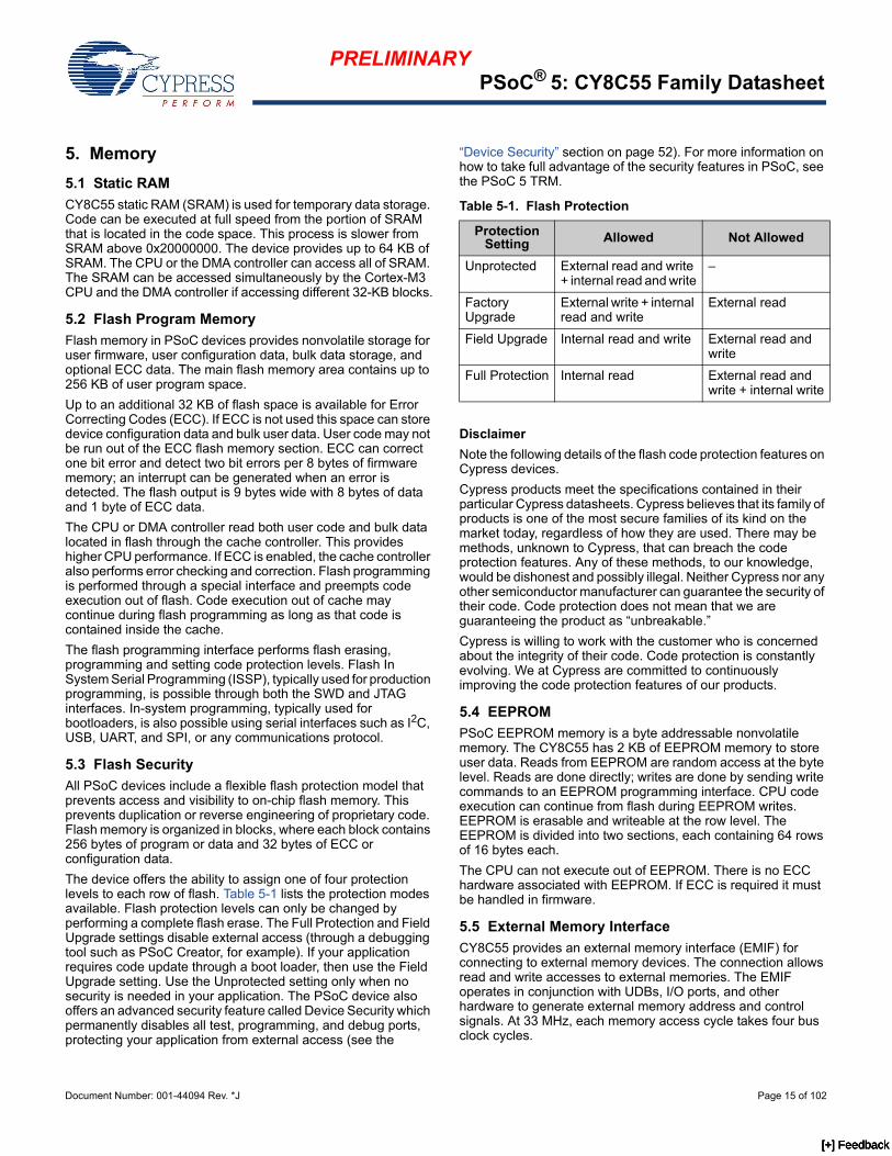
5. Memory ........................................................................ 155.1 Static RAM .......................................................... 155.2 Flash Program Memory ....................................... 155.3 Flash Security ...................................................... 155.4 EEPROM ............................................................. 155.5 External Memory Interface .................................. 155.6 Memory Map .......................................................16
6. System Integration ..................................................... 176.1 Clocking System .................................................. 176.2 Power System ..................................................... 206.3 Reset ................................................................... 246.4 I/O System and Routing ...................................... 25
7. Digital Subsystem ...................................................... 317.1 Example Peripherals ........................................... 317.2 Universal Digital Block ......................................... 347.3 UDB Array Description ........................................ 377.4 DSI Routing Interface Description ....................... 377.5 CAN .....................................................................397.6 USB .....................................................................407.7 Timers, Counters, and PWMs ............................. 407.8 I2C ....................................................................... 417.9 Digital Filter Block ................................................ 41
8. Analog Subsystem ..................................................... 428.1 Analog Routing .................................................... 428.2 Delta-sigma ADC ................................................. 448.3 Successive Approximation ADC .......................... 458.4 Comparators ........................................................ 458.5 Opamps ............................................................... 478.6 Programmable SC/CT Blocks ............................. 47
8.7 LCD Direct Drive ................................................. 488.8 CapSense ............................................................ 498.9 Temp Sensor ....................................................... 498.10 DAC ................................................................... 498.11 Up/Down Mixer .................................................. 508.12 Sample and Hold ............................................... 50
9. Programming, Debug Interfaces, Resources ........... 509.1 JTAG Interface .................................................... 519.2 SWD Interface ..................................................... 519.3 Debug Features ................................................... 519.4 Trace Features .................................................... 519.5 SWV and TRACEPORT Interfaces ..................... 529.6 Programming Features ........................................ 529.7 Device Security ................................................... 52
10. Development Support .............................................. 5210.1 Documentation .................................................. 5210.2 Online ................................................................ 5310.3 Tools .................................................................. 53
11. Electrical Specifications .......................................... 5411.1 Absolute Maximum Ratings ............................... 5411.2 Device Level Specifications ............................... 5511.3 Power Regulators .............................................. 5711.4 Inputs and Outputs ............................................ 5811.5 Analog Peripherals ............................................ 6311.6 Digital Peripherals ............................................. 7711.7 Memory ............................................................. 8111.8 PSoC System Resources .................................. 8611.9 Clocking ............................................................. 88
12. Ordering Information ................................................ 9112.1 Part Numbering Conventions ............................ 93
13. Packaging .................................................................. 9414. Acronyms .................................................................. 9615. Reference Documents .............................................. 9716. Document Conventions ........................................... 98
16.1 Units of Measure ............................................... 9817. Revision History ....................................................... 9918. Sales, Solutions, and Legal Information .............. 102
[+] Feedback [+] Feedback [+] Feedback [+] Feedback

PRELIMINARYPSoC® 5: CY8C55 Family Datasheet
Document Number: 001-44094 Rev. *J Page 3 of 102
1. Architectural Overview
Introducing the CY8C55 family of ultra low power, flash Programmable System-on-Chip (PSoC) devices, part of a scalable 8-bit PSoC 3 and 32-bit PSoC 5 platform. The CY8C55 family provides configurable blocks of analog, digital, and interconnect circuitry around a CPU subsystem. The combination of a CPU with a flexible analog subsystem, digital subsystem, routing, and I/O enables a high level of integration in a wide variety of consumer, industrial, and medical applications.
Figure 1-1. Simplified Block Diagram
DigitalFilterBlock
LCD Direct Drive
CapSense
Temperature Sensor
4 x Opamp
+
-
ADCs
4 x DAC 1 x Del Sig ADC
4 x SC/ CT Blocks (TIA, PGA, Mixer etc)
4 x CMP
+
-
Program
Debug & Trace
Boundary Scan
Program & Debug
8051 orCortex M3 CPU
Interrupt Controller
PHUBDMA
Cache Controller
SRAM
FLASH
EEPROM
EMIF
Digital Interconnect
Analog Interconnect
1.71
to5.
5V
0. 5 to 5.5 V( Optional)
4- 33 MHz( Optional)
XtalOsc
32.768 KHz( Optional)
RTC Timer
IMO Clo
ck T
ree
WDT and
Wake
ILO
Clocking System
1.8 V LDO
SMP
POR andLVD
SleepPower
Power Management System
USB PHY
3 per Opamp
GP
IOs
GP
IOs
GP
IOs
GP
IOs
GP
IOs
GP
IOs
SIO
GP
IOs
SIO
s
2 x SARADC
CAN2.0
I2CMaster/Slave
Universal Digital Block Array (24 x UDB)
4 xTimer
Counter PWM
FS USB 2.0
UDB
UDB
UDB
UDB
UDB
UDB
UDB UDB UDB
UDB
UDB
UDBUDBUDB UDB
UART
Logic
12- Bit PWM
I 2C Slave8- Bit SPI
12- Bit SPILogic
8- Bit Timer
16- Bit PRS
UDB
8- Bit Timer
Quadrature Decoder 16- Bit PWM
Se
qu
en
cer
Usa
ge
Exa
mp
le fo
r U
DB UDBUDB
UDBUDB
UDBUDB
UDBUDB
22
Memory System CPU System
Analog System
System Bus
Digital SystemSystem Wide Resources
[+] Feedback [+] Feedback [+] Feedback [+] Feedback
PRELIMINARYPSoC® 5: CY8C55 Family Datasheet
Document Number: 001-44094 Rev. *J Page 4 of 102
Figure 1-1 illustrates the major components of the CY8C55 family. They are:
■ ARM Cortex-M3 CPU subsystem
■ Nonvolatile subsystem
■ Programming, debug, and test subsystem
■ Inputs and outputs
■ Clocking
■ Power
■ Digital subsystem
■ Analog subsystem
PSoC’s digital subsystem provides half of its unique configurability. It connects a digital signal from any peripheral to any pin through the digital system interconnect (DSI). It also provides functional flexibility through an array of small, fast, low power UDBs. PSoC Creator provides a library of pre-built and tested standard digital peripherals (UART, SPI, LIN, PRS, CRC, timer, counter, PWM, AND, OR, and so on) that are mapped to the UDB array. The designer can also easily create a digital circuit using boolean primitives by means of graphical design entry. Each UDB contains programmable array logic (PAL)/programmable logic device (PLD) functionality, together with a small state machine engine to support a wide variety of peripherals.
In addition to the flexibility of the UDB array, PSoC also provides configurable digital blocks targeted at specific functions. For the CY8C55 family, these blocks can include four 16-bit timers, counters, and PWM blocks; I2C slave, master, and multimaster; Full-Speed USB; and Full CAN 2.0b.
For more details on the peripherals see the “Example Peripherals” section on page 31 of this datasheet. For information on UDBs, DSI, and other digital blocks, see the “Digital Subsystem” section on page 31 of this datasheet.
PSoC’s analog subsystem is the second half of its unique configurability. All analog performance is based on a highly accurate absolute voltage reference with less than 0.1% error over temperature and voltage. The configurable analog subsystem includes:
■ Analog muxes
■ Comparators
■ Analog mixers
■ Voltage references
■ ADCs
■ DACs
■ Digital filter block (DFB)
All GPIO pins can route analog signals into and out of the device using the internal analog bus. This allows the device to interface up to 62 discrete analog signals. One of the ADCs in the analog
subsystem is a fast, accurate, configurable delta-sigma ADC with these features:
■ Less than 100-µV offset
■ A gain error of 0.2%
■ Integral non linearity (INL) less than ±2 LSB
■ Differential non linearity (DNL) less than ±1 LSB
■ SNR better than 89 dB in 16-bit mode
This converter addresses a wide variety of precision analog applications including some of the most demanding sensors.
The CY8C55 family also offers up to two SAR ADCs. Featuring 12-bit conversions at up to 1 M samples per second, they also offer low nonlinearity and offset errors and SNR better than 70 dB. They are well-suited for a variety of higher speed analog applications.
The output of any of the ADCs can optionally feed the programmable DFB via DMA without CPU intervention. The designer can configure the DFB to perform IIR and FIR digital filters and several user defined custom functions. The DFB can implement filters with up to 64 taps. It can perform a 48-bit multiply-accumulate (MAC) operation in one clock cycle.
Four high-speed voltage or current DACs support 8-bit output signals at an update rate of up to 8 Msps. They can be routed out of any GPIO pin. You can create higher resolution voltage DAC outputs using the UDB array. This can be used to create a pulse width modulated (PWM) DAC of up to 10 bits, at up to 48 kHz. The digital DACs in each UDB support PWM, PRS, or delta-sigma algorithms with programmable widths.
In addition to the ADCs, DACs, and DFB, the analog subsystem provides multiple:
■ Comparators
■ Uncommitted opamps
■ Configurable switched capacitor/continuous time (SC/CT) blocks. These support: ❐ Transimpedance amplifiers ❐ Programmable gain amplifiers❐ Mixers❐ Other similar analog components
See the “Analog Subsystem” section on page 42 of this datasheet for more details.
PSoC’s CPU subsystem is built around a 32-bit three-stage pipelined ARM Cortex-M3 processor running at up to 80 MHz. The Cortex-M3 includes a tightly integrated nested vectored interrupt controller (NVIC) and various debug and trace modules. The overall CPU subsystem includes a DMA controller, flash cache, and RAM. The NVIC provides low latency, nested interrupts, and tail-chaining of interrupts and other features to increase the efficiency of interrupt handling. The DMA controller enables peripherals to exchange data without CPU involvement. This allows the CPU to run slower (saving power) or use those CPU cycles to improve the performance of firmware algorithms. The flash cache also reduces system power consumption by allowing less frequent flash access.
[+] Feedback [+] Feedback [+] Feedback [+] Feedback

PRELIMINARYPSoC® 5: CY8C55 Family Datasheet
Document Number: 001-44094 Rev. *J Page 5 of 102
PSoC’s nonvolatile subsystem consists of flash, byte-writeable EEPROM, and nonvolatile configuration options. It provides up to 256 KB of on-chip flash. The CPU can reprogram individual blocks of flash, enabling boot loaders. The designer can enable an ECC for high reliability applications. A powerful and flexible protection model secures the user's sensitive information, allowing selective memory block locking for read and write protection. Two KB of byte-writable EEPROM is available on-chip to store application data. Additionally, selected configuration options such as boot speed and pin drive mode are stored in nonvolatile memory. This allows settings to activate immediately after POR.
The three types of PSoC I/O are extremely flexible. All I/Os have many drive modes that are set at POR. PSoC also provides up to four I/O voltage domains through the VDDIO pins. Every GPIO has analog I/O, LCD drive, flexible interrupt generation, slew rate control, and digital I/O capability. The SIOs on PSoC allow VOH to be set independently of VDDIO when used as outputs. When SIOs are in input mode they are high impedance. This is true even when the device is not powered or when the pin voltage goes above the supply voltage. This makes the SIO ideally suited for use on an I2C bus where the PSoC may not be powered when other devices on the bus are. The SIO pins also have high current sink capability for applications such as LED drives. The programmable input threshold feature of the SIO can be used to make the SIO function as a general purpose analog comparator. For devices with FS USB, the USB physical interface is also provided (USBIO). When not using USB, these pins may also be used for limited digital functionality and device programming. All the features of the PSoC I/Os are covered in detail in the “I/O System and Routing” section on page 25 of this datasheet.
The PSoC device incorporates flexible internal clock generators, designed for high stability and factory trimmed for high accuracy. The Internal Main Oscillator (IMO) is the master clock base for the system, and has one-percent accuracy at 3 MHz. The IMO can be configured to run from 3 MHz up to 74 MHz. Multiple clock derivatives can be generated from the main clock frequency to meet application needs. The device provides a PLL to generate system clock frequencies up to 80 MHz from the IMO, external crystal, or external reference clock. It also contains a separate, very low-power ILO for the sleep and watchdog timers. A 32.768-kHz external watch crystal is also supported for use in RTC applications. The clocks, together with programmable clock dividers, provide the flexibility to integrate most timing requirements.
The CY8C55 family supports a wide supply operating range from 1.71 to 5.5 V. This allows operation from regulated supplies such as 1.8 ± 5%, 2.5 V ±10%, 3.3 V ± 10%, or 5.0 V ± 10%, or directly from a wide range of battery types. In addition, it provides an integrated high efficiency synchronous boost converter that can power the device from supply voltages as low as 0.5 V. This enables the device to be powered directly from a single battery or solar cell. In addition, the designer can use the boost converter to generate other voltages required by the device, such as a 3.3 V supply for LCD glass drive. The boost’s output is available on the VBOOST pin, allowing other devices in the application to be powered from the PSoC.
PSoC supports a wide range of low power modes. These include a 300-nA hibernate mode with RAM retention and a 2-µA sleep mode with RTC. In the second mode, the optional 32.768-kHz watch crystal runs continuously and maintains an accurate RTC.
Power to all major functional blocks, including the programmable digital and analog peripherals, can be controlled independently by firmware. This allows low power background processing when some peripherals are not in use. This, in turn, provides a total device current of only 2 mA when the CPU is running at 6 MHz.
The details of the PSoC power modes are covered in the “Power System” section on page 20 of this datasheet.
PSoC uses JTAG (4 wire) or SWD (2 wire) interfaces for programming, debug, and test. Using these standard interfaces enables the designer to debug or program the PSoC with a variety of hardware solutions from Cypress or third party vendors. The Cortex-M3 debug and trace modules include FPB, DWT, ETM, and ITM. These modules have many features to help solve difficult debug and trace problems. Details of the programming, test, and debugging interfaces are discussed in the “Programming, Debug Interfaces, Resources” section on page 50 of this datasheet.
2. Pinouts
The VDDIO pin that supplies a particular set of pins is indicated by the black lines drawn on the pinout diagrams in Figure 2-2 and Figure 2-3. Using the VDDIO pins, a single PSoC can support multiple interface voltage levels, eliminating the need for off-chip level shifters. Each VDDIO may sink up to 100 mA total to its associated I/O pins and opamps. On the 68-pin and 100-pin devices, each set of VDDIO associated pins may sink up to 100 mA. The 48 pin device may sink up to 100 mA total for all Vddio0 plus Vddio2 associated I/O pins and 100 mA total for all Vddio1 plus Vddio3 associated I/O pins.
[+] Feedback [+] Feedback [+] Feedback [+] Feedback

PRELIMINARYPSoC® 5: CY8C55 Family Datasheet
Document Number: 001-44094 Rev. *J Page 6 of 102
Figure 2-1. 48-pin SSOP Part Pinout[3]
Figure 2-2. 68-pin QFN Part Pinout[4]
SSOP
Vssa(SIO) P12[3] 2 47Vcca(OpAmp2out, GPIO) P0[0] 3 46P15[3] (GPIO, kHz XTAL: Xi)(OpAmp0out, GPIO) P0[1] 4 45
P12[0] (SIO, I2C1: SCL)Vddio0 7 42
P12[1] (SIO, I2C1: SDA)6 43(OpAmp0-/Extref0, GPIO) P0[3]
P15[1] (GPIO, MHz XTAL: Xi)(OpAmp2-, GPIO) P0[5] 9 40P15[0] (GPIO, MHz XTAL: Xo)(IDAC0, GPIO) P0[6] 10 39Vccd(IDAC2, GPIO) P0[7] 11 38VssdVccd 12 37VdddVssd 13 36P15[7] (USBIO, D-, SWDCK)Vddd 14 35P15[6] (USBIO, D+, SWDIO)(TRACECLK, GPIO) P2[3] 15 34P1[7] (GPIO)(TRACEDATA[0], GPIO) P2[4] 16 33P1[6] (GPIO)Vddio2 17 32Vddio1(TRACEDATA[1], GPIO) P2[5] 18 31P1[5] (GPIO, nTRST)(TRACEDATA[2], GPIO) P2[6] 19 30P1[4] (GPIO, TDI)(TRACEDATA[3], GPIO) P2[7] 20 29P1[3] (GPIO, TDO, SWV)Vssb 21 28
Ind 22 27P1[1] (GPIO, TCK, SWDCK)Vboost 23 26P1[0] (GPIO, TMS, SWDIO)Vbat 24 25
Vdda(SIO) P12[2] 1 48
Vddio3(OpAmp2+, GPIO) P0[4] 8 41
P15[2] (GPIO, kHz XTAL: Xo)(OpAmp0+, GPIO) P0[2] 5 44
Lines show Vddio to I/O supply association
P1[2] (GPIO, configurable XRES)
(TRACEDATA[2], GPIO) P2[6](TRACEDATA[3], GPIO) P2[7]
(I2C0: SCL, SIO) P12[4]
(I2C0: SDA, SIO) P12[5]
VssbInd
VboostVbatVssd
XRES(TMS, SWDIO, GPIO) P1[0](TCK, SWDCK, GPIO) P1[1]
(configurable XRES, GPIO) P1[2]
(TDO, SWV, GPIO) P1[3](TDI, GPIO) P1[4]
(nTRST, GPIO) P1[5]Vddio1
(GP
IO)
P1[
6]
Vcc
d
(OpA
mp3
+, G
PIO
) P
3[3]
(GP
IO)
P1[
7](S
IO)
P1
2[6]
(SIO
) P
12[
7]
(US
BIO
, D+
, SW
DIO
) P
15[
6](U
SB
IO, D
-, S
WD
CK
) P
15[
7]
Vdd
d
Vss
d
(MH
z X
TA
L: X
o, G
PIO
) P
15[
0]
(MH
z X
TA
L: X
i, G
PIO
) P
15[
1](I
DA
C1,
GP
IO)
P3[
0](I
DA
C3,
GP
IO)
P3[
1](O
pA
mp3
-/E
xtre
f1, G
PIO
) P
3[2]
(OpA
mp1
-, G
PIO
) P
3[4]
(OpA
mp1
+, G
PIO
) P
3[5]
P0[3] (GPIO, OpAmp0-/Extref0)
P0[2] (GPIO, OpAmp0+)
P0[1] (GPIO, OpAmp0out)
P0[0] (GPIO, OpAmp2out)
P12[3] (SIO)P12[2] (SIO)
Vssd VddaVssaVcca
P15[3] (GPIO, kHz XTAL: Xi)P15[2] (GPIO, kHz XTAL: Xo)
P12[1] (SIO, I2C1: SDA)
P12[0] (SIO, 12C1: SCL)
P3[7] (GPIO, OpAmp3out)P3[6] (GPIO, OpAmp1out)Vddio3
P2[
5] (
GP
IO, T
RA
CE
DA
TA
[1])
Vdd
io2
P2[
4] (
GP
IO, T
RA
CE
DA
TA
[0])
P2[
3] (
GP
IO, T
RA
CE
CLK
)
P2[
2] (
GP
IO)
P2[
1] (
GP
IO)
P2[
0] (
GP
IO)
P15
[5] (
GP
OI)
P15
[4] (
GP
IO)
Vdd
d
Vss
dV
ccd
P0[
7] (
GP
IO, I
DA
C2)
P0[
6] (
GP
IO, I
DA
C0)
P0[
5] (
GP
IO, O
pAm
p2-)
P0[
4] (
GP
IO, O
pAm
p2+
)V
ddio
0
5150
494847
46
45
444342
41
4039
383736
35
68 67 66 65 64 63 62 61 60 59 58 57 56 55 54 53 52
10
1112131415
16
17
12
3
4
56
789
18 19 20 21 22 23 24 25 26 27 28 29 30 31 32 33 34
QFN(Top View)
Lines show Vddio to I/O supply association
[3]
[4]
Notes3. Pins are No Connect (NC) on devices without USB. NC means that the pin has no electrical connection. The pin can be left floating or tied to a supply voltage or ground.4. The center pad on the QFN package should be connected to digital ground (VSSD) for best mechanical, thermal, and electrical performance. If not connected to
ground, it should be electrically floated and not connected to any other signal.
[+] Feedback [+] Feedback [+] Feedback [+] Feedback
PRELIMINARYPSoC® 5: CY8C55 Family Datasheet
Document Number: 001-44094 Rev. *J Page 7 of 102
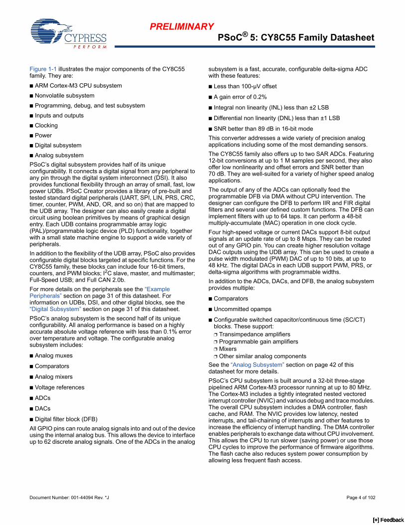
Figure 2-3. 100-pin TQFP Part Pinout
Figure 2-4 and Figure 2-5 on page 8 show an example schematic and an example PCB layout, for the 100-pin TQFP part, for optimal analog performance on a two-layer board.
■ The two pins labeled VDDD must be connected together.
■ The two pins labeled VCCD must be connected together, with capacitance added, as shown in Figure 2-4 and Power System on page 20. The trace between the two VCCD pins should be as short as possible.
■ The two pins labeled VSSD must be connected together.
TQFP
(TRACEDATA[1], GPIO) P2[5](TRACEDATA[2], GPIO) P2[6](TRACEDATA[3], GPIO) P2[7]
(I2C0: SCL, SIO) P12[4]
(I2C0: SDA, SIO) P12[5](GPIO) P6[4]
(GPIO) P6[5](GPIO) P6[6]
(GPIO) P6[7]
VssbInd
Vboost
Vbat
VssdXRES
(GPIO) P5[0](GPIO) P5[1]
(GPIO) P5[2]
(GPIO) P5[3](TMS, SWDIO, GPIO) P1[0]
(TCK, SWDCK, GPIO) P1[1]
(configurable XRES, GPIO) P1[2](TDO, SWV, GPIO) P1[3]
(TDI, GPIO) P1[4](nTRST, GPIO) P1[5]
Vdd
io1
(GP
IO)
P5
[7]
NC
(OpA
mp3
-/E
xtre
f1, G
PIO
) P
3[2]
(GP
IO)
P1
[6]
(GP
IO)
P1
[7]
(SIO
) P
12[6
]
(SIO
) P
12[7
](G
PIO
) P
5[4
]
(GP
IO)
P5
[5]
(GP
IO)
P5
[6]
(US
BIO
, D+
, SW
DIO
) P
15[6
]
(US
BIO
, D-,
SW
DC
K)
P15
[7]
Vdd
dV
ssd
Vcc
d
NC
(MH
z X
TA
L: X
o, G
PIO
) P
15[0
]
(MH
z X
TA
L: X
i, G
PIO
) P
15[1
]
(ID
AC
1, G
PIO
) P
3[0]
(ID
AC
3, G
PIO
) P
3[1]
(OpA
mp3
+, G
PIO
) P
3[3]
(OpA
mp1
-, G
PIO
) P
3[4]
(OpA
mp1
+, G
PIO
) P
3[5]
Vdd
io3
Vddio0
P0[3] (GPIO, OpAmp0-/Extref0)
P0[2] (GPIO, OpAmp0+)
P0[1] (GPIO, OpAmp0out)
P0[0] (GPIO, OpAmp2out)P4[1] (GPIO)
P4[0] (GPIO)P12[3] (SIO)P12[2] (SIO)Vssd
VddaVssa
Vcca
NC
NCNCNCNCNCP15[3] (GPIO, kHz XTAL: Xi)P15[2] (GPIO, kHz XTAL: Xo)
P12[1] (SIO, I2C1: SDA)P12[0] (SIO, I2C1: SCL)
P3[7] (GPIO, OpAmp3out)
P3[6] (GPIO, OpAmp1out)
Vdd
io2
P2[
4] (
GP
IO, T
RA
CE
DA
TA
[0])
P2[
3] (
GP
IO, T
RA
CE
CLK
)P
2[2]
(G
PIO
)
P2[
1] (
GP
IO)
P2[
0] (
GP
IO)
P15
[5] (
GP
IO)
P15
[4] (
GP
IO)
P6[
3] (
GP
IO)
P6[
2] (
GP
IO)
P6[
1] (
GP
IO)
P6[
0] (
GP
IO)
Vdd
d
Vss
d
Vcc
dP
4[7]
(G
PIO
)P
4[6]
(G
PIO
)
P4[
5] (
GP
IO)
P4[
4] (
GP
IO)
P4[
3] (
GP
IO)
P4[
2] (
GP
IO)
P0[
7] (
GP
IO, I
DA
C2)
P0[
6] (
GP
IO, I
DA
C0)
P0[
5] (
GP
IO, O
pAm
p2-)
P0[
4] (
GP
IO, O
pAm
p2+
)
7574
737271
70
69
686766
65
6463
626160
5958575655
54535251
100
99 98 97 96 95 94 93 92 91 90 89 88 87 86 85 84 83 82 81 80 79 78 77 76
10
1112131415
16
17
1819202122
23
2425
12
3
4
56
789
26 27 28 29 30 31 32 33 34 35 36 37 38 39 40 41 42 43 44 45 46 47 48 5049
Lines show Vddio to I/O supply association
[5]
[6]
Notes5. Pins are No Connect (NC) on devices without USB. NC means that the pin has no electrical connection. The pin can be left floating or tied to a supply voltage or ground.6. The center pad on the QFN package should be connected to digital ground (VSSD) for best mechanical, thermal, and electrical performance. If not connected to ground,
it should be electrically floated and not connected to any other signal.
[+] Feedback [+] Feedback [+] Feedback [+] Feedback

PRELIMINARYPSoC® 5: CY8C55 Family Datasheet
Document Number: 001-44094 Rev. *J Page 8 of 102
Figure 2-4. Example Schematic for 100-pin TQFP Part with Power Connections
Note The two VCCD pins must be connected together with as short a trace as possible. A trace under the device is recommended, as shown in Figure 2-5.
Figure 2-5. Example PCB Layout for 100-pin TQFP Part for Optimal Analog Performance
Vssb10
Ind11
Vboost12
Vbat13
Vssd14
XRES15V
dd
d3
7
Vss
d3
8
Vcc
d3
9
Vcca 63Vssa 64Vdda 65Vssd 66
Vcc
d8
6V
ssd
87
Vd
dd
88
SIO, P12[2] 67SIO, P12[3] 68
P4[0] 69P4[1] 70
OA2out, P0[0] 71OA0out, P0[1] 72
OA0+, P0[2] 73OA0-, REF0, P0[3] 74
Vddio0 75OA
2+
, P0
[4]
76
OA
2-,
P0
[5]
77
IDA
C0
, P
0[6
]7
8ID
AC
2,
P0
[7]
79
P4
[2]
80
P4
[3]
81
P4
[4]
82
P4
[5]
83
P4
[6]
84
P4
[7]
85
P5[0]16
P5[1]17
P5[2]18
P5[3]19
P1[0], SWIO, TMS20
P1[1], SWDIO, TCK21
P1[2]22
P1[3], SWV, TDO23
P1[4], TDI24
P1[5], nTRST25
Vd
dio
12
6
P1
[6]
27
P1
[7]
28
P1
2[6
], S
IO2
9
P1
2[7
], S
IO3
0
P5
[4]
31
P5
[5]
32
P5
[6]
33
P5
[7]
34
US
B D
+,
P1
5[6
]3
5
US
B D
-, P
15
[7]
36
P6[7]9
P6
[0]
89
P6
[1]
90
P6
[2]
91
P6
[3]
92
P1
5[4
]9
3P
15
[5]
94
P2
[0]
95
P2
[1]
96
P2
[2]
97
P2
[3]
98
P2
[4]
99
Vd
dio
21
00
P2[5]1
P2[6]2
P2[7]3
P12[4], SIO4
P12[5], SIO5
P6[4]6
P6[5]7
P6[6]8
NC
40
NC
41
P1
5[0
], M
HzX
ou
t4
2
P1
5[1
], M
HzX
in4
3
P3
[0],
IDA
C1
44
P3
[1],
IDA
C3
45
P3
[2],
OA
3-,
RE
F1
46
P3
[3],
OA
3+4
7
P3
[4],
OA
1-4
8
P3
[5],
OA
1+4
9
Vd
dio
35
0
OA1out, P3[6] 51OA3out, P3[7] 52
SIO, P12[0] 53SIO, P12[1] 54
kHzXout, P15[2] 55kHzXin, P15[3] 56
NC 57NC 58NC 59NC 60NC 61NC 62
U2CY8C55xx
VssdVdda
Vcca
Vcc
d
Vss
d
Vd
dd
Vssd
Vd
dd
Vdd
dV
ssd
P3
2
Vssa
Vssa
Vssd
VssdVssd
Vssd
0.1 uFC8
Vssd
Vddd
Vddd Vddd
Vddd
Vssa Vssa
Vddd
Vssd
1 uFC9
0.1 uFC10
0.1 uFC11
0.1 uFC14
0.1 uFC16
0.1 uFC12
0.1 uFC6
0.1 uFC2
1 uFC15
1 uFC1
Vssd
Vddd
Vssd
VddaVssd
Vccd
10 uF, 6.3 V
C13
1 uFC17
Vssa
Vdda
Vddd Vssd Vdda
Vssa
VssdPlane
VssaPlane
[+] Feedback [+] Feedback [+] Feedback [+] Feedback
PRELIMINARYPSoC® 5: CY8C55 Family Datasheet
Document Number: 001-44094 Rev. *J Page 9 of 102
3. Pin Descriptions
IDAC0, IDAC1, IDAC2, IDAC3. Low-resistance output pin for high-current DACs (IDAC).
OpAmp0out, OpAmp1out, OpAmp2out, OpAmp3out. High current output of uncommitted opamp.[7]
Extref0, Extref1. External reference input to the analog system.
OpAmp0-, OpAmp1-, OpAmp2-, OpAmp3-. Inverting input to uncommitted opamp.
OpAmp0+, OpAmp1+, OpAmp2+, OpAmp3+. Noninverting input to uncommitted opamp.
GPIO. Provides interfaces to the CPU, digital peripherals, analog peripherals, interrupts, LCD segment drive, and CapSense.[7]
I2C0: SCL, I2C1: SCL. I2C SCL line providing wake from sleep on an address match. Any I/O pin can be used for I2C SCL if wake from sleep is not required.
I2C0: SDA, I2C1: SDA. I2C SDA line providing wake from sleep on an address match. Any I/O pin can be used for I2C SDA if wake from sleep is not required.
Ind. Inductor connection to boost pump.
kHz XTAL: Xo, kHz XTAL: Xi. 32.768-kHz crystal oscillator pin.
MHz XTAL: Xo, MHz XTAL: Xi. 4 to 33-MHz crystal oscillator pin.
nTRST. Optional JTAG Test Reset programming and debug port connection to reset the JTAG connection.
SIO. Provides interfaces to the CPU, digital peripherals and interrupts with a programmable high threshold voltage, analog comparator, high sink current, and high impedance state when the device is unpowered.
SWDCK. SWD Clock programming and debug port connection.
SWDIO. SWD Input and Output programming and debug port connection.
TCK. JTAG Test Clock programming and debug port connection.
TDI. JTAG Test Data In programming and debug port connection.
TDO. JTAG Test Data Out programming and debug port connection.
TMS. JTAG Test Mode Select programming and debug port connection.
TRACECLK. Cortex-M3 TRACEPORT connection, clocks TRACEDATA pins.
TRACEDATA[3:0]. Cortex-M3 TRACEPORT connections, output data.
SWV. SWV output.
USBIO, D+. Provides D+ connection directly to a USB 2.0 bus. May be used as a digital I/O pin; it is powered from VDDD instead of from a VDDIO. Pins are No Connect (NC) on devices without USB.[8]
USBIO, D-. Provides D- connection directly to a USB 2.0 bus. May be used as a digital I/O pin; it is powered from VDDD instead of from a VDDIO. Pins are No Connect (NC) on devices without USB.[8]
VBOOST. Power sense connection to boost pump.
VBAT. Battery supply to boost pump.
VCCA. Output of analog core regulator and input to analog core. Requires a 1 µF capacitor to VSSA. Regulator output not for external use.
VCCD. Output of digital core regulator and input to digital core. The two VCCD pins must be shorted together, with the trace between them as short as possible, and a 1 µF capacitor to VSSD; see Power System on page 20. Regulator output not for external use.
VDDA. Supply for all analog peripherals and analog core regulator. VDDA must be the highest voltage present on the device. All other supply pins must be less than or equal to VDDA.
VDDD. Supply for all digital peripherals and digital core regulator. VDDD must be less than or equal to VDDA.
VSSA. Ground for all analog peripherals.
VSSB. Ground connection for boost pump.
VSSD. Ground for all digital logic and I/O pins.
VDDIO0, VDDIO1, VDDIO2, VDDIO3. Supply for I/O pins. Each VDDIO must be tied to a valid operating voltage (1.71 V to 5.5 V), and must be less than or equal to VDDA. If the I/O pins associated with VDDIO0, VDDIO2 or VDDIO3 are not used then that VDDIO should be tied to ground (VSSD or VSSA).
XRES (and configurable XRES). External reset pin. Active low with internal pull-up. In 48-pin SSOP parts, P1[2] may be configured as XRES. In all other parts the pin is configured as a GPIO.
4. CPU
4.1 ARM Cortex-M3 CPU
The CY8C55 family of devices has an ARM Cortex-M3 CPU core. The Cortex-M3 is a low-power 32-bit three-stage pipelined Harvard-architecture CPU that delivers 1.25 DMIPS/MHz. It is intended for deeply embedded applications that require fast interrupt handling features.
Notes7. GPIOs with opamp outputs are not recommended for use with CapSense.8. Pins are No Connect (NC) on devices without USB. NC means that the pin has no electrical connection. The pin can be left floating or tied to a supply voltage or ground.
[+] Feedback [+] Feedback [+] Feedback [+] Feedback

PRELIMINARYPSoC® 5: CY8C55 Family Datasheet
Document Number: 001-44094 Rev. *J Page 10 of 102
Figure 4-1. ARM Cortex-M3 Block Diagram
The Cortex-M3 CPU subsystem includes these features:
■ ARM Cortex-M3 CPU
■ Programmable nested vectored interrupt controller (NVIC), tightly integrated with the CPU core
■ Full featured debug and trace modules, tightly integrated with the CPU core
■ Up to 256 KB of flash memory, 2 KB of EEPROM, and 64 KB of SRAM
■ Cache controller
■ Peripheral HUB (PHUB)
■ DMA controller
■ External memory interface (EMIF)
4.0.1 Cortex-M3 Features
The Cortex-M3 CPU features include:
■ 4 GB address space. Predefined address regions for code, data, and peripherals. Multiple buses for efficient and simultaneous accesses of instructions, data, and peripherals.
■ The Thumb®-2 instruction set, which offers ARM-level performance at Thumb-level code density. This includes 16-bit and 32-bit instructions. Advanced instructions include:❐ Bit-field control❐ Hardware multiply and divide❐ Saturation❐ If-Then❐ Wait for events and interrupts❐ Exclusive access and barrier❐ Special register access
The Cortex-M3 does not support ARM instructions.
■ Bit-band support. Atomic bit-level write and read operations.
■ Unaligned data storage and access. Contiguous storage of data of different byte lengths.
Nested Vectored Interrupt
Controller (NVIC)
Debug Block (Serial and
JTAG)
Embedded Trace Module
(ETM)
Trace Port Interface Unit
(TPIU)
Interrupt Inputs
JTAG/SWDTrace Pins:5 for TRACEPORT or1 for SWV mode
Cortex M3 CPU Core
I-Bus S-BusD-Bus
256 KB ECC Flash
Cache
32 KB SRAM
DMA AHB Bridge & Bus Matrix
PHUB
GPIO & EMIF
Prog. Digital
Prog. Analog
Special Functions
Peripherals
AHB Spokes
AHB AHB
AHB
Bus Matrix
Cortex M3 WrapperC-Bus
Data Watchpoint and
Trace (DWT)
Instrumentation Trace Module
(ITM)
Flash Patch and Breakpoint
(FPB)
Bus Matrix
32 KB SRAM
Bus Matrix
[+] Feedback [+] Feedback [+] Feedback [+] Feedback

PRELIMINARYPSoC® 5: CY8C55 Family Datasheet
Document Number: 001-44094 Rev. *J Page 11 of 102
■ Operation at two privilege levels (privileged and user) and in two modes (thread and handler). Some instructions can only be executed at the privileged level. There are also two stack pointers: Main (MSP) and Process (PSP). These features support a multitasking operating system running one or more user-level processes.
■ Extensive interrupt and system exception support.
4.0.2 Cortex-M3 Operating Modes
The Cortex-M3 operates at either the privileged level or the user level, and in either the thread mode or the handler mode. Because the handler mode is only enabled at the privileged level, there are actually only three states, as shown in Table 4-1.
At the user level, access to certain instructions, special registers, configuration registers, and debugging components is blocked. Attempts to access them cause a fault exception. At the privileged level, access to all instructions and registers is allowed.
The processor runs in the handler mode (always at the privileged level) when handling an exception, and in the thread mode when not.
4.0.3 CPU Registers
The Cortex-M3 CPU registers are listed in Table 4-2. Registers R0-R15 are all 32 bits wide.
4.1 Cache Controller
The CY8C55 family has a 1 KB instruction cache between the CPU and the flash memory. This improves instruction execution rate and reduces system power consumption by requiring less frequent flash access.
4.2 DMA and PHUB
The PHUB and the DMA controller are responsible for data transfer between the CPU and peripherals, and also data transfers between peripherals. The PHUB and DMA also control device configuration during boot. The PHUB consists of:
■ A central hub that includes the DMA controller, arbiter, and router
■ Multiple spokes that radiate outward from the hub to most peripherals
Table 4-1. Operational Level
Condition Privileged User
Running an exception Handler mode Not used
Running main program Thread mode Thread mode
Table 4-2. Cortex M3 CPU Registers
Register Description
R0-R12 General purpose registers R0-R12 have no special architecturally defined uses. Most instructions that specify a general purpose register specify R0-R12.
■ Low registers: Registers R0-R7 are accessible by all instructions that specify a general purpose register.
■ High registers: Registers R8-R12 are accessible by all 32-bit instructions that specify a general purpose register; they are not accessible by all 16-bit instructions.
R13 R13 is the stack pointer register. It is a banked register that switches between two 32-bit stack pointers: the main stack pointer (MSP) and the process stack pointer (PSP). The PSP is used only when the CPU operates at the user level in thread mode. The MSP is used in all other privilege levels and modes. Bits[0:1] of the SP are ignored and considered to be 0, so the SP is always aligned to a word (4 byte) boundary.
R14 R14 is the link register (LR). The LR stores the return address when a subroutine is called.
R15 R15 is the program counter (PC). Bit 0 of the PC is ignored and considered to be 0, so instructions are always aligned to a half word (2 byte) boundary.
xPSR The program status registers are divided into three status registers, which are accessed either together or separately:
■ Application program status register (APSR) holds program execution status bits such as zero, carry, negative, in bits[27:31].
■ Interrupt program status register (IPSR) holds the current exception number in bits[0:8].
■ Execution program status register (EPSR) holds control bits for interrupt continuable and IF-THEN instructions in bits[10:15] and [25:26]. Bit 24 is always set to 1 to indicate Thumb mode. Trying to clear it causes a fault exception.
PRIMASK A 1-bit interrupt mask register. When set, it allows only the nonmaskable interrupt (NMI) and hard fault exception. All other exceptions and interrupts are masked.
FAULTMASK A 1-bit interrupt mask register. When set, it allows only the NMI. All other exceptions and interrupts are masked.
BASEPRI A register of up to nine bits that define the masking priority level. When set, it disables all interrupts of the same or higher priority value. If set to 0 then the masking function is disabled.
CONTROL A 2-bit register for controlling the operating mode.
Bit 0: 0 = privileged level in thread mode, 1 = user level in thread mode.
Bit 1: 0 = default stack (MSP) is used, 1 = alternate stack is used. If in thread mode or user level then the alternate stack is the PSP. There is no alternate stack for handler mode; the bit must be 0 while in handler mode.
Table 4-2. Cortex M3 CPU Registers (continued)
Register Description
[+] Feedback [+] Feedback [+] Feedback [+] Feedback

PRELIMINARYPSoC® 5: CY8C55 Family Datasheet
Document Number: 001-44094 Rev. *J Page 12 of 102
There are two PHUB masters: the CPU and the DMA controller. Both masters may initiate transactions on the bus. The DMA channels can handle peripheral communication without CPU intervention. The arbiter in the central hub determines which DMA channel is the highest priority if there are multiple requests.
4.2.1 PHUB Features
■ CPU and DMA controller are both bus masters to the PHUB
■ Eight Multi-layer AHB Bus parallel access paths (spokes) for peripheral access
■ Simultaneous CPU and DMA access to peripherals located on different spokes
■ Simultaneous DMA source and destination burst transactions on different spokes
■ Supports 8-, 16-, 24-, and 32-bit addressing and data
4.2.2 DMA Features
■ 24 DMA channels
■ Each channel has one or more transaction descriptors (TDs) to configure channel behavior. Up to 128 total TDs can be defined
■ TDs can be dynamically updated
■ Eight levels of priority per channel
■ Any digitally routable signal, the CPU, or another DMA channel, can trigger a transaction
■ Each channel can generate up to two interrupts per transfer
■ Transactions can be stalled or canceled
■ Supports transaction size of infinite or 1 to 64k bytes
■ Large transactions may be broken into smaller bursts of 1 to 127 bytes
■ TDs may be nested and/or chained for complex transactions
4.2.3 Priority Levels
The CPU always has higher priority than the DMA controller when their accesses require the same bus resources. Due to the system architecture, the CPU can never starve the DMA. DMA
channels of higher priority (lower priority number) may interrupt current DMA transfers. In the case of an interrupt, the current transfer is allowed to complete its current transaction. To ensure latency limits when multiple DMA accesses are requested simultaneously, a fairness algorithm guarantees an interleaved minimum percentage of bus bandwidth for priority levels 2 through 7. Priority levels 0 and 1 do not take part in the fairness algorithm and may use 100% of the bus bandwidth. If a tie occurs on two DMA requests of the same priority level, a simple round robin method is used to evenly share the allocated bandwidth. The round robin allocation can be disabled for each DMA channel, allowing it to always be at the head of the line. Priority levels 2 to 7 are guaranteed the minimum bus bandwidth shown in Table 4-4 after the CPU and DMA priority levels 0 and 1 have satisfied their requirements.
When the fairness algorithm is disabled, DMA access is granted based solely on the priority level; no bus bandwidth guarantees are made.
4.2.4 Transaction Modes Supported
The flexible configuration of each DMA channel and the ability to chain multiple channels allow the creation of both simple and complex use cases. General use cases include, but are not limited to:
4.2.4.2 Simple DMA
In a simple DMA case, a single TD transfers data between a source and sink (peripherals or memory location).
4.2.4.3 Auto Repeat DMA
Auto repeat DMA is typically used when a static pattern is repetitively read from system memory and written to a peripheral. This is done with a single TD that chains to itself.
4.2.4.4 Ping Pong DMA
A ping pong DMA case uses double buffering to allow one buffer to be filled by one client while another client is consuming the data previously received in the other buffer. In its simplest form, this is done by chaining two TDs together so that each TD calls the opposite TD when complete.
4.2.4.5 Circular DMA
Circular DMA is similar to ping pong DMA except it contains more than two buffers. In this case there are multiple TDs; after the last TD is complete it chains back to the first TD.
Table 4-3. PHUB Spokes and Peripherals
PHUB Spokes Peripherals
0 SRAM
1 IOs, PICU, EMIF
2 PHUB local configuration, Power manager, Clocks, IC, SWV, EEPROM, Flash programming interface
3 Analog interface and trim, Decimator
4 USB, CAN, I2C, Timers, Counters, and PWMs
5 DFB
6 UDBs group 1
7 UDBs group 2
Table 4-4. Priority Levels
Priority Level % Bus Bandwidth
0 100.0
1 100.0
2 50.0
3 25.0
4 12.5
5 6.2
6 3.1
7 1.5
[+] Feedback [+] Feedback [+] Feedback [+] Feedback

PRELIMINARYPSoC® 5: CY8C55 Family Datasheet
Document Number: 001-44094 Rev. *J Page 13 of 102
4.2.4.6 Indexed DMA
In an indexed DMA case, an external master requires access to locations on the system bus as if those locations were shared memory. As an example, a peripheral may be configured as an SPI or I2C slave where an address is received by the external master. That address becomes an index or offset into the internal system bus memory space. This is accomplished with an initial “address fetch” TD that reads the target address location from the peripheral and writes that value into a subsequent TD in the chain. This modifies the TD chain on the fly. When the “address fetch” TD completes it moves on to the next TD, which has the new address information embedded in it. This TD then carries out the data transfer with the address location required by the external master.
4.2.4.7 Scatter Gather DMA
In the case of scatter gather DMA, there are multiple noncontiguous sources or destinations that are required to effectively carry out an overall DMA transaction. For example, a packet may need to be transmitted off of the device and the packet elements, including the header, payload, and trailer, exist in various noncontiguous locations in memory. Scatter gather DMA allows the segments to be concatenated together by using multiple TDs in a chain. The chain gathers the data from the multiple locations. A similar concept applies for the reception of data onto the device. Certain parts of the received data may need to be scattered to various locations in memory for software processing convenience. Each TD in the chain specifies the location for each discrete element in the chain.
4.2.4.8 Packet Queuing DMA
Packet queuing DMA is similar to scatter gather DMA but specifically refers to packet protocols. With these protocols, there may be separate configuration, data, and status phases associated with sending or receiving a packet.
For instance, to transmit a packet, a memory mapped configuration register can be written inside a peripheral, specifying the overall length of the ensuing data phase. The CPU can set up this configuration information anywhere in system memory and copy it with a simple TD to the peripheral. After the configuration phase, a data phase TD (or a series of data phase TDs) can begin (potentially using scatter gather). When the data phase TD(s) finish, a status phase TD can be invoked that reads some memory mapped status information from the peripheral and copies it to a location in system memory specified by the CPU for later inspection. Multiple sets of configuration, data, and status phase “subchains” can be strung together to create larger chains that transmit multiple packets in this way. A similar concept exists in the opposite direction to receive the packets.
4.2.4.9 Nested DMA
One TD may modify another TD, as the TD configuration space is memory mapped similar to any other peripheral. For example, a first TD loads a second TD’s configuration and then calls the second TD. The second TD moves data as required by the application. When complete, the second TD calls the first TD, which again updates the second TD’s configuration. This process repeats as often as necessary.
4.3 Interrupt Controller
The Cortex-M3 NVIC supports 16 system exceptions and 32 interrupts from peripherals, as shown in Table 4-5.
Table 4-5. Cortex-M3 Exceptions and Interrupts
Exception Number Exception Type Priority Exception Table
Address Offset Function
0x00 Starting value of R13 / MSP
1 Reset -3 (highest) 0x04 Reset
2 NMI -2 0x08 Non maskable interrupt
3 Hard fault -1 0x0C All classes of fault, when the corresponding fault handler cannot be activated because it is currently disabled or masked
4 MemManage Programmable 0x10 Memory management fault, for example, instruction fetch from a nonexecutable region
5 Bus fault Programmable 0x14 Error response received from the bus system; caused by an instruction prefetch abort or data access error
6 Usage fault Programmable 0x18 Typically caused by invalid instructions or trying to switch to ARM mode
7 – 10 - - 0x1C – 0x28 Reserved
11 SVC Programmable 0x2C System service call via SVC instruction
12 Debug monitor Programmable 0x30 Debug monitor
13 - - 0x34 Reserved
14 PendSV Programmable 0x38 Deferred request for system service
15 SYSTICK Programmable 0x3C System tick timer
16 – 47 IRQ Programmable 0x40 – 0x3FC Peripheral interrupt request #0 - #31
[+] Feedback [+] Feedback [+] Feedback [+] Feedback

PRELIMINARYPSoC® 5: CY8C55 Family Datasheet
Document Number: 001-44094 Rev. *J Page 14 of 102
Bit 0 of each exception vector indicates whether the exception is executed using ARM or Thumb instructions. Because the Cortex-M3 only supports Thumb instructions, this bit must always be 1. The Cortex-M3 non maskable interrupt (NMI) input can be routed to any pin, via the DSI, or disconnected from all pins. See “DSI Routing Interface Description” section on page 37.
The Nested Vectored Interrupt Controller (NVIC) handles interrupts from the peripherals, and passes the interrupt vectors to the CPU. It is closely integrated with the CPU for low latency interrupt handling. Features include:
■ 32 interrupts. Multiple sources for each interrupt.
■ Configurable number of priority levels: from 3 to 8.
■ Dynamic reprioritization of interrupts.
■ Priority grouping. This allows selection of preempting and non preempting interrupt levels.
■ Support for tail-chaining, and late arrival, of interrupts. This enables back-to-back interrupt processing without the overhead of state saving and restoration between interrupts.
■ Processor state automatically saved on interrupt entry, and restored on interrupt exit, with no instruction overhead.
If the same priority level is assigned to two or more interrupts, the interrupt with the lower vector number is executed first. Each interrupt vector may choose from three interrupt sources: Fixed Function, DMA, and UDB. The fixed function interrupts are direct connections to the most common interrupt sources and provide the lowest resource cost connection. The DMA interrupt sources provide direct connections to the two DMA interrupt sources provided per DMA channel. The third interrupt source for vectors is from the UDB digital routing array. This allows any digital signal available to the UDB array to be used as an interrupt source. All interrupt sources may be routed to any interrupt vector using the UDB interrupt source connections.
Table 4-6. Interrupt Vector Table
Interrupt # Cortex-M3 Exception # Fixed Function DMA UDB
0 16 Low voltage detect (LVD) phub_termout0[0] udb_intr[0]
1 17 Cache/ECC phub_termout0[1] udb_intr[1]
2 18 Reserved phub_termout0[2] udb_intr[2]
3 19 Sleep (Pwr Mgr) phub_termout0[3] udb_intr[3]
4 20 PICU[0] phub_termout0[4] udb_intr[4]
5 21 PICU[1] phub_termout0[5] udb_intr[5]
6 22 PICU[2] phub_termout0[6] udb_intr[6]
7 23 PICU[3] phub_termout0[7] udb_intr[7]
8 24 PICU[4] phub_termout0[8] udb_intr[8]
9 25 PICU[5] phub_termout0[9] udb_intr[9]
10 26 PICU[6] phub_termout0[10] udb_intr[10]
11 27 PICU[12] phub_termout0[11] udb_intr[11]
12 28 PICU[15] phub_termout0[12] udb_intr[12]
13 29 Comparators Combined phub_termout0[13] udb_intr[13]
14 30 Switched Caps Combined phub_termout0[14] udb_intr[14]
15 31 I2C phub_termout0[15] udb_intr[15]
16 32 CAN phub_termout1[0] udb_intr[16]
17 33 Timer/Counter0 phub_termout1[1] udb_intr[17]
18 34 Timer/Counter1 phub_termout1[2] udb_intr[18]
19 35 Timer/Counter2 phub_termout1[3] udb_intr[19]
20 36 Timer/Counter3 phub_termout1[4] udb_intr[20]
21 37 USB SOF Int phub_termout1[5] udb_intr[21]
22 38 USB Arb Int phub_termout1[6] udb_intr[22]
23 39 USB Bus Int phub_termout1[7] udb_intr[23]
24 40 USB Endpoint[0] phub_termout1[8] udb_intr[24]
25 41 USB Endpoint Data phub_termout1[9] udb_intr[25]
26 42 Reserved phub_termout1[10] udb_intr[26]
27 43 Reserved phub_termout1[11] udb_intr[27]
28 44 DFB Int phub_termout1[12] udb_intr[28]
29 45 Decimator Int phub_termout1[13] udb_intr[29]
30 46 phub_err_int phub_termout1[14] udb_intr[30]
31 47 eeprom_fault_int phub_termout1[15] udb_intr[31]
[+] Feedback [+] Feedback [+] Feedback [+] Feedback
PRELIMINARYPSoC® 5: CY8C55 Family Datasheet
Document Number: 001-44094 Rev. *J Page 15 of 102
5. Memory
5.1 Static RAM
CY8C55 static RAM (SRAM) is used for temporary data storage. Code can be executed at full speed from the portion of SRAM that is located in the code space. This process is slower from SRAM above 0x20000000. The device provides up to 64 KB of SRAM. The CPU or the DMA controller can access all of SRAM. The SRAM can be accessed simultaneously by the Cortex-M3 CPU and the DMA controller if accessing different 32-KB blocks.
5.2 Flash Program Memory
Flash memory in PSoC devices provides nonvolatile storage for user firmware, user configuration data, bulk data storage, and optional ECC data. The main flash memory area contains up to 256 KB of user program space.
Up to an additional 32 KB of flash space is available for Error Correcting Codes (ECC). If ECC is not used this space can store device configuration data and bulk user data. User code may not be run out of the ECC flash memory section. ECC can correct one bit error and detect two bit errors per 8 bytes of firmware memory; an interrupt can be generated when an error is detected. The flash output is 9 bytes wide with 8 bytes of data and 1 byte of ECC data.
The CPU or DMA controller read both user code and bulk data located in flash through the cache controller. This provides higher CPU performance. If ECC is enabled, the cache controller also performs error checking and correction. Flash programming is performed through a special interface and preempts code execution out of flash. Code execution out of cache may continue during flash programming as long as that code is contained inside the cache.
The flash programming interface performs flash erasing, programming and setting code protection levels. Flash In System Serial Programming (ISSP), typically used for production programming, is possible through both the SWD and JTAG interfaces. In-system programming, typically used for bootloaders, is also possible using serial interfaces such as I2C, USB, UART, and SPI, or any communications protocol.
5.3 Flash Security
All PSoC devices include a flexible flash protection model that prevents access and visibility to on-chip flash memory. This prevents duplication or reverse engineering of proprietary code. Flash memory is organized in blocks, where each block contains 256 bytes of program or data and 32 bytes of ECC or configuration data.
The device offers the ability to assign one of four protection levels to each row of flash. Table 5-1 lists the protection modes available. Flash protection levels can only be changed by performing a complete flash erase. The Full Protection and Field Upgrade settings disable external access (through a debugging tool such as PSoC Creator, for example). If your application requires code update through a boot loader, then use the Field Upgrade setting. Use the Unprotected setting only when no security is needed in your application. The PSoC device also offers an advanced security feature called Device Security which permanently disables all test, programming, and debug ports, protecting your application from external access (see the
“Device Security” section on page 52). For more information on how to take full advantage of the security features in PSoC, see the PSoC 5 TRM.
Disclaimer
Note the following details of the flash code protection features on Cypress devices.
Cypress products meet the specifications contained in their particular Cypress datasheets. Cypress believes that its family of products is one of the most secure families of its kind on the market today, regardless of how they are used. There may be methods, unknown to Cypress, that can breach the code protection features. Any of these methods, to our knowledge, would be dishonest and possibly illegal. Neither Cypress nor any other semiconductor manufacturer can guarantee the security of their code. Code protection does not mean that we are guaranteeing the product as “unbreakable.”
Cypress is willing to work with the customer who is concerned about the integrity of their code. Code protection is constantly evolving. We at Cypress are committed to continuously improving the code protection features of our products.
5.4 EEPROM
PSoC EEPROM memory is a byte addressable nonvolatile memory. The CY8C55 has 2 KB of EEPROM memory to store user data. Reads from EEPROM are random access at the byte level. Reads are done directly; writes are done by sending write commands to an EEPROM programming interface. CPU code execution can continue from flash during EEPROM writes. EEPROM is erasable and writeable at the row level. The EEPROM is divided into two sections, each containing 64 rows of 16 bytes each.
The CPU can not execute out of EEPROM. There is no ECC hardware associated with EEPROM. If ECC is required it must be handled in firmware.
5.5 External Memory Interface
CY8C55 provides an external memory interface (EMIF) for connecting to external memory devices. The connection allows read and write accesses to external memories. The EMIF operates in conjunction with UDBs, I/O ports, and other hardware to generate external memory address and control signals. At 33 MHz, each memory access cycle takes four bus clock cycles.
Table 5-1. Flash Protection
ProtectionSetting Allowed Not Allowed
Unprotected External read and write + internal read and write
–
Factory Upgrade
External write + internal read and write
External read
Field Upgrade Internal read and write External read and write
Full Protection Internal read External read and write + internal write
[+] Feedback [+] Feedback [+] Feedback [+] Feedback

PRELIMINARYPSoC® 5: CY8C55 Family Datasheet
Document Number: 001-44094 Rev. *J Page 16 of 102
Figure 5-1 is the EMIF block diagram. The EMIF supports synchronous and asynchronous memories. The CY8C55 only supports one type of external memory device at a time.
External memory is located in the Cortex-M3 external RAM space; it can use up to 24 address bits. See Table 5-1 on page 16Memory Map on page 16. The memory can be 8 or 16 bits wide. Cortex-M3 instructions can be fetched/executed from external memory, although at a slower rate than from flash.
Figure 5-1. EMIF Block Diagram
5.1 Memory Map
The Cortex-M3 has a fixed address map, which allows peripherals to be accessed by simple memory access instructions.
5.1.1 Address Map
The 4-GB address space is divided into the ranges shown in Table 5-1:
PHUB
IO IF
UDB
EMIF
I/O PORTs
I/O PORTs
I/O PORTs
Data, Address, and Control Signals
Data, Address, and Control Signals
Address Signals
Data Signals
Control Signals
Data, Address, and Control Signals
EM Control Signals
Other Control Signals
DSI Dynamic Output Control
DSI to Port
Control
External_MEM_ DATA[15:0]
External_MEM_ ADDR[23:0]
Table 5-1. Address Map
Address Range Size Use
0x00000000 – 0x1FFFFFFF
0.5 GB Program code. This includes the exception vector table at power up, which starts at address 0.
0x20000000 – 0x3FFFFFFF
0.5 GB Static RAM. This includes a 1 MByte bit-band region starting at 0x20000000 and a 32 Mbyte bit-band alias region starting at 0x22000000.
0x40000000 – 0x5FFFFFFF
0.5 GB Peripherals. This includes a 1 MByte bit-band region starting at 0x40000000 and a 32 Mbyte bit-band alias region starting at 0x42000000.
[+] Feedback [+] Feedback [+] Feedback [+] Feedback

PRELIMINARYPSoC® 5: CY8C55 Family Datasheet
Document Number: 001-44094 Rev. *J Page 17 of 102
The bit-band feature allows individual bits in words in the bit-band region to be read or written as atomic operations. This is done by reading or writing bit 0 of corresponding words in the bit-band alias region. For example, to set bit 3 in the word at address 0x20000000, write a 1 to address 0x2200000C. To test the value of that bit, read address 0x2200000C and the result is either 0 or 1 depending on the value of the bit.
Most memory accesses done by the Cortex-M3 are aligned, that is, done on word (4-byte) boundary addresses. Unaligned
accesses of words and 16-bit half-words on nonword boundary addresses can also be done, although they are less efficient.
5.1.2 Address Map and Cortex-M3 Buses
The ICode and DCode buses are used only for accesses within the Code address range, 0 - 0x1FFFFFFF.
The System bus is used for data accesses and debug accesses within the ranges 0x20000000 - 0xDFFFFFFF and 0xE0100000 - 0xFFFFFFFF. Instruction fetches can also be done within the range 0x20000000 - 0x3FFFFFFF, although these can be slower than instruction fetches via the ICode bus.
The private peripheral bus (PPB) is used within the Cortex-M3 to access system control registers and debug and trace module registers.
6. System Integration
6.1 Clocking System
The clocking system generates, divides, and distributes clocks throughout the PSoC system. For the majority of systems, no external crystal is required. The IMO and PLL together can generate up to a 80 MHz clock, accurate to ±1% over voltage and temperature. Additional internal and external clock sources allow each design to optimize accuracy, power, and cost. All of the system clock sources can be used to generate other clock frequencies in the 16-bit clock dividers and UDBs for anything the user wants, for example a UART baud rate generator.
Clock generation and distribution is automatically configured through the PSoC Creator IDE graphical interface. This is based on the complete system’s requirements. It greatly speeds the design process. PSoC Creator allows designers to build clocking systems with minimal input. The designer can specify desired clock frequencies and accuracies, and the software locates or builds a clock that meets the required specifications. This is possible because of the programmability inherent PSoC.
Key features of the clocking system include:
■ Seven general purpose clock sources❐ 3- to 74-MHz IMO, ±1% at 3 MHz❐ 4- to 33-MHz External Crystal Oscillator (MHzECO)❐ Clock doubler provides a doubled clock frequency output for
the USB block, see USB Clock Domain on page 20❐ DSI signal from an external I/O pin or other logic❐ 24- to 80-MHz fractional Phase-Locked Loop (PLL) sourced
from IMO, MHzECO, or DSI❐ Clock Doubler❐ 1-kHz, 33-kHz, 100-kHz ILO for watchdog timer (WDT) and
sleep timer❐ 32.768-kHz external crystal oscillator (kHzECO) for RTC
■ IMO has a USB mode that auto locks to USB bus clock requiring no external crystal for USB. (USB equipped parts only)
■ Independently sourced clock dividers in all clocks
■ Eight 16-bit clock dividers for the digital system
■ Four 16-bit clock dividers for the analog system
■ Dedicated 16-bit divider for the CPU bus and CPU clock
■ Automatic clock configuration in PSoC Creator
0x60000000 – 0x9FFFFFFF
1 GB External RAM.
0xA0000000 – 0xDFFFFFFF
1 GB External peripherals.
0xE0000000 – 0xFFFFFFFF
0.5 GB Internal peripherals, including the NVIC and debug and trace modules.
Table 5-2. Peripheral Data Address Map
Address Range Purpose
0x00000000 – 0x0003FFFF 256 KB flash
0x1FFF8000 – 0x1FFFFFFF 32 KB SRAM in Code region
0x20000000 – 0x20007FFF 32 KB SRAM in SRAM region
0x40004000 – 0x400042FF Clocking, PLLs, and oscillators
0x40004300 – 0x400043FF Power management
0x40004500 – 0x400045FF Ports interrupt control
0x40004700 – 0x400047FF Flash programming interface
0x40004800 – 0x400048FF Cache controller
0x40004900 – 0x400049FF I2C controller
0x40004E00 – 0x40004EFF Decimator
0x40004F00 – 0x40004FFF Fixed timer/counter/PWMs
0x40005000 – 0x400051FF I/O ports control
0x40005400 – 0x400054FF External Memory Interface (EMIF) control registers
0x40005800 – 0x40005FFF Analog Subsystem Interface
0x40006000 – 0x400060FF USB Controller
0x40006400 – 0x40006FFF UDB Configuration
0x40007000 – 0x40007FFF PHUB Configuration
0x40008000 – 0x400087FF EEPROM
0x4000A000 – 0x4000A400 CAN
0x4000C000 – 0x4000C800 Digital Filter Block
0x40010000 – 0x4001FFFF Digital Interconnect Configuration
0x48000000 – 0x48007FFF Flash ECC Bytes
0x60000000 – 0x60FFFFFF External Memory Interface (EMIF)
0xE0000000 – 0xE00FFFFF Cortex-M3 PPB Registers, including NVIC, debug, and trace
Table 5-1. Address Map (continued)
Address Range Size Use
[+] Feedback [+] Feedback [+] Feedback [+] Feedback

PRELIMINARYPSoC® 5: CY8C55 Family Datasheet
Document Number: 001-44094 Rev. *J Page 18 of 102
Figure 6-1. Clocking Subsystem
6.0.1 Internal Oscillators
6.0.1.2 Internal Main Oscillator
In most designs the IMO is the only clock source required, due to its ±1% accuracy. The IMO operates with no external components and outputs a stable clock. A factory trim for each frequency range is stored in the device. With the factory trim, tolerance varies from ±1% at 3 MHz, up to ±7% at 74 MHz. The IMO, in conjunction with the PLL, allows generation of CPU and system clocks up to the device's maximum frequency (see Phase-Locked Loop)
The IMO provides clock outputs at 3-, 6-, 12-, 24-, 48-, and 74-MHz.
6.0.1.3 Clock Doubler
The clock doubler outputs a clock at twice the frequency of the input clock. The doubler works for input frequency ranges of 6 to 24 MHz (providing 12 to 48 MHz at the output). It can be configured to use a clock from the IMO, MHzECO, or the DSI (external pin). The doubler is typically used to clock the USB.
6.0.1.4 Phase-Locked Loop
The PLL allows low frequency, high accuracy clocks to be multiplied to higher frequencies. This is a tradeoff between higher clock frequency and accuracy and, higher power consumption and increased startup time.
Table 6-1. Oscillator Summary
Source Fmin Tolerance at Fmin Fmax Tolerance at Fmax Startup Time
IMO 3 MHz ±1% over voltage and temperature
74 MHz ±7% 10 µs max
MHzECO 4 MHz Crystal dependent 33 MHz Crystal dependent 5 ms typ, max is crystal dependent
DSI 0 MHz Input dependent 66 MHz Input dependent Input dependent
PLL 24 MHz Input dependent 80 MHz Input dependent 250 µs max
Doubler 12 MHz Input dependent 48 MHz Input dependent 1 µs max
ILO 1 kHz –50%, +100% 100 kHz –55%, +100% 15 ms max in lowest power mode
kHzECO 32 kHz Crystal dependent 32 kHz Crystal dependent 500 ms typ, max is crystal dependent
4-33 MHz ECO
3-74 MHz IMO
32 kHz ECO1,33,100 kHz
ILO
skew
77
Digital Clock Divider 16 bit
Digital Clock Divider 16 bit
Digital Clock Divider 16 bit
Digital Clock Divider 16 bit
Digital Clock Divider 16 bit
Digital Clock Divider 16 bit
Digital Clock Divider 16 bit
Digital Clock Divider 16 bit
Analog Clock Divider 16 bit
Bus Clock Divider 16 bit
12-48 MHzDoubler
24-80 MHz PLL
System Clock Mux
External IOor DSI
0-66 MHz
skew
Analog Clock Divider 16 bit
skew
Analog Clock Divider 16 bit
skew
Analog Clock Divider 16 bit
Bus Clock
CPU Clock
[+] Feedback [+] Feedback [+] Feedback [+] Feedback

PRELIMINARYPSoC® 5: CY8C55 Family Datasheet
Document Number: 001-44094 Rev. *J Page 19 of 102
The PLL block provides a mechanism for generating clock frequencies based upon a variety of input sources. The PLL outputs clock frequencies in the range of 24 to 80 MHz. Its input and feedback dividers supply 4032 discrete ratios to create almost any desired system clock frequency. The accuracy of the PLL output depends on the accuracy of the PLL input source. The most common PLL use is to multiply the IMO clock at 3 MHz, where it is most accurate, to generate the CPU and system clocks up to the device’s maximum frequency.
The PLL achieves phase lock within 250 µs (verified by bit setting). It can be configured to use a clock from the IMO, MHzECO, or DSI (external pin). The PLL clock source can be used until lock is complete and signaled with a lock bit. The lock signal can be routed through the DSI to generate an interrupt. Disable the PLL before entering low power modes.
6.0.1.5 Internal Low-Speed Oscillator
The ILO provides clock frequencies for low power consumption, including the watchdog timer, and sleep timer. The ILO generates up to three different clocks: 1 kHz, 33 kHz, and 100 kHz.
The 1-kHz clock (CLK1K) is typically used for a background ‘heartbeat’ timer. This clock inherently lends itself to low power supervisory operations such as the watchdog timer and long sleep intervals using the central timewheel (CTW).
The central timewheel is a 1 kHz, free running, 13-bit counter clocked by the ILO. The central timewheel is always enabled except in hibernate mode and when the CPU is stopped during debug on chip mode. It can be used to generate periodic interrupts for timing purposes or to wake the system from a low power mode. Firmware can reset the central timewheel.
The central timewheel can be programmed to wake the system periodically and optionally issue an interrupt. This enables flexible, periodic wakeups from low power modes or coarse timing applications. Systems that require accurate timing should use the RTC capability instead of the central timewheel.
The 100-kHz clock (CLK100K) works as a low power system clock to run the CPU. It can also generate time intervals such as fast sleep intervals using the fast timewheel.
The fast timewheel is a 100-kHz, 5-bit counter clocked by the ILO that can also be used to wake the system. The fast timewheel settings are programmable, and the counter automatically resets when the terminal count is reached. This enables flexible, periodic wakeups of the CPU at a higher rate than is allowed using the central timewheel. The fast timewheel can generate an optional interrupt each time the terminal count is reached.
The 33-kHz clock (CLK33K) comes from a divide-by-3 operation on CLK100K. This output can be used as a reduced accuracy version of the 32.768-kHz ECO clock with no need for a crystal.
6.0.2 External Oscillators
6.0.2.1 MHz External Crystal Oscillator
The MHzECO provides high frequency, high precision clocking using an external crystal (see Figure 6-2). It supports a wide variety of crystal types, in the range of 4 to 33 MHz. When used in conjunction with the PLL, it can generate CPU and system clocks up to the device's maximum frequency (see Phase-Locked Loop on page 18). The GPIO pins connecting to
the external crystal and capacitors are fixed. MHzECO accuracy depends on the crystal chosen.
Figure 6-2. MHzECO Block Diagram
6.0.0.3 32.768 kHz ECO
The 32.768-kHz external crystal oscillator (32kHzECO) provides precision timing with minimal power consumption using an external 32.768-kHz watch crystal (see Figure 6-4). The 32kHzECO also connects directly to the sleep timer and provides the source for the RTC. The RTC uses a 1 second interrupt to implement the RTC functionality in firmware.
The oscillator works in two distinct power modes. This allows users to trade off power consumption with noise immunity from neighboring circuits. The GPIO pins connected to the external crystal and capacitors are fixed.
Figure 6-4. 32kHzECO Block Diagram
6.0.0.5 Digital System Interconnect
The DSI provides routing for clocks taken from external clock oscillators connected to I/O. The oscillators can also be generated within the device in the digital system and UDBs.
Xo(Pin P15[0])
4 - 33 MHz Crystal Osc
XCLK_MHZ
4 – 33 MHz crystal
Capacitors
External Components
Xi(Pin P15[1])
Xo(Pin P15[2])
32 kHz Crystal Osc
XCLK32K
32 kHz crystal
Capacitors
External Components
Xi(Pin P15[3])
[+] Feedback [+] Feedback [+] Feedback [+] Feedback

PRELIMINARYPSoC® 5: CY8C55 Family Datasheet
Document Number: 001-44094 Rev. *J Page 20 of 102
While the primary DSI clock input provides access to all clocking resources, up to eight other DSI clocks (internally or externally generated) may be routed directly to the eight digital clock dividers. This is only possible if there are multiple precision clock sources.
6.0.1 Clock Distribution
All seven clock sources are inputs to the central clock distribution system. The distribution system is designed to create multiple high precision clocks. These clocks are customized for the design’s requirements and eliminate the common problems found with limited resolution prescalers attached to peripherals. The clock distribution system generates several types of clock trees.
■ The system clock is used to select and supply the fastest clock in the system for general system clock requirements and clock synchronization of the PSoC device.
■ Bus clock 16-bit divider uses the system clock to generate the system’s bus clock used for data transfers and the CPU. The CPU clock is directly derived from the bus clock.
■ Eight fully programmable 16-bit clock dividers generate digital system clocks for general use in the digital system, as configured by the design’s requirements. Digital system clocks can generate custom clocks derived from any of the seven clock sources for any purpose. Examples include baud rate generators, accurate PWM periods, and timer clocks, and many others. If more than eight digital clock dividers are required, the UDBs and fixed function timer/counter/PWMs can also generate clocks.
■ Four 16-bit clock dividers generate clocks for the analog system components that require clocking, such as ADCs and mixers. The analog clock dividers include skew control to ensure that critical analog events do not occur simultaneously with digital switching events. This is done to reduce analog system noise.
Each clock divider consists of an 8-input multiplexer, a 16-bit clock divider (divide by 2 and higher) that generates ~50% duty cycle clocks, system clock resynchronization logic, and deglitch logic. The outputs from each digital clock tree can be routed into the digital system interconnect and then brought back into the clock system as an input, allowing clock chaining of up to 32 bits.
6.0.2 USB Clock Domain
The USB clock domain is unique in that it operates largely asynchronously from the main clock network. The USB logic contains a synchronous bus interface to the chip, while running on an asynchronous clock to process USB data. The USB logic requires a 48-MHz frequency. This frequency can be generated from different sources, including DSI clock at 48 MHz or doubled value of 24 MHz from internal oscillator, DSI signal, or crystal oscillator.
6.1 Power System
The power system consists of separate analog, digital, and I/O supply pins, labeled VDDA, VDDD, and VDDIOX, respectively. It also includes two internal 1.8 V regulators that provide the digital (VCCD) and analog (VCCA) supplies for the internal core logic. The output pins of the regulators (VCCD and VCCA) and the VDDIO pins must have capacitors connected as shown in Figure 6-6. The two VCCD pins must be shorted together, with as short a trace as possible, and connected to a 1 µF ±10% X5R capacitor. The power system also contains a sleep regulator, an I2C regulator, and a hibernate regulator.
[+] Feedback [+] Feedback [+] Feedback [+] Feedback

PRELIMINARYPSoC® 5: CY8C55 Family Datasheet
Document Number: 001-44094 Rev. *J Page 21 of 102
Figure 6-6. PSoC Power System
Note The two VCCD pins must be connected together with as short a trace as possible. A trace under the device is recommended, as shown in Figure 2-5.
6.0.1 Power Modes
PSoC 5 devices have four different power modes, as shown in Table 6-1 and Table 6-2. The power modes allow a design to easily provide required functionality and processing power while simultaneously minimizing power consumption and maximizing battery life in low power and portable devices.
PSoC 5 power modes, in order of decreasing power consumption are:
■ Active
■ Alternate active
■ Sleep
■ Hibernate
Active is the main processing mode. Its functionality is configurable. Each power controllable subsystem is enabled or disabled by using separate power configuration template registers. In alternate active mode, fewer subsystems are enabled, reducing power. In sleep mode most resources are disabled regardless of the template settings. Sleep mode is optimized to provide timed sleep intervals and RTC functionality. The lowest power mode is hibernate, which retains register and SRAM state, but no clocks, and allows wakeup only from I/O pins. Figure 6-7 illustrates the allowable transitions between power modes.
Vssd
Vss
d
Vdd
io1
Vdd
io2 Vddio0
Vdd
io3
Vcc
d
Vdd
dV
ssd
Vccd
Vddd
Vssa
Vcca
Vdda
Digital Regulators
Analog Regulator
Analog Domain
Digital Domain
I2C Regulator
Sleep Regulator
Hibernate Regulator
I/O Supply I/O Supply
I/O SupplyI/O Supply
.
Vddio2
Vddio0
Vddio3Vddio1
0.1 µF
0.1 µF
0.1 µF
0.1 µF
Vddd
Vddd
1 µF
1 µF
Vdda
0.1 µF
0.1 µF
0.1µF
[+] Feedback [+] Feedback [+] Feedback [+] Feedback

PRELIMINARYPSoC® 5: CY8C55 Family Datasheet
Document Number: 001-44094 Rev. *J Page 22 of 102
Figure 6-7. Power Mode Transitions 6.0.0.1 Active Mode
Active mode is the primary operating mode of the device. When in active mode, the active configuration template bits control which available resources are enabled or disabled. When a resource is disabled, the digital clocks are gated, analog bias currents are disabled, and leakage currents are reduced as appropriate. User firmware can dynamically control subsystem power by setting and clearing bits in the active configuration template. The CPU can disable itself, in which case the CPU is automatically reenabled at the next wakeup event.
When a wakeup event occurs, the global mode is always returned to active, and the CPU is automatically enabled, regardless of its template settings. Active mode is the default global power mode upon boot.
Table 6-1. Power Modes
Power Modes Description Entry Condition Wakeup Source Active Clocks Regulator
Active Primary mode of operation, all peripherals available (program-mable)
Wakeup, reset, manual register entry
Any interrupt Any (program-mable)
All regulators available. Digital and analog regulators can be disabled if external regulation used.
Alternate Active
Similar to Active mode, and is typically configured to have fewer peripherals active to reduce power. One possible configuration is to turn off the CPU and flash, and run periph-erals at full speed
Manual register entry
Any interrupt Any (program-mable)
All regulators available. Digital and analog regulators can be disabled if external regulation used.
Sleep All subsystems automatically disabled
Manual register entry
Comparator, PICU, I2C, RTC, CTW, LVD
ILO/kHzECO Both digital and analog regulators buzzed. Digital and analog regulators can be disabled if external regulation used.
Hibernate All subsystems automatically disabled Lowest power consuming mode with all peripherals and internal regulators disabled, except hibernate regulator is enabledConfiguration and memory contents retained
Manual register entry
PICU Only hibernate regulator active.
Table 6-2. Power Modes Wakeup Time and Power Consumption
Sleep Modes
Wakeup Time
Current (Typ)
Code Execution
Digital Resources
Analog Resources
Clock Sources Available Wakeup Sources Reset Sources
Active - 2 mA[9] Yes All All All - All
Alternate Active
- TBD User defined
All All All - All
Sleep<15 µs
2 µANo I2C Comparator ILO/kHzECO Comparator,
PICU, I2C, RTC, CTW, LVD
XRES, LVD, WDR,
Hibernate <100 µs 300 nA No None None None PICU XRES
Active
Manual
Hibernate
Alternate Active
Sleep
Buzz
Note9. IMO 6 MHz, CPU 6 MHz, all peripherals disabled
[+] Feedback [+] Feedback [+] Feedback [+] Feedback

PRELIMINARYPSoC® 5: CY8C55 Family Datasheet
Document Number: 001-44094 Rev. *J Page 23 of 102
6.0.0.2 Alternate Active Mode
Alternate Active mode is very similar to Active mode. In alternate active mode, fewer subsystems are enabled, to reduce power consumption. One possible configuration is to turn off the CPU and flash, and run peripherals at full speed.
6.0.0.3 Sleep Mode
Sleep mode reduces power consumption when a resume time of 15 µs is acceptable. The wake time is used to ensure that the regulator outputs are stable enough to directly enter active mode.
6.0.0.4 Hibernate Mode
In hibernate mode nearly all of the internal functions are disabled. Internal voltages are reduced to the minimal level to keep vital systems alive. Configuration state is preserved in hibernate mode and SRAM memory is retained. GPIOs configured as digital outputs maintain their previous values and external GPIO pin interrupt settings are preserved. The device can only return from hibernate mode in response to an external I/O interrupt. The resume time from hibernate mode is less than 100 µs.
6.0.0.5 Wakeup Events
Wakeup events are configurable and can come from an interrupt or device reset. A wakeup event restores the system to active mode. Interrupt sources include internally generated interrupts, power supervisor, central timewheel, and I/O interrupts. Internal interrupt sources can come from a variety of peripherals, such as analog comparators and UDBs. The central timewheel provides periodic interrupts to allow the system to wake up, poll peripherals, or perform real-time functions. Reset event sources include the external reset I/O pin (XRES), WDT, and Precision Reset (PRES).
6.0.1 Boost Converter
Applications that use a supply voltage of less than 1.71 V, such as solar or single cell battery supplies, may use the on-chip boost converter. The boost converter may also be used in any system that requires a higher operating voltage than the supply provides. For instance, this includes driving 5.0 V LCD glass in a 3.3 V system. The boost converter accepts an input voltage as low as 0.5 V. With one low cost inductor it produces a selectable output voltage sourcing enough current to operate the PSoC and other on-board components.
The boost converter accepts an input voltage from 0.5 V to 5.5 V (VBAT), and can start up with VBAT as low as 0.5 V. The converter provides a user configurable output voltage of 1.8 to 5.0 V (VBOOST). VBAT is typically less than VBOOST; if VBAT is greater than or equal to VBOOST, then VBOOST will be the same as VBAT. The block can deliver up to 50 mA (IBOOST) depending on configuration.
Four pins are associated with the boost converter: VBAT, VSSB, VBOOST, and Ind. The boosted output voltage is sensed at the VBOOST pin and must be connected directly to the chip’s supply inputs. An inductor is connected between the VBAT and Ind pins. The designer can optimize the inductor value to increase the boost converter efficiency based on input voltage, output voltage, current and switching frequency. The External Schottky diode shown in Figure 6-6 is required only in cases when VBOOST>3.6 V.
Figure 6-6. Application for Boost Converter
The boost converter can be operated in two different modes: active and standby. Active mode is the normal mode of operation where the boost regulator actively generates a regulated output voltage. In standby mode, most boost functions are disabled, thus reducing power consumption of the boost circuit. The converter can be configured to provide low power, low current regulation in the standby mode. The external 32 kHz crystal can be used to generate inductor boost pulses on the rising and falling edge of the clock when the output voltage is less than the programmed value. This is called automatic thump mode (ATM).
The boost typically draws 200 µA in active mode and 12 µA in standby mode. The boost operating modes must be used in conjunction with chip power modes to minimize the total chip power consumption. Table 6-1 lists the boost power modes available in different chip power modes.
The switching frequency can be set to 100 kHz, 400 kHz, 2 MHz, or 32 kHz to optimize efficiency and component cost. The 100 kHz, 400 kHz, and 2 MHz switching frequencies are generated using oscillators internal to the boost converter block. When the 32 kHz switching frequency is selected, the clock is derived from a 32 kHz external crystal oscillator. The 32 kHz external clock is primarily intended for boost standby mode.
If the boost converter is not used in a given application, tie the VBAT, VSSB, and VBOOST pins to ground and leave the Ind pin unconnected.
Table 6-1. Chip and Boost Power Modes Compatibility
Chip Power Modes Boost Power Modes
Chip -Active mode Boost can be operated in either active or standby mode.
Chip -Sleep mode Boost can be operated in either active or standby mode. However, it is recom-mended to operate boost in standby mode for low power consumption
Chip-Hibernate mode Boost can only be operated in active mode. However, it is recommended not to use boost in chip hibernate mode due to high current consumption in boost active mode
PSoC
Vboost
IND
Vbat
VssbVssd
Vdda Vddd
Vssa
22 µF
0.1 µF
22 µF
10 µH
Optional Schottky Diode. Only
required when Vdd >3.6 V.
[+] Feedback [+] Feedback [+] Feedback [+] Feedback

PRELIMINARYPSoC® 5: CY8C55 Family Datasheet
Document Number: 001-44094 Rev. *J Page 24 of 102
6.1 Reset
CY8C55 has multiple internal and external reset sources available. The reset sources are:
■ Power source monitoring - The analog and digital power voltages, VDDA, VDDD, VCCA, and VCCD are monitored in several different modes during power up, active mode, and sleep mode (buzzing). If any of the voltages goes outside predetermined ranges then a reset is generated. The monitors are programmable to generate an interrupt to the processor under certain conditions before reaching the reset thresholds.
■ External - The device can be reset from an external source by pulling the reset pin (XRES) low. The XRES pin includes an internal pull-up to Vddio1. VDDD, VDDA, and Vddio1 must all have voltage applied before the part comes out of reset.
■ Watchdog timer - A watchdog timer monitors the execution of instructions by the processor. If the watchdog timer is not reset by firmware within a certain period of time, the watchdog timer generates a reset.
■ Software - The device can be reset under program control.
Figure 6-7. Resets
The term system reset indicates that the processor as well as analog and digital peripherals and registers are reset.
A reset status register holds the source of the most recent reset or power voltage monitoring interrupt. The program may examine this register to detect and report exception conditions. This register is cleared after a power on reset.
6.0.1 Reset Sources
6.0.1.1 Power Voltage Level Monitors
■ IPOR - Initial Power on Reset
At initial power on, IPOR monitors the power voltages VDDDand VDDA, both directly at the pins and at the outputs of the
corresponding internal regulators. The trip level is not precise. It is set to approximately 1 volt, which is below the lowest specified operating voltage but high enough for the internal circuits to be reset and to hold their reset state. The monitor generates a reset pulse that is at least 100 ns wide. It may be much wider if one or more of the voltages ramps up slowly.
To save power the IPOR circuit is disabled when the internal digital supply is stable. Voltage supervision is then handed off to the precise low voltage reset (PRES) circuit. When the voltage is high enough for PRES to release, the IMO starts.
■ PRES - Precise Low Voltage Reset
This circuit monitors the outputs of the analog and digital internal regulators after power up. The regulator outputs are compared to a precise reference voltage. The response to a PRES trip is identical to an IPOR reset.
In normal operating mode, the program cannot disable the digital PRES circuit. The analog regulator can be disabled, which also disables the analog portion of the PRES. The PRES circuit is disabled automatically during sleep and hibernate modes, with one exception: During sleep mode the regulators are periodically activated (buzzed) to provide supervisory services and to reduce wakeup time. At these times the PRES circuit is also buzzed to allow periodic voltage monitoring.
■ ALVI, DLVI, AHVI - Analog/Digital Low Voltage Interrupt, Analog High Voltage Interrupt
Interrupt circuits are available to detect when VDDA and VDDDgo outside a voltage range. For AHVI, VDDA is compared to a fixed trip level. For ALVI and DLVI, VDDA and VDDD are compared to trip levels that are programmable, as listed in Table 6-1. ALVI and DLVI can also be configured to generate a device reset instead of an interrupt.
The monitors are disabled until after IPOR. During sleep mode these circuits are periodically activated (buzzed). If an interrupt occurs during buzzing then the system first enters its wakeup sequence. The interrupt is then recognized and may be serviced.
6.0.1.2 Other Reset Sources
■ XRES - External Reset
CY8C55 has either a single GPIO pin that is configured as an external reset or a dedicated XRES pin. Either the dedicated XRES pin or the GPIO pin, if configured, holds the part in reset
Reset Controller
Watchdog Timer
External Reset
Power Voltage Level
Monitors
Software Reset
Register
Vddd Vdda
Reset Pin
SystemReset
ProcessorInterrupt
Table 6-1. Analog/Digital Low Voltage Interrupt, Analog High Voltage Interrupt
Interrupt SupplyNormalVoltage Range
Available TripSettings Accuracy
DLVI VDDD 1.71 V-5.5 V 1.70 V-5.45 V in 250 mV increments
±2%
ALVI VDDA 1.71 V-5.5 V 1.70 V-5.45 V in 250 mV increments
±2%
AHVI VDDA 1.71 V-5.5 V 5.75 V ±2%
[+] Feedback [+] Feedback [+] Feedback [+] Feedback

PRELIMINARYPSoC® 5: CY8C55 Family Datasheet
Document Number: 001-44094 Rev. *J Page 25 of 102
while held active (low). The response to an XRES is the same as to an IPOR reset.
The external reset is active low. It includes an internal pull-up resistor. XRES is active during sleep and hibernate modes.
■ SRES - Software Reset
A reset can be commanded under program control by setting a bit in the software reset register. This is done either directly by the program or indirectly by DMA access. The response to a SRES is the same as after an IPOR reset.
Another register bit exists to disable this function.
■ DRES - Digital Logic Reset
A logic signal can be routed from the UDBs or other digital peripheral source through the DSI to the Configurable XRES pin, P1[2], to generate a hardware-controlled reset. The pin must be placed in XRES mode. The response to a DRES is the same as after an IPOR reset.
■ WRES - Watchdog Timer Reset
The watchdog reset detects when the software program is no longer being executed correctly. To indicate to the watchdog timer that it is running correctly, the program must periodically reset the timer. If the timer is not reset before a user-specified amount of time, then a reset is generated.
Note IPOR disables the watchdog function. The program must enable the watchdog function at an appropriate point in the code by setting a register bit. When this bit is set, it cannot be cleared again except by an IPOR power on reset event.
6.1 I/O System and Routing
PSoC I/Os are extremely flexible. Every GPIO has analog and digital I/O capability. All I/Os have a large number of drive modes, which are set at POR. PSoC also provides up to four individual I/O voltage domains through the VDDIO pins.
There are two types of I/O pins on every device; those with USB provide a third type. Both general purpose I/O (GPIO) and special I/O (SIO) provide similar digital functionality. The primary differences are their analog capability and drive strength. Devices that include USB also provide two USBIO pins that support specific USB functionality as well as limited GPIO capability.
All I/O pins are available for use as digital inputs and outputs for both the CPU and digital peripherals. In addition, all I/O pins can generate an interrupt. The flexible and advanced capabilities of the PSoC I/O, combined with any signal to any pin routability, greatly simplify circuit design and board layout. All GPIO pins can be used for analog input, CapSense[10], and LCD segment drive,
while SIO pins are used for voltages in excess of VDDA and for programmable output voltages.
■ Features supported by both GPIO and SIO:❐ User programmable port reset state❐ Separate I/O supplies and voltages for up to four groups of I/O❐ Digital peripherals use DSI to connect the pins❐ Input or output or both for CPU and DMA❐ Eight drive modes❐ Every pin can be an interrupt source configured as rising
edge, falling edge or both edges. If required, level sensitive interrupts are supported through the DSI
❐ Dedicated port interrupt vector for each port❐ Slew rate controlled digital output drive mode❐ Access port control and configuration registers on either port
basis or pin basis❐ Separate port read (PS) and write (DR) data registers to avoid
read modify write errors❐ Special functionality on a pin by pin basis
■ Additional features only provided on the GPIO pins:❐ LCD segment drive on LCD equipped devices❐ CapSense on CapSense equipped devices[10]
❐ Analog input and output capability❐ Continuous 100 µA clamp current capability❐ Standard drive strength down to 1.71 V
■ Additional features only provided on SIO pins:❐ Higher drive strength than GPIO❐ Hot swap capability (5 V tolerance at any operating VDD)❐ Programmable and regulated high input and output drive
levels down to 1.2 V❐ No analog input or LCD capability❐ Over voltage tolerance up to 5.5 V❐ SIO can act as a general purpose analog comparator
■ USBIO features: ❐ Full speed USB 2.0 compliant I/O❐ Highest drive strength for general purpose use❐ Input, output, or both for CPU and DMA❐ Input, output, or both for digital peripherals❐ Digital output (CMOS) drive mode❐ Each pin can be an interrupt source configured as rising
edge, falling edge, or both edges
Note10. GPIOs with opamp outputs are not recommended for use with CapSense.
[+] Feedback [+] Feedback [+] Feedback [+] Feedback

PRELIMINARYPSoC® 5: CY8C55 Family Datasheet
Document Number: 001-44094 Rev. *J Page 26 of 102
Figure 6-3. GPIO Block Diagram
DriveLogic
PRT[x]DM0
PRT[x]DR
PIN
Digital Output Path
Digital Input Path
PRT[x]SLW
LCD
Logic & MUX
PRT[x]DM1PRT[x]DM2
PRT[x]LCD_EN
PRT[x]LCD_COM_SEG
Analog
Analog Mux Enable
Analog Global Enable
Digital System Output0
1
PRT[x]BYP
PRT[x]BIEBidirectional Control
Capsense Global Control
Switches
Pin Interrupt Signal
Digital System Input
PRT[x]PS
PRT[x]CTL
Input Buffer Disable
Display Data
Interrupt Logic
PICU[x]INTTYPE[y]
PICU[x]INTSTAT
Vddio
Vddio Vddio
Slew Cntl
LCD Bias Bus 5
PRT[x]AMUX
PRT[x]AG
1
CAPS[x]CFG1
OE
In
PRT[x]SYNC_OUT
PRT[x]DBL_SYNC_IN
PICU[x]INTSTAT
Naming Convention ‘x’ = Port Number ‘y’ = Pin Number
0
1 0
1
[+] Feedback [+] Feedback [+] Feedback [+] Feedback

PRELIMINARYPSoC® 5: CY8C55 Family Datasheet
Document Number: 001-44094 Rev. *J Page 27 of 102
Figure 6-4. SIO Input/Output Block Diagram
Figure 6-5. USBIO Block Diagram
DriveLogic
PRT[x]DM0
PRT[x]DR
PIN
Digital Output Path
Digital Input Path
PRT[x]SLW
PRT[x]DM1PRT[x]DM2
Digital System Output0
1
PRT[x]BYP
PRT[x]BIEBidirectional Control
Pin Interrupt Signal
Digital System Input
PRT[x]PS
Input Buffer DisableInterrupt
Logic
PICU[x]INTTYPE[y]
PICU[x]INTSTAT
Slew Cntl
OE
In
PRT[x]SYNC_OUT
PRT[x]DBL_SYNC_IN
PICU[x]INTSTAT
PRT[x]SIO_DIFF Buffer Thresholds
DriverVhigh
PRT[x]SIO_CFG
PRT[x]SIO_HYST_EN
Naming Convention ‘x’ = Port Number ‘y’ = Pin Number
Reference Level
Reference Level
DriveLogic
USBIO_CR1[4,5]
PIN
Digital Output Path
Digital Input Path
Digital System Output0
1
PRT[x]BYP
Pin Interrupt Signal
Digital System Input
USBIO_CR1[0,1]
Interrupt Logic
PICU[x]INTTYPE[y]
PICU[x]INTSTAT
In
PRT[x]DBL_SYNC_IN
PICU[x]INTSTAT
Naming Convention ‘x’ = Port Number ‘y’ = Pin Number
VdddVdddVddd
5 k 1.5 k
D+ pin only
USBIO_CR1[2]
USBIO_CR1[3]USBIO_CR1[6]
USBIO_CR1[7] USB or I/O
D+ 1.5 kD+D- 5 k
Open Drain
PRT[x]SYNC_OUT
USB SIE Control for USB Mode
USB Receiver Circuitry
Vddd
[+] Feedback [+] Feedback [+] Feedback [+] Feedback

PRELIMINARYPSoC® 5: CY8C55 Family Datasheet
Document Number: 001-44094 Rev. *J Page 28 of 102
6.0.1 Drive Modes
Each GPIO and SIO pin is individually configurable into one of the eight drive modes listed in Table 6-1. Three configuration bits are used for each pin (DM[2:0]) and set in the PRTxDM[2:0] registers. Figure 6-6 depicts a simplified pin view based on each of the eight drive modes. Table 6-1 shows the I/O pin’s drive state based on the port data register value or digital array signal if
bypass mode is selected. Note that the actual I/O pin voltage is determined by a combination of the selected drive mode and the load at the pin. For example, if a GPIO pin is configured for resistive pull-up mode and driven high while the pin is floating, the voltage measured at the pin is a high logic state. If the same GPIO pin is externally tied to ground then the voltage unmeasured at the pin is a low logic state.
Figure 6-6. Drive Mode
■ High Impedance Analog
The default reset state with both the output driver and digital input buffer turned off. This prevents any current from flowing in the I/O’s digital input buffer due to a floating voltage. This state is recommended for pins that are floating or that support an analog voltage. High impedance analog pins do not provide digital input functionality.
To achieve the lowest chip current in sleep modes, all I/Os must either be configured to the high impedance analog mode, or have their pins driven to a power supply rail by the PSoC device or by external circuitry.
■ High Impedance Digital
The input buffer is enabled for digital signal input. This is the standard high impedance (HiZ) state recommended for digital inputs.
Table 6-1. Drive Modes
Diagram Drive Mode PRTxDM2 PRTxDM1 PRTxDM0 PRTxDR = 1 PRTxDR = 0
0 High impedence analog 0 0 0 High-Z High-Z
1 High Impedance digital 0 0 1 High-Z High-Z
2 Resistive pull-up[11] 0 1 0 Res High (5K) Strong Low
3 Resistive pull-down[11] 0 1 1 Strong High Res Low (5K)
4 Open drain, drives low 1 0 0 High-Z Strong Low
5 Open drain, drive high 1 0 1 Strong High High-Z
6 Strong drive 1 1 0 Strong High Strong Low
7 Resistive pull-up and pull-down[11] 1 1 1 Res High (5K) Res Low (5K)
High Impedance Analog
PSDR
PSDR
PSDR
0. High ImpedanceDigital
1. Resistive Pull-Up
2. ResistivePull-Down
3.
Open Drain,Drives Low
4. Open Drain,Drives High
5. Strong Drive6. ResistivePull-Up and Pull-Down
7.
Vddio
PinPinPin
Vddio
Pin
PinPinPinPinPSDR
PSDR
PSDR
PSDR
PSDR
Vddio Vddio Vddio
Note11. Resistive pull-up and pull-down are not available with SIO in regulated output mode.
[+] Feedback [+] Feedback [+] Feedback [+] Feedback

PRELIMINARYPSoC® 5: CY8C55 Family Datasheet
Document Number: 001-44094 Rev. *J Page 29 of 102
■ Resistive Pull-up or Resistive Pull-down
Resistive pull-up or pull-down, respectively, provides a series resistance in one of the data states and strong drive in the other. Pins can be used for digital input and output in these modes. Interfacing to mechanical switches is a common application for these modes. Resistive pull-up and pull-down are not available with SIO in regulated output mode.
■ Open Drain, Drives High and Open Drain, Drives Low
Open drain modes provide high impedance in one of the data states and strong drive in the other. Pins can be used for digital input and output in these modes. A common application for these modes is driving the I2C bus signal lines.
■ Strong Drive
Provides a strong CMOS output drive in either high or low state. This is the standard output mode for pins. Strong Drive mode pins must not be used as inputs under normal circumstances. This mode is often used to drive digital output signals or external FETs.
■ Resistive Pull-up and Pull-down
Similar to the resistive pull-up and resistive pull-down modes except the pin is always in series with a resistor. The high data state is pull-up while the low data state is pull-down. This mode is most often used when other signals that may cause shorts can drive the bus. Resistive pull-up and pull-down are not available with SIO in regulated output mode.
6.0.1 Pin Registers
Registers to configure and interact with pins come in two forms that may be used interchangeably.
All I/O registers are available in the standard port form, where each bit of the register corresponds to one of the port pins. This register form is efficient for quickly reconfiguring multiple port pins at the same time.
I/O registers are also available in pin form, which combines the eight most commonly used port register bits into a single register for each pin. This enables very fast configuration changes to individual pins with a single register write.
6.0.2 Bidirectional Mode
High speed bidirectional capability allows pins to provide both the high impedance digital drive mode for input signals and a second user selected drive mode such as strong drive (set using PRTxDM[2:0] registers) for output signals on the same pin, based on the state of an auxiliary control bus signal. The bidirectional capability is useful for processor busses and communications interfaces such as the SPI Slave MISO pin that requires dynamic hardware control of the output buffer.
The auxiliary control bus routes up to 16 UDB or digital peripheral generated output enable signals to one or more pins.
6.0.3 Slew Rate Limited Mode
GPIO and SIO pins have fast and slow output slew rate options for strong and open drain drive modes, not resistive drive modes. Because it results in reduced EMI, the slow edge rate option is recommended for signals that are not speed critical, generally less than 1 MHz. The fast slew rate is for signals between 1 MHz
and 33 MHz. The slew rate is individually configurable for each pin, and is set by the PRTxSLW registers.
6.0.4 Pin Interrupts
All GPIO and SIO pins are able to generate interrupts to the system. All eight pins in each port interface to their own Port Interrupt Control Unit (PICU) and associated interrupt vector. Each pin of the port is independently configurable to detect rising edge, falling edge, both edge interrupts, or to not generate an interrupt.
Depending on the configured mode for each pin, each time an interrupt event occurs on a pin, its corresponding status bit of the interrupt status register is set to “1” and an interrupt request is sent to the interrupt controller. Each PICU has its own interrupt vector in the interrupt controller and the pin status register providing easy determination of the interrupt source down to the pin level.
Port pin interrupts remain active in all sleep modes allowing the PSoC device to wake from an externally generated interrupt.
While level sensitive interrupts are not directly supported; Universal Digital Blocks (UDB) provide this functionality to the system when needed.
6.0.5 Input Buffer Mode
GPIO and SIO input buffers can be configured at the port level for the default CMOS input thresholds or the optional LVTTL input thresholds. All input buffers incorporate Schmitt triggers for input hysteresis. Additionally, individual pin input buffers can be disabled in any drive mode.
6.0.6 I/O Power Supplies
Up to four I/O pin power supplies are provided depending on the device and package. Each I/O supply must be less than or equal to the voltage on the chip’s analog (VDDA) pin. This feature allows users to provide different I/O voltage levels for different pins on the device. Refer to the specific device package pinout to determine VDDIO capability for a given port and pin.
The SIO port pins support an additional regulated high output capability, as described in Adjustable Output Level.
6.0.7 Analog Connections
These connections apply only to GPIO pins. All GPIO pins may be used as analog inputs or outputs. The analog voltage present on the pin must not exceed the VDDIO supply voltage to which the GPIO belongs. Each GPIO may connect to one of the analog global busses or to one of the analog mux buses to connect any pin to any internal analog resource such as ADC or comparators. In addition, select pins provide direct connections to specific analog features such as the high current DACs or uncommitted opamps.
6.0.8 CapSense
This section applies only to GPIO pins. All GPIO pins may be used to create CapSense buttons and sliders[7]. See the “CapSense” section on page 49 for more information.
6.0.9 LCD Segment Drive
This section applies only to GPIO pins. All GPIO pins may be used to generate Segment and Common drive signals for direct
[+] Feedback [+] Feedback [+] Feedback [+] Feedback

PRELIMINARYPSoC® 5: CY8C55 Family Datasheet
Document Number: 001-44094 Rev. *J Page 30 of 102
glass drive of LCD glass. See the “LCD Direct Drive” section on page 48 for details.
6.0.10 Adjustable Output Level
This section applies only to SIO pins. SIO port pins support the ability to provide a regulated high output level for interface to external signals that are lower in voltage than the SIO’s respective VDDIO. SIO pins are individually configurable to output either the standard VDDIO level or the regulated output, which is based on an internally generated reference. Typically a voltage DAC (VDAC) is used to generate the reference. The “DAC” section on page 49 has more details on VDAC use and reference routing to the SIO pins. Resistive pull-up and pull-down drive modes are not available with SIO in regulated output mode.
6.0.11 Adjustable Input Level
This section applies only to SIO pins. SIO pins by default support the standard CMOS and LVTTL input levels but also support a differential mode with programmable levels. SIO pins are grouped into pairs. Each pair shares a reference generator block which, is used to set the digital input buffer reference level for interface to external signals that differ in voltage from VDDIO. The reference sets the pins voltage threshold for a high logic level. Available input thresholds are:■ 0.5 VDDIO■ 0.4 VDDIO■ 0.5 VREF■ VREF
Typically a voltage DAC (VDAC) generates the VREF reference. “DAC” section on page 49 has more details on VDAC use and reference routing to the SIO pins.
6.0.12 SIO as Comparator
This section applies only to SIO pins. The adjustable input level feature of the SIOs as explained in the Adjustable Input Level section can be used to construct a comparator. The threshold for the comparator is provided by the SIO's reference generator. The reference generator has the option to set the analog signal routed through the analog global line as threshold for the comparator. Note that a pair of SIO pins share the same threshold.
The digital input path in Figure 6-4 on page 27 illustrates this functionality. In the figure, ‘Reference level’ is the analog signal routed through the analog global. The hysteresis feature can also be enabled for the input buffer of the SIO, which increases noise immunity for the comparator.
6.0.13 Hot Swap
This section applies only to SIO pins. SIO pins support ‘hot swap’ capability to plug into an application without loading the signals that are connected to the SIO pins even when no power is applied to the PSoC device. This allows the unpowered PSoC to maintain a high impedance load to the external device while also preventing the PSoC from being powered through a GPIO pin’s protection diode.
6.0.14 Over Voltage Tolerance
All I/O pins provide an over voltage (VDDIO < VIN < VDDA) tolerance feature at any operating VDD.
■ There are no current limitations for the SIO pins as they present a high impedance load to the external circuit.
■ The GPIO pins must be limited to 100 µA using a current limiting resistor. GPIO pins clamp the pin voltage to approximately one diode above the VDDIO supply.
■ In case of a GPIO pin configured for analog input/output, the analog voltage on the pin must not exceed the VDDIO supply voltage to which the GPIO belongs.
A common application for this feature is connection to a bus such as I2C where different devices are running from different supply voltages. In the I2C case, the PSoC chip is configured into the Open Drain, Drives Low mode for the SIO pin. This allows an external pull-up to pull the I2C bus voltage above the PSoC pin supply. For example, the PSoC chip could operate at 1.8 V, and an external device could run from 5 V. Note that the SIO pin’s VIH and VIL levels are determined by the associated VDDIO supply pin.
The I/O pin must be configured into a high impedance drive mode, open drain low drive mode, or pull-down drive mode, for over voltage tolerance to work properly. Absolute maximum ratings for the device must be observed for all I/O pins.
6.0.15 Reset Configuration
While reset is active all I/Os are reset to and held in the High Impedance Analog state. After reset is released, the state can be reprogrammed on a port-by-port basis to pull-down or pull-up. To ensure correct reset operation, the port reset configuration data is stored in special nonvolatile registers. The stored reset data is automatically transferred to the port reset configuration registers at reset release.
6.0.16 Low Power Functionality
In all low power modes the I/O pins retain their state until the part is awakened and changed or reset. To awaken the part, use a pin interrupt, because the port interrupt logic continues to function in all low power modes.
6.0.17 Special Pin Functionality
Some pins on the device include additional special functionality in addition to their GPIO or SIO functionality. The specific special function pins are listed in “Pinouts” on page 5. The special features are:
■ Digital❐ 4- to 33-MHz crystal oscillator❐ 32.768-kHz crystal oscillator❐ Wake from sleep on I2C address match. Any pin can be used
for I2C if wake from sleep is not required.❐ JTAG interface pins❐ SWD interface pins❐ SWV interface pins❐ External reset
■ Analog❐ Opamp inputs and outputs❐ High current IDAC outputs❐ External reference inputs
6.0.18 JTAG Boundary Scan
The device supports standard JTAG boundary scan chains on all pins for board level test.
[+] Feedback [+] Feedback [+] Feedback [+] Feedback

PRELIMINARYPSoC® 5: CY8C55 Family Datasheet
Document Number: 001-44094 Rev. *J Page 31 of 102
7. Digital Subsystem
The digital programmable system creates application specific combinations of both standard and advanced digital peripherals and custom logic functions. These peripherals and logic are then interconnected to each other and to any pin on the device, providing a high level of design flexibility and IP security.
The features of the digital programmable system are outlined here to provide an overview of capabilities and architecture. Designers do not need to interact directly with the programmable digital system at the hardware and register level. PSoC Creator provides a high level schematic capture graphical interface to automatically place and route resources similar to PLDs.
The main components of the digital programmable system are:
■ Universal Digital Blocks (UDB) - These form the core functionality of the digital programmable system. UDBs are a collection of uncommitted logic (PLD) and structural logic (Datapath) optimized to create all common embedded peripherals and customized functionality that are application or design specific.
■ Universal Digital Block Array - UDB blocks are arrayed within a matrix of programmable interconnect. The UDB array structure is homogeneous and allows for flexible mapping of digital functions onto the array. The array supports extensive and flexible routing interconnects between UDBs and the Digital System Interconnect.
■ Digital System Interconnect (DSI) - Digital signals from Universal Digital Blocks (UDBs), fixed function peripherals, I/O pins, interrupts, DMA, and other system core signals are attached to the Digital System Interconnect to implement full featured device connectivity. The DSI allows any digital function to any pin or other feature routability when used with the Universal Digital Block Array.
Figure 7-1. CY8C55 Digital Programmable Architecture
7.1 Example Peripherals
The flexibility of the CY8C55 family’s UDBs and analog blocks allow the user to create a wide range of components (peripherals). The most common peripherals were built and characterized by Cypress and are shown in the PSoC Creator component catalog, however, users may also create their own custom components using PSoC Creator. Using PSoC Creator, users may also create their own components for reuse within their organization, for example sensor interfaces, proprietary algorithms, and display interfaces.
The number of components available through PSoC Creator is too numerous to list in the datasheet, and the list is always growing. An example of a component available for use in CY8C55 family, but, not explicitly called out in this datasheet is the UART component.
7.1.1 Example Digital Components
The following is a sample of the digital components available in PSoC Creator for the CY8C55 family. The exact amount of hardware resources (UDBs, routing, RAM, flash) used by a component varies with the features selected in PSoC Creator for the component.
■ Communications❐ I2C (1 to 3 UDBs)❐ UART (1 to 3 UDBs)
■ Functions❐ EMIF (External Memory Interface, 1 UDB)
■ Logic (x CPLD product terms per logic function)❐ NOT❐ OR❐ XOR❐ AND
7.1.2 Example Analog Components
The following is a sample of the analog components available in PSoC Creator for the CY8C55 family. The exact amount of hardware resources (SC/CT blocks, routing, RAM, flash) used by a component varies with the features selected in PSoC Creator for the component.
■ Amplifiers❐ TIA❐ PGA❐ opamp
■ ADCs❐ Delta-Sigma❐ Successive Approximation (SAR)
■ DACs❐ Current❐ Voltage❐ PWM
■ Comparators
■ Mixers
IO P
ort
Digital Core System and Fixed Function Peripherals
UD
B A
rra
y
UD
B A
rray
IO P
ort
IO P
ort
IO P
ort DSI Routing Interface
DSI Routing Interface
Digital Core System and Fixed Function Peripherals
UDB UDB UDB UDB
UDB UDB UDB UDB
UDB UDB UDB UDB
UDB UDB UDB UDB
UDB UDB UDB UDB
UDB UDB UDB UDB
[+] Feedback [+] Feedback [+] Feedback [+] Feedback
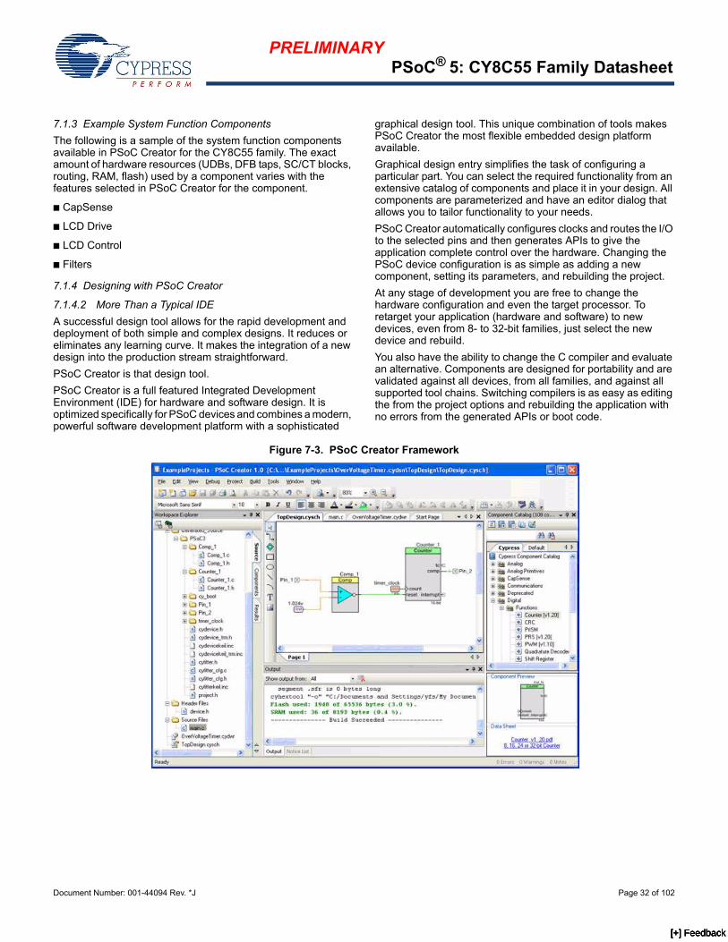
PRELIMINARYPSoC® 5: CY8C55 Family Datasheet
Document Number: 001-44094 Rev. *J Page 32 of 102
7.1.3 Example System Function Components
The following is a sample of the system function components available in PSoC Creator for the CY8C55 family. The exact amount of hardware resources (UDBs, DFB taps, SC/CT blocks, routing, RAM, flash) used by a component varies with the features selected in PSoC Creator for the component.
■ CapSense
■ LCD Drive
■ LCD Control
■ Filters
7.1.4 Designing with PSoC Creator
7.1.4.2 More Than a Typical IDE
A successful design tool allows for the rapid development and deployment of both simple and complex designs. It reduces or eliminates any learning curve. It makes the integration of a new design into the production stream straightforward.
PSoC Creator is that design tool.
PSoC Creator is a full featured Integrated Development Environment (IDE) for hardware and software design. It is optimized specifically for PSoC devices and combines a modern, powerful software development platform with a sophisticated
graphical design tool. This unique combination of tools makes PSoC Creator the most flexible embedded design platform available.
Graphical design entry simplifies the task of configuring a particular part. You can select the required functionality from an extensive catalog of components and place it in your design. All components are parameterized and have an editor dialog that allows you to tailor functionality to your needs.
PSoC Creator automatically configures clocks and routes the I/O to the selected pins and then generates APIs to give the application complete control over the hardware. Changing the PSoC device configuration is as simple as adding a new component, setting its parameters, and rebuilding the project.
At any stage of development you are free to change the hardware configuration and even the target processor. To retarget your application (hardware and software) to new devices, even from 8- to 32-bit families, just select the new device and rebuild.
You also have the ability to change the C compiler and evaluate an alternative. Components are designed for portability and are validated against all devices, from all families, and against all supported tool chains. Switching compilers is as easy as editing the from the project options and rebuilding the application with no errors from the generated APIs or boot code.
Figure 7-3. PSoC Creator Framework
[+] Feedback [+] Feedback [+] Feedback [+] Feedback

PRELIMINARYPSoC® 5: CY8C55 Family Datasheet
Document Number: 001-44094 Rev. *J Page 33 of 102
7.0.0.4 Component Catalog
Figure 7-5. Component Catalog
The component catalog is a repository of reusable design elements that select device functionality and customize your PSoC device. It is populated with an impressive selection of content; from simple primitives such as logic gates and device registers, through the digital timers, counters and PWMs, plus analog components such as ADCs, DACs, and filters, and communication protocols, such as I2C, USB and CAN. See “Example Peripherals” section on page 31 for more details about available peripherals. All content is fully characterized and carefully documented in datasheets with code examples, AC/DC specifications, and user code ready APIs.
7.0.0.6 Design Reuse
The symbol editor gives you the ability to develop reusable components that can significantly reduce future design time. Just draw a symbol and associate that symbol with your proven design. PSoC Creator allows for the placement of the new symbol anywhere in the component catalog along with the content provided by Cypress. You can then reuse your content as many times as you want, and in any number of projects, without ever having to revisit the details of the implementation.
7.0.0.7 Software Development
Figure 7-8. Code Editor
Anchoring the tool is a modern, highly customizable user interface. It includes project management and integrated editors for C and assembler source code, as well the design entry tools.
Project build control leverages compiler technology from top commercial vendors such as ARM® Limited, Keil™, and CodeSourcery (GNU). Free versions of Keil C51 and GNU C Compiler (GCC) for ARM, with no restrictions on code size or end product distribution, are included with the tool distribution. Upgrading to more optimizing compilers is a snap with support for the professional Keil C51 product and ARM RealView™ compiler.
7.0.0.9 Nonintrusive Debugging
Figure 7-10. PSoC Creator Debugger
With JTAG (4-wire) and SWD (2-wire) debug connectivity available on all devices, the PSoC Creator debugger offers full control over the target device with minimum intrusion. Breakpoints and code execution commands are all readily available from toolbar buttons and an impressive lineup of windows—register, locals, watch, call stack, memory and peripherals—make for an unparalleled level of visibility into the system. PSoC Creator contains all the tools necessary to complete a design, and then to maintain and extend that design for years to come. All steps of the design flow are carefully
[+] Feedback [+] Feedback [+] Feedback [+] Feedback

PRELIMINARYPSoC® 5: CY8C55 Family Datasheet
Document Number: 001-44094 Rev. *J Page 34 of 102
integrated and optimized for ease-of-use and to maximize productivity.
7.1 Universal Digital Block
The Universal Digital Block (UDB) represents an evolutionary step to the next generation of PSoC embedded digital peripheral functionality. The architecture in first generation PSoC digital blocks provides coarse programmability in which a few fixed functions with a small number of options are available. The new UDB architecture is the optimal balance between configuration granularity and efficient implementation. A cornerstone of this approach is to provide the ability to customize the devices digital operation to match application requirements.
To achieve this, UDBs consist of a combination of uncommitted logic (PLD), structured logic (Datapath), and a flexible routing scheme to provide interconnect between these elements, I/O connections, and other peripherals. UDB functionality ranges from simple self contained functions that are implemented in one UDB, or even a portion of a UDB (unused resources are available for other functions), to more complex functions that require multiple UDBs. Examples of basic functions are timers, counters, CRC generators, PWMs, dead band generators, and communications functions, such as UARTs, SPI, and I2C. Also, the PLD blocks and connectivity provide full featured general purpose programmable logic within the limits of the available resources.
Figure 7-11. UDB Block Diagram
The main component blocks of the UDB are:
■ PLD blocks - There are two small PLDs per UDB. These blocks take inputs from the routing array and form registered or combinational sum-of-products logic. PLDs are used to implement state machines, state bits, and combinational logic equations. PLD configuration is automatically generated from graphical primitives.
■ Datapath Module - This 8-bit wide datapath contains structured logic to implement a dynamically configurable ALU, a variety of compare configurations and condition generation. This block also contains input/output FIFOs, which are the primary parallel data interface between the CPU/DMA system and the UDB.
■ Status and Control Module - The primary role of this block is to provide a way for CPU firmware to interact and synchronize with UDB operation.
■ Clock and Reset Module - This block provides the UDB clocks and reset selection and control.
7.0.1 PLD Module
The primary purpose of the PLD blocks is to implement logic expressions, state machines, sequencers, look up tables, and decoders. In the simplest use model, consider the PLD blocks as a standalone resource onto which general purpose RTL is synthesized and mapped. The more common and efficient use model is to create digital functions from a combination of PLD and datapath blocks, where the PLD implements only the random logic and state portion of the function while the datapath (ALU) implements the more structured elements.
Figure 7-12. PLD 12C4 Structure
One 12C4 PLD block is shown in Figure 7-12. This PLD has 12 inputs, which feed across eight product terms. Each product term (AND function) can be from 1 to 12 inputs wide, and in a given product term, the true (T) or complement (C) of each input can be selected. The product terms are summed (OR function) to create the PLD outputs. A sum can be from 1 to 8 product terms wide. The 'C' in 12C4 indicates that the width of the OR gate (in this case 8) is constant across all outputs (rather than variable as in a 22V10 device). This PLA like structure gives maximum flexibility and insures that all inputs and outputs are permutable for ease of allocation by the software tools. There are two 12C4 PLDs in each UDB.
7.0.1 Datapath Module
The datapath contains an 8-bit single cycle ALU, with associated compare and condition generation logic. This datapath block is optimized to implement embedded functions, such as timers, counters, integrators, PWMs, PRS, CRC, shifters and dead band generators and many others.
PLD 12C4
(8 PTs)
PLD 12C4
(8 PTs)
Datapath
Clock and Reset
Control
Routing Channel
Datapath Chaining
PLD Chaining
Status and Control
PT
0
IN0
IN1
IN2
IN3
IN4
IN5
IN6
IN7
IN8
IN9
IN10
IN11
T C T C T C T C T C T C T C T C
T C T C T C T C T C T C T C T C
T C T C T C T C T C T C T C T C
T C T C T C T C T C T C T C T C
T C T C T C T C T C T C T C T C
T C T C T C T C T C T C T C T C
T C T C T C T C T C T C T C T C
T C T C T C T C T C T C T C T C
T C T C T C T C T C T C T C T C
T C T C T C T C T C T C T C T C
T C T C T C T C T C T C T C T C
T C T C T C T C T C T C T C T C
PT
1
PT
2
PT
3
PT
4
PT
5
PT
6
PT
7
T T T T T T T T
T T T T T T T T
T T T T T T T T
T T T T T T T T
AND Array
OR Array
MC0
MC1
MC2
OUT0
OUT1
OUT2
OUT3 MC3
SELIN(carry in)
SELOUT(carry out)
[+] Feedback [+] Feedback [+] Feedback [+] Feedback

PRELIMINARYPSoC® 5: CY8C55 Family Datasheet
Document Number: 001-44094 Rev. *J Page 35 of 102
Figure 7-13. Datapath Top Level
7.0.0.14 Working Registers
The datapath contains six primary working registers, which are accessed by CPU firmware or DMA during normal operation.
7.0.0.15 Dynamic Datapath Configuration RAM
Dynamic configuration is the ability to change the datapath function and internal configuration on a cycle-by-cycle basis, under sequencer control. This is implemented using the 8-word x 16-bit configuration RAM, which stores eight unique 16-bit wide configurations. The address input to this RAM controls the
sequence, and can be routed from any block connected to the UDB routing matrix, most typically PLD logic, I/O pins, or from the outputs of this or other datapath blocks.
ALU
The ALU performs eight general purpose functions. They are:
■ Increment
■ Decrement
■ Add
■ Subtract
■ Logical AND
■ Logical OR
■ Logical XOR
■ Pass, used to pass a value through the ALU to the shift register, mask, or another UDB register
Independent of the ALU operation, these functions are available:
■ Shift left
■ Shift right
■ Nibble swap
■ Bitwise OR mask
A0
A1
D0
D1
PI
ALU
Mask
Shift
Data Registers
Output Muxes
F1
F0
FIFOs
Accumulators
PO
A0
A1
D0
D1
Output to Programmable Routing
Chaining
Co
ntro
l Sto
re R
AM
8 W
ord
X 1
6 B
it
Parallel Input/Output(To/From Programmable Routing)
Input from Programmable
Routing
Input Muxes
To/FromNext Datapath
To/FromPrevious Datapath
Dat
apat
h C
ontr
ol
PHUB System Bus
R/W Access to All Registers
Con
ditio
ns: 2
Com
pare
s,
2 Z
ero
Det
ect,
2 O
nes
Det
ect O
verf
low
Det
ect
66
Table 7-1. Working Datapath Registers
Name Function Description
A0 and A1 Accumulators These are sources and sinks for the ALU and also sources for the compares.
D0 and D1 Data Registers These are sources for the ALU and sources for the compares.
F0 and F1 FIFOs These are the primary interface to the system bus. They can be a data source for the data registers and accumulators or they can capture data from the accumu-lators or ALU. Each FIFO is four bytes deep.
[+] Feedback [+] Feedback [+] Feedback [+] Feedback

PRELIMINARYPSoC® 5: CY8C55 Family Datasheet
Document Number: 001-44094 Rev. *J Page 36 of 102
7.0.0.16 Conditionals
Each datapath has two compares, with bit masking options. Compare operands include the two accumulators and the two data registers in a variety of configurations. Other conditions include zero detect, all ones detect, and overflow. These conditions are the primary datapath outputs, a selection of which can be driven out to the UDB routing matrix. Conditional computation can use the built in chaining to neighboring UDBs to operate on wider data widths without the need to use routing resources.
7.0.0.17 Variable MSB
The most significant bit of an arithmetic and shift function can be programmatically specified. This supports variable width CRC and PRS functions, and in conjunction with ALU output masking, can implement arbitrary width timers, counters and shift blocks.
7.0.0.18 Built in CRC/PRS
The datapath has built in support for single cycle Cyclic Redundancy Check (CRC) computation and Pseudo Random Sequence (PRS) generation of arbitrary width and arbitrary polynomial. CRC/PRS functions longer than 8 bits may be implemented in conjunction with PLD logic, or built in chaining may be use to extend the function into neighboring UDBs.
7.0.0.19 Input/Output FIFOs
Each datapath contains two four-byte deep FIFOs, which can be independently configured as an input buffer (system bus writes to the FIFO, datapath internal reads the FIFO), or an output buffer (datapath internal writes to the FIFO, the system bus reads from the FIFO). The FIFOs generate status that are selectable as datapath outputs and can therefore be driven to the routing, to interact with sequencers, interrupts, or DMA.
Figure 7-20. Example FIFO Configurations
7.0.0.21 Chaining
The datapath can be configured to chain conditions and signals such as carries and shift data with neighboring datapaths to create higher precision arithmetic, shift, CRC/PRS functions.
7.0.0.22 Time Multiplexing
In applications that are over sampled, or do not need high clock rates, the single ALU block in the datapath can be efficiently
shared with two sets of registers and condition generators. Carry and shift out data from the ALU are registered and can be selected as inputs in subsequent cycles. This provides support for 16-bit functions in one (8-bit) datapath.
7.0.0.23 Datapath I/O
There are six inputs and six outputs that connect the datapath to the routing matrix. Inputs from the routing provide the configuration for the datapath operation to perform in each cycle, and the serial data inputs. Inputs can be routed from other UDB blocks, other device peripherals, device I/O pins, and so on. The outputs to the routing can be selected from the generated conditions, and the serial data outputs. Outputs can be routed to other UDB blocks, device peripherals, interrupt and DMA controller, I/O pins, and so on.
7.0.1 Status and Control Module
The primary purpose of this circuitry is to coordinate CPU firmware interaction with internal UDB operation.
Figure 7-24. Status and Control Registers
The bits of the control register, which may be written to by the system bus, are used to drive into the routing matrix, and thus provide firmware with the opportunity to control the state of UDB processing. The status register is read-only and it allows internal UDB state to be read out onto the system bus directly from internal routing. This allows firmware to monitor the state of UDB processing. Each bit of these registers has programmable connections to the routing matrix and routing connections are made depending on the requirements of the application.
7.0.0.25 Usage Examples
As an example of control input, a bit in the control register can be allocated as a function enable bit. There are multiple ways to enable a function. In one method the control bit output would be routed to the clock control block in one or more UDBs and serve as a clock enable for the selected UDB blocks. A status example is a case where a PLD or datapath block generated a condition, such as a “compare true” condition that is captured and latched by the status register and then read (and cleared) by CPU firmware.
7.0.0.26 Clock Generation
Each subcomponent block of a UDB including the two PLDs, the datapath, and Status and Control, has a clock selection and control block. This promotes a fine granularity with respect to allocating clocking resources to UDB component blocks and allows unused UDB resources to be used by other functions for maximum system efficiency.
System Bus
F0
F1
System Bus
A0/A1/ALU
D0/D1
A0/A1/ALU
System Bus
F1
A0/A1/ALU
F0
D0
System Bus
F1
A0
D1
A1
F0
TX/RX Dual Capture Dual Buffer
Routing Channel
8-bit Status Register(Read Only)
8-bit Control Register(Write/Read)
System Bus
[+] Feedback [+] Feedback [+] Feedback [+] Feedback

PRELIMINARYPSoC® 5: CY8C55 Family Datasheet
Document Number: 001-44094 Rev. *J Page 37 of 102
7.1 UDB Array Description
Figure 7-27 shows an example of a 16 UDB array. In addition to the array core, there are a DSI routing interfaces at the top and bottom of the array. Other interfaces that are not explicitly shown include the system interfaces for bus and clock distribution. The UDB array includes multiple horizontal and vertical routing channels each comprised of 96 wires. The wire connections to UDBs, at horizontal/vertical intersection and at the DSI interface are highly permutable providing efficient automatic routing in PSoC Creator. Additionally the routing allows wire by wire segmentation along the vertical and horizontal routing to further increase routing flexibility and capability.
Figure 7-27. Digital System Interface Structure
7.0.1 UDB Array Programmable Resources
Figure 7-28 shows an example of how functions are mapped into a bank of 16 UDBs. The primary programmable resources of the UDB are two PLDs, one datapath and one status/control register. These resources are allocated independently, because they have independently selectable clocks, and therefore unused blocks are allocated to other unrelated functions.
An example of this is the 8-bit Timer in the upper left corner of the array. This function only requires one datapath in the UDB, and therefore the PLD resources may be allocated to another function. A function such as a Quadrature Decoder may require more PLD logic than one UDB can supply and in this case can
utilize the unused PLD blocks in the 8-bit Timer UDB. Programmable resources in the UDB array are generally homogeneous so functions can be mapped to arbitrary boundaries in the array.
Figure 7-28. Function Mapping Example in a Bank of UDBs
7.1 DSI Routing Interface Description
The DSI routing interface is a continuation of the horizontal and vertical routing channels at the top and bottom of the UDB array core. It provides general purpose programmable routing between device peripherals, including UDBs, I/Os, analog peripherals, interrupts, DMA and fixed function peripherals.
Figure 7-29 illustrates the concept of the digital system interconnect, which connects the UDB array routing matrix with other device peripherals. Any digital core or fixed function peripheral that needs programmable routing is connected to this interface.
Signals in this category include:
■ Interrupt requests from all digital peripherals in the system.
■ DMA requests from all digital peripherals in the system.
■ Digital peripheral data signals that need flexible routing to I/Os.
■ Digital peripheral data signals that need connections to UDBs.
■ Connections to the interrupt and DMA controllers.
■ Connection to I/O pins.
■ Connection to analog system digital signals.
UDB
UDB
HVB
UDB
UDB
HVA
UDB
UDB
HVB
HVA
UDB
UDB
HVA
UDB
UDB
HVB
UDB
UDB
HVA
HVB
HVB
HVA
HVB
HVA
HVA
HVB
HVA
HVB
UDB
UDB
UDB
UDB
System Connections
System Connections
UDB
UDB
HVB
UDB
UDB
HVA
UDB
UDB
HVB
HVA
UDB
HVA
UDB
HVB
UDB
HVA
HVB
UDB
UDB
UDBUDBUDB UDB
UART
Logic
12-Bit PWM
I2C Slave8-Bit SPI
12-Bit SPI
Logic8-Bit Timer
16-Bit PYRS
UDB
8-Bit Timer
Quadrature Decoder 16-Bit PWM
Se
qu
en
ce
r
[+] Feedback [+] Feedback [+] Feedback [+] Feedback

PRELIMINARYPSoC® 5: CY8C55 Family Datasheet
Document Number: 001-44094 Rev. *J Page 38 of 102
Figure 7-29. Digital System Interconnect
Interrupt and DMA routing is very flexible in the CY8C55 programmable architecture. In addition to the numerous fixed function peripherals that can generate interrupt requests, any data signal in the UDB array routing can also be used to generate a request. A single peripheral may generate multiple independent interrupt requests simplifying system and firmware design. Figure 7-30 shows the structure of the IDMUX (Interrupt/DMA Multiplexer).
Figure 7-30. Interrupt and DMA Processing in the IDMUX
7.0.1 I/O Port Routing
There are a total of 20 DSI routes to a typical 8-bit I/O port, 16 for data and four for drive strength control.
When an I/O pin is connected to the routing, there are two primary connections available, an input and an output. In conjunction with drive strength control, this can implement a bidirectional I/O pin. A data output signal has the option to be single synchronized (pipelined) and a data input signal has the
option to be double synchronized. The synchronization clock is the system clock (see Figure 6-1). Normally all inputs from pins are synchronized as this is required if the CPU interacts with the signal or any signal derived from it. Asynchronous inputs have rare uses. An example of this is a feed through of combinational PLD logic from input pins to output pins.
Figure 7-31. I/O Pin Synchronization Routing
Figure 7-32. I/O Pin Output Connectivity
There are four more DSI connections to a given I/O port to implement dynamic output enable control of pins. This connectivity gives a range of options, from fully ganged 8-bits controlled by one signal, to up to four individually controlled pins. The output enable signal is useful for creating tri-state bidirectional pins and buses.
Figure 7-33. I/O Pin Output Enable Connectivity
UDB ARRAY
Digital System Routing I/F
Digital System Routing I/F
CANInterrupt
ControllerI2C
IO Port Pins
DMAController
GlobalClocks
Delta-Sigma ADC
ComparatorsDACSSC
Blocks
IO Port Pins
EMIFGlobalClocks
TimerCounters
SAR ADC
DMA termout (IRQs)
DMA Controller
Interrupt Controller
Fixed Function IRQs
Edge Detect
Edge Detect
IRQs
UDB Array
Fixed Function DRQs
DRQs
Interrupt and DMA Processing in IDMUX
0
1
2
3
0
1
2
DO
DI
Port i
PIN 0DO
PIN1DO
PIN2DO
PIN3DO
PIN4DO
PIN5DO
PIN6DO
PIN7DO
8 IO Data Output Connections from the UDB Array Digital System Interface
Port i
PIN 0OE
PIN1OE
PIN2OE
PIN3OE
PIN4OE
PIN5OE
PIN6OE
PIN7OE
4 IO Control Signal Connections from UDB Array Digital System Interface
[+] Feedback [+] Feedback [+] Feedback [+] Feedback

PRELIMINARYPSoC® 5: CY8C55 Family Datasheet
Document Number: 001-44094 Rev. *J Page 39 of 102
7.1 CAN
The CAN peripheral is a fully functional Controller Area Network (CAN) supporting communication baud rates up to 1 Mbps. The CAN controller implements the CAN2.0A and CAN2.0B specifications as defined in the Bosch specification and conforms to the ISO-11898-1 standard. The CAN protocol was originally designed for automotive applications with a focus on a high level of fault detection. This ensures high communication
reliability at a low cost. Because of its success in automotive applications, CAN is used as a standard communication protocol for motion oriented machine control networks (CANOpen) and factory automation applications (DeviceNet). The CAN controller features allow the efficient implementation of higher level protocols without affecting the performance of the microcontroller CPU. Full configuration support is provided in PSoC Creator.
Figure 7-34. CAN Bus System Implementation
7.0.1 CAN Features
■ CAN2.0A/B protocol implementation - ISO 11898 compliant❐ Standard and extended frames with up to 8 bytes of data per
frame❐ Message filter capabilities❐ Remote Transmission Request (RTR) support❐ Programmable bit rate up to 1 Mbps
■ Listen Only mode
■ SW readable error counter and indicator
■ Sleep mode: Wake the device from sleep with activity on the Rx pin
■ Supports two or three wire interface to external transceiver (Tx, Rx, and Enable). The three-wire interface is compatible with the Philips PHY; the PHY is not included on-chip. The three wires can be routed to any I/O
■ Enhanced interrupt controller❐ CAN receive and transmit buffers status❐ CAN controller error status including BusOff
■ Receive path❐ 16 receive buffers each with its own message filter❐ Enhanced hardware message filter implementation that
covers the ID, IDE and RTR❐ DeviceNet addressing support❐ Multiple receive buffers linkable to build a larger receive
message array❐ Automatic transmission request (RTR) response handler❐ Lost received message notification
■ Transmit path❐ Eight transmit buffers❐ Programmable transmit priority❐ Round robin❐ Fixed priority❐ Message transmissions abort capability
7.0.2 Software Tools Support
CAN Controller configuration integrated into PSoC Creator:
■ CAN Configuration walkthrough with bit timing analyzer
■ Receive filter setup
CAN Node 1
PSoC
CAN Controller
CAN Transceiver
Tx RxEn
CAN Node 2 CAN Node n
CAN_H CAN_L CAN_H CAN_L CAN_H CAN_L
CAN Drivers
CAN Bus
[+] Feedback [+] Feedback [+] Feedback [+] Feedback
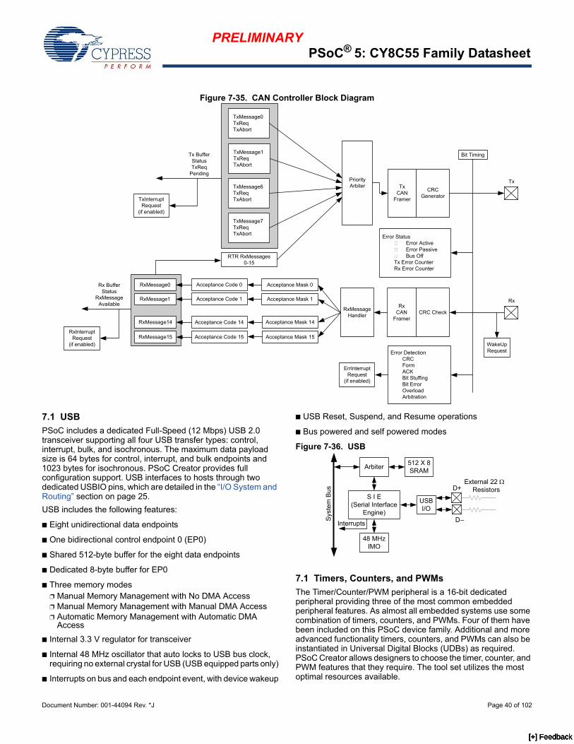
PRELIMINARYPSoC® 5: CY8C55 Family Datasheet
Document Number: 001-44094 Rev. *J Page 40 of 102
Figure 7-35. CAN Controller Block Diagram
7.1 USB
PSoC includes a dedicated Full-Speed (12 Mbps) USB 2.0 transceiver supporting all four USB transfer types: control, interrupt, bulk, and isochronous. The maximum data payload size is 64 bytes for control, interrupt, and bulk endpoints and 1023 bytes for isochronous. PSoC Creator provides full configuration support. USB interfaces to hosts through two dedicated USBIO pins, which are detailed in the “I/O System and Routing” section on page 25.
USB includes the following features:
■ Eight unidirectional data endpoints
■ One bidirectional control endpoint 0 (EP0)
■ Shared 512-byte buffer for the eight data endpoints
■ Dedicated 8-byte buffer for EP0
■ Three memory modes❐ Manual Memory Management with No DMA Access❐ Manual Memory Management with Manual DMA Access❐ Automatic Memory Management with Automatic DMA
Access
■ Internal 3.3 V regulator for transceiver
■ Internal 48 MHz oscillator that auto locks to USB bus clock, requiring no external crystal for USB (USB equipped parts only)
■ Interrupts on bus and each endpoint event, with device wakeup
■ USB Reset, Suspend, and Resume operations
■ Bus powered and self powered modes
Figure 7-36. USB
7.1 Timers, Counters, and PWMs
The Timer/Counter/PWM peripheral is a 16-bit dedicated peripheral providing three of the most common embedded peripheral features. As almost all embedded systems use some combination of timers, counters, and PWMs. Four of them have been included on this PSoC device family. Additional and more advanced functionality timers, counters, and PWMs can also be instantiated in Universal Digital Blocks (UDBs) as required. PSoC Creator allows designers to choose the timer, counter, and PWM features that they require. The tool set utilizes the most optimal resources available.
TxMessage0TxReqTxAbort
TxMessage7TxReqTxAbort
TxMessage1TxReqTxAbort
TxMessage6TxReqTxAbort
Priority Arbiter
RxMessage0
RxMessage15
RxMessage1
RxMessage14
RxMessage Handler
Acceptance Code 0 Acceptance Mask 0
Acceptance Code 1 Acceptance Mask 1
Acceptance Code 14 Acceptance Mask 14
Acceptance Code 15 Acceptance Mask 15
RTR RxMessages 0-15
TxCAN
Framer
CRC Generator
RxCAN
FramerCRC Check
Bit Timing
Error DetectionCRCFormACKBit StuffingBit ErrorOverloadArbitration
TxInterrupt Request
(if enabled)
RxInterrupt Request
(if enabled)
Error StatusError ActiveError PassiveBus Off
Tx Error CounterRx Error Counter
ErrInterrupt Request
(if enabled)
WakeUp Request
Rx Buffer Status
RxMessage Available
Tx Buffer StatusTxReq
Pending
Rx
Tx
S I E (Serial Interface
Engine)
48 MHz IMO
Arbiter512 X 8 SRAM
USB I/O
D+
D–Interrupts
Sys
tem
Bu
s
External 22 Resistors
[+] Feedback [+] Feedback [+] Feedback [+] Feedback

PRELIMINARYPSoC® 5: CY8C55 Family Datasheet
Document Number: 001-44094 Rev. *J Page 41 of 102
The Timer/Counter/PWM peripheral can select from multiple clock sources, with input and output signals connected through the DSI routing. DSI routing allows input and output connections to any device pin and any internal digital signal accessible through the DSI. Each of the four instances has a compare output, terminal count output (optional complementary compare output), and programmable interrupt request line. The Timer/Counter/PWMs are configurable as free running, one shot, or Enable input controlled. The peripheral has timer reset and capture inputs, and a kill input for control of the comparator outputs. The peripheral supports full 16-bit capture.
Timer/Counter/PWM features include:
■ 16-bit timer/counter/PWM (down count only)
■ Selectable clock source
■ PWM comparator (configurable for LT, LTE, EQ, GTE, GT)
■ Period reload on start, reset, and terminal count
■ Interrupt on terminal count, compare true, or capture
■ Dynamic counter reads
■ Timer capture mode
■ Count while enable signal is asserted mode
■ Free run mode
■ One-shot mode (stop at end of period)
■ Complementary PWM outputs with deadband
■ PWM output kill
Figure 7-37. Timer/Counter/PWM
7.1 I2C
The I2C peripheral provides a synchronous two wire interface designed to interface the PSoC device with a two wire I2C serial communication bus. The bus is compliant with Philips ‘The I2C Specification’ version 2.1. Additional I2C interfaces can be instantiated using Universal Digital Blocks (UDBs) in PSoC Creator, as required.
To eliminate the need for excessive CPU intervention and overhead, I2C specific support is provided for status detection and generation of framing bits. I2C operates as a slave, a master, or multimaster (Slave and Master). In slave mode, the unit always listens for a start condition to begin sending or receiving data. Master mode supplies the ability to generate the Start and Stop conditions and initiate transactions. Multimaster mode provides clock synchronization and arbitration to allow multiple masters on the same bus. If Master mode is enabled and Slave mode is not enabled, the block does not generate interrupts on externally generated Start conditions. I2C interfaces through the DSI routing and allows direct connections to any GPIO or SIO pins.
I2C provides hardware address detect of a 7-bit address without CPU intervention. Additionally the device can wake from low power modes on a 7-bit hardware address match. If wakeup functionality is required, I2C pin connections are limited to the two special sets of SIO pins.
I2C features include:
■ Slave and Master, Transmitter, and Receiver operation
■ Byte processing for low CPU overhead
■ Interrupt or polling CPU interface
■ Support for bus speeds up to 1 Mbps (3.4 Mbps in UDBs)
■ 7 or 10-bit addressing (10-bit addressing requires firmware support)
■ SMBus operation (through firmware support - SMBus supported in hardware in UDBs)
■ 7-bit hardware address compare
■ Wake from low power modes on address match
7.2 Digital Filter Block
Some devices in the CY8C55 family of devices have a dedicated HW accelerator block used for digital filtering. The DFB has a dedicated multiplier and accumulator that calculates a 24-bit by 24-bit multiply accumulate in one system clock cycle. This enables the mapping of a direct form FIR filter that approaches a computation rate of one FIR tap for each clock cycle. The MCU can implement any of the functions performed by this block, but at a slower rate that consumes significant MCU bandwidth.
The PSoC Creator interface provides a wizard to implement FIR and IIR digital filters with coefficients for LPF, BPF, HPF, Notch and arbitrary shape filters. 64 pairs of data and coefficients are stored. This enables a 64 tap FIR filter or up to 4 16 tap filters of either FIR or IIR formulation.
Figure 7-38. DFB Application Diagram (pwr/gnd not shown)
The typical use model is for data to be supplied to the DFB over the system bus from another on-chip system data source such as an ADC. The data typically passes through main memory or is directly transferred from another chip resource through DMA. The DFB processes this data and passes the result to another on chip resource such as a DAC or main memory through DMA on the system bus.
Data movement in or out of the DFB is typically controlled by the system DMA controller but can be moved directly by the MCU.
Timer / Counter / PWM 16-bit
ClockResetEnableCaptureKill
IRQ
Compare
TC / Compare!
Digital Filter Block
write_data
read_data
SystemBus
DMACTRL
DataSource (PHUB)
DataDest
(PHUB)
addrDigital
Routing
BUSCLK
DMA Request
[+] Feedback [+] Feedback [+] Feedback [+] Feedback

PRELIMINARYPSoC® 5: CY8C55 Family Datasheet
Document Number: 001-44094 Rev. *J Page 42 of 102
8. Analog Subsystem
The analog programmable system creates application specific combinations of both standard and advanced analog signal processing blocks. These blocks are then interconnected to each other and also to any pin on the device, providing a high level of design flexibility and IP security. The features of the analog subsystem are outlined here to provide an overview of capabilities and architecture.
■ Flexible, configurable analog routing architecture provided by analog globals, analog mux bus, and analog local buses
■ High resolution Delta-Sigma ADC
■ Two successive approximation (SAR) ADCs
■ Four 8-bit DACs that provide either voltage or current output
■ Four comparators with optional connection to configurable LUT outputs
■ Four configurable switched capacitor/continuos time (SC/CT) blocks for functions that include opamp, unity gain buffer, programmable gain amplifier, transimpedance amplifier, and mixer
■ Four opamps for internal use and connection to GPIO that can be used as high current output buffers
■ CapSense subsystem to enable capacitive touch sensing
■ Precision reference for generating an accurate analog voltage for internal analog blocks
Figure 8-1. Analog Subsystem Block Diagram
The PSoC Creator software program provides a user friendly interface to configure the analog connections between the GPIO and various analog resources and also connections from one analog resource to another. PSoC Creator also provides component libraries that allow you to configure the various analog blocks to perform application specific functions (PGA, transimpedance amplifier, voltage DAC, current DAC, and so on). The tool also generates API interface libraries that allow you to write firmware that allows the communication between the analog peripheral and CPU/Memory.
8.1 Analog Routing
The CY8C38 family of devices has a flexible analog routing architecture that provides the capability to connect GPIOs and
different analog blocks, and also route signals between different analog blocks. One of the strong points of this flexible routing architecture is that it allows dynamic routing of input and output connections to the different analog blocks.
8.1.1 Features
■ Flexible, configurable analog routing architecture
■ 16 analog globals (AG) and two analog mux buses (AMUXBUS) to connect GPIOs and the analog blocks
■ Each GPIO is connected to one analog global and one analog mux bus
Analog Interface
SC/CT Block
CMP CMPCMPCMP
CapSense Subsystem
DSI Array
Clock Distribution
Decimator
Config & Status
RegistersPHUB CPU
Comparators
GPIO Port
GPIO Port
DACDAC
DelS
ig
AD
C
DAC DAC
Op
Am
pO
pA
mp
ANALOG
ROUTING
ANALOG
ROUTING
Op
Am
pO
pA
mp
SC/CT Block
SC/CT BlockSC/CT Block
SARADC
SARADC
Precision Reference
[+] Feedback [+] Feedback [+] Feedback [+] Feedback

PRELIMINARYPSoC® 5: CY8C55 Family Datasheet
Document Number: 001-44094 Rev. *J Page 43 of 102
■ Eight analog local buses (abus) to route signals between the different analog blocks
■ Multiplexers and switches for input and output selection of the analog blocks
8.1.2 Functional Description
Analog globals (AGs) and analog mux buses (AMUXBUS) provide analog connectivity between GPIOs and the various analog blocks. There are 16 AGs in the CY8C38 family. The
analog routing architecture is divided into four quadrants as shown in Figure 8-1. Each quadrant has four analog globals (AGL[0..3], AGL[4..7], AGR[0..3], AGR[4..7]). Each GPIO is connected to the corresponding AG through an analog switch. The analog mux bus is a shared routing resource that connects to every GPIO through an analog switch. There are two AMUXBUS routes in CY8C38, one in the left half (AMUXBUSL) and one in the right half (AMUXBUSR), as shown in Figure 8-1.
Figure 8-1. CY8C55 Analog Interconnect
Vd
dio0
SIO
P1
2[3
]
SIO
P1
2[2
]
GP
IOP
15[3
]
GP
IOP
15[2
]
SIO
P1
2[1]
SIO
P1
2[0]
GP
IOP
3[7]
GP
IOP
3[6]
Vd
dio3
Vccd
Vssd
Vddd
GPIOP6[0]
GPIOP6[3]
GPIOP6[2]
GPIOP6[1]
GPIOP15[4]GPIOP15[5]GPIOP2[0]
GPIOP2[4]
GPIOP2[3]
GPIOP2[2]
GPIOP2[1]
Vddio2
GP
IOP
2[5]
GP
IOP
2[7]
GP
IOP
2[6]
SIO
P1
2[4
]S
IOP
12[
5]
GP
IOP
6[4]
GP
IOP
6[5]
GP
IOP
6[6]
GP
IOP
6[7]
Vd
dio1
SIOP12[6]
SIOP12[7]
USB IOP15[6]
USB IOP15[7]
Vddd
Vssd
Vccd
GPXTP15[0]
GPXTP15[1]
GPIOP3[5]GPIOP3[4]GPIOP3[3]GPIOP3[2]GPIOP3[1]
AGR[4]
AGR[7]
AGR[6]
AGR[5]
AGL[0]
AGL[3]
AGL[2]
AGL[1]AGR[0]
AGR[3]
AGR[2]
AGR[1]
* * *
*
*
*
*
**
*
*
* Denotes pins on all packages
DSM
v0
v2
v1
v3
i1
i3
i0
i2
VIDAC
76543210
76543210
76543210
76543210
comp0
comp2
comp1
comp3
COMPARATOR
AG
L[4]
AG
L[7]
AG
L[6]
AG
L[5]
AG
L[0]
AG
L[3]
AG
L[2]
AG
L[1] A
GR
[0]
AG
R[3
]
AG
R[2
]
AG
R[1
]
AG
R[4
]
AG
R[7
]
AG
R[6
]
AG
R[5
]
Notes:
AMUXBUSRAMUXBUSL
i1
i3i2
i0
Rev #512-April-2010
opamp0
Vssa
Vssd
Vcca
GPIOP0[5]
*
GPIOP0[7] *
GP
IOP
1[3
]
GP
IOP
1[2
]
GP
IOP
1[1
]
GP
IOP
1[0
]
* * * *
GP
IOP
1[4
]*
GP
IOP
1[5
]*
GPIOP1[6]*
GPIOP1[7]*
GPIOP5[7]GPIOP5[6]GPIOP5[5]GPIOP5[4]
GPIOP4[4]
GPIOP4[7]
GPIOP4[6]
GPIOP4[5]
GP
IOP
5[2
]G
PIO
P5
[3]
GP
IOP
5[1
]
GP
IOP
5[0
]
GPIOP4[3]
GPIOP4[2]
ABUSL0
*
* **
* *
*
*
*
*
*
*
*
*
*
AGL[4]
AGL[7]
AGL[6]
AGL[5]
GP
IOP
4[0]G
PIO
P4[1]
vssa
AMUXBUSL AMUXBUSR
AM
UX
BU
SL
AM
UX
BU
SR
AMUXBUSL AMUXBUSR
ABUSL1ABUSL2ABUSL3 ABUSR3
ABUSR2ABUSR1ABUSR0
ExVrefL
ExVrefR
Ind
Vss
b
Vbo
ost
XR
ES
Vss
d
* * * *
Vb
at
ExVrefRExVrefL
90
36
28
13
44
+
-
qtz_refrefs
GPIOP3[0]
GPIOP0[6] *
LPFin0
out0
in1
out15
sc0 sc1
sc2 sc3
VinVrefout
out
outSC/CT
out104
Mux GroupSwitch Group
Connection
Large ( ~200 Ohms)
Small ( ~870 Ohms )
Switch Resistance
VinVref
VinVref
VinVref
Vss refTS
ADC
GP
IOP
0[0] *
GP
IOP
0[1] *
GP
IOP
0[2] *
GP
IOP
0[3] *
GPIOP0[4]
*
AM
UX
BU
SR
AM
UX
BU
SL
ANALOG GLOBALS
ANALOGBUS
0123 3210ANALOG
BUSANALOG GLOBALS
refbufrrefbuflin
outref
in
outref
vssa
CAPSENSE
Vssa
SAR ADC
Vp (+)Vn (-)
(+) Vp(-) Vn
ExVrefL2ExVrefL1
refs refsVrefhi_outVrefhi_out
ExVrefL1opamp2 opamp3 opamp1
ExVrefL2
cmp0_vref (1.024V)
vref_cmp1 (0.256V)
Vdda
sc0_bgref (1.024V)
refbuf_vref1 (1.024V)
refbuf_vref2 (1.2V)
dac_vref (0.256V)
dsm0_vcm_vref1(0.8V)
dsm0_qtz_vref2 (1.2V)
SAR_vref2 (1.2V)SAR_vref1 (1.024V)
abuf_vref_int (1.024V)
32100123
CY8C55 only
LCD signals are not shown.
*
:
Vdda *
VBE
vref_vss_ext
sc1_bgref (1.024V)
sc2_bgref (1.024V)
sc3_bgref (1.024V)
en_resvda
en_resvpwra
dsm0_vcm_vref2 (0.7V)
vcmsel[1:0]
vpwravpwra/2
VddaVdda/4
refmux[2:0]
dsm0_qtz_vref1 (1.024V)
VddaVdda/2
refmux[2:0]en_resvda
SAR_vref2 (1.2V)SAR_vref1 (1.024V)
VddaVdda/2
refmux[2:0]en_resvda
vcm
DAC0
DAC2
DAC1
DAC3
DSM0
+-
+-
+-
+-
SAR0 SAR1
cmp_muxvn[1:0]
Vdda/2bg_vda_swabusl0
cmp1
_vre
f
cmp1
_vre
f
cmp1_vref
refsel[1:0]
refb
ufl_
cmp
refb
ufr
_cm
p
cmp0_vref (1.024V)
abuf_vref_int (1.024V)
bg_vda_res_en
refbuf_vref1 (1.024V)
refbuf_vref2 (1.2V)
refsel[1:0]
swout
swin
swout
swin
swfol swfolswfol swfol
swinn
swinn
swinp
swinp
swinp
swinn
swinp
swinn
LPF
[+] Feedback [+] Feedback [+] Feedback [+] Feedback

PRELIMINARYPSoC® 5: CY8C55 Family Datasheet
Document Number: 001-44094 Rev. *J Page 44 of 102
Analog local buses (abus) are routing resources located within the analog subsystem and are used to route signals between different analog blocks. There are eight abus routes in CY8C38, four in the left half (abusl [0:3]) and four in the right half (abusr [0:3]) as shown in Figure 8-1. Using the abus saves the analog globals and analog mux buses from being used for interconnecting the analog blocks.
Multiplexers and switches exist on the various buses to direct signals into and out of the analog blocks. A multiplexer can have only one connection on at a time, whereas a switch can have multiple connections on simultaneously. In Figure 8-1, multiplexers are indicated by grayed ovals and switches are indicated by transparent ovals.
8.1 Delta-sigma ADC
The CY8C38 device contains one delta-sigma ADC. This ADC offers differential input, high resolution and excellent linearity, making it a good ADC choice for both audio signal processing and measurement applications. The converter's nominal operation is 16 bits at 48 ksps. The ADC can be configured to output 20-bit resolution at data rates of up to 187 sps. At a fixed clock rate, resolution can be traded for faster data rates as shown in Table 8-1 and Figure 8-2.
Figure 8-2. Delta-sigma ADC Sample Rates, Range = ±1.024 V
8.0.1 Functional Description
The ADC connects and configures three basic components, input buffer, delta-sigma modulator, and decimator. The basic block diagram is shown in Figure 8-1. The signal from the input muxes is delivered to the delta-sigma modulator either directly or through the input buffer. The delta-sigma modulator performs the
actual analog to digital conversion. The modulator over-samples the input and generates a serial data stream output. This high speed data stream is not useful for most applications without some type of post processing, and so is passed to the decimator through the Analog Interface block. The decimator converts the high speed serial data stream into parallel ADC results. The modulator/decimator frequency response is [(sin x)/x]4; a typical frequency response is shown in Figure 8-2.
Figure 8-1. Delta-sigma ADC Block Diagram
Figure 8-2. Delta-sigma ADC Frequency Response, Normalized to Output, Sample Rate = 48 kHz
Resolution and sample rate are controlled by the Decimator. Data is pipelined in the decimator; the output is a function of the last four samples. When the input multiplexer is switched, the output data is not valid until after the fourth sample after the switch.
8.0.1 Operational Modes
The ADC can be configured by the user to operate in one of four modes: Single Sample, Multi Sample, Continuos, or Multi Sample (Turbo). All four modes are started by either a write to the start bit in a control register or an assertion of the Start of Conversion (SoC) signal. When the conversion is complete, a status bit is set and the output signal End of Conversion (EoC) asserts high and remains high until the value is read by either the DMA controller or the CPU.
8.0.1.1 Single Sample
In Single Sample mode, the ADC performs one sample conversion on a trigger. In this mode, the ADC stays in standby state waiting for the SoC signal to be asserted. When SoC is signaled the ADC performs four successive conversions. The first three conversions prime the decimator. The ADC result is
Table 8-1. Delta-sigma ADC Performance
Bits Maximum Sample Rate (sps) SNR (dB)
20 187 110
16 48 k 89
12 192 k 70
8 384 k TBD
Sa
mp
le r
ate
(S
PS
)
1
10
100
1000
10000
100000
1000000
6 8 10 12 14 16 18 20 22Resolution, bits
ContinuousMulti-SampleMulti-SampleTurbo
Delta Sigma
ModulatorDecimator 12 to 20 Bit
Result
EOC
SOC
PositiveInput Mux
NegativeInput Mux
(Analog Routing)InputBuffer
freq
uenc
y R
espo
nse.
dB
-100
-90
-80
-70
-60
-50
-40
-30
-20
-10
0
100 1,000 10,000 100,000 1,000,000Input Frequency, HzInput Frequency, Hz
[+] Feedback [+] Feedback [+] Feedback [+] Feedback

PRELIMINARYPSoC® 5: CY8C55 Family Datasheet
Document Number: 001-44094 Rev. *J Page 45 of 102
valid and available after the fourth conversion, at which time the EoC signal is generated. To detect the end of conversion, the system may poll a control register for status or configure the external EoC signal to generate an interrupt or invoke a DMA request. When the transfer is done the ADC reenters the standby state where it stays until another SoC event.
8.0.1.2 Continuous
Continuous sample mode is used to take multiple successive samples of a single input signal. Multiplexing multiple inputs should not be done with this mode. There is a latency of three conversion times before the first conversion result is available. This is the time required to prime the decimator. After the first result, successive conversions are available at the selected sample rate.
8.0.1.3 Multi Sample
Multi sample mode is similar to continuous mode except that the ADC is reset between samples. This mode is useful when the input is switched between multiple signals. The decimator is re-primed between each sample so that previous samples do not affect the current conversion. Upon completion of a sample, the next sample is automatically initiated. The results can be transferred using either firmware polling, interrupt, or DMA.
8.0.1.4 Multi Sample (Turbo)
The multi sample (turbo) mode operates identical to the Multi-sample mode for resolutions of 8 to 16 bits. For resolutions of 17 to 20 bits, the performance is about four times faster than the multi sample mode, because the ADC is only reset once at the end of conversion.
More information on output formats is provided in the Technical Reference Manual.
8.0.2 Start of Conversion Input
The SoC signal is used to start an ADC conversion. A digital clock or UDB output can be used to drive this input. It can be used when the sampling period must be longer than the ADC conversion time or when the ADC must be synchronized to other hardware. This signal is optional and does not need to be connected if ADC is running in a continuous mode.
8.0.3 End of Conversion Output
The EoC signal goes high at the end of each ADC conversion. This signal may be used to trigger either an interrupt or DMA request.
8.1 Successive Approximation ADC
The CY8C55 family of devices has two Successive Approximation (SAR) ADCs. These ADCs are 12-bit at up to 1 Msps, with single-ended or differential inputs, making them useful for a wide variety of sampling and control applications.
8.1.1 Functional Description
In a SAR ADC an analog input signal is sampled and compared with the output of a DAC. A binary search algorithm is applied to the DAC and used to determine the output bits in succession from MSB to LSB. A block diagram of one SAR ADC is shown in Figure 8-1.
Figure 8-1. SAR ADC Block Diagram
The input is connected to the analog globals and muxes. The frequency of the clock is 16 times the sample rate; the maximum clock rate is 16 MHz.
8.0.1 Conversion Signals
Writing a start bit or assertion of a start of frame (SOF) signal is used to start a conversion. SOF can be used in applications where the sampling period is longer than the conversion time, or when the ADC needs to be synchronized to other hardware. This signal is optional and does not need to be connected if the SAR ADC is running in a continuous mode. A digital clock or UDB output can be used to drive this input. When the SAR is first powered up or awakened from any of the sleeping modes, there is a power up wait time of 10 µs before it is ready to start the first conversion.
When the conversion is complete, a status bit is set and the output signal end of frame (EOF) asserts and remains asserted until the value is read by either the DMA controller or the CPU. The EOF signal may be used to trigger an interrupt or a DMA request.
8.0.2 Operational Modes
A ONE_SHOT control bit is used to set the SAR ADC conversion mode to either continuous or one conversion per SOF signal. DMA transfer of continuous samples, without CPU intervention, is supported.
8.1 Comparators
The CY8C55 family of devices contains four comparators. Comparators have these features:
■ Input offset factory trimmed to less than 5 mV
■ Rail-to-rail common mode input range (VSSA to VCCA)
■ Speed and power can be traded off by using one of three modes: fast, slow, or ultra low power
■ Comparator outputs can be routed to look up tables to perform simple logic functions and then can also be routed to digital blocks
■ The positive input of the comparators may be optionally passed through a low pass filter. Two filters are provided
■ Comparator inputs can be connections to GPIO, DAC outputs and SC block outputs
S/HDACarray
vin
vrefp vrefn
comparatorSARdigital D0:D11
clock
autozeroresetclock
D0:
D11
powerfiltering
POWERGROUND
vrefp vrefn
[+] Feedback [+] Feedback [+] Feedback [+] Feedback

PRELIMINARYPSoC® 5: CY8C55 Family Datasheet
Document Number: 001-44094 Rev. *J Page 46 of 102
8.1.1 Input and Output Interface
The positive and negative inputs to the comparators come from the analog global buses, the analog mux line, the analog local
bus and precision reference through multiplexers. The output from each comparator could be routed to any of the two input LUTs. The output of that LUT is routed to the UDB DSI.
Figure 8-2. Analog Comparator
8.0.1 LUT
The CY8C55 family of devices contains four LUTs. The LUT is a two input, one output lookup table that is driven by any one or two of the comparators in the chip. The output of any LUT is routed to the digital system interface of the UDB array. From the digital system interface of the UDB array, these signals can be connected to UDBs, DMA controller, I/O, or the interrupt controller.
The LUT control word written to a register sets the logic function on the output. The available LUT functions and the associated control word is shown in Table 8-1.
ANAIF
+
_
+
+_
comp2_
comp0comp1
+
_comp3
4
LUT0 LUT1 LUT2 LUT3
4 4 4 4 4 4 4
From Analog
Routing
From Analog
Routing
From Analog
Routing
From Analog
Routing
UDBs
Table 8-1. LUT Function vs. Program Word and Inputs
Control Word Output (A and B are LUT inputs)
0000b FALSE (‘0’)
0001b A AND B
0010b A AND (NOT B)
0011b A
0100b (NOT A) AND B
0101b B
0110b A XOR B
0111b A OR B
1000b A NOR B
1001b A XNOR B
1010b NOT B
1011b A OR (NOT B)
1100b NOT A
1101b (NOT A) OR B
1110b A NAND B
1111b TRUE (‘1’)
[+] Feedback [+] Feedback [+] Feedback [+] Feedback

PRELIMINARYPSoC® 5: CY8C55 Family Datasheet
Document Number: 001-44094 Rev. *J Page 47 of 102
8.1 Opamps
The CY8C55 family of devices contain four general purpose opamps.
Figure 8-3. Opamp
The opamp is uncommitted and can be configured as a gain stage or voltage follower on external or internal signals.
See Figure 8-4. In any configuration, the input and output signals can all be connected to the internal global signals and monitored with an ADC, or comparator. The configurations are implemented with switches between the signals and GPIO pins.
Figure 8-4. Opamp Configurations
The opamp has three speed modes, slow, medium, and fast. The slow mode consumes the least amount of quiescent power and the fast mode consumes the most power. The inputs are able to swing rail-to-rail. The output swing is capable of rail-to-rail
operation at low current output, within 50 mV of the rails. When driving high current loads (about 25 mA) the output voltage may only get within 500 mV of the rails.
8.1 Programmable SC/CT Blocks
The CY8C55 family of devices contains four switched capacitor/continuous time (SC/CT) blocks. Each switched capacitor/continuous time block is built around a single rail-to-rail high bandwidth opamp.
Switched capacitor is a circuit design technique that uses capacitors plus switches instead of resistors to create analog functions. These circuits work by moving charge between capacitors by opening and closing different switches. Nonoverlapping in phase clock signals control the switches, so that not all switches are ON simultaneously.
The PSoC Creator tool offers a user friendly interface, which allows you to easily program the SC/CT blocks. Switch control and clock phase control configuration is done by PSoC Creator so users only need to determine the application use parameters such as gain, amplifier polarity, VREF connection, and so on.
The same opamps and block interfaces are also connectable to an array of resistors which allows the construction of a variety of continuous time functions.
The opamp and resistor array is programmable to perform various analog functions including
■ Naked Operational Amplifier - Continuous Mode
■ Unity-Gain Buffer - Continuous Mode
■ Programmable Gain Amplifier (PGA) - Continuous Mode
■ Transimpedance Amplifier (TIA) - Continuous Mode
■ Up/Down Mixer - Continuous Mode
■ Sample and Hold Mixer (NRZ S/H) - Switched Cap Mode
■ First Order Analog to Digital Modulator - Switched Cap Mode
8.1.1 Naked Opamp
The Naked Opamp presents both inputs and the output for connection to internal or external signals. The opamp has a unity gain bandwidth greater than 6.0 MHz and output drive current up to 650 µA. This is sufficient for buffering internal signals (such as DAC outputs) and driving external loads greater than 7.5 kohms.
8.1.2 Unity Gain
The Unity Gain buffer is a Naked Opamp with the output directly connected to the inverting input for a gain of 1.00. It has a -3 dB bandwidth greater than 6.0 MHz.
8.1.3 PGA
The PGA amplifies an external or internal signal. The PGA can be configured to operate in inverting mode or noninverting mode. The PGA function may be configured for both positive and negative gains as high as 50 and 49 respectively. The gain is adjusted by changing the values of R1 and R2 as illustrated in Figure 8-5. The schematic in Figure 8-5 shows the configuration and possible resistor settings for the PGA. The gain is switched from inverting and non inverting by changing the shared select
Opamp
VREF
GPIO
GPIO= Analog Switch
GPIO
Analog Global Bus
Analog Internal Bus
Analog Global Bus
Opamp Vout to Pin
Vin
Vout to GPIO
Vp to GPIO
b) External Uncommitted Opamp
a) Voltage Follower
Vout to Pin
Vp
Vn
To Internal Signals
c) Internal Uncommitted Opamp
Vn to GPIO
GPIO Pin
Opamp
Opamp
[+] Feedback [+] Feedback [+] Feedback [+] Feedback

PRELIMINARYPSoC® 5: CY8C55 Family Datasheet
Document Number: 001-44094 Rev. *J Page 48 of 102
value of the both the input muxes. The bandwidth for each gain case is listed in Table 8-1.
Figure 8-5. PGA Resistor Settings
The PGA is used in applications where the input signal may not be large enough to achieve the desired resolution in the ADC, or dynamic range of another SC/CT block such as a mixer. The gain is adjustable at runtime, including changing the gain of the PGA prior to each ADC sample.
8.0.1 TIA
The Transimpedance Amplifier (TIA) converts an internal or external current to an output voltage. The TIA uses an internal feedback resistor in a continuous time configuration to convert input current to output voltage. For an input current Iin, the output voltage is Iin x Rfb +VREF, where VREF is the value placed on the non inverting input. The feedback resistor Rfb is programmable between 20 K and 1 M through a configuration register. Table 8-1 shows the possible values of Rfb and associated configuration settings.
Figure 8-6. Continuous Time TIA Schematic
The TIA configuration is used for applications where an external sensor's output is current as a function of some type of stimulus such as temperature, light, magnetic flux etc. In a common application, the voltage DAC output can be connected to the VREF TIA input to allow calibration of the external sensor bias current by adjusting the voltage DAC output voltage.
8.1 LCD Direct Drive
The PSoC Liquid Crystal Display (LCD) driver system is a highly configurable peripheral designed to allow PSoC to directly drive a broad range of LCD glass. All voltages are generated on chip, eliminating the need for external components. With a high multiplex ratio of up to 1/16, the CY8C55 family LCD driver system can drive a maximum of 736 segments. The PSoC LCD driver module was also designed with the conservative power budget of portable devices in mind, enabling different LCD drive modes and power down modes to conserve power.
PSoC Creator provides an LCD segment drive component. The component wizard provides easy and flexible configuration of LCD resources. You can specify pins for segments and commons along with other options. The software configures the device to meet the required specifications. This is possible because of the programmability inherent to PSoC devices.
Key features of the PSoC LCD segment system are:
■ LCD panel direct driving
■ Type A (standard) and Type B (low power) waveform support
■ Wide operating voltage range support (2 V to 5 V) for LCD panels
■ Static, 1/2, 1/3, 1/4, 1/5 bias voltage levels
■ Internal bias voltage generation through internal resistor ladder
■ Up to 62 total common and segment outputs
■ Up to 1/16 multiplex for a maximum of 16 backplane/common outputs
■ Up to 62 front plane/segment outputs for direct drive
■ Drives up to 736 total segments (16 backplane x 46 front plane)
■ Up to 64 levels of software controlled contrast
■ Ability to move display data from memory buffer to LCD driver through DMA (without CPU intervention)
■ Adjustable LCD refresh rate from 10 Hz to 150 Hz
■ Ability to invert LCD display for negative image
■ Three LCD driver drive modes, allowing power optimization
■ LCD driver configurable to be active when PSoC is in limited active mode
Table 8-1. Bandwidth
Gain Bandwidth
1 6.0 MHz
24 340 kHz
48 220 kHz
50 215 kHz
Table 8-1. Feedback Resistor Settings
Configuration Word Nominal Rfb (K)000b 20
001b 30
010b 40
011b 60
100b 120
101b 250
110b 500
111b 1000
R1 R2
20 k to 980 k
S
20 k or 40 k1
0
1
0
Vin
Vref
Vref
Vin
VrefVout
I in
R fb
[+] Feedback [+] Feedback [+] Feedback [+] Feedback

PRELIMINARYPSoC® 5: CY8C55 Family Datasheet
Document Number: 001-44094 Rev. *J Page 49 of 102
Figure 8-7. LCD System
8.0.1 LCD Segment Pin Driver
Each GPIO pin contains an LCD driver circuit. The LCD driver buffers the appropriate output of the LCD DAC to directly drive the glass of the LCD. A register setting determines whether the pin is a common or segment. The pin’s LCD driver then selects one of the six bias voltages to drive the I/O pin, as appropriate for the display data.
8.0.2 Display Data Flow
The LCD segment driver system reads display data and generates the proper output voltages to the LCD glass to produce the desired image. Display data resides in a memory buffer in the system SRAM. Each time you need to change the common and segment driver voltages, the next set of pixel data moves from the memory buffer into the Port Data Registers via DMA.
8.0.3 UDB and LCD Segment Control
A UDB is configured to generate the global LCD control signals and clocking. This set of signals is routed to each LCD pin driver through a set of dedicated LCD global routing channels. In addition to generating the global LCD control signals, the UDB also produces a DMA request to initiate the transfer of the next frame of LCD data.
8.0.4 LCD DAC
The LCD DAC generates the contrast control and bias voltage for the LCD system. The LCD DAC produces up to five LCD drive voltages plus ground, based on the selected bias ratio. The bias voltages are driven out to GPIO pins on a dedicated LCD bias bus, as required.
8.1 CapSense
The CapSense system provides a versatile and efficient means for measuring capacitance in applications such as touch sense buttons, sliders, proximity detection, etc. The CapSense system uses a configuration of system resources, including a few hardware functions primarily targeted for CapSense. Specific resource usage is detailed in the CapSense component in PSoC Creator.
A capacitive sensing method using a Delta-Sigma Modulator (CSD) is used. It provides capacitance sensing using a switched capacitor technique with a delta-sigma modulator to convert the sensing current to a digital code.
8.2 Temp Sensor
Die temperature is used to establish programming parameters for writing flash. Die temperature is measured using a dedicated sensor based on a forward biased transistor. The temperature sensor has its own auxiliary ADC.
8.3 DAC
The CY8C55 parts contain four Digital to Analog Convertors (DACs). Each DAC is 8-bit and can be configured for either voltage or current output. The DACs support CapSense, power supply regulation, and waveform generation. Each DAC has the following features.
■ Adjustable voltage or current output in 255 steps
■ Programmable step size (range selection)
■ Eight bits of calibration to correct ± 25% of gain error
■ Source and sink option for current output
■ 8 Msps conversion rate for current output
■ 1 Msps conversion rate for voltage output
■ Monotonic in nature
Figure 8-8. DAC Block Diagram
LCD Driver Block
UDB
DMADisplay RAM
LCD DAC
PIN
Global Clock
PHUB
Reference
Source
Scaler
I source Range
1x , 8x , 64x
I sink Range
1x , 8x , 64x
R
3R
Vout
Iout
[+] Feedback [+] Feedback [+] Feedback [+] Feedback

PRELIMINARYPSoC® 5: CY8C55 Family Datasheet
Document Number: 001-44094 Rev. *J Page 50 of 102
8.0.1 Current DAC
The current DAC (IDAC) can be configured for the ranges 0 to 32 µA, 0 to 256 µA, and 0 to 2.048 mA. The IDAC can be configured to source or sink current.
8.0.2 Voltage DAC
For the voltage DAC (VDAC), the current DAC output is routed through resistors. The two ranges available for the VDAC are 0 to 1.024 V and 0 to 4.096 V. In voltage mode any load connected to the output of a DAC should be purely capacitive (the output of the VDAC is not buffered).
8.1 Up/Down Mixer
In continuous time mode, the SC/CT block components are used to build an up or down mixer. Any mixing application contains an input signal frequency and a local oscillator frequency. The polarity of the clock, Fclk, switches the amplifier between inverting or noninverting gain. The output is the product of the input and the switching function from the local oscillator, with frequency components at the local oscillator plus and minus the signal frequency (Fclk + Fin and Fclk - Fin) and reduced-level frequency components at odd integer multiples of the local oscillator frequency. The local oscillator frequency is provided by the selected clock source for the mixer.
Continuous time up and down mixing works for applications with input signals and local oscillator frequencies up to 1 MHz.
Figure 8-1. Mixer Configuration
8.1 Sample and Hold
The main application for a sample and hold, is to hold a value stable while an ADC is performing a conversion. Some applications require multiple signals to be sampled simultaneously, such as for power calculations (V and I).
Figure 8-2. Sample and Hold Topology (1 and 2 are opposite phases of a clock)
8.0.1 Down Mixer
The S+H can be used as a mixer to down convert an input signal. This circuit is a high bandwidth passive sample network that can sample input signals up to 14 MHz. This sampled value is then held using the opamp with a maximum clock rate of 4 MHz. The output frequency is at the difference between the input frequency and the highest integer multiple of the Local Oscillator that is less than the input.
8.0.2 First Order Modulator - SC Mode
A first order modulator is constructed by placing the switched capacitor block in an integrator mode and using a comparator to provide a 1-bit feedback to the input. Depending on this bit, a reference voltage is either subtracted or added to the input signal. The block output is the output of the comparator and not the integrator in the modulator case. The signal is downshifted and buffered and then processed by a decimator to make a delta-sigma converter or a counter to make an incremental converter. The accuracy of the sampled data from the first-order modulator is determined from several factors.
The main application for this modulator is for a low frequency ADC with high accuracy. Applications include strain gauges, thermocouples, precision voltage, and current measurement
9. Programming, Debug Interfaces, Resources
The Cortex-M3 has internal debugging components, tightly integrated with the CPU, providing the following features:
■ JTAG or SWD access
■ Flash Patch and Breakpoint (FPB) block for implementing breakpoints and code patches
■ Data Watchpoint and Trigger (DWT) block for implementing watchpoints, trigger resources, and system profiling
■ Embedded Trace Macrocell (ETM) for instruction trace
■ Instrumentation Trace Macrocell (ITM) for support of printf-style debugging
Vref
Vout0
1
Rmix 0 20 k or 40 k
Rmix 0 20 k or 40 k
sc_clk
sc_clk
Vin
C2 = 1.7 pF
C1 = 850 fF
V in
V ref
V out
1
2
C1 C2
2
1
1
2
1
2
1
1
2
2C3 C4Vref
V ref
[+] Feedback [+] Feedback [+] Feedback [+] Feedback

PRELIMINARYPSoC® 5: CY8C55 Family Datasheet
Document Number: 001-44094 Rev. *J Page 51 of 102
PSoC devices include extensive support for programming, testing, debugging, and tracing both hardware and firmware. Four interfaces are available: JTAG, SWD, SWV, and TRACEPORT. JTAG and SWD support all programming and debug features of the device. JTAG also supports standard JTAG scan chains for board level test and chaining multiple JTAG devices for programming or testing. The SWV and TRACEPORT provide trace output from the DWT, ETM, and ITM. TRACEPORT is faster but uses more pins. SWV is slower but uses only one pin.
Cortex-M3 debug and trace functionality enables full device debugging in the final system using the standard production device. It does not require special interfaces, debugging pods, simulators, or emulators. Only the standard programming connections are required to fully support debug.
The PSoC Creator IDE software provides fully integrated programming and debug support for PSoC devices. The low cost MiniProg3 programmer and debugger is designed to provide full programming and debug support of PSoC devices in conjunction with the PSoC Creator IDE. PSoC JTAG, SWD, and SWV interfaces are fully compatible with industry standard third party tools.
All Cortex-M3 debug and trace modules are disabled by default and can only be enabled in firmware. If not enabled, the only way to reenable them is to erase the entire device, clear flash protection, and reprogram the device with new firmware that enables them. Disabling debug and trace features, robust flash protection, and hiding custom analog and digital functionality inside the PSoC device provide a level of security not possible with multichip application solutions. Additionally, all device interfaces can be permanently disabled (Device Security) for applications concerned about phishing attacks due to a maliciously reprogrammed device. Permanently disabling interfaces is not recommended in most applications because the designer then cannot access the device. Because all programming, debug, and test interfaces are disabled when Device Security is enabled, PSoCs with Device Security enabled may not be returned for failure analysis.
9.1 JTAG Interface
The IEEE 1149.1 compliant JTAG interface exists on four or five pins (the nTRST pin is optional). The JTAG clock frequency can be up to 8 MHz, or 1/3 of the CPU clock frequency for 8 and 16-bit transfers, or 1/5 of the CPU clock frequency for 32-bit transfers, whichever is least. By default, the JTAG pins are enabled on new devices but the JTAG interface can be disabled, allowing these pins to be used as General Purpose I/O (GPIO) instead. The JTAG interface is used for programming the flash memory, debugging, I/O scan chains, and JTAG device chaining.
9.2 SWD Interface
The SWD interface is the preferred alternative to the JTAG interface. It requires only two pins instead of the four or five needed by JTAG. SWD provides all of the programming and debugging features of JTAG at the same speed. SWD does not provide access to scan chains or device chaining. The SWD clock frequency can be up to 1/3 of the CPU clock frequency.
SWD uses two pins, either two of the JTAG pins (TMS and TCK) or the USBIO D+ and D- pins. The USBIO pins are useful for in system programming of USB solutions that would otherwise require a separate programming connector. One pin is used for the data clock and the other is used for data input and output. SWD can be enabled on only one of the pin pairs at a time. This only happens if, within 8 µs (key window) after reset, that pin pair (JTAG or USB) receives a predetermined sequence of 1s and 0s. SWD is used for debugging or for programming the flash memory.
The SWD interface can be enabled from the JTAG interface or disabled, allowing its pins to be used as GPIO. Unlike JTAG, the SWD interface can always be reacquired on any device during the key window. It can then be used to reenable the JTAG interface, if desired. When using SWD or JTAG pins as standard GPIO, make sure that the GPIO functionality and PCB circuits do not interfere with SWD or JTAG use.
9.3 Debug Features
The CY8C55 supports the following debug features:
■ Halt and single-step the CPU
■ View and change CPU and peripheral registers, and RAM addresses
■ Six program address breakpoints and two literal access breakpoints
■ Data watchpoint events to CPU
■ Patch and remap instruction from flash to SRAM
■ Debugging at the full speed of the CPU
■ Debug operations are possible while the device is reset, or in low power modes
■ Compatible with PSoC Creator and MiniProg3 programmer and debugger
■ Standard JTAG programming and debugging interfaces make CY8C55 compatible with other popular third-party tools (for example, ARM / Keil)
9.4 Trace Features
The following trace features are supported:
■ Instruction trace
■ Data watchpoint on access to data address, address range, or data value
■ Trace trigger on data watchpoint
■ Debug exception trigger
■ Code profiling
■ Counters for measuring clock cycles, folded instructions, load/store operations, sleep cycles, cycles per instruction, interrupt overhead
■ Interrupt events trace
■ Software event monitoring, “printf-style” debugging
[+] Feedback [+] Feedback [+] Feedback [+] Feedback
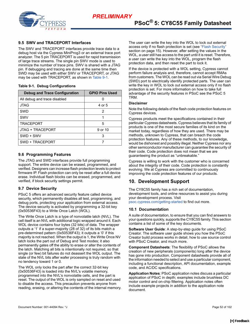
PRELIMINARYPSoC® 5: CY8C55 Family Datasheet
Document Number: 001-44094 Rev. *J Page 52 of 102
9.5 SWV and TRACEPORT Interfaces
The SWV and TRACEPORT interfaces provide trace data to a debug host via the Cypress MiniProg3 or an external trace port analyzer. The 5 pin TRACEPORT is used for rapid transmission of large trace streams. The single pin SWV mode is used to minimize the number of trace pins. SWV is shared with a JTAG pin. If debugging and tracing are done at the same time then SWD may be used with either SWV or TRACEPORT, or JTAG may be used with TRACEPORT, as shown in Table 9-1.
9.6 Programming Features
The JTAG and SWD interfaces provide full programming support. The entire device can be erased, programmed, and verified. Designers can increase flash protection levels to protect firmware IP. Flash protection can only be reset after a full device erase. Individual flash blocks can be erased, programmed, and verified, if block security settings permit.
9.7 Device Security
PSoC 5 offers an advanced security feature called device security, which permanently disables all test, programming, and debug ports, protecting your application from external access. The device security is activated by programming a 32-bit key (0x50536F43) to a Write Once Latch (WOL).
The Write Once Latch is a type of nonvolatile latch (NVL). The cell itself is an NVL with additional logic wrapped around it. Each WOL device contains four bytes (32 bits) of data. The wrapper outputs a ‘1’ if a super-majority (28 of 32) of its bits match a pre-determined pattern (0x50536F43); it outputs a ‘0’ if this majority is not reached. When the output is 1, the Write Once NV latch locks the part out of Debug and Test modes; it also permanently gates off the ability to erase or alter the contents of the latch. Matching all bits is intentionally not required, so that single (or few) bit failures do not deassert the WOL output. The state of the NVL bits after wafer processing is truly random with no tendency toward 1 or 0.
The WOL only locks the part after the correct 32-bit key (0x50536F43) is loaded into the NVL's volatile memory, programmed into the NVL's nonvolatile cells, and the part is reset. The output of the WOL is only sampled on reset and used to disable the access. This precaution prevents anyone from reading, erasing, or altering the contents of the internal memory.
The user can write the key into the WOL to lock out external access only if no flash protection is set (see “Flash Security” section on page 15). However, after setting the values in the WOL, a user still has access to the part until it is reset. Therefore, a user can write the key into the WOL, program the flash protection data, and then reset the part to lock it.
If the device is protected with a WOL setting, Cypress cannot perform failure analysis and, therefore, cannot accept RMAs from customers. The WOL can be read out via Serial Wire Debug (SWD) port to electrically identify protected parts. The user can write the key in WOL to lock out external access only if no flash protection is set. For more information on how to take full advantage of the security features in PSoC see the PSoC 5 TRM.
Disclaimer
Note the following details of the flash code protection features on Cypress devices.
Cypress products meet the specifications contained in their particular Cypress datasheets. Cypress believes that its family of products is one of the most secure families of its kind on the market today, regardless of how they are used. There may be methods, unknown to Cypress, that can breach the code protection features. Any of these methods, to our knowledge, would be dishonest and possibly illegal. Neither Cypress nor any other semiconductor manufacturer can guarantee the security of their code. Code protection does not mean that we are guaranteeing the product as “unbreakable.”
Cypress is willing to work with the customer who is concerned about the integrity of their code. Code protection is constantly evolving. We at Cypress are committed to continuously improving the code protection features of our products.
10. Development Support
The CY8C55 family has a rich set of documentation, development tools, and online resources to assist you during your development process. Visit psoc.cypress.com/getting-started to find out more.
10.1 Documentation
A suite of documentation, to ensure that you can find answers to your questions quickly, supports the CY8C55 family. This section contains a list of some of the key documents.
Software User Guide: A step-by-step guide for using PSoC Creator. The software user guide shows you how the PSoC Creator build process works in detail, how to use source control with PSoC Creator, and much more.
Component Datasheets: The flexibility of PSoC allows the creation of new peripherals (components) long after the device has gone into production. Component datasheets provide all of the information needed to select and use a particular component, including a functional description, API documentation, example code, and AC/DC specifications.
Application Notes: PSoC application notes discuss a particular application of PSoC in depth; examples include brushless DC motor control and on-chip filtering. Application notes often include example projects in addition to the application note document.
Table 9-1. Debug Configurations
Debug and Trace Configuration GPIO Pins Used
All debug and trace disabled 0
JTAG 4 or 5
SWD 2
SWV 1
TRACEPORT 5
JTAG + TRACEPORT 9 or 10
SWD + SWV 3
SWD + TRACEPORT 7
[+] Feedback [+] Feedback [+] Feedback [+] Feedback

PRELIMINARYPSoC® 5: CY8C55 Family Datasheet
Document Number: 001-44094 Rev. *J Page 53 of 102
Technical Reference Manual: PSoC Creator makes designing with PSoC as easy as dragging a peripheral onto a schematic, but, when low level details of the PSoC device are required, use the technical reference manual (TRM) as your guide.
Note Visit www.arm.com for detailed documentation about the Cortex-M3 CPU.
10.2 Online
In addition to print documentation, the Cypress PSoC forums connect you with fellow PSoC users and experts in PSoC from around the world, 24 hours a day, 7 days a week.
10.3 Tools
With industry standard cores, programming, and debugging interfaces, the CY8C55 family is part of a development tool ecosystem. Visit us at www.cypress.com/go/psoccreator for the latest information on the revolutionary, easy to use PSoC Creator IDE, supported third party compilers, programmers, debuggers, and development kits.
[+] Feedback [+] Feedback [+] Feedback [+] Feedback

PRELIMINARYPSoC® 5: CY8C55 Family Datasheet
Document Number: 001-44094 Rev. *J Page 54 of 102
11. Electrical Specifications
Specifications are valid for -40 °C TA 85 °C and TJ 100 °C, except where noted. Specifications are valid for 1.71 V to 5.5 V, except where noted. The unique flexibility of the PSoC UDBs and analog blocks enable many functions to be implemented in PSoC Creator components, see the component datasheets for full AC/DC specifications of individual functions. See the “Example Peripherals” section on page 31 for further explanation of PSoC Creator components.
11.1 Absolute Maximum Ratings
Note Usage above the absolute maximum conditions listed in Table 11-1 may cause permanent damage to the device. Exposure to maximum conditions for extended periods of time may affect device reliability. When used below maximum conditions but above normal operating conditions the device may not operate to specification.
Table 11-1. Absolute Maximum Ratings DC Specifications
Parameter Description Conditions Min Typ Max Units
TSTG Storage temperature Higher storage temperatures reduce NVL data retention time. Recommended storage temper-ature is +25 °C ±25 °C. Extended duration storage temperatures above 85 °C degrade reliability.
–55 25 100 °C
VDDA Analog supply voltage relative to VSSA
–0.5 – 6 V
VDDD Digital supply voltage relative to VSSD
–0.5 – 6 V
VDDIO I/O supply voltage relative to VSSD –0.5 – 6 V
VCCA Direct analog core voltage input –0.5 – 1.95 V
VCCD Direct digital core voltage input –0.5 – 1.95 V
VSSA Analog ground voltage VSSD – 0.5 – VSSD + 0.5
V
VGPIO[12] DC input voltage on GPIO Includes signals sourced by VDDA
and routed internal to the pin.VSSD – 0.5 – VDDIO +
0.5V
VSIO DC input voltage on SIO Output disabled VSSD – 0.5 – 7 V
Output enabled VSSD – 0.5 – 6 V
VIND Voltage at boost converter input 0.5 – 5.5 V
VBAT Boost converter supply VSSD – 0.5 – 5.5 V
Ivddio Current per VDDIO supply pin – – 100 mA
ESDHBM Electrostatic discharge voltage Human body model 2200 – – V
ESDCDM ESD voltage Charge device model 500 – – V
Note12. The VDDIO supply voltage must be greater than the maximum analog voltage on the associated GPIO pins. Maximum analog voltage on GPIO pin VDDIO VDDA.
[+] Feedback [+] Feedback [+] Feedback [+] Feedback
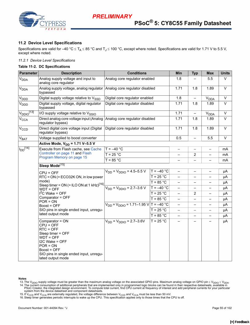
PRELIMINARYPSoC® 5: CY8C55 Family Datasheet
Document Number: 001-44094 Rev. *J Page 55 of 102
11.2 Device Level Specifications
Specifications are valid for –40 °C TA 85 °C and TJ 100 °C, except where noted. Specifications are valid for 1.71 V to 5.5 V, except where noted.
11.2.1 Device Level Specifications
Table 11-2. DC Specifications
Parameter Description Conditions Min Typ Max Units
VDDA Analog supply voltage and input to analog core regulator
Analog core regulator enabled 1.8 – 5.5 V
VDDA Analog supply voltage, analog regulator bypassed
Analog core regulator disabled 1.71 1.8 1.89 V
VDDD Digital supply voltage relative to VSSD Digital core regulator enabled 1.8 – VDDA V
VDDD Digital supply voltage, digital regulator bypassed
Digital core regulator disabled 1.71 1.8 1.89 V
VDDIO[13] I/O supply voltage relative to VSSIO 1.71 – VDDA V
VCCA Direct analog core voltage input (Analog regulator bypass)
Analog core regulator disabled 1.71 1.8 1.89 V
VCCD Direct digital core voltage input (Digital regulator bypass)
Digital core regulator disabled 1.71 1.8 1.89 V
VBAT Voltage supplied to boost converter 0.5 – 5.5 V
Active Mode, VDD = 1.71 V–5.5 V
IDD[14] Execute from Flash cache, see Cache
Controller on page 11 and Flash Program Memory on page 15
T = –40 °C – – – mA
T = 25 °C – 2 – mA
T = 85 °C – – – mA
Sleep Mode[15]
CPU = OFFRTC = ON (= ECO32K ON, in low power mode)Sleep timer = ON (= ILO ON at 1 kHz)[16]
WDT = OFFI2C Wake = OFFComparator = OFFPOR = ONBoost = OFFSIO pins in single ended input, unregu-lated output mode
VDD = VDDIO = 4.5–5.5 V T = –40 °C – – – µA
T = 25 °C – – – µA
T = 85 °C – – – µA
VDD = VDDIO = 2.7–3.6 V T = –40 °C – – – µA
T = 25 °C – 2 – µA
T = 85 °C – – – µA
VDD = VDDIO = 1.71–1.95 V T = –40 °C – – – µA
T = 25 °C – – – µA
T = 85 °C – – – µA
Comparator = ONCPU = OFFRTC = OFFSleep timer = OFFWDT = OFFI2C Wake = OFFPOR = ONBoost = OFFSIO pins in single ended input, unregu-lated output mode
VDD = VDDIO = 2.7–3.6V T = 25 °C – – – µA
Notes13. The VDDIO supply voltage must be greater than the maximum analog voltage on the associated GPIO pins. Maximum analog voltage on GPIO pin VDDIO VDDA.14. The current consumption of additional peripherals that are implemented only in programmed logic blocks can be found in their respective datasheets, available in
PSoC Creator, the integrated design environment. To compute total current, find CPU current at frequency of interest and add peripheral currents for your particular system from the device datasheet and component datasheets.
15. If VCCD and VCCA are externally regulated, the voltage difference between VCCD and VCCA must be less than 50 mV.16. Sleep timer generates periodic interrupts to wake up the CPU. This specification applies only to those times that the CPU is off.
[+] Feedback [+] Feedback [+] Feedback [+] Feedback

PRELIMINARYPSoC® 5: CY8C55 Family Datasheet
Document Number: 001-44094 Rev. *J Page 56 of 102
I2C Wake = ONCPU = OFFRTC = OFFSleep timer = OFFWDT = OFFComparator = OFFPOR = ONBoost = OFFSIO pins in single ended input, unregu-lated output mode
VDD = VDDIO = 2.7–3.6V T = 25 °C – – – µA
Hibernate Mode[17]
Hibernate mode currentAll regulators and oscillators off.SRAM retentionGPIO interrupts are activeBoost = OFFSIO pins in single ended input, unregu-lated output mode
VDD = VDDIO = 4.5–5.5 V T = –40 °C – – – nA
T = 25 °C – – – nA
T = 85 °C – – – nA
VDD = VDDIO = 2.7 – 3.6 V T = –40 °C – – – nA
T = 25 °C – 300 – nA
T = 85 °C – – – nA
VDD = VDDIO = 1.71–1.95 V T = –40 °C – – – nA
T = 25 °C – – – nA
T = 85 °C – – – nA
Table 11-2. DC Specifications (continued)
Parameter Description Conditions Min Typ Max Units
Notes17. If VCCD and VCCA are externally regulated, the voltage difference between VCCD and VCCA must be less than 50 mV.18. Based on device characterization (Not production tested).
Table 11-3. AC Specifications[18]
Parameter Description Conditions Min Typ Max Units
FCPU CPU frequency 1.71 V VDDD 5.5 V DC – 80 MHz
FBUSCLK Bus frequency 1.71 V VDDD 5.5 V DC – 80 MHz
Svdd VDD ramp rate – – 1 V/ns
TIO_INIT Time from VDDD/VDDA/VCCD/VCCA IPOR to I/O ports set to their reset states
– – 10 µs
TSTARTUP Time from VDDD/VDDA/VCCD/VCCA PRES to CPU executing code at reset vector
VCCA/VDDA = regulated from VDDA/VDDD, no PLL used, fast IMO boot mode (48 MHz typ.)
– – 33 µs
VCCA/VCCD = regulated from VDDA/VDDD, no PLL used, slow IMO boot mode (12 MHz typ.)
– – 66 µs
TSLEEP Wakeup from limited active mode – Application of non-LVD interrupt to beginning of execution of next CPU instruction
– – 12 µs
Wakeup from sleep mode – Occur-rence of LVD interrupt to beginning of execution of next CPU instruction
– – 15 µs
THIBERNATE Wakeup form hibernate mode – Application of external interrupt to beginning of execution of next CPU instruction
– – 100 µs
[+] Feedback [+] Feedback [+] Feedback [+] Feedback
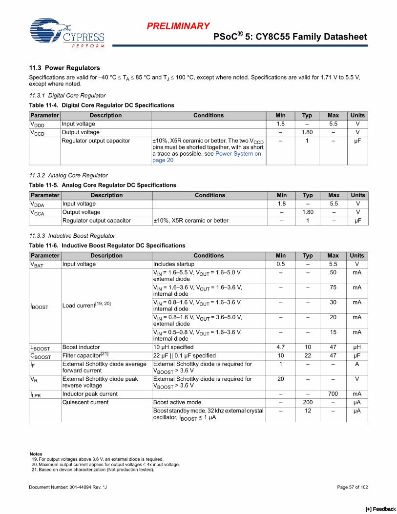
PRELIMINARYPSoC® 5: CY8C55 Family Datasheet
Document Number: 001-44094 Rev. *J Page 57 of 102
11.3 Power Regulators
Specifications are valid for –40 °C TA 85 °C and TJ 100 °C, except where noted. Specifications are valid for 1.71 V to 5.5 V, except where noted.
11.3.1 Digital Core Regulator
11.3.2 Analog Core Regulator
11.3.3 Inductive Boost Regulator
Table 11-4. Digital Core Regulator DC Specifications
Parameter Description Conditions Min Typ Max Units
VDDD Input voltage 1.8 – 5.5 V
VCCD Output voltage – 1.80 – V
Regulator output capacitor ±10%, X5R ceramic or better. The two VCCD pins must be shorted together, with as short a trace as possible, see Power System on page 20
– 1 – µF
Table 11-5. Analog Core Regulator DC Specifications
Parameter Description Conditions Min Typ Max Units
VDDA Input voltage 1.8 – 5.5 V
VCCA Output voltage – 1.80 – V
Regulator output capacitor ±10%, X5R ceramic or better – 1 – µF
Table 11-6. Inductive Boost Regulator DC Specifications
Parameter Description Conditions Min Typ Max Units
VBAT Input voltage Includes startup 0.5 – 5.5 V
IBOOST Load current[19, 20]
VIN = 1.6–5.5 V, VOUT = 1.6–5.0 V, external diode
– – 50 mA
VIN = 1.6–3.6 V, VOUT = 1.6–3.6 V,internal diode
– – 75 mA
VIN = 0.8–1.6 V, VOUT = 1.6–3.6 V, internal diode
– – 30 mA
VIN = 0.8–1.6 V, VOUT = 3.6–5.0 V, external diode
– – 20 mA
VIN = 0.5–0.8 V, VOUT = 1.6–3.6 V, internal diode
– – 15 mA
LBOOST Boost inductor 10 µH specified 4.7 10 47 µH
CBOOST Filter capacitor[21] 22 µF || 0.1 µF specified 10 22 47 µF
IF External Schottky diode average forward current
External Schottky diode is required for VBOOST > 3.6 V
1 – – A
VR External Schottky diode peak reverse voltage
External Schottky diode is required for VBOOST > 3.6 V
20 – – V
ILPK Inductor peak current – – 700 mA
Quiescent current Boost active mode – 200 – µA
Boost standby mode, 32 khz external crystal oscillator, IBOOST < 1 µA
– 12 – µA
Notes19. For output voltages above 3.6 V, an external diode is required.20. Maximum output current applies for output voltages 4x input voltage.21. Based on device characterization (Not production tested).
[+] Feedback [+] Feedback [+] Feedback [+] Feedback

PRELIMINARYPSoC® 5: CY8C55 Family Datasheet
Document Number: 001-44094 Rev. *J Page 58 of 102
11.4 Inputs and Outputs
Specifications are valid for –40 °C TA 85 °C and TJ 100 °C, except where noted. Specifications are valid for 1.71 V to 5.5 V, except where noted.
11.4.1 GPIO
VBOOST
Boost output voltage range[22]
1.8 V 1.71 1.80 1.89 V
1.9 V 1.81 1.90 2.00 V
2.0 V 1.90 2.00 2.10 V
2.4 V 2.28 2.40 2.52 V
2.7 V 2.57 2.70 2.84 V
3.0 V 2.85 3.00 3.15 V
3.3 V 3.14 3.30 3.47 V
3.6 V 3.42 3.60 3.8 V
5.0 V External diode required 4.75 5.00 5.25 V
Load regulation – – TBD %
Line regulation – – TBD %
Efficiency VBAT = 2.4 V, VOUT = 2.7 V, IOUT = 10 mA, Fsw = 400 kHz
90 – – %
Table 11-6. Inductive Boost Regulator DC Specifications (continued)
Parameter Description Conditions Min Typ Max Units
Note22. Based on device characterization (Not production tested).
Table 11-7. Inductive Boost Regulator AC Specifications
Parameter Description Conditions Min Typ Max Units
VRIPPLE Ripple voltage (peak-to-peak) VOUT = 1.8 V, FSW = 400 kHz, IOUT = 10 mA – – 100 mV
FSW Switching frequency – 0.1, 0.4, or 2
– MHz
Duty cycle 20 – 80 %
Table 11-8. GPIO DC Specifications
Parameter Description Conditions Min Typ Max Units
VIH Input voltage high threshold CMOS Input, PRT[x]CTL = 0 0.7 VDDIO – – V
VIL Input voltage low threshold CMOS Input, PRT[x]CTL = 0 – – 0.3 VDDIO
V
VIH Input voltage high threshold LVTTL Input, PRT[x]CTL = 1,VDDIO < 2.7 V
0.7 x VDDIO – – V
VIH Input voltage high threshold LVTTL Input, PRT[x]CTL = 1, VDDIO 2.7 V
2.0 – – V
VIL Input voltage low threshold LVTTL Input, PRT[x]CTL = 1,VDDIO < 2.7 V
– – 0.3 x VDDIO
V
VIL Input voltage low threshold LVTTL Input, PRT[x]CTL = 1, VDDIO 2.7 V
– – 0.8 V
VOH Output voltage high IOH = 4 mA at 3.3 VDDIO VDDIO – 0.6 – – V
IOH = 1 mA at 1.8 VDDIO VDDIO – 0.5 – – V
VOL Output voltage low IOL = 8 mA at 3.3 VDDIO – – 0.6 V
IOL = 4 mA at 1.8 VDDIO – – 0.6 V
[+] Feedback [+] Feedback [+] Feedback [+] Feedback

PRELIMINARYPSoC® 5: CY8C55 Family Datasheet
Document Number: 001-44094 Rev. *J Page 59 of 102
Rpullup Pull-up resistor 4 5.6 8 k
Rpulldown Pull-down resistor 4 5.6 8 kIIL Input leakage current (absolute
value)[23]25 °C, VDDIO = 3.0 V – – 2 nA
CIN Input capacitance[23] GPIOs without opamp outputs – – 7 pF
GPIOs with opamp outputs – – 18 pF
VH Input voltage hysteresis (Schmitt-Trigger)[23]
– 40 – mV
Idiode Current through protection diode to VDDIO and VSSIO
– – 100 µA
Rglobal Resistance pin to analog global bus 25 °C, VDDIO = 3.0 V – 320 – Rmux Resistance pin to analog mux bus 25 °C, VDDIO = 3.0 V – 220 –
Table 11-8. GPIO DC Specifications (continued)
Parameter Description Conditions Min Typ Max Units
Note23. Based on device characterization (Not production tested).
Table 11-9. GPIO AC Specifications
Parameter Description Conditions Min Typ Max Units
TriseF Rise time in Fast Strong Mode[23] 3.3 V VDDIO Cload = 25 pF 2 – 12 ns
TfallF Fall time in Fast Strong Mode[23] 3.3 V VDDIO Cload = 25 pF 2 – 12 ns
TriseS Rise time in Slow Strong Mode[23] 3.3 V VDDIO Cload = 25 pF 10 – 60 ns
TfallS Fall time in Slow Strong Mode[23] 3.3 V VDDIO Cload = 25 pF 10 – 60 ns
Fgpioout
GPIO output operating frequency
3.3 V < VDDIO < 5.5 V, fast strong drive mode
90/10% VDDIO into 25 pF – – 33 MHz
1.71 V < VDDIO < 3.3 V, fast strong drive mode
90/10% VDDIO into 25 pF – – 20 MHz
3.3 V < VDDIO < 5.5 V, slow strong drive mode
90/10% VDDIO into 25 pF – – 7 MHz
1.71 V < VDDIO < 3.3 V, slow strong drive mode
90/10% VDDIO into 25 pF – – 3.5 MHz
FgpioinGPIO input operating frequency
1.71 V < VDDIO < 5.5 V 90/10% VDDIO – – 66 MHz
[+] Feedback [+] Feedback [+] Feedback [+] Feedback

PRELIMINARYPSoC® 5: CY8C55 Family Datasheet
Document Number: 001-44094 Rev. *J Page 60 of 102
11.4.2 SIO
Table 11-10. SIO DC Specifications
Parameter Description Conditions Min Typ Max Units
Vinref Input voltage reference (differential input mode)
0.5 – 0.52 VDDIO V
Voutref
Output voltage reference (regulated output mode)
VDDIO > 3.7 1 – VDDIO – 1 V
VDDIO < 3.7 1 – VDDIO – 0.5 V
VIH
Input voltage high threshold
GPIO mode CMOS input 0.7 VDDIO – – V
Differential input mode Hysteresis disabled Vinref + 0.1 – – V
VIL
Input voltage low threshold
GPIO mode CMOS input – – 0.3 VDDIO V
Differential input mode Hysteresis disabled – – Vinref – 0.1 V
VOH
Output voltage high
Unregulated mode IOH = 4 mA, VDDIO = 3.3 V VDDIO – 0.4 – – V
Regulated mode IOH = 1 mA Voutref – 0.6 – Voutref + 0.2 V
Regulated mode IOH = 0.1 mA Voutref – 0.25 – Voutref + 0.2 V
VOL
Output voltage low
VDDIO = 3.30 V, IOL = 25 mA – – 0.8 V
VDDIO = 1.80 V, IOL = 4 mA – – 0.4 V
Rpullup Pull-up resistor 4 5.6 8 kRpulldown Pull-down resistor 4 5.6 8 kIIL Input leakage current (absolute
value)[24]
VIH < Vddsio 25 °C, Vddsio = 3.0 V, VIH = 3.0 V – – 14 nA
VIH > Vddsio 25 °C, Vddsio = 0 V, VIH = 3.0 V – – 10 µA
CIN Input Capacitance[24] – – 7 pF
VHInput voltage hysteresis (Schmitt-Trigger)[24]
Single ended mode (GPIO mode) – 40 – mV
Differential mode – 50 – mV
Idiode Current through protection diode to VSSIO
– – 100 µA
Table 11-11. SIO AC Specifications
Parameter Description Conditions Min Typ Max Units
TriseF Rise time in fast strong mode (90/10%)[24]
Cload = 25 pF, VDDIO = 3.3 V 1 – 12 ns
TfallF Fall time in fast strong mode (90/10%)[24]
Cload = 25 pF, VDDIO = 3.3 V 1 – 12 ns
TriseS Rise time in slow strong mode (90/10%)[24]
Cload = 25 pF, VDDIO = 3.0 V 10 – 75 ns
TfallS Fall time in slow strong mode (90/10%)[24]
Cload = 25 pF, VDDIO = 3.0 V 10 – 60 ns
Note24. Based on device characterization (Not production tested).
[+] Feedback [+] Feedback [+] Feedback [+] Feedback

PRELIMINARYPSoC® 5: CY8C55 Family Datasheet
Document Number: 001-44094 Rev. *J Page 61 of 102
11.4.3 USBIO
For operation in USB mode, VDDD range condition is 3.15 V VDDD 3.45 V (USB regulator bypassed) or 4.35 V VDDD 5.25 V (USB regulator in use). For operation in GPIO mode, the standard range for VDDD applies, see Device Level Specifications on page 55.
Fsioout
SIO output operating frequency
3.3 V < VDDIO < 5.5 V, Unregulated output (GPIO) mode, fast strong drive mode
90/10% VDDIO into 25 pF – – 33 MHz
1.71 V < VDDIO < 3.3 V, Unregu-lated output (GPIO) mode, fast strong drive mode
90/10% VDDIO into 25 pF – – 16 MHz
3.3 V < VDDIO < 5.5 V, Unregulated output (GPIO) mode, slow strong drive mode
90/10% VDDIO into 25 pF – – 5 MHz
1.71 V < VDDIO < 3.3 V, Unregu-lated output (GPIO) mode, slow strong drive mode
90/10% VDDIO into 25 pF – – 4 MHz
3.3 V < VDDIO < 5.5 V, Regulated output mode, fast strong drive mode
Output continuously switching into 25 pF
– – 20 MHz
1.71 V < VDDIO < 3.3 V, Regulated output mode, fast strong drive mode
Output continuously switching into 25 pF
– – 10 MHz
1.71 V < VDDIO < 5.5 V, Regulated output mode, slow strong drive mode
Output continuously switching into 25 pF
– – 2.5 MHz
FsioinSIO input operating frequency
1.71 V < VDDIO < 5.5 V 90/10% VDDIO – – 66 MHz
Table 11-12. USBIO DC Specifications
Parameter Description Conditions Min Typ Max Units
Rusbi USB D+ pull-up resistance With idle bus 0.900 – 1.575 k
Rusba USB D+ pull-up resistance While receiving traffic 1.425 – 3.090 k
Vohusb Static output high 15 k ±5% to Vss, internal pull-up enabled
2.8 – 3.6 V
Volusb Static output low 15 k ±5% to Vss, internal pull-up enabled
– – 0.3 V
Vohgpio Output voltage high, GPIO mode IOH = 4 mA, VDDD 3 V 2.4 – – V
Volgpio Output voltage low, GPIO mode IOL = 4 mA, VDDD 3 V – – 0.3 V
Vdi Differential input sensitivity |(D+)–(D–)| – – 0.2 V
Vcm Differential input common mode range 0.8 – 2.5 V
Vse Single ended receiver threshold 0.8 – 2 V
Rps2 PS/2 pull-up resistance In PS/2 mode, with PS/2 pull-up enabled
3 – 7 k
Rext External USB series resistor In series with each USB pin 21.78 (–1%)
22 22.22 (+1%)
Zo USB driver output impedance Including Rext 28 – 44
CIN USB transceiver input capacitance – – 20 pF
IIL Input leakage current (absolute value) 25 °C, VDDD = 3.0 V – – 2 nA
Table 11-11. SIO AC Specifications (continued)
Parameter Description Conditions Min Typ Max Units
[+] Feedback [+] Feedback [+] Feedback [+] Feedback

PRELIMINARYPSoC® 5: CY8C55 Family Datasheet
Document Number: 001-44094 Rev. *J Page 62 of 102
11.4.4 XRES
Table 11-13. USBIO AC Specifications
Parameter Description Conditions Min Typ Max Units
Tdrate Full-speed data rate average bit rate 12 – 0.25% 12 12 + 0.25%
MHz
Tjr1 Receiver data jitter tolerance to next transition
–8 – 8 ns
Tjr2 Receiver data jitter tolerance to pair transition
–5 – 5 ns
Tdj1 Driver differential jitter to next transition –3.5 – 3.5 ns
Tdj2 Driver differential jitter to pair transition –4 – 4 ns
Tfdeop Source jitter for differential transition to SE0 transition
–2 – 5 ns
Tfeopt Source SE0 interval of EOP 160 – 175 ns
Tfeopr Receiver SE0 interval of EOP 82 – – ns
Tfst Width of SE0 interval during differential transition
– – 14 ns
Fgpio_out GPIO mode output operating frequency 3 V VDDD 5.5 V – – 20 MHz
VDDD = 1.71 V – – 6 MHz
Tr_gpio Rise time, GPIO mode, 10%/90% VDDD VDDD > 3 V, 25 pF load 1 – 12 ns
VDDD = 1.71 V, 25 pF load 4 – 40 ns
Tf_gpio Fall time, GPIO mode, 90%/10% VDDD VDDD > 3 V, 25 pF load 1 – 12 ns
VDDD = 1.71 V, 25 pF load 4 – 40 ns
Table 11-14. USB Driver AC Specifications
Parameter Description Conditions Min Typ Max Units
Tr Transition rise time 4 – 20 ns
Tf Transition fall time 4 – 20 ns
TR Rise/fall time matching 90% – 111%
Vcrs Output signal crossover voltage 1.3 – 2 V
Note25. Based on device characterization (Not production tested).
Table 11-15. XRES DC Specifications
Parameter Description Conditions Min Typ Max Units
VIH Input voltage high threshold CMOS Input, PRT[x]CTL = 0 0.7 VDDIO – – V
VIL Input voltage low threshold CMOS Input, PRT[x]CTL = 0 – – 0.3 VDDIO V
Rpullup Pull-up resistor 4 5.6 8 k
CIN Input capacitance[25] – 3 pF
VH Input voltage hysteresis (Schmitt-Trigger)[25]
– 100 – mV
Idiode Current through protection diode to VDDIO and VSSIO
– – 100 µA
Table 11-16. XRES AC Specifications
Parameter Description Conditions Min Typ Max Units
TRESET Reset pulse width 1 – – µs
[+] Feedback [+] Feedback [+] Feedback [+] Feedback
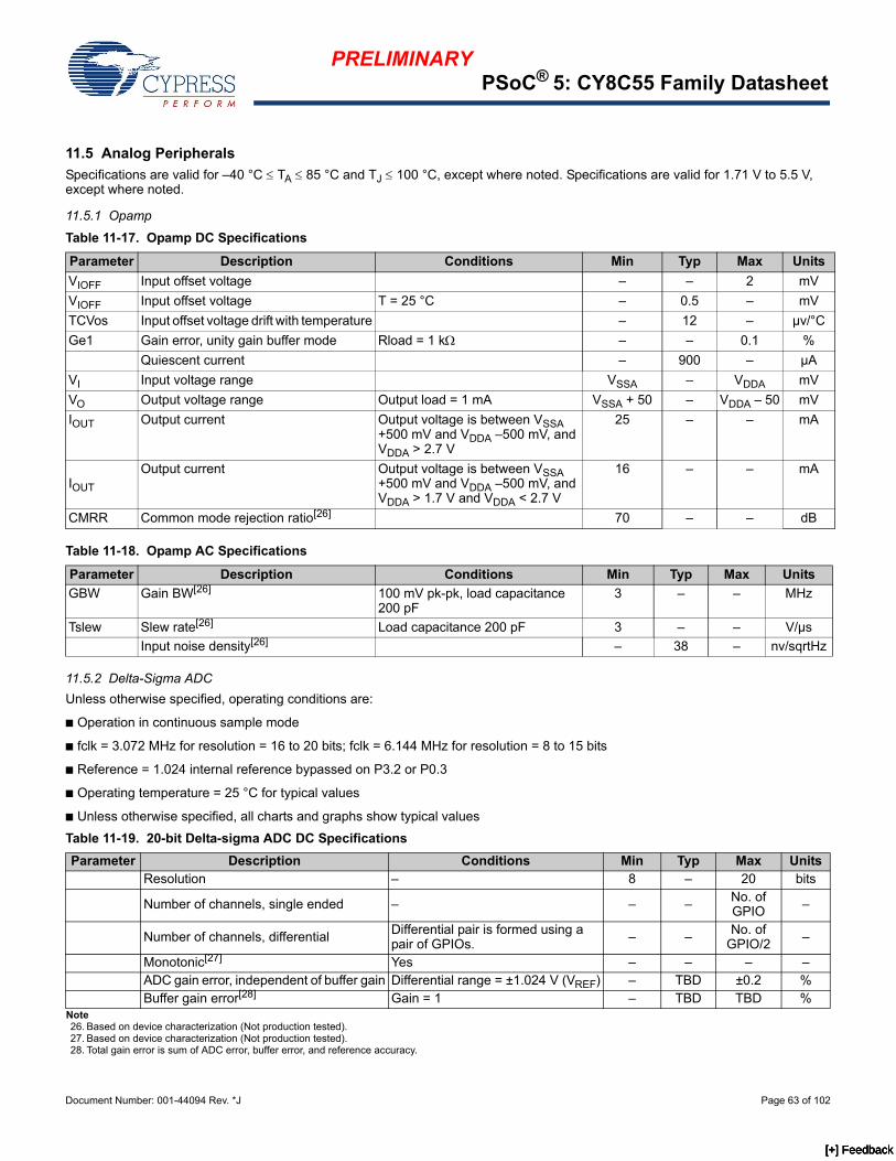
PRELIMINARYPSoC® 5: CY8C55 Family Datasheet
Document Number: 001-44094 Rev. *J Page 63 of 102
11.5 Analog Peripherals
Specifications are valid for –40 °C TA 85 °C and TJ 100 °C, except where noted. Specifications are valid for 1.71 V to 5.5 V, except where noted.
11.5.1 Opamp
11.5.2 Delta-Sigma ADC
Unless otherwise specified, operating conditions are:
■ Operation in continuous sample mode
■ fclk = 3.072 MHz for resolution = 16 to 20 bits; fclk = 6.144 MHz for resolution = 8 to 15 bits
■ Reference = 1.024 internal reference bypassed on P3.2 or P0.3
■ Operating temperature = 25 °C for typical values
■ Unless otherwise specified, all charts and graphs show typical values
Table 11-17. Opamp DC Specifications
Parameter Description Conditions Min Typ Max Units
VIOFF Input offset voltage – – 2 mV
VIOFF Input offset voltage T = 25 °C – 0.5 – mV
TCVos Input offset voltage drift with temperature – 12 – µv/°C
Ge1 Gain error, unity gain buffer mode Rload = 1 k – – 0.1 %
Quiescent current – 900 – µA
VI Input voltage range VSSA – VDDA mV
VO Output voltage range Output load = 1 mA VSSA + 50 – VDDA – 50 mV
IOUT Output current Output voltage is between VSSA +500 mV and VDDA –500 mV, and VDDA > 2.7 V
25 – – mA
IOUT
Output current Output voltage is between VSSA +500 mV and VDDA –500 mV, and VDDA > 1.7 V and VDDA < 2.7 V
16 – – mA
CMRR Common mode rejection ratio[26] 70 – – dB
Table 11-18. Opamp AC Specifications
Parameter Description Conditions Min Typ Max Units
GBW Gain BW[26] 100 mV pk-pk, load capacitance 200 pF
3 – – MHz
Tslew Slew rate[26] Load capacitance 200 pF 3 – – V/µs
Input noise density[26] – 38 – nv/sqrtHz
Note26. Based on device characterization (Not production tested).27. Based on device characterization (Not production tested).28. Total gain error is sum of ADC error, buffer error, and reference accuracy.
Table 11-19. 20-bit Delta-sigma ADC DC Specifications
Parameter Description Conditions Min Typ Max UnitsResolution – 8 – 20 bits
Number of channels, single ended – – – No. of GPIO –
Number of channels, differentialDifferential pair is formed using a pair of GPIOs. – –
No. of GPIO/2 –
Monotonic[27] Yes – – – –ADC gain error, independent of buffer gain Differential range = ±1.024 V (VREF) – TBD ±0.2 %Buffer gain error[28] Gain = 1 – TBD TBD %
[+] Feedback [+] Feedback [+] Feedback [+] Feedback

PRELIMINARYPSoC® 5: CY8C55 Family Datasheet
Document Number: 001-44094 Rev. *J Page 64 of 102
Temperature coefficient of input gain error
Unbuffered, differential range = ±1.024 V (VREF) – TBD TBD µV/°C
Buffered, buffer gain = 1, differential range = ±1.024 V (VREF) – TBD TBD µV/°C
Vos_ADC ADC input offset voltage – – TBD ±0.1 mVVos_Buf Buffer input offset voltage[31] – – TBD TBD mVTCVos_ADC ADC TC input offset voltage – – TBD TBD µV/°CTCVos_Buf Buffer TC input offset voltage – – TBD TBD µV/°C
Input voltage range, single ended[29] – VSSA – VDDA VInput voltage range, differential unbuf-fered[29] – VSSA – VDDA V
Input voltage range, differential, buffered[29] – VSSA – VDDA – 1 V
PSRRb Power supply rejection ratio, buffered[29] Buffer gain = 1, 16-bit, Range = ±1.024 V 90 – – dB
CMRRb Common mode rejection ratio, buffered[29] Buffer gain = 1, 16 bit, Range = ±1.024 V 90 – – dB
INL20 Integral non linearity[29] Range = ±1.024 V, unbuffered – TBD ±32 LSBDNL20 Differential non linearity[29] Range = ±1.024 V, unbuffered – TBD ±1 LSBINL16 Integral non linearity[29] Range = ±1.024 V, unbuffered – TBD ±2 LSBDNL16 Differential non linearity[29] Range = ±1.024 V, unbuffered – TBD ±1 LSBINL12 Integral non linearity[29] Range = ±1.024 V, unbuffered – TBD ±1 LSBDNL12 Differential non linearity[29] Range = ±1.024 V, unbuffered – TBD ±1 LSBINL8 Integral non linearity[29] Range = ±1.024 V, unbuffered – TBD TBD LSBDNL8 Differential non linearity[29] Range = ±1.024 V, unbuffered – TBD TBD LSBRin_Buff ADC input resistance Input buffer used 10 – – M
Rin_ADC16 ADC input resistance[29] Input buffer bypassed, 16-bit, Range = ±1.024 V
– 74[32] – k
Rin_ADC12 ADC input resistance[29] Input buffer bypassed, 12 bit, Range = ±1.024 V – 148[32] – k
Cin_G1 ADC input capacitance[29] Gain = 1 – 5 – pF
VextrefADC external reference input voltage, see also internal reference in Voltage Reference on page 69
Pins P0[3], P3[2] TBD – TBD V
Current ConsumptionIDD_20 Current consumption, 20 bit[29] 187 sps, unbuffered – TBD TBD mAIDD_16 Current consumption, 16 bit[29] 48 ksps, unbuffered – TBD TBD mAIDD_12 Current consumption, 12 bit[29] 192 ksps, unbuffered – TBD TBD mAIDD_8 Current consumption, 8 bit[29] 384 ksps, unbuffered – TBD TBD mAIBUFF Buffer current consumption[29] – – TBD TBD mA
Table 11-19. 20-bit Delta-sigma ADC DC Specifications (continued)
Parameter Description Conditions Min Typ Max Units
Notes29. Based on device characterization (not production tested).30. Total gain error is sum of ADC error, buffer error, and reference accuracy.31. Total offset voltage error is sum of buffer Vos and ADC Vos32. By using switched capacitors at the ADC input an effective input resistance is created. Holding the gain and number of bits constant, the resistance is proportional
to the inverse of the clock frequency. For more information see the Technical Reference Manual.
[+] Feedback [+] Feedback [+] Feedback [+] Feedback

PRELIMINARYPSoC® 5: CY8C55 Family Datasheet
Document Number: 001-44094 Rev. *J Page 65 of 102
Table 11-20. Delta-sigma ADC AC SpecificationsParameter Description Conditions Min Typ Max Units
Startup time – – – 4 Samples
THD Total harmonic distortion[33] Buffer gain = 1, 16 bit, Range = ±1.024 V
– TBD 0.0032 %
20-Bit Resolution Mode
SR20 Sample rate[33] Range = ±1.024 V, unbuffered 7.8 – 187 sps
BW20 Input bandwidth at max sample rate[33] Range = ±1.024V, unbuffered – 40 – Hz
SNR20int Signal to noise ratio, 20-bit, external reference[33]
Range = ±1.024V, unbuffered TBD TBD – dB
SNR20ext Signal to noise ratio, 20-bit, external reference[33]
Range = ±1.024V, unbuffered 110 TBD – dB
16-Bit Resolution Mode
SR16 Sample rate[33] Range = ±1.024 V, unbuffered 2 – 48 ksps
BW16 Input bandwidth at max sample rate[33] Range = ±1.024 V, unbuffered – 11 – kHz
SNR16int Signal to noise ratio, 16-bit, external reference[33]
Range = ±1.024V, unbuffered TBD TBD – dB
SNR16ext Signal to noise ratio, 16-bit, external reference[33]
Range = ±1.024 V, unbuffered 89 TBD – dB
12-Bit Resolution Mode
SR12 Sample rate, continuous, high power[33] Range = ±1.024 V, unbuffered 4 – 192 ksps
BW12 Input bandwidth at max sample rate[33] Range = ±1.024 V, unbuffered – 44 – kHz
SNR12int Signal to noise ratio, 12-bit, internal reference[33]
Range = ±1.024 V, unbuffered 70 TBD – dB
8-Bit Resolution Mode
SR8 Sample rate, continuous, high power[33] Range = ±1.024 V, unbuffered 8 – 384 ksps
BW8 Input bandwidth at max sample rate[33] Range = ±1.024 V, unbuffered – 88 – kHz
SNR8int Signal to noise ratio, 8-bit, internal reference[33]
Range = ±1.024 V, unbuffered TBD TBD – dB
Notes33. Based on device characterization (Not production tested).34. Holding the gain and number of bits constant, the input resistance is proportional to the inverse of the clock frequency.
[+] Feedback [+] Feedback [+] Feedback [+] Feedback

PRELIMINARYPSoC® 5: CY8C55 Family Datasheet
Document Number: 001-44094 Rev. *J Page 66 of 102
Table 11-21. Delta-sigma ADC Sample Rates, Range = ±1.024 V
Resolution, Bits
Continuous Multi-Sample Multi-Sample Turbo
Min Max Min Max Min Max
8 8000 384000 1911 91701 1829 87771
9 6400 307200 1543 74024 1489 71441
10 5566 267130 1348 64673 1307 62693
11 4741 227555 1154 55351 1123 53894
12 4000 192000 978 46900 956 45850
13 3283 157538 806 38641 791 37925
14 2783 133565 685 32855 674 32336
15 2371 113777 585 28054 577 27675
16 2000 48000 495 11861 489 11725
17 500 12000 124 2965 282 6766
18 125 3000 31 741 105 2513
19 16 375 4 93 15 357
20 8 187.5 2 46 8 183
Figure 11-1. Delta-sigma ADC IDD vs sps, Range = ±1.024 V Figure 11-2. Delta-sigma ADC INL at Maximum Sample Rate
Figure 11-3. Delta-sigma ADC Noise Histogram, 1000 Samples, 20-Bit, 187 sps, Ext Ref, VIN = VREF/2, Range = ±1.024 V
Figure 11-4. Delta-sigma ADC Noise Histogram, 1000 samples, 16-bit, 48 ksps, Ext Ref, VIN = VREF/2, Range = ±1.024 V
Cur
rent
, mA
0.00
0.20
0.40
0.60
0.80
1.00
1.20
1 10 100 1,000 10,000 100,000 1,000,000Sample Rate, samples per second (sps)
INL,
LS
Bs
0.00
0.50
1.00
1.50
2.00
2.50
3.00
6 8 10 12 14 16 18 20 22Resolution, bits
0.00
10.00
20.00
30.00
40.00
50.00
60.00
70.00
80.00
90.00
100.00
5242
6852
4269
5242
7052
4271
5242
7252
4273
5242
7452
4275
5242
7652
4277
5242
7852
4279
5242
8052
4281
5242
8252
4283
5242
8452
4285
5242
8652
4287
5242
8852
4289
5242
9052
4291
5242
9252
4293
5242
9452
4295
5242
9652
4297
5242
9852
4299
5243
0052
4301
5243
0252
4303
5243
0452
4305
5243
0652
4307
5243
08
%
ADC Counts
0.00
10.00
20.00
30.00
40.00
50.00
60.00
70.00
80.00
90.00
100.00
3274
832
749
3275
032
751
3275
232
753
3275
432
755
3275
632
757
3275
832
759
3276
032
761
3276
232
763
3276
432
765
3276
632
767
3276
832
769
3277
032
771
3277
232
773
3277
432
775
3277
632
777
3277
832
779
3278
032
781
3278
232
783
3278
432
785
3278
632
787
3278
8
%
ADC Counts
[+] Feedback [+] Feedback [+] Feedback [+] Feedback

PRELIMINARYPSoC® 5: CY8C55 Family Datasheet
Document Number: 001-44094 Rev. *J Page 67 of 102
Table 11-1. Delta-sigma ADC RMS Noise vs. Input Range and Sample Rate, 20-bit, External Reference
Table 11-2. Delta-sigma ADC RMS Noise vs. Input Range and Sample Rate, 16-bit, Internal Reference
Figure 11-5. Delta-sigma ADC Noise Histogram, 1000 samples, 16-bit, 48 ksps, Int Ref, VIN = VREF/2, Range = ±1.024 V
Figure 11-6. Delta-sigma ADC Noise Histogram, 1000 samples, 12-bit, 192 ksps, Int Ref, VIN = VREF/2, Range = ±1.024 V
RMS Noise, Counts
Input Voltage Range
Single-Ended Differential
Sample rate, sps
0 to VREF 0 to VREF × 2 VSSA to VDDA 0 to VREF × 6 ±VREF ±VREF/2 ±VREF/4 ±VREF/8 ±VREF/16
2.8
5.6
11.3
22.5
45
90
187.5
RMS Noise, Counts
Input Voltage Range
Single-Ended Differential
Sample rate, sps
0 to VREF 0 to VREF × 2 VSSA to VDDA 0 to VREF × 6 ±VREF ±VREF/2 ±VREF/4 ±VREF/8 ±VREF/16
750
1500
3000
6000
12000
24000
48000
0.00
10.00
20.00
30.00
40.00
50.00
60.00
70.00
80.00
90.00
100.00
3274
832
749
3275
032
751
3275
232
753
3275
432
755
3275
632
757
3275
832
759
3276
032
761
3276
232
763
3276
432
765
3276
632
767
3276
832
769
3277
032
771
3277
232
773
3277
432
775
3277
632
777
3277
832
779
3278
032
781
3278
232
783
3278
432
785
3278
632
787
3278
8
%
ADC Counts
0.00
10.00
20.00
30.00
40.00
50.00
60.00
70.00
80.00
90.00
100.00
2028
2029
2030
2031
2032
2033
2034
2035
2036
2037
2038
2039
2040
2041
2042
2043
2044
2045
2046
2047
2048
2049
2050
2051
2052
2053
2054
2055
2056
2057
2058
2059
2060
2061
2062
2063
2064
2065
2066
2067
2068
%
ADC Counts
[+] Feedback [+] Feedback [+] Feedback [+] Feedback

PRELIMINARYPSoC® 5: CY8C55 Family Datasheet
Document Number: 001-44094 Rev. *J Page 68 of 102
Figure 11-7. Delta-sigma ADC DNL vs Output Code, 16-bit, 48 ksps, 25 °C VDDA = 3.3 V
Figure 11-8. Delta-sigma ADC INL vs Output Code, 16-bit, 48 ksps, 25 °C VDDA = 3.3 V
[+] Feedback [+] Feedback [+] Feedback [+] Feedback
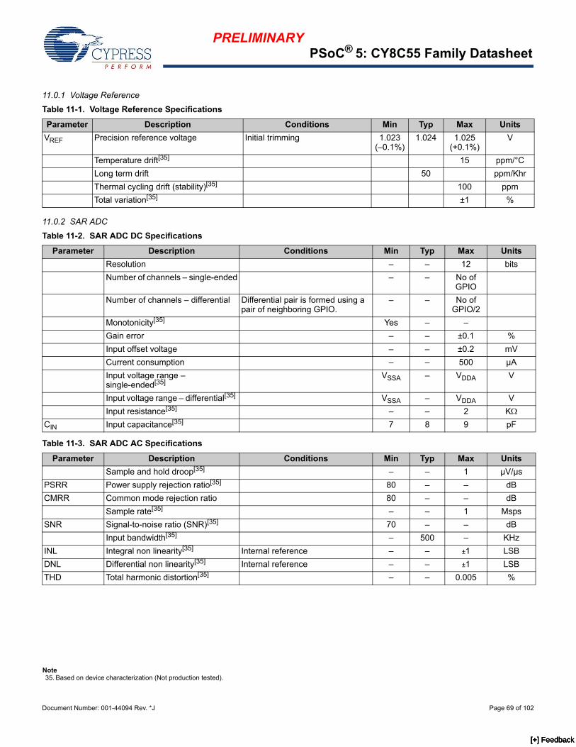
PRELIMINARYPSoC® 5: CY8C55 Family Datasheet
Document Number: 001-44094 Rev. *J Page 69 of 102
11.0.1 Voltage Reference
11.0.2 SAR ADC
Note35. Based on device characterization (Not production tested).
Table 11-1. Voltage Reference Specifications
Parameter Description Conditions Min Typ Max Units
VREF Precision reference voltage Initial trimming 1.023 (–0.1%)
1.024 1.025 (+0.1%)
V
Temperature drift[35] 15 ppm/°C
Long term drift 50 ppm/Khr
Thermal cycling drift (stability)[35] 100 ppm
Total variation[35] ±1 %
Table 11-2. SAR ADC DC Specifications
Parameter Description Conditions Min Typ Max Units
Resolution – – 12 bits
Number of channels – single-ended – – No of GPIO
Number of channels – differential Differential pair is formed using a pair of neighboring GPIO.
– – No of GPIO/2
Monotonicity[35] Yes – –
Gain error – – ±0.1 %
Input offset voltage – – ±0.2 mV
Current consumption – – 500 µA
Input voltage range – single-ended[35]
VSSA – VDDA V
Input voltage range – differential[35] VSSA – VDDA V
Input resistance[35] – – 2 K
CIN Input capacitance[35] 7 8 9 pF
Table 11-3. SAR ADC AC Specifications
Parameter Description Conditions Min Typ Max Units
Sample and hold droop[35] – – 1 µV/µs
PSRR Power supply rejection ratio[35] 80 – – dB
CMRR Common mode rejection ratio 80 – – dB
Sample rate[35] – – 1 Msps
SNR Signal-to-noise ratio (SNR)[35] 70 – – dB
Input bandwidth[35] – 500 – KHz
INL Integral non linearity[35] Internal reference – – ±1 LSB
DNL Differential non linearity[35] Internal reference – – ±1 LSB
THD Total harmonic distortion[35] – – 0.005 %
[+] Feedback [+] Feedback [+] Feedback [+] Feedback

PRELIMINARYPSoC® 5: CY8C55 Family Datasheet
Document Number: 001-44094 Rev. *J Page 70 of 102
11.0.3 Analog Globals
11.0.4 Comparator
Table 11-4. Analog Globals AC Specifications
Parameter Description Conditions Min Typ Max Units
Rppag Resistance pin-to-pin through analog global[36]
VDDA = 3.0 V – 939 1461
Rppmuxbus Resistance pin-to-pin through analog mux bus[36]
VDDA = 3.0 V – 721 1135
BWag 3 dB bandwidth of analog globals VDDA = 3.0 V – – 2 MHz
CMRRag Common mode rejection for differential signals
VDDA = 3.0 V 85 91 – dB
Notes36. The resistance of the analog global and analog mux bus is high if VDDA 2.7 V, and the chip is in either sleep or hibernate mode. Use of analog global and analog
mux bus under these conditions is not recommended.37. The recommended procedure for using a custom trim value for the on-chip comparators can be found in the TRM.38. Based on device characterization (Not production tested).
Table 11-5. Comparator DC Specifications
Parameter Description Conditions Min Typ Max Units
VIOFFInput offset voltage in fast mode Factory trim – – ±2 mV
Input offset voltage in slow mode Factory trim – – ±2 mV
VIOFFInput offset voltage in fast mode[37] Custom trim – – ±2 mV
Input offset voltage in slow mode[37] Custom trim – – ±1 mV
VIOFF Input offset voltage in ultra low power mode
– ±12 – mV
VHYST Hysteresis Hysteresis enable mode – 10 32 mV
VICM Input common mode voltage Fast mode 0 – VDDA–0.1 V
Slow mode 0 – VDDA V
CMRR Common mode rejection ratio 50 – – dB
ICMP High current mode/fast mode[38] – – 400 µA
Low current mode/slow mode[38] – – 100 µA
Ultra low power mode[38] – 6 – µA
Table 11-6. Comparator AC Specifications
Parameter Description Conditions Min Typ Max Units
TRESP
Response time, high current mode[38]
50 mV overdrive, measured pin-to-pin
– 95 TBD ns
Response time, low current mode[38]
50 mV overdrive, measured pin-to-pin
– 155 TBD ns
Response time, ultra low power mode[38]
50 mV overdrive, measured pin-to-pin
– 55 – µs
[+] Feedback [+] Feedback [+] Feedback [+] Feedback

PRELIMINARYPSoC® 5: CY8C55 Family Datasheet
Document Number: 001-44094 Rev. *J Page 71 of 102
11.0.5 IDAC
11.0.6 VDAC
Note39. Based on device characterization (Not production tested).
Table 11-7. IDAC (Current Digital-to-Analog Converter) DC Specifications
Parameter Description Conditions Min Typ Max Units
Resolution – 8 –
IOUT Output current
High[39] Code = 255, VDDA 2.7 V, RL 600
– 2.040 – mA
Code = 255, VDDA 2.7 V, RL 300
– 2.040 – mA
Medium[39] Code = 255, RL 600 – 255 – µA
Low[39] Code = 255, RL 600 – 31.875 – µA
INL Integral non linearity RL 600 , CL=15 pF – – ±1 LSB
DNL Differential non linearity RL 600 , CL=15 pF – – ±0.5 LSB
Ezs Zero scale error – 0 ±1 LSB
Eg Gain error Uncompensated – – 3.5 %
Temperature compensated – – TBD %
IDAC_ICC DAC current low speed mode[39] Code = 0 – – 100 µA
IDAC_ICC DAC current high speed mode[39] Code = 0 – – 500 µA
Table 11-8. IDAC (Current Digital-to-Analog Converter) AC Specifications
Parameter Description Conditions Min Typ Max Units
FDAC Update rate – – 8 Msps
TSETTLE
Settling time to 0.5LSB Full scale transition, 600 load, CL = 15 pF
Fast mode Independent of IDAC range setting (IOUT)
– – 100 ns
Slow mode Independent of IDAC range setting (IOUT)
– – 1000 ns
Table 11-9. VDAC (Voltage Digital-to-Analog Converter) DC Specifications
Parameter Description Conditions Min Typ Max Units
Resolution – 8 –
ROUT
Output resistance[39]
High VOUT = 4 V – 16 – k Low VOUT = 1 V – 4 – k
VOUT
Output voltage range[39]
High Code = 255, VDDA > 5 V – 4 – V
Low Code = 255 – 1 – V
INL Integral non linearity CL=15 pF – – ±1 LSB
DNL Differential non linearity CL=15 pF – – ±1 LSB
Ezs Zero scale error – – ±1 LSB
Eg Gain error Uncompensated – – 3 %
Temperature compensated – – TBD %
VDAC_ICC DAC current low speed mode[39] Code = 0 – – 100 µA
VDAC_ICC DAC current high speed mode[39] Code = 0 – – 500 µA
[+] Feedback [+] Feedback [+] Feedback [+] Feedback
PRELIMINARYPSoC® 5: CY8C55 Family Datasheet
Document Number: 001-44094 Rev. *J Page 72 of 102
11.0.7 Discrete Time Mixer
The discrete time mixer is used for modulating (shifting signals in frequency down) where the output frequency of the mixer is equal to the difference of the input frequency and the local oscillator frequency. The discrete time mixer is created using a SC/CT analog block; see the Mixer component datasheet in PSoC Creator for full AC/DC specifications, and APIs and example code.
11.0.8 Continuous Time Mixer
The continuous time mixer is used for modulating (shift) frequencies up or down, to a limit of 1.0 MHz. The continuous time mixer is created using a SC/CT analog block; see the Mixer component datasheet in PSoC Creator for full AC/DC specifications, and APIs and example code.
Table 11-10. VDAC (Voltage Digital-to-Analog Converter) AC Specifications
Parameter Description Conditions Min Typ Max Units
FDACUpdate rate[40] 1 V mode – – 1 Msps
Update rate[40] 4 V mode – – 250 Ksps
TSETTLE
Settling time to 0.5LSB[40] Full scale transition, CL = 15 pF
High[40] VOUT = 4 V – – 4000 ns
Low[40] VOUT = 1 V – – 1000 ns
Table 11-11. Discrete Time Mixer DC Specifications
Parameter Description Conditions Min Typ. Max Units
Analog input noise injection (RMS) 1 MHz clock rate – 10 – µV
4 MHz clock rate – 30 – µV
Input voltage[41] VSSA – VDDA V
Input offset voltage – – 10 mV
Quiescent current – 0.9 2 mA
Table 11-12. Discrete Time Mixer AC Specifications
Parameter Description Conditions Min Typ Max Units
LO Local oscillator frequency[40] 0 – 4 MHz
Input signal frequency for down mixing[40]
0 – 14 MHz
Notes40. Based on device characterization (Not production tested).41. Bandwidth is guaranteed for input common mode between 0.3 V and VDDA-1.2 V and for output that is between 0.05 V and VDDA-0.05 V.
Table 11-13. Continuous Time Mixer DC Specifications
Parameter Description Conditions Min Typ Max Units
Analog input noise injection (RMS) No input signal – – 10 µV
Input voltage[41] VSSA – VDDA V
Input offset voltage – – 10 mV
Quiescent current – 0.9 2 mA
Table 11-14. Continuous Time Mixer AC Specifications
Parameter Description Conditions Min Typ Max Units
LO Local oscillator frequency[40] – – 1 MHz
Input signal frequency[40] – – 1 MHz
[+] Feedback [+] Feedback [+] Feedback [+] Feedback

PRELIMINARYPSoC® 5: CY8C55 Family Datasheet
Document Number: 001-44094 Rev. *J Page 73 of 102
11.0.9 Transimpedance Amplifier
The TIA is created using a SC/CT analog block; see the TIA component datasheet in PSoC Creator for full AC/DC specifications, and APIs and example code.
Table 11-15. Transimpedance Amplifier (TIA) DC Specifications
Parameter Description Conditions Min Typ Max Units
VIOFF Input offset voltage – – 10 mV
Rconv
Conversion resistance[42]
R = 20K 40 pF load –20 – +30 %
R = 30K 40 pF load –20 – +30 %
R = 40K 40 pF load –20 – +30 %
R = 80K 40 pF load –20 – +30 %
R = 120K 40 pF load –20 – +30 %
R = 250K 40 pF load –20 – +30 %
R= 500K 40 pF load –20 – +30 %
R = 1M 40 pF load –20 – +30 %
Quiescent current – 900 – µA
Table 11-16. Transimpedance Amplifier (TIA) AC Specifications
Parameter Description Conditions Min Typ Max Units
Input bandwidth (–3 dB) –20 pF load[43]
R = 20K 1800 – – kHz
R = 120K 330 – – kHz
R = 1M 47 – – kHz
Input bandwidth (3 dB) –40 pF load
R = 20K 1500 – – kHz
R = 120K 300 – – kHz
R = 1M 46 – – kHz
Notes42. Conversion resistance values are not calibrated. Calibrated values and details about calibration are provided in PSoC Creator component datasheets. External precision
resistors can also be used.43. Bandwidth is guaranteed for input common mode between 0.3 V and VDDA-1.2 V and for output that is between 0.05 V and VDDA-0.05 V.
[+] Feedback [+] Feedback [+] Feedback [+] Feedback

PRELIMINARYPSoC® 5: CY8C55 Family Datasheet
Document Number: 001-44094 Rev. *J Page 74 of 102
11.0.10 Programmable Gain Amplifier
The PGA is created using a SC/CT analog block; see the PGA component datasheet in PSoC Creator for full AC/DC specifications, and APIs and example code.
Table 11-17. PGA DC Specifications
Parameter Description Conditions Min Typ Max Units
VOS Input offset voltage[44] – – 10 mV
DeltaV/DeltaTa Input offset voltage drift[44] – ±30 µV/°C
Output current source capability[44]
Drive setting 3, VDDA = 1.71 V – – 250 µA
PSRR Power supply rejection ratio[44] 100 kHz 69 – – dB
1 MHz 38 – – dB
Zin Input impedance[44] For non inverting inputs 35 – – M
Gain Error[44] Non inverting mode, reference = VSSA
Ge1 Gain = 1 Rin of 40K – – ±0.15 %
Ge2 Gain = 2 Rin of 40K ±1 %
Ge4 Gain = 4 Rin of 40K – – ±1.03 %
Ge8 Gain = 8 Rin of 40K – – ±1.23 %
Ge16 Gain = 16 Rin of 40K – – ±2.5 %
Ge32 Gain = 32 Rin of 40K – – ±5 %
Ge50 Gain = 50 Rin of 40K – – ±5 %
VONL DC output non linearity G = 1[44] – – 0.01 % of FSR
VOH, VOL Output voltage swing VSSA + 0.15 – VDDA – 0.15 V
Quiescent current[44] – – 1.65 mA
Table 11-18. PGA AC Specifications
Parameter Description Conditions Min Typ Max Units
–3 db Bandwidth[44]
BW1 Gain = 1 Noninverting mode, 300 mV VIN VDDA –1.2 V, Cl 25 pF
7 – – MHz
BW24 Gain = 24 Noninverting mode, 300 mV VIN VDDA –1.2 V, Cl 25 pF
360 – – kHz
BW48 Gain = 48 Noninverting mode, 300 mV VIN VDDA –1.2 V, Cl 25 pF
215 – – kHz
Slew Rate[18]
SR1 Gain = 1 VDDA = 1.71 V 5% to 90% FS output
3 – – V/µs
SR24 Gain = 24 RC limited 0.5 – – V/µs
SR48 Gain = 48 RC limited 0.5 – – V/µs
Input Noise Voltage Density[44]
eni1 Gain = 1 10 kHz – 38 – nV/sqrtHz
eni24 Gain = 24 10 kHz – 38 – nV/sqrtHz
eni48 Gain = 48 10 kHz – 38 – nV/sqrtHz
Note44. Based on device characterization (Not production tested).
[+] Feedback [+] Feedback [+] Feedback [+] Feedback

PRELIMINARYPSoC® 5: CY8C55 Family Datasheet
Document Number: 001-44094 Rev. *J Page 75 of 102
11.0.11 Unity Gain Buffer
The unity gain buffer is created using a SC/CT analog block. See the Unity Gain Buffer component datasheet in PSoC Creator for full AC/DC specifications, and APIs and example code.
11.0.12 Temperature Sensor
Table 11-19. Unity Gain Buffer DC Specifications
Parameter Description Conditions Min Typ Max Units
VOS Input offset voltage[45] – – 10 mV
Offset voltage drift – – 30 µv/°C
Input voltage range VSSA – VDDA V
VOH, VOL Output voltage range VSSA + 0.15
– VDDA –0.15
V
Output current source capability[45] Drive setting 3, VDDA = 1.71 V – – 250 µA
Quiescent current – 900 – µA
Table 11-20. Unity Gain Buffer AC Specifications
Parameter Description Conditions Min Typ Max Units
Bandwidth[45, 46] Noninverting mode, 300 mV VIN VDDA –1.2 V, Cl 25 pF
7 – – MHz
Slew rate[45] VDDA = 1.71 V 5% to 90% FS output, CL = 50 pF
3 – – V/µs
Input noise spectral density[45] – 38 – nV/sqrtHz
Notes45. Based on device characterization (Not production tested).46. Bandwidth is guaranteed for input common mode between 0.3 V and VDDA-1.2 V and for output that is between 0.05 V and VDDA-0.05 V.
Table 11-21. Temperature Sensor Specifications
Parameter Description Conditions Min Typ Max Units
Temp sensor accuracy Range: –40 °C to +85 °C – ±5 – °C
[+] Feedback [+] Feedback [+] Feedback [+] Feedback

PRELIMINARYPSoC® 5: CY8C55 Family Datasheet
Document Number: 001-44094 Rev. *J Page 76 of 102
11.0.13 LCD Direct Drive
Table 11-22. LCD Direct Drive DC Specifications
Parameter Description Conditions Min Typ Max Units
ICC LCD operating current 16x4 segment display at 50 Hz [48]. – 19 – A
VBIAS LCD bias range (VBIAS refers to the main output voltage(V0) of LCD DAC)
VDDA 3 V and VDDA VBIAS 2 – 5.5 V
LCD bias step size VDDA 3 V and VDDA VBIAS – 9.1 x VDDA – mV
LCD capacitance per segment/common driver
Drivers may be combined. – 500 5000 pF
Long term segment offset – – 10 mV
IOUT (Output drive current per segment driver)
Strong drive Output current in strong drive mode for VDDIO = 5.5 V
528 – 655 µA
ICC per segment driver
Strong drive 220 260 300 µA
Weak drive – 11 – µA
Weak drive 2 – 22 – µA
No drive – <25 – nA
Static (1 common)
IccLCD LCD system operating current VBIAS = 5 VNumber of LCD pins: 33 (32x1)Number of segments: 32[47]
– 12 – µA
IccLCD LCD system operating current VBIAS = 3 VNumber of LCD pins: 33 (32x1)Number of segments: 32[47]
– 10 – µA
1/4 duty (4 commons)
IccLCD LCD system operating current VBIAS = 5 VNumber of LCD pins: 36 (32x4)Number of segments: 128[47]
– 24 – µA
IccLCD LCD system operating current VBIAS = 3 VNumber of LCD pins: 36 (32x4)Number of segments: 128[47]
– 21 – µA
1/16 duty (16 commons)
IccLCD LCD system operating current VBIAS = 5 VNumber of LCD pins: 48 (32x16)Number of segments: 512[47]
– 93 – µA
IccLCD LCD system operating current VBIAS = 3 VNumber of LCD pins: 48 (32x16)Number of segments: 512[47]
– 83 – µA
Notes47. Additional conditions: All segments on; 2000 pF glass capacitance; Type A waveform; 32 Hz LCD refresh rate; Operating temperature = 25 °C; Boost converter not
used.48. This is the LCD system operating current when there is no LCD display. Connecting an actual LCD display increases the current consumption based on the size of
the LCD glass.
Table 11-23. LCD Direct Drive AC Specifications
Parameter Description Conditions Min Typ Max Units
fLCD LCD frame rate 10 50 150 Hz
[+] Feedback [+] Feedback [+] Feedback [+] Feedback

PRELIMINARYPSoC® 5: CY8C55 Family Datasheet
Document Number: 001-44094 Rev. *J Page 77 of 102
11.1 Digital Peripherals
Specifications are valid for –40 °C TA 85 °C and TJ 100 °C, except where noted. Specifications are valid for 1.71 V to 5.5 V, except where noted.
11.1.1 Timer
11.1.2 Counter
Table 11-24. Timer DC Specifications
Parameter Description Conditions Min Typ Max Units
Block current consumption 16-bit timer, at listed input clock frequency
– – – µA
3 MHz – 8 – µA
12 MHz – 30 – µA
48 MHz – 120 – µA
67 MHz – 165 – µA
80 MHz – 195 – µA
Table 11-25. Timer AC Specifications
Parameter Description Conditions Min Typ Max Units
Operating frequency DC – 80 MHz
Capture pulse width (Internal) 13 – – ns
Capture pulse width (external) 30 – – ns
Timer resolution 13 – – ns
Enable pulse width 13 – – ns
Enable pulse width (external) 30 – – ns
Reset pulse width 13 – – ns
Reset pulse width (external) 30 – – ns
Table 11-26. Counter DC Specifications
Parameter Description Conditions Min Typ Max Units
Block current consumption 16-bit counter, at listed input clock frequency
– – – µA
3 MHz – 8 – µA
12 MHz – 30 – µA
48 MHz – 120 – µA
67 MHz – 165 – µA
80 MHz – 195 – µA
Table 11-27. Counter AC Specifications
Parameter Description Conditions Min Typ Max Units
Operating frequency DC – 80 MHz
Capture pulse 13 – – ns
Resolution 13 – – ns
Pulse width 13 – – ns
Pulse width (external) 30 ns
Enable pulse width 13 – – ns
Enable pulse width (external) 30 – – ns
Reset pulse width 13 – – ns
Reset pulse width (external) 30 – – ns
[+] Feedback [+] Feedback [+] Feedback [+] Feedback

PRELIMINARYPSoC® 5: CY8C55 Family Datasheet
Document Number: 001-44094 Rev. *J Page 78 of 102
11.1.3 Pulse Width Modulation
11.1.4 I2C
11.1.5 Controller Area Network[49]
Table 11-28. PWM DC Specifications
Parameter Description Conditions Min Typ Max Units
Block current consumption 16-bit PWM, at listed input clock frequency
– – – µA
3 MHz – 8 – µA
12 MHz – 30 – µA
48 MHz – 120 – µA
67 MHz – 165 – µA
80 MHz – 195 – µA
Table 11-29. PWM AC Specifications
Parameter Description Conditions Min Typ Max Units
Operating frequency DC – 80 MHz
Pulse width 13 – – ns
Pulse width (external) 30 – – ns
Kill pulse width 13 – – ns
Kill pulse width (external) 30 – – ns
Enable pulse width 13 – – ns
Enable pulse width (external) 30 – – ns
Reset pulse width 13 – – ns
Reset pulse width (external) 30 – – ns
Table 11-30. Fixed I2C DC Specifications
Parameter Description Conditions Min Typ Max Units
Block current consumption Enabled, configured for 100 kbps – – 64 µA
Enabled, configured for 400 kbps – – 74 µA
Wake from sleep mode – – TBD µA
Table 11-31. Fixed I2C AC Specifications
Parameter Description Conditions Min Typ Max Units
Bit rate – – 1 Mbps
Note49. Refer to ISO 11898 specification for details.
Table 11-32. CAN DC Specifications
Parameter Description Conditions Min Typ Max Units
Block current consumption 500 kbps – – 285 µA
1 Mbps – – 330 µA
Table 11-33. CAN AC Specifications
Parameter Description Conditions Min Typ Max Units
Bit rate Minimum 8 MHz clock – – 1 Mbit
[+] Feedback [+] Feedback [+] Feedback [+] Feedback

PRELIMINARYPSoC® 5: CY8C55 Family Datasheet
Document Number: 001-44094 Rev. *J Page 79 of 102
11.1.6 Digital Filter Block
11.1.7 USB
Table 11-34. DFB DC Specifications
Parameter Description Conditions Min Typ Max Units
DFB operating current 64-tap FIR at FDFB
100 kHz (1.3 ksps) – 0.03 0.05 mA
500 kHz (6.7 ksps) – 0.16 0.27 mA
1 MHz (13.4 ksps) – 0.33 0.53 mA
10 MHz (134 ksps) – 3.3 5.3 mA
48 MHz (644 ksps) – 15.7 25.5 mA
67 MHz (900 ksps) – 21.8 35.6 mA
80 MHz (1.07 Msps) – 26.1 42.5 mA
Table 11-35. DFB AC Specifications
Parameter Description Conditions Min Typ Max Units
FDFB DFB operating frequency DC – 80 MHz
Table 11-36. USB DC Specifications
Parameter Description Conditions Min Typ Max Units
Operating current USB enabled bus idle – 0.68 – mA
[+] Feedback [+] Feedback [+] Feedback [+] Feedback

PRELIMINARYPSoC® 5: CY8C55 Family Datasheet
Document Number: 001-44094 Rev. *J Page 80 of 102
11.1.8 Universal Digital Blocks (UDBs)
PSoC Creator provides a library of pre-built and tested standard digital peripherals (UART, SPI, LIN, PRS, CRC, timer, counter, PWM, AND, OR, and so on) that are mapped to the UDB array. See the component datasheets in PSoC Creator for full AC/DC specifications, APIs, and example code.
Figure 11-9. Clock to Output Performance
Table 11-37. UDB AC Specifications
Parameter Description Conditions Min Typ Max Units
Datapath Performance
FMAX_TIMER Maximum frequency of 16-bit timer in a UDB pair
– – 80 MHz
FMAX_ADDER Maximum frequency of 16-bit adder in a UDB pair
– – 80 MHz
FMAX_CRC Maximum frequency of 16-bit CRC/PRS in a UDB pair
– – 80 MHz
PLD Performance
FMAX_PLD Maximum frequency of a two-pass PLD function in a UDB pair
– – 80 MHz
Clock to Output Performance
tCLK_OUT Propagation delay for clock in to data out, see Figure 11-9.
25 °C operating temperature – TBD TBD ns
tCLK_OUT Propagation delay for clock in to data out, see Figure 11-9.
Worst-case placement, routing, and pin selection
– TBD TBD ns
[+] Feedback [+] Feedback [+] Feedback [+] Feedback

PRELIMINARYPSoC® 5: CY8C55 Family Datasheet
Document Number: 001-44094 Rev. *J Page 81 of 102
11.1 Memory
Specifications are valid for –40 °C TA 85 °C and TJ 100 °C, except where noted. Specifications are valid for 1.71 V to 5.5 V, except where noted.
11.1.1 Flash
11.1.2 EEPROM
11.1.3 Nonvolatile Latches (NVL)
Table 11-1. Flash DC Specifications
Parameter Description Conditions Min Typ Max Units
Erase and program voltage VDDD pin 1.71 – 5.5 V
Table 11-2. Flash AC Specifications
Parameter Description Conditions Min Typ Max Units
TWRITE Row write time (erase + program) – – 15 ms
TERASE Row erase time – – 10 ms
Row program time – – 5 ms
TBULK Bulk erase time (256 KB) – – 80 ms
Sector erase time (16 KB) – – 15 ms
Total device program time (including JTAG, and so on)
– – 5 seconds
Flash endurance 100k – – program/erase cycles
Flash data retention time Retention period measured from last erase cycle
20 – – years
Table 11-3. EEPROM DC Specifications
Parameter Description Conditions Min Typ Max Units
Erase and program voltage 1.71 – 5.5 V
Table 11-4. EEPROM AC Specifications
Parameter Description Conditions Min Typ Max Units
TWRITE Single byte erase/write cycle time – 2 15 ms
EEPROM endurance 1M – – program/erase cycles
EEPROM data retention time Retention period measured from last erase cycle (up to 100 K cycles)
20 – – years
Table 11-5. NVL DC Specifications
Parameter Description Conditions Min Typ Max Units
Erase and program voltage VDDD pin 1.71 – 5.5 V
[+] Feedback [+] Feedback [+] Feedback [+] Feedback

PRELIMINARYPSoC® 5: CY8C55 Family Datasheet
Document Number: 001-44094 Rev. *J Page 82 of 102
11.1.4 SRAM
11.1.5 External Memory Interface
Figure 11-1. Asynchronous Read Cycle Timing
Table 11-6. NVL AC Specifications
Parameter Description Conditions Min Typ Max Units
NVL endurance Programmed at 25 °C 1K – – program/erase cycles
Programmed at 0 °C to 70 °C 100 – – program/erase cycles
NVL data retention time Programmed at 25 °C 20 – – years
Programmed at 0 °C to 70 °C 20 – – years
Table 11-7. SRAM DC Specifications
Parameter Description Conditions Min Typ Max Units
VSRAM SRAM retention voltage 1.2 – – V
Table 11-8. SRAM AC Specifications
Parameter Description Conditions Min Typ Max Units
FSRAM SRAM operating frequency DC – 80 MHz
Table 11-1. Asynchronous Read Cycle Specifications
Parameter Description Conditions Min Typ Max Units
T EMIF clock period 30.3 – – ns
Tcel EM_CEn low time 2 × T – 1 – 2 × T + 2 ns
Taddrv EM_CEn low to EM_Addr valid – – 5 ns
Taddrh Address hold time after EM_OEn high 2 – – ns
Toev EM_CEn low to EM_OEn low –5 – 5 ns
EM_Addr
EM_CEn
EM_OEn
EM_Data
EM_WEn
Address
Data
Tcel
Taddrv Taddrh
Toev ToelToeh
Tdcesu
Tdoesu
TdcehTdoeh
[+] Feedback [+] Feedback [+] Feedback [+] Feedback

PRELIMINARYPSoC® 5: CY8C55 Family Datasheet
Document Number: 001-44094 Rev. *J Page 83 of 102
Figure 11-2. Asynchronous Write Cycle Timing
Toel EM_OEn low time 2 × T – 1 – 2 × T + 2 ns
Toeh EM_OEn high to EM_CEn high hold time –5 – 5 ns
Tdoesu Data to EM_OEn high setup time T + 20 – – ns
Tdcesu Data to EM_CEn high setup time T + 20 – – ns
Tdoeh Data hold time after EM_OEn high 3 – – ns
Tdceh Data hold time after EM_CEn high 3 – – ns
Table 11-1. Asynchronous Write Cycle Specifications
Parameter Description Conditions Min Typ Max Units
T EMIF clock period 30.3 – – ns
Taddrv EM_CEn low to EM_Addr valid – – 5 ns
Taddrh Address hold time after EM_WEn high T+2 – – ns
Tcel EM_CEn low time 2 × T – 1 – 2 × T + 2 ns
Twev EM_CEn low to EM_WEn low –5 – 5 ns
Twel EM_WEn low time T – 1 – T + 2 ns
Tweh EM_WEn high to EM_CEn high hold time T – – ns
Tdcev EM_CEn low to data valid – – 7 ns
Tdweh Data hold time after EM_WEn high T – – ns
Table 11-1. Asynchronous Read Cycle Specifications (continued)
Parameter Description Conditions Min Typ Max Units
Address
Data
Taddrv Taddrh
Tcel
Twev Twel Tweh
TdcevTdweh
EM_Data
EM_OEn
EM_CEn
EM_Addr
EM_WEn
[+] Feedback [+] Feedback [+] Feedback [+] Feedback

PRELIMINARYPSoC® 5: CY8C55 Family Datasheet
Document Number: 001-44094 Rev. *J Page 84 of 102
Figure 11-3. Synchronous Read Cycle Timing
Table 11-1. Synchronous Read Cycle Specifications
Parameter Description Conditions Min Typ Max Units
T EMIF clock period 30.3 – – ns
Tcp EM_clock period 30.3 – – ns
Tceld EM_clock low to EM_CEn low – 5 ns
Tcehd EM_clock high to EM_CEn high T/2 – 2 – – ns
Taddrv EM_clock low to EM_Addr valid – – 5 ns
Taddriv EM_clock high to EM_Addr invalid T/2 – 2 – – ns
Toeld EM_clock low to EM_OEn low – – 5 ns
Toehd EM_clock high to EM_OEn high T + 2 – – ns
Tds Data valid before EM_Clock high 20 – – ns
Tdh Data valid after EM_Clock high 2 – – ns
Tadscld EM_clock low to EM_ADSCn low – – 5 ns
Tadschd EM_clock high to EM_ADSCn high T/2 – 2 – – ns
Address
Tcp
Tceld
Taddrv
Tcehd
Taddriv
ToehdToeld
Tds
TadscldTadschd
Data
Tdh
EM_ Clock
EM_CEn
EM_Addr
EM_OEn
EM_Data
EM_ ADSCn
[+] Feedback [+] Feedback [+] Feedback [+] Feedback

PRELIMINARYPSoC® 5: CY8C55 Family Datasheet
Document Number: 001-44094 Rev. *J Page 85 of 102
Figure 11-4. Synchronous Write Cycle Timing
Table 11-1. Synchronous Write Cycle Specifications
Parameter Description Conditions Min Typ Max Units
T EMIF clock period 30.3 – – ns
Tcp EM_clock Period 30.3 – – ns
Tceld EM_clock low to EM_CEn low – – 5 ns
Tcehd EM_clock high to EM_CEn high T/2 – 2 – – ns
Taddrv EM_clock low to EM_Addr valid – – 5 ns
Taddriv EM_clock high to EM_Addr invalid T/2 – 2 – – ns
Tweld EM_clock low to EM_WEn low – – 5 ns
Twehd EM_clock high to EM_WEn high T/2 – 2 – – ns
Tds Data valid after EM_Clock low – – 5 ns
Tadscld EM_clock low to EM_ADSCn low – – 5 ns
Tadschd EM_clock high to EM_ADSCn high T/2 – 2 – – ns
Address
Tcp
Tceld
Taddrv
Tcehd
Taddriv
TwehdTweld
Tds
Data
TadscldTadschd
EM_ Clock
EM_CEn
EM_Addr
EM_WEn
EM_Data
EM_ ADSCn
[+] Feedback [+] Feedback [+] Feedback [+] Feedback

PRELIMINARYPSoC® 5: CY8C55 Family Datasheet
Document Number: 001-44094 Rev. *J Page 86 of 102
11.1 PSoC System Resources
Specifications are valid for –40 °C TA 85 °C and TJ 100 °C, except where noted. Specifications are valid for 1.71 V to 5.5 V, except where noted.
11.1.1 POR with Brown Out
For brown out detect in regulated mode, VDDD and VDDA must be 2.0 V. Brown out detect is available in externally regulated mode.
11.1.2 Voltage Monitors
Table 11-2. Precise Power On Reset (PRES) with Brown Out DC Specifications
Parameter Description Conditions Min Typ Max Units
Precise POR (PPOR)
PRESR Rising trip voltage 1.66 – 1.73 V
PRESF Falling trip voltage 1.63 – 1.70 V
Table 11-3. Power On Reset (POR) with Brown Out AC Specifications
Parameter Description Conditions Min Typ Max Units
PRES_TR Response time – – 250 ns
VDDD/VDDA drop rate Sleep mode – 5 TBD V/µs
Table 11-4. Voltage Monitors DC Specifications
Parameter Description Conditions Min Typ Max Units
LVI Trip voltage
LVI_A/D_SEL[3:0] = 0000b 1.68 1.73 1.77 V
LVI_A/D_SEL[3:0] = 0001b 1.91 1.95 1.99 V
LVI_A/D_SEL[3:0] = 0010b 2.16 2.21 2.25 V
LVI_A/D_SEL[3:0] = 0011b 2.40 2.45 2.50 V
LVI_A/D_SEL[3:0] = 0100b 2.65 2.71 2.76 V
LVI_A/D_SEL[3:0] = 0101b 2.90 2.96 3.01 V
LVI_A/D_SEL[3:0] = 0110b 3.14 3.21 3.27 V
LVI_A/D_SEL[3:0] = 0111b 3.39 3.46 3.53 V
LVI_A/D_SEL[3:0] = 1000b 3.63 3.71 3.78 V
LVI_A/D_SEL[3:0] = 1001b 3.88 3.96 4.03 V
LVI_A/D_SEL[3:0] = 1010b 4.12 4.21 4.29 V
LVI_A/D_SEL[3:0] = 1011b 4.36 4.45 4.54 V
LVI_A/D_SEL[3:0] = 1100b 4.61 4.70 4.79 V
LVI_A/D_SEL[3:0] = 1101b 4.88 4.98 5.08 V
LVI_A/D_SEL[3:0] = 1110b 5.11 5.22 5.32 V
LVI_A/D_SEL[3:0] = 1111b 5.36 5.47 5.57 V
HVI Trip voltage 5.630 5.745 5.860 V
Table 11-5. Voltage Monitors AC Specifications
Parameter Description Conditions Min Typ Max Units
Response time – – 500 ns
[+] Feedback [+] Feedback [+] Feedback [+] Feedback

PRELIMINARYPSoC® 5: CY8C55 Family Datasheet
Document Number: 001-44094 Rev. *J Page 87 of 102
11.1.3 Interrupt Controller
11.1.4 JTAG Interface
11.1.5 SWD Interface
11.1.6 TPIU Interface
Table 11-6. Interrupt Controller AC Specifications
Parameter Description Conditions Min Typ Max Units
Delay from interrupt signal input to ISR code execution from main line code
Includes worse case completion of longest instruction DIV with 6 cycles
– – 20 Tcy CPU
Delay from interrupt signal input to ISR code execution from ISR code
Includes worse case completion of longest instruction DIV with 6 cycles
– – 20 Tcy CPU
Table 11-7. JTAG Interface AC Specifications[50]
Parameter Description Conditions Min Typ Max Units
f_TCK TCK frequency 3.3 V VDDD 5 V – – 14[51] MHz
1.71 V VDDD < 3.3 V – – 7[51] MHz
T_TDI_setup TDI, TMS setup before TCK high 0 – – ns
T_TDI_hold TDI, TMS hold after TCK high T = 1/f_TCK T/4 – –
T_TDO_valid TCK low to TDO valid T = 1/f_TCK 2T/5 – –
T_TDO_hold TDO hold after TCK high T = 1/f_TCK T/4 – –
TCK to device outputs valid – – TBD ns
Table 11-8. SWD Interface AC Specifications[50]
Parameter Description Conditions Min Typ Max Units
f_SWDCK SWDCLK frequency 3.3 V VDDD 5 V – – 14[52] MHz
1.71 V VDDD < 3.3 V – – 7[52] MHz
1.71 V VDDD < 3.3 V, SWD over USBIO pins
– – 5.5[52] MHz
T_SWDI_setup SWDIO input setup before SWDCK high T = 1/f_SWDCK T/4 – –
T_SWDI_hold SWDIO input hold after SWDCK high T = 1/f_SWDCK T/4 – –
T_SWDO_valid SWDCK low to SWDIO output valid T = 1/f_SWDCK 2T/5 – –
T_SWDO_hold SWDIO output hold after SWDCK high T = 1/f_SWDCK T/4 – –
Notes50. Based on device characterization (Not production tested).51. f_TCK must also be no more than 1/3 CPU clock frequency.52. f_SWDCK must also be no more than 1/3 CPU clock frequency. 53. TRACEPORT signal frequency and bit rate are limited by GPIO output frequency, see AC Specifications in “GPIO” on page 58.
Table 11-9. TPIU Interface AC Specifications[50]
Parameter Description Conditions Min Typ Max Units
TRACEPORT (TRACECLK) frequency – – 33[53] MHz
SWV bit rate – – 33[53] Mbit
[+] Feedback [+] Feedback [+] Feedback [+] Feedback

PRELIMINARYPSoC® 5: CY8C55 Family Datasheet
Document Number: 001-44094 Rev. *J Page 88 of 102
11.2 Clocking
Specifications are valid for –40 °C TA 85 °C and TJ 100 °C, except where noted. Specifications are valid for 1.71 V to 5.5 V, except where noted.
11.2.1 32 kHz External Crystal
11.2.2 Internal Main Oscillator)
Note54. Based on device characterization (Not production tested).
Table 11-10. 32 kHz External Crystal DC Specifications[54]
Parameter Description Conditions Min Typ Max Units
ICC Operating current Low power mode – – 0.25 µA
CL External crystal capacitance – 6 – pF
DL Drive level – – 1 µW
Table 11-11. 32 kHz External Crystal AC Specifications
Parameter Description Conditions Min Typ Max Units
F Frequency – 32.768 – kHz
DC Output duty cycle[54] 20 50 80 %
TON Startup time High power mode – 1 – s
Table 11-12. IMO DC Specifications
Parameter Description Conditions Min Typ Max Units
Supply current
74.7 MHz – – 600 µA
48 MHz – – 500 µA
24 MHz – USB mode With oscillator locking to USB bus – – 500 µA
24 MHz – non-USB mode – – 300 µA
12 MHz – – 200 µA
6 MHz – – 180 µA
3 MHz – – 150 µA
Table 11-13. IMO AC Specifications
Parameter Description Conditions Min Typ Max Units
FIMO
IMO frequency stability (with factory trim)
74.7 MHz –7 – 7 %
48 MHz –5 – 5 %
24 MHz – non-USB mode –4 – 4 %
24 MHz – USB mode With oscillator locking to USB bus –0.25 – 0.25 %
12 MHz –3 – 3 %
6 MHz –2 – 2 %
3 MHz –1 – 1 %
Startup time[54] From enable (during normal system operation) or wakeup from low power state
– – 12 µs
[+] Feedback [+] Feedback [+] Feedback [+] Feedback

PRELIMINARYPSoC® 5: CY8C55 Family Datasheet
Document Number: 001-44094 Rev. *J Page 89 of 102
11.2.3 Internal Low Speed Oscillator
11.2.4 External Crystal Oscillator
Jp-p
Jitter (peak to peak)[55]
F = 24 MHz – 0.9 – ns
F = 3 MHz – 1.6 – ns
Jperiod
Jitter (long term)[18]
F = 24 MHz – 0.9 – ns
F = 3 MHz – 12 – ns
Table 11-13. IMO AC Specifications (continued)
Parameter Description Conditions Min Typ Max Units
Note55. Based on device characterization (Not production tested).
Table 11-14. ILO DC Specifications
Parameter Description Conditions Min Typ Max Units
ICC
Operating current FOUT = 1 kHz – 0.3 1.7 µA
FOUT = 33 kHz – 1.0 2.6 µA
FOUT = 100 kHz – 1.0 2.6 µA
Leakage current Power down mode – 2.0 15 nA
Table 11-15. ILO AC Specifications
Parameter Description Conditions Min Typ Max Units
Startup time Turbo mode – – 2 ms
Startup time Non turbo mode, pd_mode = 0 – – 2 ms
Startup time Non turbo mode, pd_mode = 1 – – 15 ms
Duty cycle 47 50 53 %
FILO
ILO frequencies (trimmed)
100 kHz 45 100 200 kHz
1 kHz 0.5 1 2 kHz
ILO frequencies (untrimmed)
100 kHz 30 100 300 kHz
1 kHz 0.3 1 3.5 kHz
Table 11-16. ECO AC Specifications
Parameter Description Conditions Min Typ Max Units
F Crystal frequency range 4 – 33 MHz
DC Duty cycle[55] 40 50 60 %
[+] Feedback [+] Feedback [+] Feedback [+] Feedback

PRELIMINARYPSoC® 5: CY8C55 Family Datasheet
Document Number: 001-44094 Rev. *J Page 90 of 102
11.2.5 External Clock Reference
11.2.6 Phase-Locked Loop
Table 11-17. External Clock Reference AC Specifications[56]
Parameter Description Conditions Min Typ Max Units
External frequency range 0 – 33 MHz
Input duty cycle range Measured at VDDIO/2 30 50 70 %
Input edge rate VIL to VIH 0.1 – – V/ns
Table 11-18. PLL DC Specifications
Parameter Description Conditions Min Typ Max Units
IDD PLL operating current In = 3 MHz, Out = 80 MHz – 400 – µA
In = 3 MHz, Out = 24 MHz – 200 – µA
Table 11-19. PLL AC Specifications
Parameter Description Conditions Min Typ Max Units
Fpllin PLL input frequency[57] 1 – 48 MHz
PLL intermediate frequency[58] Output of prescaler 1 – 3 MHz
Fpllout PLL output frequency[57] 24 – 67 MHz
Lock time at startup – – 250 µs
Jperiod-rms Jitter (rms)[56] – – 250 ps
PLL output duty cycle All PLL output frequencies 45 – 55 %
Notes56. Based on device characterization (Not production tested).57. This specification is guaranteed by testing the PLL across the specified range using the IMO as the source for the PLL.58. PLL input divider, Q, must be set so that the input frequency is divided down to the intermediate frequency range. Value for Q ranges from 1 to 16.
[+] Feedback [+] Feedback [+] Feedback [+] Feedback

PRELIMINARYPSoC® 5: CY8C55 Family Datasheet
Document Number: 001-44094 Rev. *J Page 91 of 102
12. Ordering Information
In addition to the features listed in Table 12-1, every CY8C55 device includes: up to 256 KB flash, 64 KB SRAM, 2 KB EEPROM, a precision on-chip voltage reference, precision oscillators, flash, ECC, DMA, a fixed function I2C, JTAG/SWD programming and debug, external memory interface, and more. In addition to these features, the flexible UDBs and analog subsection support a wide range of peripherals. To assist you in selecting the ideal part, PSoC Creator makes a part recommendation after you choose the components required by your application. All CY8C55 derivatives incorporate device and flash security in user-selectable security levels; see the TRM for details.
Notes59. Analog blocks support a wide variety of functionality including TIA, PGA, and mixers. See Example Peripherals on page 31 for more information on how analog blocks
can be used.60. UDBs support a wide variety of functionality including SPI, LIN, UART, timer, counter, PWM, PRS, and others. Individual functions may use a fraction of a UDB or
multiple UDBs. Multiple functions can share a single UDB. See Example Peripherals on page 31 for more information on how UDBs can be used.61. The I/O Count includes all types of digital I/O: GPIO, SIO, and the two USB I/O. See I/O System and Routing on page 25 for details on the functionality of each of
these types of I/O.62. The JTAG ID has three major fields. The most significant nibble (left digit) is the version, followed by a 2 byte part number and a 3 nibble manufacturer ID.
Table 12-1. CY8C55 Family with ARM Cortex-M3 CPU
Part Number
MCU Core Analog Digital I/O[61]
Package JTAG ID[62]
CP
U S
pee
d (
MH
z)
Fla
sh (
KB
)
SR
AM
(K
B)
EE
PR
OM
(K
B)
LC
D S
egm
ent
Dri
ve
AD
Cs
DA
C
Co
mp
ara
tors
SC
/CT
An
alo
g B
lock
s[59
]
Op
amp
s
DF
B
Cap
Sen
se
UD
Bs[6
0]
16-b
it T
imer
/PW
M
FS
US
B
CA
N 2
.0b
Tota
l I/O
GP
IO
SIO
US
BIO
32 KB Flash
CY8C5585AXI-004 80 32 8 2 ✔ 1x20-bit Del-Sig1x12-bit SAR
4 4 4 4 ✔ ✔ 20 4 ✔ – 72 62 8 2 100-pin TQFP 0x0E104069
CY8C5585LTI-111 80 32 8 2 ✔ 1x20-bit Del-Sig1x12-bit SAR
4 4 4 4 ✔ ✔ 20 4 ✔ – 48 38 8 2 68-pin QFN 0x0E16F069
CY8C5585PVI-048 80 32 8 2 ✔ 1x20-bit Del-Sig1x12-bit SAR
4 4 4 4 ✔ ✔ 20 4 ✔ – 31 25 4 2 48-SSOP 0x0E130069
CY8C5585AXI-049 80 32 8 2 ✔ 1x20-bit Del-Sig1x12-bit SAR
4 4 4 4 ✔ ✔ 20 4 ✔ ✔ 72 62 8 2 100-pin TQFP 0x0E131069
CY8C5585PVI-090 80 32 8 2 ✔ 1x20-bit Del-Sig1x12-bit SAR
4 4 4 4 ✔ ✔ 20 4 ✔ ✔ 31 25 4 2 48-SSOP 0x0E15A069
64 KB Flash
CY8C5586AXI-061 80 64 16 2 ✔ 1x20-bit Del-Sig1x12-bit SAR
4 4 4 4 ✔ ✔ 24 4 ✔ – 72 62 8 2 100-pin TQFP 0x0E13D069
CY8C5586LTI-017 80 64 16 2 ✔ 1x20-bit Del-Sig1x12-bit SAR
4 4 4 4 ✔ ✔ 24 4 ✔ – 48 38 8 2 68-pin QFN 0x0E111069
CY8C5586PVI-084 80 64 16 2 ✔ 1x20-bit Del-Sig1x12-bit SAR
4 4 4 4 ✔ ✔ 24 4 ✔ – 31 25 4 2 48-SSOP 0x0E154069
CY8C5586AXI-058 80 64 16 2 ✔ 1x20-bit Del-Sig1x12-bit SAR
4 4 4 4 ✔ ✔ 24 4 ✔ ✔ 72 62 8 2 100-pin TQFP 0x0E13A069
CY8C5586PVI-107 80 64 16 2 ✔ 1x20-bit Del-Sig1x12-bit SAR
4 4 4 4 ✔ ✔ 24 4 ✔ ✔ 31 25 4 2 48-SSOP 0x0E16B069
128 KB Flash
CY8C5587AXI-019 80 128 32 2 ✔ 1x20-bit Del-Sig1x12-bit SAR
4 4 4 4 ✔ ✔ 24 4 ✔ – 72 62 8 2 100-pin TQFP 0x0E113069
CY8C5587LTI-079 80 128 32 2 ✔ 1x20-bit Del-Sig1x12-bit SAR
4 4 4 4 ✔ ✔ 24 4 ✔ – 48 38 8 2 68-pin QFN 0x0E14F069
CY8C5587PVI-073 80 128 32 2 ✔ 1x20-bit Del-Sig1x12-bit SAR
4 4 4 4 ✔ ✔ 24 4 ✔ - 31 25 4 2 48-SSOP 0x0E149069
CY8C5587AXI-102 80 128 32 2 ✔ 1x20-bit Del-Sig1x12-bit SAR
4 4 4 4 ✔ ✔ 24 4 ✔ ✔ 72 62 8 2 100-pin TQFP 0x0E166069
CY8C5587PVI-095 80 128 32 2 ✔ 1x20-bit Del-Sig1x12-bit SAR
4 4 4 4 ✔ ✔ 24 4 ✔ ✔ 31 25 4 2 48-SSOP 0x0E15F069
256 KB Flash
[+] Feedback [+] Feedback [+] Feedback [+] Feedback

PRELIMINARYPSoC® 5: CY8C55 Family Datasheet
Document Number: 001-44094 Rev. *J Page 92 of 102
CY8C5588AXI-022 80 256 64 2 ✔ 1x20-bit Del-Sig1x12-bit SAR
4 4 4 4 ✔ ✔ 24 4 ✔ – 72 62 8 2 100-pin TQFP 0x0E116069
CY8C5588LTI-052 80 256 64 2 ✔ 1x20-bit Del-Sig1x12-bit SAR
4 4 4 4 ✔ ✔ 24 4 ✔ - 48 38 8 2 68-pin QFN 0x0E134069
CY8C5588PVI-065 80 256 64 2 ✔ 1x20-bit Del-Sig1x12-bit SAR
4 4 4 4 ✔ ✔ 24 4 ✔ - 31 25 4 2 48-SSOP 0x0E141069
CY8C5588AXI-020 80 256 64 2 ✔ 1x20-bit Del-Sig1x12-bit SAR
4 4 4 4 ✔ ✔ 24 4 ✔ ✔ 72 62 8 2 100-pin TQFP 0x0E114069
CY8C5588PVI-067 80 256 64 2 ✔ 1x20-bit Del-Sig1x12-bit SAR
4 4 4 4 ✔ ✔ 24 4 ✔ ✔ 31 25 4 2 48-SSOP 0x0E143069
CY8C5588AXI-060 80 256 64 2 ✔ 1x20-bit Del-Sig2x12-bit SAR
4 4 4 4 ✔ ✔ 24 4 ✔ ✔ 72 62 8 2 100-pin TQFP 0x0E13C069
CY8C5588AXI-060ES0 80 256 64 2 ✔ 1x20-bit Del-Sig2x12-bit SAR
4 4 4 4 ✔ ✔ 24 4 ✔ ✔ 72 62 8 2 100-pin TQFP 0x0E13C069
CY8C5588LTI-114 80 256 64 2 ✔ 1x20-bit Del-Sig2x12-bit SAR
4 4 4 4 ✔ ✔ 24 4 ✔ ✔ 48 38 8 2 68-pin QFN 0x0E172069
CY8C5588LTI-114ES0 80 256 64 2 ✔ 1x20-bit Del-Sig2x12-bit SAR
4 4 4 4 ✔ ✔ 24 4 ✔ ✔ 48 38 8 2 68-pin QFN 0x0E172069
CY8C5588PVI-115 80 256 64 2 ✔ 1x20-bit Del-Sig2x12-bit SAR
4 4 4 4 ✔ ✔ 24 4 ✔ ✔ 31 25 4 2 48-SSOP 0x0E173069
CY8C5588PVI-115ES0 80 256 64 2 ✔ 1x20-bit Del-Sig2x12-bit SAR
4 4 4 4 ✔ ✔ 24 4 ✔ ✔ 31 25 4 2 48-SSOP 0x0E173069
Table 12-1. CY8C55 Family with ARM Cortex-M3 CPU (continued)
[+] Feedback [+] Feedback [+] Feedback [+] Feedback

PRELIMINARYPSoC® 5: CY8C55 Family Datasheet
Document Number: 001-44094 Rev. *J Page 93 of 102
12.1 Part Numbering Conventions
PSoC 5 devices follow the part numbering convention described here. All fields are single character alphanumeric (0, 1, 2, …, 9, A, B, …, Z) unless stated otherwise.
CY8Cabcdefg-xxx
■ a: Architecture❐ 3: PSoC 3❐ 5: PSoC 5
■ b: Family group within architecture❐ 2: CY8C52 family❐ 3: CY8C53 family❐ 4: CY8C54 family❐ 5: CY8C55 family
■ c: Speed grade❐ 4: 40 MHz❐ 8: 80 MHz
■ d: Flash capacity❐ 5: 32 KB❐ 6: 64 KB❐ 7: 128 KB❐ 8: 256 KB
■ ef: Package code❐ Two character alphanumeric❐ AX: TQFP❐ LT: QFN❐ PV: SSOP
■ g: Temperature range❐ C: commercial❐ I: industrial❐ A: automotive
■ xxx: Peripheral set❐ Three character numeric❐ No meaning is associated with these three characters
All devices in the PSoC 5 CY8C55 family comply to RoHS-6 specifications, demonstrating the commitment by Cypress to lead-free products. Lead (Pb) is an alloying element in solders that has resulted in environmental concerns due to potential toxicity. Cypress uses nickel-palladium-gold (NiPdAu) technology for the majority of leadframe-based packages.
A high level review of the Cypress Pb-free position is available on our website. Specific package information is also available. Package Material Declaration Datasheets (PMDDs) identify all substances contained within Cypress packages. PMDDs also confirm the absence of many banned substances. The information in the PMDDs will help Cypress customers plan for recycling or other “end of life” requirements.
Architecture
Cypress Prefix
Family Group within Architecture
Speed Grade
Flash Capacity
Package Code
Temperature Range
Peripheral Set
5: PSoC 5
8: 80 MHz
8: 256 KB
AX: TQFP, PV: SSOP
I: Industrial
Examples CY8C 5 5 XA88 I xx- x
5: CY8C55 Family
/PV
[+] Feedback [+] Feedback [+] Feedback [+] Feedback
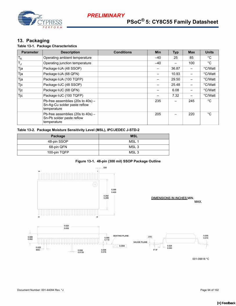
PRELIMINARYPSoC® 5: CY8C55 Family Datasheet
Document Number: 001-44094 Rev. *J Page 94 of 102
13. Packaging
Figure 13-1. 48-pin (300 mil) SSOP Package Outline
Table 13-1. Package Characteristics
Parameter Description Conditions Min Typ Max Units
TA Operating ambient temperature –40 25 85 °C
TJ Operating junction temperature –40 – 100 °C
Tja Package JA (48 SSOP) – 36.87 – °C/Watt
Tja Package JA (68 QFN) – 10.93 – °C/Watt
Tja Package JA (100 TQFP) – 29.50 – °C/Watt
Tjc Package JC (48 SSOP) – 25.48 – °C/Watt
Tjc Package JC (68 QFN) – 6.08 – °C/Watt
Tjc Package JC (100 TQFP) – 7.32 – °C/Watt
Pb-free assemblies (20s to 40s) – Sn-Ag-Cu solder paste reflow temperature
235 – 245 °C
Pb-free assemblies (20s to 40s) – Sn-Pb solder paste reflow temperature
205 – 220 °C
Table 13-2. Package Moisture Sensitivity Level (MSL), IPC/JEDEC J-STD-2
Package MSL
48-pin SSOP MSL 1
68-pin QFN MSL 3
100-pin TQFP MSL 3
001-09618 *C
0.095
0.0250.008
SEATING PLANE
0.420
0.088
.020
0.2920.299
0.395
0.092
BSC
0.110
0.016
0.620
0.0080.0135
0.630
DIMENSIONS IN INCHES MIN.MAX.
0.0400.024
0°-8°
GAUGE PLANE
.010
124
25 48
0.004
0.0050.010
[+] Feedback [+] Feedback [+] Feedback [+] Feedback

PRELIMINARYPSoC® 5: CY8C55 Family Datasheet
Document Number: 001-44094 Rev. *J Page 95 of 102
Figure 13-2. 68-pin QFN 8x8 with 0.4 mm Pitch Package Outline (Sawn Version)
Figure 13-3. 100-pin TQFP (14 x 14 x 1.4 mm) Package Outline
TOP VIEW
0.200 REF
PIN 1 DOTLASER MARK
18
34
35
51
52
68
1
17
0.08
CSE
ATIN
G P
LAN
E
0.05 MAX
1. HATCH AREA IS SOLDERABLE EXPOSED METAL.
2. REFERENCE JEDEC#: MO-220
4. ALL DIMENSIONS ARE IN MILLIMETERS
NOTES:
3. PACKAGE WEIGHT: 0.17g
BOTTOM VIEW
1
0.400±0.100
0.400 PITCH
68
52
51
35
34
18
17
8.00
0±0.
100
8.000±0.100
0.900±0.100
6.40
REF
6.40 REF
SIDE VIEW
0.20±0.05
5.7±0.10
PAD EXPOSED
SOLDERABLE
5.7±0.10
PIN1 IDR 0.20
001-09618 *C
0.22
±0.0
5
0.50
14.00±0.05 SQ
16.00±0.25 SQ
1.40±0.05
12°±1°
1.60 MAX.
0.05 MIN.
0.60±0.15
0° MIN.
0.25
0°-7°
(8X)
STAND-OFF
R 0.08 MIN.
TYP.
GAUGE PLANE
0.20 MAX.
0.15 MAX.
0.20 MAX.
1
100
R 0.08 MIN.0.20 MAX.
76
75
5125
26 50
0 0 12.0000
0.08
SEE DETAIL A
DETAIL A
SEATING PLANE
NOTE: PKG. CAN HAVE
OR
TOP LEFT CORNER CHAMFER 4 CORNERS CHAMFER
NOTE:
1. JEDEC STD REF MS-0262. BODY LENGTH DIMENSION DOES NOT INCLUDE MOLD PROTRUSION/END FLASH
MOLD PROTRUSION/END FLASH SHALL NOT EXCEED 0.0098 in (0.25 mm) PER SIDE
3. DIMENSIONS IN MILLIMETERSBODY LENGTH DIMENSIONS ARE MAX PLASTIC BODY SIZE INCLUDING MOLD MISMATCH
51-85048-*D
[+] Feedback [+] Feedback [+] Feedback [+] Feedback

PRELIMINARYPSoC® 5: CY8C55 Family Datasheet
Document Number: 001-44094 Rev. *J Page 96 of 102
14. Acronyms
Table 14-1. Acronyms Used in this Document
Acronym Description
abus analog local bus
ADC analog-to-digital converter
AG analog global
AHB AMBA (advanced microcontroller bus archi-tecture) high-performance bus, an ARM data transfer bus
ALU arithmetic logic unit
AMUXBUS analog multiplexer bus
API application programming interface
APSR application program status register
ARM® advanced RISC machine, a CPU architecture
ATM automatic thump mode
BW bandwidth
CAN Controller Area Network, a communications protocol
CMRR common-mode rejection ratio
CPU central processing unit
CRC cyclic redundancy check, an error-checking protocol
DAC digital-to-analog converter, see also IDAC, VDAC
DFB digital filter block
DIO digital input/output, GPIO with only digital capabilities, no analog. See GPIO.
DMA direct memory access, see also TD
DNL differential nonlinearity, see also INL
DR port write data registers
DRES digital logic reset
DSI digital system interconnect
DWT data watchpoint and trace
ECC error correcting code
ECO external crystal oscillator
EEPROM electrically erasable programmable read-only memory
EMI electromagnetic interference
EMIF external memory interface
EOC end of conversion
EOF end of frame
EPSR execution program status register
ESD electrostatic discharge
ETM embedded trace macrocell
FIR finite impulse response, see also IIR
FPB flash patch and breakpoint
FS full-speed
GPIO general-purpose input/output, applies to a PSoC pin
HVI high-voltage interrupt, see also LVI, LVD
IC integrated circuit
IDAC current DAC, see also DAC, VDAC
IDE integrated development environment
I2C, or IIC Inter-Integrated Circuit, a communications protocol
IIR infinite impulse response, see also FIR
ILO internal low-speed oscillator, see also IMO
IMO internal main oscillator, see also ILO
INL integral nonlinearity, see also DNL
I/O input/output, see also GPIO, DIO, SIO, USBIO
IPOR initial power-on reset
IPSR interrupt program status register
IRQ interrupt request
ITM instrumentation trace macrocell
LCD liquid crystal display
LIN Local Interconnect Network, a communications protocol.
LR link register
LUT lookup table
LVD low-voltage detect, see also LVI
LVI low-voltage interrupt, see also HVI
LVTTL low-voltage transistor-transistor logic
MAC multiply-accumulate
MCU microcontroller unit
MISO master-in slave-out
NC no connect
NMI nonmaskable interrupt
NRZ non-return-to-zero
NVIC nested vectored interrupt controller
NVL nonvolatile latch, see also WOL
opamp operational amplifier
PAL programmable array logic, see also PLD
PC program counter
PCB printed circuit board
PGA programmable gain amplifier
Table 14-1. Acronyms Used in this Document (continued)
Acronym Description
[+] Feedback [+] Feedback [+] Feedback [+] Feedback

PRELIMINARYPSoC® 5: CY8C55 Family Datasheet
Document Number: 001-44094 Rev. *J Page 97 of 102
15. Reference Documents
PSoC® 3, PSoC® 5 Architecture TRM
PSoC® 5 Registers TRM
PHUB peripheral hub
PHY physical layer
PICU port interrupt control unit
PLA programmable logic array
PLD programmable logic device, see also PAL
PLL phase-locked loop
PMDD package material declaration datasheet
POR power-on reset
PRES precise power-on reset
PRS pseudo random sequence
PS port read data register
PSoC® Programmable System-on-Chip™
PSRR power supply rejection ratio
PWM pulse-width modulator
RAM random-access memory
RISC reduced-instruction-set computing
RMS root-mean-square
RTC real-time clock
RTL register transfer language
RTR remote transmission request
RX receive
SAR successive approximation register
SC/CT switched capacitor/continuous time
SCL I2C serial clock
SDA I2C serial data
S/H sample and hold
SIO special input/output, GPIO with advanced features. See GPIO.
SNR signal-to-noise ratio
SOC start of conversion
Table 14-1. Acronyms Used in this Document (continued)
Acronym Description
SOF start of frame
SPI Serial Peripheral Interface, a communications protocol
SR slew rate
SRAM static random access memory
SRES software reset
SWD serial wire debug, a test protocol
SWV single-wire viewer
TD transaction descriptor, see also DMA
THD total harmonic distortion
TIA transimpedance amplifier
TRM technical reference manual
TTL transistor-transistor logic
TX transmit
UART Universal Asynchronous Transmitter Receiver, a communications protocol
UDB universal digital block
USB Universal Serial Bus
USBIO USB input/output, PSoC pins used to connect to a USB port
VDAC voltage DAC, see also DAC, IDAC
WDT watchdog timer
WOL write once latch, see also NVL
WRES watchdog timer reset
XRES external reset I/O pin
XTAL crystal
Table 14-1. Acronyms Used in this Document (continued)
Acronym Description
[+] Feedback [+] Feedback [+] Feedback [+] Feedback
PRELIMINARYPSoC® 5: CY8C55 Family Datasheet
Document Number: 001-44094 Rev. *J Page 98 of 102
16. Document Conventions
16.1 Units of Measure
Table 16-1. Units of Measure
Symbol Unit of Measure
°C degrees Celsius
dB decibels
fF femtofarads
Hz hertz
KB 1024 bytes
kbps kilobits per second
Khr kilohours
kHz kilohertz
k kilohms
ksps kilosamples per second
LSB least significant bit
Mbps megabits per second
MHz megahertz
M megaohms
Msps megasamples per second
µA microamperes
µF microfarads
µH microhenrys
µs microseconds
µV microvolts
µW microwatts
mA milliamperes
ms milliseconds
mV millivolts
nA nanoamperes
ns nanoseconds
nV nanovolts
ohms
pF picofarads
ppm parts per million
ps picoseconds
s seconds
sps samples per second
sqrtHz square root of hertz
V volts
[+] Feedback [+] Feedback [+] Feedback [+] Feedback

PRELIMINARYPSoC® 5: CY8C55 Family Datasheet
Document Number: 001-44094 Rev. *J Page 99 of 102
17. Revision History
Description Title: PSoC® 5: CY8C55 Family Datasheet Programmable System-on-Chip (PSoC®)Document Number: 001-44094
Rev. ECN No. Submission Date
Orig. of Change Description of Change
** 2517856 17/06/08 DSG New datasheet for new device CY8C55 Family Datasheet.
*A 2611826 11/24/08 GDK Reorganized content to be consistent with the TRMAdded section on DAC. Updated Boost Converter section. Updated Conversion Signals section. Classified Ordering Information according to CPU speed; added information on security features and ROHS complianceAdded a section on XRES Specifications under Electrical SpecificationUpdated Analog Subsystem and CY8C55 Architecture block diagramsUpdated Electrical Specifications section
*B 2707147 05/15/09 GDK/MKEA Updates to Electrical Specifications. Renamed CyDesigner as PSoC CreatorAdded Analog Routing section. Content edits
*C 2759055 09/02/09 MKEA Updated Part Numbering Conventions. Added Section 11.7.5 (EMIF Figures and Tables). Updated GPIO and SIO AC specifications. Updated XRES Pin Description and Xdata Address Map specifications. Updated DFB and Comparator specifications. Updated PHUB features section and RTC in sleep mode. Updated IDAC and VDAC DC and Analog Global SpecificationsUpdated USBIO AC and Delta Sigma ADC specifications. Updated PPOR and Voltage Monitors DC specifications. Updated Drive Mode diagramUpdated Analog Comparator and System diagramsOther edits to electrical specifications
*D 2824626 12/09/09 MKEA Updated I2C section to reflect 1 Mbps. Updated Table 11-6 and 11- 7 (Boost AC and DC specs); also added Shottky Diode specs. Changed current for sleep/hibernate mode to include SIO; Added footnote to analog global specs.Updated Figures 1-1, 6-2, 7-14, and 8-1. Updated Table 6-2 and Table 6-3 (Hibernate and Sleep rows) and Power Modes section. Updated GPIO and SIO AC specifications. Updated Gain error in IDAC and VDAC specifications. Updated description of VDDA spec in Table 11-1 and removed GPIO Clamp Current parameter. Moved FILO from ILO DC to AC table. Added PCB Layout and PCB Schematic diagrams. Updated Fgpioout spec (Table 11-9). Added duty cycle frequency in PLL AC spec table. Added note for Sleep and Hibernate modes and Active Mode specs in Table 11-2. Linked URL in Section 10.3 to PSoC Creator site. Updated Ja and Jc values in Table 13-1. Updated Single Sample Mode and Fast FIR Mode sections. Updated Input Resistance specification in Del-Sig ADC table. Added Tio_init parameter. Updated PGA and UGB AC Specs. Removed SPC ADC. Updated Boost Converter section.Added section 'SIO as Comparator'; updated Hysteresis spec (differential mode) in Table 11-10. Updated VBAT condition and deleted Vstart parameter in Table 11-6. Removed reference to Idle mode. CDT 59671: Updated footnotes and ADC column in ordering information. Removed CSA (Section 8.7). Updated IMO table and number of UDBs
*E 2873520 02/04/10 MKEA Changed maximum value of PPOR_TR to '1'. Updated VBIAS specification. Updated Figure 8-1 and Figure 6-3. Updated Interrupt Vector table, Updated Sales links. Updated JTAG and SWD specifications. Removed Jp-p and Jperiod from ECO AC Spec table. Added note on sleep timer in Table 11-2. Updated ILO AC and DC specifications. Added Resolution parameter in VDAC and IDAC tables. Updated IOUT typical and maximum values. Changed Temperature Sensor range to -40 °C to +85 °C. Removed Latchup specification from Table 11-1
[+] Feedback [+] Feedback [+] Feedback [+] Feedback

PRELIMINARYPSoC® 5: CY8C55 Family Datasheet
Document Number: 001-44094 Rev. *J Page 100 of 102
*F 2911720 04/13/10 MKEA Updated Vb pin in PCB Schematic. Updated Tstartup parameter in AC Specifications table. Added Load regulation and Line regulation parameters to Inductive Boost Regulator DC Specifications table. Updated ICC parameter in LCD Direct Drive DC Specs table. In page 1, updated internal oscillator range under Precision programmable clocking to start from 3 MHz. Updated IOUT parameter in LCD Direct Drive DC Specs table. Updated Table 6-2 and Table 6-3. Added bullets on CapSense in page 1; added CapSense column in Section 12. Removed some references to footnote [1]. Added footnote in PLL AC Specification table.Added PLL intermediate frequency row with footnote in PLL AC Specs table. Added UDBs subsection under 11.6 Digital Peripherals. Updated Figure 2-6 (PCB Layout). Updated Pin Descriptions section and modified Figures 6-6, 6-8, 6-9. Updated LVD in Tables 6-2 and 6-3; modified Low power modes bullet in page 1. Added note to Figures 2-5 and 6-2; Updated Figure 6-2 to add capacitors for VDDA and VDDD pins. Updated boost converter section (6.2.2). Updated Tstartup values in Table 11-3. Removed IPOR rows from Table 11-68. Updated 6.3.1.1, Power Voltage Level Monitors. Updated section 5.2 and Table 11-2 to correct suggestion of execution from flash. Updated VREF specs in Table 11-21. Updated IDAC uncompensated gain error in Table 11-25. Added sentence to last paragraph of section 6.1.1.3. Updated TRESP, high and low power modes, in Table 11-24. Updated f_TCK values in Table 11-73 and f_SWDCK values in Table 11-74.Updated SNR condition in Table 11-20. Corrected unit of measurement in Table 11-21.Updated sleep wakeup time in Table 6-3 and Tsleep in Table 11-3. Added 1.71 V <= VDDD < 3.3 V, SWD over USBIO pins value to Table 11-74.Removed mention of hibernate reset (HRES) from page 1 features, Table 6-3, Section 6.2.1.4, Section 6.3, and Section 6.3.1.1. Changed PPOR/PRES to TBDs in Section 6.3.1.1, Section 6.4.1.6 (changed PPOR to reset), Table 11-3 (changed PPOR to PRES), Table 11-68 (changed title, values TBD), and Table 11-69 (changed PPOR_TR to PRES_TR).Added sentence saying that LVD circuits can generate a reset to Section 6.3.1.1. Changed IDD values on page 1, page 5, and Table 11-2.Changed resume time value in Section 6.2.1.3. Changed ESD HBM value in Table 11-1. Changed SNR in 16-bit resolution mode value and sample rate row in Table 11-20. Removed VDDA = 1.65 V rows and changed BWag value in Table 11-22.Changed VIOFF values and changed CMRR value in Table 11-23. Changed INL max value in Table 11-27. Added max value to the Quiescent current specs in Tables 11-29 and 11-31.Changed occurrences of “Block” to “Row” and deleted the “ECC not included” footnote in Table 11-57. Changed max response time value in Tables 11-69 and 11-71. Changed the Startup time in Table 11-79. Added condition to intermediate frequency row in Table 11-85.Added row to Table 11-69.Added brown out note to Section 11.8.1.
Description Title: PSoC® 5: CY8C55 Family Datasheet Programmable System-on-Chip (PSoC®)Document Number: 001-44094
[+] Feedback [+] Feedback [+] Feedback [+] Feedback

PRELIMINARYPSoC® 5: CY8C55 Family Datasheet
Document Number: 001-44094 Rev. *J Page 101 of 102
*G 2936486 05/24/10 MKEA Replaced VDDIO with VDDD in USBIO diagram and specification tables, added text in USBIO section of Electrical Specifications. Added Table 13-2 (Package MSL)Modified Tstorag condition and changed maximum value to 100Added bullet (Pass) in ALU (section 7.2.2.2)Added figures for kHzECO and MHzECO in the External Oscillator sectionUpdated Figure 6-1(Clocking Subsystem diagram)Resolved discrepancies with the EROS in Electrical Specifications sectionsUpdated PSoC Creator Framework imageUpdated SIO DC Specifications (VIH and VIL parameters)Updated values in Low power modes bullet on page 1Updated Figure 8-2Updated PCB Layout and Schematic, updates as per MTRB review commentsUpdated Table 6-3 (power changed to current)In 32kHZ EC DC Specifications table, changed ICC Max to 0.25In IMO DC Specifications table, updated Supply Current valuesUpdated GPIO DC Specs tableRemoved all references to 48-SSOP package
*H 2944841 6/4/2010 FSU Minor update to post to cypress.com.
*I 2960407 06/24/10 MKEA Corrected typo in Table 11-3 (V/ms to V/ns) and Tables 11-31 and 11-33 (µA to mA)
*J 3019464 08/31/10 MKEA Added USBIO 22 ohm DP and DM resistors to Simplified Block DiagramINL max is changed from 16 to 32 in Table 11-20, 20-Bit Delta-Sigma ADC AC Specifications. Added to Table 6-6 a footnote and references to same.Added sentences to the resistive pull up and pull down description bullets.Added sentence to Section 6.4.11, Adjustable Output Level.Updated section 5.5 External Memory Interface Updated Table 11-73 JTAG Interface AC Specifications Updated Table 11-74 SWD Interface AC SpecificationsA footnote, TRACEPORT / TRACECLK max frequency is limited by GPIO max frequency, is added to the section 11.8.6. 48-SSOP package added.
Description Title: PSoC® 5: CY8C55 Family Datasheet Programmable System-on-Chip (PSoC®)Document Number: 001-44094
[+] Feedback [+] Feedback [+] Feedback [+] Feedback

Document Number: 001-44094 Rev. *J Revised September 2, 2010 Page 102 of 102
CapSense®, PSoC®3, PSoC®5, and PSoC® Creator™ are trademarks and PSoC® is a registered trademark of Cypress Semiconductor Corp. All other trademarks or registered trademarks referenced herein are property of the respective corporations.
Purchase of I2C components from Cypress or one of its sublicensed Associated Companies conveys a license under the Philips I2C Patent Rights to use these components in an I2C system, provided that the system conforms to the I2C Standard Specification as defined by Philips.
ARM is a registered trademark, and Keil, and RealView are trademarks, of ARM Limited. All products and company names mentioned in this document may be the trademarks of their respective holders.
PRELIMINARY
PSoC® 5: CY8C55 Family Datasheet
© Cypress Semiconductor Corporation, 2006-2010. The information contained herein is subject to change without notice. Cypress Semiconductor Corporation assumes no responsibility for the use of any circuitry other than circuitry embodied in a Cypress product. Nor does it convey or imply any license under patent or other rights. Cypress products are not warranted nor intended to be used for medical, life support, life saving, critical control or safety applications, unless pursuant to an express written agreement with Cypress. Furthermore, Cypress does not authorize its products for use as critical components in life-support systems where a malfunction or failure may reasonably be expected to result in significant injury to the user. The inclusion of Cypress products in life-support systems application implies that the manufacturer assumes all risk of such use and in doing so indemnifies Cypress against all charges.
Any Source Code (software and/or firmware) is owned by Cypress Semiconductor Corporation (Cypress) and is protected by and subject to worldwide patent protection (United States and foreign), United States copyright laws and international treaty provisions. Cypress hereby grants to licensee a personal, non-exclusive, non-transferable license to copy, use, modify, create derivative works of, and compile the Cypress Source Code and derivative works for the sole purpose of creating custom software and or firmware in support of licensee product to be used only in conjunction with a Cypress integrated circuit as specified in the applicable agreement. Any reproduction, modification, translation, compilation, or representation of this Source Code except as specified above is prohibited without the express written permission of Cypress.
Disclaimer: CYPRESS MAKES NO WARRANTY OF ANY KIND, EXPRESS OR IMPLIED, WITH REGARD TO THIS MATERIAL, INCLUDING, BUT NOT LIMITED TO, THE IMPLIED WARRANTIES OF MERCHANTABILITY AND FITNESS FOR A PARTICULAR PURPOSE. Cypress reserves the right to make changes without further notice to the materials described herein. Cypress does not assume any liability arising out of the application or use of any product or circuit described herein. Cypress does not authorize its products for use as critical components in life-support systems where a malfunction or failure may reasonably be expected to result in significant injury to the user. The inclusion of Cypress’ product in a life-support systems application implies that the manufacturer assumes all risk of such use and in doing so indemnifies Cypress against all charges.
Use may be limited by and subject to the applicable Cypress software license agreement.
Sales, Solutions, and Legal Information
Worldwide Sales and Design Support
Cypress maintains a worldwide network of offices, solution centers, manufacturer’s representatives, and distributors. To find the office closest to you, visit us at Cypress Locations.
Products
Automotive cypress.com/go/automotive
Clocks & Buffers cypress.com/go/clocks
Interface cypress.com/go/interface
Lighting & Power Control cypress.com/go/powerpsoc
cypress.com/go/plc
Memory cypress.com/go/memory
Optical & Image Sensing cypress.com/go/image
PSoC cypress.com/go/psoc
Touch Sensing cypress.com/go/touch
USB Controllers cypress.com/go/USB
Wireless/RF cypress.com/go/wireless
PSoC Solutions
psoc.cypress.com/solutions
PSoC 1 | PSoC 3 | PSoC 5
[+] Feedback [+] Feedback [+] Feedback [+] Feedback