Embed Size (px)
Citation preview
PRELIMINARY PSoC® 6 MCU: PSoC 62Datasheet
Programmable System-on-Chip (PSoC®)
Cypress Semiconductor Corporation • 198 Champion Court • San Jose, CA 95134-1709 • 408-943-2600Document Number: 002-18449 Rev. *B Revised September 26, 2017
General Description
PSoC® is a scalable and reconfigurable platform architecture for a family of programmable embedded system controllers with ARM®
Cortex™ CPUs (single and multi-core). The PSoC 6 product family, based on an ultra low-power 40-nm platform, is a combination ofa dual-core microcontroller with low-power Flash technology and digital programmable logic, high-performance analog-to-digital anddigital-to-analog conversion, low-power comparators, and standard communication and timing peripherals.
Features32-bit Dual Core CPU Subsystem
150-MHz ARM Cortex-M4F CPU with single-cycle multiply(Floating Point and Memory Protection Unit)
100-MHz Cortex M0+ CPU
User-selectable core logic operation at either 1.1 V or 0.9 V
Inter-processor communication supported in hardware
8 KB 4-way set-associative Instruction Caches for the M4 andM0+ CPUs respectively
Active CPU power consumption slope with 1.1-V core operationfor the Cortex M4 is 40 µA/MHz and 20 µA/MHz for the CortexM0+, both at 3.3-V chip supply voltage with the internal buckregulator
Active CPU power consumption slope with 0.9-V core operationfor the Cortex M4 is 26 µA/MHz and 17 µA/MHz for the CortexM0+, both at 3.3-V chip supply voltage with the internal buckregulator
Two DMA controllers with 16 channels each
Flexible Memory Sub-system
1 MB Application Flash with 32-KB EEPROM area and 32-KBSecure Flash
128-bit wide Flash accesses reduce power
Flash Read-While-Write (RWW) allows updating the Flashwhile executing from it
SRAM with Selectable Retention Granularity
288-KB integrated SRAM
32-KB retention boundaries (can retain 32K to 288K in 32Kincrements)
One-Time-Programmable (OTP) E-Fuse memory for validationand security
Low-Power 1.7-V to 3.6-V Operation
Active, Low-power Active, Sleep, Low-power Sleep, DeepSleep, and Hibernate modes for fine-grained powermanagement
Deep Sleep mode current with 64K SRAM retention is 7 µAwith 3.3 V external supply and internal buck
On-chip Single-In Multiple Out (SIMO) DC-DC Buck converter,<1 µA quiescent current
Backup domain with 64 bytes of memory and Real-Time-Clock
Flexible Clocking Options
On-chip crystal oscillators (High-speed, 4 to 33 MHz, andWatch crystal, 32 kHz)
Phase-locked Loop (PLL) for multiplying clock frequencies
8 MHz Internal Main Oscillator (IMO) with 1% accuracy
Ultra low-power 32-kHz Internal Low-speed Oscillator (ILO)with 10% accuracy
IMO can be locked to 32 kHz WCO input for better accuracy
Frequency Locked Loop (FLL) for multiplying IMO frequency
Serial Communication
Nine independent run-time reconfigurable serial communi-cation blocks (SCBs), each is software configurable as I2C,SPI, or UART
USB Full-Speed Dual-role Host and Device interface
Timing and Pulse-Width Modulation
Thirty-two 16-bit Timer/Counter Pulse-Width Modulator(TCPWM) blocks
Center-aligned, Edge, and Pseudo-random modes
Comparator-based triggering of Kill signals
Up to 104 Programmable GPIOs
Drive modes, strengths, and slew rates are programmable
Six overvoltage tolerant (OVT) pins
Packages
124-BGA
80-WLCSP
Audio Subsystem
I2S Interface; up to 192 kilosamples Word Clock
Two PDM channels for stereo digital microphones
QSPI Interface
Execute-In-Place (XIP) from external Quad SPI Flash
On-the-fly encryption and decryption
4 KB QSPI cache for greater XIP performance with lower power
Supports 1, 2, 4, and Dual-Quad interfaces
Errata: For information on silicon errata, see “Errata” on page 56. Details include trigger conditions, devices affected, and proposed workaround.
Document Number: 002-18449 Rev. *B Page 2 of 61
PRELIMINARYPSoC® 6 MCU: PSoC 62
Datasheet
Programmable Analog
12-bit 1 Msps SAR ADC with differential and single-endedmodes and 16-Channel Sequencer with signal averaging
One 12-bit voltage mode DAC with < 5-µs settling time
Two opamps with low-power operation modes
Two low-power comparators that operate in Deep Sleep andHibernate modes.
Built-in temp sensor connected to ADC
Programmable Digital
12 programmable logic blocks, each with 8 Macrocells and an8-bit data path (called universal digital blocks or UDBs)
Usable as drag-and-drop Boolean primitives (gates, registers),or as Verilog programmable blocks
Cypress-provided peripheral component library using UDBswith common functions such as SDIO, CommunicationPeripherals such as LIN, UART, SPI, I2C, S/PDIF, WaveformGenerator, Pseudo-Random Sequence (PRS) generation, andmany other functions.
Smart I/O (Programmable I/O) blocks enable Booleanoperations on signals coming from, and going to, GPIO pins
Two ports with Smart_IO blocks, capability are provided; theseare available during Deep Sleep
Capacitive Sensing
Cypress Capacitive Sigma-Delta (CSD) provides best-in-classSNR, liquid tolerance, and proximity sensing
Mutual Capacitance sensing (Cypress CSX) with dynamicusage of both Self and Mutual sensing
Wake on Touch with very low current
Cypress-supplied software component makes capacitivesensing design fast and easy
Automatic hardware tuning (SmartSense™)
Energy Profiler
Block that provides history of time spent in different powermodes
Allows software energy profiling to observe and optimizeenergy consumption
PSoC Creator Design Environment
Integrated Development Environment provides schematicdesign entry and build (with analog and digital automaticrouting) and code development and debugging
Applications Programming Interface (API Component) for allfixed-function and programmable peripherals
Industry-Standard Tool Compatibility
After schematic entry, development can be done withARM-based industry-standard development tools
Configure in PSoC Creator and export to ARM/Keil or IAR IDEsfor code development and debugging
Supports industry standard ARM Trace Emulation TraceModule
Security Built into Platform Architecture
Multi-faceted secure architecture based on ROM-based root oftrust
Secure Boot uninterruptible until system protection attributesare established
Authentication during boot using hardware hashing
Step-wise authentication of execution images
Secure execution of code in execute-only mode for protectedroutines
All Debug and Test ingress paths can be disabled
Cryptography Accelerators
Hardware acceleration for Symmetric and Asymmetriccryptographic methods (AES, 3DES, RSA, and ECC) and Hashfunctions (SHA-512, SHA-256)
True Random Number Generator (TRNG) function
Document Number: 002-18449 Rev. *B Page 3 of 61
PRELIMINARYPSoC® 6 MCU: PSoC 62
Datasheet
Contents
Blocks and Functionality ................................................. 4Functional Definition........................................................ 5
CPU and Memory Subsystem ..................................... 5System Resources ...................................................... 5Analog Blocks.............................................................. 6Programmable Digital.................................................. 7Fixed-Function Digital.................................................. 7GPIO ........................................................................... 7Special-Function Peripherals ...................................... 8
Pinouts .............................................................................. 9Power............................................................................... 22Development Support .................................................... 24
Documentation .......................................................... 24Online ........................................................................ 24Tools.......................................................................... 24
Electrical Specifications ................................................ 25Absolute Maximum Ratings....................................... 25Device-Level Specifications ...................................... 25Analog Peripherals .................................................... 30
Digital Peripherals ..................................................... 38Memory ..................................................................... 40System Resources .................................................... 41
Ordering Information...................................................... 48Packaging........................................................................ 50Acronyms........................................................................ 53Document Conventions ................................................. 55
Units of Measure ....................................................... 55Errata ............................................................................... 56PSoC 6X Qualification Status ........................................ 56PSoC 6X Errata Summary.............................................. 56Revision History ............................................................. 60Sales, Solutions, and Legal Information ...................... 61
Worldwide Sales and Design Support....................... 61Products .................................................................... 61PSoC® Solutions ...................................................... 61Cypress Developer Community................................. 61Technical Support ..................................................... 61
Document Number: 002-18449 Rev. *B Page 4 of 61
PRELIMINARYPSoC® 6 MCU: PSoC 62
Datasheet
Blocks and Functionality
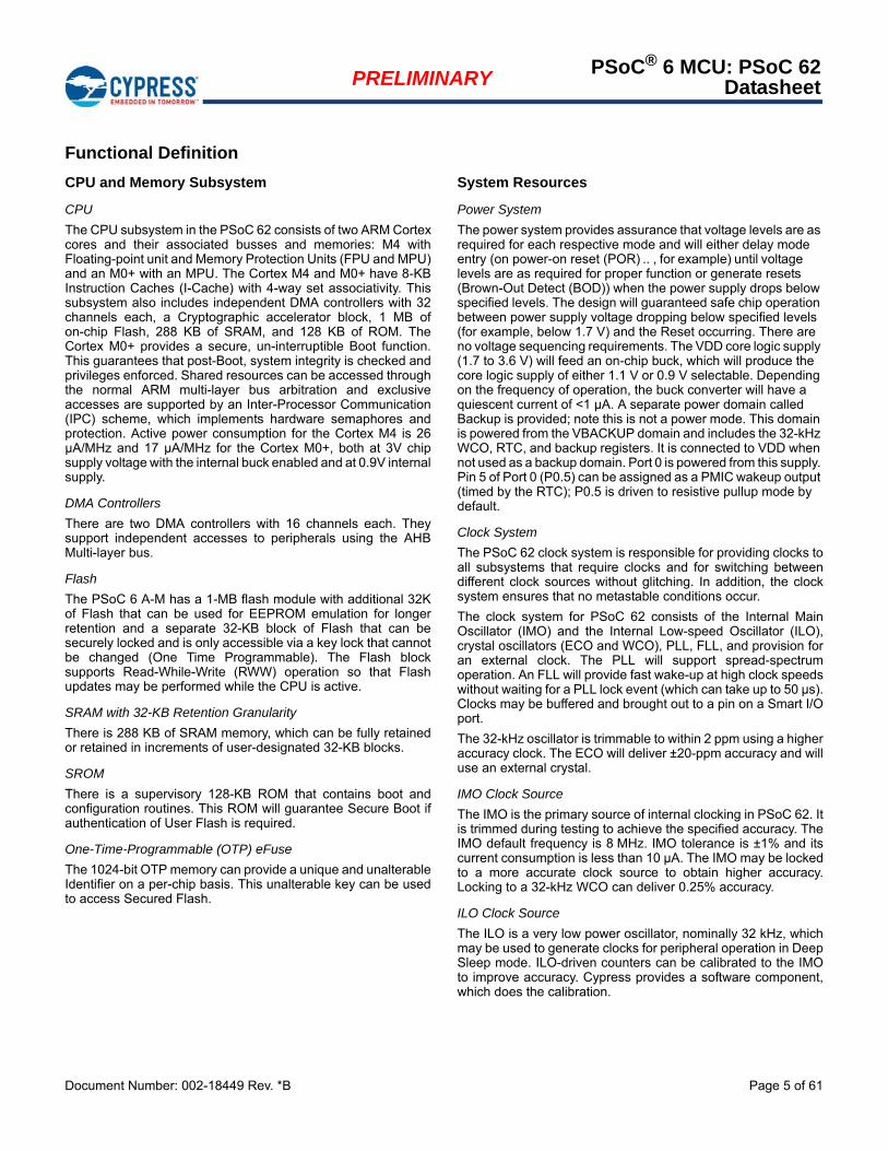
The PSoC 62 block diagram is shown in Figure 1. There are four major subsystems: CPU subsystem, System resources, peripheralblocks, and I/O subsystem.
Figure 1. Block Diagram
Figure 1 shows the subsystems of the chip and gives a very simplified view of their inter-connections (Multi-layer AHB is used inpractice). The color-coding shows the lowest power mode where the particular block is still functional (for example, LP Comparatoris functional in Deep Sleep mode).
PSoC 62 devices include extensive support for programming, testing, debugging, and tracing both hardware and firmware.
Complete debug-on-chip functionality enables full device debugging in the final system using the standard production device. It doesnot require special interfaces, debugging pods, simulators, or emulators. Only the standard programming connections are requiredto fully support debug.
The PSoC Creator Integrated Development Environment (IDE) provides fully integrated programming and debug support for PSoC 62devices. The SWJ (SWD and JTAG) interface is fully compatible with industry-standard third party probes. With the ability to disabledebug features, with very robust flash protection, and by allowing customer-proprietary functionality to be implemented in on-chipprogrammable blocks, the PSoC 62 family provides a very high level of security.
The debug circuits are enabled by default and can only be disabled in firmware. If not enabled, the only way to re-enable them is toerase the entire device, clear flash protection, and reprogram the device with new firmware that enables debugging.
Additionally, all device interfaces can be permanently disabled (device security) for applications concerned about phishing at-tacksdue to a maliciously reprogrammed device or attempts to defeat security by starting and interrupting flash programming sequences.All programming, debug, and test interfaces are disabled when maximum device security is enabled. The security level is a trade-offthe customer can make.
CPU Subsystem
System Interconnect (Multi Layer AHB, MPU/SMPU, IPC)
ROM128 KB
ROM Controller
CRYPTODES/TDES,
AES,SHA,CRC,TRNG,RSA/ECC
Accelerator
Initiator/MMIO
SWJ/MTB/CTI
8KB Cache
Cortex M0+100 MHz (1.1V)25 MHz (0.9V)MUL, NVIC, MPU
IO Subsystem
Peripheral Interconnect (MMIO, PPU)
IOS
S G
PIO
PCLK
104 GPIOs (6 of these are OVT Pins)
EF
US
E (
1024
bits
)
PSoC 62
Ser
ial M
emor
y I/F
(QS
PI
with
OT
F E
ncr
yptio
n/D
ecry
ptio
n))
DMAMMIO
US
B-F
SH
ost +
De
vice
FS
/LS
PH
Y
FLASH1024+32 KB
FLASH Controller
SWJ/ETM/ITM/CTI
FPU, NVIC, MPU, BB
Cortex M4150 MHz (1.1V)50 MHz (0.9V)
8KB Cache
SRAM9x 32 KB
SRAM Controller
Ene
rgy
Pro
filer
x12
UDB...
ProgrammableDigital
UDB
8x S
eria
l Com
m(I
2C,S
PI,U
AR
T,L
IN,S
MC
)
Cap
Sen
se
32x
TC
PW
M(T
IME
R,C
TR
,QD
, PW
M)
1x S
eria
l Com
m(I
2C,S
PI,
De
ep S
lee
p)
DAC(12-bit)
SAR ADC(12-bit)
x1
CTB/CTBm
x12x OpAmp
ProgrammableAnalog
x1
SARMUX
LP C
ompa
rato
r
Port Interface & Digital System Interconnect (DSI)
High Speed I/O Matrix, Smart I/O, Boundary Scan
I2S
Mas
ter/
Sla
ve
PD
M/P
CM
AudioSubsystem
LC
D
DataWire/DMA
2x 16 Ch
Initiator/MMIO
WCORTC
BREG
BackupBackup Control
Digital DFT
Test
Analog DFT
System Resources
Power
Reset
Sleep Control
PWRSYS-LP/ULP
REF
Reset Control
TestMode Entry
XRES
DeepSleepHibernate
Power Modes
Backup
Active/SleepLowePowerActive/Sleep
Buck
PORLVDBOD
OVP
ClockClock Control
IMOWDT
CSV1xPLL
ECOILO
FLL
Document Number: 002-18449 Rev. *B Page 5 of 61
PRELIMINARYPSoC® 6 MCU: PSoC 62
Datasheet
Functional Definition
CPU and Memory Subsystem
CPU
The CPU subsystem in the PSoC 62 consists of two ARM Cortexcores and their associated busses and memories: M4 withFloating-point unit and Memory Protection Units (FPU and MPU)and an M0+ with an MPU. The Cortex M4 and M0+ have 8-KBInstruction Caches (I-Cache) with 4-way set associativity. Thissubsystem also includes independent DMA controllers with 32channels each, a Cryptographic accelerator block, 1 MB ofon-chip Flash, 288 KB of SRAM, and 128 KB of ROM. TheCortex M0+ provides a secure, un-interruptible Boot function.This guarantees that post-Boot, system integrity is checked andprivileges enforced. Shared resources can be accessed throughthe normal ARM multi-layer bus arbitration and exclusiveaccesses are supported by an Inter-Processor Communication(IPC) scheme, which implements hardware semaphores andprotection. Active power consumption for the Cortex M4 is 26µA/MHz and 17 µA/MHz for the Cortex M0+, both at 3V chipsupply voltage with the internal buck enabled and at 0.9V internalsupply.
DMA Controllers
There are two DMA controllers with 16 channels each. Theysupport independent accesses to peripherals using the AHBMulti-layer bus.
Flash
The PSoC 6 A-M has a 1-MB flash module with additional 32Kof Flash that can be used for EEPROM emulation for longerretention and a separate 32-KB block of Flash that can besecurely locked and is only accessible via a key lock that cannotbe changed (One Time Programmable). The Flash blocksupports Read-While-Write (RWW) operation so that Flashupdates may be performed while the CPU is active.
SRAM with 32-KB Retention Granularity
There is 288 KB of SRAM memory, which can be fully retainedor retained in increments of user-designated 32-KB blocks.
SROM
There is a supervisory 128-KB ROM that contains boot andconfiguration routines. This ROM will guarantee Secure Boot ifauthentication of User Flash is required.
One-Time-Programmable (OTP) eFuse
The 1024-bit OTP memory can provide a unique and unalterableIdentifier on a per-chip basis. This unalterable key can be usedto access Secured Flash.
System Resources
Power System
The power system provides assurance that voltage levels are as required for each respective mode and will either delay mode entry (on power-on reset (POR) .. , for example) until voltage levels are as required for proper function or generate resets (Brown-Out Detect (BOD)) when the power supply drops below specified levels. The design will guaranteed safe chip operation between power supply voltage dropping below specified levels (for example, below 1.7 V) and the Reset occurring. There are no voltage sequencing requirements. The VDD core logic supply (1.7 to 3.6 V) will feed an on-chip buck, which will produce the core logic supply of either 1.1 V or 0.9 V selectable. Depending on the frequency of operation, the buck converter will have a quiescent current of <1 µA. A separate power domain called Backup is provided; note this is not a power mode. This domain is powered from the VBACKUP domain and includes the 32-kHz WCO, RTC, and backup registers. It is connected to VDD when not used as a backup domain. Port 0 is powered from this supply. Pin 5 of Port 0 (P0.5) can be assigned as a PMIC wakeup output (timed by the RTC); P0.5 is driven to resistive pullup mode by default.
Clock System
The PSoC 62 clock system is responsible for providing clocks toall subsystems that require clocks and for switching betweendifferent clock sources without glitching. In addition, the clocksystem ensures that no metastable conditions occur.
The clock system for PSoC 62 consists of the Internal MainOscillator (IMO) and the Internal Low-speed Oscillator (ILO),crystal oscillators (ECO and WCO), PLL, FLL, and provision foran external clock. The PLL will support spread-spectrumoperation. An FLL will provide fast wake-up at high clock speedswithout waiting for a PLL lock event (which can take up to 50 µs).Clocks may be buffered and brought out to a pin on a Smart I/Oport.
The 32-kHz oscillator is trimmable to within 2 ppm using a higheraccuracy clock. The ECO will deliver ±20-ppm accuracy and willuse an external crystal.
IMO Clock Source
The IMO is the primary source of internal clocking in PSoC 62. Itis trimmed during testing to achieve the specified accuracy. TheIMO default frequency is 8 MHz. IMO tolerance is ±1% and itscurrent consumption is less than 10 µA. The IMO may be lockedto a more accurate clock source to obtain higher accuracy.Locking to a 32-kHz WCO can deliver 0.25% accuracy.
ILO Clock Source
The ILO is a very low power oscillator, nominally 32 kHz, whichmay be used to generate clocks for peripheral operation in DeepSleep mode. ILO-driven counters can be calibrated to the IMOto improve accuracy. Cypress provides a software component,which does the calibration.
Document Number: 002-18449 Rev. *B Page 6 of 61
PRELIMINARYPSoC® 6 MCU: PSoC 62
Datasheet
Watchdog Timer
A watchdog timer is implemented in the clock block running fromthe ILO or from the WCO; this allows watchdog operation duringDeep Sleep and generates a watchdog reset if not servicedbefore the timeout occurs. The watchdog reset is recorded in theReset Cause register.
Clock Dividers
Integer and Fractional clock dividers are provided for peripheraluse and timing purposes. The clock dividers are 16 and 24 bitsin length to allow very fine clock control.
Reset
The PSoC 62 can be reset from a variety of sources including asoftware reset. Reset events are asynchronous and guaranteereversion to a known state. The reset cause is recorded in aregister, which is sticky through reset and allows software todetermine the cause of the Reset. An XRES pin is reserved forexternal reset to avoid complications with configuration andmultiple pin functions during power-on or reconfiguration.
Analog Blocks
12-bit SAR ADC
The 12-bit, 1-Msps SAR ADC can operate at a maximum clockrate of 18 MHz and requires a minimum of 18 clocks at thatfrequency to do a 12-bit conversion.
The block functionality is augmented for the user by adding areference buffer to it (trimmable to ±1%) and by providing thechoice of three internal voltage references, VDD, VDD/2, andVREF (nominally 1.024 V), as well as an external referencethrough a GPIO pin. The Sample-and-Hold (S/H) aperture isprogrammable; it allows the gain bandwidth requirements of theamplifier driving the SAR inputs, which determine its settlingtime, to be relaxed if required. System performance will be 65 dBfor true 12-bit precision provided appropriate references areused and system noise levels permit it. To improve the perfor-mance in noisy conditions, it is possible to provide an externalbypass (through a fixed pin location) for the internal referenceamplifier.
The SAR is connected to a fixed set of pins through an 8-inputsequencer. The sequencer cycles through the selected channelsautonomously (sequencer scan) and does so with zero switchingoverhead (that is, the aggregate sampling bandwidth is equal to1 Msps whether it is for a single channel or distributed overseveral channels). The sequencer switching is effected througha state machine or through firmware-driven switching. A featureprovided by the sequencer is the buffering of each channel toreduce CPU interrupt-service requirements. To accommodatesignals with varying source impedances and frequencies, it ispossible to have different sample times programmable for eachchannel. Also, the signal range specification through a pair ofrange registers (low and high range values) is implemented witha corresponding out-of-range interrupt if the digitized valueexceeds the programmed range; this allows fast detection ofout-of-range values without having to wait for a sequencer scanto be completed and the CPU to read the values and check forout-of-range values in software.
The SAR is able to digitize the output of the on-chip temperature sensor for calibration and other temperature-dependent functions. The SAR is not available in Deep Sleep and Hibernate modes as it requires a high-speed clock (up to 18 MHz). The SAR operating range is 1.71 to 3.6 V.
Temperature Sensor
PSoC 62 has an on-chip temperature sensor. This consists of adiode, which is biased by a current source that can be disabledto save power. The temperature sensor is connected to the ADC,which digitizes the reading and produces a temperature value byusing a Cypress-supplied software that includes calibration andlinearization.
12-bit Digital-Analog Converter
There is a 12-bit voltage mode DAC on the chip, which can settlein less than 5 µs. The DAC may be driven by the DMA controllersto generate user-defined waveforms. The DAC output from thechip can either be the resistive ladder output (highly linear nearground) or a buffered output.
Continuous Time Block (CTBm) with Two Opamps
This block consists of two opamps, which have their inputs andoutputs connected to fixed pins and have three power modesand a comparator mode. The outputs of these opamps can beused as buffers for the SAR inputs. The non-inverting inputs ofthese opamps can be connected to either of two pins, thusallowing independent sensors to be used at different times. Thepin selection can be made via firmware. The opamps can be setto one of the four power levels; the lowest level allowingoperation in Deep Sleep mode in order to preserve lower perfor-mance Continuous-Time functionality in Deep Sleep mode. TheDAC output can be buffered through an opamp.
Low-Power Comparators
PSoC 62 has a pair of low-power comparators, which can alsooperate in Deep Sleep and Hibernate modes. This allows theanalog system blocks to be disabled while retaining the ability tomonitor external voltage levels during Deep Sleep and Hibernatemodes. The comparator outputs are normally synchronized toavoid metastability unless operating in an asynchronous powermode (Hibernate) where the system wake-up circuit is activatedby a comparator-switch event.
Document Number: 002-18449 Rev. *B Page 7 of 61
PRELIMINARYPSoC® 6 MCU: PSoC 62
Datasheet
Programmable Digital
Smart I/O
There are two Smart I/O blocks, which allow Boolean operationson signals going to the GPIO pins from the subsystems of thechip or on signals coming into the chip. Operation can besynchronous or asynchronous and the blocks operate inlow-power modes, such as Deep Sleep and Hibernate. Thisallows, for example, detection of logic conditions that canindicate that the CPU should wake up instead of waking up ongeneral I/O interrupts, which consume more power and cangenerate spurious wake-ups.
Universal Digital Blocks (UDBs) and Port Interfaces
The PSoC6 has 12 UDBs; the UDB array also provides aswitched Digital System Interconnect (DSI) fabric that allowssignals from peripherals and ports to be routed to and throughthe UDBs for communication and control.
Fixed-Function Digital
Timer/Counter/PWM Block
The timer/counter/PWM block consists of 32 counters withuser-programmable period length. There is a Capture register torecord the count value at the time of an event (which may be anI/O event), a period register which is used to either stop orauto-reload the counter when its count is equal to the periodregister, and compare registers to generate compare valuesignals which are used as PWM duty cycle outputs. The blockalso provides true and complementary outputs withprogrammable offset between them to allow the use asdeadband programmable complementary PWM outputs. It alsohas a Kill input to force outputs to a predetermined state; forexample, this is used in motor-drive systems when anovercurrent state is indicated and the PWMs driving the FETsneed to be shut off immediately with no time for softwareintervention. There are 8 32-bit counters and 24 16-bit counters.
Serial Communication Blocks (SCB)
PSoC 62 has nine SCBs, which can each implement an I2C,UART, or SPI interface. One SCB will operate in Deep Sleep withan external clock, this SCB will only operate in Slave mode(requires external clock).
I2C Mode: The hardware I2C block implements a fullmulti-master and slave interface (it is capable of multimasterarbitration). This block is capable of operating at speeds of up to1 Mbps (Fast Mode Plus) and has flexible buffering options toreduce the interrupt overhead and latency for the CPU. It alsosupports EzI2C that creates a mailbox address range in thememory of PSoC 62 and effectively reduces the I2C communi-cation to reading from and writing to an array in the memory. Inaddition, the block supports an 8-deep FIFO for receive andtransmit, which, by increasing the time given for the CPU to readthe data, greatly reduces the need for clock stretching caused bythe CPU not having read the data on time. The FIFO mode isavailable in all channels and is very useful in the absence ofDMA.
The I2C peripheral is compatible with I2C Standard-mode,Fast-mode, and Fast-Mode Plus devices as defined in the NXPI2C-bus specification and user manual (UM10204). The I2C busI/O is implemented with GPIO in open-drain modes.
UART Mode: This is a full-feature UART operating at up to1 Mbps. It supports automotive single-wire interface (LIN),infrared interface (IrDA), and SmartCard (ISO7816) protocols, allof which are minor variants of the basic UART protocol. Inaddition, it supports the 9-bit multiprocessor mode that allows theaddressing of peripherals connected over common RX and TXlines. Common UART functions such as parity error, breakdetect, and frame error are supported. An 8-deep FIFO allowsmuch greater CPU service latencies to be tolerated.
SPI Mode: The SPI mode supports full Motorola SPI, TI SecureSimple Pairing (SSP) (essentially adds a start pulse that is usedto synchronize SPI Codecs), and National Microwire (half-duplexform of SPI). The SPI block can use the FIFO and supports anEzSPI mode in which the data interchange is reduced to readingand writing an array in memory. The SPI interface will operatewith a 48-MHz SPI Clock.
USB Full-Speed Dual Role Host and Device interface
The PSoC6 incorporates a dual-role USB Host and Deviceinterface. The device can have up to eight endpoints. A 512-byteSRAM buffer is provided and DMA is supported.
QSPI Interface
A Quad SPI (QSPI) interface (selectable 1, 2, or 4 bits width) isprovided running at 80 MHz. This block also supports on-the-flyencryption and decryption to support Execute-In-Place operationat reasonable speeds.
GPIO
PSoC 62 has up to 104 GPIOs. The GPIO block implements thefollowing:
Eight drive strength modes: Analog input mode (input and output buffers disabled) Input only Weak pull-up with strong pull-down Strong pull-up with weak pull-down Open drain with strong pull-down Open drain with strong pull-up Strong pull-up with strong pull-down Weak pull-up with weak pull-down
Input threshold select (CMOS or LVTTL)
Hold mode for latching previous state (used for retaining theI/O state in Deep Sleep and Hibernate modes)
Selectable slew rates for dV/dt-related noise control to improveEMI
The pins are organized in logical entities called ports, which are8-bit in width. During power-on and reset, the blocks are forcedto the disable state so as not to crowbar any inputs and/or causeexcess turn-on current. A multiplexing network known as ahigh-speed I/O matrix (HSIOM) is used to multiplex betweenvarious signals that may connect to an I/O pin. Data output andpin state registers store, respectively, the values to be driven onthe pins and the states of the pins themselves.
Document Number: 002-18449 Rev. *B Page 8 of 61
PRELIMINARYPSoC® 6 MCU: PSoC 62
Datasheet
Every I/O pin can generate an interrupt if so enabled and eachI/O port has an interrupt request (IRQ) and interrupt serviceroutine (ISR) vector associated with it. Six GPIO pins are capableof overvoltage tolerant (OVT) operation where the input voltagemay be higher than VDD (these may be used for I2C functionalityto allow powering the chip off while maintaining physicalconnection to an operating I2C bus without affecting its function-ality).
GPIO pins can be ganged to sink 16 mA or higher values of sinkcurrent. GPIO pins may not be pulled up higher than 3.6 V.
Special-Function Peripherals
CapSense
CapSense is supported on all pins in the PSoC 62 through aCapSense Sigma-Delta (CSD) block that can be connected to ananalog multiplexed bus. Any GPIO pin can be connected to thisAMUX bus through an analog switch. CapSense function canthus be provided on any pin or a group of pins in a system undersoftware control. Cypress provides a software component for theCapSense block for ease-of-use.
Shield voltage can be driven on another mux bus to providewater-tolerance capability. Water tolerance is provided by drivingthe shield electrode in phase with the sense electrode to keepthe shield capacitance from attenuating the sensed input.Proximity sensing can also be implemented.
The CapSense block is an advanced, low-noise, programmableblock with programmable voltage references and current sourceranges for improved sensitivity and flexibility. It can also use anexternal reference voltage. It has a full-wave CSD mode thatalternates sensing to VDDA and ground to null out power-supplyrelated noise.
The CapSense block has two 7-bit IDACs, which can be used forgeneral purposes if CapSense is not being used (both IDACs areavailable in that case) or if CapSense is used without watertolerance (one IDAC is available). A (slow) 10-bit Slope ADCmay be realized by using one of the IDACs.
The block can implement Swipe, Tap, Wake-up on Touch (< 3 µA at 1.8 V), mutual capacitance, and other types of sensingfunctions.
Audio Subsystem
This subsystem consists of an I2S block and two PDM channels.The PDM channels interface to a PDM microphone's bit-streamoutput. The PDM processing channel provides droop correctionand can operate with clock speeds ranging from 384 kHz to3.072 MHz and produce word lengths of 16 to 24 bits at audiosample rates of up to 48 ksps.
The I2S interface supports both Master and Slave modes withWord Clock rates of up to 192 Ksps (8-bit to 32-bit words).
Document Number: 002-18449 Rev. *B Page 9 of 61
PRELIMINARYPSoC® 6 MCU: PSoC 62
Datasheet
Pinouts
Table 1. 124-BGA and 80-WLCSP Pin Description
124-BGA 80-WLCSP
Pin Name Pin Name
A2 VCCD A10 VCCD
A1 VDDD B11 VDDD
D1 VBACKUP D11 VBACKUP
E3 P0.0 C10 P0.0
E2 P0.1 D9 P0.1
E1 P0.2 E10 P0.2
F3 P0.3 F9 P0.3
F2 P0.4 G8 P0.4
G3 P0.5 F11 P0.5
G3 P0.5 F11 P0.5
F1 XRES G10 XRES
G2 P1.0 H11 P1.0
G1 P1.1 H9 P1.1
H3 P1.2
H2 P1.3
H1 P1.4 K9 P1.4
J3 P1.5 J10 P1.5
B12, C3, D4, D10, K4, K10
VSS R8 VSS
J1 VDD_NS K11 VDD_NS
J2 VIND1 L10 VIND1
K2 VIND2 M11 VIND2
K3 VBUCK1 N10 VBUCK1
K1 VRF
M1 VDDUSB P11 VDDUSB
L1 USBDM P9 USBDM
L2 USBDP R10 USBDP
M2 P2.0
N2 P2.1
L3 P2.2
M3 P2.3
N3 P2.4
N1 P2.5
M4 P2.6
N4 P2.7
L5 P3.0
L4 VDDIOR K11 VDD_NS
L4 VDDIOR K11 VDD_NS
M5 P3.1
Document Number: 002-18449 Rev. *B Page 10 of 61
PRELIMINARYPSoC® 6 MCU: PSoC 62
Datasheet
N5 P3.2
L6 P3.3
M6 P3.4
N6 P3.5
L7 P4.0
M7 P4.1
N7 P5.0 M9 P5.0
L8 P5.1 N8 P5.1
M8 P5.2 R6 P5.2
N8 P5.3 P7 P5.3
L9 P5.4 L8 P5.4
M9 P5.5 M7 P5.5
B12, C3, D4, D10, K4, K10
VSS P5 VSS
N9 P5.6 R4 P5.6
N10 P5.7 N6 P5.7
M10 P6.0 J8 P6.0
L10 P6.1 K7 P6.1
L11 P6.2 L6 P6.2
M11 P6.3 R2 P6.3
N11 P6.4 P3 P6.4
M12 P6.5 N4 P6.5
N12 P6.6 M5 P6.6
M13 P6.7 J6 P6.7
L13 P7.0 N2 P7.0
L12 P7.1 M3 P7.1
K13 P7.2 L4 P7.2
N13 P7.3 K5 P7.3
K11 P7.4
J13 P7.5
J12 P7.6
J11 P7.7 L2 P7.7
K12 VDDIO1 M1 VDDIO1
H13 P8.0 H3 P8.0
H12 P8.1 K1 P8.1
H11 P8.2 K3 P8.2
G13 P8.3 J4 P8.3
G12 P8.4 J2 P8.4
G11 P8.5
F13 P8.6
F12 P8.7
Table 1. 124-BGA and 80-WLCSP Pin Description (continued)
124-BGA 80-WLCSP
Pin Name Pin Name
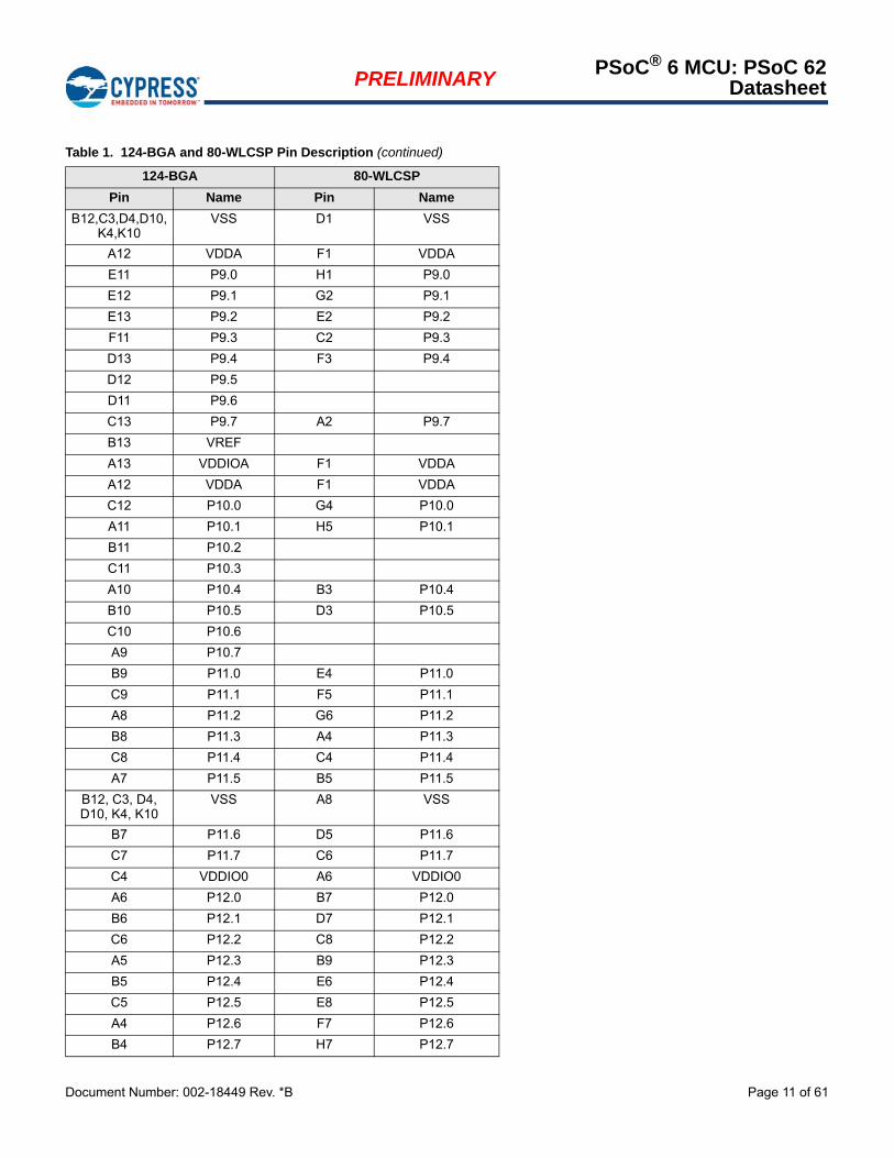
Document Number: 002-18449 Rev. *B Page 11 of 61
PRELIMINARYPSoC® 6 MCU: PSoC 62
Datasheet
B12,C3,D4,D10,K4,K10
VSS D1 VSS
A12 VDDA F1 VDDA
E11 P9.0 H1 P9.0
E12 P9.1 G2 P9.1
E13 P9.2 E2 P9.2
F11 P9.3 C2 P9.3
D13 P9.4 F3 P9.4
D12 P9.5
D11 P9.6
C13 P9.7 A2 P9.7
B13 VREF
A13 VDDIOA F1 VDDA
A12 VDDA F1 VDDA
C12 P10.0 G4 P10.0
A11 P10.1 H5 P10.1
B11 P10.2
C11 P10.3
A10 P10.4 B3 P10.4
B10 P10.5 D3 P10.5
C10 P10.6
A9 P10.7
B9 P11.0 E4 P11.0
C9 P11.1 F5 P11.1
A8 P11.2 G6 P11.2
B8 P11.3 A4 P11.3
C8 P11.4 C4 P11.4
A7 P11.5 B5 P11.5
B12, C3, D4, D10, K4, K10
VSS A8 VSS
B7 P11.6 D5 P11.6
C7 P11.7 C6 P11.7
C4 VDDIO0 A6 VDDIO0
A6 P12.0 B7 P12.0
B6 P12.1 D7 P12.1
C6 P12.2 C8 P12.2
A5 P12.3 B9 P12.3
B5 P12.4 E6 P12.4
C5 P12.5 E8 P12.5
A4 P12.6 F7 P12.6
B4 P12.7 H7 P12.7
Table 1. 124-BGA and 80-WLCSP Pin Description (continued)
124-BGA 80-WLCSP
Pin Name Pin Name
Document Number: 002-18449 Rev. *B Page 12 of 61
PRELIMINARYPSoC® 6 MCU: PSoC 62
Datasheet
The correspondence of power supplies to ports by package type is as follows:
P0: VBACKUP
P1: VDDD. Port 1 GPIO Pins are Overvoltage Tolerant (OVT).
P2, P3, P4: VDDIOR
P5, P6, P7, P8: VDDIO1
P9, P10: VDDIO, VDDA (VDDIO and VDDA must be connected together on the PCB)
P11, P12, P13: VDDIO0
P14: VDDUSB
B1 P13.0
A3 P13.1
B3 P13.2
B2 P13.3
C2 P13.4
C1 P13.5
D3 P13.6
D2 P13.7
Table 1. 124-BGA and 80-WLCSP Pin Description (continued)
124-BGA 80-WLCSP
Pin Name Pin Name
Document Number: 002-18449 Rev. *B Page 13 of 61
PRELIMINARY PSoC® 6 MCU: PSoC 62Datasheet
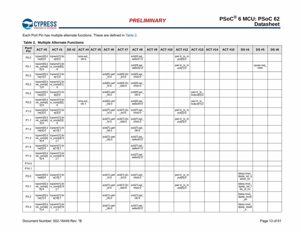
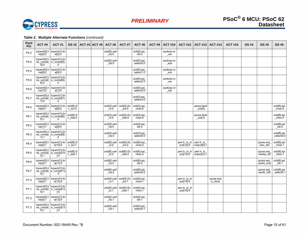
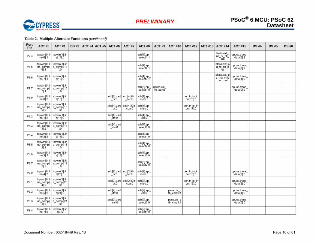
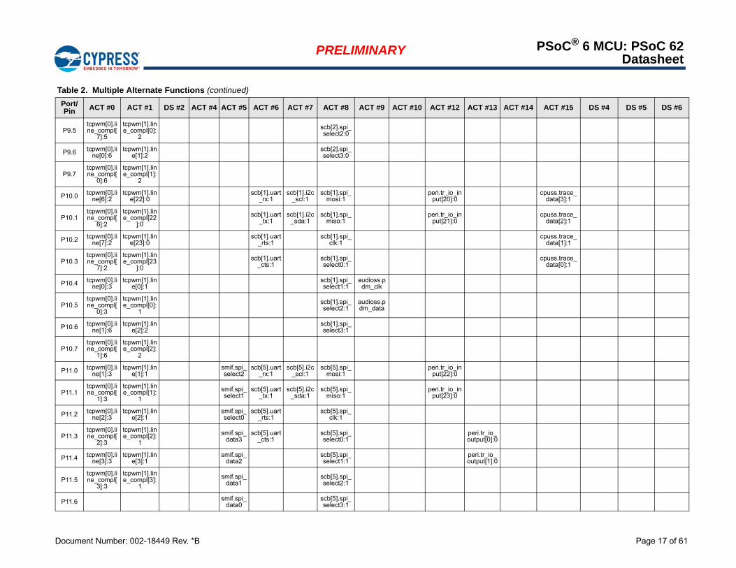
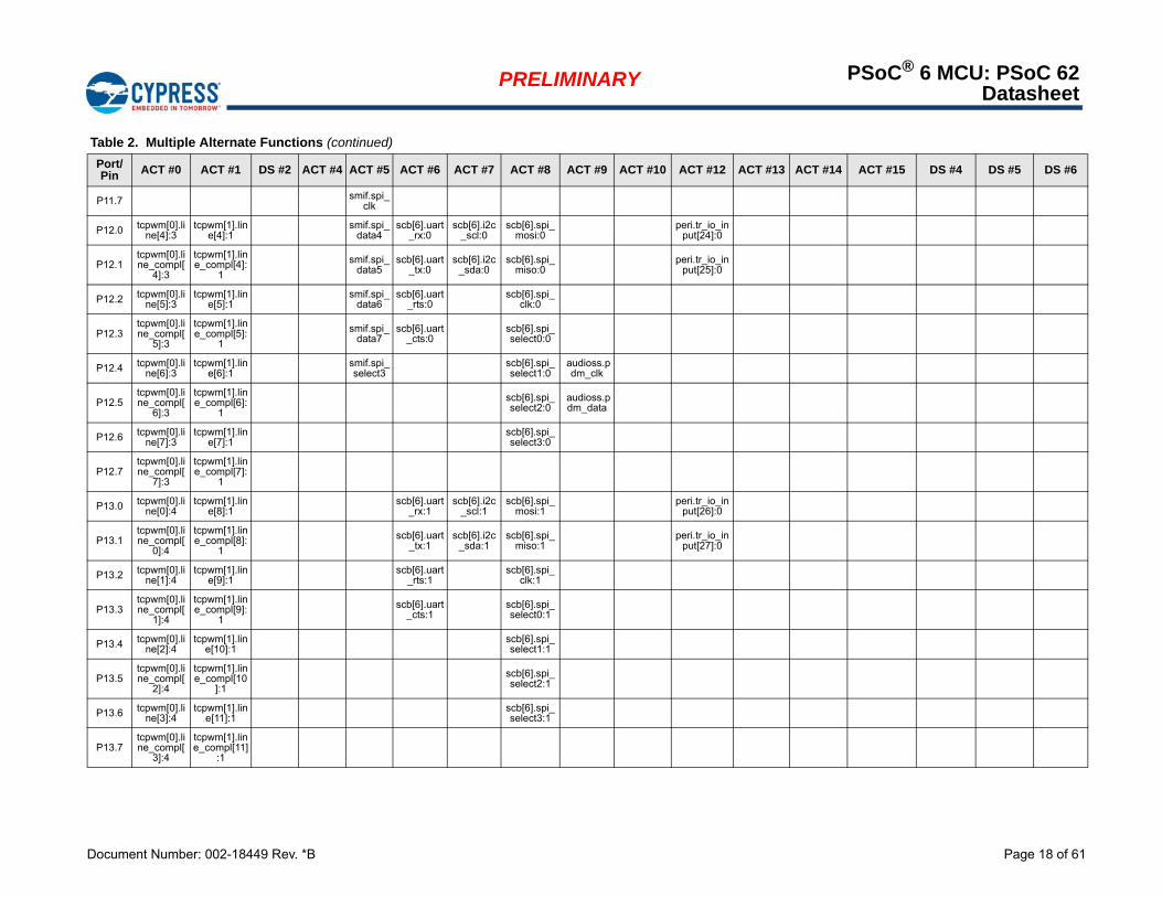
Each Port Pin has multiple alternate functions. These are defined in Table 2.
Table 2. Multiple Alternate Functions
Port/Pin ACT #0 ACT #1 DS #2 ACT #4 ACT #5 ACT #6 ACT #7 ACT #8 ACT #9 ACT #10 ACT #12 ACT #13 ACT #14 ACT #15 DS #4 DS #5 DS #6
P0.0 tcpwm[0].line[0]:0
tcpwm[1].line[0]:0
srss.ext_clk:0
scb[0].spi_select1:0
peri.tr_io_input[0]:0
P0.1tcpwm[0].line_compl[
0]:0
tcpwm[1].line_compl[0]:
0
scb[0].spi_select2:0
peri.tr_io_input[1]:0
cpuss.swj_trstn
P0.2 tcpwm[0].line[1]:0
tcpwm[1].line[1]:0
scb[0].uart_rx:0
scb[0].i2c_scl:0
scb[0].spi_mosi:0
P0.3tcpwm[0].line_compl[
1]:0
tcpwm[1].line_compl[1]:
0
scb[0].uart_tx:0
scb[0].i2c_sda:0
scb[0].spi_miso:0
P0.4 tcpwm[0].line[2]:0
tcpwm[1].line[2]:0
scb[0].uart_rts:0
scb[0].spi_clk:0
peri.tr_io_output[0]:2
P0.5tcpwm[0].line_compl[
2]:0
tcpwm[1].line_compl[2]:
0
srss.ext_clk:1
scb[0].uart_cts:0
scb[0].spi_select0:0
peri.tr_io_output[1]:2
P1.0 tcpwm[0].line[3]:0
tcpwm[1].line[3]:0
scb[7].uart_rx:0
scb[7].i2c_scl:0
scb[7].spi_mosi:0
peri.tr_io_input[2]:0
P1.1tcpwm[0].line_compl[
3]:0
tcpwm[1].line_compl[3]:
0
scb[7].uart_tx:0
scb[7].i2c_sda:0
scb[7].spi_miso:0
peri.tr_io_input[3]:0
P1.2 tcpwm[0].line[4]:4
tcpwm[1].line[12]:1
scb[7].uart_rts:0
scb[7].spi_clk:0
P1.3tcpwm[0].line_compl[
4]:4
tcpwm[1].line_compl[12
]:1
scb[7].uart_cts:0
scb[7].spi_select0:0
P1.4 tcpwm[0].line[5]:4
tcpwm[1].line[13]:1
scb[7].spi_select1:0
P1.5tcpwm[0].line_compl[
5]:4
tcpwm[1].line_compl[14
]:1
scb[7].spi_select2:0
P14.0
P14.1
P2.0 tcpwm[0].line[6]:4
tcpwm[1].line[15]:1
scb[1].uart_rx:0
scb[1].i2c_scl:0
scb[1].spi_mosi:0
peri.tr_io_input[4]:0
bless.mxd_dpslp_ret_s
witch_hv
P2.1tcpwm[0].line_compl[
6]:4
tcpwm[1].line_compl[15
]:1
scb[1].uart_tx:0
scb[1].i2c_sda:0
scb[1].spi_miso:0
peri.tr_io_input[5]:0
bless.mxd_dpslp_ret_ldo_ol_hv
P2.2 tcpwm[0].line[7]:4
tcpwm[1].line[16]:1
scb[1].uart_rts:0
scb[1].spi_clk:0
bless.mxd_dpslp_buck
_en
P2.3tcpwm[0].line_compl[
7]:4
tcpwm[1].line_compl[16
]:1
scb[1].uart_cts:0
scb[1].spi_select0:0
bless.mxd_dpslp_reset
_n
Document Number: 002-18449 Rev. *B Page 14 of 61
PRELIMINARY PSoC® 6 MCU: PSoC 62Datasheet
P2.4 tcpwm[0].line[0]:5
tcpwm[1].line[17]:1
scb[1].spi_select1:0
bless.mxd_dpslp_clk_
en
P2.5tcpwm[0].line_compl[
0]:5
tcpwm[1].line_compl[17
]:1
scb[1].spi_select2:0
bless.mxd_dpslp_isola
te_n
P2.6 tcpwm[0].line[1]:5
tcpwm[1].line[18]:1
scb[1].spi_select3:0
bless.mxd_dpslp_act_l
do_en
P2.7tcpwm[0].line_compl[
1]:5
tcpwm[1].line_compl[18
]:1
bless.mxd_dpslp_xtal_
en
P3.0 tcpwm[0].line[2]:5
tcpwm[1].line[19]:1
scb[2].uart_rx:1
scb[2].i2c_scl:1
scb[2].spi_mosi:1
peri.tr_io_input[6]:0
bless.mxd_dpslp_dig_l
do_en
P3.1tcpwm[0].line_compl[
2]:5
tcpwm[1].line_compl[19
]:1
scb[2].uart_tx:1
scb[2].i2c_sda:1
scb[2].spi_miso:1
peri.tr_io_input[7]:0
bless.mxd_act_dbus_r
x_en
P3.2 tcpwm[0].line[3]:5
tcpwm[1].line[20]:1
scb[2].uart_rts:1
scb[2].spi_clk:1
bless.mxd_act_dbus_t
x_en
P3.3tcpwm[0].line_compl[
3]:5
tcpwm[1].line_compl[20
]:1
scb[2].uart_cts:1
scb[2].spi_select0:1
bless.mxd_act_bpktctl
P3.4 tcpwm[0].line[4]:5
tcpwm[1].line[21]:1
scb[2].spi_select1:1
bless.mxd_act_txd_rx
d
P3.5tcpwm[0].line_compl[
4]:5
tcpwm[1].line_compl[21
]:1
scb[2].spi_select2:1
bless.mxd_dpslp_rcb_
data
P4.0 tcpwm[0].line[5]:5
tcpwm[1].line[22]:1
scb[7].uart_rx:1
scb[7].i2c_scl:1
scb[7].spi_mosi:1
peri.tr_io_input[8]:0
bless.mxd_dpslp_rcb_
clk
P4.1tcpwm[0].line_compl[
5]:5
tcpwm[1].line_compl[22
]:1
scb[7].uart_tx:1
scb[7].i2c_sda:1
scb[7].spi_miso:1
peri.tr_io_input[9]:0
bless.mxd_dpslp_rcb_
le
P4.2 tcpwm[0].line[6]:5
tcpwm[1].line[23]:1
scb[7].uart_rts:1
scb[7].spi_clk:1
P4.3tcpwm[0].line_compl[
6]:5
tcpwm[1].line_compl[23
]:1
scb[7].uart_cts:1
scb[7].spi_select0:1
bless.mxd_dpslp_mxd_clk_out
P5.0 tcpwm[0].line[4]:0
tcpwm[1].line[4]:0
scb[5].uart_rx:0
scb[5].i2c_scl:0
scb[5].spi_mosi:0
audioss.clk_i2s_if
peri.tr_io_input[10]:0
P5.1tcpwm[0].line_compl[
4]:0
tcpwm[1].line_compl[4]:
0
scb[5].uart_tx:0
scb[5].i2c_sda:0
scb[5].spi_miso:0
audioss.tx_sck
peri.tr_io_input[11]:0
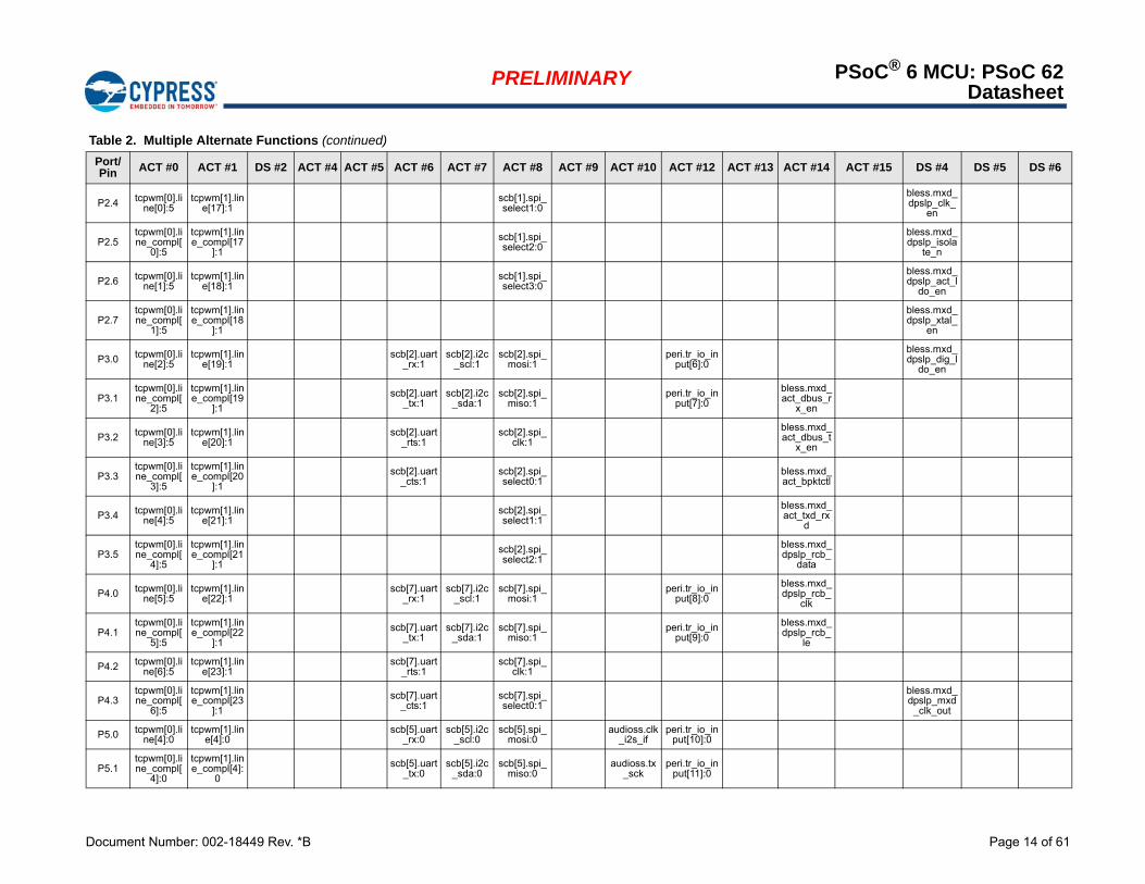
Table 2. Multiple Alternate Functions (continued)
Port/Pin ACT #0 ACT #1 DS #2 ACT #4 ACT #5 ACT #6 ACT #7 ACT #8 ACT #9 ACT #10 ACT #12 ACT #13 ACT #14 ACT #15 DS #4 DS #5 DS #6
Document Number: 002-18449 Rev. *B Page 15 of 61
PRELIMINARY PSoC® 6 MCU: PSoC 62Datasheet
P5.2 tcpwm[0].line[5]:0
tcpwm[1].line[5]:0
scb[5].uart_rts:0
scb[5].spi_clk:0
audioss.tx_ws
P5.3tcpwm[0].line_compl[
5]:0
tcpwm[1].line_compl[5]:
0
scb[5].uart_cts:0
scb[5].spi_select0:0
audioss.tx_sdo
P5.4 tcpwm[0].line[6]:0
tcpwm[1].line[6]:0
scb[5].spi_select1:0
audioss.rx_sck
P5.5tcpwm[0].line_compl[
6]:0
tcpwm[1].line_compl[6]:
0
scb[5].spi_select2:0
audioss.rx_ws
P5.6 tcpwm[0].line[7]:0
tcpwm[1].line[7]:0
scb[5].spi_select3:0
audioss.rx_sdi
P5.7tcpwm[0].line_compl[
7]:0
tcpwm[1].line_compl[7]:
0
scb[3].spi_select3:0
P6.0 tcpwm[0].line[0]:1
tcpwm[1].line[8]:0
scb[8].i2c_scl:0
scb[3].uart_rx:0
scb[3].i2c_scl:0
scb[3].spi_mosi:0
cpuss.fault_out[0]
scb[8].spi_mosi:0
P6.1tcpwm[0].line_compl[
0]:1
tcpwm[1].line_compl[8]:
0
scb[8].i2c_sda:0
scb[3].uart_tx:0
scb[3].i2c_sda:0
scb[3].spi_miso:0
cpuss.fault_out[1]
scb[8].spi_miso:0
P6.2 tcpwm[0].line[1]:1
tcpwm[1].line[9]:0
scb[3].uart_rts:0
scb[3].spi_clk:0
scb[8].spi_clk:0
P6.3tcpwm[0].line_compl[
1]:1
tcpwm[1].line_compl[9]:
0
scb[3].uart_cts:0
scb[3].spi_select0:0
scb[8].spi_select0:0
P6.4 tcpwm[0].line[2]:1
tcpwm[1].line[10]:0
scb[8].i2c_scl:1
scb[6].uart_rx:2
scb[6].i2c_scl:2
scb[6].spi_mosi:2
peri.tr_io_input[12]:0
peri.tr_io_output[0]:1
cpuss.swj_swo_tdo
scb[8].spi_mosi:1
P6.5tcpwm[0].line_compl[
2]:1
tcpwm[1].line_compl[10
]:0
scb[8].i2c_sda:1
scb[6].uart_tx:2
scb[6].i2c_sda:2
scb[6].spi_miso:2
peri.tr_io_input[13]:0
peri.tr_io_output[1]:1
cpuss.swj_swdoe_tdi
scb[8].spi_miso:1
P6.6 tcpwm[0].line[3]:1
tcpwm[1].line[11]:0
scb[6].uart_rts:2
scb[6].spi_clk:2
cpuss.swj_swdio_tms
scb[8].spi_clk:1
P6.7tcpwm[0].line_compl[
3]:1
tcpwm[1].line_compl[11]
:0
scb[6].uart_cts:2
scb[6].spi_select0:2
cpuss.swj_swclk_tclk
scb[8].spi_select0:1
P7.0 tcpwm[0].line[4]:1
tcpwm[1].line[12]:0
scb[4].uart_rx:1
scb[4].i2c_scl:1
scb[4].spi_mosi:1
peri.tr_io_input[14]:0
cpuss.trace_clock
P7.1tcpwm[0].line_compl[
4]:1
tcpwm[1].line_compl[12
]:0
scb[4].uart_tx:1
scb[4].i2c_sda:1
scb[4].spi_miso:1
peri.tr_io_input[15]:0
P7.2 tcpwm[0].line[5]:1
tcpwm[1].line[13]:0
scb[4].uart_rts:1
scb[4].spi_clk:1
P7.3tcpwm[0].line_compl[
5]:1
tcpwm[1].line_compl[13
]:0
scb[4].uart_cts:1
scb[4].spi_select0:1
Table 2. Multiple Alternate Functions (continued)
Port/Pin ACT #0 ACT #1 DS #2 ACT #4 ACT #5 ACT #6 ACT #7 ACT #8 ACT #9 ACT #10 ACT #12 ACT #13 ACT #14 ACT #15 DS #4 DS #5 DS #6
Document Number: 002-18449 Rev. *B Page 16 of 61
PRELIMINARY PSoC® 6 MCU: PSoC 62Datasheet
P7.4 tcpwm[0].line[6]:1
tcpwm[1].line[14]:0
scb[4].spi_select1:1
bless.ext_lna_rx_ctl_
out
cpuss.trace_data[3]:2
P7.5tcpwm[0].line_compl[
6]:1
tcpwm[1].line_compl[14
]:0
scb[4].spi_select2:1
bless.ext_pa_tx_ctl_o
ut
cpuss.trace_data[2]:2
P7.6 tcpwm[0].line[7]:1
tcpwm[1].line[15]:0
scb[4].spi_select3:1
bless.ext_pa_lna_chip
_en_out
cpuss.trace_data[1]:2
P7.7tcpwm[0].line_compl[
7]:1
tcpwm[1].line_compl[15
]:0
scb[3].spi_select1:0
cpuss.clk_fm_pump
cpuss.trace_data[0]:2
P8.0 tcpwm[0].line[0]:2
tcpwm[1].line[16]:0
scb[4].uart_rx:0
scb[4].i2c_scl:0
scb[4].spi_mosi:0
peri.tr_io_input[16]:0
P8.1tcpwm[0].line_compl[
0]:2
tcpwm[1].line_compl[16
]:0
scb[4].uart_tx:0
scb[4].i2c_sda:0
scb[4].spi_miso:0
peri.tr_io_input[17]:0
P8.2 tcpwm[0].line[1]:2
tcpwm[1].line[17]:0
scb[4].uart_rts:0
scb[4].spi_clk:0
P8.3tcpwm[0].line_compl[
1]:2
tcpwm[1].line_compl[17
]:0
scb[4].uart_cts:0
scb[4].spi_select0:0
P8.4 tcpwm[0].line[2]:2
tcpwm[1].line[18]:0
scb[4].spi_select1:0
P8.5tcpwm[0].line_compl[
2]:2
tcpwm[1].line_compl[18
]:0
scb[4].spi_select2:0
P8.6 tcpwm[0].line[3]:2
tcpwm[1].line[19]:0
scb[4].spi_select3:0
P8.7tcpwm[0].line_compl[
3]:2
tcpwm[1].line_compl[19
]:0
scb[3].spi_select2:0
P9.0 tcpwm[0].line[4]:2
tcpwm[1].line[20]:0
scb[2].uart_rx:0
scb[2].i2c_scl:0
scb[2].spi_mosi:0
peri.tr_io_input[18]:0
cpuss.trace_data[3]:0
P9.1tcpwm[0].line_compl[
4]:2
tcpwm[1].line_compl[20
]:0
scb[2].uart_tx:0
scb[2].i2c_sda:0
scb[2].spi_miso:0
peri.tr_io_input[19]:0
cpuss.trace_data[2]:0
P9.2 tcpwm[0].line[5]:2
tcpwm[1].line[21]:0
scb[2].uart_rts:0
scb[2].spi_clk:0
pass.dsi_ctb_cmp0:1
cpuss.trace_data[1]:0
P9.3tcpwm[0].line_compl[
5]:2
tcpwm[1].line_compl[21
]:0
scb[2].uart_cts:0
scb[2].spi_select0:0
pass.dsi_ctb_cmp1:1
cpuss.trace_data[0]:0
P9.4 tcpwm[0].line[7]:5
tcpwm[1].line[0]:2
scb[2].spi_select1:0
Table 2. Multiple Alternate Functions (continued)
Port/Pin ACT #0 ACT #1 DS #2 ACT #4 ACT #5 ACT #6 ACT #7 ACT #8 ACT #9 ACT #10 ACT #12 ACT #13 ACT #14 ACT #15 DS #4 DS #5 DS #6
Document Number: 002-18449 Rev. *B Page 17 of 61
PRELIMINARY PSoC® 6 MCU: PSoC 62Datasheet
P9.5tcpwm[0].line_compl[
7]:5
tcpwm[1].line_compl[0]:
2
scb[2].spi_select2:0
P9.6 tcpwm[0].line[0]:6
tcpwm[1].line[1]:2
scb[2].spi_select3:0
P9.7tcpwm[0].line_compl[
0]:6
tcpwm[1].line_compl[1]:
2
P10.0 tcpwm[0].line[6]:2
tcpwm[1].line[22]:0
scb[1].uart_rx:1
scb[1].i2c_scl:1
scb[1].spi_mosi:1
peri.tr_io_input[20]:0
cpuss.trace_data[3]:1
P10.1tcpwm[0].line_compl[
6]:2
tcpwm[1].line_compl[22
]:0
scb[1].uart_tx:1
scb[1].i2c_sda:1
scb[1].spi_miso:1
peri.tr_io_input[21]:0
cpuss.trace_data[2]:1
P10.2 tcpwm[0].line[7]:2
tcpwm[1].line[23]:0
scb[1].uart_rts:1
scb[1].spi_clk:1
cpuss.trace_data[1]:1
P10.3tcpwm[0].line_compl[
7]:2
tcpwm[1].line_compl[23
]:0
scb[1].uart_cts:1
scb[1].spi_select0:1
cpuss.trace_data[0]:1
P10.4 tcpwm[0].line[0]:3
tcpwm[1].line[0]:1
scb[1].spi_select1:1
audioss.pdm_clk
P10.5tcpwm[0].line_compl[
0]:3
tcpwm[1].line_compl[0]:
1
scb[1].spi_select2:1
audioss.pdm_data
P10.6 tcpwm[0].line[1]:6
tcpwm[1].line[2]:2
scb[1].spi_select3:1
P10.7tcpwm[0].line_compl[
1]:6
tcpwm[1].line_compl[2]:
2
P11.0 tcpwm[0].line[1]:3
tcpwm[1].line[1]:1
smif.spi_select2
scb[5].uart_rx:1
scb[5].i2c_scl:1
scb[5].spi_mosi:1
peri.tr_io_input[22]:0
P11.1tcpwm[0].line_compl[
1]:3
tcpwm[1].line_compl[1]:
1
smif.spi_select1
scb[5].uart_tx:1
scb[5].i2c_sda:1
scb[5].spi_miso:1
peri.tr_io_input[23]:0
P11.2 tcpwm[0].line[2]:3
tcpwm[1].line[2]:1
smif.spi_select0
scb[5].uart_rts:1
scb[5].spi_clk:1
P11.3tcpwm[0].line_compl[
2]:3
tcpwm[1].line_compl[2]:
1
smif.spi_data3
scb[5].uart_cts:1
scb[5].spi_select0:1
peri.tr_io_output[0]:0
P11.4 tcpwm[0].line[3]:3
tcpwm[1].line[3]:1
smif.spi_data2
scb[5].spi_select1:1
peri.tr_io_output[1]:0
P11.5tcpwm[0].line_compl[
3]:3
tcpwm[1].line_compl[3]:
1
smif.spi_data1
scb[5].spi_select2:1
P11.6 smif.spi_data0
scb[5].spi_select3:1
Table 2. Multiple Alternate Functions (continued)
Port/Pin ACT #0 ACT #1 DS #2 ACT #4 ACT #5 ACT #6 ACT #7 ACT #8 ACT #9 ACT #10 ACT #12 ACT #13 ACT #14 ACT #15 DS #4 DS #5 DS #6
Document Number: 002-18449 Rev. *B Page 18 of 61
PRELIMINARY PSoC® 6 MCU: PSoC 62Datasheet
P11.7 smif.spi_clk
P12.0 tcpwm[0].line[4]:3
tcpwm[1].line[4]:1
smif.spi_data4
scb[6].uart_rx:0
scb[6].i2c_scl:0
scb[6].spi_mosi:0
peri.tr_io_input[24]:0
P12.1tcpwm[0].line_compl[
4]:3
tcpwm[1].line_compl[4]:
1
smif.spi_data5
scb[6].uart_tx:0
scb[6].i2c_sda:0
scb[6].spi_miso:0
peri.tr_io_input[25]:0
P12.2 tcpwm[0].line[5]:3
tcpwm[1].line[5]:1
smif.spi_data6
scb[6].uart_rts:0
scb[6].spi_clk:0
P12.3tcpwm[0].line_compl[
5]:3
tcpwm[1].line_compl[5]:
1
smif.spi_data7
scb[6].uart_cts:0
scb[6].spi_select0:0
P12.4 tcpwm[0].line[6]:3
tcpwm[1].line[6]:1
smif.spi_select3
scb[6].spi_select1:0
audioss.pdm_clk
P12.5tcpwm[0].line_compl[
6]:3
tcpwm[1].line_compl[6]:
1
scb[6].spi_select2:0
audioss.pdm_data
P12.6 tcpwm[0].line[7]:3
tcpwm[1].line[7]:1
scb[6].spi_select3:0
P12.7tcpwm[0].line_compl[
7]:3
tcpwm[1].line_compl[7]:
1
P13.0 tcpwm[0].line[0]:4
tcpwm[1].line[8]:1
scb[6].uart_rx:1
scb[6].i2c_scl:1
scb[6].spi_mosi:1
peri.tr_io_input[26]:0
P13.1tcpwm[0].line_compl[
0]:4
tcpwm[1].line_compl[8]:
1
scb[6].uart_tx:1
scb[6].i2c_sda:1
scb[6].spi_miso:1
peri.tr_io_input[27]:0
P13.2 tcpwm[0].line[1]:4
tcpwm[1].line[9]:1
scb[6].uart_rts:1
scb[6].spi_clk:1
P13.3tcpwm[0].line_compl[
1]:4
tcpwm[1].line_compl[9]:
1
scb[6].uart_cts:1
scb[6].spi_select0:1
P13.4 tcpwm[0].line[2]:4
tcpwm[1].line[10]:1
scb[6].spi_select1:1
P13.5tcpwm[0].line_compl[
2]:4
tcpwm[1].line_compl[10
]:1
scb[6].spi_select2:1
P13.6 tcpwm[0].line[3]:4
tcpwm[1].line[11]:1
scb[6].spi_select3:1
P13.7tcpwm[0].line_compl[
3]:4
tcpwm[1].line_compl[11]
:1
Table 2. Multiple Alternate Functions (continued)
Port/Pin ACT #0 ACT #1 DS #2 ACT #4 ACT #5 ACT #6 ACT #7 ACT #8 ACT #9 ACT #10 ACT #12 ACT #13 ACT #14 ACT #15 DS #4 DS #5 DS #6
Document Number: 002-18449 Rev. *B Page 19 of 61
PRELIMINARYPSoC® 6 MCU: PSoC 62
Datasheet
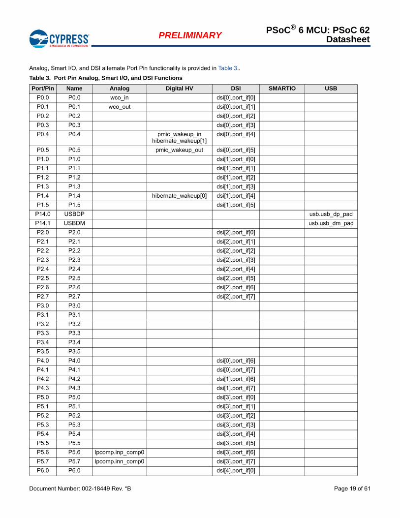
Analog, Smart I/O, and DSI alternate Port Pin functionality is provided in Table 3..
Table 3. Port Pin Analog, Smart I/O, and DSI Functions
Port/Pin Name Analog Digital HV DSI SMARTIO USB
P0.0 P0.0 wco_in dsi[0].port_if[0]
P0.1 P0.1 wco_out dsi[0].port_if[1]
P0.2 P0.2 dsi[0].port_if[2]
P0.3 P0.3 dsi[0].port_if[3]
P0.4 P0.4 pmic_wakeup_inhibernate_wakeup[1]
dsi[0].port_if[4]
P0.5 P0.5 pmic_wakeup_out dsi[0].port_if[5]
P1.0 P1.0 dsi[1].port_if[0]
P1.1 P1.1 dsi[1].port_if[1]
P1.2 P1.2 dsi[1].port_if[2]
P1.3 P1.3 dsi[1].port_if[3]
P1.4 P1.4 hibernate_wakeup[0] dsi[1].port_if[4]
P1.5 P1.5 dsi[1].port_if[5]
P14.0 USBDP usb.usb_dp_pad
P14.1 USBDM usb.usb_dm_pad
P2.0 P2.0 dsi[2].port_if[0]
P2.1 P2.1 dsi[2].port_if[1]
P2.2 P2.2 dsi[2].port_if[2]
P2.3 P2.3 dsi[2].port_if[3]
P2.4 P2.4 dsi[2].port_if[4]
P2.5 P2.5 dsi[2].port_if[5]
P2.6 P2.6 dsi[2].port_if[6]
P2.7 P2.7 dsi[2].port_if[7]
P3.0 P3.0
P3.1 P3.1
P3.2 P3.2
P3.3 P3.3
P3.4 P3.4
P3.5 P3.5
P4.0 P4.0 dsi[0].port_if[6]
P4.1 P4.1 dsi[0].port_if[7]
P4.2 P4.2 dsi[1].port_if[6]
P4.3 P4.3 dsi[1].port_if[7]
P5.0 P5.0 dsi[3].port_if[0]
P5.1 P5.1 dsi[3].port_if[1]
P5.2 P5.2 dsi[3].port_if[2]
P5.3 P5.3 dsi[3].port_if[3]
P5.4 P5.4 dsi[3].port_if[4]
P5.5 P5.5 dsi[3].port_if[5]
P5.6 P5.6 lpcomp.inp_comp0 dsi[3].port_if[6]
P5.7 P5.7 lpcomp.inn_comp0 dsi[3].port_if[7]
P6.0 P6.0 dsi[4].port_if[0]
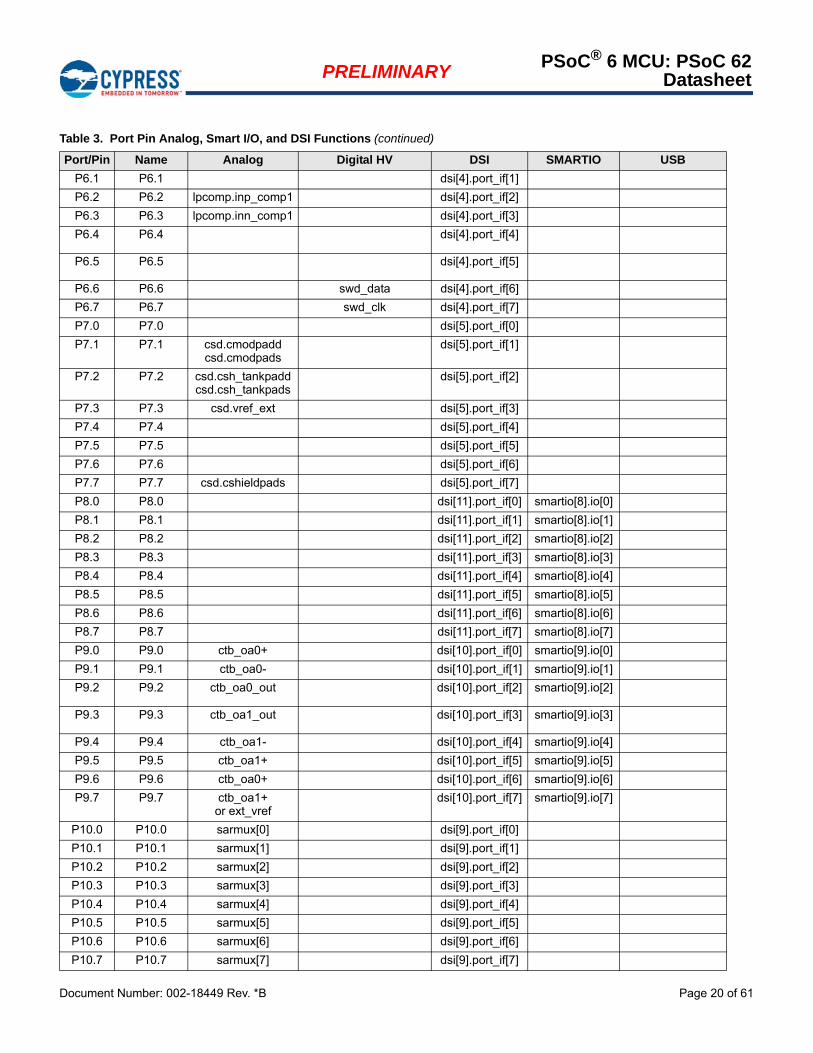
Document Number: 002-18449 Rev. *B Page 20 of 61
PRELIMINARYPSoC® 6 MCU: PSoC 62
Datasheet
P6.1 P6.1 dsi[4].port_if[1]
P6.2 P6.2 lpcomp.inp_comp1 dsi[4].port_if[2]
P6.3 P6.3 lpcomp.inn_comp1 dsi[4].port_if[3]
P6.4 P6.4 dsi[4].port_if[4]
P6.5 P6.5 dsi[4].port_if[5]
P6.6 P6.6 swd_data dsi[4].port_if[6]
P6.7 P6.7 swd_clk dsi[4].port_if[7]
P7.0 P7.0 dsi[5].port_if[0]
P7.1 P7.1 csd.cmodpaddcsd.cmodpads
dsi[5].port_if[1]
P7.2 P7.2 csd.csh_tankpaddcsd.csh_tankpads
dsi[5].port_if[2]
P7.3 P7.3 csd.vref_ext dsi[5].port_if[3]
P7.4 P7.4 dsi[5].port_if[4]
P7.5 P7.5 dsi[5].port_if[5]
P7.6 P7.6 dsi[5].port_if[6]
P7.7 P7.7 csd.cshieldpads dsi[5].port_if[7]
P8.0 P8.0 dsi[11].port_if[0] smartio[8].io[0]
P8.1 P8.1 dsi[11].port_if[1] smartio[8].io[1]
P8.2 P8.2 dsi[11].port_if[2] smartio[8].io[2]
P8.3 P8.3 dsi[11].port_if[3] smartio[8].io[3]
P8.4 P8.4 dsi[11].port_if[4] smartio[8].io[4]
P8.5 P8.5 dsi[11].port_if[5] smartio[8].io[5]
P8.6 P8.6 dsi[11].port_if[6] smartio[8].io[6]
P8.7 P8.7 dsi[11].port_if[7] smartio[8].io[7]
P9.0 P9.0 ctb_oa0+ dsi[10].port_if[0] smartio[9].io[0]
P9.1 P9.1 ctb_oa0- dsi[10].port_if[1] smartio[9].io[1]
P9.2 P9.2 ctb_oa0_out dsi[10].port_if[2] smartio[9].io[2]
P9.3 P9.3 ctb_oa1_out dsi[10].port_if[3] smartio[9].io[3]
P9.4 P9.4 ctb_oa1- dsi[10].port_if[4] smartio[9].io[4]
P9.5 P9.5 ctb_oa1+ dsi[10].port_if[5] smartio[9].io[5]
P9.6 P9.6 ctb_oa0+ dsi[10].port_if[6] smartio[9].io[6]
P9.7 P9.7 ctb_oa1+ or ext_vref
dsi[10].port_if[7] smartio[9].io[7]
P10.0 P10.0 sarmux[0] dsi[9].port_if[0]
P10.1 P10.1 sarmux[1] dsi[9].port_if[1]
P10.2 P10.2 sarmux[2] dsi[9].port_if[2]
P10.3 P10.3 sarmux[3] dsi[9].port_if[3]
P10.4 P10.4 sarmux[4] dsi[9].port_if[4]
P10.5 P10.5 sarmux[5] dsi[9].port_if[5]
P10.6 P10.6 sarmux[6] dsi[9].port_if[6]
P10.7 P10.7 sarmux[7] dsi[9].port_if[7]
Table 3. Port Pin Analog, Smart I/O, and DSI Functions (continued)
Port/Pin Name Analog Digital HV DSI SMARTIO USB
Document Number: 002-18449 Rev. *B Page 21 of 61
PRELIMINARYPSoC® 6 MCU: PSoC 62
Datasheet
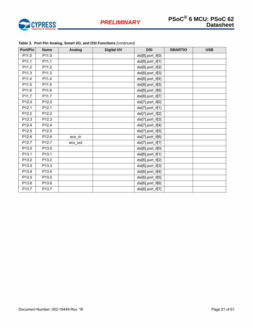
P11.0 P11.0 dsi[8].port_if[0]
P11.1 P11.1 dsi[8].port_if[1]
P11.2 P11.2 dsi[8].port_if[2]
P11.3 P11.3 dsi[8].port_if[3]
P11.4 P11.4 dsi[8].port_if[4]
P11.5 P11.5 dsi[8].port_if[5]
P11.6 P11.6 dsi[8].port_if[6]
P11.7 P11.7 dsi[8].port_if[7]
P12.0 P12.0 dsi[7].port_if[0]
P12.1 P12.1 dsi[7].port_if[1]
P12.2 P12.2 dsi[7].port_if[2]
P12.3 P12.3 dsi[7].port_if[3]
P12.4 P12.4 dsi[7].port_if[4]
P12.5 P12.5 dsi[7].port_if[5]
P12.6 P12.6 eco_in dsi[7].port_if[6]
P12.7 P12.7 eco_out dsi[7].port_if[7]
P13.0 P13.0 dsi[6].port_if[0]
P13.1 P13.1 dsi[6].port_if[1]
P13.2 P13.2 dsi[6].port_if[2]
P13.3 P13.3 dsi[6].port_if[3]
P13.4 P13.4 dsi[6].port_if[4]
P13.5 P13.5 dsi[6].port_if[5]
P13.6 P13.6 dsi[6].port_if[6]
P13.7 P13.7 dsi[6].port_if[7]
Table 3. Port Pin Analog, Smart I/O, and DSI Functions (continued)
Port/Pin Name Analog Digital HV DSI SMARTIO USB
Document Number: 002-18449 Rev. *B Page 22 of 61
PRELIMINARYPSoC® 6 MCU: PSoC 62
Datasheet
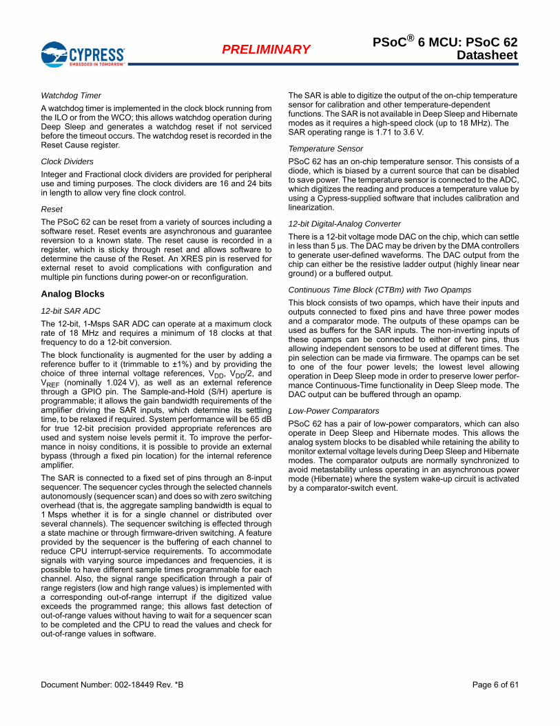
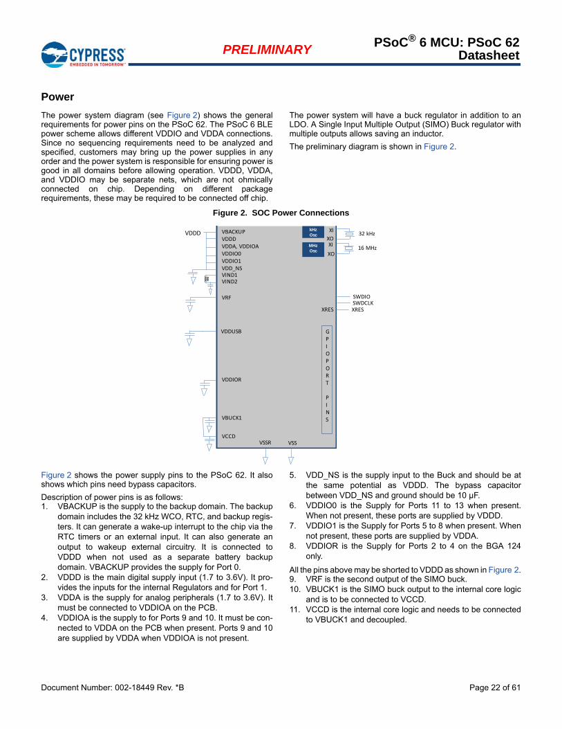
Power
The power system diagram (see Figure 2) shows the generalrequirements for power pins on the PSoC 62. The PSoC 6 BLEpower scheme allows different VDDIO and VDDA connections.Since no sequencing requirements need to be analyzed andspecified, customers may bring up the power supplies in anyorder and the power system is responsible for ensuring power isgood in all domains before allowing operation. VDDD, VDDA,and VDDIO may be separate nets, which are not ohmicallyconnected on chip. Depending on different packagerequirements, these may be required to be connected off chip.
The power system will have a buck regulator in addition to anLDO. A Single Input Multiple Output (SIMO) Buck regulator withmultiple outputs allows saving an inductor.
The preliminary diagram is shown in Figure 2.
Figure 2. SOC Power Connections
Figure 2 shows the power supply pins to the PSoC 62. It alsoshows which pins need bypass capacitors.
Description of power pins is as follows:1. VBACKUP is the supply to the backup domain. The backup
domain includes the 32 kHz WCO, RTC, and backup regis-ters. It can generate a wake-up interrupt to the chip via theRTC timers or an external input. It can also generate anoutput to wakeup external circuitry. It is connected toVDDD when not used as a separate battery backupdomain. VBACKUP provides the supply for Port 0.
2. VDDD is the main digital supply input (1.7 to 3.6V). It pro-vides the inputs for the internal Regulators and for Port 1.
3. VDDA is the supply for analog peripherals (1.7 to 3.6V). Itmust be connected to VDDIOA on the PCB.
4. VDDIOA is the supply to for Ports 9 and 10. It must be con-nected to VDDA on the PCB when present. Ports 9 and 10are supplied by VDDA when VDDIOA is not present.
5. VDD_NS is the supply input to the Buck and should be atthe same potential as VDDD. The bypass capacitorbetween VDD_NS and ground should be 10 µF.
6. VDDIO0 is the Supply for Ports 11 to 13 when present.When not present, these ports are supplied by VDDD.
7. VDDIO1 is the Supply for Ports 5 to 8 when present. Whennot present, these ports are supplied by VDDA.
8. VDDIOR is the Supply for Ports 2 to 4 on the BGA 124only.
All the pins above may be shorted to VDDD as shown in Figure 2.9. VRF is the second output of the SIMO buck.10. VBUCK1 is the SIMO buck output to the internal core logic
and is to be connected to VCCD.11. VCCD is the internal core logic and needs to be connected
to VBUCK1 and decoupled.
VBACKUPVDDDVDDA, VDDIOAVDDIO0VDDIO1VDD_NS
VDDD
VCCD
VIND1VIND2
VSS
VRF
VDDIOR
XO32 kHz
XI
SWDIOSWDCLK
XRES XRES
kHzOsc
VBUCK1
VSSR
16 MHzXI
XO
MHz Osc
GPIOPORT
PINS
VDDUSB
Document Number: 002-18449 Rev. *B Page 23 of 61
PRELIMINARYPSoC® 6 MCU: PSoC 62
Datasheet
The supply voltage range is 1.71 to 3.6 V with all functions andcircuits operating over that range. All grounds must be shortedtogether on the PCB. Bypass capacitors must be used fromVDDD and VDDA to ground and wherever indicated in thediagram. Typical practice for systems in this frequency range isto use a capacitor in the 10-µF range in parallel with a smallercapacitor (0.1 µF, for example). Note that these are simply rulesof thumb and that, for critical applications, the PCB layout, lead
inductance, and the bypass capacitor parasitic should besimulated to design and obtain optimal bypassing. Recom-mended Buck output capacitor values are 10 µF for Vrf and4.7 µF for Vbuck2. The capacitor connected to Vind2 should be100 nF.
Document Number: 002-18449 Rev. *B Page 24 of 61
PRELIMINARYPSoC® 6 MCU: PSoC 62
Datasheet
Development Support
The PSoC 62 family has a rich set of documentation, development tools, and online resources to assist you during your developmentprocess. Visit www.cypress.com/products/32-bit-arm-cortex-m0-psoc-4 to find out more.
Documentation
A suite of documentation supports the PSoC 62 family to ensurethat you can find answers to your questions quickly. This sectioncontains a list of some of the key documents.
Software User Guide: A step-by-step guide for using PSoCCreator. The software user guide shows you how the PSoCCreator build process works in detail, how to use source controlwith PSoC Creator, and much more.
Component Datasheets: The flexibility of PSoC allows thecreation of new peripherals (Components) long after the devicehas gone into production. Component datasheets provide all ofthe information needed to select and use a particularComponent, including a functional description, API documen-tation, example code, and AC/DC specifications.
Technical Reference Manual: The Technical Reference Manual(TRM) contains all the technical detail you need to use a PSoCdevice, including a complete description of all PSoC registers.The TRM is available in the Documentation section atwww.cypress.com/products/32-bit-arm-cortex-m0-psoc-4.
Online
In addition to print documentation, the Cypress PSoC forumsconnect you with fellow PSoC users and experts in PSoC fromaround the world, 24 hours a day, 7 days a week.
Tools
With industry standard cores, programming, and debugginginterfaces, the PSoC 62 family is part of a development toolecosystem. Visit us atwww.cypress.com/products/psoc-creator-integrated-design-environment-ide for the latest information on the revolutionary, easyto use PSoC Creator IDE, supported third party compilers,programmers, debuggers, and development kits.
Document Number: 002-18449 Rev. *B Page 25 of 61
PRELIMINARYPSoC® 6 MCU: PSoC 62
Datasheet
Electrical Specifications
Note: These are preliminary and subject to change.
Absolute Maximum Ratings
Device-Level Specifications
All specifications are valid for –40 °C TA 85 °C and for 1.71 V to 3.6 V except where noted.
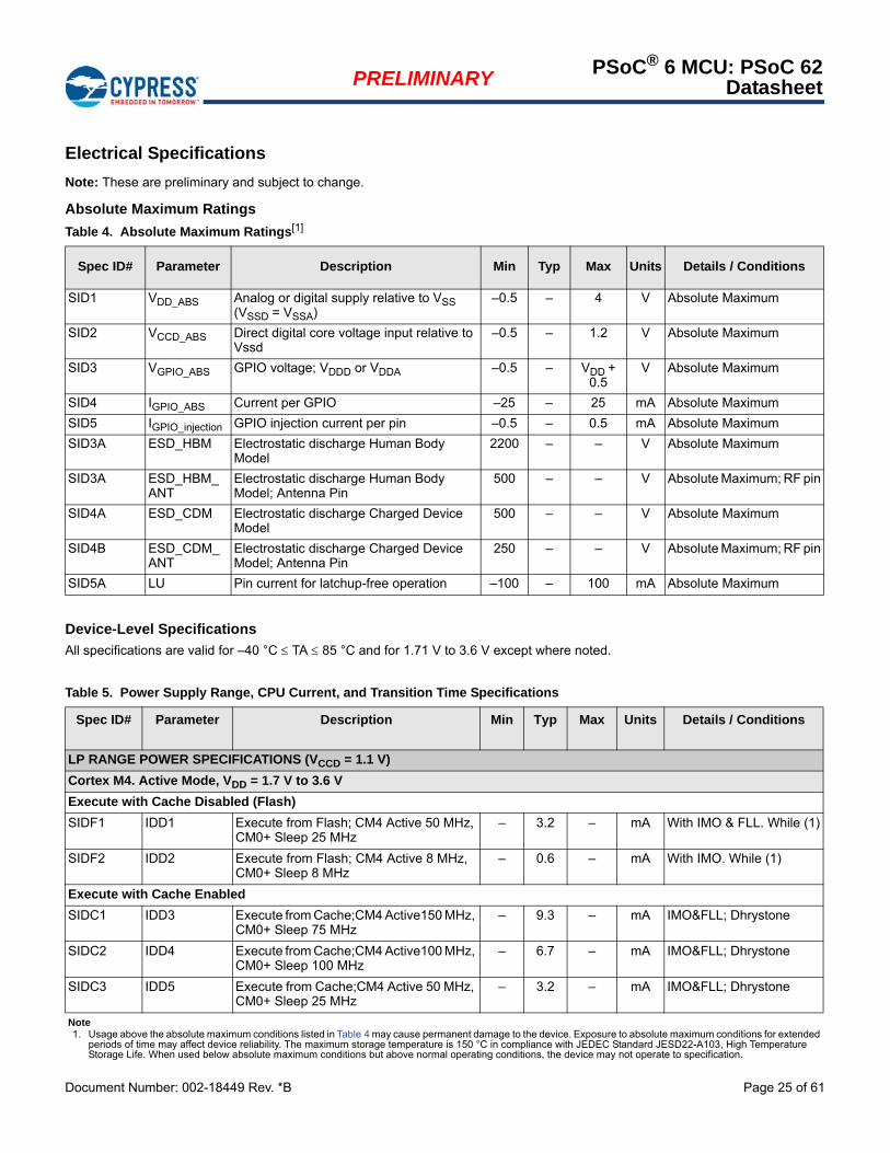
Table 4. Absolute Maximum Ratings[1]
Spec ID# Parameter Description Min Typ Max Units Details / Conditions
SID1 VDD_ABS Analog or digital supply relative to VSS (VSSD = VSSA)
–0.5 – 4 V Absolute Maximum
SID2 VCCD_ABS Direct digital core voltage input relative to Vssd
–0.5 – 1.2 V Absolute Maximum
SID3 VGPIO_ABS GPIO voltage; VDDD or VDDA –0.5 – VDD + 0.5
V Absolute Maximum
SID4 IGPIO_ABS Current per GPIO –25 – 25 mA Absolute Maximum
SID5 IGPIO_injection GPIO injection current per pin –0.5 – 0.5 mA Absolute Maximum
SID3A ESD_HBM Electrostatic discharge Human Body Model
2200 – – V Absolute Maximum
SID3A ESD_HBM_ANT
Electrostatic discharge Human Body Model; Antenna Pin
500 – – V Absolute Maximum; RF pin
SID4A ESD_CDM Electrostatic discharge Charged Device Model
500 – – V Absolute Maximum
SID4B ESD_CDM_ANT
Electrostatic discharge Charged Device Model; Antenna Pin
250 – – V Absolute Maximum; RF pin
SID5A LU Pin current for latchup-free operation –100 – 100 mA Absolute Maximum
Note1. Usage above the absolute maximum conditions listed in Table 4 may cause permanent damage to the device. Exposure to absolute maximum conditions for extended
periods of time may affect device reliability. The maximum storage temperature is 150 °C in compliance with JEDEC Standard JESD22-A103, High Temperature Storage Life. When used below absolute maximum conditions but above normal operating conditions, the device may not operate to specification.
Table 5. Power Supply Range, CPU Current, and Transition Time Specifications
Spec ID# Parameter Description Min Typ Max Units Details / Conditions
LP RANGE POWER SPECIFICATIONS (VCCD = 1.1 V)
Cortex M4. Active Mode, VDD = 1.7 V to 3.6 V
Execute with Cache Disabled (Flash)
SIDF1 IDD1 Execute from Flash; CM4 Active 50 MHz, CM0+ Sleep 25 MHz
– 3.2 – mA With IMO & FLL. While (1)
SIDF2 IDD2 Execute from Flash; CM4 Active 8 MHz, CM0+ Sleep 8 MHz
– 0.6 – mA With IMO. While (1)
Execute with Cache Enabled
SIDC1 IDD3 Execute from Cache;CM4 Active150 MHz, CM0+ Sleep 75 MHz
– 9.3 – mA IMO&FLL; Dhrystone
SIDC2 IDD4 Execute from Cache;CM4 Active100 MHz, CM0+ Sleep 100 MHz
– 6.7 – mA IMO&FLL; Dhrystone
SIDC3 IDD5 Execute from Cache;CM4 Active 50 MHz, CM0+ Sleep 25 MHz
– 3.2 – mA IMO&FLL; Dhrystone
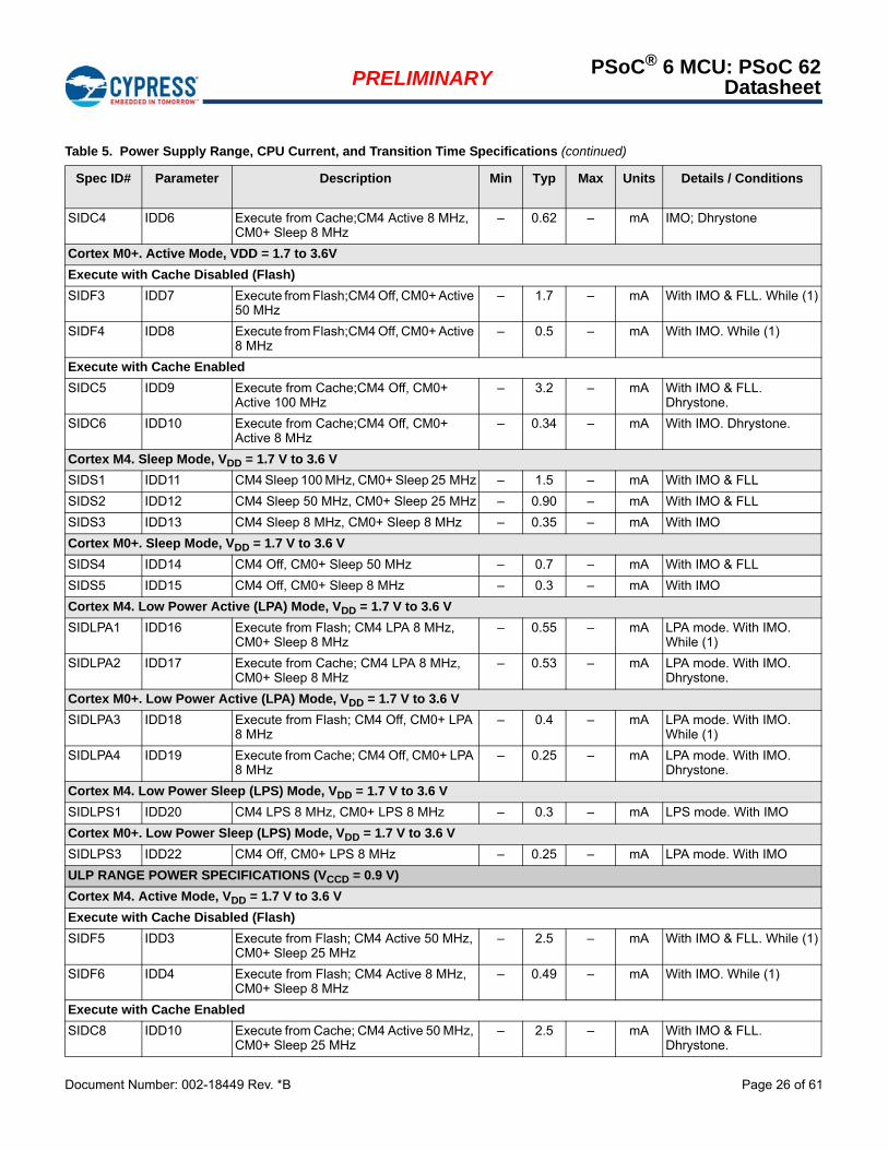
Document Number: 002-18449 Rev. *B Page 26 of 61
PRELIMINARYPSoC® 6 MCU: PSoC 62
Datasheet
SIDC4 IDD6 Execute from Cache;CM4 Active 8 MHz, CM0+ Sleep 8 MHz
– 0.62 – mA IMO; Dhrystone
Cortex M0+. Active Mode, VDD = 1.7 to 3.6V
Execute with Cache Disabled (Flash)
SIDF3 IDD7 Execute from Flash;CM4 Off, CM0+ Active 50 MHz
– 1.7 – mA With IMO & FLL. While (1)
SIDF4 IDD8 Execute from Flash;CM4 Off, CM0+ Active 8 MHz
– 0.5 – mA With IMO. While (1)
Execute with Cache Enabled
SIDC5 IDD9 Execute from Cache;CM4 Off, CM0+ Active 100 MHz
– 3.2 – mA With IMO & FLL. Dhrystone.
SIDC6 IDD10 Execute from Cache;CM4 Off, CM0+ Active 8 MHz
– 0.34 – mA With IMO. Dhrystone.
Cortex M4. Sleep Mode, VDD = 1.7 V to 3.6 V
SIDS1 IDD11 CM4 Sleep 100 MHz, CM0+ Sleep 25 MHz – 1.5 – mA With IMO & FLL
SIDS2 IDD12 CM4 Sleep 50 MHz, CM0+ Sleep 25 MHz – 0.90 – mA With IMO & FLL
SIDS3 IDD13 CM4 Sleep 8 MHz, CM0+ Sleep 8 MHz – 0.35 – mA With IMO
Cortex M0+. Sleep Mode, VDD = 1.7 V to 3.6 V
SIDS4 IDD14 CM4 Off, CM0+ Sleep 50 MHz – 0.7 – mA With IMO & FLL
SIDS5 IDD15 CM4 Off, CM0+ Sleep 8 MHz – 0.3 – mA With IMO
Cortex M4. Low Power Active (LPA) Mode, VDD = 1.7 V to 3.6 V
SIDLPA1 IDD16 Execute from Flash; CM4 LPA 8 MHz, CM0+ Sleep 8 MHz
– 0.55 – mA LPA mode. With IMO. While (1)
SIDLPA2 IDD17 Execute from Cache; CM4 LPA 8 MHz, CM0+ Sleep 8 MHz
– 0.53 – mA LPA mode. With IMO. Dhrystone.
Cortex M0+. Low Power Active (LPA) Mode, VDD = 1.7 V to 3.6 V
SIDLPA3 IDD18 Execute from Flash; CM4 Off, CM0+ LPA 8 MHz
– 0.4 – mA LPA mode. With IMO. While (1)
SIDLPA4 IDD19 Execute from Cache; CM4 Off, CM0+ LPA 8 MHz
– 0.25 – mA LPA mode. With IMO. Dhrystone.
Cortex M4. Low Power Sleep (LPS) Mode, VDD = 1.7 V to 3.6 V
SIDLPS1 IDD20 CM4 LPS 8 MHz, CM0+ LPS 8 MHz – 0.3 – mA LPS mode. With IMO
Cortex M0+. Low Power Sleep (LPS) Mode, VDD = 1.7 V to 3.6 V
SIDLPS3 IDD22 CM4 Off, CM0+ LPS 8 MHz – 0.25 – mA LPA mode. With IMO
ULP RANGE POWER SPECIFICATIONS (VCCD = 0.9 V)
Cortex M4. Active Mode, VDD = 1.7 V to 3.6 V
Execute with Cache Disabled (Flash)
SIDF5 IDD3 Execute from Flash; CM4 Active 50 MHz, CM0+ Sleep 25 MHz
– 2.5 – mA With IMO & FLL. While (1)
SIDF6 IDD4 Execute from Flash; CM4 Active 8 MHz, CM0+ Sleep 8 MHz
– 0.49 – mA With IMO. While (1)
Execute with Cache Enabled
SIDC8 IDD10 Execute from Cache; CM4 Active 50 MHz, CM0+ Sleep 25 MHz
– 2.5 – mA With IMO & FLL. Dhrystone.
Table 5. Power Supply Range, CPU Current, and Transition Time Specifications (continued)
Spec ID# Parameter Description Min Typ Max Units Details / Conditions
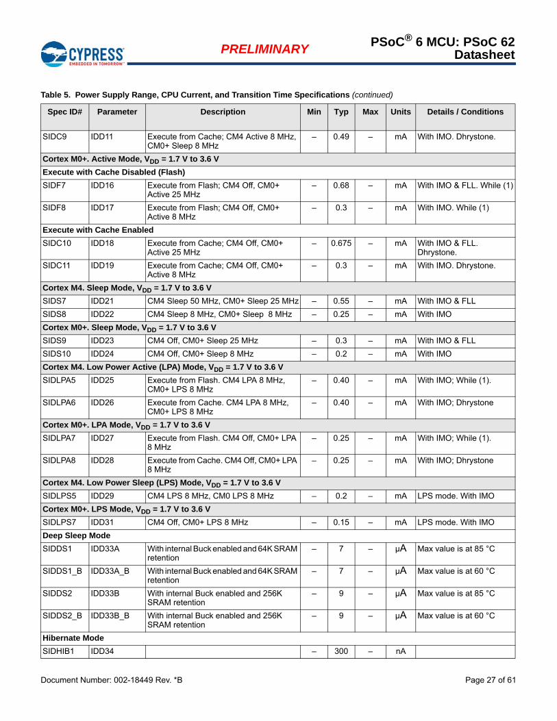
Document Number: 002-18449 Rev. *B Page 27 of 61
PRELIMINARYPSoC® 6 MCU: PSoC 62
Datasheet
SIDC9 IDD11 Execute from Cache; CM4 Active 8 MHz, CM0+ Sleep 8 MHz
– 0.49 – mA With IMO. Dhrystone.
Cortex M0+. Active Mode, VDD = 1.7 V to 3.6 V
Execute with Cache Disabled (Flash)
SIDF7 IDD16 Execute from Flash; CM4 Off, CM0+ Active 25 MHz
– 0.68 – mA With IMO & FLL. While (1)
SIDF8 IDD17 Execute from Flash; CM4 Off, CM0+ Active 8 MHz
– 0.3 – mA With IMO. While (1)
Execute with Cache Enabled
SIDC10 IDD18 Execute from Cache; CM4 Off, CM0+ Active 25 MHz
– 0.675 – mA With IMO & FLL. Dhrystone.
SIDC11 IDD19 Execute from Cache; CM4 Off, CM0+ Active 8 MHz
– 0.3 – mA With IMO. Dhrystone.
Cortex M4. Sleep Mode, VDD = 1.7 V to 3.6 V
SIDS7 IDD21 CM4 Sleep 50 MHz, CM0+ Sleep 25 MHz – 0.55 – mA With IMO & FLL
SIDS8 IDD22 CM4 Sleep 8 MHz, CM0+ Sleep 8 MHz – 0.25 – mA With IMO
Cortex M0+. Sleep Mode, VDD = 1.7 V to 3.6 V
SIDS9 IDD23 CM4 Off, CM0+ Sleep 25 MHz – 0.3 – mA With IMO & FLL
SIDS10 IDD24 CM4 Off, CM0+ Sleep 8 MHz – 0.2 – mA With IMO
Cortex M4. Low Power Active (LPA) Mode, VDD = 1.7 V to 3.6 V
SIDLPA5 IDD25 Execute from Flash. CM4 LPA 8 MHz, CM0+ LPS 8 MHz
– 0.40 – mA With IMO; While (1).
SIDLPA6 IDD26 Execute from Cache. CM4 LPA 8 MHz, CM0+ LPS 8 MHz
– 0.40 – mA With IMO; Dhrystone
Cortex M0+. LPA Mode, VDD = 1.7 V to 3.6 V
SIDLPA7 IDD27 Execute from Flash. CM4 Off, CM0+ LPA 8 MHz
– 0.25 – mA With IMO; While (1).
SIDLPA8 IDD28 Execute from Cache. CM4 Off, CM0+ LPA 8 MHz
– 0.25 – mA With IMO; Dhrystone
Cortex M4. Low Power Sleep (LPS) Mode, VDD = 1.7 V to 3.6 V
SIDLPS5 IDD29 CM4 LPS 8 MHz, CM0 LPS 8 MHz – 0.2 – mA LPS mode. With IMO
Cortex M0+. LPS Mode, VDD = 1.7 V to 3.6 V
SIDLPS7 IDD31 CM4 Off, CM0+ LPS 8 MHz – 0.15 – mA LPS mode. With IMO
Deep Sleep Mode
SIDDS1 IDD33A With internal Buck enabled and 64K SRAM retention
– 7 – µA Max value is at 85 °C
SIDDS1_B IDD33A_B With internal Buck enabled and 64K SRAM retention
– 7 – µA Max value is at 60 °C
SIDDS2 IDD33B With internal Buck enabled and 256K SRAM retention
– 9 – µA Max value is at 85 °C
SIDDS2_B IDD33B_B With internal Buck enabled and 256K SRAM retention
– 9 – µA Max value is at 60 °C
Hibernate Mode
SIDHIB1 IDD34 – 300 – nA
Table 5. Power Supply Range, CPU Current, and Transition Time Specifications (continued)
Spec ID# Parameter Description Min Typ Max Units Details / Conditions
Document Number: 002-18449 Rev. *B Page 28 of 61
PRELIMINARYPSoC® 6 MCU: PSoC 62
Datasheet
XRES
GPIO
Power Mode Transition Times
SID12 TLPACT_ACT Low Power Active to Active transition time – 100 – µs Including PLL lock time
SID13 TDS_LPACT Deep Sleep to LP Active transition time – – 21 µs Transition to Firmware execution
SID13A TDS_ACT Deep Sleep to Active transition time – – 21 µs Transition to Firmware execution
SID14 THIB_ACT Hibernate to Active transition time – 500 – µs Including PLL lock time
Table 5. Power Supply Range, CPU Current, and Transition Time Specifications (continued)
Spec ID# Parameter Description Min Typ Max Units Details / Conditions
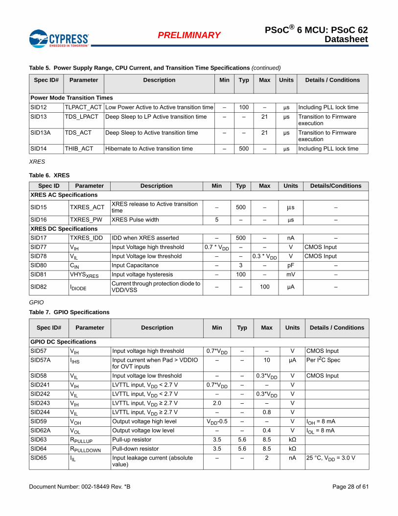
Table 6. XRES
Spec ID Parameter Description Min Typ Max Units Details/Conditions
XRES AC Specifications
SID15 TXRES_ACT XRES release to Active transition time – 500 – s –
SID16 TXRES_PW XRES Pulse width 5 – – µs –
XRES DC Specifications
SID17 TXRES_IDD IDD when XRES asserted – 500 – nA –
SID77 VIH Input Voltage high threshold 0.7 * VDD – – V CMOS Input
SID78 VIL Input Voltage low threshold – – 0.3 * VDD V CMOS Input
SID80 CIN Input Capacitance – 3 – pF –
SID81 VHYSXRES Input voltage hysteresis – 100 – mV –
SID82 IDIODECurrent through protection diode to VDD/VSS
– – 100 µA –
Table 7. GPIO Specifications
Spec ID# Parameter Description Min Typ Max Units Details / Conditions
GPIO DC Specifications
SID57 VIH Input voltage high threshold 0.7*VDD – – V CMOS Input
SID57A IIHS Input current when Pad > VDDIO for OVT inputs
– – 10 µA Per I2C Spec
SID58 VIL Input voltage low threshold – – 0.3*VDD V CMOS Input
SID241 VIH LVTTL input, VDD < 2.7 V 0.7*VDD – – V
SID242 VIL LVTTL input, VDD < 2.7 V – – 0.3*VDD V
SID243 VIH LVTTL input, VDD ≥ 2.7 V 2.0 – – V
SID244 VIL LVTTL input, VDD ≥ 2.7 V – – 0.8 V
SID59 VOH Output voltage high level VDD-0.5 – – V IOH = 8 mA
SID62A VOL Output voltage low level – – 0.4 V IOL = 8 mA
SID63 RPULLUP Pull-up resistor 3.5 5.6 8.5 kΩ
SID64 RPULLDOWN Pull-down resistor 3.5 5.6 8.5 kΩ
SID65 IIL Input leakage current (absolute value)
– – 2 nA 25 °C, VDD = 3.0 V
Document Number: 002-18449 Rev. *B Page 29 of 61
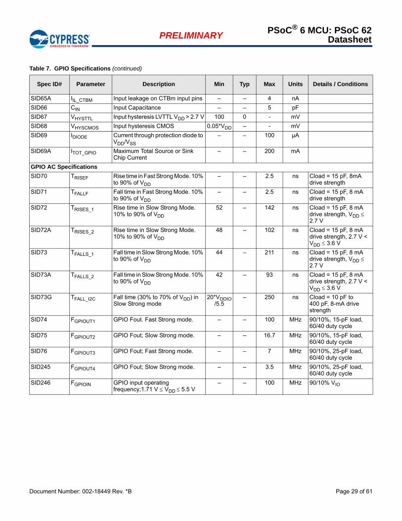
PRELIMINARYPSoC® 6 MCU: PSoC 62
Datasheet
SID65A IIL_CTBM Input leakage on CTBm input pins – – 4 nA
SID66 CIN Input Capacitance – – 5 pF
SID67 VHYSTTL Input hysteresis LVTTL VDD > 2.7 V 100 0 - mV
SID68 VHYSCMOS Input hysteresis CMOS 0.05*VDD – - mV
SID69 IDIODE Current through protection diode to VDD/VSS
– – 100 µA
SID69A ITOT_GPIO Maximum Total Source or Sink Chip Current
– – 200 mA
GPIO AC Specifications
SID70 TRISEF Rise time in Fast Strong Mode. 10% to 90% of VDD
– – 2.5 ns Cload = 15 pF, 8mA drive strength
SID71 TFALLF Fall time in Fast Strong Mode. 10% to 90% of VDD
– – 2.5 ns Cload = 15 pF, 8 mA drive strength
SID72 TRISES_1 Rise time in Slow Strong Mode. 10% to 90% of VDD
52 – 142 ns Cload = 15 pF, 8 mA drive strength, VDD 2.7 V
SID72A TRISES_2 Rise time in Slow Strong Mode. 10% to 90% of VDD
48 – 102 ns Cload = 15 pF, 8 mA drive strength, 2.7 V < VDD 3.6 V
SID73 TFALLS_1 Fall time in Slow Strong Mode. 10% to 90% of VDD
44 – 211 ns Cload = 15 pF, 8 mA drive strength, VDD 2.7 V
SID73A TFALLS_2 Fall time in Slow Strong Mode. 10% to 90% of VDD
42 – 93 ns Cload = 15 pF, 8 mA drive strength, 2.7 V < VDD 3.6 V
SID73G TFALL_I2C Fall time (30% to 70% of VDD) in Slow Strong mode
20*VDDIO/5.5
– 250 ns Cload = 10 pF to 400 pF, 8-mA drive strength
SID74 FGPIOUT1 GPIO Fout. Fast Strong mode. – – 100 MHz 90/10%, 15-pF load, 60/40 duty cycle
SID75 FGPIOUT2 GPIO Fout; Slow Strong mode. – – 16.7 MHz 90/10%, 15-pF load, 60/40 duty cycle
SID76 FGPIOUT3 GPIO Fout; Fast Strong mode. – – 7 MHz 90/10%, 25-pF load, 60/40 duty cycle
SID245 FGPIOUT4 GPIO Fout; Slow Strong mode. – – 3.5 MHz 90/10%, 25-pF load, 60/40 duty cycle
SID246 FGPIOIN GPIO input operating frequency;1.71 V VDD 5.5 V
– – 100 MHz 90/10% VIO
Table 7. GPIO Specifications (continued)
Spec ID# Parameter Description Min Typ Max Units Details / Conditions
Document Number: 002-18449 Rev. *B Page 30 of 61
PRELIMINARYPSoC® 6 MCU: PSoC 62
Datasheet
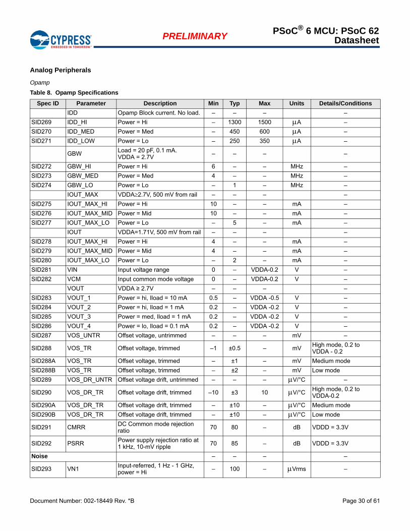
Analog Peripherals
Opamp
Table 8. Opamp Specifications
Spec ID Parameter Description Min Typ Max Units Details/Conditions
IDD Opamp Block current. No load. – – – –
SID269 IDD_HI Power = Hi – 1300 1500 A –
SID270 IDD_MED Power = Med – 450 600 A –
SID271 IDD_LOW Power = Lo – 250 350 A –
GBW Load = 20 pF, 0.1 mA. VDDA = 2.7V
– – – –
SID272 GBW_HI Power = Hi 6 – – MHz –
SID273 GBW_MED Power = Med 4 – – MHz –
SID274 GBW_LO Power = Lo – 1 – MHz –
IOUT_MAX VDDA2.7V, 500 mV from rail – – – –
SID275 IOUT_MAX_HI Power = Hi 10 – – mA –
SID276 IOUT_MAX_MID Power = Mid 10 – – mA –
SID277 IOUT_MAX_LO Power = Lo – 5 – mA –
IOUT VDDA=1.71V, 500 mV from rail – – – –
SID278 IOUT_MAX_HI Power = Hi 4 – – mA –
SID279 IOUT_MAX_MID Power = Mid 4 – – mA –
SID280 IOUT_MAX_LO Power = Lo – 2 – mA –
SID281 VIN Input voltage range 0 – VDDA-0.2 V –
SID282 VCM Input common mode voltage 0 – VDDA-0.2 V –
VOUT VDDA ≥ 2.7V – – – –
SID283 VOUT_1 Power = hi, Iload = 10 mA 0.5 – VDDA -0.5 V –
SID284 VOUT_2 Power = hi, Iload = 1 mA 0.2 – VDDA -0.2 V –
SID285 VOUT_3 Power = med, Iload = 1 mA 0.2 – VDDA -0.2 V –
SID286 VOUT_4 Power = lo, Iload = 0.1 mA 0.2 – VDDA -0.2 V –
SID287 VOS_UNTR Offset voltage, untrimmed – – – mV –
SID288 VOS_TR Offset voltage, trimmed –1 ±0.5 – mVHigh mode, 0.2 to VDDA - 0.2
SID288A VOS_TR Offset voltage, trimmed – ±1 – mV Medium mode
SID288B VOS_TR Offset voltage, trimmed – ±2 – mV Low mode
SID289 VOS_DR_UNTR Offset voltage drift, untrimmed – – – V/°C –
SID290 VOS_DR_TR Offset voltage drift, trimmed –10 ±3 10 V/°CHigh mode, 0.2 to VDDA-0.2
SID290A VOS_DR_TR Offset voltage drift, trimmed – ±10 – V/°C Medium mode
SID290B VOS_DR_TR Offset voltage drift, trimmed – ±10 – V/°C Low mode
SID291 CMRR DC Common mode rejection ratio
70 80 – dB VDDD = 3.3V
SID292 PSRRPower supply rejection ratio at 1 kHz, 10-mV ripple 70 85 – dB VDDD = 3.3V
Noise – – – –
SID293 VN1 Input-referred, 1 Hz - 1 GHz, power = Hi – 100 – Vrms –
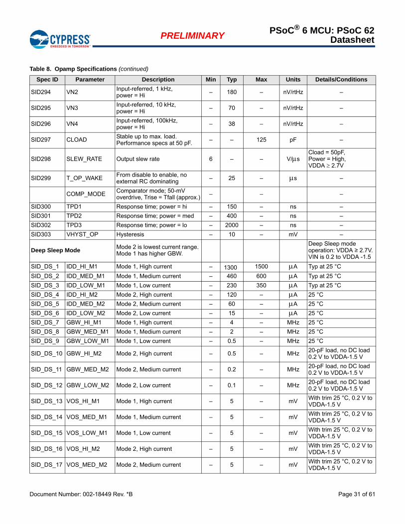
Document Number: 002-18449 Rev. *B Page 31 of 61
PRELIMINARYPSoC® 6 MCU: PSoC 62
Datasheet
SID294 VN2 Input-referred, 1 kHz, power = Hi – 180 – nV/rtHz –
SID295 VN3 Input-referred, 10 kHz, power = Hi
– 70 – nV/rtHz –
SID296 VN4 Input-referred, 100kHz, power = Hi
– 38 – nV/rtHz –
SID297 CLOAD Stable up to max. load. Performance specs at 50 pF.
– – 125 pF –
SID298 SLEW_RATE Output slew rate 6 – – V/sCload = 50pF, Power = High, VDDA 2.7V
SID299 T_OP_WAKE From disable to enable, no external RC dominating – 25 – s –
COMP_MODE Comparator mode; 50-mV overdrive, Trise = Tfall (approx.) – – –
SID300 TPD1 Response time; power = hi – 150 – ns –
SID301 TPD2 Response time; power = med – 400 – ns –
SID302 TPD3 Response time; power = lo – 2000 – ns –
SID303 VHYST_OP Hysteresis – 10 – mV –
Deep Sleep ModeMode 2 is lowest current range. Mode 1 has higher GBW.
Deep Sleep mode operation: VDDA ≥ 2.7V. VIN is 0.2 to VDDA -1.5
SID_DS_1 IDD_HI_M1 Mode 1, High current – 1300 1500 A Typ at 25 °C
SID_DS_2 IDD_MED_M1 Mode 1, Medium current – 460 600 A Typ at 25 °C
SID_DS_3 IDD_LOW_M1 Mode 1, Low current – 230 350 A Typ at 25 °C
SID_DS_4 IDD_HI_M2 Mode 2, High current – 120 – A 25 °C
SID_DS_5 IDD_MED_M2 Mode 2, Medium current – 60 – A 25 °C
SID_DS_6 IDD_LOW_M2 Mode 2, Low current – 15 – A 25 °C
SID_DS_7 GBW_HI_M1 Mode 1, High current – 4 – MHz 25 °C
SID_DS_8 GBW_MED_M1 Mode 1, Medium current – 2 – MHz 25 °C
SID_DS_9 GBW_LOW_M1 Mode 1, Low current – 0.5 – MHz 25 °C
SID_DS_10 GBW_HI_M2 Mode 2, High current – 0.5 – MHz 20-pF load, no DC load 0.2 V to VDDA-1.5 V
SID_DS_11 GBW_MED_M2 Mode 2, Medium current – 0.2 – MHz 20-pF load, no DC load 0.2 V to VDDA-1.5 V
SID_DS_12 GBW_LOW_M2 Mode 2, Low current – 0.1 – MHz 20-pF load, no DC load 0.2 V to VDDA-1.5 V
SID_DS_13 VOS_HI_M1 Mode 1, High current – 5 – mV With trim 25 °C, 0.2 V to VDDA-1.5 V
SID_DS_14 VOS_MED_M1 Mode 1, Medium current – 5 – mV With trim 25 °C, 0.2 V to VDDA-1.5 V
SID_DS_15 VOS_LOW_M1 Mode 1, Low current – 5 – mV With trim 25 °C, 0.2 V to VDDA-1.5 V
SID_DS_16 VOS_HI_M2 Mode 2, High current – 5 – mVWith trim 25 °C, 0.2 V to VDDA-1.5 V
SID_DS_17 VOS_MED_M2 Mode 2, Medium current – 5 – mVWith trim 25 °C, 0.2 V to VDDA-1.5 V
Table 8. Opamp Specifications (continued)
Spec ID Parameter Description Min Typ Max Units Details/Conditions
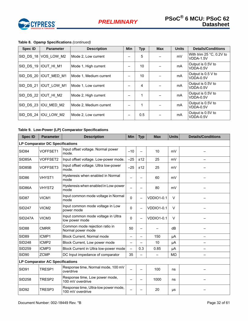
Document Number: 002-18449 Rev. *B Page 32 of 61
PRELIMINARYPSoC® 6 MCU: PSoC 62
Datasheet
SID_DS_18 VOS_LOW_M2 Mode 2, Low current – 5 – mV With trim 25 °C, 0.2V to VDDA-1.5V
SID_DS_19 IOUT_HI_M1 Mode 1, High current – 10 – mA Output is 0.5V to VDDA-0.5V
SID_DS_20 IOUT_MED_M1 Mode 1, Medium current – 10 – mA Output is 0.5 V to VDDA-0.5V
SID_DS_21 IOUT_LOW_M1 Mode 1, Low current – 4 – mA Output is 0.5V to VDDA-0.5V
SID_DS_22 IOUT_HI_M2 Mode 2, High current – 1 – mA Output is 0.5V to VDDA-0.5V
SID_DS_23 IOU_MED_M2 Mode 2, Medium current – 1 – mA Output is 0.5V to VDDA-0.5V
SID_DS_24 IOU_LOW_M2 Mode 2, Low current – 0.5 – mA Output is 0.5V to VDDA-0.5V
Table 8. Opamp Specifications (continued)
Spec ID Parameter Description Min Typ Max Units Details/Conditions
Table 9. Low-Power (LP) Comparator Specifications
Spec ID Parameter Description Min Typ Max Units Details/Conditions
LP Comparator DC Specifications
SID84 VOFFSET1 Input offset voltage. Normal power mode. –10 – 10 mV –
SID85A VOFFSET2 Input offset voltage. Low-power mode. –25 ±12 25 mV –
SID85B VOFFSET3Input offset voltage. Ultra low-power mode. –25 ±12 25 mV –
SID86 VHYST1 Hysteresis when enabled in Normal mode
– – 60 mV –
SID86A VHYST2 Hysteresis when enabled in Low-power mode – – 80 mV –
SID87 VICM1Input common mode voltage in Normal mode 0 – VDDIO1-0.1 V –
SID247 VICM2 Input common mode voltage in Low power mode
0 – VDDIO1-0.1 V –
SID247A VICM3 Input common mode voltage in Ultra low power mode 0 – VDDIO1-0.1 V –
SID88 CMRRCommon mode rejection ratio in Normal power mode 50 – – dB –
SID89 ICMP1 Block Current, Normal mode – – 150 µA –
SID248 ICMP2 Block Current, Low power mode – – 10 µA –
SID259 ICMP3 Block Current in Ultra low-power mode – 0.3 0.85 µA –
SID90 ZCMP DC Input impedance of comparator 35 – – MΩ –
LP Comparator AC Specifications
SID91 TRESP1Response time, Normal mode, 100 mV overdrive – – 100 ns –
SID258 TRESP2 Response time, Low power mode, 100 mV overdrive
– – 1000 ns –
SID92 TRESP3 Response time, Ultra-low power mode, 100 mV overdrive
– – 20 µs –
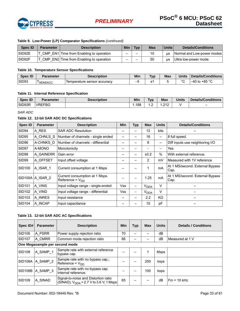
Document Number: 002-18449 Rev. *B Page 33 of 61
PRELIMINARYPSoC® 6 MCU: PSoC 62
Datasheet
SAR ADC
SID92E T_CMP_EN1 Time from Enabling to operation – – 10 µs Normal and Low-power modes
SID92F T_CMP_EN2 Time from Enabling to operation – – 50 µs Ultra low-power mode
Table 9. Low-Power (LP) Comparator Specifications (continued)
Spec ID Parameter Description Min Typ Max Units Details/Conditions
Table 10. Temperature Sensor Specifications
Spec ID Parameter Description Min Typ Max Units Details/Conditions
SID93 TSENSACC Temperature sensor accuracy –5 ±1 5 °C –40 to +85 °C
Table 11. Internal Reference Specification
Spec ID Parameter Description Min Typ Max Units Details/Conditions
SID93R VREFBG 1.188 1.2 1.212 V –
Table 12. 12-bit SAR ADC DC Specifications
Spec ID Parameter Description Min Typ Max Units Details/Conditions
SID94 A_RES SAR ADC Resolution – – 12 bits –
SID95 A_CHNLS_S Number of channels - single ended – – 16 – 8 full speed.
SID96 A-CHNKS_D Number of channels - differential – – 8 – Diff inputs use neighboring I/O
SID97 A-MONO Monotonicity – – - – Yes
SID98 A_GAINERR Gain error – – ±0.2 % With external reference.
SID99 A_OFFSET Input offset voltage – – 2 mV Measured with 1V reference
SID100 A_ISAR_1 Current consumption at 1 Msps – – 1 mAAt 1 MS/second. External Bypass Cap.
SID100A A_ISAR_2 Current consumption at 1 Msps. Reference = VDD
– – 1.25 mA At 1 MS/second. External Bypass Cap.
SID101 A_VINS Input voltage range - single-ended Vss – VDDA V –
SID102 A_VIND Input voltage range - differential Vss – VDDA V –
SID103 A_INRES Input resistance – – 2.2 KΩ –
SID104 A_INCAP Input capacitance – – 10 pF –
Table 13. 12-bit SAR ADC AC Specifications
Spec ID# Parameter Description Min Typ Max Units Details / Conditions
SID106 A_PSRR Power supply rejection ratio 70 – – dB
SID107 A_CMRR Common mode rejection ratio 66 – – dB Measured at 1 V
One Megasample per second mode
SID108 A_SAMP_1 Sample rate with external reference bypass cap.
– – 1 Msps
SID108A A_SAMP_2Sample rate with no bypass cap.; Reference = VDD
– – 250 ksps
SID108B A_SAMP_3Sample rate with no bypass cap. Internal reference. – – 100 ksps
SID109 A_SINAD Signal-to-noise and Distortion ratio (SINAD). VDDA = 2.7 V to 3.6 V, 1 Msps
65 – – dB Fin = 10 kHz
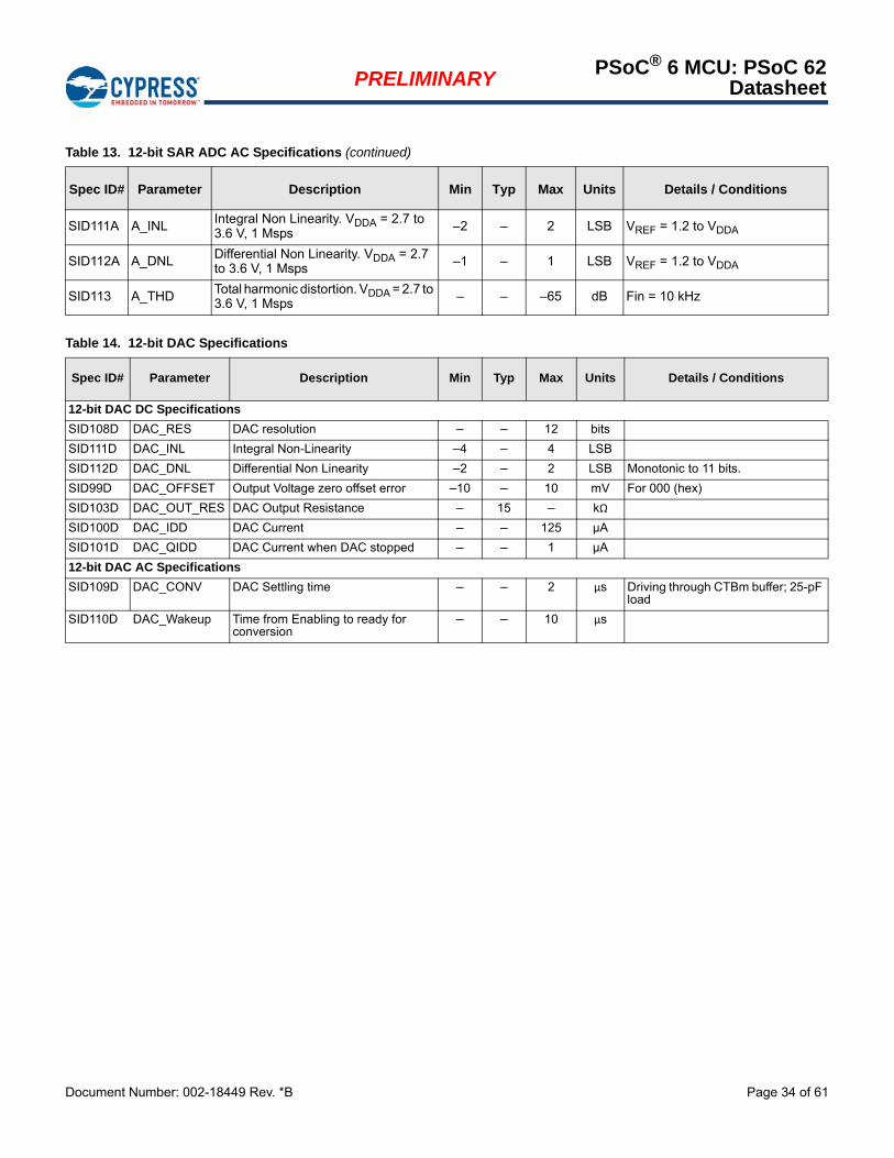
Document Number: 002-18449 Rev. *B Page 34 of 61
PRELIMINARYPSoC® 6 MCU: PSoC 62
Datasheet
SID111A A_INLIntegral Non Linearity. VDDA = 2.7 to 3.6 V, 1 Msps –2 – 2 LSB VREF = 1.2 to VDDA
SID112A A_DNL Differential Non Linearity. VDDA = 2.7 to 3.6 V, 1 Msps –1 – 1 LSB VREF = 1.2 to VDDA
SID113 A_THD Total harmonic distortion. VDDA = 2.7 to 3.6 V, 1 Msps – – –65 dB Fin = 10 kHz
Table 13. 12-bit SAR ADC AC Specifications (continued)
Spec ID# Parameter Description Min Typ Max Units Details / Conditions
Table 14. 12-bit DAC Specifications
Spec ID# Parameter Description Min Typ Max Units Details / Conditions
12-bit DAC DC Specifications
SID108D DAC_RES DAC resolution – – 12 bits
SID111D DAC_INL Integral Non-Linearity –4 – 4 LSB
SID112D DAC_DNL Differential Non Linearity –2 – 2 LSB Monotonic to 11 bits.
SID99D DAC_OFFSET Output Voltage zero offset error –10 – 10 mV For 000 (hex)
SID103D DAC_OUT_RES DAC Output Resistance – 15 – kΩ
SID100D DAC_IDD DAC Current – – 125 µA
SID101D DAC_QIDD DAC Current when DAC stopped – – 1 µA
12-bit DAC AC Specifications
SID109D DAC_CONV DAC Settling time – – 2 µs Driving through CTBm buffer; 25-pF load
SID110D DAC_Wakeup Time from Enabling to ready for conversion
– – 10 µs
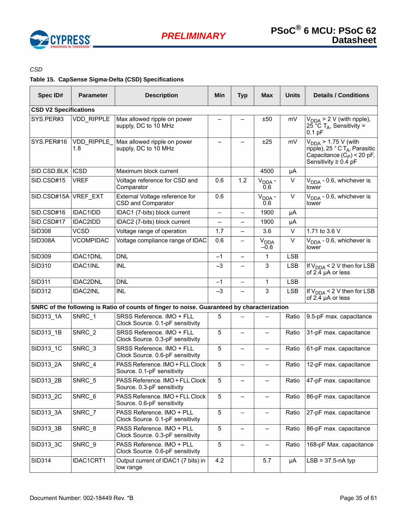
Document Number: 002-18449 Rev. *B Page 35 of 61
PRELIMINARYPSoC® 6 MCU: PSoC 62
Datasheet
CSD
Table 15. CapSense Sigma-Delta (CSD) Specifications
Spec ID# Parameter Description Min Typ Max Units Details / Conditions
CSD V2 Specifications
SYS.PER#3 VDD_RIPPLE Max allowed ripple on power supply, DC to 10 MHz
– – ±50 mV VDDA > 2 V (with ripple), 25 °C TA, Sensitivity = 0.1 pF
SYS.PER#16 VDD_RIPPLE_1.8
Max allowed ripple on power supply, DC to 10 MHz
– – ±25 mV VDDA > 1.75 V (with ripple), 25 ° C TA, Parasitic Capacitance (CP) < 20 pF, Sensitivity ≥ 0.4 pF
SID.CSD.BLK ICSD Maximum block current 4500 µA
SID.CSD#15 VREF Voltage reference for CSD and Comparator
0.6 1.2 VDDA - 0.6
V VDDA - 0.6, whichever is lower
SID.CSD#15A VREF_EXT External Voltage reference for CSD and Comparator
0.6 VDDA - 0.6
V VDDA - 0.6, whichever is lower
SID.CSD#16 IDAC1IDD IDAC1 (7-bits) block current – – 1900 µA
SID.CSD#17 IDAC2IDD IDAC2 (7-bits) block current – – 1900 µA
SID308 VCSD Voltage range of operation 1.7 – 3.6 V 1.71 to 3.6 V
SID308A VCOMPIDAC Voltage compliance range of IDAC 0.6 – VDDA –0.6
V VDDA - 0.6, whichever is lower
SID309 IDAC1DNL DNL –1 – 1 LSB
SID310 IDAC1INL INL –3 – 3 LSB If VDDA < 2 V then for LSB of 2.4 µA or less
SID311 IDAC2DNL DNL –1 – 1 LSB
SID312 IDAC2INL INL –3 – 3 LSB If VDDA < 2 V then for LSB of 2.4 µA or less
SNRC of the following is Ratio of counts of finger to noise. Guaranteed by characterization
SID313_1A SNRC_1 SRSS Reference. IMO + FLL Clock Source. 0.1-pF sensitivity
5 – – Ratio 9.5-pF max. capacitance
SID313_1B SNRC_2 SRSS Reference. IMO + FLL Clock Source. 0.3-pF sensitivity
5 – – Ratio 31-pF max. capacitance
SID313_1C SNRC_3 SRSS Reference. IMO + FLL Clock Source. 0.6-pF sensitivity
5 – – Ratio 61-pF max. capacitance
SID313_2A SNRC_4 PASS Reference. IMO + FLL Clock Source. 0.1-pF sensitivity
5 – – Ratio 12-pF max. capacitance
SID313_2B SNRC_5 PASS Reference. IMO + FLL Clock Source. 0.3-pF sensitivity
5 – – Ratio 47-pF max. capacitance
SID313_2C SNRC_6 PASS Reference. IMO + FLL Clock Source. 0.6-pF sensitivity
5 – – Ratio 86-pF max. capacitance
SID313_3A SNRC_7 PASS Reference. IMO + PLL Clock Source. 0.1-pF sensitivity
5 – – Ratio 27-pF max. capacitance
SID313_3B SNRC_8 PASS Reference. IMO + PLL Clock Source. 0.3-pF sensitivity
5 – – Ratio 86-pF max. capacitance
SID313_3C SNRC_9 PASS Reference. IMO + PLL Clock Source. 0.6-pF sensitivity
5 – – Ratio 168-pF Max. capacitance
SID314 IDAC1CRT1 Output current of IDAC1 (7 bits) in low range
4.2 5.7 µA LSB = 37.5-nA typ
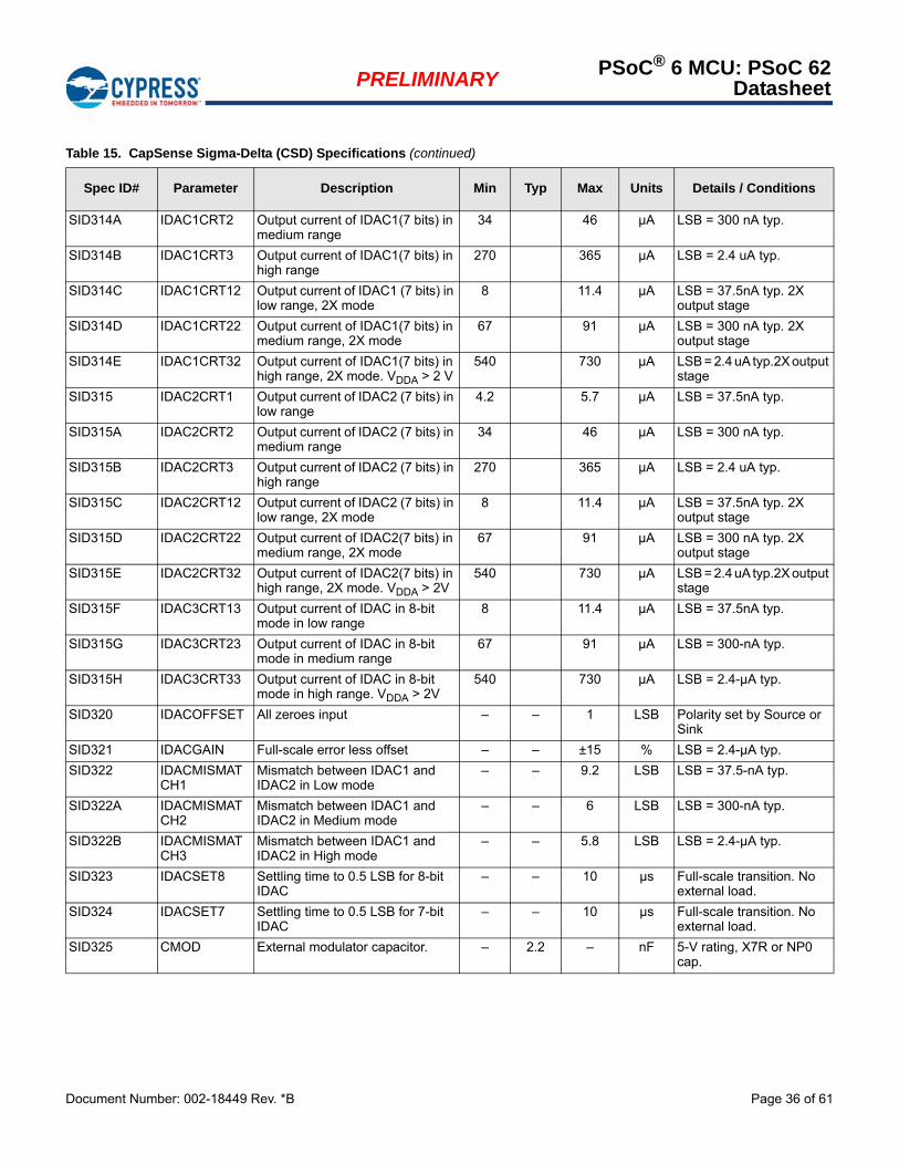
Document Number: 002-18449 Rev. *B Page 36 of 61
PRELIMINARYPSoC® 6 MCU: PSoC 62
Datasheet
SID314A IDAC1CRT2 Output current of IDAC1(7 bits) in medium range
34 46 µA LSB = 300 nA typ.
SID314B IDAC1CRT3 Output current of IDAC1(7 bits) in high range
270 365 µA LSB = 2.4 uA typ.
SID314C IDAC1CRT12 Output current of IDAC1 (7 bits) in low range, 2X mode
8 11.4 µA LSB = 37.5nA typ. 2X output stage
SID314D IDAC1CRT22 Output current of IDAC1(7 bits) in medium range, 2X mode
67 91 µA LSB = 300 nA typ. 2X output stage
SID314E IDAC1CRT32 Output current of IDAC1(7 bits) in high range, 2X mode. VDDA > 2 V
540 730 µA LSB = 2.4 uA typ.2X output stage
SID315 IDAC2CRT1 Output current of IDAC2 (7 bits) in low range
4.2 5.7 µA LSB = 37.5nA typ.
SID315A IDAC2CRT2 Output current of IDAC2 (7 bits) in medium range
34 46 µA LSB = 300 nA typ.
SID315B IDAC2CRT3 Output current of IDAC2 (7 bits) in high range
270 365 µA LSB = 2.4 uA typ.
SID315C IDAC2CRT12 Output current of IDAC2 (7 bits) in low range, 2X mode
8 11.4 µA LSB = 37.5nA typ. 2X output stage
SID315D IDAC2CRT22 Output current of IDAC2(7 bits) in medium range, 2X mode
67 91 µA LSB = 300 nA typ. 2X output stage
SID315E IDAC2CRT32 Output current of IDAC2(7 bits) in high range, 2X mode. VDDA > 2V
540 730 µA LSB = 2.4 uA typ.2X output stage
SID315F IDAC3CRT13 Output current of IDAC in 8-bit mode in low range
8 11.4 µA LSB = 37.5nA typ.
SID315G IDAC3CRT23 Output current of IDAC in 8-bit mode in medium range
67 91 µA LSB = 300-nA typ.
SID315H IDAC3CRT33 Output current of IDAC in 8-bit mode in high range. VDDA > 2V
540 730 µA LSB = 2.4-µA typ.
SID320 IDACOFFSET All zeroes input – – 1 LSB Polarity set by Source or Sink
SID321 IDACGAIN Full-scale error less offset – – ±15 % LSB = 2.4-µA typ.
SID322 IDACMISMATCH1
Mismatch between IDAC1 and IDAC2 in Low mode
– – 9.2 LSB LSB = 37.5-nA typ.
SID322A IDACMISMATCH2
Mismatch between IDAC1 and IDAC2 in Medium mode
– – 6 LSB LSB = 300-nA typ.
SID322B IDACMISMATCH3
Mismatch between IDAC1 and IDAC2 in High mode
– – 5.8 LSB LSB = 2.4-µA typ.
SID323 IDACSET8 Settling time to 0.5 LSB for 8-bit IDAC
– – 10 µs Full-scale transition. No external load.
SID324 IDACSET7 Settling time to 0.5 LSB for 7-bit IDAC
– – 10 µs Full-scale transition. No external load.
SID325 CMOD External modulator capacitor. – 2.2 – nF 5-V rating, X7R or NP0 cap.
Table 15. CapSense Sigma-Delta (CSD) Specifications (continued)
Spec ID# Parameter Description Min Typ Max Units Details / Conditions
Document Number: 002-18449 Rev. *B Page 37 of 61
PRELIMINARYPSoC® 6 MCU: PSoC 62
Datasheet
Table 16. CSD ADC Specifications
Spec ID Parameter Description Min Typ Max Units Details/Conditions
SIDA94 A_RES Resolution – – 10 bits Auto-zeroing is required every millisecond
SIDA95 A_CHNLS_S Number of channels - single ended
– – 16 Defined by AMUX Bus
SIDA97 A-MONO Monotonicity – – – Yes –
SIDA98 A_GAINERR Gain error – – TBD % –
SIDA99 A_OFFSET Input offset voltage – – TBD mV –
SIDA100 A_ISAR Current consumption – – TBD mA –
SIDA101 A_VINSInput voltage range - single ended VSSA – VDDA V –
SIDA103 A_INRES Input resistance – 2.2 – KΩ –
SIDA104 A_INCAP Input capacitance – 20 – pF –
SIDA106 A_PSRR Power supply rejection ratio TBD – – dB –
SIDA107 A_TACQ Sample acquisition time – 1 – s –
SIDA108 A_CONV8
Conversion time for 8-bit resolution at conversion rate = Fhclk/(2^(N+2)). Clock frequency = 48 MHz.
– – 21.3 sDoes not include acquisition time. Equivalent to 44.8 ksps including acquisition time.
SIDA108A A_CONV10
Conversion time for 10-bit resolution at conversion rate = Fhclk/(2^(N+2)). Clock frequency = 48 MHz.
– – 85.3 sDoes not include acquisition time. Equivalent to 11.6 ksps including acquisition time.
SIDA109 A_SNDSignal-to-noise and Distortion ratio (SINAD) TBD – – dB –
SIDA110 A_BW Input bandwidth without aliasing – – 22.4 kHz 8-bit resolution
SIDA111 A_INL Integral Non Linearity. 1 ksps – – 2 LSB Vref = 2.4 V or greater
SIDA112 A_DNL Differential Non Linearity. 1 ksps – – 1 LSB –
Document Number: 002-18449 Rev. *B Page 38 of 61
PRELIMINARYPSoC® 6 MCU: PSoC 62
Datasheet
Digital Peripherals
Table 17. Timer/Counter/PWM (TCPWM) Specifications
Spec ID Parameter Description Min Typ Max Units Details/Conditions
SID.TCPWM.1 ITCPWM1 Block current consumption at 8 MHz – – 70 A All modes (TCPWM)
SID.TCPWM.2 ITCPWM2 Block current consumption at 24 MHz – – 180 A All modes (TCPWM)
SID.TCPWM.2A ITCPWM3 Block current consumption at 50 MHz – – 270 A All modes (TCPWM)
SID.TCPWM.2B ITCPWM4 Block current consumption at 100 MHz – – 540 A All modes (TCPWM)
SID.TCPWM.3 TCPWMFREQ Operating frequency – – 100 MHz Fc max = FcpuMaximum = 100 MHz
SID.TCPWM.4 TPWMENEXT Input Trigger Pulse Width for all Trigger Events
2/Fc – – ns
Trigger Events can be Stop, Start, Reload, Count, Capture, or Kill depending on which mode of operation is selected.
SID.TCPWM.5 TPWMEXT Output Trigger Pulse widths 1.5/Fc – – ns
Minimum possible width of Overflow, Underflow, and CC (Counter equals Compare value) trigger outputs
SID.TCPWM.5A TCRES Resolution of Counter 1/Fc – – nsMinimum time between successive counts
SID.TCPWM.5B PWMRES PWM Resolution 1/Fc – – nsMinimum pulse width of PWM Output
SID.TCPWM.5C QRES Quadrature inputs resolution 2/Fc – – ns
Minimum pulse width between Quadrature phase inputs. Delays from pins should be similar.
Table 18. Serial Communication Block (SCB) Specifications
Spec ID# Parameter Description Min Typ Max Units Details / Conditions
Fixed I2C DC Specifications
SID149 II2C1 Block current consumption at 100 kHz - - 30 µA
SID150 II2C2 Block current consumption at 400 kHz - - 80 µA
SID151 II2C3 Block current consumption at 1 Mbps - - 180 µA
SID152 II2C4 I2C enabled in Deep Sleep mode - - 1.4 µA
Fixed I2C AC Specifications
SID153 FI2C1 Bit Rate - - 1 Mbps
Fixed UART DC Specifications
SID160 IUART1 Block current consumption at 100 Kbps - - 30 µA
SID161 IUART2 Block current consumption at 1000 Kbps - - 180 µA
Fixed UART AC Specifications
SID162 FUART Bit Rate 1 Mbps
Fixed SPI DC Specifications
SID163 ISPI1 Block current consumption at 1Mbps - - 220 µA
SID164 ISPI2 Block current consumption at 4 Mbps - - 340 µA
SID165 ISPI3 Block current consumption at 8 Mbps - - 360 µA
SID165A ISP14 Block current consumption at 25 Mbps - - 800 µA
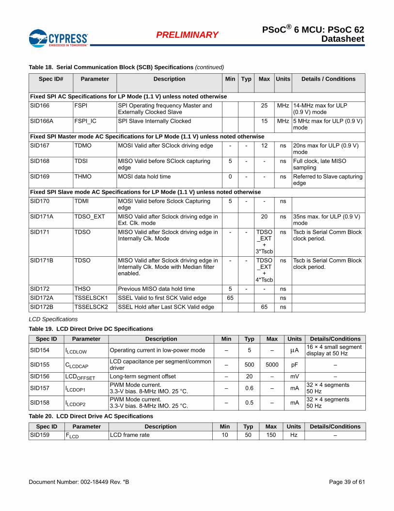
Document Number: 002-18449 Rev. *B Page 39 of 61
PRELIMINARYPSoC® 6 MCU: PSoC 62
Datasheet
LCD Specifications
Fixed SPI AC Specifications for LP Mode (1.1 V) unless noted otherwise
SID166 FSPI SPI Operating frequency Master and Externally Clocked Slave
25 MHz 14-MHz max for ULP (0.9 V) mode
SID166A FSPI_IC SPI Slave Internally Clocked 15 MHz 5 MHz max for ULP (0.9 V) mode
Fixed SPI Master mode AC Specifications for LP Mode (1.1 V) unless noted otherwise
SID167 TDMO MOSI Valid after SClock driving edge - - 12 ns 20ns max for ULP (0.9 V) mode
SID168 TDSI MISO Valid before SClock capturing edge
5 - - ns Full clock, late MISO sampling
SID169 THMO MOSI data hold time 0 - - ns Referred to Slave capturing edge
Fixed SPI Slave mode AC Specifications for LP Mode (1.1 V) unless noted otherwise
SID170 TDMI MOSI Valid before Sclock Capturing edge
5 - - ns
SID171A TDSO_EXT MISO Valid after Sclock driving edge in Ext. Clk. mode
20 ns 35ns max. for ULP (0.9 V) mode
SID171 TDSO MISO Valid after Sclock driving edge in Internally Clk. Mode
- - TDSO_EXT
+ 3*Tscb
ns Tscb is Serial Comm Block clock period.
SID171B TDSO MISO Valid after Sclock driving edge in Internally Clk. Mode with Median filter enabled.
- - TDSO_EXT
+ 4*Tscb
ns Tscb is Serial Comm Block clock period.
SID172 THSO Previous MISO data hold time 5 - - ns
SID172A TSSELSCK1 SSEL Valid to first SCK Valid edge 65 ns
SID172B TSSELSCK2 SSEL Hold after Last SCK Valid edge 65 ns
Table 19. LCD Direct Drive DC Specifications
Spec ID Parameter Description Min Typ Max Units Details/Conditions
SID154 ILCDLOW Operating current in low-power mode – 5 – A16 × 4 small segment display at 50 Hz
SID155 CLCDCAPLCD capacitance per segment/common driver – 500 5000 pF –
SID156 LCDOFFSET Long-term segment offset – 20 – mV –
SID157 ILCDOP1PWM Mode current. 3.3-V bias. 8-MHz IMO. 25 °C. – 0.6 – mA
32 × 4 segments50 Hz
SID158 ILCDOP2PWM Mode current. 3.3-V bias. 8-MHz IMO. 25 °C. – 0.5 – mA
32 × 4 segments50 Hz
Table 20. LCD Direct Drive AC Specifications
Spec ID Parameter Description Min Typ Max Units Details/Conditions
SID159 FLCD LCD frame rate 10 50 150 Hz –
Table 18. Serial Communication Block (SCB) Specifications (continued)
Spec ID# Parameter Description Min Typ Max Units Details / Conditions
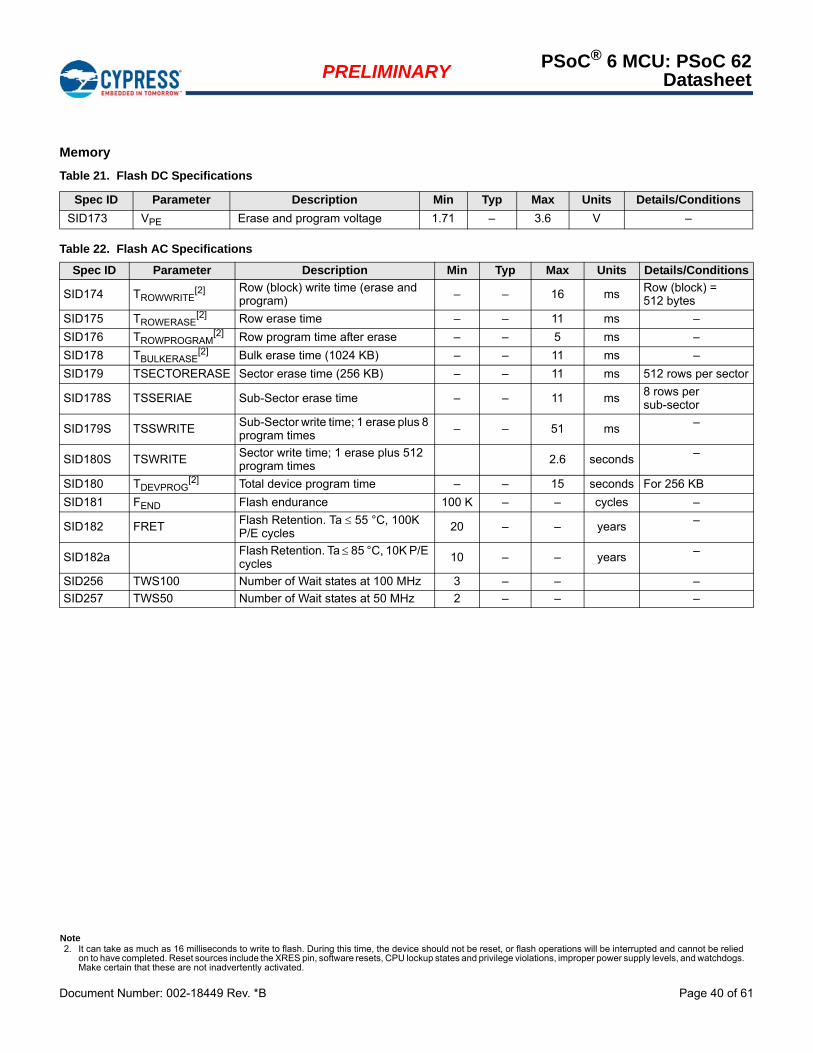
Document Number: 002-18449 Rev. *B Page 40 of 61
PRELIMINARYPSoC® 6 MCU: PSoC 62
Datasheet
Memory
Table 21. Flash DC Specifications
Spec ID Parameter Description Min Typ Max Units Details/Conditions
SID173 VPE Erase and program voltage 1.71 – 3.6 V –
Table 22. Flash AC Specifications
Spec ID Parameter Description Min Typ Max Units Details/Conditions
SID174 TROWWRITE[2] Row (block) write time (erase and
program) – – 16 ms Row (block) = 512 bytes
SID175 TROWERASE[2] Row erase time – – 11 ms –
SID176 TROWPROGRAM[2] Row program time after erase – – 5 ms –
SID178 TBULKERASE[2] Bulk erase time (1024 KB) – – 11 ms –
SID179 TSECTORERASE Sector erase time (256 KB) – – 11 ms 512 rows per sector
SID178S TSSERIAE Sub-Sector erase time – – 11 ms 8 rows per sub-sector
SID179S TSSWRITESub-Sector write time; 1 erase plus 8 program times – – 51 ms
–
SID180S TSWRITE Sector write time; 1 erase plus 512 program times 2.6 seconds –
SID180 TDEVPROG[2] Total device program time – – 15 seconds For 256 KB
SID181 FEND Flash endurance 100 K – – cycles –
SID182 FRET Flash Retention. Ta 55 °C, 100K P/E cycles
20 – – years –
SID182aFlash Retention. Ta 85 °C, 10K P/E cycles 10 – – years
–
SID256 TWS100 Number of Wait states at 100 MHz 3 – – –
SID257 TWS50 Number of Wait states at 50 MHz 2 – – –
Note2. It can take as much as 16 milliseconds to write to flash. During this time, the device should not be reset, or flash operations will be interrupted and cannot be relied
on to have completed. Reset sources include the XRES pin, software resets, CPU lockup states and privilege violations, improper power supply levels, and watchdogs. Make certain that these are not inadvertently activated.
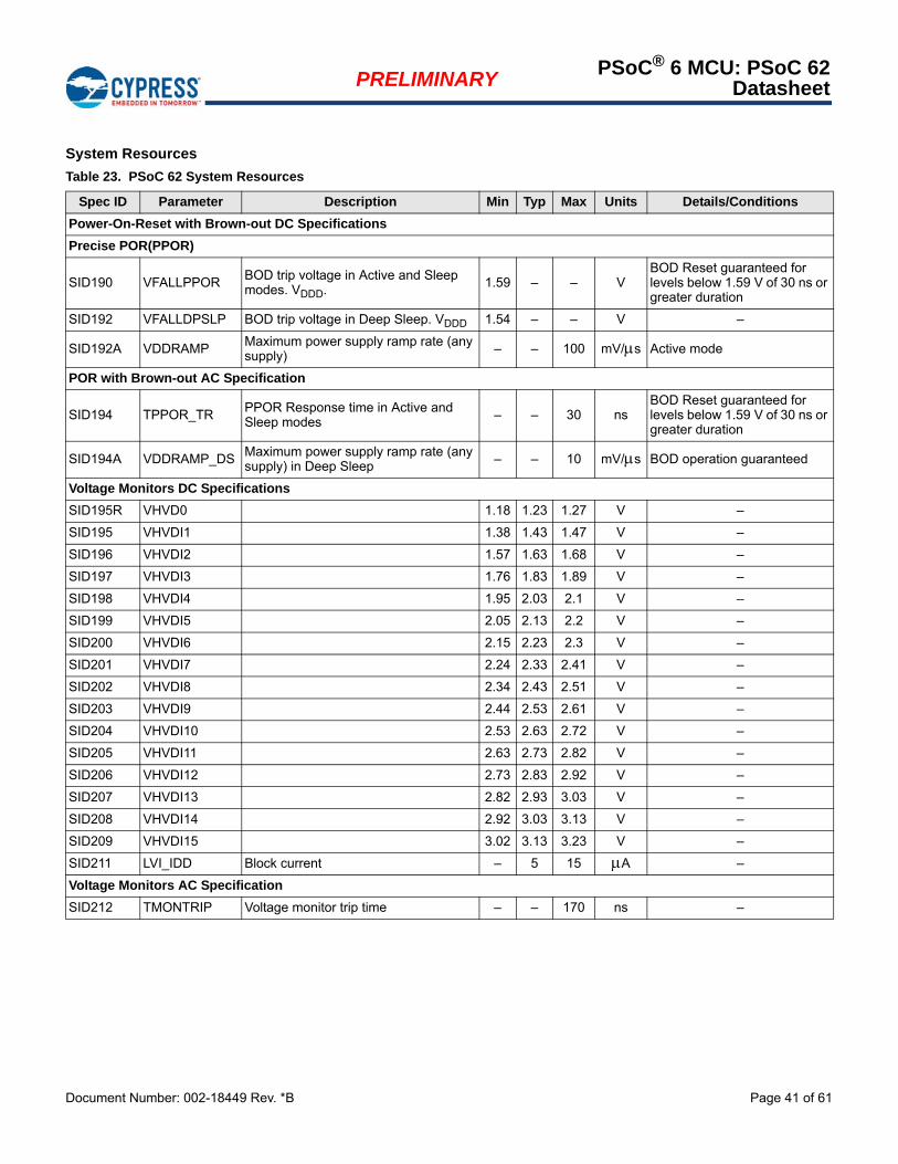
Document Number: 002-18449 Rev. *B Page 41 of 61
PRELIMINARYPSoC® 6 MCU: PSoC 62
Datasheet
System Resources
Table 23. PSoC 62 System Resources
Spec ID Parameter Description Min Typ Max Units Details/Conditions
Power-On-Reset with Brown-out DC Specifications
Precise POR(PPOR)
SID190 VFALLPPORBOD trip voltage in Active and Sleep modes. VDDD. 1.59 – – V
BOD Reset guaranteed for levels below 1.59 V of 30 ns or greater duration
SID192 VFALLDPSLP BOD trip voltage in Deep Sleep. VDDD 1.54 – – V –
SID192A VDDRAMPMaximum power supply ramp rate (any supply) – – 100 mV/s Active mode
POR with Brown-out AC Specification
SID194 TPPOR_TRPPOR Response time in Active and Sleep modes – – 30 ns
BOD Reset guaranteed for levels below 1.59 V of 30 ns or greater duration
SID194A VDDRAMP_DSMaximum power supply ramp rate (any supply) in Deep Sleep – – 10 mV/s BOD operation guaranteed
Voltage Monitors DC Specifications
SID195R VHVD0 1.18 1.23 1.27 V –
SID195 VHVDI1 1.38 1.43 1.47 V –
SID196 VHVDI2 1.57 1.63 1.68 V –
SID197 VHVDI3 1.76 1.83 1.89 V –
SID198 VHVDI4 1.95 2.03 2.1 V –
SID199 VHVDI5 2.05 2.13 2.2 V –
SID200 VHVDI6 2.15 2.23 2.3 V –
SID201 VHVDI7 2.24 2.33 2.41 V –
SID202 VHVDI8 2.34 2.43 2.51 V –
SID203 VHVDI9 2.44 2.53 2.61 V –
SID204 VHVDI10 2.53 2.63 2.72 V –
SID205 VHVDI11 2.63 2.73 2.82 V –
SID206 VHVDI12 2.73 2.83 2.92 V –
SID207 VHVDI13 2.82 2.93 3.03 V –
SID208 VHVDI14 2.92 3.03 3.13 V –
SID209 VHVDI15 3.02 3.13 3.23 V –
SID211 LVI_IDD Block current – 5 15 A –
Voltage Monitors AC Specification
SID212 TMONTRIP Voltage monitor trip time – – 170 ns –
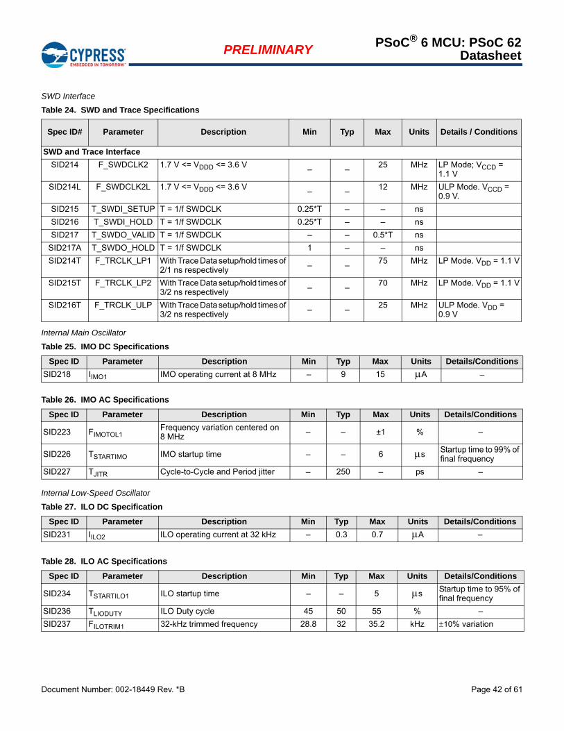
Document Number: 002-18449 Rev. *B Page 42 of 61
PRELIMINARYPSoC® 6 MCU: PSoC 62
Datasheet
SWD Interface
Internal Main Oscillator
Internal Low-Speed Oscillator
Table 24. SWD and Trace Specifications
Spec ID# Parameter Description Min Typ Max Units Details / Conditions
SWD and Trace Interface
SID214 F_SWDCLK2 1.7 V <= VDDD <= 3.6 V– –
25 MHz LP Mode; VCCD = 1.1 V
SID214L F_SWDCLK2L 1.7 V <= VDDD <= 3.6 V– –
12 MHz ULP Mode. VCCD = 0.9 V.
SID215 T_SWDI_SETUP T = 1/f SWDCLK 0.25*T – – ns
SID216 T_SWDI_HOLD T = 1/f SWDCLK 0.25*T – – ns
SID217 T_SWDO_VALID T = 1/f SWDCLK – – 0.5*T ns
SID217A T_SWDO_HOLD T = 1/f SWDCLK 1 – – ns
SID214T F_TRCLK_LP1 With Trace Data setup/hold times of 2/1 ns respectively – – 75 MHz LP Mode. VDD = 1.1 V
SID215T F_TRCLK_LP2 With Trace Data setup/hold times of 3/2 ns respectively – – 70 MHz LP Mode. VDD = 1.1 V
SID216T F_TRCLK_ULP With Trace Data setup/hold times of 3/2 ns respectively – – 25 MHz ULP Mode. VDD =
0.9 V
Table 25. IMO DC Specifications
Spec ID Parameter Description Min Typ Max Units Details/Conditions
SID218 IIMO1 IMO operating current at 8 MHz – 9 15 A –
Table 26. IMO AC Specifications
Spec ID Parameter Description Min Typ Max Units Details/Conditions
SID223 FIMOTOL1Frequency variation centered on 8 MHz – – ±1 % –
SID226 TSTARTIMO IMO startup time – – 6 sStartup time to 99% of final frequency
SID227 TJITR Cycle-to-Cycle and Period jitter – 250 – ps –
Table 27. ILO DC Specification
Spec ID Parameter Description Min Typ Max Units Details/Conditions
SID231 IILO2 ILO operating current at 32 kHz – 0.3 0.7 A –
Table 28. ILO AC Specifications
Spec ID Parameter Description Min Typ Max Units Details/Conditions
SID234 TSTARTILO1 ILO startup time – – 5 s Startup time to 95% of final frequency
SID236 TLIODUTY ILO Duty cycle 45 50 55 % –
SID237 FILOTRIM1 32-kHz trimmed frequency 28.8 32 35.2 kHz 10% variation
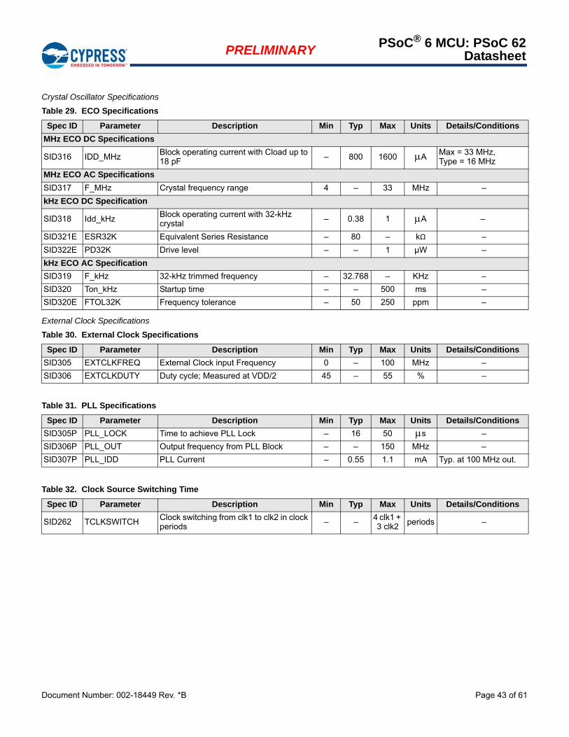
Document Number: 002-18449 Rev. *B Page 43 of 61
PRELIMINARYPSoC® 6 MCU: PSoC 62
Datasheet
Crystal Oscillator Specifications
External Clock Specifications
Table 29. ECO Specifications
Spec ID Parameter Description Min Typ Max Units Details/Conditions
MHz ECO DC Specifications
SID316 IDD_MHzBlock operating current with Cload up to 18 pF – 800 1600 A
Max = 33 MHz, Type = 16 MHz
MHz ECO AC Specifications
SID317 F_MHz Crystal frequency range 4 – 33 MHz –
kHz ECO DC Specification
SID318 Idd_kHz Block operating current with 32-kHz crystal
– 0.38 1 A –
SID321E ESR32K Equivalent Series Resistance – 80 – kΩ –
SID322E PD32K Drive level – – 1 µW –
kHz ECO AC Specification
SID319 F_kHz 32-kHz trimmed frequency – 32.768 – KHz –
SID320 Ton_kHz Startup time – – 500 ms –
SID320E FTOL32K Frequency tolerance – 50 250 ppm –
Table 30. External Clock Specifications
Spec ID Parameter Description Min Typ Max Units Details/Conditions
SID305 EXTCLKFREQ External Clock input Frequency 0 – 100 MHz –
SID306 EXTCLKDUTY Duty cycle; Measured at VDD/2 45 – 55 % –
Table 31. PLL Specifications
Spec ID Parameter Description Min Typ Max Units Details/Conditions
SID305P PLL_LOCK Time to achieve PLL Lock – 16 50 s –
SID306P PLL_OUT Output frequency from PLL Block – – 150 MHz –
SID307P PLL_IDD PLL Current – 0.55 1.1 mA Typ. at 100 MHz out.
Table 32. Clock Source Switching Time
Spec ID Parameter Description Min Typ Max Units Details/Conditions
SID262 TCLKSWITCH Clock switching from clk1 to clk2 in clock periods
– – 4 clk1 + 3 clk2
periods –
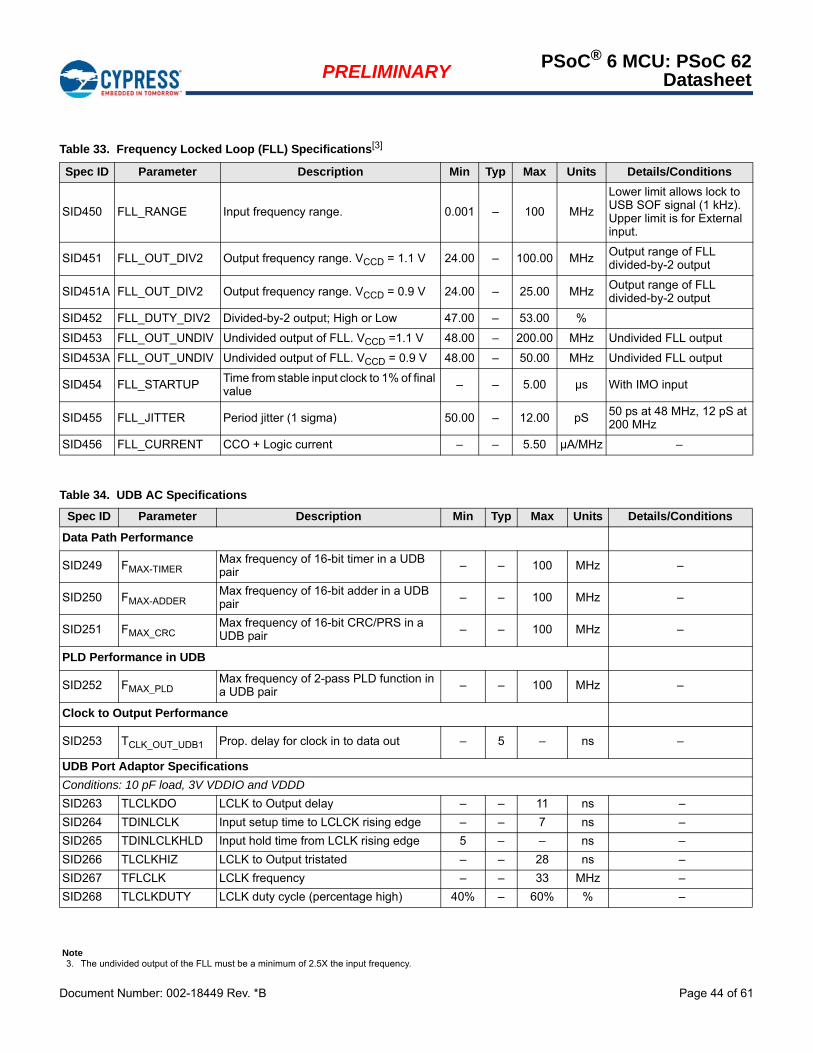
Document Number: 002-18449 Rev. *B Page 44 of 61
PRELIMINARYPSoC® 6 MCU: PSoC 62
Datasheet
Note3. The undivided output of the FLL must be a minimum of 2.5X the input frequency.
Table 33. Frequency Locked Loop (FLL) Specifications[3]
Spec ID Parameter Description Min Typ Max Units Details/Conditions
SID450 FLL_RANGE Input frequency range. 0.001 – 100 MHz
Lower limit allows lock to USB SOF signal (1 kHz). Upper limit is for External input.
SID451 FLL_OUT_DIV2 Output frequency range. VCCD = 1.1 V 24.00 – 100.00 MHz Output range of FLL divided-by-2 output
SID451A FLL_OUT_DIV2 Output frequency range. VCCD = 0.9 V 24.00 – 25.00 MHzOutput range of FLL divided-by-2 output
SID452 FLL_DUTY_DIV2 Divided-by-2 output; High or Low 47.00 – 53.00 %
SID453 FLL_OUT_UNDIV Undivided output of FLL. VCCD =1.1 V 48.00 – 200.00 MHz Undivided FLL output
SID453A FLL_OUT_UNDIV Undivided output of FLL. VCCD = 0.9 V 48.00 – 50.00 MHz Undivided FLL output
SID454 FLL_STARTUP Time from stable input clock to 1% of final value
– – 5.00 µs With IMO input
SID455 FLL_JITTER Period jitter (1 sigma) 50.00 – 12.00 pS 50 ps at 48 MHz, 12 pS at 200 MHz
SID456 FLL_CURRENT CCO + Logic current – – 5.50 µA/MHz –
Table 34. UDB AC Specifications
Spec ID Parameter Description Min Typ Max Units Details/Conditions
Data Path Performance
SID249 FMAX-TIMERMax frequency of 16-bit timer in a UDB pair – – 100 MHz –
SID250 FMAX-ADDERMax frequency of 16-bit adder in a UDB pair – – 100 MHz –
SID251 FMAX_CRCMax frequency of 16-bit CRC/PRS in a UDB pair – – 100 MHz –
PLD Performance in UDB
SID252 FMAX_PLDMax frequency of 2-pass PLD function in a UDB pair – – 100 MHz –
Clock to Output Performance
SID253 TCLK_OUT_UDB1 Prop. delay for clock in to data out – 5 – ns –
UDB Port Adaptor Specifications
Conditions: 10 pF load, 3V VDDIO and VDDD
SID263 TLCLKDO LCLK to Output delay – – 11 ns –
SID264 TDINLCLK Input setup time to LCLCK rising edge – – 7 ns –
SID265 TDINLCLKHLD Input hold time from LCLK rising edge 5 – – ns –
SID266 TLCLKHIZ LCLK to Output tristated – – 28 ns –
SID267 TFLCLK LCLK frequency – – 33 MHz –
SID268 TLCLKDUTY LCLK duty cycle (percentage high) 40% – 60% % –
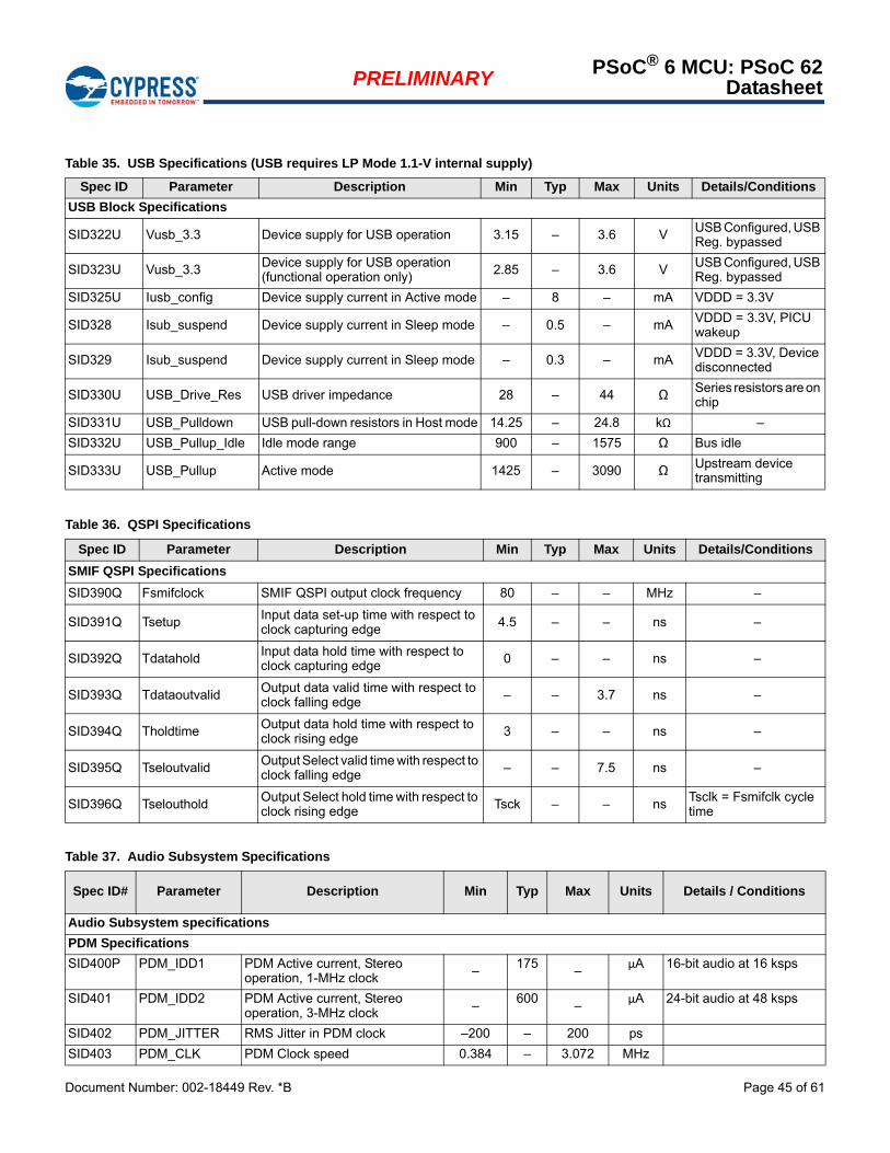
Document Number: 002-18449 Rev. *B Page 45 of 61
PRELIMINARYPSoC® 6 MCU: PSoC 62
Datasheet
Table 35. USB Specifications (USB requires LP Mode 1.1-V internal supply)
Spec ID Parameter Description Min Typ Max Units Details/Conditions
USB Block Specifications
SID322U Vusb_3.3 Device supply for USB operation 3.15 – 3.6 V USB Configured, USB Reg. bypassed
SID323U Vusb_3.3 Device supply for USB operation (functional operation only) 2.85 – 3.6 V USB Configured, USB
Reg. bypassed
SID325U Iusb_config Device supply current in Active mode – 8 – mA VDDD = 3.3V
SID328 Isub_suspend Device supply current in Sleep mode – 0.5 – mA VDDD = 3.3V, PICU wakeup
SID329 Isub_suspend Device supply current in Sleep mode – 0.3 – mA VDDD = 3.3V, Device disconnected
SID330U USB_Drive_Res USB driver impedance 28 – 44 Ω Series resistors are on chip
SID331U USB_Pulldown USB pull-down resistors in Host mode 14.25 – 24.8 kΩ –
SID332U USB_Pullup_Idle Idle mode range 900 – 1575 Ω Bus idle
SID333U USB_Pullup Active mode 1425 – 3090 Ω Upstream device transmitting
Table 36. QSPI Specifications
Spec ID Parameter Description Min Typ Max Units Details/Conditions
SMIF QSPI Specifications
SID390Q Fsmifclock SMIF QSPI output clock frequency 80 – – MHz –
SID391Q Tsetup Input data set-up time with respect to clock capturing edge
4.5 – – ns –
SID392Q Tdatahold Input data hold time with respect to clock capturing edge 0 – – ns –
SID393Q TdataoutvalidOutput data valid time with respect to clock falling edge – – 3.7 ns –
SID394Q Tholdtime Output data hold time with respect to clock rising edge
3 – – ns –
SID395Q Tseloutvalid Output Select valid time with respect to clock falling edge – – 7.5 ns –
SID396Q TseloutholdOutput Select hold time with respect to clock rising edge Tsck – – ns
Tsclk = Fsmifclk cycle time
Table 37. Audio Subsystem Specifications
Spec ID# Parameter Description Min Typ Max Units Details / Conditions
Audio Subsystem specifications
PDM Specifications
SID400P PDM_IDD1 PDM Active current, Stereo operation, 1-MHz clock –
175–
µA 16-bit audio at 16 ksps
SID401 PDM_IDD2 PDM Active current, Stereo operation, 3-MHz clock –
600–
µA 24-bit audio at 48 ksps
SID402 PDM_JITTER RMS Jitter in PDM clock –200 – 200 ps
SID403 PDM_CLK PDM Clock speed 0.384 – 3.072 MHz
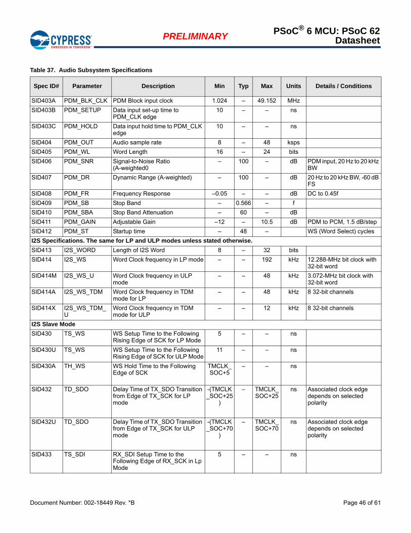
Document Number: 002-18449 Rev. *B Page 46 of 61
PRELIMINARYPSoC® 6 MCU: PSoC 62
Datasheet
SID403A PDM_BLK_CLK PDM Block input clock 1.024 – 49.152 MHz
SID403B PDM_SETUP Data input set-up time to PDM_CLK edge
10 – – ns
SID403C PDM_HOLD Data input hold time to PDM_CLK edge
10 – – ns
SID404 PDM_OUT Audio sample rate 8 – 48 ksps
SID405 PDM_WL Word Length 16 – 24 bits
SID406 PDM_SNR Signal-to-Noise Ratio (A-weighted0
– 100 – dB PDM input, 20 Hz to 20 kHz BW
SID407 PDM_DR Dynamic Range (A-weighted) – 100 – dB 20 Hz to 20 kHz BW, -60 dB FS
SID408 PDM_FR Frequency Response –0.05 – – dB DC to 0.45f
SID409 PDM_SB Stop Band – 0.566 – f
SID410 PDM_SBA Stop Band Attenuation – 60 – dB
SID411 PDM_GAIN Adjustable Gain –12 – 10.5 dB PDM to PCM, 1.5 dB/step
SID412 PDM_ST Startup time – 48 – WS (Word Select) cycles
I2S Specifications. The same for LP and ULP modes unless stated otherwise.
SID413 I2S_WORD Length of I2S Word 8 – 32 bits
SID414 I2S_WS Word Clock frequency in LP mode – – 192 kHz 12.288-MHz bit clock with 32-bit word
SID414M I2S_WS_U Word Clock frequency in ULP mode
– – 48 kHz 3.072-MHz bit clock with 32-bit word
SID414A I2S_WS_TDM Word Clock frequency in TDM mode for LP
– – 48 kHz 8 32-bit channels
SID414X I2S_WS_TDM_U
Word Clock frequency in TDM mode for ULP
– – 12 kHz 8 32-bit channels
I2S Slave Mode
SID430 TS_WS WS Setup Time to the Following Rising Edge of SCK for LP Mode
5 – – ns
SID430U TS_WS WS Setup Time to the Following Rising Edge of SCK for ULP Mode
11 – – ns
SID430A TH_WS WS Hold Time to the Following Edge of SCK
TMCLK_SOC+5
– – ns
SID432 TD_SDO Delay Time of TX_SDO Transition from Edge of TX_SCK for LP mode
-(TMCLK_SOC+25
)
– TMCLK_SOC+25
ns Associated clock edge depends on selected polarity
SID432U TD_SDO Delay Time of TX_SDO Transition from Edge of TX_SCK for ULP mode
-(TMCLK_SOC+70
)
– TMCLK_SOC+70
ns Associated clock edge depends on selected polarity
SID433 TS_SDI RX_SDI Setup Time to the Following Edge of RX_SCK in Lp Mode
5 – – ns
Table 37. Audio Subsystem Specifications
Spec ID# Parameter Description Min Typ Max Units Details / Conditions
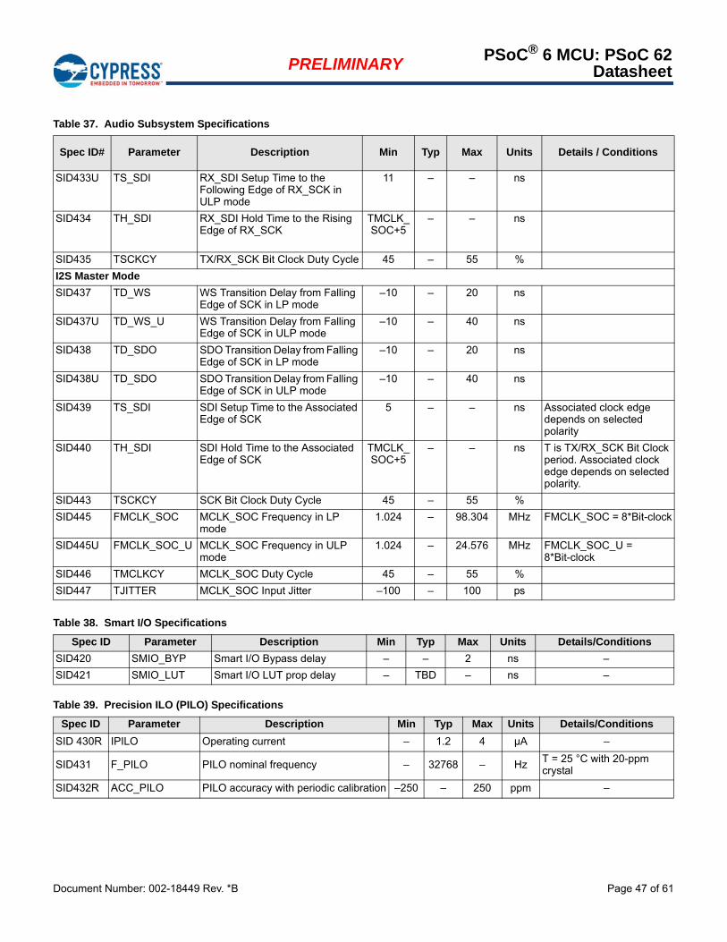
Document Number: 002-18449 Rev. *B Page 47 of 61
PRELIMINARYPSoC® 6 MCU: PSoC 62
Datasheet
SID433U TS_SDI RX_SDI Setup Time to the Following Edge of RX_SCK in ULP mode
11 – – ns
SID434 TH_SDI RX_SDI Hold Time to the Rising Edge of RX_SCK
TMCLK_SOC+5
– – ns
SID435 TSCKCY TX/RX_SCK Bit Clock Duty Cycle 45 – 55 %
I2S Master Mode
SID437 TD_WS WS Transition Delay from Falling Edge of SCK in LP mode
–10 – 20 ns
SID437U TD_WS_U WS Transition Delay from Falling Edge of SCK in ULP mode
–10 – 40 ns
SID438 TD_SDO SDO Transition Delay from Falling Edge of SCK in LP mode
–10 – 20 ns
SID438U TD_SDO SDO Transition Delay from Falling Edge of SCK in ULP mode
–10 – 40 ns
SID439 TS_SDI SDI Setup Time to the Associated Edge of SCK
5 – – ns Associated clock edge depends on selected polarity
SID440 TH_SDI SDI Hold Time to the Associated Edge of SCK
TMCLK_SOC+5
– – ns T is TX/RX_SCK Bit Clock period. Associated clock edge depends on selected polarity.
SID443 TSCKCY SCK Bit Clock Duty Cycle 45 – 55 %
SID445 FMCLK_SOC MCLK_SOC Frequency in LP mode
1.024 – 98.304 MHz FMCLK_SOC = 8*Bit-clock
SID445U FMCLK_SOC_U MCLK_SOC Frequency in ULP mode
1.024 – 24.576 MHz FMCLK_SOC_U = 8*Bit-clock
SID446 TMCLKCY MCLK_SOC Duty Cycle 45 – 55 %
SID447 TJITTER MCLK_SOC Input Jitter –100 – 100 ps
Table 37. Audio Subsystem Specifications
Spec ID# Parameter Description Min Typ Max Units Details / Conditions
Table 38. Smart I/O Specifications
Spec ID Parameter Description Min Typ Max Units Details/Conditions
SID420 SMIO_BYP Smart I/O Bypass delay – – 2 ns –
SID421 SMIO_LUT Smart I/O LUT prop delay – TBD – ns –
Table 39. Precision ILO (PILO) Specifications
Spec ID Parameter Description Min Typ Max Units Details/Conditions
SID 430R IPILO Operating current – 1.2 4 µA –
SID431 F_PILO PILO nominal frequency – 32768 – Hz T = 25 °C with 20-ppm crystal
SID432R ACC_PILO PILO accuracy with periodic calibration –250 – 250 ppm –
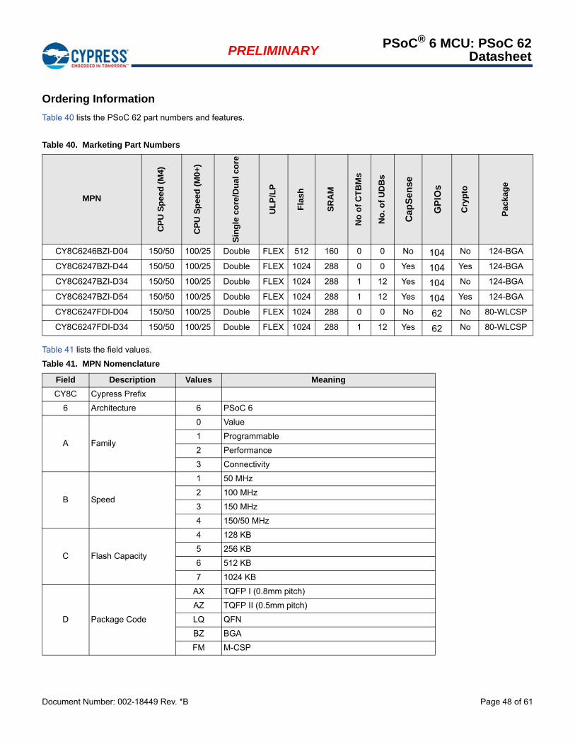
Document Number: 002-18449 Rev. *B Page 48 of 61
PRELIMINARYPSoC® 6 MCU: PSoC 62
Datasheet
Ordering Information
Table 40 lists the PSoC 62 part numbers and features.
Table 41 lists the field values.
Table 40. Marketing Part Numbers
MPN
CP
U S
pee
d (
M4)
CP
U S
pee
d (
M0
+)
Sin
gle
co
re/D
ual
co
re
UL
P/L
P
Fla
sh
SR
AM
No
of
CT
BM
s
No
. of
UD
Bs
Cap
Se
nse
GP
IOs
Cry
pto
Pac
kag
e
CY8C6246BZI-D04 150/50 100/25 Double FLEX 512 160 0 0 No 104 No 124-BGA
CY8C6247BZI-D44 150/50 100/25 Double FLEX 1024 288 0 0 Yes 104 Yes 124-BGA
CY8C6247BZI-D34 150/50 100/25 Double FLEX 1024 288 1 12 Yes 104 No 124-BGA
CY8C6247BZI-D54 150/50 100/25 Double FLEX 1024 288 1 12 Yes 104 Yes 124-BGA
CY8C6247FDI-D04 150/50 100/25 Double FLEX 1024 288 0 0 No 62 No 80-WLCSP
CY8C6247FDI-D34 150/50 100/25 Double FLEX 1024 288 1 12 Yes 62 No 80-WLCSP
Table 41. MPN Nomenclature
Field Description Values Meaning
CY8C Cypress Prefix
6 Architecture 6 PSoC 6
A Family
0 Value
1 Programmable
2 Performance
3 Connectivity
B Speed
1 50 MHz
2 100 MHz
3 150 MHz
4 150/50 MHz
C Flash Capacity
4 128 KB
5 256 KB
6 512 KB
7 1024 KB
D Package Code
AX TQFP I (0.8mm pitch)
AZ TQFP II (0.5mm pitch)
LQ QFN
BZ BGA
FM M-CSP
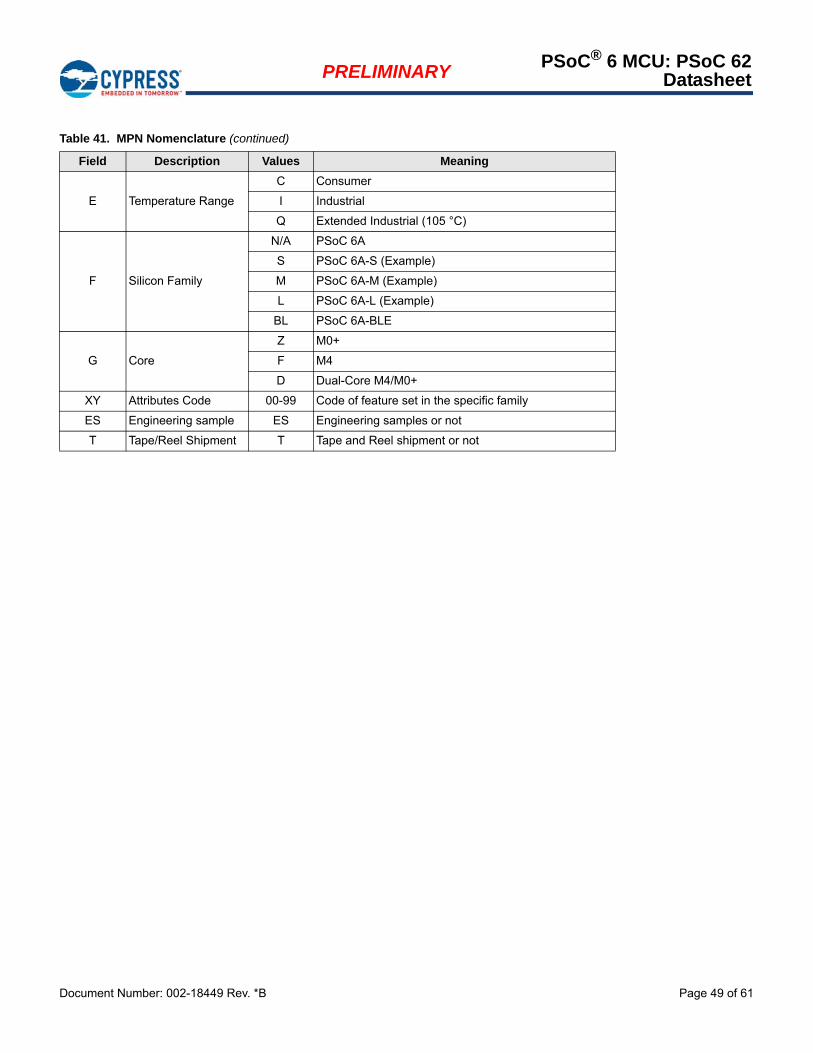
Document Number: 002-18449 Rev. *B Page 49 of 61
PRELIMINARYPSoC® 6 MCU: PSoC 62
Datasheet
E Temperature Range
C Consumer
I Industrial
Q Extended Industrial (105 °C)
F Silicon Family
N/A PSoC 6A
S PSoC 6A-S (Example)
M PSoC 6A-M (Example)
L PSoC 6A-L (Example)
BL PSoC 6A-BLE
G Core
Z M0+
F M4
D Dual-Core M4/M0+
XY Attributes Code 00-99 Code of feature set in the specific family
ES Engineering sample ES Engineering samples or not
T Tape/Reel Shipment T Tape and Reel shipment or not
Table 41. MPN Nomenclature (continued)
Field Description Values Meaning
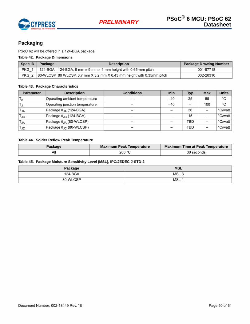
Document Number: 002-18449 Rev. *B Page 50 of 61
PRELIMINARYPSoC® 6 MCU: PSoC 62
Datasheet
Packaging
PSoC 62 will be offered in a 124-BGA package.
Table 42. Package Dimensions
Spec ID Package Description Package Drawing Number
PKG_1 124-BGA 124-BGA, 9 mm 9 mm 1 mm height with 0.65-mm pitch 001-97718
PKG_2 80-WLCSP 80 WLCSP, 3.7 mm X 3.2 mm X 0.43 mm height with 0.35mm pitch 002-20310
Table 43. Package Characteristics
Parameter Description Conditions Min Typ Max Units
TA Operating ambient temperature – –40 25 85 °C
TJ Operating junction temperature – –40 – 100 °C
TJA Package JA (124-BGA) – – 36 – °C/watt
TJC Package JC (124-BGA) – – 15 – °C/watt
TJA Package JA (80-WLCSP) – – TBD – °C/watt
TJC Package JC (80-WLCSP) – – TBD – °C/watt
Table 44. Solder Reflow Peak Temperature
Package Maximum Peak Temperature Maximum Time at Peak Temperature
All 260 °C 30 seconds
Table 45. Package Moisture Sensitivity Level (MSL), IPC/JEDEC J-STD-2
Package MSL
124-BGA MSL 3
80-WLCSP MSL 1
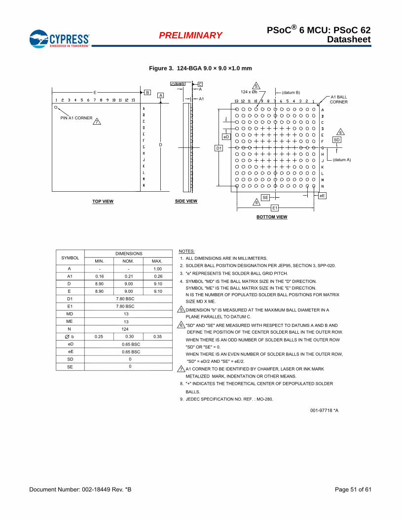
Document Number: 002-18449 Rev. *B Page 51 of 61
PRELIMINARYPSoC® 6 MCU: PSoC 62
Datasheet
Figure 3. 124-BGA 9.0 × 9.0 ×1.0 mm
SD
b
eE
eD
ME
N
0.25
0
0.65 BSC
0.65 BSC
0.30
124
13
0.35
DIMENSIONS
D1
MD
E1
E
D
A
A1
SYMBOL
0.16
MIN.
-
7.80 BSC
7.80 BSC
13
9.00
NOM.
- 1.00
MAX.
SE 0
9.00
9.10
9.10
8.90
8.90
0.21 0.26
N IS THE NUMBER OF POPULATED SOLDER BALL POSITIONS FOR MATRIX
WHEN THERE IS AN EVEN NUMBER OF SOLDER BALLS IN THE OUTER ROW,
WHEN THERE IS AN ODD NUMBER OF SOLDER BALLS IN THE OUTER ROW
DEFINE THE POSITION OF THE CENTER SOLDER BALL IN THE OUTER ROW. "SD" AND "SE" ARE MEASURED WITH RESPECT TO DATUMS A AND B AND
SYMBOL "ME" IS THE BALL MATRIX SIZE IN THE "E" DIRECTION. SYMBOL "MD" IS THE BALL MATRIX SIZE IN THE "D" DIRECTION.
"e" REPRESENTS THE SOLDER BALL GRID PITCH.
DIMENSION "b" IS MEASURED AT THE MAXIMUM BALL DIAMETER IN A
SOLDER BALL POSITION DESIGNATION PER JEP95, SECTION 3, SPP-020.
"+" INDICATES THE THEORETICAL CENTER OF DEPOPULATED SOLDER
A1 CORNER TO BE IDENTIFIED BY CHAMFER, LASER OR INK MARK
8.
7.
6.
NOTES:
5.
4.
3.
2.
1. ALL DIMENSIONS ARE IN MILLIMETERS.
METALIZED MARK, INDENTATION OR OTHER MEANS.
"SD" = eD/2 AND "SE" = eE/2.
PLANE PARALLEL TO DATUM C.
"SD" OR "SE" = 0.
SIZE MD X ME.
BALLS.
JEDEC SPECIFICATION NO. REF. : MO-280.9.
PIN A1 CORNER
SIDE VIEW
BOTTOM VIEW
TOP VIEW
A1 BALLCORNER
124 x Øb E
D
A
A1
eE
eD
D1
E1
(datum B)
(datum A)
5.
SD
6
SE6
7.
BA
C
001-97718 *A
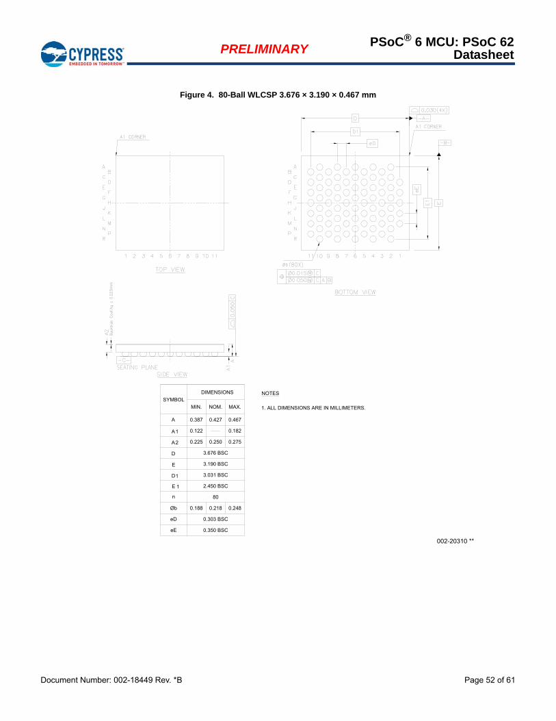
Document Number: 002-18449 Rev. *B Page 52 of 61
PRELIMINARYPSoC® 6 MCU: PSoC 62
Datasheet
Figure 4. 80-Ball WLCSP 3.676 × 3.190 × 0.467 mm
DIMENSIONS
NOM.MIN.
3.031 BSCD1
E 1
E
2.450 BSC
3.190 BSC
D
A
1A
3.676 BSC
0.122
SYMBOLMAX.
0.467
0.182
1. ALL DIMENSIONS ARE IN MILLIMETERS.
Øb
eE
eD
80
0.188 0.2480.218
0.303 BSC
0.350 BSC
n
NOTES
0.4270.387
2A 0.225 0.2750.250
002-20310 **
Document Number: 002-18449 Rev. *B Page 53 of 61
PRELIMINARYPSoC® 6 MCU: PSoC 62
Datasheet
Acronyms
Table 46. Acronyms Used in this Document
Acronym Description
abus analog local bus
ADC analog-to-digital converter
AG analog global
AHBAMBA (advanced microcontroller bus archi-tecture) high-performance bus, an ARM data transfer bus
ALU arithmetic logic unit
AMUXBUS analog multiplexer bus
API application programming interface
APSR application program status register
ARM® advanced RISC machine, a CPU architecture
ATM automatic thump mode
BW bandwidth
CANController Area Network, a communications protocol
CMRR common-mode rejection ratio
CPU central processing unit
CRC cyclic redundancy check, an error-checking protocol
DAC digital-to-analog converter, see also IDAC, VDAC
DFB digital filter block
DIO digital input/output, GPIO with only digital capabilities, no analog. See GPIO.
DMIPS Dhrystone million instructions per second
DMA direct memory access, see also TD
DNL differential nonlinearity, see also INL
DNU do not use
DR port write data registers
DSI digital system interconnect
DWT data watchpoint and trace
ECC error correcting code
ECO external crystal oscillator
EEPROMelectrically erasable programmable read-only memory
EMI electromagnetic interference
EMIF external memory interface
EOC end of conversion
EOF end of frame
EPSR execution program status register
ESD electrostatic discharge
ETM embedded trace macrocell
FIR finite impulse response, see also IIR
FPB flash patch and breakpoint
FS full-speed
GPIO general-purpose input/output, applies to a PSoC pin
HVI high-voltage interrupt, see also LVI, LVD
IC integrated circuit
IDAC current DAC, see also DAC, VDAC
IDE integrated development environment
I2C, or IICInter-Integrated Circuit, a communications protocol
IIR infinite impulse response, see also FIR
ILO internal low-speed oscillator, see also IMO
IMO internal main oscillator, see also ILO
INL integral nonlinearity, see also DNL
I/O input/output, see also GPIO, DIO, SIO, USBIO
IPOR initial power-on reset
IPSR interrupt program status register
IRQ interrupt request
ITM instrumentation trace macrocell
LCD liquid crystal display
LIN Local Interconnect Network, a communications protocol.
LR link register
LUT lookup table
LVD low-voltage detect, see also LVI
LVI low-voltage interrupt, see also HVI
LVTTL low-voltage transistor-transistor logic
MAC multiply-accumulate
MCU microcontroller unit
MISO master-in slave-out
NC no connect
NMI nonmaskable interrupt
NRZ non-return-to-zero
NVIC nested vectored interrupt controller
NVL nonvolatile latch, see also WOL
opamp operational amplifier
PAL programmable array logic, see also PLD
PC program counter
Table 46. Acronyms Used in this Document (continued)
Acronym Description
Document Number: 002-18449 Rev. *B Page 54 of 61
PRELIMINARYPSoC® 6 MCU: PSoC 62
Datasheet
PCB printed circuit board
PGA programmable gain amplifier
PHUB peripheral hub
PHY physical layer
PICU port interrupt control unit
PLA programmable logic array
PLD programmable logic device, see also PAL
PLL phase-locked loop
PMDD package material declaration data sheet
POR power-on reset
PRES precise power-on reset
PRS pseudo random sequence
PS port read data register
PSoC® Programmable System-on-Chip™
PSRR power supply rejection ratio
PWM pulse-width modulator
RAM random-access memory
RISC reduced-instruction-set computing
RMS root-mean-square
RTC real-time clock
RTL register transfer language
RTR remote transmission request
RX receive
SAR successive approximation register
SC/CT switched capacitor/continuous time
SCL I2C serial clock
SDA I2C serial data
S/H sample and hold
SINAD signal to noise and distortion ratio
SIOspecial input/output, GPIO with advanced features. See GPIO.
SOC start of conversion
SOF start of frame
SPI Serial Peripheral Interface, a communications protocol
SR slew rate
SRAM static random access memory
SRES software reset
SWD serial wire debug, a test protocol
SWV single-wire viewer
Table 46. Acronyms Used in this Document (continued)
Acronym Description
TD transaction descriptor, see also DMA
THD total harmonic distortion
TIA transimpedance amplifier
TRM technical reference manual
TTL transistor-transistor logic
TX transmit
UARTUniversal Asynchronous Transmitter Receiver, a communications protocol
UDB universal digital block
USB Universal Serial Bus
USBIO USB input/output, PSoC pins used to connect to a USB port
VDAC voltage DAC, see also DAC, IDAC
WDT watchdog timer
WOL write once latch, see also NVL
WRES watchdog timer reset
XRES external reset I/O pin
XTAL crystal
Table 46. Acronyms Used in this Document (continued)
Acronym Description
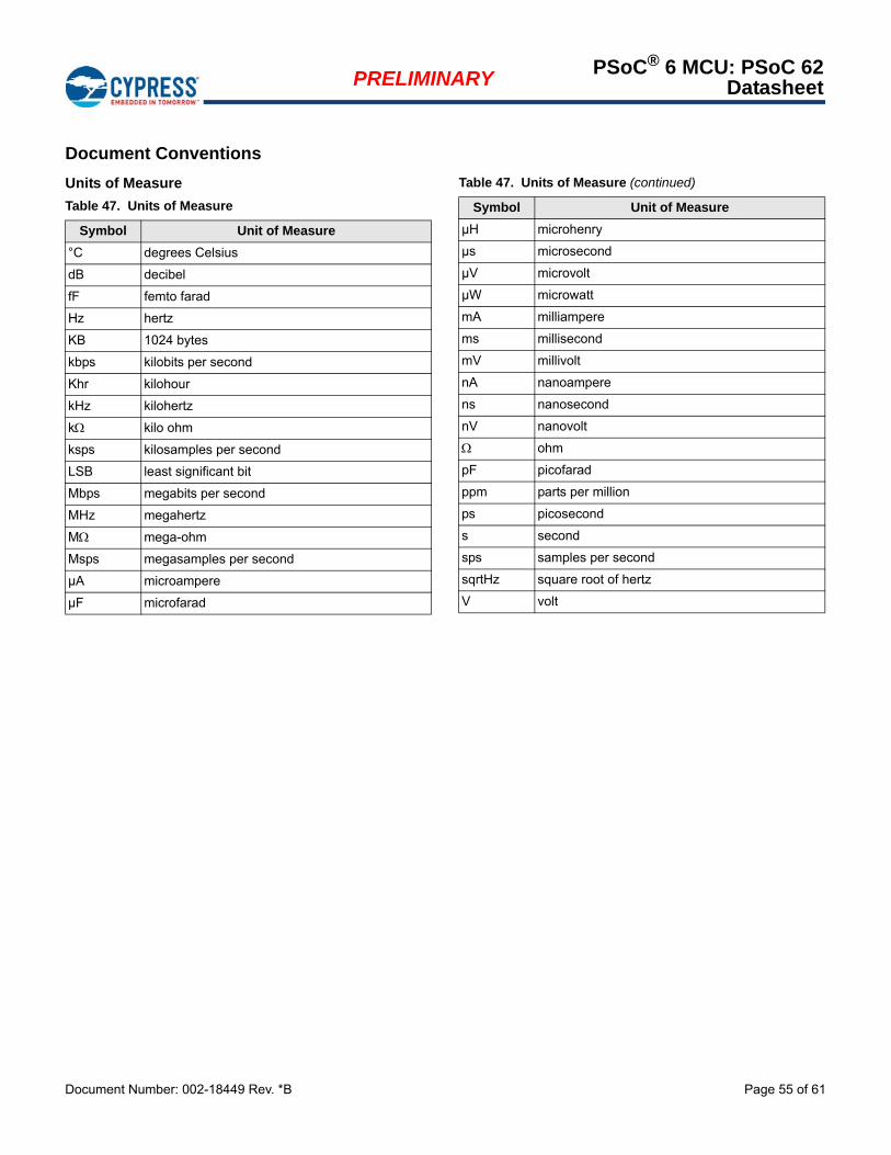
Document Number: 002-18449 Rev. *B Page 55 of 61
PRELIMINARYPSoC® 6 MCU: PSoC 62
Datasheet
Document Conventions
Units of Measure
Table 47. Units of Measure
Symbol Unit of Measure
°C degrees Celsius
dB decibel
fF femto farad
Hz hertz
KB 1024 bytes
kbps kilobits per second
Khr kilohour
kHz kilohertz
k kilo ohm
ksps kilosamples per second
LSB least significant bit
Mbps megabits per second
MHz megahertz
M mega-ohm
Msps megasamples per second
µA microampere
µF microfarad
µH microhenry
µs microsecond
µV microvolt
µW microwatt
mA milliampere
ms millisecond
mV millivolt
nA nanoampere
ns nanosecond
nV nanovolt
ohm
pF picofarad
ppm parts per million
ps picosecond
s second
sps samples per second
sqrtHz square root of hertz
V volt
Table 47. Units of Measure (continued)
Symbol Unit of Measure
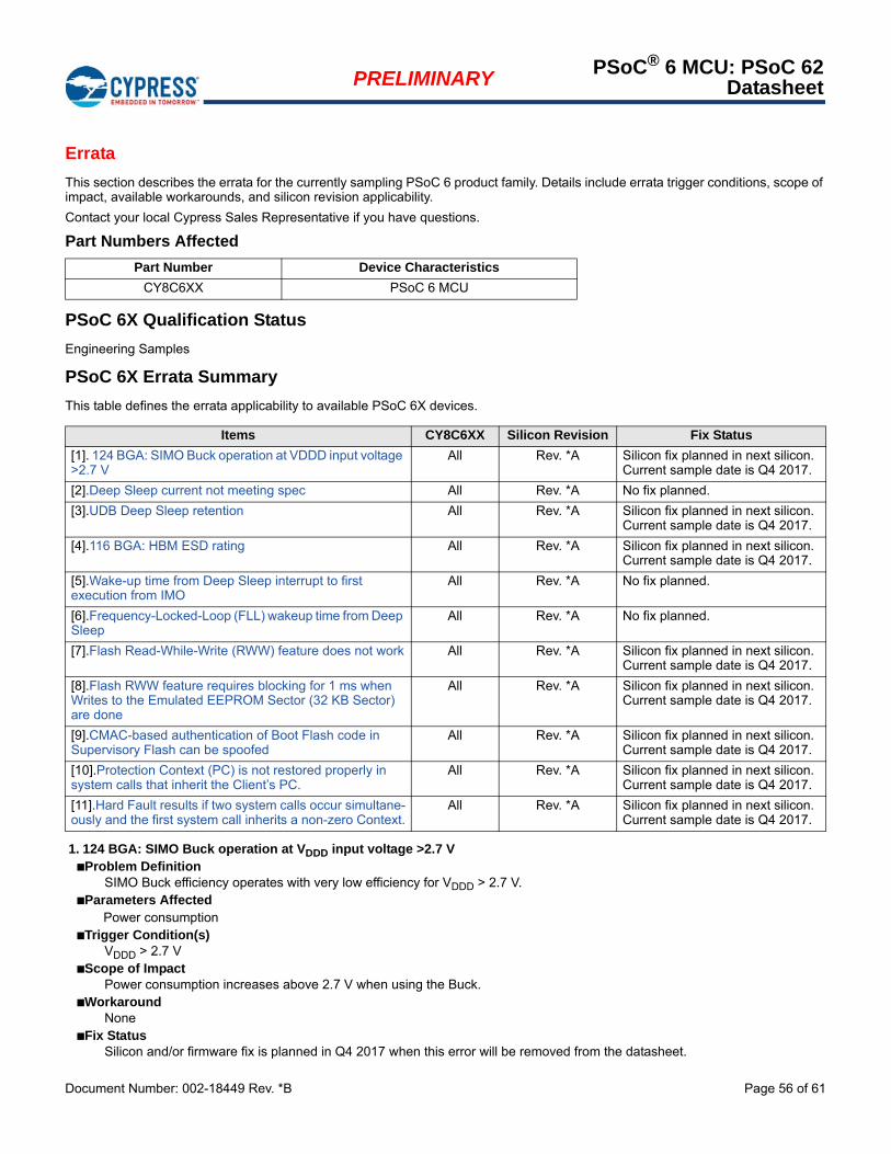
Document Number: 002-18449 Rev. *B Page 56 of 61
PRELIMINARYPSoC® 6 MCU: PSoC 62
Datasheet
Errata
This section describes the errata for the currently sampling PSoC 6 product family. Details include errata trigger conditions, scope of impact, available workarounds, and silicon revision applicability.
Contact your local Cypress Sales Representative if you have questions.
Part Numbers Affected
PSoC 6X Qualification Status
Engineering Samples
PSoC 6X Errata Summary
This table defines the errata applicability to available PSoC 6X devices.
1. 124 BGA: SIMO Buck operation at VDDD input voltage >2.7 VProblem Definition
SIMO Buck efficiency operates with very low efficiency for VDDD > 2.7 V.Parameters Affected
Power consumptionTrigger Condition(s)
VDDD > 2.7 VScope of Impact
Power consumption increases above 2.7 V when using the Buck.Workaround
NoneFix Status
Silicon and/or firmware fix is planned in Q4 2017 when this error will be removed from the datasheet.
Part Number Device Characteristics
CY8C6XX PSoC 6 MCU
Items CY8C6XX Silicon Revision Fix Status
[1]. 124 BGA: SIMO Buck operation at VDDD input voltage >2.7 V
All Rev. *A Silicon fix planned in next silicon. Current sample date is Q4 2017.
[2].Deep Sleep current not meeting spec All Rev. *A No fix planned.
[3].UDB Deep Sleep retention All Rev. *A Silicon fix planned in next silicon. Current sample date is Q4 2017.
[4].116 BGA: HBM ESD rating All Rev. *A Silicon fix planned in next silicon. Current sample date is Q4 2017.
[5].Wake-up time from Deep Sleep interrupt to first execution from IMO
All Rev. *A No fix planned.
[6].Frequency-Locked-Loop (FLL) wakeup time from Deep Sleep
All Rev. *A No fix planned.
[7].Flash Read-While-Write (RWW) feature does not work All Rev. *A Silicon fix planned in next silicon. Current sample date is Q4 2017.
[8].Flash RWW feature requires blocking for 1 ms when Writes to the Emulated EEPROM Sector (32 KB Sector) are done
All Rev. *A Silicon fix planned in next silicon. Current sample date is Q4 2017.
[9].CMAC-based authentication of Boot Flash code in Supervisory Flash can be spoofed
All Rev. *A Silicon fix planned in next silicon. Current sample date is Q4 2017.
[10].Protection Context (PC) is not restored properly in system calls that inherit the Client’s PC.
All Rev. *A Silicon fix planned in next silicon. Current sample date is Q4 2017.
[11].Hard Fault results if two system calls occur simultane-ously and the first system call inherits a non-zero Context.
All Rev. *A Silicon fix planned in next silicon. Current sample date is Q4 2017.
Document Number: 002-18449 Rev. *B Page 57 of 61
PRELIMINARYPSoC® 6 MCU: PSoC 62
Datasheet
2. Deep Sleep current not meeting specProblem Definition
Deep Sleep current does not meet the spec; it is 7 µA versus spec of 4.5 µA (64-KB SRAM retained) and 9 µA vs spec of 7 µA(256-KB SRAM retained).]
Parameters AffectedDeep Sleep current
Trigger Condition(s)NA
Scope of ImpactDeep Sleep current budget will be higher
WorkaroundNone
Fix StatusNo fix is planned
3. UDB Deep Sleep retentionProblem Definition
GPIOs driven from the UDB circuit may fail to maintain state after wakeup from Deep Sleep.Parameters Affected
GPIO states if driven by UDBsTrigger Condition(s)
NAScope of Impact
Erroneous logic states may occur transiently for outputs controlled by UDB logic after wakeup from Deep Sleep.Workaround
NoneFix Status
Silicon and/or firmware fix is planned in Q4 2017 when this error will be removed from the datasheet.
4. 116 BGA: HBM ESD ratingProblem Definition
HBM ESD is rated at 1600 V versus spec of 2200 V on the 116 BGA package.Parameters Affected
HBM ESD rating on the 116 BGA packageTrigger Condition(s)
NAScope of Impact
HBM spec of 2000 V not met for the 116 BGA packageWorkaround
NoneFix Status
Silicon and/or firmware fix is planned in Q4 2017 when this error is expected to be removed from the datasheet
5. Wake-up time from Deep Sleep interrupt to first execution from IMOProblem Definition
Wakeup time from Deep Sleep interrupt to firmware execution is 21 µs instead of 11 µs.Parameters Affected
Time from Deep Sleep wakeup to firmware executionTrigger Condition(s)
NAScope of Impact
Longer Deep Sleep wakeup time
Document Number: 002-18449 Rev. *B Page 58 of 61
PRELIMINARYPSoC® 6 MCU: PSoC 62
Datasheet
WorkaroundNone
Fix Status
No fix planned
6. Frequency-Locked-Loop (FLL) wakeup time from Deep SleepProblem Definition
Time from Deep Sleep wakeup to execution from FLL is 26 µs instead of 15 µs.Parameters Affected
Time from Deep Sleep wakeup to firmware execution from FLLTrigger Condition(s)
NAScope of Impact
Longer Deep Sleep wakeup time to firmware execution from FLLWorkaround
NoneFix Status
No fix planned
7. Flash Read-While-Write (RWW) feature does not workProblem Definition
Reading from one Flash Sector while writing to another is non-functional.Parameters Affected
NATrigger Condition(s)
Attempting to read from a Flash address while Flash is being written to.Scope of Impact
Attempting to use the RWW feature will cause Hard Faults.Workaround
Use Blocking calls for System API functions. DMA/Data-Wire, Crypto, and SMIF (QSPI) blocks are bus masters and must bedisabled while the Blocking call is underway if they make any Flash accesses. Basically, there must be no Flash access beforethe Blocking call is completed. There is a partial workaround for a special case described in the next item.
Fix Status
Silicon and/or firmware fix is planned in Q4 2017 when this error will be removed from the datasheet.
8. Flash RWW feature requires blocking for 1 ms when Writes to the Emulated EEPROM Sector (32 KB Sector) are doneProblem Definition
Writing to the 32-KB Flash Sector while attempting to read Flash before 1 ms from the beginning of the Write does not work.Parameters Affected
NATrigger Condition(s)
Attempting to read from a Flash address less than 1 ms after the beginning of a write to the 32-KB Flash sector.Scope of Impact
Attempting to read from Flash less than 1 ms after the beginning of a write to the 32-KB sector will cause Hard Faults.Workaround
DMA/Data-Wire, Crypto, and SMIF (QSPI) blocks are bus masters and must be disabled for a period of 1 ms after the call ismade if they access Flash. Basically, there must be no Flash access for a period of 1 ms after a write to the 32-KB Sector isinitiated. This workaround allows BLE connectivity to be maintained when the 32-KB sector is used for writing pairing informa-tion.
Fix Status
Silicon and/or firmware fix is planned in Q4 2017 when this error will be removed from the datasheet.
Document Number: 002-18449 Rev. *B Page 59 of 61
PRELIMINARYPSoC® 6 MCU: PSoC 62
Datasheet
9. CMAC-based authentication of Boot Flash code in Supervisory Flash can be spoofedProblem Definition
CMAC is used to verify authenticity of the Boot Flash but the AES key can be made visible and the integrity of the MessageAuthentication is compromised.
Parameters AffectedNA
Trigger Condition(s)NA
Scope of ImpactThe AES Key is stored in SROM and can be read out in parts, which are in the normal life cycle stage mode. This will bereplaced by a Secure Hash Authentication (SHA) method, which does not use a key.
WorkaroundNone
Fix Status
Silicon and/or firmware fix is planned in Q4 2017 when this error will be removed from the datasheet.
10.Protection Context (PC) is not restored properly in system calls that inherit the Client’s PC. Problem Definition
Some System calls can inherit the client's Protection Context (PC); the PC is restored on completion of the call except for theinheritance of PC 0.
Parameters AffectedNA
Trigger Condition(s)NA
Scope of ImpactProtection context can be changed inadvertently causing access failures.
WorkaroundFor System Calls that inherit the Client's Protection Context (PC), PC_SAVED must be Set to 0 if the previous ProtectionContext was PC0. The CM0+ must be used in Protection Context 0.
Fix Status
Silicon and/or firmware fix is planned in Q4 2017 when this error will be removed from the datasheet.
11.Hard Fault results if two system calls occur simultaneously and the first system call inherits a non-zero Context. Problem Definition
If two system calls are made simultaneously, the NMI Handler will try to service the second system call as well before returning.If the first system call inherited a non-zero Protection Context, then the second call will cause a Hard Fault if tries to access aprotected region.
Parameters AffectedNA
Trigger Condition(s)Back-to-back system calls with the first call inheriting a non-zero Protection Context.
Scope of ImpactProtection context can be changed inadvertently causing access failures.
WorkaroundWorkaround is to use an IPC channel to make sure that the first system call is completed before making the next call.
Fix Status
Silicon and/or firmware fix is planned in Q4 2017 when this error will be removed from the datasheet.
Document Number: 002-18449 Rev. *B Page 60 of 61
PRELIMINARYPSoC® 6 MCU: PSoC 62
Datasheet
Revision History
Description Title: PSoC® 6 MCU: PSoC 62 Datasheet, Programmable System-on-Chip (PSoC®)Document Number: 002-18449
Revision ECN Orig. of Change
Submission Date Description of Change
*B 5896512 WKA 09/26/2017 Released to web for PSoC 62.
Document Number: 002-18449 Rev. *B Revised September 26, 2017 Page 61 of 61
PRELIMINARYPSoC® 6 MCU: PSoC 62
Datasheet
© Cypress Semiconductor Corporation, 2017. This document is the property of Cypress Semiconductor Corporation and its subsidiaries, including Spansion LLC ("Cypress"). This document, includingany software or firmware included or referenced in this document ("Software"), is owned by Cypress under the intellectual property laws and treaties of the United States and other countries worldwide.Cypress reserves all rights under such laws and treaties and does not, except as specifically stated in this paragraph, grant any license under its patents, copyrights, trademarks, or other intellectualproperty rights. If the Software is not accompanied by a license agreement and you do not otherwise have a written agreement with Cypress governing the use of the Software, then Cypress herebygrants you a personal, non-exclusive, nontransferable license (without the right to sublicense) (1) under its copyright rights in the Software (a) for Software provided in source code form, to modify andreproduce the Software solely for use with Cypress hardware products, only internally within your organization, and (b) to distribute the Software in binary code form externally to end users (eitherdirectly or indirectly through resellers and distributors), solely for use on Cypress hardware product units, and (2) under those claims of Cypress's patents that are infringed by the Software (as providedby Cypress, unmodified) to make, use, distribute, and import the Software solely for use with Cypress hardware products. Any other use, reproduction, modification, translation, or compilation of theSoftware is prohibited.
TO THE EXTENT PERMITTED BY APPLICABLE LAW, CYPRESS MAKES NO WARRANTY OF ANY KIND, EXPRESS OR IMPLIED, WITH REGARD TO THIS DOCUMENT OR ANY SOFTWAREOR ACCOMPANYING HARDWARE, INCLUDING, BUT NOT LIMITED TO, THE IMPLIED WARRANTIES OF MERCHANTABILITY AND FITNESS FOR A PARTICULAR PURPOSE. To the extentpermitted by applicable law, Cypress reserves the right to make changes to this document without further notice. Cypress does not assume any liability arising out of the application or use of anyproduct or circuit described in this document. Any information provided in this document, including any sample design information or programming code, is provided only for reference purposes. It isthe responsibility of the user of this document to properly design, program, and test the functionality and safety of any application made of this information and any resulting product. Cypress productsare not designed, intended, or authorized for use as critical components in systems designed or intended for the operation of weapons, weapons systems, nuclear installations, life-support devices orsystems, other medical devices or systems (including resuscitation equipment and surgical implants), pollution control or hazardous substances management, or other uses where the failure of thedevice or system could cause personal injury, death, or property damage ("Unintended Uses"). A critical component is any component of a device or system whose failure to perform can be reasonablyexpected to cause the failure of the device or system, or to affect its safety or effectiveness. Cypress is not liable, in whole or in part, and you shall and hereby do release Cypress from any claim,damage, or other liability arising from or related to all Unintended Uses of Cypress products. You shall indemnify and hold Cypress harmless from and against all claims, costs, damages, and otherliabilities, including claims for personal injury or death, arising from or related to any Unintended Uses of Cypress products.
Cypress, the Cypress logo, Spansion, the Spansion logo, and combinations thereof, WICED, PSoC, CapSense, EZ-USB, F-RAM, and Traveo are trademarks or registered trademarks of Cypress inthe United States and other countries. For a more complete list of Cypress trademarks, visit cypress.com. Other names and brands may be claimed as property of their respective owners.
Sales, Solutions, and Legal Information
Worldwide Sales and Design Support
Cypress maintains a worldwide network of offices, solution centers, manufacturer’s representatives, and distributors. To find the office closest to you, visit us at Cypress Locations.
Products
ARM® Cortex® Microcontrollers cypress.com/arm
Automotive cypress.com/automotive
Clocks & Buffers cypress.com/clocks
Interface cypress.com/interface
Internet of Things cypress.com/iot
Memory cypress.com/memory
Microcontrollers cypress.com/mcu
PSoC cypress.com/psoc
Power Management ICs cypress.com/pmic
Touch Sensing cypress.com/touch
USB Controllers cypress.com/usb
Wireless Connectivity cypress.com/wireless
PSoC® Solutions
PSoC 1 | PSoC 3 | PSoC 4 | PSoC 5LP | PSoC 6
Cypress Developer Community
Forums | WICED IOT Forums | Projects | Video | Blogs | Training | Components
Technical Support
cypress.com/support