Embed Size (px)
Citation preview
Project Report: Band Structure of GaAs usingk.p-theory
Austin IrishMikael Thorstrom
December 12th 2017
1 Introduction
The objective of the project was to calculate the band structure of both strainedand unstrained Gallium arsenide, GaAs, using the standard model. The strainedband structure is useful to calculate since the bands will change with the materialbeing sandwiched with different lattice materials. To calculate this the 8-band k · ptheory will be used, which will give a fairly accurate result for small k-values.
2 Theory
Solving the Schrodinger equation for electrons in a crystalline solid reveals the elec-tronic states and energy levels, Eq.1, where p = −ih∇ is the momentum operator,m0 is electron rest mass, V (r) is the periodic position dependent potential in thematerial, ψ is the electron wave function and E is the energy.[ p2
2m0
+ V (r)]ψ = Eψ (1)
This is quite useful for studying the electronic properties of bulk homogeneoussemiconductors, however heterostructures and quantum structures complicate solv-ing Eq.1 and approximation methods must be used. k · p perturbation theory is oneof the methods for solving for the electronic and optical properties of these morecomplicated crystalline solids. Davies in (7) describes how with Bloch functions andthe k · p method we can write the wave function as
Ψn,k(r) = eik·run,k(r)
Using these Bloch functions as solutions to the Schrodinger equation, we get
Hkun,k = En,kun,k
where the Hamiltonian, H, becomes (note the k · p operator):
1
Hk =p2
2m0
+hk · pm0
+h2k2
2m0
+ V
with components dependent on and independent of k. The Hamiltonian at k=0reduces to H0 and we are left with Eq. 2, as described by Cardona and Pollak (6).
H0ψ =[ p2
2m0
+ V]ψ = Eψ (2)
Though technically not necessary, solving the Schrodinger equation only in the Bril-louin zone center where k ≈ 0, greatly simplifies things. The so called 8-band k · ptheory does this for eight (four spin up/down degenerate) energy levels, the firstconduction band and the first three valence bands: heavy holes, light holes and thesplit-off band.
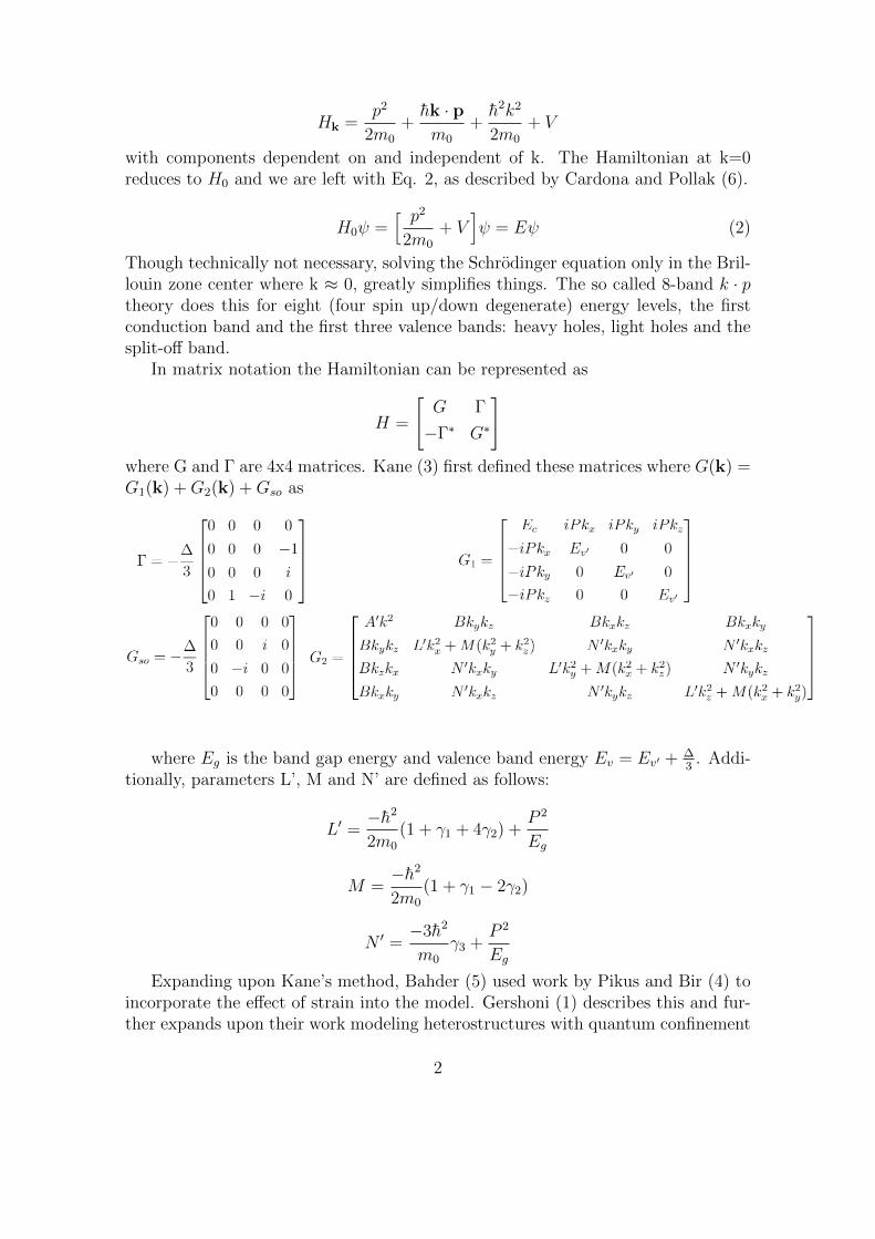
In matrix notation the Hamiltonian can be represented as
H =
[G Γ
−Γ∗ G∗
]where G and Γ are 4x4 matrices. Kane (3) first defined these matrices where G(k) =G1(k) +G2(k) +Gso as
where Eg is the band gap energy and valence band energy Ev = Ev′ + ∆3
. Addi-tionally, parameters L’, M and N’ are defined as follows:
L′ =−h2
2m0
(1 + γ1 + 4γ2) +P 2
Eg
M =−h2
2m0
(1 + γ1 − 2γ2)
N ′ =−3h2
m0
γ3 +P 2
Eg
Expanding upon Kane’s method, Bahder (5) used work by Pikus and Bir (4) toincorporate the effect of strain into the model. Gershoni (1) describes this and fur-ther expands upon their work modeling heterostructures with quantum confinement
2
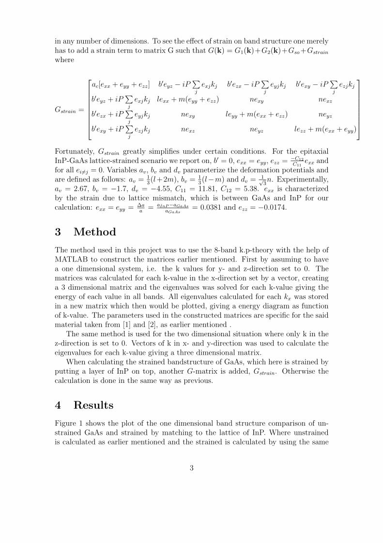
in any number of dimensions. To see the effect of strain on band structure one merelyhas to add a strain term to matrix G such that G(k) = G1(k)+G2(k)+Gso+Gstrain
where
Gstrain =
ac[exx + eyy + ezz] b′eyz − iP∑j
exjkj b′ezx − iP∑j
eyjkj b′exy − iP∑j
ezjkj
b′eyz + iP∑j
exjkj lexx +m(eyy + ezz) nexy nexz
b′ezx + iP∑j
eyjkj nexy leyy +m(exx + ezz) neyz
b′exy + iP∑j
ezjkj nexz neyz lezz +m(exx + eyy)
Fortunately, Gstrain greatly simplifies under certain conditions. For the epitaxialInP-GaAs lattice-strained scenario we report on, b′ = 0, exx = eyy, ezz = −C12
C11exx and
for all ei 6=j = 0. Variables av, bv and dv parameterize the deformation potentials andare defined as follows: av = 1
3(l+2m), bv = 1
3(l−m) and dv = 1√
3n. Experimentally,
av = 2.67, bv = −1.7, dv = −4.55, C11 = 11.81, C12 = 5.38. exx is characterizedby the strain due to lattice mismatch, which is between GaAs and InP for ourcalculation: exx = eyy = ∆a
a= aInP−aGaAs
aGaAs= 0.0381 and ezz = −0.0174.
3 Method
The method used in this project was to use the 8-band k.p-theory with the help ofMATLAB to construct the matrices earlier mentioned. First by assuming to havea one dimensional system, i.e. the k values for y- and z-direction set to 0. Thematrices was calculated for each k-value in the x-direction set by a vector, creatinga 3 dimensional matrix and the eigenvalues was solved for each k-value giving theenergy of each value in all bands. All eigenvalues calculated for each kx was storedin a new matrix which then would be plotted, giving a energy diagram as functionof k-value. The parameters used in the constructed matrices are specific for the saidmaterial taken from [1] and [2], as earlier mentioned .
The same method is used for the two dimensional situation where only k in thez-direction is set to 0. Vectors of k in x- and y-direction was used to calculate theeigenvalues for each k-value giving a three dimensional matrix.
When calculating the strained bandstructure of GaAs, which here is strained byputting a layer of InP on top, another G-matrix is added, Gstrain. Otherwise thecalculation is done in the same way as previous.
4 Results
Figure 1 shows the plot of the one dimensional band structure comparison of un-strained GaAs and strained by matching to the lattice of InP. Where unstrainedis calculated as earlier mentioned and the strained is calculated by using the same
3
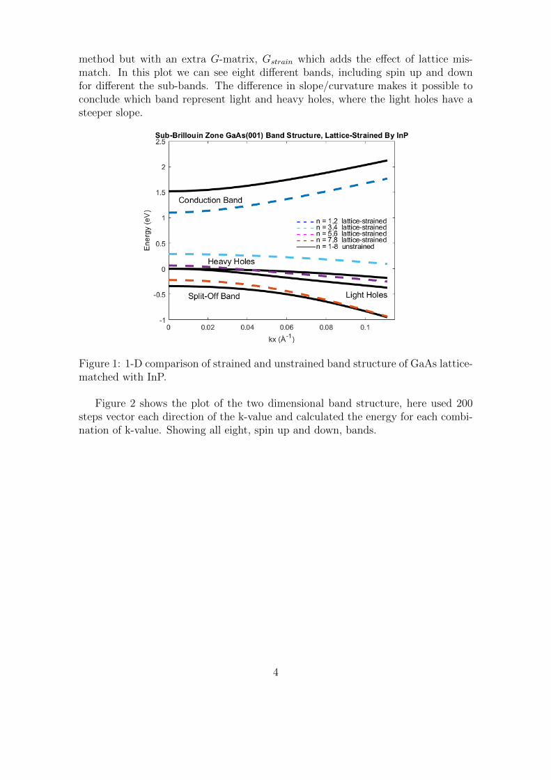
method but with an extra G-matrix, Gstrain which adds the effect of lattice mis-match. In this plot we can see eight different bands, including spin up and downfor different the sub-bands. The difference in slope/curvature makes it possible toconclude which band represent light and heavy holes, where the light holes have asteeper slope.
Figure 1: 1-D comparison of strained and unstrained band structure of GaAs lattice-matched with InP.
Figure 2 shows the plot of the two dimensional band structure, here used 200steps vector each direction of the k-value and calculated the energy for each combi-nation of k-value. Showing all eight, spin up and down, bands.
4
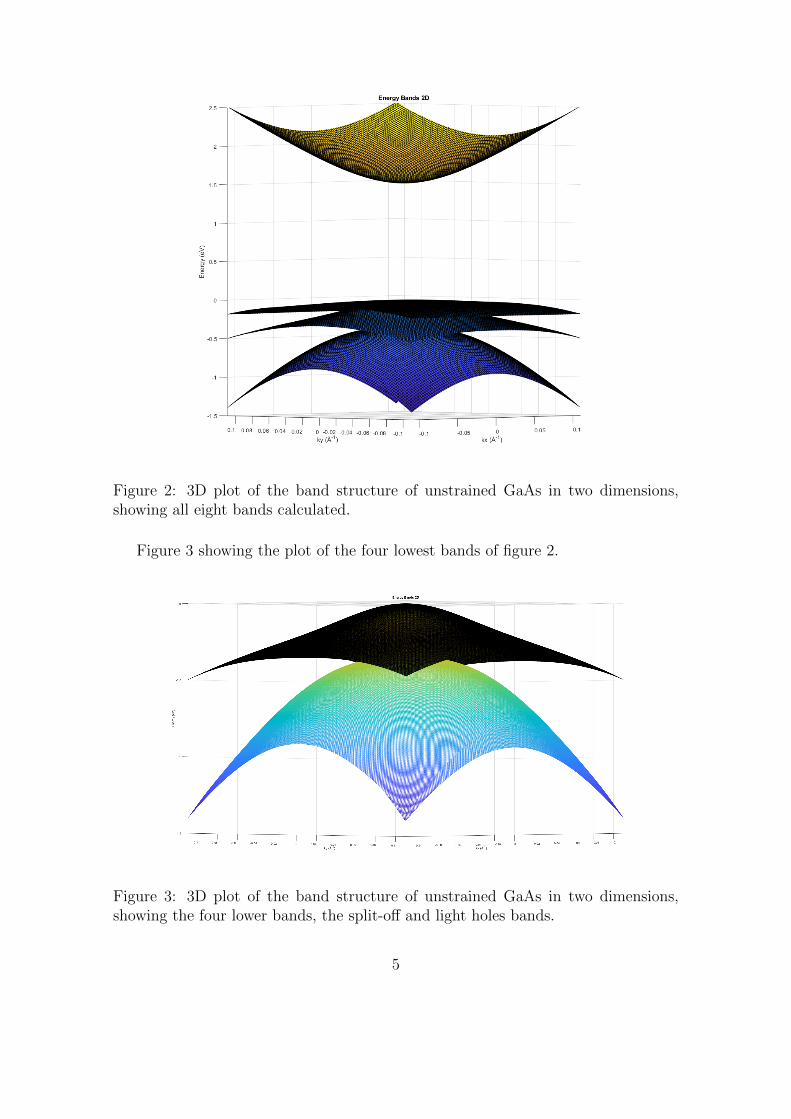
Figure 2: 3D plot of the band structure of unstrained GaAs in two dimensions,showing all eight bands calculated.
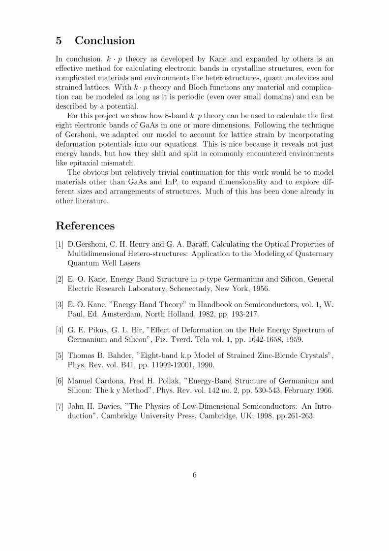
Figure 3 showing the plot of the four lowest bands of figure 2.
Figure 3: 3D plot of the band structure of unstrained GaAs in two dimensions,showing the four lower bands, the split-off and light holes bands.
5
5 Conclusion
In conclusion, k · p theory as developed by Kane and expanded by others is aneffective method for calculating electronic bands in crystalline structures, even forcomplicated materials and environments like heterostructures, quantum devices andstrained lattices. With k · p theory and Bloch functions any material and complica-tion can be modeled as long as it is periodic (even over small domains) and can bedescribed by a potential.
For this project we show how 8-band k ·p theory can be used to calculate the firsteight electronic bands of GaAs in one or more dimensions. Following the techniqueof Gershoni, we adapted our model to account for lattice strain by incorporatingdeformation potentials into our equations. This is nice because it reveals not justenergy bands, but how they shift and split in commonly encountered environmentslike epitaxial mismatch.
The obvious but relatively trivial continuation for this work would be to modelmaterials other than GaAs and InP, to expand dimensionality and to explore dif-ferent sizes and arrangements of structures. Much of this has been done already inother literature.
References
[1] D.Gershoni, C. H. Henry and G. A. Baraff, Calculating the Optical Properties ofMultidimensional Hetero-structures: Application to the Modeling of QuaternaryQuantum Well Lasers
[2] E. O. Kane, Energy Band Structure in p-type Germanium and Silicon, GeneralElectric Research Laboratory, Schenectady, New York, 1956.
[3] E. O. Kane, ”Energy Band Theory” in Handbook on Semiconductors, vol. 1, W.Paul, Ed. Amsterdam, North Holland, 1982, pp. 193-217.
[4] G. E. Pikus, G. L. Bir, ”Effect of Deformation on the Hole Energy Spectrum ofGermanium and Silicon”, Fiz. Tverd. Tela vol. 1, pp. 1642-1658, 1959.
[5] Thomas B. Bahder, ”Eight-band k.p Model of Strained Zinc-Blende Crystals”,Phys. Rev. vol. B41, pp. 11992-12001, 1990.
[6] Manuel Cardona, Fred H. Pollak, ”Energy-Band Structure of Germanium andSilicon: The k y Method”, Phys. Rev. vol. 142 no. 2, pp. 530-543, February 1966.
[7] John H. Davies, ”The Physics of Low-Dimensional Semiconductors: An Intro-duction”. Cambridge University Press, Cambridge, UK; 1998, pp.261-263.
6