Embed Size (px)
Citation preview
Freescale SemiconductorApplication Note
AN2074Rev. 1, 8/2005
CONTENTS
1 Test Access Port ......................................................21.1 JTAG Pins ...............................................................31.2 TAP Controller ........................................................41.3 Instruction Register .................................................51.4 Bypass Register .......................................................71.5 ID Register ..............................................................71.6 Boundary-Scan Register .........................................71.7 TAP Signals Example .............................................92 Boundary-Scan Description Language .................112.1 Entity Description .................................................112.2 Generic Parameter .................................................112.3 Logical Port ...........................................................112.4 Pin Mapping ..........................................................122.5 Scan Port Identification .........................................132.6 Instruction Register ...............................................132.7 ID Code Register ...................................................142.8 Boundary Register .................................................143 Programming Examples ........................................173.1 Test Set-Up ...........................................................173.2 Entering the Run-Test/Idle State ...........................183.3 BYPASS Example ................................................203.4 IDCODE Example ................................................213.5 HIGHZ Example ...................................................243.6 SAMPLE/PRELOAD Example ............................263.7 CLAMP Example ..................................................303.8 EXTEST Example................................................. 313.9 Daisy Chain Example ............................................32
DSP56300 JTAG ExamplesBy Barbara Johnson
IEEE Specification 1149.1 defines a recommended test architecture with a standard serial interface to permit snapshot sampling of individual pin signals without requiring a direct electrical contact (such as that done in a bed-of-nails test environment). The boundary-scan technique can also be used to drive specific output signals. This application note gives an overview of the boundary scan architecture and discusses the specific implementation of the Test Access Port (TAP) in the Freescale DSP56300 family of digital signal processors. Example code is provided to illustrate how to use these test features.
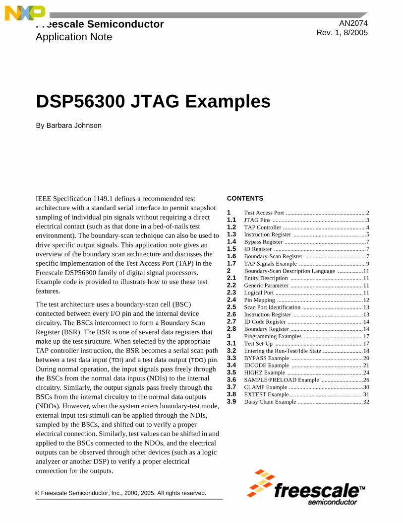
The test architecture uses a boundary-scan cell (BSC) connected between every I/O pin and the internal device circuitry. The BSCs interconnect to form a Boundary Scan Register (BSR). The BSR is one of several data registers that make up the test structure. When selected by the appropriate TAP controller instruction, the BSR becomes a serial scan path between a test data input (TDI) and a test data output (TDO) pin. During normal operation, the input signals pass freely through the BSCs from the normal data inputs (NDIs) to the internal circuitry. Similarly, the output signals pass freely through the BSCs from the internal circuitry to the normal data outputs (NDOs). However, when the system enters boundary-test mode, external input test stimuli can be applied through the NDIs, sampled by the BSCs, and shifted out to verify a proper electrical connection. Similarly, test values can be shifted in and applied to the BSCs connected to the NDOs, and the electrical outputs can be observed through other devices (such as a logic analyzer or another DSP) to verify a proper electrical connection for the outputs.
© Freescale Semiconductor, Inc., 2000, 2005. All rights reserved.
Test Access Port
Figure 1 shows the BSC block diagram.
Figure 1. Boundary Scan Cells
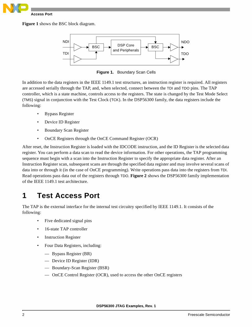
In addition to the data registers in the IEEE 1149.1 test structures, an instruction register is required. All registers are accessed serially through the TAP, and, when selected, connect between the TDI and TDO pins. The TAP controller, which is a state machine, controls access to the registers. The state is changed by the Test Mode Select (TMS) signal in conjunction with the Test Clock (TCK). In the DSP56300 family, the data registers include the following:
• Bypass Register
• Device ID Register
• Boundary Scan Register
• OnCE Registers through the OnCE Command Register (OCR)
After reset, the Instruction Register is loaded with the IDCODE instruction, and the ID Register is the selected data register. You can perform a data scan to read the device information. For other operations, the TAP programming sequence must begin with a scan into the Instruction Register to specify the appropriate data register. After an Instruction Register scan, subsequent scans are through the specified data register and may involve several scans of data into or through it (in the case of OnCE programming). Write operations pass data into the registers from TDI. Read operations pass data out of the registers through TDO. Figure 2 shows the DSP56300 family implementation of the IEEE 1149.1 test architecture.
1 Test Access PortThe TAP is the external interface for the internal test circuitry specified by IEEE 1149.1. It consists of the following:
• Five dedicated signal pins
• 16-state TAP controller
• Instruction Register
• Four Data Registers, including:
— Bypass Register (BR)
— Device ID Register (IDR)
— Boundary-Scan Register (BSR)
— OnCE Control Register (OCR), used to access the other OnCE registers
NDI
TDI
BSC BSCDSP CoreNDO
TDOand Peripherals
DSP56300 JTAG Examples, Rev. 1
2 Freescale Semiconductor
Test Access Port
Figure 2. Boundary Scan Architecture
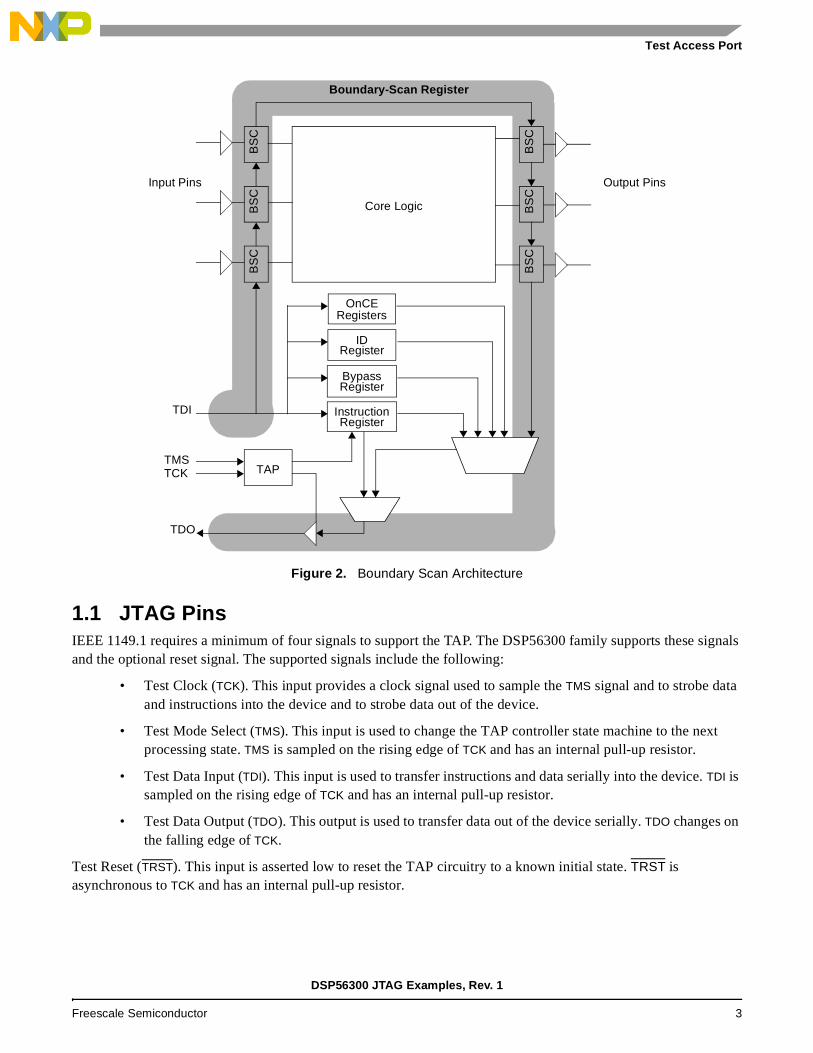
1.1 JTAG PinsIEEE 1149.1 requires a minimum of four signals to support the TAP. The DSP56300 family supports these signals and the optional reset signal. The supported signals include the following:
• Test Clock (TCK). This input provides a clock signal used to sample the TMS signal and to strobe data and instructions into the device and to strobe data out of the device.
• Test Mode Select (TMS). This input is used to change the TAP controller state machine to the next processing state. TMS is sampled on the rising edge of TCK and has an internal pull-up resistor.
• Test Data Input (TDI). This input is used to transfer instructions and data serially into the device. TDI is sampled on the rising edge of TCK and has an internal pull-up resistor.
• Test Data Output (TDO). This output is used to transfer data out of the device serially. TDO changes on the falling edge of TCK.
Test Reset (TRST). This input is asserted low to reset the TAP circuitry to a known initial state. TRST is asynchronous to TCK and has an internal pull-up resistor.
BS
CB
SC
BS
C
BS
CB
SC
BS
C
BypassRegister
TAP
InstructionRegister
IDRegister
OnCERegisters
Core Logic
Boundary-Scan Register
Input Pins Output Pins
TDI
TMSTCK
TDO
DSP56300 JTAG Examples, Rev. 1
Freescale Semiconductor 3
Test Access Port
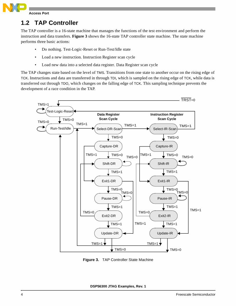
1.2 TAP ControllerThe TAP controller is a 16-state machine that manages the functions of the test environment and perform the instruction and data transfers. Figure 3 shows the 16-state TAP controller state machine. The state machine performs three basic actions:
• Do nothing. Test-Logic-Reset or Run-Test/Idle state
• Load a new instruction. Instruction Register scan cycle
• Load new data into a selected data register. Data Register scan cycle
The TAP changes state based on the level of TMS. Transitions from one state to another occur on the rising edge of TCK. Instructions and data are transferred in through TDI, which is sampled on the rising edge of TCK, while data is transferred out through TDO, which changes on the falling edge of TCK. This sampling technique prevents the development of a race condition in the TAP.
Figure 3. TAP Controller State Machine
Test-Logic-Reset
Run-Test/Idle Select-DR-Scan
Capture-DR
Shift-DR
Exit1-DR
Pause-DR
Exit2-DR
Update-DR
Select-IR-Scan
Capture-IR
Shift-IR
Exit1-IR
Pause-IR
Exit2-IR
Update-IR
TMS=1
TMS=0
TMS=0
TMS=0
TMS=0
TMS=0
TMS=0TMS=0 TMS=0
TMS=0TMS=0
TMS=0 TMS=0
TMS=0 TMS=0
TMS=1 TMS=1 TMS=1
TMS=1 TMS=1
TMS=1
TMS=1
TMS=1
TMS=1
TMS=0 TMS=0
TMS=1 TMS=1
TMS=1 TMS=1
TMS=1
TMS=1
Data Register Instruction RegisterScan CycleScan Cycle
TRST=0
DSP56300 JTAG Examples, Rev. 1
4 Freescale Semiconductor
Test Access Port
At power up or during normal operation of the DSP, TRST can be asserted to initialize the test controller. This immediately places the TAP in the Test-Logic-Reset state. The TAP can also be forced into the Test-Logic-Reset state by driving TMS high for five TCK cycles. Five TCK cycles are the maximum number required to transition the TAP to the Test-Logic-Reset state from any of the other states when TMS is held high. In the Test-Logic-Reset state, the TAP issues an internal reset signal that places all test logic in a condition that does not impede normal DSP operation. It locks the IDCODE instruction into the Instruction Register and selects the device ID Register as the default data register at reset.
From the Test-Logic-Reset state, the TAP moves to the Run-Test/Idle state when TMS is pulled low. As long as TMS is held low, the TAP stays in the Idle state. From this state, driving TMS high moves the TAP to the data register scan cycle. The TAP cannot remain in the Select-DR-Scan state for more than one TCK cycle. Driving TMS low for one TCK cycle causes the TAP to begin the data register scan process, moving to the Capture_DR state. Keeping TMS high for one more TCK cycle moves the TAP to the beginning of the Instruction Register scan cycle (Select-IR-Scan state).
After reset, you can read the Device ID Register (default). To perform any other action, you must move the TAP to the Instruction Register scan cycle to select an appropriate data register. For either type of scan cycle (data register or instruction register), the first action in the scan cycle is a capture operation. The Capture-DR state enables the data register indicated by the current Instruction Register contents. The Capture-IR state enables access to the Instruction Register.
From the Capture state, the TAP transitions either to the Shift or to the Exit1 state. The Shift state allows test data or a new instruction to be shifted in or status information to be shifted out for inspection. Following the Shift state, the TAP either returns to the Run-Test/Idle state, via the Exit1 and Update states, or enters the Pause state, via Exit1. The Pause state allows data shifting through either the selected data register or Instruction Register to be temporarily suspended while a required operation is performed. From the Pause state, shifting can resume by re-entering the Shift state via the Exit2 state, or it can be terminated by entering the Run-Test/Idle state via the Exit2 and Update states.
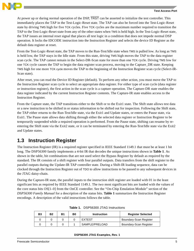
1.3 Instruction RegisterThe Instruction Register (IR) is a required register specified in IEEE Standard 1149.1 that must be at least 1 bit long. The DSP56300 family implements a 4-bit IR that decodes the unique instructions shown in Table 1. As shown in the table, bit combinations that are not used select the Bypass Register by default as required by the standard. The IR consists of a shift register with four parallel outputs. Data transfers from the shift register to the parallel outputs during the Update-IR TAP controller state. During a Shift-IR loading sequence, data can be clocked through the Instruction Register out of TDO to allow instructions to be passed to any subsequent devices in the JTAG daisy-chain.
During the Capture-IR state, the parallel inputs to the instruction shift register are loaded with 01 in the least significant bits as required by IEEE Standard 1149.1. The two most significant bits are loaded with the values of the core status bits OS[1–0] from the OnCE controller. See the “On-Chip Emulation Module” section of the DSP56300 Family Manual for a description of the status bits. Table 1 summarizes the Instruction Register encodings. A description of the valid instructions follows the table.
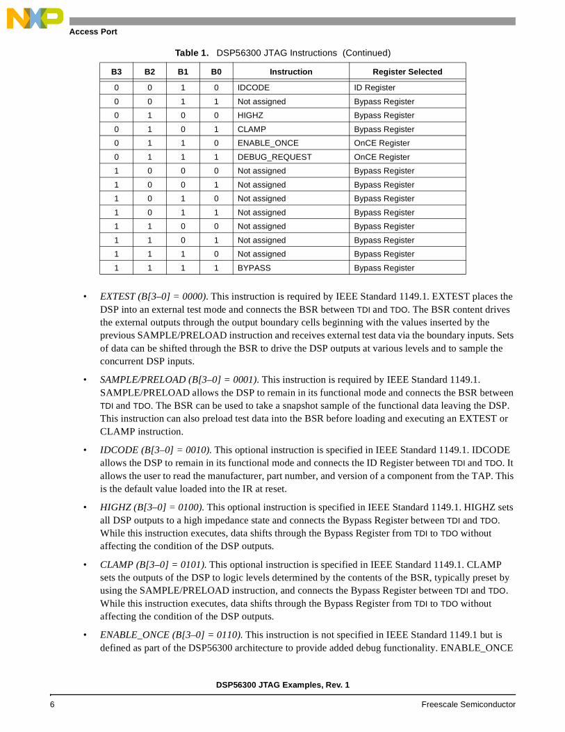
Table 1. DSP56300 JTAG Instructions
B3 B2 B1 B0 Instruction Register Selected
0 0 0 0 EXTEST Boundary-Scan Register
0 0 0 1 SAMPLE/PRELOAD Boundary-Scan Register
DSP56300 JTAG Examples, Rev. 1
Freescale Semiconductor 5
Test Access Port
• EXTEST (B[3–0] = 0000). This instruction is required by IEEE Standard 1149.1. EXTEST places the DSP into an external test mode and connects the BSR between TDI and TDO. The BSR content drives the external outputs through the output boundary cells beginning with the values inserted by the previous SAMPLE/PRELOAD instruction and receives external test data via the boundary inputs. Sets of data can be shifted through the BSR to drive the DSP outputs at various levels and to sample the concurrent DSP inputs.
• SAMPLE/PRELOAD (B[3–0] = 0001). This instruction is required by IEEE Standard 1149.1. SAMPLE/PRELOAD allows the DSP to remain in its functional mode and connects the BSR between TDI and TDO. The BSR can be used to take a snapshot sample of the functional data leaving the DSP. This instruction can also preload test data into the BSR before loading and executing an EXTEST or CLAMP instruction.
• IDCODE (B[3–0] = 0010). This optional instruction is specified in IEEE Standard 1149.1. IDCODE allows the DSP to remain in its functional mode and connects the ID Register between TDI and TDO. It allows the user to read the manufacturer, part number, and version of a component from the TAP. This is the default value loaded into the IR at reset.
• HIGHZ (B[3–0] = 0100). This optional instruction is specified in IEEE Standard 1149.1. HIGHZ sets all DSP outputs to a high impedance state and connects the Bypass Register between TDI and TDO. While this instruction executes, data shifts through the Bypass Register from TDI to TDO without affecting the condition of the DSP outputs.
• CLAMP (B[3–0] = 0101). This optional instruction is specified in IEEE Standard 1149.1. CLAMP sets the outputs of the DSP to logic levels determined by the contents of the BSR, typically preset by using the SAMPLE/PRELOAD instruction, and connects the Bypass Register between TDI and TDO. While this instruction executes, data shifts through the Bypass Register from TDI to TDO without affecting the condition of the DSP outputs.
• ENABLE_ONCE (B[3–0] = 0110). This instruction is not specified in IEEE Standard 1149.1 but is defined as part of the DSP56300 architecture to provide added debug functionality. ENABLE_ONCE
0 0 1 0 IDCODE ID Register
0 0 1 1 Not assigned Bypass Register
0 1 0 0 HIGHZ Bypass Register
0 1 0 1 CLAMP Bypass Register
0 1 1 0 ENABLE_ONCE OnCE Register
0 1 1 1 DEBUG_REQUEST OnCE Register
1 0 0 0 Not assigned Bypass Register
1 0 0 1 Not assigned Bypass Register
1 0 1 0 Not assigned Bypass Register
1 0 1 1 Not assigned Bypass Register
1 1 0 0 Not assigned Bypass Register
1 1 0 1 Not assigned Bypass Register
1 1 1 0 Not assigned Bypass Register
1 1 1 1 BYPASS Bypass Register
Table 1. DSP56300 JTAG Instructions (Continued)
B3 B2 B1 B0 Instruction Register Selected
DSP56300 JTAG Examples, Rev. 1
6 Freescale Semiconductor
Test Access Port
allows you to perform system debug functions and connects the OnCE Control Register (OCR) between TDI and TDO. The OCR writes data to and reads data from the other OnCE registers depending on which OnCE instruction is executed.
• DEBUG_REQUEST (B[3–0] = 0111). This instruction is not specified in IEEE Standard 1149.1 but is defined as part of the DSP56300 architecture to provide added debug functionality. DEBUG_REQUEST generates a debug request signal to the DSP56300 core. When this instruction is decoded, the TDI and TDO pins remain connected to the Instruction Register until the core signals that it has entered Debug mode (indicated by a value of 1101 being shifted out from the Instruction Register). The external JTAG controller must continue to shift in the DEBUG_REQUEST instruction while polling the status bits that are shifted out until the system enters Debug mode. After the acknowledgment of Debug mode is received, the external JTAG controller must issue the ENABLE_ONCE instruction to allow the user to perform system debug functions.
• BYPASS (B[3–0] = 1111). This instruction is required by IEEE Standard 1149.1. BYPASS allows the DSP to remain in its functional mode and connects the Bypass Register between TDI and TDO. It allows serial data to pass through the DSP from TDI to TDO without affecting the DSP operation.
1.4 Bypass RegisterThe Bypass Register provides a single-bit scan path between TDI and TDO. It enhances test efficiency when a device other than the DSP56300 core-based device becomes the device under test. When the Bypass Register is selected by the current instruction, the shift register stage is set to a logic 0 on the rising edge of TCK in the Capture-DR controller state. Therefore, the first bit shifted out after the Bypass Register is selected is always 0.
1.5 ID RegisterThe 32-bit ID Register stores values that identify the device manufacturer, part number, and version and is selected by the IDCODE instruction. It can be used to distinguish specific IEEE 1149.1-compliant parts in a daisy-chained system. The least significant bit (bit 0) is always set to logic 1, as required by the standard; this bit is an identity packing bit that indicates valid data. Table 2 summarizes the ID Register.
1.6 Boundary-Scan RegisterThe Boundary-Scan Register in the DSP56300 devices contain bits for all signal, clock, and control pins. All bidirectional pins have a single register bit and an associated control bit in the BSR. In the Update-DR state, the register contains valid stimuli data. In the Capture-DR state, the Boundary-Scan Register samples data. Data
Table 2. ID Register
Bit Description Value
31–28 Version Information 0000 Version 0
27–22 Design Center Number 000110 Freescale Semiconductor Israel
21–17 Core Number 00000 DSP56300
16–12 Chip Derivative Number 00011 DSP56303
11–1 Manufacturer Identity 00000001110 Freescale
0 Pre-set to logic 1 1 Pre-set to logic 1
DSP56300 JTAG Examples, Rev. 1
Freescale Semiconductor 7
Test Access Port
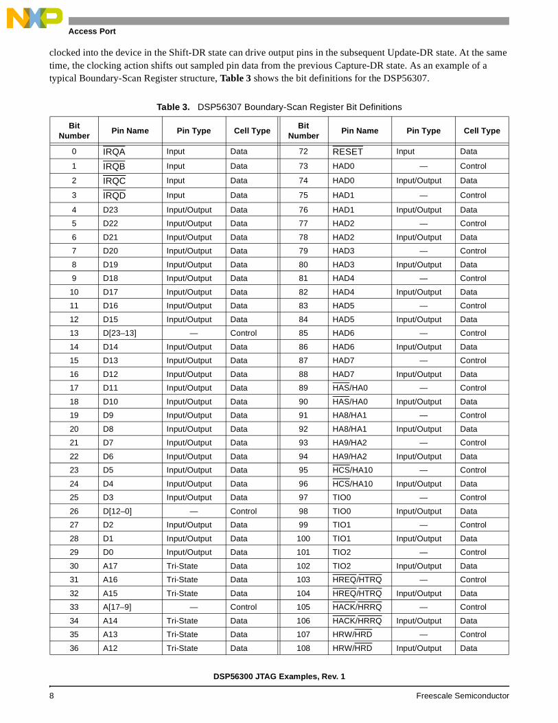
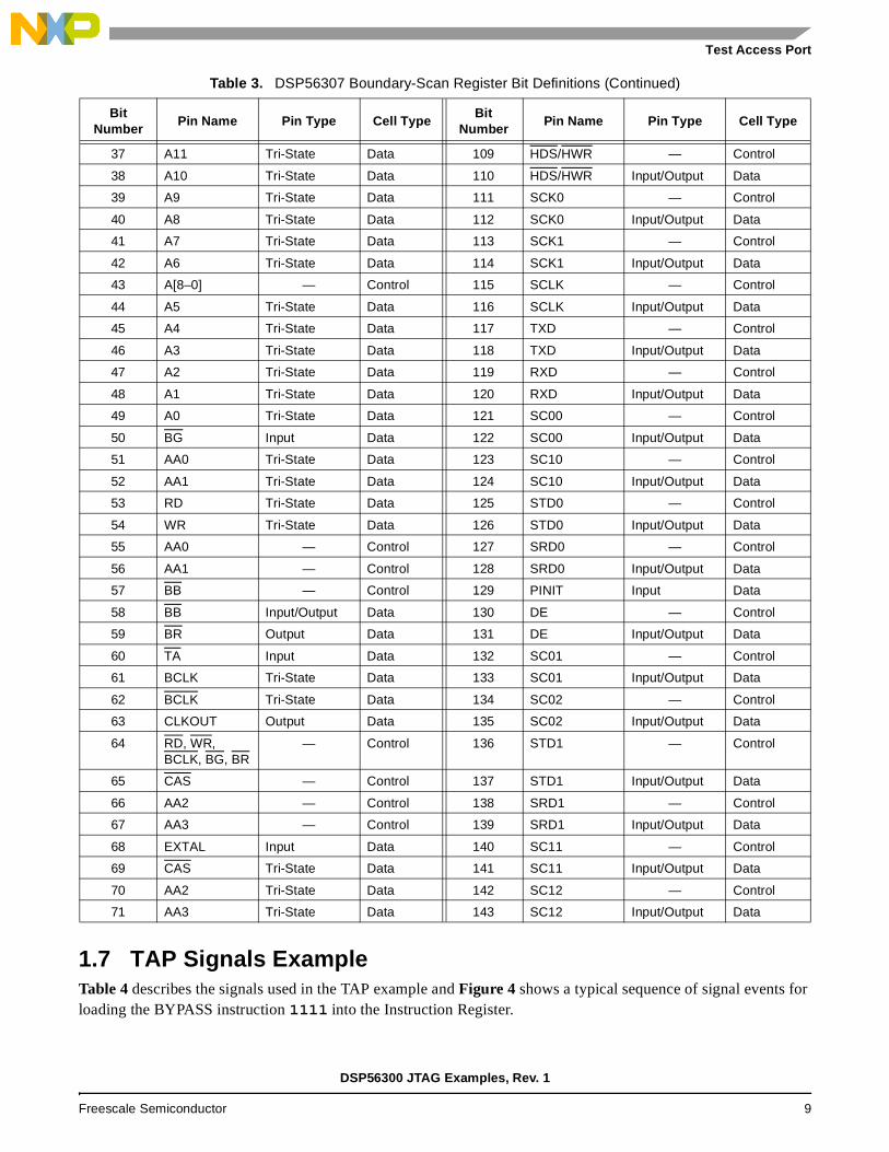
clocked into the device in the Shift-DR state can drive output pins in the subsequent Update-DR state. At the same time, the clocking action shifts out sampled pin data from the previous Capture-DR state. As an example of a typical Boundary-Scan Register structure, Table 3 shows the bit definitions for the DSP56307.
Table 3. DSP56307 Boundary-Scan Register Bit Definitions
Bit Number
Pin Name Pin Type Cell TypeBit
NumberPin Name Pin Type Cell Type
0 IRQA Input Data 72 RESET Input Data
1 IRQB Input Data 73 HAD0 — Control
2 IRQC Input Data 74 HAD0 Input/Output Data
3 IRQD Input Data 75 HAD1 — Control
4 D23 Input/Output Data 76 HAD1 Input/Output Data
5 D22 Input/Output Data 77 HAD2 — Control
6 D21 Input/Output Data 78 HAD2 Input/Output Data
7 D20 Input/Output Data 79 HAD3 — Control
8 D19 Input/Output Data 80 HAD3 Input/Output Data
9 D18 Input/Output Data 81 HAD4 — Control
10 D17 Input/Output Data 82 HAD4 Input/Output Data
11 D16 Input/Output Data 83 HAD5 — Control
12 D15 Input/Output Data 84 HAD5 Input/Output Data
13 D[23–13] — Control 85 HAD6 — Control
14 D14 Input/Output Data 86 HAD6 Input/Output Data
15 D13 Input/Output Data 87 HAD7 — Control
16 D12 Input/Output Data 88 HAD7 Input/Output Data
17 D11 Input/Output Data 89 HAS/HA0 — Control
18 D10 Input/Output Data 90 HAS/HA0 Input/Output Data
19 D9 Input/Output Data 91 HA8/HA1 — Control
20 D8 Input/Output Data 92 HA8/HA1 Input/Output Data
21 D7 Input/Output Data 93 HA9/HA2 — Control
22 D6 Input/Output Data 94 HA9/HA2 Input/Output Data
23 D5 Input/Output Data 95 HCS/HA10 — Control
24 D4 Input/Output Data 96 HCS/HA10 Input/Output Data
25 D3 Input/Output Data 97 TIO0 — Control
26 D[12–0] — Control 98 TIO0 Input/Output Data
27 D2 Input/Output Data 99 TIO1 — Control
28 D1 Input/Output Data 100 TIO1 Input/Output Data
29 D0 Input/Output Data 101 TIO2 — Control
30 A17 Tri-State Data 102 TIO2 Input/Output Data
31 A16 Tri-State Data 103 HREQ/HTRQ — Control
32 A15 Tri-State Data 104 HREQ/HTRQ Input/Output Data
33 A[17–9] — Control 105 HACK/HRRQ — Control
34 A14 Tri-State Data 106 HACK/HRRQ Input/Output Data
35 A13 Tri-State Data 107 HRW/HRD — Control
36 A12 Tri-State Data 108 HRW/HRD Input/Output Data
DSP56300 JTAG Examples, Rev. 1
8 Freescale Semiconductor
Test Access Port
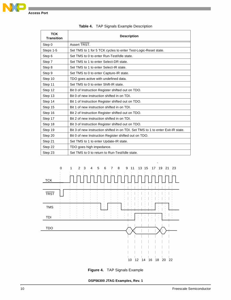
1.7 TAP Signals ExampleTable 4 describes the signals used in the TAP example and Figure 4 shows a typical sequence of signal events for loading the BYPASS instruction 1111 into the Instruction Register.
37 A11 Tri-State Data 109 HDS/HWR — Control
38 A10 Tri-State Data 110 HDS/HWR Input/Output Data
39 A9 Tri-State Data 111 SCK0 — Control
40 A8 Tri-State Data 112 SCK0 Input/Output Data
41 A7 Tri-State Data 113 SCK1 — Control
42 A6 Tri-State Data 114 SCK1 Input/Output Data
43 A[8–0] — Control 115 SCLK — Control
44 A5 Tri-State Data 116 SCLK Input/Output Data
45 A4 Tri-State Data 117 TXD — Control
46 A3 Tri-State Data 118 TXD Input/Output Data
47 A2 Tri-State Data 119 RXD — Control
48 A1 Tri-State Data 120 RXD Input/Output Data
49 A0 Tri-State Data 121 SC00 — Control
50 BG Input Data 122 SC00 Input/Output Data
51 AA0 Tri-State Data 123 SC10 — Control
52 AA1 Tri-State Data 124 SC10 Input/Output Data
53 RD Tri-State Data 125 STD0 — Control
54 WR Tri-State Data 126 STD0 Input/Output Data
55 AA0 — Control 127 SRD0 — Control
56 AA1 — Control 128 SRD0 Input/Output Data
57 BB — Control 129 PINIT Input Data
58 BB Input/Output Data 130 DE — Control
59 BR Output Data 131 DE Input/Output Data
60 TA Input Data 132 SC01 — Control
61 BCLK Tri-State Data 133 SC01 Input/Output Data
62 BCLK Tri-State Data 134 SC02 — Control
63 CLKOUT Output Data 135 SC02 Input/Output Data
64 RD, WR, BCLK, BG, BR
— Control 136 STD1 — Control
65 CAS — Control 137 STD1 Input/Output Data
66 AA2 — Control 138 SRD1 — Control
67 AA3 — Control 139 SRD1 Input/Output Data
68 EXTAL Input Data 140 SC11 — Control
69 CAS Tri-State Data 141 SC11 Input/Output Data
70 AA2 Tri-State Data 142 SC12 — Control
71 AA3 Tri-State Data 143 SC12 Input/Output Data
Table 3. DSP56307 Boundary-Scan Register Bit Definitions (Continued)
Bit Number
Pin Name Pin Type Cell TypeBit
NumberPin Name Pin Type Cell Type
DSP56300 JTAG Examples, Rev. 1
Freescale Semiconductor 9
Test Access Port
Figure 4. TAP Signals Example
Table 4. TAP Signals Example Description
TCK Transition
Description
Step 0 Assert TRST.
Steps 1-5 Set TMS to 1 for 5 TCK cycles to enter Test-Logic-Reset state.
Step 6 Set TMS to 0 to enter Run-Test/Idle state.
Step 7 Set TMS to 1 to enter Select-DR state.
Step 8 Set TMS to 1 to enter Select-IR state.
Step 9 Set TMS to 0 to enter Capture-IR state.
Step 10 TDO goes active with undefined data.
Step 11 Set TMS to 0 to enter Shift-IR state.
Step 12 Bit 0 of Instruction Register shifted out on TDO.
Step 13 Bit 0 of new instruction shifted in on TDI.
Step 14 Bit 1 of Instruction Register shifted out on TDO.
Step 15 Bit 1 of new instruction shifted in on TDI.
Step 16 Bit 2 of Instruction Register shifted out on TDO.
Step 17 Bit 2 of new instruction shifted in on TDI.
Step 18 Bit 3 of Instruction Register shifted out on TDO.
Step 19 Bit 3 of new instruction shifted in on TDI. Set TMS to 1 to enter Exit-IR state.
Step 20 Bit 0 of new Instruction Register shifted out on TDO.
Step 21 Set TMS to 1 to enter Update-IR state.
Step 22 TDO goes high impedance.
Step 23 Set TMS to 0 to return to Run-Test/Idle state.
TCK
9
TRST
TDI
TMS
1 2 3 4 5 6 7 8 9 11 13 15 17 19 21 230
10 12 14 16 18 20 22
TDO
DSP56300 JTAG Examples, Rev. 1
10 Freescale Semiconductor
Boundary-Scan Description Language
2 Boundary-Scan Description LanguageBoundary-Scan Description Language (BSDL) describes how IEEE 1149.1 is implemented in a device and how the device operates. A BSDL description for a device consists of an entity description, a generic parameter, a logical port description, pin mapping, a scan port identification, an Instruction Register description, an ID code description, and a Boundary Register description. BSDL files for the DSP56300 family can be downloaded from: http://www.mot.com/SPS/DSP/documentation/DSP56300.html
2.1 Entity DescriptionThe entity description gives the name of the device. It begins with an entity statement and terminates with an end statement. Example 1 shows the DSP56307 entity description.
Example 1. Entity Description
entity DSP56307 is
...
end DSP56307;
2.2 Generic ParameterA generic parameter is a parameter that can come from outside the entity, or it can be defaulted such as the package type. Example 2 shows the 196-pin PBGA DSP56307 generic parameter.
Example 2. Generic Parameter
generic (PHYSICAL_PIN_MAP : string := "PBGA196");
2.3 Logical PortThe logical port description gives logical names to the I/O pins and specifies whether the signals are input, output, bidirectional, or linkage (power supply). Example 3 shows the DSP56307 logical port description.
Example 3. Logical Port Description
port ( DE_N: inout bit;
SC02: inout bit;
SC01: inout bit;
...
MODD: in bit;
MODC: in bit;
...
D: inout bit_vector(0 to 23);
A: out bit_vector(0 to 17);
...
DVCC: linkage bit_vector(0 to 3);
AVCC: linkage bit_vector(0 to 2);
...
DSP56300 JTAG Examples, Rev. 1
Freescale Semiconductor 11
Boundary-Scan Description Language
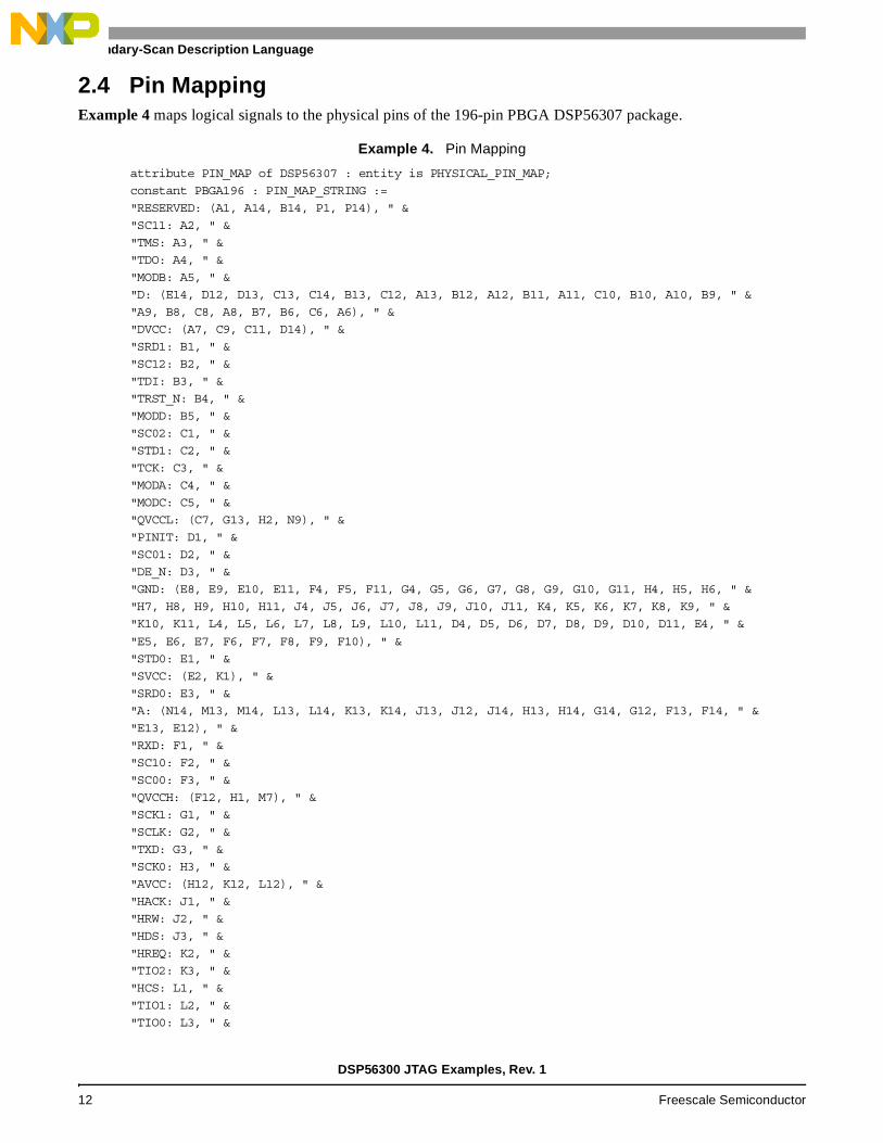
2.4 Pin MappingExample 4 maps logical signals to the physical pins of the 196-pin PBGA DSP56307 package.
Example 4. Pin Mapping
attribute PIN_MAP of DSP56307 : entity is PHYSICAL_PIN_MAP;
constant PBGA196 : PIN_MAP_STRING :=
"RESERVED: (A1, A14, B14, P1, P14), " &
"SC11: A2, " &
"TMS: A3, " &
"TDO: A4, " &
"MODB: A5, " &
"D: (E14, D12, D13, C13, C14, B13, C12, A13, B12, A12, B11, A11, C10, B10, A10, B9, " &
"A9, B8, C8, A8, B7, B6, C6, A6), " &
"DVCC: (A7, C9, C11, D14), " &
"SRD1: B1, " &
"SC12: B2, " &
"TDI: B3, " &
"TRST_N: B4, " &
"MODD: B5, " &
"SC02: C1, " &
"STD1: C2, " &
"TCK: C3, " &
"MODA: C4, " &
"MODC: C5, " &
"QVCCL: (C7, G13, H2, N9), " &
"PINIT: D1, " &
"SC01: D2, " &
"DE_N: D3, " &
"GND: (E8, E9, E10, E11, F4, F5, F11, G4, G5, G6, G7, G8, G9, G10, G11, H4, H5, H6, " &
"H7, H8, H9, H10, H11, J4, J5, J6, J7, J8, J9, J10, J11, K4, K5, K6, K7, K8, K9, " &
"K10, K11, L4, L5, L6, L7, L8, L9, L10, L11, D4, D5, D6, D7, D8, D9, D10, D11, E4, " &
"E5, E6, E7, F6, F7, F8, F9, F10), " &
"STD0: E1, " &
"SVCC: (E2, K1), " &
"SRD0: E3, " &
"A: (N14, M13, M14, L13, L14, K13, K14, J13, J12, J14, H13, H14, G14, G12, F13, F14, " &
"E13, E12), " &
"RXD: F1, " &
"SC10: F2, " &
"SC00: F3, " &
"QVCCH: (F12, H1, M7), " &
"SCK1: G1, " &
"SCLK: G2, " &
"TXD: G3, " &
"SCK0: H3, " &
"AVCC: (H12, K12, L12), " &
"HACK: J1, " &
"HRW: J2, " &
"HDS: J3, " &
"HREQ: K2, " &
"TIO2: K3, " &
"HCS: L1, " &
"TIO1: L2, " &
"TIO0: L3, " &
DSP56300 JTAG Examples, Rev. 1
12 Freescale Semiconductor
Boundary-Scan Description Language
"HA8: M1, " &
"HA9: M2, " &
"HAS: M3, " &
"HVCC: M4, " &
"HAD: (M5, P4, N4, P3, N3, P2, N1, N2), " &
"PVCC: M6, " &
"EXTAL: M8, " &
"CLKOUT: M9, " &
"BCLK_N: M10, " &
"WR_N: M11, " &
"RD_N: M12, " &
"RESET_N: N5, " &
"PGND: N6, " &
"AA: (N13, P12, P7, N7), " &
"CAS_N: N8, " &
"BCLK: N10, " &
"BR_N: N11, " &
"CVCC: (N12, P9), " &
"PCAP: P5, " &
"PGND1: P6, " &
"XTAL: P8, " &
"TA_N: P10, " &
"BB_N: P11, " &
"BG_N: P13 ";
2.5 Scan Port IdentificationThe scan port identification statements define the device TAP. Example 5 shows the DSP56307 scan port identification.
Example 5. Scan Port Identification
attribute TAP_SCAN_IN of TDI : signal is true;
attribute TAP_SCAN_OUT of TDO : signal is true;
attribute TAP_SCAN_MODE of TMS : signal is true;
attribute TAP_SCAN_RESET of TRST_N : signal is true;
attribute TAP_SCAN_CLOCK of TCK : signal is (20.0e6, BOTH);
2.6 Instruction RegisterThe Instruction Register description identifies the device-dependent characteristics of the identification register. Example 6 shows the DSP56307 Instruction Register description. The Instruction Register description defines the Instruction Register length as 4 bits and gives the instruction opcode definitions. It also defines that in the Capture-IR state, the parallel inputs to the instruction shift register are loaded with 01 in the least significant bits.
Example 6. Instruction Register Description
attribute INSTRUCTION_LENGTH of DSP56307 : entity is 4;
attribute INSTRUCTION_OPCODE of DSP56307 : entity is
"EXTEST (0000)," &
"SAMPLE (0001)," &
"IDCODE (0010)," &
"CLAMP (0101)," &
"HIGHZ (0100)," &
"ENABLE_ONCE (0110)," &
DSP56300 JTAG Examples, Rev. 1
Freescale Semiconductor 13
Boundary-Scan Description Language
"DEBUG_REQUEST (0111)," &
"BYPASS (1111)";
attribute INSTRUCTION_CAPTURE of DSP56307 : entity is "0001";
2.7 ID Code RegisterThe ID code register description identifies the values captured in the device identification register when the IDCODE instruction is executed. Example 7 shows the DSP56307 ID code register description.
Example 7. ID Code Register Description
attribute IDCODE_REGISTER of DSP56307 : entity is
"0000" & -- version
"000110" & -- manufacturer’s use
"0000000111" & -- sequence number
"00000001110" & -- manufacturer identity
"1"; -- 1149.1 requirement
2.8 Boundary RegisterThe Boundary Register description lists the boundary-scan cells and gives information regarding the cell type and associated control. Example 8 shows the DSP56307 boundary scan description. The Boundary Register description defines the Boundary-Scan Register length as 144 bits and gives the instruction opcode definitions
Example 8. Boundary Scan Description
attribute BOUNDARY_LENGTH of DSP56307 : entity is 144;
attribute BOUNDARY_REGISTER of DSP56307 : entity is
-- num cell port func safe [ccell dis rslt]
"0 (BC_1, MODA, input, X)," &
"1 (BC_1, MODB, input, X)," &
"2 (BC_1, MODC, input, X)," &
"3 (BC_1, MODD, input, X)," &
"4 (BC_6, D(23), bidir, X, 13, 1, Z)," &
"5 (BC_6, D(22), bidir, X, 13, 1, Z)," &
"6 (BC_6, D(21), bidir, X, 13, 1, Z)," &
"7 (BC_6, D(20), bidir, X, 13, 1, Z)," &
"8 (BC_6, D(19), bidir, X, 13, 1, Z)," &
"9 (BC_6, D(18), bidir, X, 13, 1, Z)," &
"10 (BC_6, D(17), bidir, X, 13, 1, Z)," &
"11 (BC_6, D(16), bidir, X, 13, 1, Z)," &
"12 (BC_6, D(15), bidir, X, 13, 1, Z)," &
"13 (BC_1, *, control, 1)," &
"14 (BC_6, D(14), bidir, X, 13, 1, Z)," &
"15 (BC_6, D(13), bidir, X, 13, 1, Z)," &
"16 (BC_6, D(12), bidir, X, 13, 1, Z)," &
"17 (BC_6, D(11), bidir, X, 26, 1, Z)," &
"18 (BC_6, D(10), bidir, X, 26, 1, Z)," &
"19 (BC_6, D(9), bidir, X, 26, 1, Z)," &
-- num cell port func safe [ccell dis rslt]
"20 (BC_6, D(8), bidir, X, 26, 1, Z)," &
"21 (BC_6, D(7), bidir, X, 26, 1, Z)," &
"22 (BC_6, D(6), bidir, X, 26, 1, Z)," &
"23 (BC_6, D(5), bidir, X, 26, 1, Z)," &
"24 (BC_6, D(4), bidir, X, 26, 1, Z)," &
"25 (BC_6, D(3), bidir, X, 26, 1, Z)," &
DSP56300 JTAG Examples, Rev. 1
14 Freescale Semiconductor
Boundary-Scan Description Language
"26 (BC_1, *, control, 1)," &
"27 (BC_6, D(2), bidir, X, 26, 1, Z)," &
"28 (BC_6, D(1), bidir, X, 26, 1, Z)," &
"29 (BC_6, D(0), bidir, X, 26, 1, Z)," &
"30 (BC_1, A(17), output3, X, 33, 1, Z)," &
"31 (BC_1, A(16), output3, X, 33, 1, Z)," &
"32 (BC_1, A(15), output3, X, 33, 1, Z)," &
"33 (BC_1, *, control, 1)," &
"34 (BC_1, A(14), output3, X, 33, 1, Z)," &
"35 (BC_1, A(13), output3, X, 33, 1, Z)," &
"36 (BC_1, A(12), output3, X, 33, 1, Z)," &
"37 (BC_1, A(11), output3, X, 33, 1, Z)," &
"38 (BC_1, A(10), output3, X, 33, 1, Z)," &
"39 (BC_1, A(9), output3, X, 33, 1, Z)," &
-- num cell port func safe [ccell dis rslt]
"40 (BC_1, A(8), output3, X, 43, 1, Z)," &
"41 (BC_1, A(7), output3, X, 43, 1, Z)," &
"42 (BC_1, A(6), output3, X, 43, 1, Z)," &
"43 (BC_1, *, control, 1)," &
"44 (BC_1, A(5), output3, X, 43, 1, Z)," &
"45 (BC_1, A(4), output3, X, 43, 1, Z)," &
"46 (BC_1, A(3), output3, X, 43, 1, Z)," &
"47 (BC_1, A(2), output3, X, 43, 1, Z)," &
"48 (BC_1, A(1), output3, X, 43, 1, Z)," &
"49 (BC_1, A(0), output3, X, 43, 1, Z)," &
"50 (BC_1, BG_N, input, X)," &
"51 (BC_1, AA(0), output3, X, 55, 1, Z)," &
"52 (BC_1, AA(1), output3, X, 56, 1, Z)," &
"53 (BC_1, RD_N, output3, X, 64, 1, Z)," &
"54 (BC_1, WR_N, output3, X, 64, 1, Z)," &
"55 (BC_1, *, control, 1)," &
"56 (BC_1, *, control, 1)," &
"57 (BC_1, *, control, 1)," &
"58 (BC_6, BB_N, bidir, X, 57, 1, Z)," &
"59 (BC_1, BR_N, output2, X)," &
-- num cell port func safe [ccell dis rslt]
"60 (BC_1, TA_N, input, X)," &
"61 (BC_1, BCLK_N, output3, X, 64, 1, Z)," &
"62 (BC_1, BCLK, output3, X, 64, 1, Z)," &
"63 (BC_1, CLKOUT, output2, X)," &
"64 (BC_1, *, control, 1)," &
"65 (BC_1, *, control, 1)," &
"66 (BC_1, *, control, 1)," &
"67 (BC_1, *, control, 1)," &
"68 (BC_1, EXTAL, input, X)," &
"69 (BC_1, CAS_N, output3, X, 65, 1, Z)," &
"70 (BC_1, AA(2), output3, X, 66, 1, Z)," &
"71 (BC_1, AA(3), output3, X, 67, 1, Z)," &
"72 (BC_1, RESET_N, input, X)," &
"73 (BC_1, *, control, 1)," &
"74 (BC_6, HAD(0), bidir, X, 73, 1, Z)," &
"75 (BC_1, *, control, 1)," &
"76 (BC_6, HAD(1), bidir, X, 75, 1, Z)," &
"77 (BC_1, *, control, 1)," &
"78 (BC_6, HAD(2), bidir, X, 77, 1, Z)," &
DSP56300 JTAG Examples, Rev. 1
Freescale Semiconductor 15
Boundary-Scan Description Language
"79 (BC_1, *, control, 1)," &
-- num cell port func safe [ccell dis rslt]
"80 (BC_6, HAD(3), bidir, X, 79, 1, Z)," &
"81 (BC_1, *, control, 1)," &
"82 (BC_6, HAD(4), bidir, X, 81, 1, Z)," &
"83 (BC_1, *, control, 1)," &
"84 (BC_6, HAD(5), bidir, X, 83, 1, Z)," &
"85 (BC_1, *, control, 1)," &
"86 (BC_6, HAD(6), bidir, X, 85, 1, Z)," &
"87 (BC_1, *, control, 1)," &
"88 (BC_6, HAD(7), bidir, X, 87, 1, Z)," &
"89 (BC_1, *, control, 1)," &
"90 (BC_6, HAS, bidir, X, 89, 1, Z)," &
"91 (BC_1, *, control, 1)," &
"92 (BC_6, HA8, bidir, X, 91, 1, Z)," &
"93 (BC_1, *, control, 1)," &
"94 (BC_6, HA9, bidir, X, 93, 1, Z)," &
"95 (BC_1, *, control, 1)," &
"96 (BC_6, HCS, bidir, X, 95, 1, Z)," &
"97 (BC_1, *, control, 1)," &
"98 (BC_6, TIO0, bidir, X, 97, 1, Z)," &
"99 (BC_1, *, control, 1)," &
-- num cell port func safe [ccell dis rslt]
"100 (BC_6, TIO1, bidir, X, 99, 1, Z)," &
"101 (BC_1, *, control, 1)," &
"102 (BC_6, TIO2, bidir, X, 101, 1, Z)," &
"103 (BC_1, *, control, 1)," &
"104 (BC_6, HREQ, bidir, X, 103, 1, Z)," &
"105 (BC_1, *, control, 1)," &
"106 (BC_6, HACK, bidir, X, 105, 1, Z)," &
"107 (BC_1, *, control, 1)," &
"108 (BC_6, HRW, bidir, X, 107, 1, Z)," &
"109 (BC_1, *, control, 1)," &
"110 (BC_6, HDS, bidir, X, 109, 1, Z)," &
"111 (BC_1, *, control, 1)," &
"112 (BC_6, SCK0, bidir, X, 111, 1, Z)," &
"113 (BC_1, *, control, 1)," &
"114 (BC_6, SCK1, bidir, X, 113, 1, Z)," &
"115 (BC_1, *, control, 1)," &
"116 (BC_6, SCLK, bidir, X, 115, 1, Z)," &
"117 (BC_1, *, control, 1)," &
"118 (BC_6, TXD, bidir, X, 117, 1, Z)," &
"119 (BC_1, *, control, 1)," &
-- num cell port func safe [ccell dis rslt]
"120 (BC_6, RXD, bidir, X, 119, 1, Z)," &
"121 (BC_1, *, control, 1)," &
"122 (BC_6, SC00, bidir, X, 121, 1, Z)," &
"123 (BC_1, *, control, 1)," &
"124 (BC_6, SC10, bidir, X, 123, 1, Z)," &
"125 (BC_1, *, control, 1)," &
"126 (BC_6, STD0, bidir, X, 125, 1, Z)," &
"127 (BC_1, *, control, 1)," &
"128 (BC_6, SRD0, bidir, X, 127, 1, Z)," &
"129 (BC_1, PINIT, input, X)," &
"130 (BC_1, *, control, 1)," &
DSP56300 JTAG Examples, Rev. 1
16 Freescale Semiconductor
Programming Examples
"131 (BC_6, DE_N, bidir, X, 130, 1, Pull1)," &
"132 (BC_1, *, control, 1)," &
"133 (BC_6, SC01, bidir, X, 132, 1, Z)," &
"134 (BC_1, *, control, 1)," &
"135 (BC_6, SC02, bidir, X, 134, 1, Z)," &
"136 (BC_1, *, control, 1)," &
"137 (BC_6, STD1, bidir, X, 136, 1, Z)," &
"138 (BC_1, *, control, 1)," &
"139 (BC_6, SRD1, bidir, X, 138, 1, Z)," &
-- num cell port func safe [ccell dis rslt]
"140 (BC_1, *, control, 1)," &
"141 (BC_6, SC11, bidir, X, 140, 1, Z)," &
"142 (BC_1, *, control, 1)," &
"143 (BC_6, SC12, bidir, X, 142, 1, Z)";
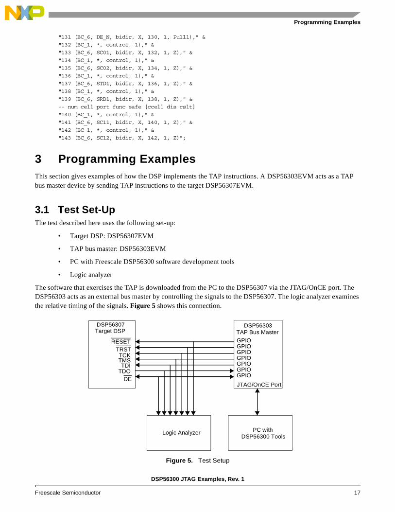
3 Programming ExamplesThis section gives examples of how the DSP implements the TAP instructions. A DSP56303EVM acts as a TAP bus master device by sending TAP instructions to the target DSP56307EVM.
3.1 Test Set-UpThe test described here uses the following set-up:
• Target DSP: DSP56307EVM
• TAP bus master: DSP56303EVM
• PC with Freescale DSP56300 software development tools
• Logic analyzer
The software that exercises the TAP is downloaded from the PC to the DSP56307 via the JTAG/OnCE port. The DSP56303 acts as an external bus master by controlling the signals to the DSP56307. The logic analyzer examines the relative timing of the signals. Figure 5 shows this connection.
Figure 5. Test Setup
RESETTRSTTCKTMSTDI
TDODE
GPIO
DSP56307 DSP56303
PC with
JTAG/OnCE Port
Logic Analyzer
GPIOGPIOGPIOGPIOGPIOGPIO
TAP Bus MasterTarget DSP
DSP56300 Tools
DSP56300 JTAG Examples, Rev. 1
Freescale Semiconductor 17
Programming Examples
3.2 Entering the Run-Test/Idle StateThe TAP controller must be initialized into the Test-Logic-Reset state to keep the test logic transparent to the DSP56300 system logic. This operation is done by performing one of the following after power-up:
• Asserting TRST
• Sampling TMS as a logical 1 for five consecutive TCK rising edges
The subroutine JTAG_RTI shown in Example 9 and described in Section 3.2.1 forces the TAP to enter the Test-Logic-Reset state (by asserting TMS for five TCK cycles) and then moves to the Run-Test/Idle state (by deasserting TMS).
Example 9. Entering Run-Test/Idle Routine
org x:
JTAG_RTI_SEQ:
dc $30 ; go to next state
dc $30 ; go to next state
dc $30 ; go to next state
dc $30 ; go to next state
dc $30 ; go to next state
dc $10 ; go to Run-Test-Idle
dc $00 ; EXIT
org p:$100
START
...
jsr JTAG_RTI
...
JTAG_RTI:
move #JTAG_RTI_SEQ,r0
jsr JTAG_EXECUTE
rts
3.2.1 JTAG_RTI SubroutineThe JTAG_RTI subroutine sends a sequence of 8-bit data to the JTAG_EXECUTE subroutine. The bit definitions are as Table 5 shows:
For example, a value of $30 (bit 5 = 1 and bit 4 = 1) indicates that TMS = 1 and TDI = 1 are sent on the rising edge of TCK. Since bit 2 = 0, TDO is not read on the falling edge of TCK. Thus, JTAG_RTI sends a value $30 five times to enter the Test-Reset-Logic state and then sends a value of $10 (TMS = 0, TDI =1, TDO is not read) to enter the Run-Test/Idle state.
Table 5. Subroutine Sequence Bit Definitions
7-6 5 4 3 2 1-0
Reserved TMS to send TDI to send Reserved Read TDO Reserved
DSP56300 JTAG Examples, Rev. 1
18 Freescale Semiconductor
Programming Examples
3.2.2 JTAG_EXECUTE SubroutineThe JTAG_EXECUTE subroutine performs the operations necessary to emulate the JTAG/OnCE operation. When the JTAG_RTI sends an 8-bit item of data, the JTAG_EXECUTE first determines if bit 2 is set to indicate that TDO needs to be read. The data shifted out on TDO is shifted into accumulator b. Next, the JTAG_EXECUTE subroutine determines the value of bit 5 and sets or clears the TMS value accordingly. Then, the subroutine determines the value of bit 4 and sets or clears TDI value accordingly. The TCK signal is then toggled to send the values to the target DSP. The JTAG_EXECUTE routine repeats until an exit value of $00 is encountered. The TDO output is stored in internal memory location x:JTAG_OUT.
Example 10. JTAG Bit-Banging Routine
JTAG_EXECUTE:
move x:(r0)+,a1
tst a
beq done
move a1,x:JTAG_INSTR
brclr #DATA_RD,x:JTAG_INSTR,no_read_TDO
read_TDO
brclr #TDO_BIT,x:M_PDRD,TDO_CLR
TDO_SET
move #>1,a
bra shift
TDO_CLR
move #>0,a
shift
lsr a
ror b
no_read_TDO
brclr #DATA_TMS,x:JTAG_INSTR,TMS_CLR
TMS_SET
bset #TMS_BIT,x:M_PDRD
bra >cont1
TMS_CLR
bclr #TMS_BIT,x:M_PDRD
cont1
brclr #DATA_TDI,x:JTAG_INSTR,TDI_CLR
TDI_SET
bset #TDI_BIT,x:M_PDRD
bra >cont2
TDI_CLR
bclr #TDI_BIT,x:M_PDRD
cont2
bset #TCK_BIT,x:M_PDRD
rep #3
nop
bclr #TCK_BIT,x:M_PDRD
bra >JTAG_EXECUTE
done
move b1,x:JTAG_OUT
clr b
rts
DSP56300 JTAG Examples, Rev. 1
Freescale Semiconductor 19
Programming Examples
3.3 BYPASS ExampleThe BYPASS example shows how this instruction is executed. The Select-IR scan path is selected to shift in the BYPASS instruction by sending 1111 on TDI. Next, the Select-DR scan path is selected to shift in the data $c0ffee on TDI. Since the BYPASS instruction allows serial data to be transferred from TDI to TDO, data shifted out on TDO is the same as the data shifted in on TDI in the previous Shift-DR state. Notice that when the least significant bit of data is shifted in, the output data is undefined. The least significant bit is not shifted out until the next TCK cycle when Shift-DR is entered again. Similarly, the most significant bit is shifted out when the Exit-DR state is entered. Table 6 lists the instructions used in Example 11.
Example 11. BYPASS
org x:
JTAG_BYPASS_SEQ:
dc $30 ; go to Select DR
dc $30 ; go to Select IR
dc $10 ; go to Capture IR
dc $10 ; go to Shift IR
dc $14 ; go to Shift IR - TDI=1
dc $14 ; go to Shift IR - TDI=1
dc $14 ; go to Shift IR - TDI=1
dc $34 ; go to Exit IR - TDI=1
dc $30 ; go to Update IR
dc $30 ; go to Select DR
dc $10 ; go to Capture DR
dc $10 ; go to Shift DR
dc $04 ; go to Shift DR - TDI=0 TDO=x
dc $14 ; go to Shift DR - TDI=1 TDO=0
dc $14 ; go to Shift DR - TDI=1 TDO=1
dc $14 ; go to Shift DR - TDI=1 TDO=1
dc $04 ; go to Shift DR - TDI=0 TDO=1
dc $14 ; go to Shift DR - TDI=1 TDO=0
dc $14 ; go to Shift DR - TDI=1 TDO=1
dc $14 ; go to Shift DR - TDI=1 TDO=1
dc $14 ; go to Shift DR - TDI=1 TDO=1
dc $14 ; go to Shift DR - TDI=1 TDO=1
dc $14 ; go to Shift DR - TDI=1 TDO=1
Table 6. BYPASS Example Instructions
B3 B2 B1 B0 Instruction Register Selected
0 0 0 0 EXTEST Boundary-Scan Register
0 0 0 1 SAMPLE/PRELOAD Boundary-Scan Register
0 0 1 0 IDCODE ID Register
0 1 0 1 CLAMP Bypass
0 1 0 0 HIGHZ Bypass
0 1 1 0 ENABLE_ONCE OnCE Register
0 1 1 1 DEBUG_REQUEST OnCE Register
1 1 1 1 BYPASS Bypass
DSP56300 JTAG Examples, Rev. 1
20 Freescale Semiconductor
Programming Examples
dc $14 ; go to Shift DR - TDI=1 TDO=1
dc $14 ; go to Shift DR - TDI=1 TDO=1
dc $14 ; go to Shift DR - TDI=1 TDO=1
dc $14 ; go to Shift DR - TDI=1 TDO=1
dc $14 ; go to Shift DR - TDI=1 TDO=1
dc $04 ; go to Shift DR - TDI=0 TDO=1
dc $04 ; go to Shift DR - TDI=0 TDO=0
dc $04 ; go to Shift DR - TDI=0 TDO=0
dc $04 ; go to Shift DR - TDI=0 TDO=0
dc $04 ; go to Shift DR - TDI=0 TDO=0
dc $04 ; go to Shift DR - TDI=0 TDO=0
dc $14 ; go to Shift DR - TDI=1 TDO=0
dc $14 ; go to Shift DR - TDI=1 TDO=1
dc $30 ; go to Exit DR - TDI=x TDO=1
dc $34 ; go to Update DR
dc $10 ; go to Run-Test-Idle
dc $00 ; EXIT
org p:$100
START
...
jsr JTAG_RTI
jsr JTAG_BYPASS
debug
JTAG_BYPASS:
move #JTAG_BYPASS_SEQ,r0
jsr JTAG_EXECUTE
rts
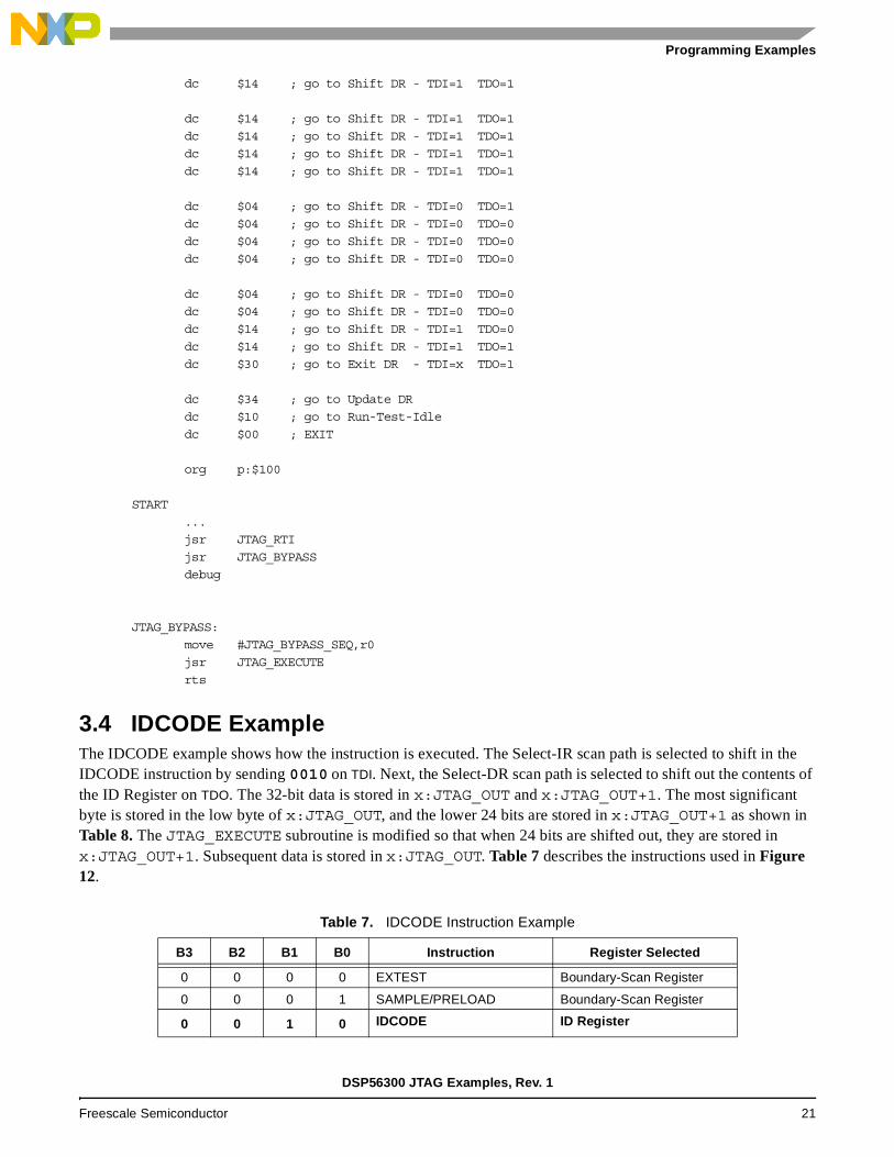
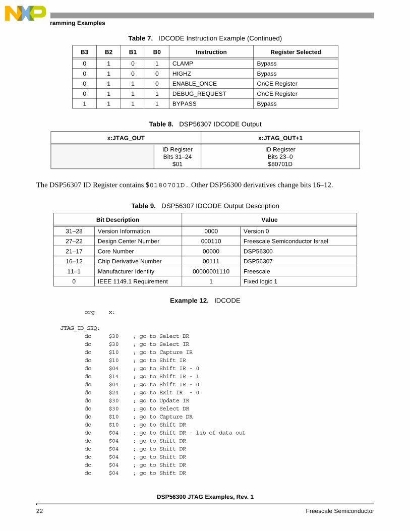
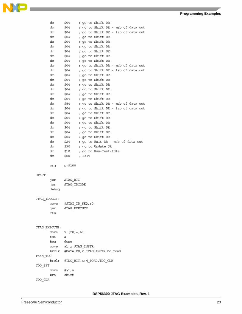
3.4 IDCODE ExampleThe IDCODE example shows how the instruction is executed. The Select-IR scan path is selected to shift in the IDCODE instruction by sending 0010 on TDI. Next, the Select-DR scan path is selected to shift out the contents of the ID Register on TDO. The 32-bit data is stored in x:JTAG_OUT and x:JTAG_OUT+1. The most significant byte is stored in the low byte of x:JTAG_OUT, and the lower 24 bits are stored in x:JTAG_OUT+1 as shown in Table 8. The JTAG_EXECUTE subroutine is modified so that when 24 bits are shifted out, they are stored in x:JTAG_OUT+1. Subsequent data is stored in x:JTAG_OUT. Table 7 describes the instructions used in Figure 12.
Table 7. IDCODE Instruction Example
B3 B2 B1 B0 Instruction Register Selected
0 0 0 0 EXTEST Boundary-Scan Register
0 0 0 1 SAMPLE/PRELOAD Boundary-Scan Register
0 0 1 0 IDCODE ID Register
DSP56300 JTAG Examples, Rev. 1
Freescale Semiconductor 21
Programming Examples
The DSP56307 ID Register contains $0180701D. Other DSP56300 derivatives change bits 16–12.
Example 12. IDCODE
org x:
JTAG_ID_SEQ:
dc $30 ; go to Select DR
dc $30 ; go to Select IR
dc $10 ; go to Capture IR
dc $10 ; go to Shift IR
dc $04 ; go to Shift IR - 0
dc $14 ; go to Shift IR - 1
dc $04 ; go to Shift IR - 0
dc $24 ; go to Exit IR - 0
dc $30 ; go to Update IR
dc $30 ; go to Select DR
dc $10 ; go to Capture DR
dc $10 ; go to Shift DR
dc $04 ; go to Shift DR - lsb of data out
dc $04 ; go to Shift DR
dc $04 ; go to Shift DR
dc $04 ; go to Shift DR
dc $04 ; go to Shift DR
dc $04 ; go to Shift DR
0 1 0 1 CLAMP Bypass
0 1 0 0 HIGHZ Bypass
0 1 1 0 ENABLE_ONCE OnCE Register
0 1 1 1 DEBUG_REQUEST OnCE Register
1 1 1 1 BYPASS Bypass
Table 8. DSP56307 IDCODE Output
x:JTAG_OUT x:JTAG_OUT+1
ID RegisterBits 31–24
$01
ID RegisterBits 23–0$80701D
Table 9. DSP56307 IDCODE Output Description
Bit Description Value
31–28 Version Information 0000 Version 0
27–22 Design Center Number 000110 Freescale Semiconductor Israel
21–17 Core Number 00000 DSP56300
16–12 Chip Derivative Number 00111 DSP56307
11–1 Manufacturer Identity 00000001110 Freescale
0 IEEE 1149.1 Requirement 1 Fixed logic 1
Table 7. IDCODE Instruction Example (Continued)
B3 B2 B1 B0 Instruction Register Selected
DSP56300 JTAG Examples, Rev. 1
22 Freescale Semiconductor
Programming Examples
dc $04 ; go to Shift DR
dc $04 ; go to Shift DR - msb of data out
dc $04 ; go to Shift DR - lsb of data out
dc $04 ; go to Shift DR
dc $04 ; go to Shift DR
dc $04 ; go to Shift DR
dc $04 ; go to Shift DR
dc $04 ; go to Shift DR
dc $04 ; go to Shift DR
dc $04 ; go to Shift DR - msb of data out
dc $04 ; go to Shift DR - lsb of data out
dc $04 ; go to Shift DR
dc $04 ; go to Shift DR
dc $04 ; go to Shift DR
dc $04 ; go to Shift DR
dc $04 ; go to Shift DR
dc $04 ; go to Shift DR
dc $84 ; go to Shift DR - msb of data out
dc $04 ; go to Shift DR - lsb of data out
dc $04 ; go to Shift DR
dc $04 ; go to Shift DR
dc $04 ; go to Shift DR
dc $04 ; go to Shift DR
dc $04 ; go to Shift DR
dc $04 ; go to Shift DR
dc $24 ; go to Exit DR - msb of data out
dc $30 ; go to Update DR
dc $10 ; go to Run-Test-Idle
dc $00 ; EXIT
org p:$100
START
jsr JTAG_RTI
jsr JTAG_IDCODE
debug
JTAG_IDCODE:
move #JTAG_ID_SEQ,r0
jsr JTAG_EXECUTE
rts
JTAG_EXECUTE:
move x:(r0)+,a1
tst a
beq done
move a1,x:JTAG_INSTR
brclr #DATA_RD,x:JTAG_INSTR,no_read
read_TDO
brclr #TDO_BIT,x:M_PDRD,TDO_CLR
TDO_SET
move #>1,a
bra shift
TDO_CLR
DSP56300 JTAG Examples, Rev. 1
Freescale Semiconductor 23
Programming Examples
move #>0,a
shift
lsr a
ror b
no_read
brclr #DATA_TMS,x:JTAG_INSTR,TMS_CLR
TMS_SET
bset #TMS_BIT,x:M_PDRD
bra >cont1
TMS_CLR
bclr #TMS_BIT,x:M_PDRD
cont1
brclr #DATA_TDI,x:JTAG_INSTR,TDI_CLR
TDI_SET
bset #TDI_BIT,x:M_PDRD
bra >cont2
TDI_CLR
bclr #TDI_BIT,x:M_PDRD
cont2
bset #TCK_BIT,x:M_PDRD
rep #3
nop
bclr #TCK_BIT,x:M_PDRD
brclr #COUNT24,x:JTAG_INSTR,not24bits
move b1,x:(r1)-
clr b
not24bits
bra >JTAG_EXECUTE
done
lsr #16,b
nop
move b1,x:(r1)-
clr b
rts
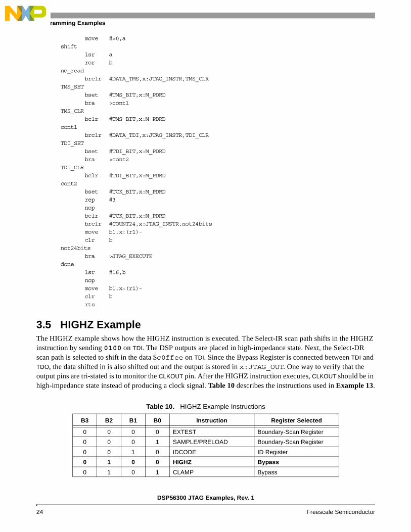
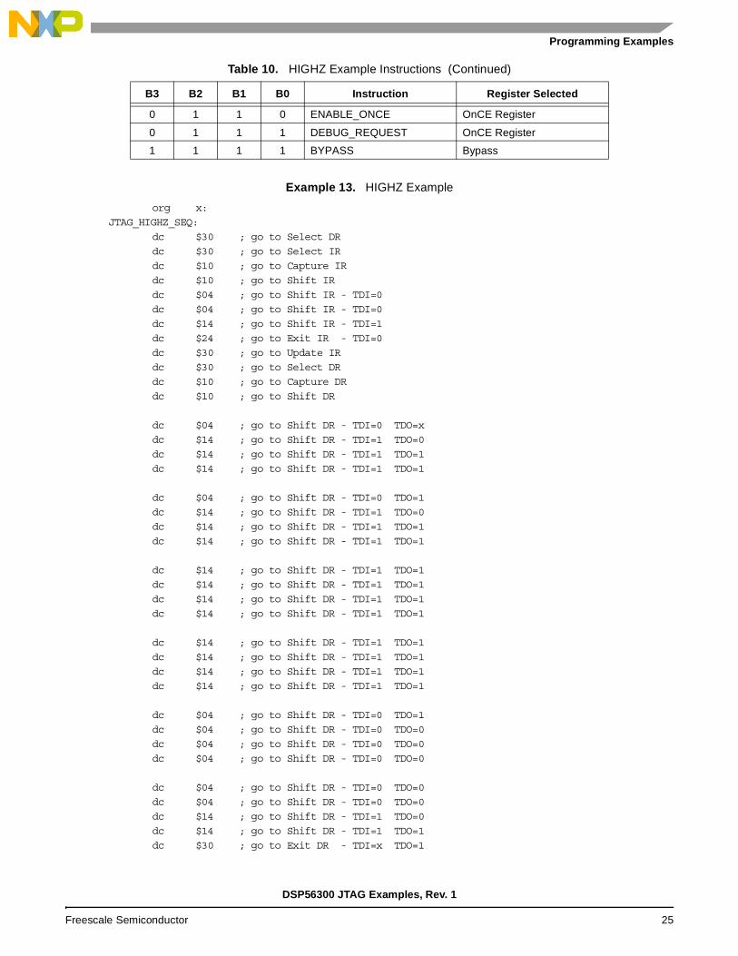
3.5 HIGHZ ExampleThe HIGHZ example shows how the HIGHZ instruction is executed. The Select-IR scan path shifts in the HIGHZ instruction by sending 0100 on TDI. The DSP outputs are placed in high-impedance state. Next, the Select-DR scan path is selected to shift in the data $c0ffee on TDI. Since the Bypass Register is connected between TDI and TDO, the data shifted in is also shifted out and the output is stored in x:JTAG_OUT. One way to verify that the output pins are tri-stated is to monitor the CLKOUT pin. After the HIGHZ instruction executes, CLKOUT should be in high-impedance state instead of producing a clock signal. Table 10 describes the instructions used in Example 13.
Table 10. HIGHZ Example Instructions
B3 B2 B1 B0 Instruction Register Selected
0 0 0 0 EXTEST Boundary-Scan Register
0 0 0 1 SAMPLE/PRELOAD Boundary-Scan Register
0 0 1 0 IDCODE ID Register
0 1 0 0 HIGHZ Bypass
0 1 0 1 CLAMP Bypass
DSP56300 JTAG Examples, Rev. 1
24 Freescale Semiconductor
Programming Examples
Example 13. HIGHZ Example
org x:
JTAG_HIGHZ_SEQ:
dc $30 ; go to Select DR
dc $30 ; go to Select IR
dc $10 ; go to Capture IR
dc $10 ; go to Shift IR
dc $04 ; go to Shift IR - TDI=0
dc $04 ; go to Shift IR - TDI=0
dc $14 ; go to Shift IR - TDI=1
dc $24 ; go to Exit IR - TDI=0
dc $30 ; go to Update IR
dc $30 ; go to Select DR
dc $10 ; go to Capture DR
dc $10 ; go to Shift DR
dc $04 ; go to Shift DR - TDI=0 TDO=x
dc $14 ; go to Shift DR - TDI=1 TDO=0
dc $14 ; go to Shift DR - TDI=1 TDO=1
dc $14 ; go to Shift DR - TDI=1 TDO=1
dc $04 ; go to Shift DR - TDI=0 TDO=1
dc $14 ; go to Shift DR - TDI=1 TDO=0
dc $14 ; go to Shift DR - TDI=1 TDO=1
dc $14 ; go to Shift DR - TDI=1 TDO=1
dc $14 ; go to Shift DR - TDI=1 TDO=1
dc $14 ; go to Shift DR - TDI=1 TDO=1
dc $14 ; go to Shift DR - TDI=1 TDO=1
dc $14 ; go to Shift DR - TDI=1 TDO=1
dc $14 ; go to Shift DR - TDI=1 TDO=1
dc $14 ; go to Shift DR - TDI=1 TDO=1
dc $14 ; go to Shift DR - TDI=1 TDO=1
dc $14 ; go to Shift DR - TDI=1 TDO=1
dc $04 ; go to Shift DR - TDI=0 TDO=1
dc $04 ; go to Shift DR - TDI=0 TDO=0
dc $04 ; go to Shift DR - TDI=0 TDO=0
dc $04 ; go to Shift DR - TDI=0 TDO=0
dc $04 ; go to Shift DR - TDI=0 TDO=0
dc $04 ; go to Shift DR - TDI=0 TDO=0
dc $14 ; go to Shift DR - TDI=1 TDO=0
dc $14 ; go to Shift DR - TDI=1 TDO=1
dc $30 ; go to Exit DR - TDI=x TDO=1
0 1 1 0 ENABLE_ONCE OnCE Register
0 1 1 1 DEBUG_REQUEST OnCE Register
1 1 1 1 BYPASS Bypass
Table 10. HIGHZ Example Instructions (Continued)
B3 B2 B1 B0 Instruction Register Selected
DSP56300 JTAG Examples, Rev. 1
Freescale Semiconductor 25
Programming Examples
dc $34 ; go to Update DR
dc $10 ; go to Run-Test-Idle
dc $00 ; EXIT
org p:$100
START
...
jsr JTAG_RTI
jsr JTAG_HIGHZ
debug
JTAG_HIGHZ:
move #JTAG_HIGHZ_SEQ,r0
jsr JTAG_EXECUTE
rts
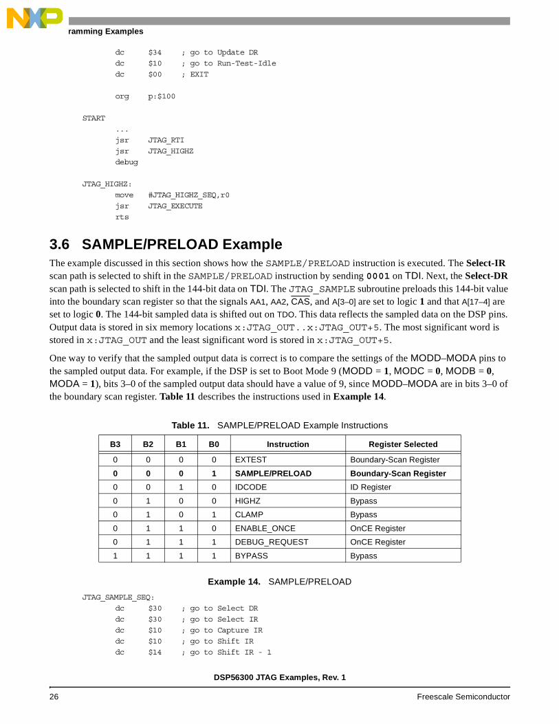
3.6 SAMPLE/PRELOAD ExampleThe example discussed in this section shows how the SAMPLE/PRELOAD instruction is executed. The Select-IR scan path is selected to shift in the SAMPLE/PRELOAD instruction by sending 0001 on TDI. Next, the Select-DR scan path is selected to shift in the 144-bit data on TDI. The JTAG_SAMPLE subroutine preloads this 144-bit value into the boundary scan register so that the signals AA1, AA2, CAS, and A[3–0] are set to logic 1 and that A[17–4] are set to logic 0. The 144-bit sampled data is shifted out on TDO. This data reflects the sampled data on the DSP pins. Output data is stored in six memory locations x:JTAG_OUT..x:JTAG_OUT+5. The most significant word is stored in x:JTAG_OUT and the least significant word is stored in x:JTAG_OUT+5.
One way to verify that the sampled output data is correct is to compare the settings of the MODD–MODA pins to the sampled output data. For example, if the DSP is set to Boot Mode 9 (MODD = 1, MODC = 0, MODB = 0, MODA = 1), bits 3–0 of the sampled output data should have a value of 9, since MODD–MODA are in bits 3–0 of the boundary scan register. Table 11 describes the instructions used in Example 14.
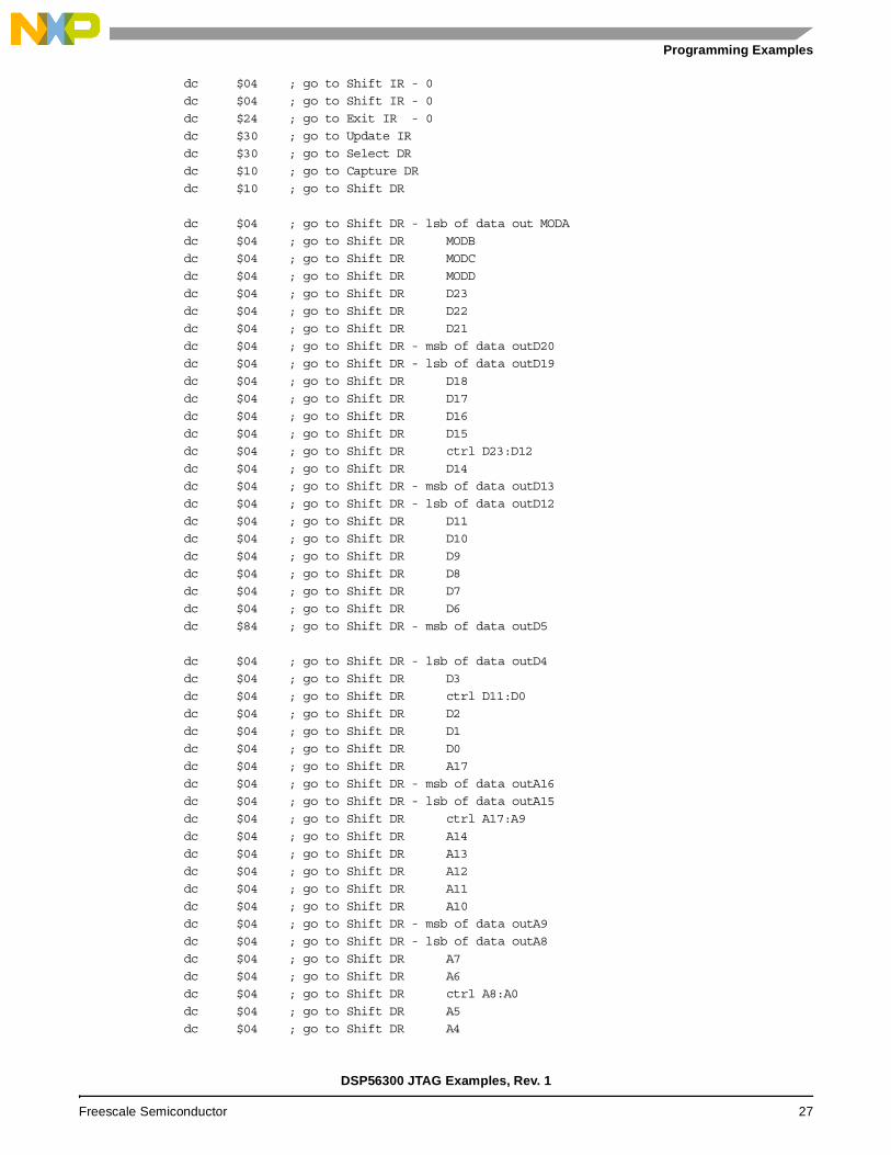
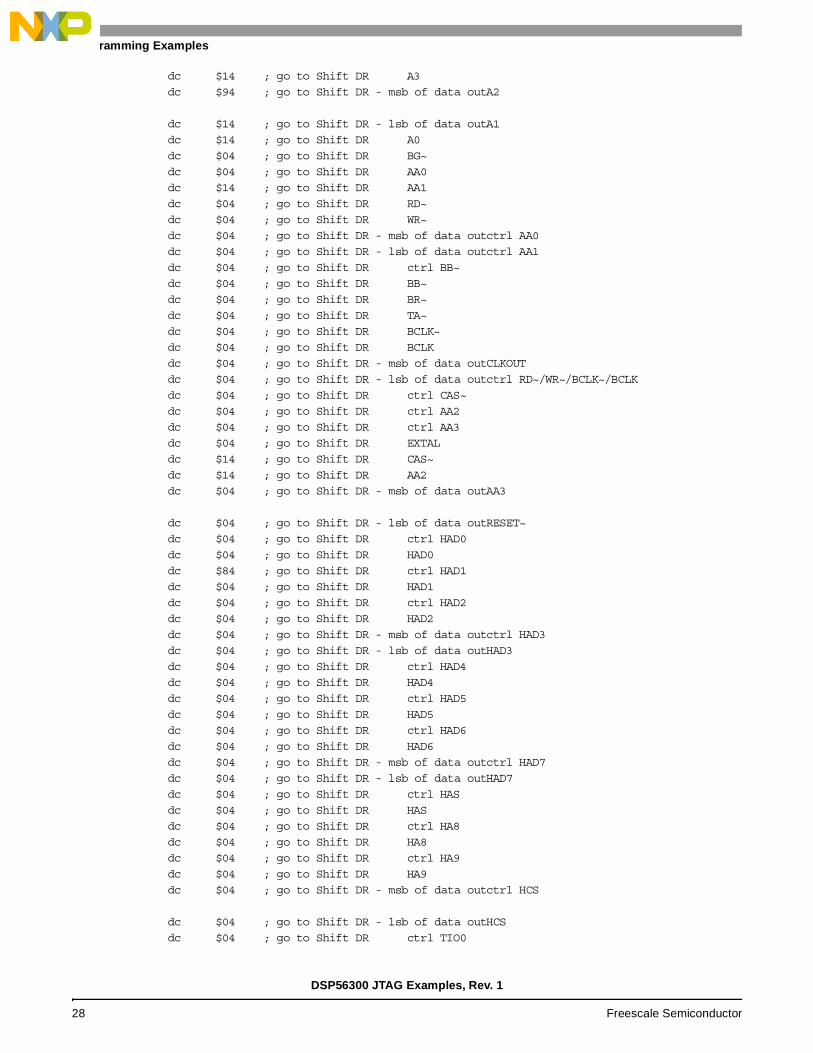
Example 14. SAMPLE/PRELOAD
JTAG_SAMPLE_SEQ:
dc $30 ; go to Select DR
dc $30 ; go to Select IR
dc $10 ; go to Capture IR
dc $10 ; go to Shift IR
dc $14 ; go to Shift IR - 1
Table 11. SAMPLE/PRELOAD Example Instructions
B3 B2 B1 B0 Instruction Register Selected
0 0 0 0 EXTEST Boundary-Scan Register
0 0 0 1 SAMPLE/PRELOAD Boundary-Scan Register
0 0 1 0 IDCODE ID Register
0 1 0 0 HIGHZ Bypass
0 1 0 1 CLAMP Bypass
0 1 1 0 ENABLE_ONCE OnCE Register
0 1 1 1 DEBUG_REQUEST OnCE Register
1 1 1 1 BYPASS Bypass
DSP56300 JTAG Examples, Rev. 1
26 Freescale Semiconductor
Programming Examples
dc $04 ; go to Shift IR - 0
dc $04 ; go to Shift IR - 0
dc $24 ; go to Exit IR - 0
dc $30 ; go to Update IR
dc $30 ; go to Select DR
dc $10 ; go to Capture DR
dc $10 ; go to Shift DR
dc $04 ; go to Shift DR - lsb of data out MODA
dc $04 ; go to Shift DR MODB
dc $04 ; go to Shift DR MODC
dc $04 ; go to Shift DR MODD
dc $04 ; go to Shift DR D23
dc $04 ; go to Shift DR D22
dc $04 ; go to Shift DR D21
dc $04 ; go to Shift DR - msb of data outD20
dc $04 ; go to Shift DR - lsb of data outD19
dc $04 ; go to Shift DR D18
dc $04 ; go to Shift DR D17
dc $04 ; go to Shift DR D16
dc $04 ; go to Shift DR D15
dc $04 ; go to Shift DR ctrl D23:D12
dc $04 ; go to Shift DR D14
dc $04 ; go to Shift DR - msb of data outD13
dc $04 ; go to Shift DR - lsb of data outD12
dc $04 ; go to Shift DR D11
dc $04 ; go to Shift DR D10
dc $04 ; go to Shift DR D9
dc $04 ; go to Shift DR D8
dc $04 ; go to Shift DR D7
dc $04 ; go to Shift DR D6
dc $84 ; go to Shift DR - msb of data outD5
dc $04 ; go to Shift DR - lsb of data outD4
dc $04 ; go to Shift DR D3
dc $04 ; go to Shift DR ctrl D11:D0
dc $04 ; go to Shift DR D2
dc $04 ; go to Shift DR D1
dc $04 ; go to Shift DR D0
dc $04 ; go to Shift DR A17
dc $04 ; go to Shift DR - msb of data outA16
dc $04 ; go to Shift DR - lsb of data outA15
dc $04 ; go to Shift DR ctrl A17:A9
dc $04 ; go to Shift DR A14
dc $04 ; go to Shift DR A13
dc $04 ; go to Shift DR A12
dc $04 ; go to Shift DR A11
dc $04 ; go to Shift DR A10
dc $04 ; go to Shift DR - msb of data outA9
dc $04 ; go to Shift DR - lsb of data outA8
dc $04 ; go to Shift DR A7
dc $04 ; go to Shift DR A6
dc $04 ; go to Shift DR ctrl A8:A0
dc $04 ; go to Shift DR A5
dc $04 ; go to Shift DR A4
DSP56300 JTAG Examples, Rev. 1
Freescale Semiconductor 27
Programming Examples
dc $14 ; go to Shift DR A3
dc $94 ; go to Shift DR - msb of data outA2
dc $14 ; go to Shift DR - lsb of data outA1
dc $14 ; go to Shift DR A0
dc $04 ; go to Shift DR BG~
dc $04 ; go to Shift DR AA0
dc $14 ; go to Shift DR AA1
dc $04 ; go to Shift DR RD~
dc $04 ; go to Shift DR WR~
dc $04 ; go to Shift DR - msb of data outctrl AA0
dc $04 ; go to Shift DR - lsb of data outctrl AA1
dc $04 ; go to Shift DR ctrl BB~
dc $04 ; go to Shift DR BB~
dc $04 ; go to Shift DR BR~
dc $04 ; go to Shift DR TA~
dc $04 ; go to Shift DR BCLK~
dc $04 ; go to Shift DR BCLK
dc $04 ; go to Shift DR - msb of data outCLKOUT
dc $04 ; go to Shift DR - lsb of data outctrl RD~/WR~/BCLK~/BCLK
dc $04 ; go to Shift DR ctrl CAS~
dc $04 ; go to Shift DR ctrl AA2
dc $04 ; go to Shift DR ctrl AA3
dc $04 ; go to Shift DR EXTAL
dc $14 ; go to Shift DR CAS~
dc $14 ; go to Shift DR AA2
dc $04 ; go to Shift DR - msb of data outAA3
dc $04 ; go to Shift DR - lsb of data outRESET~
dc $04 ; go to Shift DR ctrl HAD0
dc $04 ; go to Shift DR HAD0
dc $84 ; go to Shift DR ctrl HAD1
dc $04 ; go to Shift DR HAD1
dc $04 ; go to Shift DR ctrl HAD2
dc $04 ; go to Shift DR HAD2
dc $04 ; go to Shift DR - msb of data outctrl HAD3
dc $04 ; go to Shift DR - lsb of data outHAD3
dc $04 ; go to Shift DR ctrl HAD4
dc $04 ; go to Shift DR HAD4
dc $04 ; go to Shift DR ctrl HAD5
dc $04 ; go to Shift DR HAD5
dc $04 ; go to Shift DR ctrl HAD6
dc $04 ; go to Shift DR HAD6
dc $04 ; go to Shift DR - msb of data outctrl HAD7
dc $04 ; go to Shift DR - lsb of data outHAD7
dc $04 ; go to Shift DR ctrl HAS
dc $04 ; go to Shift DR HAS
dc $04 ; go to Shift DR ctrl HA8
dc $04 ; go to Shift DR HA8
dc $04 ; go to Shift DR ctrl HA9
dc $04 ; go to Shift DR HA9
dc $04 ; go to Shift DR - msb of data outctrl HCS
dc $04 ; go to Shift DR - lsb of data outHCS
dc $04 ; go to Shift DR ctrl TIO0
DSP56300 JTAG Examples, Rev. 1
28 Freescale Semiconductor
Programming Examples
dc $04 ; go to Shift DR TIO0
dc $84 ; go to Shift DR ctrl TIO1
dc $04 ; go to Shift DR TIO1
dc $04 ; go to Shift DR ctrl TIO2
dc $04 ; go to Shift DR TIO2
dc $04 ; go to Shift DR - msb of data outctrl HREQ
dc $04 ; go to Shift DR - lsb of data outHREQ
dc $04 ; go to Shift DR ctrl HACK
dc $04 ; go to Shift DR HACK
dc $04 ; go to Shift DR ctrl HRW
dc $04 ; go to Shift DR HRW
dc $04 ; go to Shift DR ctrl HDS
dc $04 ; go to Shift DR HDS
dc $04 ; go to Shift DR - msb of data outctrl SCK0
dc $04 ; go to Shift DR - lsb of data outSCK0
dc $04 ; go to Shift DR ctrl SCK1
dc $04 ; go to Shift DR SCK1
dc $04 ; go to Shift DR ctrl SCLK
dc $04 ; go to Shift DR SCLK
dc $04 ; go to Shift DR ctrl TXD
dc $04 ; go to Shift DR TXD
dc $04 ; go to Shift DR - msb of data outctrl RXD
dc $04 ; go to Shift DR - lsb of data outRXD
dc $04 ; go to Shift DR ctrl SC00
dc $04 ; go to Shift DR SC00
dc $84 ; go to Shift DR ctrl SC10
dc $04 ; go to Shift DR SC10
dc $04 ; go to Shift DR ctrl STD0
dc $04 ; go to Shift DR STD0
dc $04 ; go to Shift DR - msb of data outctrl SRD0
dc $04 ; go to Shift DR - lsb of data outSRD0
dc $04 ; go to Shift DR PINIT
dc $04 ; go to Shift DR ctrl DE~
dc $04 ; go to Shift DR DE~
dc $04 ; go to Shift DR ctrl SC01
dc $04 ; go to Shift DR SC01
dc $04 ; go to Shift DR ctrl SC02
dc $04 ; go to Shift DR - msb of data outSC02
dc $04 ; go to Shift DR - lsb of data outctrl STD1
dc $04 ; go to Shift DR STD1
dc $04 ; go to Shift DR ctrl SRD1
dc $04 ; go to Shift DR SRD1
dc $04 ; go to Shift DR ctrl SC11
dc $04 ; go to Shift DR SC11
dc $04 ; go to Shift DR ctrl SC12
dc $a4 ; go to Exit DR - msb of data outSC12
dc $30 ; go to Update DR
dc $10 ; go to Run-Test-Idle
dc $00 ; EXIT
org p:$100
START
...
jsr JTAG_RTI
DSP56300 JTAG Examples, Rev. 1
Freescale Semiconductor 29
Programming Examples
jsr JTAG_SAMPLE
debug
JTAG_SAMPLE:
move #JTAG_SAMPLE_SEQ,r0
jsr JTAG_EXECUTE
rts
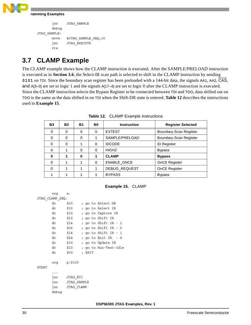
3.7 CLAMP ExampleThe CLAMP example shows how the CLAMP instruction is executed. After the SAMPLE/PRELOAD instruction is executed as in Section 3.6, the Select-IR scan path is selected to shift in the CLAMP instruction by sending 0101 on TDI. Since the boundary scan register has been preloaded with a 144-bit data, the signals AA1, AA2, CAS, and A[3–0] are set to logic 1 and the signals A[17–4] are set to logic 0 after the CLAMP instruction is executed. Since the CLAMP instruction selects the Bypass Register to be connected between TDI and TDO, data shifted out on TDO is the same as the data shifted in on TDI when the Shift-DR state is entered. Table 12 describes the instructions used in Example 15.
Example 15. CLAMP
org x:
JTAG_CLAMP_SEQ:
dc $30 ; go to Select DR
dc $30 ; go to Select IR
dc $10 ; go to Capture IR
dc $10 ; go to Shift IR
dc $14 ; go to Shift IR - 1
dc $04 ; go to Shift IR - 0
dc $14 ; go to Shift IR - 1
dc $24 ; go to Exit IR - 0
dc $30 ; go to Update IR
dc $10 ; go to Run-Test-Idle
dc $00 ; EXIT
org p:$100
START
...
jsr JTAG_RTI
jsr JTAG_SAMPLE
jsr JTAG_CLAMP
debug
Table 12. CLAMP Example Instructions
B3 B2 B1 B0 Instruction Register Selected
0 0 0 0 EXTEST Boundary-Scan Register
0 0 0 1 SAMPLE/PRELOAD Boundary-Scan Register
0 0 1 0 IDCODE ID Register
0 1 0 0 HIGHZ Bypass
0 1 0 1 CLAMP Bypass
0 1 1 0 ENABLE_ONCE OnCE Register
0 1 1 1 DEBUG_REQUEST OnCE Register
1 1 1 1 BYPASS Bypass
DSP56300 JTAG Examples, Rev. 1
30 Freescale Semiconductor
Programming Examples
JTAG_CLAMP:
move #JTAG_CLAMP_SEQ,r0
jsr JTAG_EXECUTE
rts
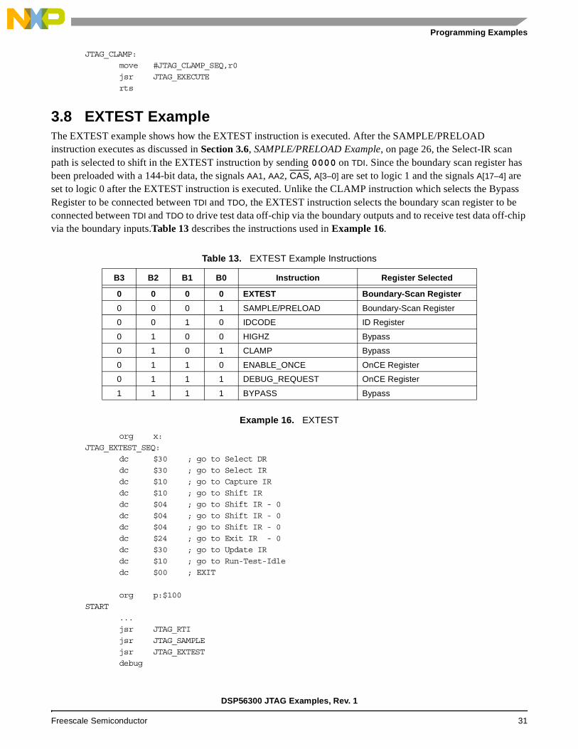
3.8 EXTEST ExampleThe EXTEST example shows how the EXTEST instruction is executed. After the SAMPLE/PRELOAD instruction executes as discussed in Section 3.6, SAMPLE/PRELOAD Example, on page 26, the Select-IR scan path is selected to shift in the EXTEST instruction by sending 0000 on TDI. Since the boundary scan register has been preloaded with a 144-bit data, the signals AA1, AA2, CAS, A[3–0] are set to logic 1 and the signals A[17–4] are set to logic 0 after the EXTEST instruction is executed. Unlike the CLAMP instruction which selects the Bypass Register to be connected between TDI and TDO, the EXTEST instruction selects the boundary scan register to be connected between TDI and TDO to drive test data off-chip via the boundary outputs and to receive test data off-chip via the boundary inputs.Table 13 describes the instructions used in Example 16.
Example 16. EXTEST
org x:
JTAG_EXTEST_SEQ:
dc $30 ; go to Select DR
dc $30 ; go to Select IR
dc $10 ; go to Capture IR
dc $10 ; go to Shift IR
dc $04 ; go to Shift IR - 0
dc $04 ; go to Shift IR - 0
dc $04 ; go to Shift IR - 0
dc $24 ; go to Exit IR - 0
dc $30 ; go to Update IR
dc $10 ; go to Run-Test-Idle
dc $00 ; EXIT
org p:$100
START
...
jsr JTAG_RTI
jsr JTAG_SAMPLE
jsr JTAG_EXTEST
debug
Table 13. EXTEST Example Instructions
B3 B2 B1 B0 Instruction Register Selected
0 0 0 0 EXTEST Boundary-Scan Register
0 0 0 1 SAMPLE/PRELOAD Boundary-Scan Register
0 0 1 0 IDCODE ID Register
0 1 0 0 HIGHZ Bypass
0 1 0 1 CLAMP Bypass
0 1 1 0 ENABLE_ONCE OnCE Register
0 1 1 1 DEBUG_REQUEST OnCE Register
1 1 1 1 BYPASS Bypass
DSP56300 JTAG Examples, Rev. 1
Freescale Semiconductor 31
Programming Examples
JTAG_EXTEST:
move #JTAG_EXTEST_SEQ,r0
jsr JTAG_EXECUTE
rts
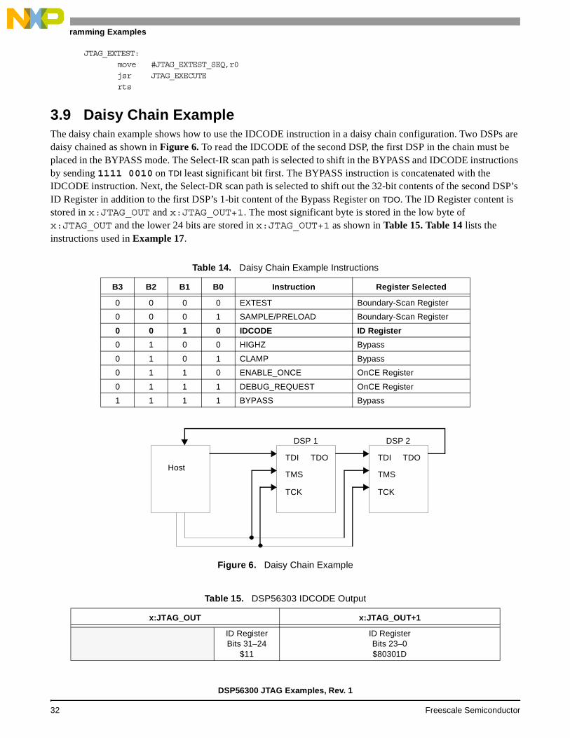
3.9 Daisy Chain ExampleThe daisy chain example shows how to use the IDCODE instruction in a daisy chain configuration. Two DSPs are daisy chained as shown in Figure 6. To read the IDCODE of the second DSP, the first DSP in the chain must be placed in the BYPASS mode. The Select-IR scan path is selected to shift in the BYPASS and IDCODE instructions by sending 1111 0010 on TDI least significant bit first. The BYPASS instruction is concatenated with the IDCODE instruction. Next, the Select-DR scan path is selected to shift out the 32-bit contents of the second DSP’s ID Register in addition to the first DSP’s 1-bit content of the Bypass Register on TDO. The ID Register content is stored in x:JTAG_OUT and x:JTAG_OUT+1. The most significant byte is stored in the low byte of x:JTAG_OUT and the lower 24 bits are stored in x:JTAG_OUT+1 as shown in Table 15. Table 14 lists the instructions used in Example 17.
Figure 6. Daisy Chain Example
Table 14. Daisy Chain Example Instructions
B3 B2 B1 B0 Instruction Register Selected
0 0 0 0 EXTEST Boundary-Scan Register
0 0 0 1 SAMPLE/PRELOAD Boundary-Scan Register
0 0 1 0 IDCODE ID Register
0 1 0 0 HIGHZ Bypass
0 1 0 1 CLAMP Bypass
0 1 1 0 ENABLE_ONCE OnCE Register
0 1 1 1 DEBUG_REQUEST OnCE Register
1 1 1 1 BYPASS Bypass
Table 15. DSP56303 IDCODE Output
x:JTAG_OUT x:JTAG_OUT+1
ID RegisterBits 31–24
$11
ID RegisterBits 23–0$80301D
TDI TDO
TMS
TCK
TDI TDO
TMS
TCK
DSP 1 DSP 2
Host
DSP56300 JTAG Examples, Rev. 1
32 Freescale Semiconductor
Programming Examples
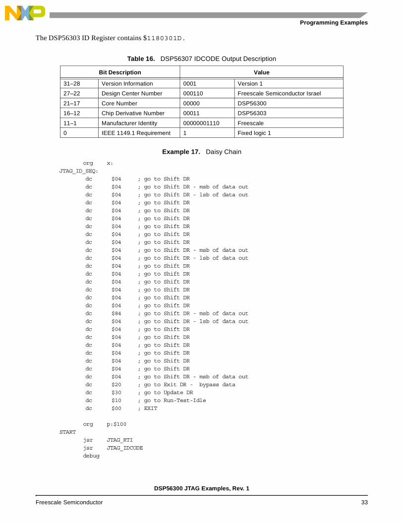
The DSP56303 ID Register contains $1180301D.
Example 17. Daisy Chain
org x:
JTAG_ID_SEQ:
dc $04 ; go to Shift DR
dc $04 ; go to Shift DR - msb of data out
dc $04 ; go to Shift DR - lsb of data out
dc $04 ; go to Shift DR
dc $04 ; go to Shift DR
dc $04 ; go to Shift DR
dc $04 ; go to Shift DR
dc $04 ; go to Shift DR
dc $04 ; go to Shift DR
dc $04 ; go to Shift DR - msb of data out
dc $04 ; go to Shift DR - lsb of data out
dc $04 ; go to Shift DR
dc $04 ; go to Shift DR
dc $04 ; go to Shift DR
dc $04 ; go to Shift DR
dc $04 ; go to Shift DR
dc $04 ; go to Shift DR
dc $84 ; go to Shift DR - msb of data out
dc $04 ; go to Shift DR - lsb of data out
dc $04 ; go to Shift DR
dc $04 ; go to Shift DR
dc $04 ; go to Shift DR
dc $04 ; go to Shift DR
dc $04 ; go to Shift DR
dc $04 ; go to Shift DR
dc $04 ; go to Shift DR - msb of data out
dc $20 ; go to Exit DR - bypass data
dc $30 ; go to Update DR
dc $10 ; go to Run-Test-Idle
dc $00 ; EXIT
org p:$100
START
jsr JTAG_RTI
jsr JTAG_IDCODE
debug
Table 16. DSP56307 IDCODE Output Description
Bit Description Value
31–28 Version Information 0001 Version 1
27–22 Design Center Number 000110 Freescale Semiconductor Israel
21–17 Core Number 00000 DSP56300
16–12 Chip Derivative Number 00011 DSP56303
11–1 Manufacturer Identity 00000001110 Freescale
0 IEEE 1149.1 Requirement 1 Fixed logic 1
DSP56300 JTAG Examples, Rev. 1
Freescale Semiconductor 33

Programming Examples
JTAG_IDCODE:
move #JTAG_ID_SEQ,r0
jsr JTAG_EXECUTE
rts
DSP56300 JTAG Examples, Rev. 1
34 Freescale Semiconductor

Programming Examples
NOTES:
DSP56300 JTAG Examples, Rev. 1
Freescale Semiconductor 35
Document Order No.: AN2074
Information in this document is provided solely to enable system and software implementers to use Freescale Semiconductor products. There are no express or implied copyright licenses granted hereunder to design or fabricate any integrated circuits or integrated circuits based on the information in this document.
Freescale Semiconductor reserves the right to make changes without further notice to any products herein. Freescale Semiconductor makes no warranty, representation or guarantee regarding the suitability of its products for any particular purpose, nor does Freescale Semiconductor assume any liability arising out of the application or use of any product or circuit, and specifically disclaims any and all liability, including without limitation consequential or incidental damages. “Typical” parameters which may be provided in Freescale Semiconductor data sheets and/or specifications can and do vary in different applications and actual performance may vary over time. All operating parameters, including “Typicals” must be validated for each customer application by customer’s technical experts. Freescale Semiconductor does not convey any license under its patent rights nor the rights of others. Freescale Semiconductor products are not designed, intended, or authorized for use as components in systems intended for surgical implant into the body, or other applications intended to support or sustain life, or for any other application in which the failure of the Freescale Semiconductor product could create a situation where personal injury or death may occur. Should Buyer purchase or use Freescale Semiconductor products for any such unintended or unauthorized application, Buyer shall indemnify and hold Freescale Semiconductor and its officers, employees, subsidiaries, affiliates, and distributors harmless against all claims, costs, damages, and expenses, and reasonable attorney fees arising out of, directly or indirectly, any claim of personal injury or death associated with such unintended or unauthorized use, even if such claim alleges that Freescale Semiconductor was negligent regarding the design or manufacture of the part.
Freescale™ and the Freescale logo are trademarks of Freescale Semiconductor, Inc. All other product or service names are the property of their respective owners.
© Freescale Semiconductor, Inc. 2000, 2005.
How to Reach Us:Home Page:www.freescale.com
E-mail:[email protected]
USA/Europe or Locations not listed:Freescale Semiconductor Technical Information Center, CH3701300 N. Alma School RoadChandler, Arizona 85224+1-800-521-6274 or [email protected]
Europe, Middle East, and Africa:Freescale Halbleiter Deutschland GMBHTechnical Information CenterSchatzbogen 781829 München, Germany+44 1296 380 456 (English)+46 8 52200080 (English)+49 89 92103 559 (German)+33 1 69 35 48 48 (French)[email protected]
Japan:Freescale Semiconductor Japan Ltd. HeadquartersARCO Tower 15F1-8-1, Shimo-Meguro, Meguro-ku,Tokyo 153-0064, Japan0120 191014 or +81 3 5437 [email protected]
Asia/Pacific:Freescale Semiconductor Hong Kong Ltd.Technical Information Center2 Dai King StreetTai Po Industrial EstateTai Po, N.T. Hong Kong+800 2666 8080
For Literature Requests Only:Freescale Semiconductor Literature Distribution CenterP.O. Box 5405Denver, Colorado 802171-800-441-2447 or 303-675-2140Fax: [email protected]
Rev. 18/2005