Embed Size (px)
Citation preview
PSoC® 4: PSoC 4100S Datasheet
Programmable System-on-Chip (PSoC)
Cypress Semiconductor Corporation • 198 Champion Court • San Jose, CA 95134-1709 • 408-943-2600Document Number: 002-00122 Rev. *K Revised April 3, 2018
General DescriptionPSoC® 4 is a scalable and reconfigurable platform architecture for a family of programmable embedded system controllers with anARM® Cortex™-M0+ CPU. It combines programmable and reconfigurable analog and digital blocks with flexible automatic routing.The PSoC 4100S product family is a member of the PSoC 4 platform architecture. It is a combination of a microcontroller with standardcommunication and timing peripherals, a capacitive touch-sensing system (CapSense) with best-in-class performance, programmablegeneral-purpose continuous-time and switched-capacitor analog blocks, and programmable connectivity. PSoC 4100S products willbe upward compatible with members of the PSoC 4 platform for new applications and design needs.
Features32-bit MCU Subsystem
48-MHz ARM Cortex-M0+ CPU
Up to 64 KB of flash with Read Accelerator
Up to 8 KB of SRAM
Programmable Analog
Two opamps with reconfigurable high-drive external and high-bandwidth internal drive and Comparator modes and ADC input buffering capability. Opamps can operate in Deep Sleep low-power mode.
12-bit 1-Msps SAR ADC with differential and single-ended modes, and Channel Sequencer with signal averaging
Single-slope 10-bit ADC function provided by a capacitance sensing block
Two current DACs (IDACs) for general-purpose or capacitive sensing applications on any pin
Two low-power comparators that operate in Deep Sleep low-power mode
Programmable Digital
Programmable logic blocks allowing Boolean operations to be performed on port inputs and outputs
Low-Power 1.71-V to 5.5-V Operation
Deep Sleep mode with operational analog and 2.5-A digital system current
Capacitive Sensing
Cypress CapSense Sigma-Delta (CSD) provides best-in-class signal-to-noise ratio (SNR) (>5:1) and water tolerance
Cypress-supplied software component makes capacitive sensing design easy
Automatic hardware tuning (SmartSense™)
LCD Drive Capability
LCD segment drive capability on GPIOs
Serial Communication
Three independent run-time reconfigurable Serial Communication Blocks (SCBs) with re-configurable I2C, SPI, or UART functionality
Timing and Pulse-Width Modulation
Five 16-bit timer/counter/pulse-width modulator (TCPWM) blocks
Center-aligned, Edge, and Pseudo-random modes
Comparator-based triggering of Kill signals for motor drive and other high-reliability digital logic applications
Quadrature decoder
Up to 36 Programmable GPIO Pins
48-pin TQFP, 44-pin TQFP, 40-pin QFN, 32-pin QFN, and 35-ball WLCSP packages
Any GPIO pin can be CapSense, analog, or digital
Drive modes, strengths, and slew rates are programmable
Clock Sources
32-kHz Watch Crystal Oscillator (WCO)
±2% Internal Main Oscillator (IMO)
32-kHz Internal Low-power Oscillator (ILO)
PSoC Creator Design Environment
Integrated Development Environment (IDE) provides schematic design entry and build (with analog and digital automatic routing)
Applications Programming Interface (API) component for all fixed-function and programmable peripherals
Industry-Standard Tool Compatibility
After schematic entry, development can be done with ARM-based industry-standard development tools
Document Number: 002-00122 Rev. *K Page 2 of 41
PSoC® 4: PSoC 4100S Datasheet
Development Support
Cypress provides a wealth of data at www.cypress.com to help you to select the right PSoC device for your design, and to help youto quickly and effectively integrate the device into your design. For a comprehensive list of resources, see the knowledge base articleKBA86521, How to Design with PSoC 3, PSoC 4, and PSoC 5LP. Following is an abbreviated list for PSoC 4:
Overview: PSoC Portfolio, PSoC Roadmap
Product Selectors: PSoC 1, PSoC 3, PSoC 4, PSoC 5LPIn addition, PSoC Creator includes a device selection tool.
Application notes: Cypress offers a large number of PSoC application notes covering a broad range of topics, from basic to advanced level. Recommended application notes for getting started with PSoC 4 are: AN79953: Getting Started With PSoC 4 AN88619: PSoC 4 Hardware Design Considerations AN86439: Using PSoC 4 GPIO Pins AN57821: Mixed Signal Circuit Board Layout AN81623: Digital Design Best Practices AN73854: Introduction To Bootloaders AN89610: ARM Cortex Code Optimization AN85951: PSoC® 4 and PSoC Analog Coprocessor
CapSense® Design Guide
Technical Reference Manual (TRM) is in two documents: Architecture TRM details each PSoC 4 functional block. Registers TRM describes each of the PSoC 4 registers.
Development Kits: CY8CKIT-041-41XX PSoC 4100S CapSense Pioneer Kit, is
an easy-to-use and inexpensive development platform. This kit includes connectors for Arduino™ compatible shields.
The MiniProg3 device provides an interface for flash programming and debug.
Software User Guide: A step-by-step guide for using PSoC Creator. The software
user guide shows you how the PSoC Creator build process works in detail, how to use source control with PSoC Creator, and much more.
Component Datasheets: The flexibility of PSoC allows the creation of new peripherals
(components) long after the device has gone into production. Component datasheets provide all the information needed to select and use a particular component, including a functional description, API documentation, example code, and AC/DC specifications.
Online:
In addition to print documentation, the Cypress PSoC forumsconnect you with fellow PSoC users and experts in PSoC fromaround the world, 24 hours a day, 7 days a week.
Document Number: 002-00122 Rev. *K Page 3 of 41
PSoC® 4: PSoC 4100S Datasheet
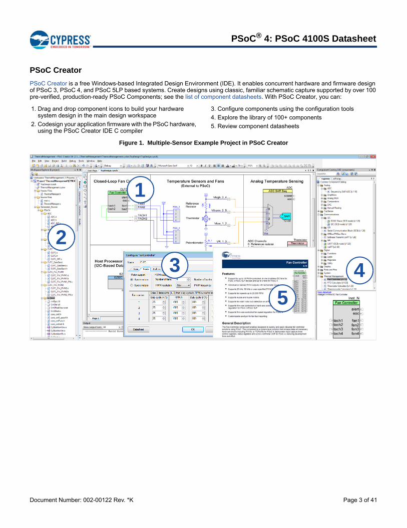
PSoC Creator
PSoC Creator is a free Windows-based Integrated Design Environment (IDE). It enables concurrent hardware and firmware design of PSoC 3, PSoC 4, and PSoC 5LP based systems. Create designs using classic, familiar schematic capture supported by over 100 pre-verified, production-ready PSoC Components; see the list of component datasheets. With PSoC Creator, you can:
1. Drag and drop component icons to build your hardware system design in the main design workspace
2. Codesign your application firmware with the PSoC hardware, using the PSoC Creator IDE C compiler
3. Configure components using the configuration tools
4. Explore the library of 100+ components
5. Review component datasheets
Figure 1. Multiple-Sensor Example Project in PSoC Creator
3
1
2
45

Document Number: 002-00122 Rev. *K Page 4 of 41
PSoC® 4: PSoC 4100S Datasheet
Contents
Functional Definition ........................................................ 6CPU and Memory Subsystem ..................................... 6System Resources ...................................................... 6Analog Blocks .............................................................. 7Programmable Digital Blocks ...................................... 7Fixed Function Digital .................................................. 7GPIO ........................................................................... 8Special Function Peripherals ....................................... 8
Pinouts .............................................................................. 9Alternate Pin Functions ............................................. 11
Power ............................................................................... 13Mode 1: 1.8 V to 5.5 V External Supply .................... 13Mode 2: 1.8 V ±5% External Supply .......................... 13
Electrical Specifications ................................................ 14Absolute Maximum Ratings ...................................... 14Device Level Specifications ....................................... 14Analog Peripherals .................................................... 18
Digital Peripherals ..................................................... 25Memory ..................................................................... 27System Resources .................................................... 27
Ordering Information ...................................................... 30Packaging ........................................................................ 32
Package Diagrams .................................................... 33Acronyms ........................................................................ 37Document Conventions ................................................. 39
Units of Measure ....................................................... 39Revision History ............................................................. 40Sales, Solutions, and Legal Information ...................... 41
Worldwide Sales and Design Support ....................... 41Products .................................................................... 41PSoC® Solutions ...................................................... 41Cypress Developer Community ................................. 41Technical Support ..................................................... 41

Document Number: 002-00122 Rev. *K Page 5 of 41
PSoC® 4: PSoC 4100S Datasheet
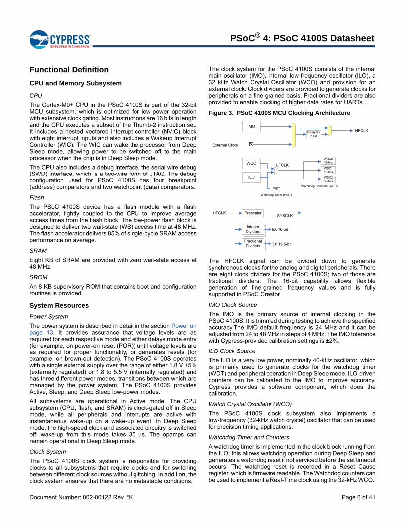
Figure 2. Block Diagram
PSoC 4100S devices include extensive support forprogramming, testing, debugging, and tracing both hardwareand firmware.
The ARM Serial-Wire Debug (SWD) interface supports allprogramming and debug features of the device.
Complete debug-on-chip functionality enables full-devicedebugging in the final system using the standard productiondevice. It does not require special interfaces, debugging pods,simulators, or emulators. Only the standard programmingconnections are required to fully support debug.
The PSoC Creator IDE provides fully integrated programmingand debug support for the PSoC 4100S devices. The SWDinterface is fully compatible with industry-standard third-partytools. The PSoC 4100S provides a level of security not possiblewith multi-chip application solutions or with microcontrollers.
It has the following advantages:
Allows disabling of debug features
Robust flash protection
Allows customer-proprietary functionality to be implemented in on-chip programmable blocks
The debug circuits are enabled by default and can be disabledin firmware. If they are not enabled, the only way to re-enablethem is to erase the entire device, clear flash protection, andreprogram the device with new firmware that enables debugging.Thus firmware control of debugging cannot be over-riddenwithout erasing the firmware thus providing security.
Additionally, all device interfaces can be permanently disabled(device security) for applications concerned about phishingattacks due to a maliciously reprogrammed device or attempts todefeat security by starting and interrupting flash programmingsequences. All programming, debug, and test interfaces aredisabled when maximum device security is enabled. Therefore,PSoC 4100S, with device security enabled, may not be returnedfor failure analysis. This is a trade-off the PSoC 4100S allows thecustomer to make.
Peripherals
CPU Subsystem
System Interconnect (Single Layer AHB)
PSoC 4100S Architecture
IOS
S G
PIO
(5x
por
ts)
I/O Subsystem
Peripheral Interconnect (MMIO)PCLK
SWD/TC
NVIC, IRQMUX
CortexM0+
48 MHzFAST MUL
FLASH64 KB
Read Accelerator
SPCIF
SRAM4 KB
SRAM Controller
ROM8 KB
ROM Controller
32-bit
AHB- Lite
2x S
CB
-I2
C/S
PI/
UA
RT
36x GPIOs, LCDDeepSleep
Active/ SleepPower Modes
Digital DFT
Test
Analog DFT
System ResourcesLite
Power
Clock
Reset
Clock Control
IMO
Sleep Control
REFPOR
Reset Control
TestMode Entry
WIC
XRES
WDTILO
PWRSYS
5x T
CP
WM
Ca
pS
ens
e
WC
O
2x L
P C
om
para
tor
SAR ADC(12-bit)
x1
CTBmx12x Opamp
ProgrammableAnalog
SARMUX
High Speed I/O Matrix & 2 x Programmable I/O
Document Number: 002-00122 Rev. *K Page 6 of 41
PSoC® 4: PSoC 4100S Datasheet
Functional Definition
CPU and Memory Subsystem
CPU
The Cortex-M0+ CPU in the PSoC 4100S is part of the 32-bitMCU subsystem, which is optimized for low-power operationwith extensive clock gating. Most instructions are 16 bits in lengthand the CPU executes a subset of the Thumb-2 instruction set.It includes a nested vectored interrupt controller (NVIC) blockwith eight interrupt inputs and also includes a Wakeup InterruptController (WIC). The WIC can wake the processor from DeepSleep mode, allowing power to be switched off to the mainprocessor when the chip is in Deep Sleep mode.
The CPU also includes a debug interface, the serial wire debug(SWD) interface, which is a two-wire form of JTAG. The debugconfiguration used for PSoC 4100S has four breakpoint(address) comparators and two watchpoint (data) comparators.
Flash
The PSoC 4100S device has a flash module with a flashaccelerator, tightly coupled to the CPU to improve averageaccess times from the flash block. The low-power flash block isdesigned to deliver two wait-state (WS) access time at 48 MHz.The flash accelerator delivers 85% of single-cycle SRAM accessperformance on average.
SRAM
Eight KB of SRAM are provided with zero wait-state access at48 MHz.
SROM
An 8 KB supervisory ROM that contains boot and configurationroutines is provided.
System Resources
Power System
The power system is described in detail in the section Power onpage 13. It provides assurance that voltage levels are asrequired for each respective mode and either delays mode entry(for example, on power-on reset (POR)) until voltage levels areas required for proper functionality, or generates resets (forexample, on brown-out detection). The PSoC 4100S operateswith a single external supply over the range of either 1.8 V ±5%(externally regulated) or 1.8 to 5.5 V (internally regulated) andhas three different power modes, transitions between which aremanaged by the power system. The PSoC 4100S providesActive, Sleep, and Deep Sleep low-power modes.
All subsystems are operational in Active mode. The CPUsubsystem (CPU, flash, and SRAM) is clock-gated off in Sleepmode, while all peripherals and interrupts are active withinstantaneous wake-up on a wake-up event. In Deep Sleepmode, the high-speed clock and associated circuitry is switchedoff; wake-up from this mode takes 35 µs. The opamps canremain operational in Deep Sleep mode.
Clock System
The PSoC 4100S clock system is responsible for providingclocks to all subsystems that require clocks and for switchingbetween different clock sources without glitching. In addition, theclock system ensures that there are no metastable conditions.
The clock system for the PSoC 4100S consists of the internalmain oscillator (IMO), internal low-frequency oscillator (ILO), a32 kHz Watch Crystal Oscillator (WCO) and provision for anexternal clock. Clock dividers are provided to generate clocks forperipherals on a fine-grained basis. Fractional dividers are alsoprovided to enable clocking of higher data rates for UARTs.
Figure 3. PSoC 4100S MCU Clocking Architecture
The HFCLK signal can be divided down to generatesynchronous clocks for the analog and digital peripherals. Thereare eight clock dividers for the PSoC 4100S; two of those arefractional dividers. The 16-bit capability allows flexiblegeneration of fine-grained frequency values and is fullysupported in PSoC Creator
IMO Clock Source
The IMO is the primary source of internal clocking in thePSoC 4100S. It is trimmed during testing to achieve the specifiedaccuracy.The IMO default frequency is 24 MHz and it can beadjusted from 24 to 48 MHz in steps of 4 MHz. The IMO tolerancewith Cypress-provided calibration settings is ±2%.
ILO Clock Source
The ILO is a very low power, nominally 40-kHz oscillator, whichis primarily used to generate clocks for the watchdog timer(WDT) and peripheral operation in Deep Sleep mode. ILO-drivencounters can be calibrated to the IMO to improve accuracy.Cypress provides a software component, which does thecalibration.
Watch Crystal Oscillator (WCO)
The PSoC 4100S clock subsystem also implements alow-frequency (32-kHz watch crystal) oscillator that can be usedfor precision timing applications.
Watchdog Timer and Counters
A watchdog timer is implemented in the clock block running fromthe ILO; this allows watchdog operation during Deep Sleep andgenerates a watchdog reset if not serviced before the set timeoutoccurs. The watchdog reset is recorded in a Reset Causeregister, which is firmware readable. The Watchdog counters canbe used to implement a Real-Time clock using the 32-kHz WCO.
IMO
External Clock
HFCLKDivide By2,4,8
3X 16.5-bit
Integer Dividers
FractionalDividers
SYSCLKPrescalerHFCLK
6X 16-bit
LFCLK
ILO
WCO
Watchdog Counters (WDC)WDT
Watchdog Timer (WDT)
WDC0 16-bits
WDC116-bits
WDC232-bits
Document Number: 002-00122 Rev. *K Page 7 of 41
PSoC® 4: PSoC 4100S Datasheet
Reset
The PSoC 4100S can be reset from a variety of sourcesincluding a software reset. Reset events are asynchronous andguarantee reversion to a known state. The reset cause isrecorded in a register, which is sticky through reset and allowssoftware to determine the cause of the reset. An XRES pin isreserved for external reset by asserting it active low. The XRESpin has an internal pull-up resistor that is always enabled.
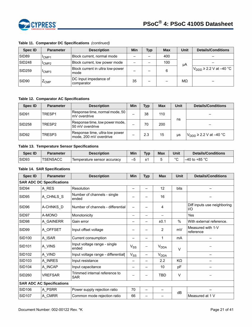
Analog Blocks
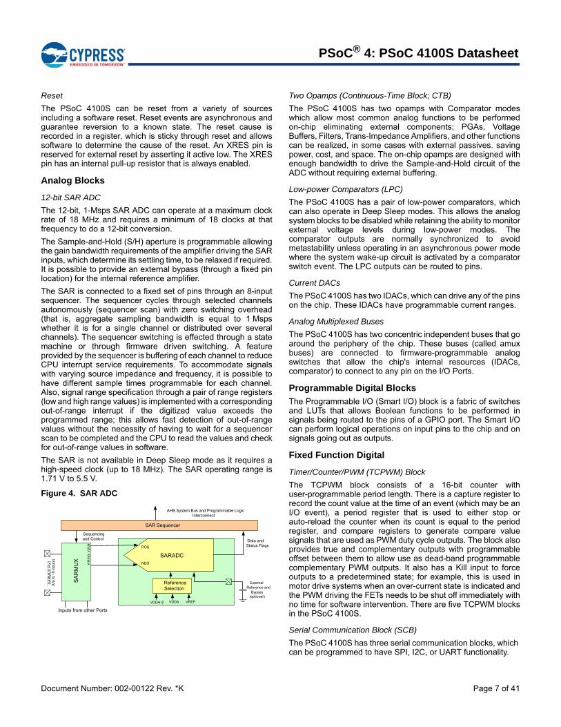
12-bit SAR ADC
The 12-bit, 1-Msps SAR ADC can operate at a maximum clockrate of 18 MHz and requires a minimum of 18 clocks at thatfrequency to do a 12-bit conversion.
The Sample-and-Hold (S/H) aperture is programmable allowingthe gain bandwidth requirements of the amplifier driving the SARinputs, which determine its settling time, to be relaxed if required.It is possible to provide an external bypass (through a fixed pinlocation) for the internal reference amplifier.
The SAR is connected to a fixed set of pins through an 8-inputsequencer. The sequencer cycles through selected channelsautonomously (sequencer scan) with zero switching overhead(that is, aggregate sampling bandwidth is equal to 1 Mspswhether it is for a single channel or distributed over severalchannels). The sequencer switching is effected through a statemachine or through firmware driven switching. A featureprovided by the sequencer is buffering of each channel to reduceCPU interrupt service requirements. To accommodate signalswith varying source impedance and frequency, it is possible tohave different sample times programmable for each channel.Also, signal range specification through a pair of range registers(low and high range values) is implemented with a correspondingout-of-range interrupt if the digitized value exceeds theprogrammed range; this allows fast detection of out-of-rangevalues without the necessity of having to wait for a sequencerscan to be completed and the CPU to read the values and checkfor out-of-range values in software.
The SAR is not available in Deep Sleep mode as it requires ahigh-speed clock (up to 18 MHz). The SAR operating range is1.71 V to 5.5 V.
Figure 4. SAR ADC
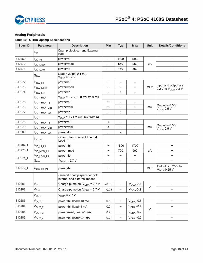
Two Opamps (Continuous-Time Block; CTB)
The PSoC 4100S has two opamps with Comparator modeswhich allow most common analog functions to be performedon-chip eliminating external components; PGAs, VoltageBuffers, Filters, Trans-Impedance Amplifiers, and other functionscan be realized, in some cases with external passives. savingpower, cost, and space. The on-chip opamps are designed withenough bandwidth to drive the Sample-and-Hold circuit of theADC without requiring external buffering.
Low-power Comparators (LPC)
The PSoC 4100S has a pair of low-power comparators, whichcan also operate in Deep Sleep modes. This allows the analogsystem blocks to be disabled while retaining the ability to monitorexternal voltage levels during low-power modes. Thecomparator outputs are normally synchronized to avoidmetastability unless operating in an asynchronous power modewhere the system wake-up circuit is activated by a comparatorswitch event. The LPC outputs can be routed to pins.
Current DACs
The PSoC 4100S has two IDACs, which can drive any of the pinson the chip. These IDACs have programmable current ranges.
Analog Multiplexed Buses
The PSoC 4100S has two concentric independent buses that goaround the periphery of the chip. These buses (called amuxbuses) are connected to firmware-programmable analogswitches that allow the chip's internal resources (IDACs,comparator) to connect to any pin on the I/O Ports.
Programmable Digital Blocks
The Programmable I/O (Smart I/O) block is a fabric of switchesand LUTs that allows Boolean functions to be performed insignals being routed to the pins of a GPIO port. The Smart I/Ocan perform logical operations on input pins to the chip and onsignals going out as outputs.
Fixed Function Digital
Timer/Counter/PWM (TCPWM) Block
The TCPWM block consists of a 16-bit counter withuser-programmable period length. There is a capture register torecord the count value at the time of an event (which may be anI/O event), a period register that is used to either stop orauto-reload the counter when its count is equal to the periodregister, and compare registers to generate compare valuesignals that are used as PWM duty cycle outputs. The block alsoprovides true and complementary outputs with programmableoffset between them to allow use as dead-band programmablecomplementary PWM outputs. It also has a Kill input to forceoutputs to a predetermined state; for example, this is used inmotor drive systems when an over-current state is indicated andthe PWM driving the FETs needs to be shut off immediately withno time for software intervention. There are five TCPWM blocksin the PSoC 4100S.
Serial Communication Block (SCB)
The PSoC 4100S has three serial communication blocks, which can be programmed to have SPI, I2C, or UART functionality.
SA
RM
UX
SA
RM
UX
Por
t
(U
p to
16
inp
uts)
vplu
svm
inus
Data and Status Flags
Reference Selection
External Reference and
Bypass (optional)
POS
NEG
SAR Sequencer
SARADC
Inputs from other Ports
VDDA/2 VDDA VREF
AHB System Bus and Programmable Logic Interconnect
Sequencing and Control
Document Number: 002-00122 Rev. *K Page 8 of 41
PSoC® 4: PSoC 4100S Datasheet
I2C Mode: The hardware I2C block implements a fullmulti-master and slave interface (it is capable of multi-masterarbitration). This block is capable of operating at speeds of up to400 kbps (Fast Mode) and has flexible buffering options toreduce interrupt overhead and latency for the CPU. It alsosupports EZI2C that creates a mailbox address range in thememory of the PSoC 4100S and effectively reduces I2C commu-nication to reading from and writing to an array in memory. Inaddition, the block supports an 8-deep FIFO for receive andtransmit which, by increasing the time given for the CPU to readdata, greatly reduces the need for clock stretching caused by theCPU not having read data on time.
The I2C peripheral is compatible with the I2C Standard-mode andFast-mode devices as defined in the NXP I2C-bus specificationand user manual (UM10204). The I2C bus I/O is implementedwith GPIO in open-drain modes.
The PSoC 4100S is not completely compliant with the I2C specin the following respect:
GPIO cells are not overvoltage tolerant and, therefore, cannotbe hot-swapped or powered up independently of the rest of theI2C system.
UART Mode: This is a full-feature UART operating at up to1 Mbps. It supports automotive single-wire interface (LIN),infrared interface (IrDA), and SmartCard (ISO7816) protocols, allof which are minor variants of the basic UART protocol. Inaddition, it supports the 9-bit multiprocessor mode that allowsaddressing of peripherals connected over common RX and TXlines. Common UART functions such as parity error, breakdetect, and frame error are supported. An 8-deep FIFO allowsmuch greater CPU service latencies to be tolerated.
SPI Mode: The SPI mode supports full Motorola SPI, TI SSP(adds a start pulse used to synchronize SPI Codecs), andNational Microwire (half-duplex form of SPI). The SPI block canuse the FIFO.
GPIO
The PSoC 4100S has up to 36 GPIOs. The GPIO block imple-ments the following:
Eight drive modes: Analog input mode (input and output buffers disabled) Input only Weak pull-up with strong pull-down Strong pull-up with weak pull-down Open drain with strong pull-down Open drain with strong pull-up Strong pull-up with strong pull-down Weak pull-up with weak pull-down
Input threshold select (CMOS or LVTTL).
Individual control of input and output buffer enabling/disablingin addition to the drive strength modes
Selectable slew rates for dV/dt related noise control to improveEMI
The pins are organized in logical entities called ports, which are8-bit in width (less for Ports 2 and 3). During power-on and reset,the blocks are forced to the disable state so as not to crowbarany inputs and/or cause excess turn-on current. A multiplexingnetwork known as a high-speed I/O matrix is used to multiplexbetween various signals that may connect to an I/O pin.
Data output and pin state registers store, respectively, the valuesto be driven on the pins and the states of the pins themselves.
Every I/O pin can generate an interrupt if so enabled and eachI/O port has an interrupt request (IRQ) and interrupt serviceroutine (ISR) vector associated with it (5 for PSoC 4100S).
Special Function Peripherals
CapSense
CapSense is supported in the PSoC 4100S through a CapSenseSigma-Delta (CSD) block that can be connected to any pinsthrough an analog multiplex bus via analog switches. CapSensefunction can thus be provided on any available pin or group ofpins in a system under software control. A PSoC Creatorcomponent is provided for the CapSense block to make it easyfor the user.
Shield voltage can be driven on another analog multiplex bus toprovide water-tolerance capability. Water tolerance is providedby driving the shield electrode in phase with the sense electrodeto keep the shield capacitance from attenuating the sensedinput. Proximity sensing can also be implemented.
The CapSense block has two IDACs, which can be used forgeneral purposes if CapSense is not being used (both IDACs areavailable in that case) or if CapSense is used without watertolerance (one IDAC is available).
The CapSense block also provides a 10-bit Slope ADC functionwhich can be used in conjunction with the CapSense function.
The CapSense block is an advanced, low-noise, programmableblock with programmable voltage references and current sourceranges for improved sensitivity and flexibility. It can also use anexternal reference voltage. It has a full-wave CSD mode thatalternates sensing to VDDA and ground to null out power-supplyrelated noise.
LCD Segment Drive
The PSoC 4100S has an LCD controller, which can drive up to4 commons and up to 32 segments. It uses full digital methodsto drive the LCD segments requiring no generation of internalLCD voltages. The two methods used are referred to as DigitalCorrelation and PWM. Digital Correlation pertains to modulatingthe frequency and drive levels of the common and segmentsignals to generate the highest RMS voltage across a segmentto light it up or to keep the RMS signal to zero. This method isgood for STN displays but may result in reduced contrast with TN(cheaper) displays. PWM pertains to driving the panel with PWMsignals to effectively use the capacitance of the panel to providethe integration of the modulated pulse-width to generate thedesired LCD voltage. This method results in higher powerconsumption but can result in better results when driving TNdisplays. LCD operation is supported during Deep Sleeprefreshing a small display buffer (4 bits; 1 32-bit register per port).
Document Number: 002-00122 Rev. *K Page 9 of 41
PSoC® 4: PSoC 4100S Datasheet
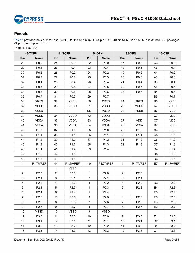
Pinouts
Table 1 provides the pin list for PSoC 4100S for the 48-pin TQFP, 44-pin TQFP, 40-pin QFN, 32-pin QFN, and 35-ball CSP packages. All port pins support GPIO.
Table 1. Pin List
48-TQFP 44-TQFP 40-QFN 32-QFN 35-CSP
Pin Name Pin Name Pin Name Pin Name Pin Name
28 P0.0 24 P0.0 22 P0.0 17 P0.0 C3 P0.0
29 P0.1 25 P0.1 23 P0.1 18 P0.1 A5 P0.1
30 P0.2 26 P0.2 24 P0.2 19 P0.2 A4 P0.2
31 P0.3 27 P0.3 25 P0.3 20 P0.3 A3 P0.3
32 P0.4 28 P0.4 26 P0.4 21 P0.4 B3 P0.4
33 P0.5 29 P0.5 27 P0.5 22 P0.5 A6 P0.5
34 P0.6 30 P0.6 28 P0.6 23 P0.6 B4 P0.6
35 P0.7 31 P0.7 29 P0.7 B5 P0.7
36 XRES 32 XRES 30 XRES 24 XRES B6 XRES
37 VCCD 33 VCCD 31 VCCD 25 VCCD A7 VCCD
38 VSSD DN VSSD 26 VSSD B7 VSS
39 VDDD 34 VDDD 32 VDDD C7 VDD
40 VDDA 35 VDDA 33 VDDA 27 VDD C7 VDD
41 VSSA 36 VSSA 34 VSSA 28 VSSA B7 VSS
42 P1.0 37 P1.0 35 P1.0 29 P1.0 C4 P1.0
43 P1.1 38 P1.1 36 P1.1 30 P1.1 C5 P1.1
44 P1.2 39 P1.2 37 P1.2 31 P1.2 C6 P1.2
45 P1.3 40 P1.3 38 P1.3 32 P1.3 D7 P1.3
46 P1.4 41 P1.4 39 P1.4 D4 P1.4
47 P1.5 42 P1.5 D5 P1.5
48 P1.6 43 P1.6 D6 P1.6
1 P1.7/VREF 44 P1.7/VREF 40 P1.7/VREF 1 P1.7/VREF E7 P1.7/VREF
1 VSSD
2 P2.0 2 P2.0 1 P2.0 2 P2.0
3 P2.1 3 P2.1 2 P2.1 3 P2.1
4 P2.2 4 P2.2 3 P2.2 4 P2.2 D3 P2.2
5 P2.3 5 P2.3 4 P2.3 5 P2.3 E4 P2.3
6 P2.4 6 P2.4 5 P2.4 E5 P2.4
7 P2.5 7 P2.5 6 P2.5 6 P2.5 E6 P2.5
8 P2.6 8 P2.6 7 P2.6 7 P2.6 E3 P2.6
9 P2.7 9 P2.7 8 P2.7 8 P2.7 E2 P2.7
10 VSSD 10 VSSD 9 VSSD
12 P3.0 11 P3.0 10 P3.0 9 P3.0 E1 P3.0
13 P3.1 12 P3.1 11 P3.1 10 P3.1 D2 P3.1
14 P3.2 13 P3.2 12 P3.2 11 P3.2 D1 P3.2
16 P3.3 14 P3.3 13 P3.3 12 P3.3 C1 P3.3
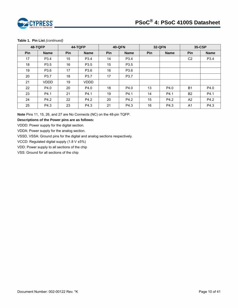
Document Number: 002-00122 Rev. *K Page 10 of 41
PSoC® 4: PSoC 4100S Datasheet
Note Pins 11, 15, 26, and 27 are No Connects (NC) on the 48-pin TQFP.
Descriptions of the Power pins are as follows:
VDDD: Power supply for the digital section.
VDDA: Power supply for the analog section.
VSSD, VSSA: Ground pins for the digital and analog sections respectively.
VCCD: Regulated digital supply (1.8 V ±5%)
VDD: Power supply to all sections of the chip
VSS: Ground for all sections of the chip
17 P3.4 15 P3.4 14 P3.4 C2 P3.4
18 P3.5 16 P3.5 15 P3.5
19 P3.6 17 P3.6 16 P3.6
20 P3.7 18 P3.7 17 P3.7
21 VDDD 19 VDDD
22 P4.0 20 P4.0 18 P4.0 13 P4.0 B1 P4.0
23 P4.1 21 P4.1 19 P4.1 14 P4.1 B2 P4.1
24 P4.2 22 P4.2 20 P4.2 15 P4.2 A2 P4.2
25 P4.3 23 P4.3 21 P4.3 16 P4.3 A1 P4.3
Table 1. Pin List (continued)
48-TQFP 44-TQFP 40-QFN 32-QFN 35-CSP
Pin Name Pin Name Pin Name Pin Name Pin Name
Document Number: 002-00122 Rev. *K Page 11 of 41
PSoC® 4: PSoC 4100S Datasheet
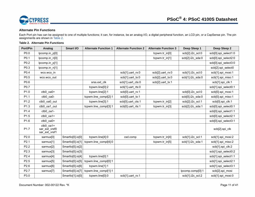
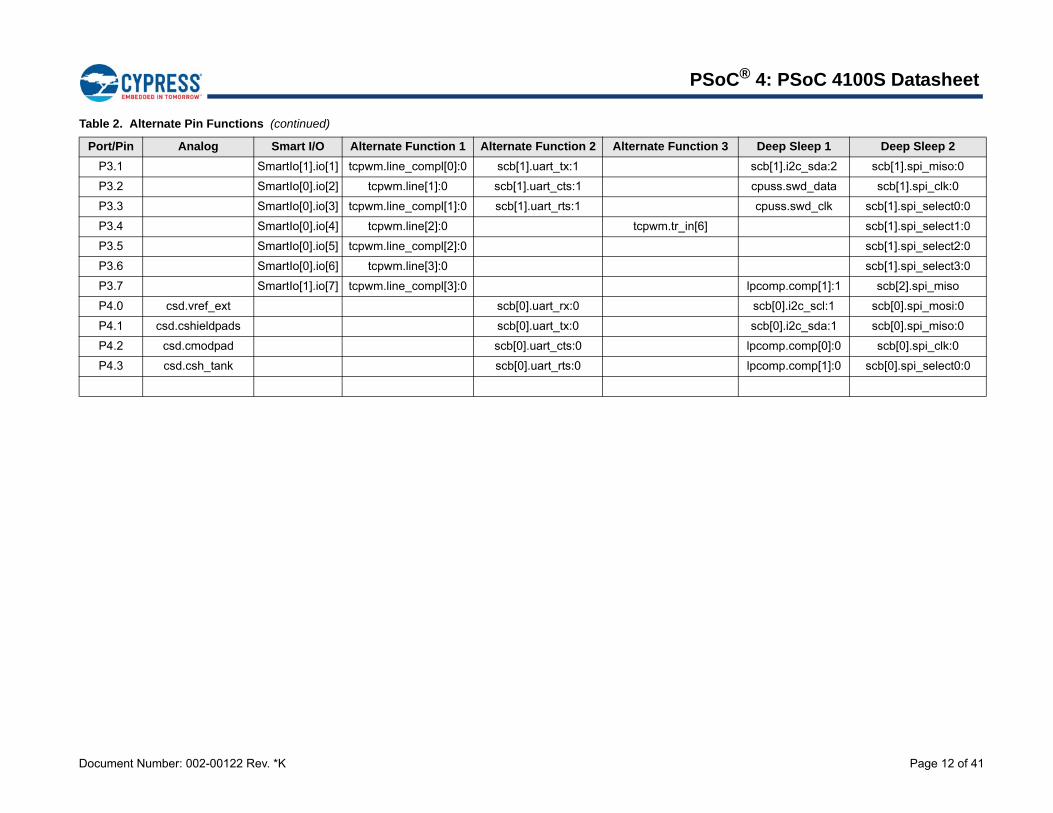
Alternate Pin Functions
Each Port pin has can be assigned to one of multiple functions; it can, for instance, be an analog I/O, a digital peripheral function, an LCD pin, or a CapSense pin. The pin assignments are shown in Table 2.
Table 2. Alternate Pin Functions
Port/Pin Analog Smart I/O Alternate Function 1 Alternate Function 2 Alternate Function 3 Deep Sleep 1 Deep Sleep 2
P0.0 lpcomp.in_p[0] tcpwm.tr_in[0] scb[2].i2c_scl:0 scb[0].spi_select1:0
P0.1 lpcomp.in_n[0] tcpwm.tr_in[1] scb[2].i2c_sda:0 scb[0].spi_select2:0
P0.2 lpcomp.in_p[1] scb[0].spi_select3:0
P0.3 lpcomp.in_n[1] scb[2].spi_select0
P0.4 wco.wco_in scb[1].uart_rx:0 scb[2].uart_rx:0 scb[1].i2c_scl:0 scb[1].spi_mosi:1
P0.5 wco.wco_out scb[1].uart_tx:0 scb[2].uart_tx:0 scb[1].i2c_sda:0 scb[1].spi_miso:1
P0.6 srss.ext_clk scb[1].uart_cts:0 scb[2].uart_tx:1 scb[1].spi_clk:1
P0.7 tcpwm.line[0]:2 scb[1].uart_rts:0 scb[1].spi_select0:1
P1.0 ctb0_oa0+ tcpwm.line[2]:1 scb[0].uart_rx:1 scb[0].i2c_scl:0 scb[0].spi_mosi:1
P1.1 ctb0_oa0- tcpwm.line_compl[2]:1 scb[0].uart_tx:1 scb[0].i2c_sda:0 scb[0].spi_miso:1
P1.2 ctb0_oa0_out tcpwm.line[3]:1 scb[0].uart_cts:1 tcpwm.tr_in[2] scb[2].i2c_scl:1 scb[0].spi_clk:1
P1.3 ctb0_oa1_out tcpwm.line_compl[3]:1 scb[0].uart_rts:1 tcpwm.tr_in[3] scb[2].i2c_sda:1 scb[0].spi_select0:1
P1.4 ctb0_oa1- scb[0].spi_select1:1
P1.5 ctb0_oa1+ scb[0].spi_select2:1
P1.6 ctb0_oa0+ scb[0].spi_select3:1
P1.7ctb0_oa1+
sar_ext_vref0sar_ext_vref1
scb[2].spi_clk
P2.0 sarmux[0] SmartIo[0].io[0] tcpwm.line[4]:0 csd.comp tcpwm.tr_in[4] scb[1].i2c_scl:1 scb[1].spi_mosi:2
P2.1 sarmux[1] SmartIo[0].io[1] tcpwm.line_compl[4]:0 tcpwm.tr_in[5] scb[1].i2c_sda:1 scb[1].spi_miso:2
P2.2 sarmux[2] SmartIo[0].io[2] scb[1].spi_clk:2
P2.3 sarmux[3] SmartIo[0].io[3] scb[1].spi_select0:2
P2.4 sarmux[4] SmartIo[0].io[4] tcpwm.line[0]:1 scb[1].spi_select1:1
P2.5 sarmux[5] SmartIo[0].io[5] tcpwm.line_compl[0]:1 scb[1].spi_select2:1
P2.6 sarmux[6] SmartIo[0].io[6] tcpwm.line[1]:1 scb[1].spi_select3:1
P2.7 sarmux[7] SmartIo[0].io[7] tcpwm.line_compl[1]:1 lpcomp.comp[0]:1 scb[2].spi_mosi
P3.0 SmartIo[1].io[0] tcpwm.line[0]:0 scb[1].uart_rx:1 scb[1].i2c_scl:2 scb[1].spi_mosi:0
Document Number: 002-00122 Rev. *K Page 12 of 41
PSoC® 4: PSoC 4100S Datasheet
P3.1 SmartIo[1].io[1] tcpwm.line_compl[0]:0 scb[1].uart_tx:1 scb[1].i2c_sda:2 scb[1].spi_miso:0
P3.2 SmartIo[0].io[2] tcpwm.line[1]:0 scb[1].uart_cts:1 cpuss.swd_data scb[1].spi_clk:0
P3.3 SmartIo[0].io[3] tcpwm.line_compl[1]:0 scb[1].uart_rts:1 cpuss.swd_clk scb[1].spi_select0:0
P3.4 SmartIo[0].io[4] tcpwm.line[2]:0 tcpwm.tr_in[6] scb[1].spi_select1:0
P3.5 SmartIo[0].io[5] tcpwm.line_compl[2]:0 scb[1].spi_select2:0
P3.6 SmartIo[0].io[6] tcpwm.line[3]:0 scb[1].spi_select3:0
P3.7 SmartIo[1].io[7] tcpwm.line_compl[3]:0 lpcomp.comp[1]:1 scb[2].spi_miso
P4.0 csd.vref_ext scb[0].uart_rx:0 scb[0].i2c_scl:1 scb[0].spi_mosi:0
P4.1 csd.cshieldpads scb[0].uart_tx:0 scb[0].i2c_sda:1 scb[0].spi_miso:0
P4.2 csd.cmodpad scb[0].uart_cts:0 lpcomp.comp[0]:0 scb[0].spi_clk:0
P4.3 csd.csh_tank scb[0].uart_rts:0 lpcomp.comp[1]:0 scb[0].spi_select0:0
Table 2. Alternate Pin Functions (continued)
Port/Pin Analog Smart I/O Alternate Function 1 Alternate Function 2 Alternate Function 3 Deep Sleep 1 Deep Sleep 2
Document Number: 002-00122 Rev. *K Page 13 of 41
PSoC® 4: PSoC 4100S Datasheet
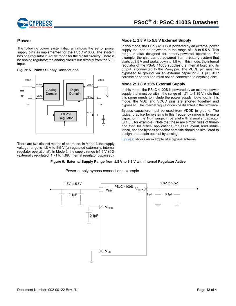
Power
The following power system diagram shows the set of powersupply pins as implemented for the PSoC 4100S. The systemhas one regulator in Active mode for the digital circuitry. There isno analog regulator; the analog circuits run directly from the VDDinput.
Figure 5. Power Supply Connections
There are two distinct modes of operation. In Mode 1, the supplyvoltage range is 1.8 V to 5.5 V (unregulated externally; internalregulator operational). In Mode 2, the supply range is1.8 V ±5%(externally regulated; 1.71 to 1.89, internal regulator bypassed).
Mode 1: 1.8 V to 5.5 V External Supply
In this mode, the PSoC 4100S is powered by an external powersupply that can be anywhere in the range of 1.8 to 5.5 V. Thisrange is also designed for battery-powered operation. Forexample, the chip can be powered from a battery system thatstarts at 3.5 V and works down to 1.8 V. In this mode, the internalregulator of the PSoC 4100S supplies the internal logic and itsoutput is connected to the VCCD pin. The VCCD pin must bebypassed to ground via an external capacitor (0.1 µF; X5Rceramic or better) and must not be connected to anything else.
Mode 2: 1.8 V ±5% External Supply
In this mode, the PSoC 4100S is powered by an external powersupply that must be within the range of 1.71 to 1.89 V; note thatthis range needs to include the power supply ripple too. In thismode, the VDD and VCCD pins are shorted together andbypassed. The internal regulator can be disabled in the firmware.
Bypass capacitors must be used from VDDD to ground. Thetypical practice for systems in this frequency range is to use acapacitor in the 1-µF range, in parallel with a smaller capacitor(0.1 µF, for example). Note that these are simply rules of thumband that, for critical applications, the PCB layout, lead induc-tance, and the bypass capacitor parasitic should be simulated todesign and obtain optimal bypassing.
Figure 6 shows an example of a bypass scheme.
Figure 6. External Supply Range from 1.8 V to 5.5 V with Internal Regulator Active
AnalogDomain
VDDA
VSSA
VDDA
1.8 VoltRegulator
DigitalDomain
VDDD
VSSD
VDDD
VCCD
PSoC 4100SVDD
VSS
1.8V to 5.5V
0.1F
VCCD
0.1F
Power supply bypass connections example
1.8V to 5.5V
0.1FF
VDDA
Document Number: 002-00122 Rev. *K Page 14 of 41
PSoC® 4: PSoC 4100S Datasheet
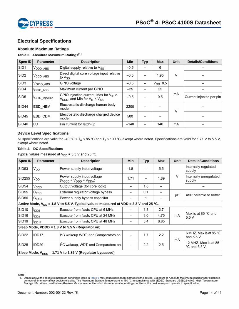
Electrical Specifications
Absolute Maximum Ratings
Device Level Specifications
All specifications are valid for –40 °C TA 85 °C and TJ 100 °C, except where noted. Specifications are valid for 1.71 V to 5.5 V, except where noted.
Note1. Usage above the absolute maximum conditions listed in Table 3 may cause permanent damage to the device. Exposure to Absolute Maximum conditions for extended
periods of time may affect device reliability. The Maximum Storage Temperature is 150 °C in compliance with JEDEC Standard JESD22-A103, High Temperature Storage Life. When used below Absolute Maximum conditions but above normal operating conditions, the device may not operate to specification.
Table 3. Absolute Maximum Ratings[1]
Spec ID Parameter Description Min Typ Max Unit Details/Conditions
SID1 VDDD_ABS Digital supply relative to VSS –0.5 – 6
V
–
SID2 VCCD_ABSDirect digital core voltage input relative to VSS
–0.5 – 1.95 –
SID3 VGPIO_ABS GPIO voltage –0.5 – VDD+0.5 –
SID4 IGPIO_ABS Maximum current per GPIO –25 – 25mA
–
SID5 IGPIO_injection GPIO injection current, Max for VIH > VDDD, and Min for VIL < VSS
–0.5 – 0.5 Current injected per pin
BID44 ESD_HBMElectrostatic discharge human body model 2200 – –
V–
BID45 ESD_CDM Electrostatic discharge charged device model
500 – – –
BID46 LU Pin current for latch-up –140 – 140 mA –
Table 4. DC Specifications
Typical values measured at VDD = 3.3 V and 25 °C.
Spec ID Parameter Description Min Typ Max Unit Details/Conditions
SID53 VDD Power supply input voltage 1.8 – 5.5
V
Internally regulated supply
SID255 VDDPower supply input voltage (VCCD = VDDD = VDDA)
1.71 – 1.89 Internally unregulated supply
SID54 VCCD Output voltage (for core logic) – 1.8 – –
SID55 CEFC External regulator voltage bypass – 0.1 –µF X5R ceramic or better
SID56 CEXC Power supply bypass capacitor – 1 –
Active Mode, VDD = 1.8 V to 5.5 V. Typical values measured at VDD = 3.3 V and 25 °C.
SID10 IDD5 Execute from flash; CPU at 6 MHz – 1.8 2.7
mAMax is at 85 °C and 5.5 VSID16 IDD8 Execute from flash; CPU at 24 MHz – 3.0 4.75
SID19 IDD11 Execute from flash; CPU at 48 MHz – 5.4 6.85
Sleep Mode, VDDD = 1.8 V to 5.5 V (Regulator on)
SID22 IDD17 I2C wakeup WDT, and Comparators on – 1.7 2.2mA
6 MHZ. Max is at 85 °C and 5.5 V.
SID25 IDD20 I2C wakeup, WDT, and Comparators on. – 2.2 2.512 MHZ. Max is at 85 °C and 5.5 V.
Sleep Mode, VDDD = 1.71 V to 1.89 V (Regulator bypassed)
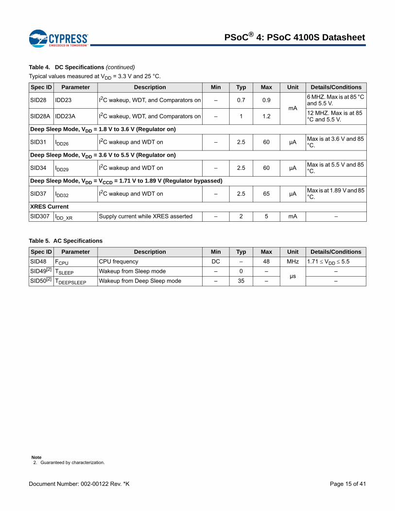
Document Number: 002-00122 Rev. *K Page 15 of 41
PSoC® 4: PSoC 4100S Datasheet
SID28 IDD23 I2C wakeup, WDT, and Comparators on – 0.7 0.9mA
6 MHZ. Max is at 85 °C and 5.5 V.
SID28A IDD23A I2C wakeup, WDT, and Comparators on – 1 1.212 MHZ. Max is at 85 °C and 5.5 V.
Deep Sleep Mode, VDD = 1.8 V to 3.6 V (Regulator on)
SID31 IDD26 I2C wakeup and WDT on – 2.5 60 µA Max is at 3.6 V and 85 °C.
Deep Sleep Mode, VDD = 3.6 V to 5.5 V (Regulator on)
SID34 IDD29 I2C wakeup and WDT on – 2.5 60 µA Max is at 5.5 V and 85 °C.
Deep Sleep Mode, VDD = VCCD = 1.71 V to 1.89 V (Regulator bypassed)
SID37 IDD32 I2C wakeup and WDT on – 2.5 65 µAMax is at 1.89 V and 85 °C.
XRES Current
SID307 IDD_XR Supply current while XRES asserted – 2 5 mA –
Table 4. DC Specifications (continued)
Typical values measured at VDD = 3.3 V and 25 °C.
Spec ID Parameter Description Min Typ Max Unit Details/Conditions
Note2. Guaranteed by characterization.
Table 5. AC Specifications
Spec ID Parameter Description Min Typ Max Unit Details/Conditions
SID48 FCPU CPU frequency DC – 48 MHz 1.71 VDD 5.5
SID49[2] TSLEEP Wakeup from Sleep mode – 0 –µs
–
SID50[2] TDEEPSLEEP Wakeup from Deep Sleep mode – 35 – –
Document Number: 002-00122 Rev. *K Page 16 of 41
PSoC® 4: PSoC 4100S Datasheet
GPIO
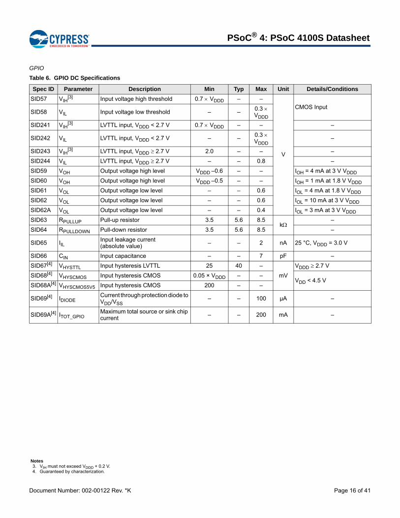
Table 6. GPIO DC Specifications
Spec ID Parameter Description Min Typ Max Unit Details/Conditions
SID57 VIH[3] Input voltage high threshold 0.7 VDDD – –
V
CMOS InputSID58 VIL Input voltage low threshold – –
0.3 VDDD
SID241 VIH[3] LVTTL input, VDDD < 2.7 V 0.7 VDDD – – –
SID242 VIL LVTTL input, VDDD < 2.7 V – – 0.3 VDDD
–
SID243 VIH[3] LVTTL input, VDDD 2.7 V 2.0 – – –
SID244 VIL LVTTL input, VDDD 2.7 V – – 0.8 –
SID59 VOH Output voltage high level VDDD –0.6 – – IOH = 4 mA at 3 V VDDD
SID60 VOH Output voltage high level VDDD –0.5 – – IOH = 1 mA at 1.8 V VDDD
SID61 VOL Output voltage low level – – 0.6 IOL = 4 mA at 1.8 V VDDD
SID62 VOL Output voltage low level – – 0.6 IOL = 10 mA at 3 V VDDD
SID62A VOL Output voltage low level – – 0.4 IOL = 3 mA at 3 V VDDD
SID63 RPULLUP Pull-up resistor 3.5 5.6 8.5k
–
SID64 RPULLDOWN Pull-down resistor 3.5 5.6 8.5 –
SID65 IILInput leakage current (absolute value) – – 2 nA 25 °C, VDDD = 3.0 V
SID66 CIN Input capacitance – – 7 pF –
SID67[4] VHYSTTL Input hysteresis LVTTL 25 40 –
mV
VDDD 2.7 V
SID68[4] VHYSCMOS Input hysteresis CMOS 0.05 × VDDD – –VDD < 4.5 V
SID68A[4] VHYSCMOS5V5 Input hysteresis CMOS 200 – –
SID69[4] IDIODECurrent through protection diode to VDD/VSS
– – 100 µA –
SID69A[4] ITOT_GPIOMaximum total source or sink chip current
– – 200 mA –
Notes3. VIH must not exceed VDDD + 0.2 V.4. Guaranteed by characterization.
Document Number: 002-00122 Rev. *K Page 17 of 41
PSoC® 4: PSoC 4100S Datasheet
XRES
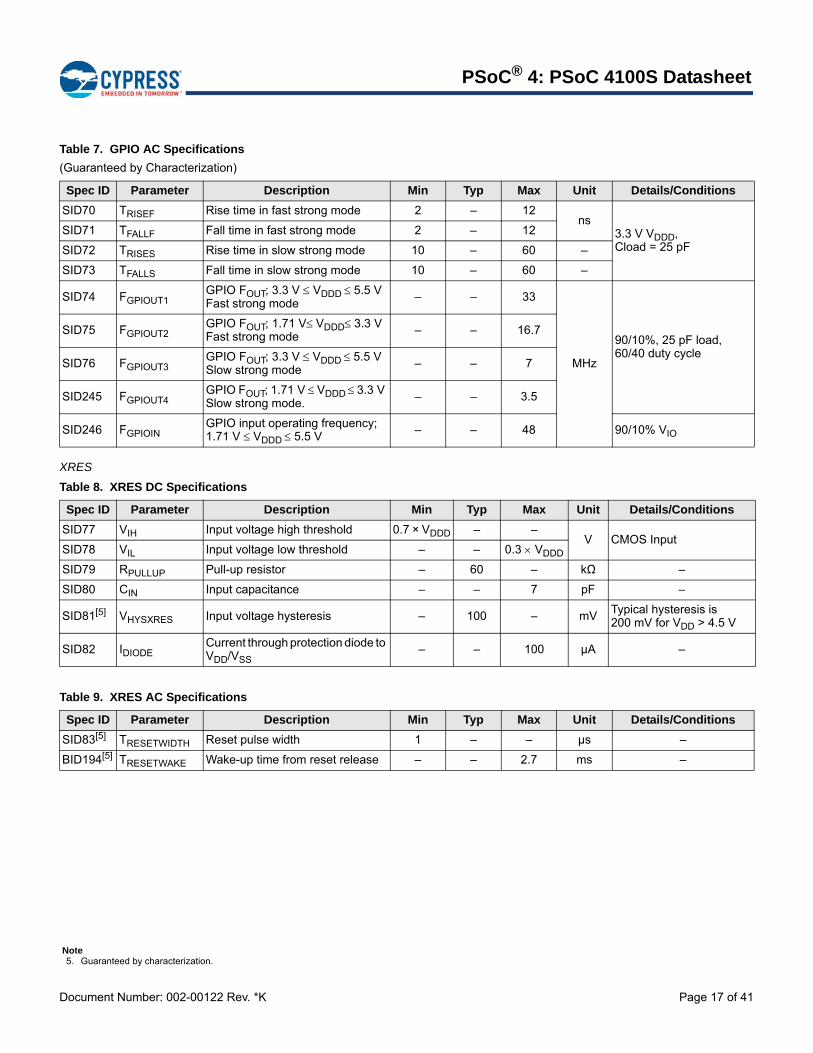
Table 7. GPIO AC Specifications
(Guaranteed by Characterization)
Spec ID Parameter Description Min Typ Max Unit Details/Conditions
SID70 TRISEF Rise time in fast strong mode 2 – 12ns
3.3 V VDDD, Cload = 25 pF
SID71 TFALLF Fall time in fast strong mode 2 – 12
SID72 TRISES Rise time in slow strong mode 10 – 60 –
SID73 TFALLS Fall time in slow strong mode 10 – 60 –
SID74 FGPIOUT1GPIO FOUT; 3.3 V VDDD 5.5 V Fast strong mode
– – 33
MHz
90/10%, 25 pF load, 60/40 duty cycle
SID75 FGPIOUT2GPIO FOUT; 1.71 VVDDD3.3 V Fast strong mode – – 16.7
SID76 FGPIOUT3GPIO FOUT; 3.3 V VDDD 5.5 V Slow strong mode – – 7
SID245 FGPIOUT4GPIO FOUT; 1.71 V VDDD 3.3 V Slow strong mode.
– – 3.5
SID246 FGPIOINGPIO input operating frequency;1.71 V VDDD 5.5 V – – 48 90/10% VIO
Note5. Guaranteed by characterization.
Table 8. XRES DC Specifications
Spec ID Parameter Description Min Typ Max Unit Details/Conditions
SID77 VIH Input voltage high threshold 0.7 × VDDD – –V CMOS Input
SID78 VIL Input voltage low threshold – – 0.3 VDDD
SID79 RPULLUP Pull-up resistor – 60 – kΩ –
SID80 CIN Input capacitance – – 7 pF –
SID81[5] VHYSXRES Input voltage hysteresis – 100 – mV Typical hysteresis is 200 mV for VDD > 4.5 V
SID82 IDIODECurrent through protection diode to VDD/VSS
– – 100 µA –
Table 9. XRES AC Specifications
Spec ID Parameter Description Min Typ Max Unit Details/Conditions
SID83[5] TRESETWIDTH Reset pulse width 1 – – µs –
BID194[5] TRESETWAKE Wake-up time from reset release – – 2.7 ms –
Document Number: 002-00122 Rev. *K Page 18 of 41
PSoC® 4: PSoC 4100S Datasheet
Analog Peripherals
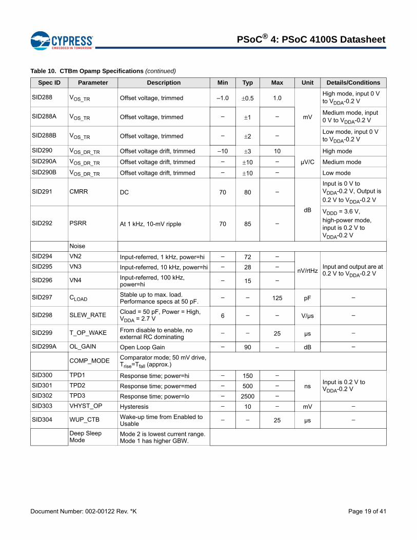
Table 10. CTBm Opamp Specifications
Spec ID Parameter Description Min Typ Max Unit Details/Conditions
IDDOpamp block current, External load
SID269 IDD_HI power=hi – 1100 1850
µA
–
SID270 IDD_MED power=med – 550 950 –
SID271 IDD_LOW power=lo – 150 350 –
GBWLoad = 20 pF, 0.1 mAVDDA = 2.7 V
SID272 GBW_HI power=hi 6 – –
MHz Input and output are 0.2 V to VDDA-0.2 V
SID273 GBW_MED power=med 3 – –
SID274 GBW_LO power=lo – 1 –
IOUT_MAX VDDA = 2.7 V, 500 mV from rail
SID275 IOUT_MAX_HI power=hi 10 – –
mA Output is 0.5 V VDDA-0.5 V
SID276 IOUT_MAX_MID power=mid 10 – –
SID277 IOUT_MAX_LO power=lo – 5 –
IOUT VDDA = 1.71 V, 500 mV from rail
SID278 IOUT_MAX_HI power=hi 4 – –
mA Output is 0.5 V VDDA-0.5 VSID279 IOUT_MAX_MID power=mid 4 – –
SID280 IOUT_MAX_LO power=lo – 2 –
IDD_IntOpamp block current Internal Load
SID269_I IDD_HI_Int power=hi – 1500 1700
µA
–
SID270_I IDD_MED_Int power=med – 700 900 –
SID271_IIDD_LOW_Int power=lo – – – –
GBW VDDA = 2.7 V – – – –
SID272_I GBW_HI_Int power=hi 8 – – MHzOutput is 0.25 V to VDDA-0.25 V
General opamp specs for both internal and external modes
SID281 VIN Charge-pump on, VDDA = 2.7 V –0.05 – VDDA-0.2V
–
SID282 VCM Charge-pump on, VDDA = 2.7 V –0.05 – VDDA-0.2 –
VOUT VDDA = 2.7 V
SID283 VOUT_1 power=hi, Iload=10 mA 0.5 – VDDA -0.5
V
–
SID284 VOUT_2 power=hi, Iload=1 mA 0.2 – VDDA -0.2 –
SID285 VOUT_3 power=med, Iload=1 mA 0.2 – VDDA -0.2 –
SID286 VOUT_4 power=lo, Iload=0.1 mA 0.2 – VDDA -0.2 –
Document Number: 002-00122 Rev. *K Page 19 of 41
PSoC® 4: PSoC 4100S Datasheet
SID288 VOS_TR Offset voltage, trimmed –1.0 0.5 1.0
mV
High mode, input 0 V to VDDA-0.2 V
SID288A VOS_TR Offset voltage, trimmed – 1 –Medium mode, input 0 V to VDDA-0.2 V
SID288B VOS_TR Offset voltage, trimmed – 2 –Low mode, input 0 V to VDDA-0.2 V
SID290 VOS_DR_TR Offset voltage drift, trimmed –10 3 10
µV/C
High mode
SID290A VOS_DR_TR Offset voltage drift, trimmed – 10 – Medium mode
SID290B VOS_DR_TR Offset voltage drift, trimmed – 10 – Low mode
SID291 CMRR DC 70 80 –
dB
Input is 0 V to VDDA-0.2 V, Output is
0.2 V to VDDA-0.2 V
SID292 PSRR At 1 kHz, 10-mV ripple 70 85 –
VDDD = 3.6 V,
high-power mode, input is 0.2 V to VDDA-0.2 V
Noise
SID294 VN2 Input-referred, 1 kHz, power=hi – 72 –
nV/rtHzInput and output are at 0.2 V to VDDA-0.2 V
SID295 VN3 Input-referred, 10 kHz, power=hi – 28 –
SID296 VN4 Input-referred, 100 kHz, power=hi
– 15 –
SID297 CLOADStable up to max. load. Performance specs at 50 pF.
– – 125 pF –
SID298 SLEW_RATE Cload = 50 pF, Power = High, VDDA = 2.7 V 6 – – V/µs –
SID299 T_OP_WAKE From disable to enable, no external RC dominating
– – 25 µs –
SID299A OL_GAIN Open Loop Gain – 90 – dB –
COMP_MODE Comparator mode; 50 mV drive, Trise=Tfall (approx.)
SID300 TPD1 Response time; power=hi – 150 –
nsInput is 0.2 V to VDDA-0.2 V
SID301 TPD2 Response time; power=med – 500 –
SID302 TPD3 Response time; power=lo – 2500 –
SID303 VHYST_OP Hysteresis – 10 – mV –
SID304 WUP_CTB Wake-up time from Enabled to Usable
– – 25 µs –
Deep Sleep Mode
Mode 2 is lowest current range. Mode 1 has higher GBW.
Table 10. CTBm Opamp Specifications (continued)
Spec ID Parameter Description Min Typ Max Unit Details/Conditions
Document Number: 002-00122 Rev. *K Page 20 of 41
PSoC® 4: PSoC 4100S Datasheet
SID_DS_1 IDD_HI_M1 Mode 1, High current – 1400 –
µA 25 °C
SID_DS_2 IDD_MED_M1 Mode 1, Medium current – 700 –
SID_DS_3 IDD_LOW_M1 Mode 1, Low current – 200 –
SID_DS_4 IDD_HI_M2 Mode 2, High current – 120 –
SID_DS_5 IDD_MED_M2 Mode 2, Medium current – 60 –
SID_DS_6 IDD_LOW_M2 Mode 2, Low current – 15 –
SID_DS_7 GBW_HI_M1 Mode 1, High current – 4 –
MHz20-pF load, no DC load 0.2 V to VDDA-0.2 V
SID_DS_8 GBW_MED_M1 Mode 1, Medium current – 2 –
SID_DS_9 GBW_LOW_M! Mode 1, Low current – 0.5 –
SID_DS_10 GBW_HI_M2 Mode 2, High current – 0.5 –
SID_DS_11 GBW_MED_M2 Mode 2, Medium current – 0.2 –
SID_DS_12 GBW_Low_M2 Mode 2, Low current – 0.1 –
SID_DS_13 VOS_HI_M1 Mode 1, High current – 5 –
mVWith trim 25 °C, 0.2 V to VDDA-0.2 V
SID_DS_14 VOS_MED_M1 Mode 1, Medium current – 5 –
SID_DS_15 VOS_LOW_M2 Mode 1, Low current – 5 –
SID_DS_16 VOS_HI_M2 Mode 2, High current – 5 –
SID_DS_17 VOS_MED_M2 Mode 2, Medium current – 5 –
SID_DS_18 VOS_LOW_M2 Mode 2, Low current – 5 –
SID_DS_19 IOUT_HI_M! Mode 1, High current – 10 –
mA
Output is 0.5 V to VDDA-0.5 V
SID_DS_20 IOUT_MED_M1 Mode 1, Medium current – 10 –
SID_DS_21 IOUT_LOW_M1 Mode 1, Low current – 4 –
SID_DS_22 IOUT_HI_M2 Mode 2, High current – 1 – –
SID_DS_23 IOU_MED_M2 Mode 2, Medium current – 1 – –
SID_DS_24 IOU_LOW_M2 Mode 2, Low current – 0.5 – –
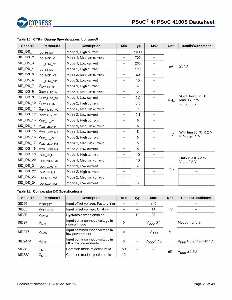
Table 11. Comparator DC Specifications
Spec ID Parameter Description Min Typ Max Unit Details/Conditions
SID84 VOFFSET1 Input offset voltage, Factory trim – – ±10
mV
–
SID85 VOFFSET2 Input offset voltage, Custom trim – – ±4 –
SID86 VHYST Hysteresis when enabled – 10 35 –
SID87 VICM1Input common mode voltage in normal mode 0 – VDDD-0.1
V
Modes 1 and 2
SID247 VICM2Input common mode voltage in low power mode 0 – VDDD –
SID247A VICM3Input common mode voltage in ultra low power mode
0 – VDDD-1.15 VDDD ≥ 2.2 V at –40 °C
SID88 CMRR Common mode rejection ratio 50 – –dB VDDD ≥ 2.7V
SID88A CMRR Common mode rejection ratio 42 – –
Table 10. CTBm Opamp Specifications (continued)
Spec ID Parameter Description Min Typ Max Unit Details/Conditions
Document Number: 002-00122 Rev. *K Page 21 of 41
PSoC® 4: PSoC 4100S Datasheet
SID89 ICMP1 Block current, normal mode – – 400
µA
–
SID248 ICMP2 Block current, low power mode – – 100 –
SID259 ICMP3Block current in ultra low-power mode – – 6
VDDD ≥ 2.2 V at –40 °C
SID90 ZCMPDC Input impedance of comparator
35 – – MΩ –
Table 11. Comparator DC Specifications (continued)
Spec ID Parameter Description Min Typ Max Unit Details/Conditions
Table 12. Comparator AC Specifications
Spec ID Parameter Description Min Typ Max Unit Details/Conditions
SID91 TRESP1Response time, normal mode, 50 mV overdrive – 38 110
ns–
SID258 TRESP2 Response time, low power mode, 50 mV overdrive
– 70 200 –
SID92 TRESP3 Response time, ultra-low power mode, 200 mV overdrive – 2.3 15 µs VDDD ≥ 2.2 V at –40 °C
Table 13. Temperature Sensor Specifications
Spec ID Parameter Description Min Typ Max Unit Details/Conditions
SID93 TSENSACC Temperature sensor accuracy –5 ±1 5 °C –40 to +85 °C
Table 14. SAR Specifications
Spec ID Parameter Description Min Typ Max Unit Details/Conditions
SAR ADC DC Specifications
SID94 A_RES Resolution – – 12 bits –
SID95 A_CHNLS_S Number of channels - single ended – – 16 –
SID96 A-CHNKS_D Number of channels - differential – – 4Diff inputs use neighboring I/O
SID97 A-MONO Monotonicity – – – Yes
SID98 A_GAINERR Gain error – – ±0.1 % With external reference.
SID99 A_OFFSET Input offset voltage – – 2 mV Measured with 1-V reference
SID100 A_ISAR Current consumption – – 1 mA –
SID101 A_VINS Input voltage range - single ended VSS – VDDA
V–
SID102 A_VIND Input voltage range - differential[ VSS – VDDA –
SID103 A_INRES Input resistance – – 2.2 KΩ –
SID104 A_INCAP Input capacitance – – 10 pF –
SID260 VREFSAR Trimmed internal reference to SAR – – TBD V –
SAR ADC AC Specifications
SID106 A_PSRR Power supply rejection ratio 70 – – dB
–
SID107 A_CMRR Common mode rejection ratio 66 – – Measured at 1 V
Document Number: 002-00122 Rev. *K Page 22 of 41
PSoC® 4: PSoC 4100S Datasheet
CSD
SID108 A_SAMP Sample rate – – 1 Msps –
SID109 A_SNRSignal-to-noise and distortion ratio (SINAD) 65 – – dB FIN = 10 kHz
SID110 A_BW Input bandwidth without aliasing – – A_samp/2 kHz –
SID111 A_INL Integral non linearity. VDD = 1.71 to 5.5, 1 Msps
–1.7 – 2
LSB
VREF = 1 to VDD
SID111A A_INL Integral non linearity. VDDD = 1.71 to 3.6, 1 Msps –1.5 – 1.7 VREF = 1.71 to VDD
SID111B A_INLIntegral non linearity. VDD = 1.71 to 5.5, 500 ksps –1.5 – 1.7 VREF = 1 to VDD
SID112 A_DNL Differential non linearity. VDD = 1.71 to 5.5, 1 Msps
–1 – 2.2 VREF = 1 to VDD
SID112A A_DNL Differential non linearity. VDD = 1.71 to 3.6, 1 Msps –1 – 2 VREF = 1.71 to VDD
SID112B A_DNLDifferential non linearity. VDD = 1.71 to 5.5, 500 ksps –1 – 2.2 VREF = 1 to VDD
SID113 A_THD Total harmonic distortion – – –65 dB Fin = 10 kHz
SID261 FSARINTREF SAR operating speed without external ref. bypass
– – 100 ksps 12-bit resolution
Table 14. SAR Specifications (continued)
Spec ID Parameter Description Min Typ Max Unit Details/Conditions
Table 15. CSD and IDAC Specifications
Spec ID Parameter Description Min Typ Max Unit Details/Conditions
SYS.PER#3 VDD_RIPPLE Max allowed ripple on power supply, DC to 10 MHz – – ±50
mV
VDD > 2 V (with ripple), 25 °C TA, Sensitivity = 0.1 pF
SYS.PER#16 VDD_RIPPLE_1.8 Max allowed ripple on power supply, DC to 10 MHz – – ±25
VDD > 1.75V (with ripple), 25 °C TA, Parasitic Capacitance (CP) < 20 pF, Sensitivity ≥ 0.4 pF
SID.CSD.BLK ICSD Maximum block current – – 4000 µA
Maximum block current for both IDACs in dynamic (switching) mode including comparators, buffer, and reference generator.
SID.CSD#15 VREFVoltage reference for CSD and Comparator
0.6 1.2 VDDA - 0.6 V
VDDA - 0.06 or 4.4, whichever is lower
SID.CSD#15A VREF_EXT External Voltage reference for CSD and Comparator 0.6 VDDA - 0.6 VDDA - 0.06 or 4.4,
whichever is lower
SID.CSD#16 IDAC1IDD IDAC1 (7-bits) block current – – 1750µA
–
SID.CSD#17 IDAC2IDD IDAC2 (7-bits) block current – – 1750 –
SID308 VCSD Voltage range of operation 1.71 – 5.5V
1.8 V ±5% or 1.8 V to 5.5 V
SID308A VCOMPIDAC Voltage compliance range of IDAC 0.6 – VDDA –0.6 VDDA - 0.06 or 4.4,
whichever is lower
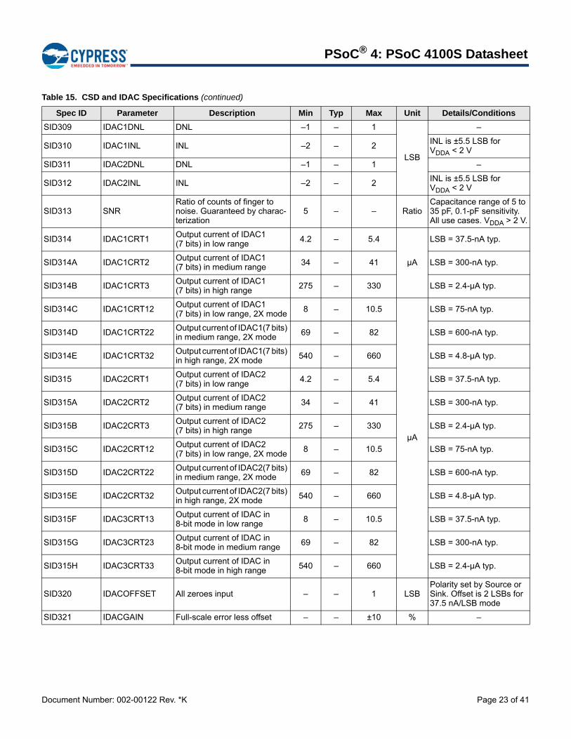
Document Number: 002-00122 Rev. *K Page 23 of 41
PSoC® 4: PSoC 4100S Datasheet
SID309 IDAC1DNL DNL –1 – 1
LSB
–
SID310 IDAC1INL INL –2 – 2INL is ±5.5 LSB forVDDA < 2 V
SID311 IDAC2DNL DNL –1 – 1 –
SID312 IDAC2INL INL –2 – 2 INL is ±5.5 LSB for VDDA < 2 V
SID313 SNRRatio of counts of finger to noise. Guaranteed by charac-terization
5 – – RatioCapacitance range of 5 to 35 pF, 0.1-pF sensitivity. All use cases. VDDA > 2 V.
SID314 IDAC1CRT1 Output current of IDAC1 (7 bits) in low range
4.2 – 5.4
µA
LSB = 37.5-nA typ.
SID314A IDAC1CRT2 Output current of IDAC1(7 bits) in medium range 34 – 41 LSB = 300-nA typ.
SID314B IDAC1CRT3Output current of IDAC1(7 bits) in high range 275 – 330 LSB = 2.4-µA typ.
SID314C IDAC1CRT12 Output current of IDAC1 (7 bits) in low range, 2X mode
8 – 10.5
µA
LSB = 75-nA typ.
SID314D IDAC1CRT22 Output current of IDAC1(7 bits) in medium range, 2X mode 69 – 82 LSB = 600-nA typ.
SID314E IDAC1CRT32Output current of IDAC1(7 bits) in high range, 2X mode 540 – 660 LSB = 4.8-µA typ.
SID315 IDAC2CRT1 Output current of IDAC2 (7 bits) in low range
4.2 – 5.4 LSB = 37.5-nA typ.
SID315A IDAC2CRT2 Output current of IDAC2 (7 bits) in medium range 34 – 41 LSB = 300-nA typ.
SID315B IDAC2CRT3Output current of IDAC2 (7 bits) in high range 275 – 330 LSB = 2.4-µA typ.
SID315C IDAC2CRT12 Output current of IDAC2 (7 bits) in low range, 2X mode
8 – 10.5 LSB = 75-nA typ.
SID315D IDAC2CRT22 Output current of IDAC2(7 bits) in medium range, 2X mode 69 – 82 LSB = 600-nA typ.
SID315E IDAC2CRT32Output current of IDAC2(7 bits) in high range, 2X mode 540 – 660 LSB = 4.8-µA typ.
SID315F IDAC3CRT13 Output current of IDAC in 8-bit mode in low range
8 – 10.5 LSB = 37.5-nA typ.
SID315G IDAC3CRT23 Output current of IDAC in 8-bit mode in medium range 69 – 82 LSB = 300-nA typ.
SID315H IDAC3CRT33Output current of IDAC in 8-bit mode in high range 540 – 660 LSB = 2.4-µA typ.
SID320 IDACOFFSET All zeroes input – – 1 LSBPolarity set by Source or Sink. Offset is 2 LSBs for 37.5 nA/LSB mode
SID321 IDACGAIN Full-scale error less offset – – ±10 % –
Table 15. CSD and IDAC Specifications (continued)
Spec ID Parameter Description Min Typ Max Unit Details/Conditions
Document Number: 002-00122 Rev. *K Page 24 of 41
PSoC® 4: PSoC 4100S Datasheet
SID322 IDACMISMATCH1 Mismatch between IDAC1 and IDAC2 in Low mode
– – 9.2
LSB
LSB = 37.5-nA typ.
SID322A IDACMISMATCH2 Mismatch between IDAC1 and IDAC2 in Medium mode
– – 5.6 LSB = 300-nA typ.
SID322B IDACMISMATCH3 Mismatch between IDAC1 and IDAC2 in High mode – – 6.8 LSB = 2.4-µA typ.
SID323 IDACSET8Settling time to 0.5 LSB for 8-bit IDAC – – 10
µs
Full-scale transition. No external load.
SID324 IDACSET7 Settling time to 0.5 LSB for 7-bit IDAC
– – 10 Full-scale transition. No external load.
SID325 CMOD External modulator capacitor. – 2.2 – nF 5-V rating, X7R or NP0 cap.
Table 15. CSD and IDAC Specifications (continued)
Spec ID Parameter Description Min Typ Max Unit Details/Conditions
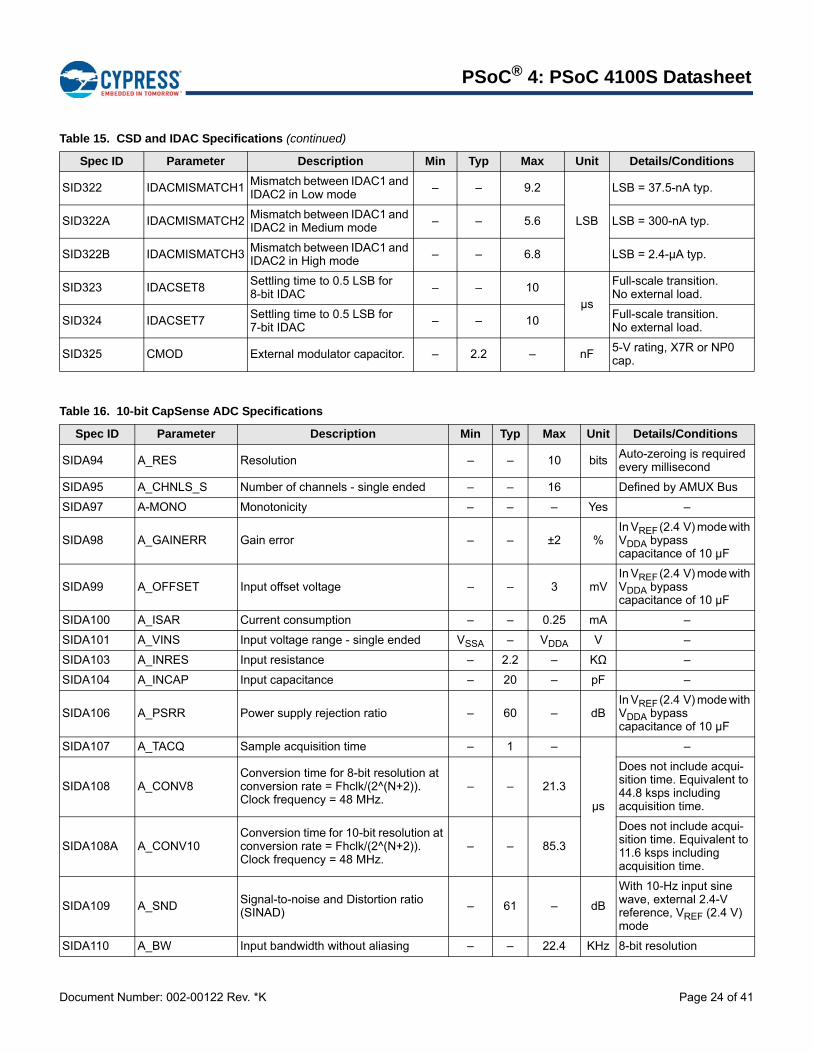
Table 16. 10-bit CapSense ADC Specifications
Spec ID Parameter Description Min Typ Max Unit Details/Conditions
SIDA94 A_RES Resolution – – 10 bits Auto-zeroing is required every millisecond
SIDA95 A_CHNLS_S Number of channels - single ended – – 16 Defined by AMUX Bus
SIDA97 A-MONO Monotonicity – – – Yes –
SIDA98 A_GAINERR Gain error – – ±2 %In VREF (2.4 V) mode with VDDA bypass capacitance of 10 µF
SIDA99 A_OFFSET Input offset voltage – – 3 mVIn VREF (2.4 V) mode with VDDA bypass capacitance of 10 µF
SIDA100 A_ISAR Current consumption – – 0.25 mA –
SIDA101 A_VINS Input voltage range - single ended VSSA – VDDA V –
SIDA103 A_INRES Input resistance – 2.2 – KΩ –
SIDA104 A_INCAP Input capacitance – 20 – pF –
SIDA106 A_PSRR Power supply rejection ratio – 60 – dBIn VREF (2.4 V) mode with VDDA bypass capacitance of 10 µF
SIDA107 A_TACQ Sample acquisition time – 1 –
µs
–
SIDA108 A_CONV8Conversion time for 8-bit resolution at conversion rate = Fhclk/(2^(N+2)). Clock frequency = 48 MHz.
– – 21.3
Does not include acqui-sition time. Equivalent to 44.8 ksps including acquisition time.
SIDA108A A_CONV10Conversion time for 10-bit resolution at conversion rate = Fhclk/(2^(N+2)). Clock frequency = 48 MHz.
– – 85.3
Does not include acqui-sition time. Equivalent to 11.6 ksps including acquisition time.
SIDA109 A_SND Signal-to-noise and Distortion ratio (SINAD) – 61 – dB
With 10-Hz input sine wave, external 2.4-V reference, VREF (2.4 V) mode
SIDA110 A_BW Input bandwidth without aliasing – – 22.4 KHz 8-bit resolution
Document Number: 002-00122 Rev. *K Page 25 of 41
PSoC® 4: PSoC 4100S Datasheet
Digital Peripherals
Timer Counter Pulse-Width Modulator (TCPWM)
I2C
SIDA111 A_INL Integral Non Linearity. 1 ksps – – 2LSB
VREF = 2.4 V or greater
SIDA112 A_DNL Differential Non Linearity. 1 ksps – – 1 –
Table 16. 10-bit CapSense ADC Specifications (continued)
Spec ID Parameter Description Min Typ Max Unit Details/Conditions
Table 17. TCPWM Specifications
Spec ID Parameter Description Min Typ Max Unit Details/Conditions
SID.TCPWM.1 ITCPWM1 Block current consumption at 3 MHz – – 45
μA All modes (TCPWM)SID.TCPWM.2 ITCPWM2 Block current consumption at 12 MHz – – 155SID.TCPWM.2A ITCPWM3 Block current consumption at 48 MHz – – 650
SID.TCPWM.3 TCPWMFREQ Operating frequency – – Fc MHz Fc max = CLK_SYSMaximum = 48 MHz
SID.TCPWM.4 TPWMENEXT Input trigger pulse width 2/Fc – –
ns
For all trigger events[6]
SID.TCPWM.5 TPWMEXT Output trigger pulse widths 2/Fc – –
Minimum possible width of Overflow, Underflow, and CC (Counter equals Compare value) outputs
SID.TCPWM.5A TCRES Resolution of counter 1/Fc – – Minimum time between successive counts
SID.TCPWM.5B PWMRES PWM resolution 1/Fc – – Minimum pulse width of PWM Output
SID.TCPWM.5C QRES Quadrature inputs resolution 1/Fc – –Minimum pulse width between Quadrature phase inputs
Notes6. Trigger events can be Stop, Start, Reload, Count, Capture, or Kill depending on which mode of operation is selected.7. Guaranteed by characterization.
Table 18. Fixed I2C DC Specifications[7]
Spec ID Parameter Description Min Typ Max Unit Details/Conditions
SID149 II2C1 Block current consumption at 100 kHz – – 50
µA
–
SID150 II2C2 Block current consumption at 400 kHz – – 135 –
SID151 II2C3 Block current consumption at 1 Mbps – – 310 –
SID152 II2C4 I2C enabled in Deep Sleep mode – – 1.4
Table 19. Fixed I2C AC Specifications[7]
Spec ID Parameter Description Min Typ Max Unit Details/Conditions
SID153 FI2C1 Bit rate – – 1 Msps –
Table 20. SPI DC Specifications[7]
Spec ID Parameter Description Min Typ Max Unit Details/Conditions
SID163 ISPI1 Block current consumption at 1 Mbps – – 360
µA
–
SID164 ISPI2 Block current consumption at 4 Mbps – – 560 –
SID165 ISPI3 Block current consumption at 8 Mbps – – 600 –
Document Number: 002-00122 Rev. *K Page 26 of 41
PSoC® 4: PSoC 4100S Datasheet
Note8. Guaranteed by characterization.
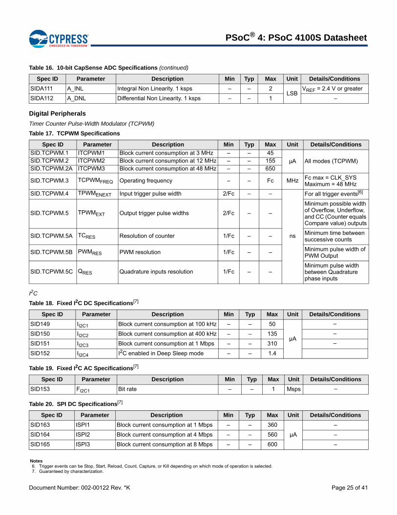
Table 21. SPI AC Specifications[8]
Spec ID Parameter Description Min Typ Max Unit Details/Conditions
SID166 FSPISPI Operating frequency (Master; 6X Oversampling) – – 8 MHz SID166
Fixed SPI Master Mode AC Specifications
SID167 TDMO MOSI Valid after SClock driving edge – – 15
ns
–
SID168 TDSIMISO Valid before SClock capturing edge 20 – –
Full clock, late MISO sampling
SID169 THMO Previous MOSI data hold time 0 – – Referred to Slave capturing edge
Fixed SPI Slave Mode AC Specifications
SID170 TDMI MOSI Valid before Sclock Capturing edge 40 – –
ns
–
SID171 TDSO MISO Valid after Sclock driving edge – –42 +
3*Tcpu TCPU = 1/FCPU
SID171A TDSO_EXT MISO Valid after Sclock driving edge in Ext. Clk mode
– – 48 –
SID172 THSO Previous MISO data hold time 0 – – –
SID172A TSSELSSCK SSEL Valid to first SCK Valid edge – – 100 –
Table 22. UART DC Specifications[8]
Spec ID Parameter Description Min Typ Max Unit Details/Conditions
SID160 IUART1Block current consumption at 100 Kbps – – 55
µA–
SID161 IUART2Block current consumption at 1000 Kbps
– – 312 –
Table 23. UART AC Specifications[8]
Spec ID Parameter Description Min Typ Max Unit Details/Conditions
SID162 FUART Bit rate – – 1 Mbps –
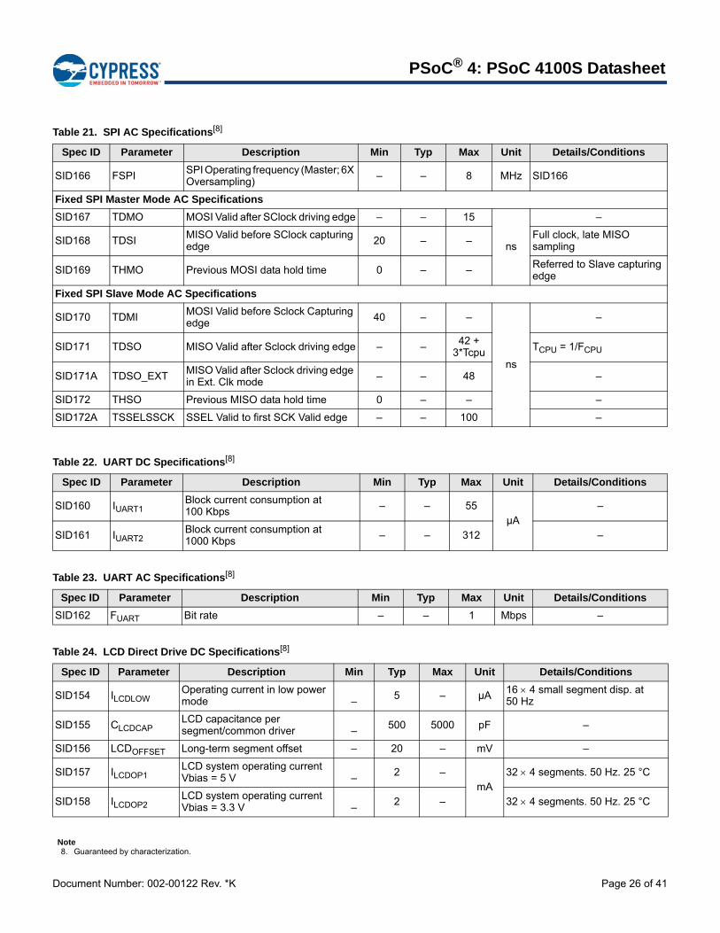
Table 24. LCD Direct Drive DC Specifications[8]
Spec ID Parameter Description Min Typ Max Unit Details/Conditions
SID154 ILCDLOWOperating current in low power mode – 5 – µA 16 4 small segment disp. at
50 Hz
SID155 CLCDCAPLCD capacitance per segment/common driver – 500 5000 pF –
SID156 LCDOFFSET Long-term segment offset – 20 – mV –
SID157 ILCDOP1LCD system operating current Vbias = 5 V – 2 –
mA32 4 segments. 50 Hz. 25 °C
SID158 ILCDOP2LCD system operating current Vbias = 3.3 V –
2 – 32 4 segments. 50 Hz. 25 °C
Document Number: 002-00122 Rev. *K Page 27 of 41
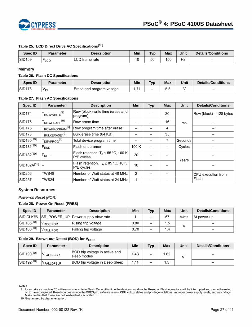
PSoC® 4: PSoC 4100S Datasheet
Memory
System Resources
Power-on Reset (POR)
Table 25. LCD Direct Drive AC Specifications[10]
Spec ID Parameter Description Min Typ Max Unit Details/Conditions
SID159 FLCD LCD frame rate 10 50 150 Hz –
Table 26. Flash DC Specifications
Spec ID Parameter Description Min Typ Max Unit Details/Conditions
SID173 VPE Erase and program voltage 1.71 – 5.5 V –
Table 27. Flash AC Specifications
Spec ID Parameter Description Min Typ Max Unit Details/Conditions
SID174 TROWWRITE[9] Row (block) write time (erase and
program) – – 20
ms
Row (block) = 128 bytes
SID175 TROWERASE[9] Row erase time – – 16 –
SID176 TROWPROGRAM[9] Row program time after erase – – 4 –
SID178 TBULKERASE[9] Bulk erase time (64 KB) – – 35 –
SID180[10] TDEVPROG[9] Total device program time – – 7 Seconds –
SID181[10] FEND Flash endurance 100 K – – Cycles –
SID182[10] FRETFlash retention. TA 55 °C, 100 K P/E cycles 20 – –
Years–
SID182A[10] – Flash retention. TA 85 °C, 10 K P/E cycles
10 – – –
SID256 TWS48 Number of Wait states at 48 MHz 2 – – CPU execution from FlashSID257 TWS24 Number of Wait states at 24 MHz 1 – –
Notes9. It can take as much as 20 milliseconds to write to Flash. During this time the device should not be Reset, or Flash operations will be interrupted and cannot be relied
on to have completed. Reset sources include the XRES pin, software resets, CPU lockup states and privilege violations, improper power supply levels, and watchdogs. Make certain that these are not inadvertently activated.
10. Guaranteed by characterization.
Table 28. Power On Reset (PRES)
Spec ID Parameter Description Min Typ Max Unit Details/Conditions
SID.CLK#6 SR_POWER_UP Power supply slew rate 1 – 67 V/ms At power-up
SID185[10] VRISEIPOR Rising trip voltage 0.80 – 1.5V
–
SID186[10] VFALLIPOR Falling trip voltage 0.70 – 1.4 –
Table 29. Brown-out Detect (BOD) for VCCD
Spec ID Parameter Description Min Typ Max Unit Details/Conditions
SID190[10] VFALLPPORBOD trip voltage in active and sleep modes 1.48 – 1.62
V–
SID192[10] VFALLDPSLP BOD trip voltage in Deep Sleep 1.11 – 1.5 –
Document Number: 002-00122 Rev. *K Page 28 of 41
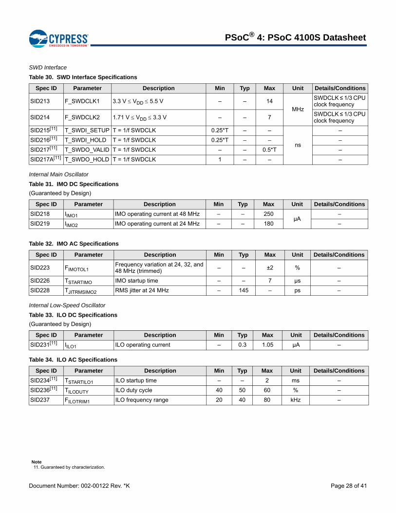
PSoC® 4: PSoC 4100S Datasheet
SWD Interface
Internal Main Oscillator
Internal Low-Speed Oscillator
Note11. Guaranteed by characterization.
Table 30. SWD Interface Specifications
Spec ID Parameter Description Min Typ Max Unit Details/Conditions
SID213 F_SWDCLK1 3.3 V VDD 5.5 V – – 14MHz
SWDCLK ≤ 1/3 CPU clock frequency
SID214 F_SWDCLK2 1.71 V VDD 3.3 V – – 7 SWDCLK ≤ 1/3 CPU clock frequency
SID215[11] T_SWDI_SETUP T = 1/f SWDCLK 0.25*T – –
ns
–
SID216[11] T_SWDI_HOLD T = 1/f SWDCLK 0.25*T – – –
SID217[11] T_SWDO_VALID T = 1/f SWDCLK – – 0.5*T –
SID217A[11] T_SWDO_HOLD T = 1/f SWDCLK 1 – – –
Table 31. IMO DC Specifications
(Guaranteed by Design)
Spec ID Parameter Description Min Typ Max Unit Details/Conditions
SID218 IIMO1 IMO operating current at 48 MHz – – 250µA
–
SID219 IIMO2 IMO operating current at 24 MHz – – 180 –
Table 32. IMO AC Specifications
Spec ID Parameter Description Min Typ Max Unit Details/Conditions
SID223 FIMOTOL1Frequency variation at 24, 32, and 48 MHz (trimmed) – – ±2 % –
SID226 TSTARTIMO IMO startup time – – 7 µs –
SID228 TJITRMSIMO2 RMS jitter at 24 MHz – 145 – ps –
Table 33. ILO DC Specifications
(Guaranteed by Design)
Spec ID Parameter Description Min Typ Max Unit Details/Conditions
SID231[11] IILO1 ILO operating current – 0.3 1.05 µA –
Table 34. ILO AC Specifications
Spec ID Parameter Description Min Typ Max Unit Details/Conditions
SID234[11] TSTARTILO1 ILO startup time – – 2 ms –
SID236[11] TILODUTY ILO duty cycle 40 50 60 % –
SID237 FILOTRIM1 ILO frequency range 20 40 80 kHz –
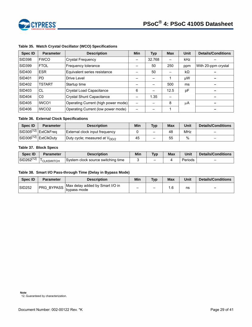
Document Number: 002-00122 Rev. *K Page 29 of 41
PSoC® 4: PSoC 4100S Datasheet
Note12. Guaranteed by characterization.
Table 35. Watch Crystal Oscillator (WCO) Specifications
Spec ID Parameter Description Min Typ Max Unit Details/Conditions
SID398 FWCO Crystal Frequency – 32.768 – kHz –
SID399 FTOL Frequency tolerance – 50 250 ppm With 20-ppm crystal
SID400 ESR Equivalent series resistance – 50 – kΩ –
SID401 PD Drive Level – – 1 µW –
SID402 TSTART Startup time – – 500 ms –
SID403 CL Crystal Load Capacitance 6 – 12.5 pF –
SID404 C0 Crystal Shunt Capacitance – 1.35 – –
SID405 IWCO1 Operating Current (high power mode) – – 8 A –
SID406 IWCO2 Operating Current (low power mode) – – 1 –
Table 36. External Clock Specifications
Spec ID Parameter Description Min Typ Max Unit Details/Conditions
SID305[12] ExtClkFreq External clock input frequency 0 – 48 MHz –
SID306[12] ExtClkDuty Duty cycle; measured at VDD/2 45 – 55 % –
Table 37. Block Specs
Spec ID Parameter Description Min Typ Max Unit Details/Conditions
SID262[12] TCLKSWITCH System clock source switching time 3 – 4 Periods –
Table 38. Smart I/O Pass-through Time (Delay in Bypass Mode)
Spec ID Parameter Description Min Typ Max Unit Details/Conditions
SID252 PRG_BYPASS Max delay added by Smart I/O in bypass mode – – 1.6 ns –
Document Number: 002-00122 Rev. *K Page 30 of 41
PSoC® 4: PSoC 4100S Datasheet
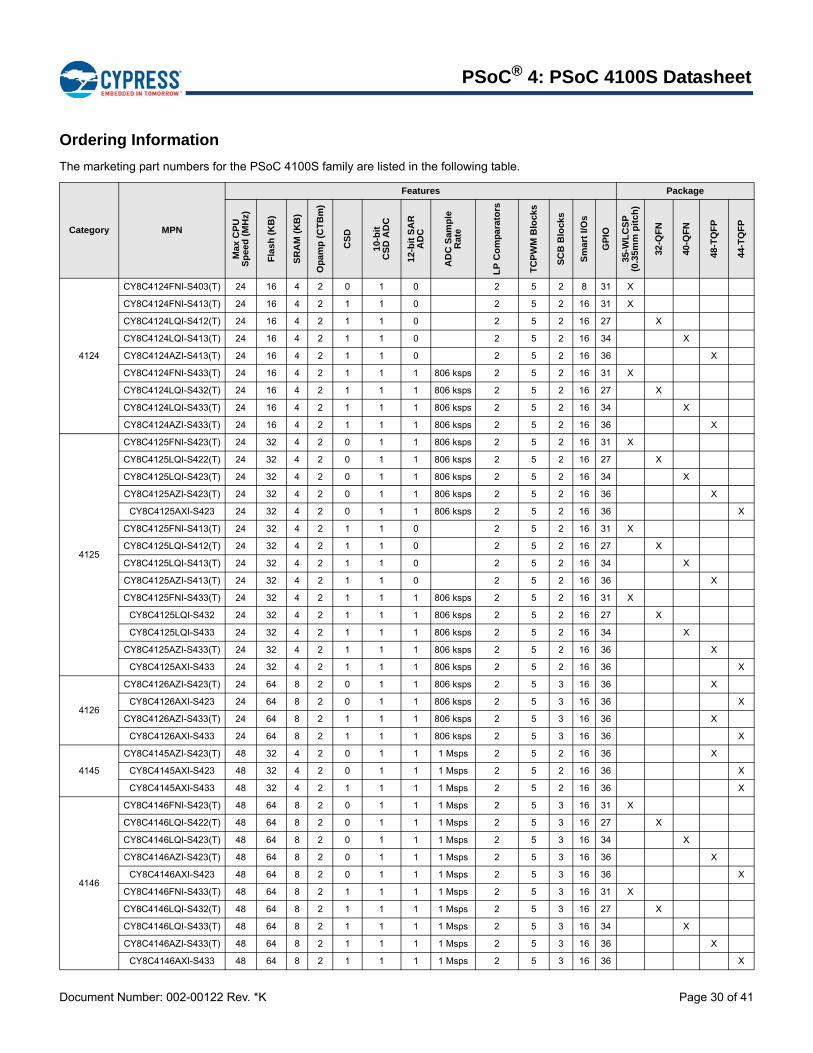
Ordering Information
The marketing part numbers for the PSoC 4100S family are listed in the following table.
Category MPN
Features Package
Ma
x C
PU
S
pe
ed
(M
Hz)
Fla
sh
(K
B)
SR
AM
(K
B)
Op
amp
(C
TB
m)
CS
D
10
-bit
C
SD
AD
C
12
-bit
SA
R
AD
C
AD
C S
amp
le
Rat
e
LP
Co
mp
ara
tors
TC
PW
M B
lock
s
SC
B B
lock
s
Sm
art
I/O
s
GP
IO
35
-WL
CS
P
(0.3
5mm
pit
ch
)
32-Q
FN
40-Q
FN
48
-TQ
FP
44
-TQ
FP
4124
CY8C4124FNI-S403(T) 24 16 4 2 0 1 0 2 5 2 8 31 X
CY8C4124FNI-S413(T) 24 16 4 2 1 1 0 2 5 2 16 31 X
CY8C4124LQI-S412(T) 24 16 4 2 1 1 0 2 5 2 16 27 X
CY8C4124LQI-S413(T) 24 16 4 2 1 1 0 2 5 2 16 34 X
CY8C4124AZI-S413(T) 24 16 4 2 1 1 0 2 5 2 16 36 X
CY8C4124FNI-S433(T) 24 16 4 2 1 1 1 806 ksps 2 5 2 16 31 X
CY8C4124LQI-S432(T) 24 16 4 2 1 1 1 806 ksps 2 5 2 16 27 X
CY8C4124LQI-S433(T) 24 16 4 2 1 1 1 806 ksps 2 5 2 16 34 X
CY8C4124AZI-S433(T) 24 16 4 2 1 1 1 806 ksps 2 5 2 16 36 X
4125
CY8C4125FNI-S423(T) 24 32 4 2 0 1 1 806 ksps 2 5 2 16 31 X
CY8C4125LQI-S422(T) 24 32 4 2 0 1 1 806 ksps 2 5 2 16 27 X
CY8C4125LQI-S423(T) 24 32 4 2 0 1 1 806 ksps 2 5 2 16 34 X
CY8C4125AZI-S423(T) 24 32 4 2 0 1 1 806 ksps 2 5 2 16 36 X
CY8C4125AXI-S423 24 32 4 2 0 1 1 806 ksps 2 5 2 16 36 X
CY8C4125FNI-S413(T) 24 32 4 2 1 1 0 2 5 2 16 31 X
CY8C4125LQI-S412(T) 24 32 4 2 1 1 0 2 5 2 16 27 X
CY8C4125LQI-S413(T) 24 32 4 2 1 1 0 2 5 2 16 34 X
CY8C4125AZI-S413(T) 24 32 4 2 1 1 0 2 5 2 16 36 X
CY8C4125FNI-S433(T) 24 32 4 2 1 1 1 806 ksps 2 5 2 16 31 X
CY8C4125LQI-S432 24 32 4 2 1 1 1 806 ksps 2 5 2 16 27 X
CY8C4125LQI-S433 24 32 4 2 1 1 1 806 ksps 2 5 2 16 34 X
CY8C4125AZI-S433(T) 24 32 4 2 1 1 1 806 ksps 2 5 2 16 36 X
CY8C4125AXI-S433 24 32 4 2 1 1 1 806 ksps 2 5 2 16 36 X
4126
CY8C4126AZI-S423(T) 24 64 8 2 0 1 1 806 ksps 2 5 3 16 36 X
CY8C4126AXI-S423 24 64 8 2 0 1 1 806 ksps 2 5 3 16 36 X
CY8C4126AZI-S433(T) 24 64 8 2 1 1 1 806 ksps 2 5 3 16 36 X
CY8C4126AXI-S433 24 64 8 2 1 1 1 806 ksps 2 5 3 16 36 X
4145
CY8C4145AZI-S423(T) 48 32 4 2 0 1 1 1 Msps 2 5 2 16 36 X
CY8C4145AXI-S423 48 32 4 2 0 1 1 1 Msps 2 5 2 16 36 X
CY8C4145AXI-S433 48 32 4 2 1 1 1 1 Msps 2 5 2 16 36 X
4146
CY8C4146FNI-S423(T) 48 64 8 2 0 1 1 1 Msps 2 5 3 16 31 X
CY8C4146LQI-S422(T) 48 64 8 2 0 1 1 1 Msps 2 5 3 16 27 X
CY8C4146LQI-S423(T) 48 64 8 2 0 1 1 1 Msps 2 5 3 16 34 X
CY8C4146AZI-S423(T) 48 64 8 2 0 1 1 1 Msps 2 5 3 16 36 X
CY8C4146AXI-S423 48 64 8 2 0 1 1 1 Msps 2 5 3 16 36 X
CY8C4146FNI-S433(T) 48 64 8 2 1 1 1 1 Msps 2 5 3 16 31 X
CY8C4146LQI-S432(T) 48 64 8 2 1 1 1 1 Msps 2 5 3 16 27 X
CY8C4146LQI-S433(T) 48 64 8 2 1 1 1 1 Msps 2 5 3 16 34 X
CY8C4146AZI-S433(T) 48 64 8 2 1 1 1 1 Msps 2 5 3 16 36 X
CY8C4146AXI-S433 48 64 8 2 1 1 1 1 Msps 2 5 3 16 36 X
Document Number: 002-00122 Rev. *K Page 31 of 41
PSoC® 4: PSoC 4100S Datasheet
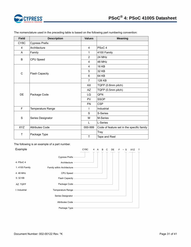
The nomenclature used in the preceding table is based on the following part numbering convention:
The following is an example of a part number.
Field Description Values Meaning
CY8C Cypress Prefix
4 Architecture 4 PSoC 4
A Family 1 4100 Family
B CPU Speed2 24 MHz
4 48 MHz
C Flash Capacity
4 16 KB
5 32 KB
6 64 KB
7 128 KB
DE Package Code
AX TQFP (0.8mm pitch)
AZ TQFP (0.5mm pitch)
LQ QFN
PV SSOP
FN CSP
F Temperature Range I Industrial
S Series Designator
S S-Series
M M-Series
L L-Series
XYZ Attributes Code 000-999 Code of feature set in the specific family
T Package TypeTray
T Tape and Reel
CY8C 4 – XYZ
Cypress Prefix
Architecture
Family within Architecture
CPU Speed
Temperature Range
Package Code
Flash Capacity
Attributes Code
Example
1: 4100 Family
Series Designator
4: PSoC 4
4: 48 MHz
5: 32 KB
AZ: TQFP
I: Industrial
A B C DE F S T
Package Type
Document Number: 002-00122 Rev. *K Page 32 of 41
PSoC® 4: PSoC 4100S Datasheet
Packaging
The PSoC 4100S will be offered in 48-pin TQFP, 44-pin TQFP, 40-pin QFN, 32-pin QFN, and 35-ball WLCSP packages.
Table 39 provides the package dimensions and Cypress drawing numbers.
Table 39. Package List
Spec ID Package Description Package Dwg
BID20 48-pin TQFP 7 × 7 × 1.4-mm height with 0.5-mm pitch 51-85135
BID20A 44-pin TQFP 10 × 10 × 1.6-mm height with 0.8-mm pitch 51-85064
BID27 40-pin QFN 6 × 6 × 0.6-mm height with 0.5-mm pitch 001-80659
BID34A 32-pin QFN 5 × 5 × 0.6-mm height with 0.5-mm pitch 001-42168
BID34D 35-ball WLCSP 2.6 × 2.1 × 0.48-mm height with 0.35-mm pitch 002-09958
Table 40. Package Thermal Characteristics
Parameter Description Package Min Typ Max Unit Details/Conditions
TA Operating ambient temperature – –40 25 85°C
–
TJ Operating junction temperature – –40 – 100 –
TJA Package θJA 48-pin TQFP – 74.8 –
°C/Watt
–
TJC Package θJC 48-pin TQFP – 35.7 – –
TJA Package θJA 44-pin TQFP – 57.2 – –
TJC Package θJC 44-pin TQFP – 17.5 – –
TJA Package θJA 40-pin QFN – 17.8 – –
TJC Package θJC 40-pin QFN – 2.8 – –
TJA Package θJA 32-pin QFN – 19.9 – –
TJC Package θJC 32-pin QFN – 4.3 – –
TJA Package θJA 35-ball WLCSP – 43 – –
TJC Package θJC 35-ball WLCSP – 0.3 – –
Table 41. Solder Reflow Peak Temperature
Package Maximum Peak Temperature Maximum Time at Peak Temperature
All 260 °C 30 seconds
Table 42. Package Moisture Sensitivity Level (MSL), IPC/JEDEC J-STD-020
Package MSL
All except WLCSP MSL 3
35-ball WLCSP MSL 1

Document Number: 002-00122 Rev. *K Page 33 of 41
PSoC® 4: PSoC 4100S Datasheet
Package Diagrams
Figure 7. 48-pin TQFP Package Outline
Figure 8. 44-pin TQFP Package Outline
51-85135 *C
51-85064 *G
Document Number: 002-00122 Rev. *K Page 34 of 41
PSoC® 4: PSoC 4100S Datasheet
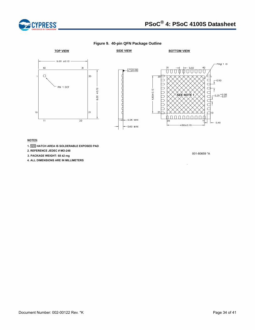
Figure 9. 40-pin QFN Package Outline
001-80659 *A
Document Number: 002-00122 Rev. *K Page 35 of 41
PSoC® 4: PSoC 4100S Datasheet
Figure 10. 32-pin QFN Package Outline
BOTTOM VIEW
TOP VIEW
SIDE VIEW
SEE NOTE 1
4. DIMENSIONS ARE IN MILLIMETERS
2. BASED ON REF JEDEC # MO-248
NOTES:
1. HATCH AREA IS SOLDERABLE EXPOSED PAD
3. PACKAGE WEIGHT: 0.0388g
DIMENSIONS
NOM.MIN.
b
E
D
A
A1 -
SYMBOLMAX.
0.60
0.045
0.50 TYP
L
0.18 0.25 0.30
E2
D2
e
0.400.30 0.50
3.40 3.50 3.60
A2 0.15 BSC
4.90 5.00 5.10
4.90 5.00 5.10
3.40 3.50 3.60
0.550.50
0.020
001-42168 *F
Document Number: 002-00122 Rev. *K Page 36 of 41
PSoC® 4: PSoC 4100S Datasheet
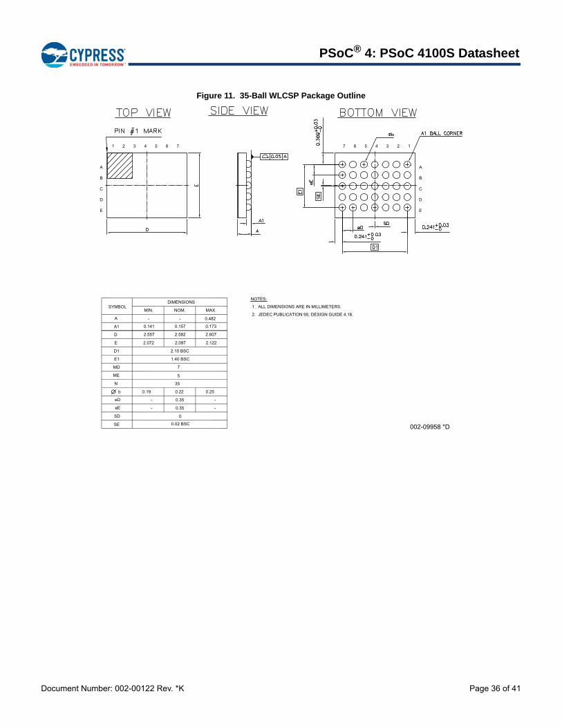
Figure 11. 35-Ball WLCSP Package Outline
7 6 5 4 3 2 1
E
D
C
B
A
7654321
E
D
C
B
A
JEDEC PUBLICATION 95; DESIGN GUIDE 4.18.
NOTES:
2.
1. ALL DIMENSIONS ARE IN MILLIMETERS.
SD
b
eE
eD
ME
N
0
35
5
DIMENSIONS
D1
MD
E1
E
D
A
A1
SYMBOLMIN.
-
2.10 BSC
1.40 BSC
7
2.097
2.582
NOM.
- 0.482
MAX.
SE 0.02 BSC
2.557 2.607
2.072 2.122
0.35- -
0.35- -
0.220.19 0.25
0.1570.141 0.173
002-09958 *D
Document Number: 002-00122 Rev. *K Page 37 of 41
PSoC® 4: PSoC 4100S Datasheet
Acronyms
Table 43. Acronyms Used in this Document
Acronym Description
abus analog local bus
ADC analog-to-digital converter
AG analog global
AHBAMBA (advanced microcontroller bus architecture) high-performance bus, an ARM data transfer bus
ALU arithmetic logic unit
AMUXBUS analog multiplexer bus
API application programming interface
APSR application program status register
ARM® advanced RISC machine, a CPU architecture
ATM automatic thump mode
BW bandwidth
CAN Controller Area Network, a communications protocol
CMRR common-mode rejection ratio
CPU central processing unit
CRC cyclic redundancy check, an error-checking protocol
DAC digital-to-analog converter, see also IDAC, VDAC
DFB digital filter block
DIOdigital input/output, GPIO with only digital capabilities, no analog. See GPIO.
DMIPS Dhrystone million instructions per second
DMA direct memory access, see also TD
DNL differential nonlinearity, see also INL
DNU do not use
DR port write data registers
DSI digital system interconnect
DWT data watchpoint and trace
ECC error correcting code
ECO external crystal oscillator
EEPROM electrically erasable programmable read-only memory
EMI electromagnetic interference
EMIF external memory interface
EOC end of conversion
EOF end of frame
EPSR execution program status register
ESD electrostatic discharge
ETM embedded trace macrocell
FIR finite impulse response, see also IIR
FPB flash patch and breakpoint
FS full-speed
GPIOgeneral-purpose input/output, applies to a PSoC pin
HVI high-voltage interrupt, see also LVI, LVD
IC integrated circuit
IDAC current DAC, see also DAC, VDAC
IDE integrated development environment
I2C, or IIC Inter-Integrated Circuit, a communications protocol
IIR infinite impulse response, see also FIR
ILO internal low-speed oscillator, see also IMO
IMO internal main oscillator, see also ILO
INL integral nonlinearity, see also DNL
I/O input/output, see also GPIO, DIO, SIO, USBIO
IPOR initial power-on reset
IPSR interrupt program status register
IRQ interrupt request
ITM instrumentation trace macrocell
LCD liquid crystal display
LIN Local Interconnect Network, a communications protocol.
LR link register
LUT lookup table
LVD low-voltage detect, see also LVI
LVI low-voltage interrupt, see also HVI
LVTTL low-voltage transistor-transistor logic
MAC multiply-accumulate
MCU microcontroller unit
MISO master-in slave-out
NC no connect
NMI nonmaskable interrupt
NRZ non-return-to-zero
NVIC nested vectored interrupt controller
NVL nonvolatile latch, see also WOL
opamp operational amplifier
PAL programmable array logic, see also PLD
Table 43. Acronyms Used in this Document (continued)
Acronym Description
Document Number: 002-00122 Rev. *K Page 38 of 41
PSoC® 4: PSoC 4100S Datasheet
PC program counter
PCB printed circuit board
PGA programmable gain amplifier
PHUB peripheral hub
PHY physical layer
PICU port interrupt control unit
PLA programmable logic array
PLD programmable logic device, see also PAL
PLL phase-locked loop
PMDD package material declaration data sheet
POR power-on reset
PRES precise power-on reset
PRS pseudo random sequence
PS port read data register
PSoC® Programmable System-on-Chip™
PSRR power supply rejection ratio
PWM pulse-width modulator
RAM random-access memory
RISC reduced-instruction-set computing
RMS root-mean-square
RTC real-time clock
RTL register transfer language
RTR remote transmission request
RX receive
SAR successive approximation register
SC/CT switched capacitor/continuous time
SCL I2C serial clock
SDA I2C serial data
S/H sample and hold
SINAD signal to noise and distortion ratio
SIOspecial input/output, GPIO with advanced features. See GPIO.
SOC start of conversion
SOF start of frame
SPISerial Peripheral Interface, a communications protocol
SR slew rate
SRAM static random access memory
SRES software reset
SWD serial wire debug, a test protocol
Table 43. Acronyms Used in this Document (continued)
Acronym Description
SWV single-wire viewer
TD transaction descriptor, see also DMA
THD total harmonic distortion
TIA transimpedance amplifier
TRM technical reference manual
TTL transistor-transistor logic
TX transmit
UARTUniversal Asynchronous Transmitter Receiver, a communications protocol
UDB universal digital block
USB Universal Serial Bus
USBIO USB input/output, PSoC pins used to connect to a USB port
VDAC voltage DAC, see also DAC, IDAC
WDT watchdog timer
WOL write once latch, see also NVL
WRES watchdog timer reset
XRES external reset I/O pin
XTAL crystal
Table 43. Acronyms Used in this Document (continued)
Acronym Description

Document Number: 002-00122 Rev. *K Page 39 of 41
PSoC® 4: PSoC 4100S Datasheet
Document Conventions
Units of Measure
Table 44. Units of Measure
Symbol Unit of Measure
°C degrees Celsius
dB decibel
fF femto farad
Hz hertz
KB 1024 bytes
kbps kilobits per second
Khr kilohour
kHz kilohertz
k kilo ohm
ksps kilosamples per second
LSB least significant bit
Mbps megabits per second
MHz megahertz
M mega-ohm
Msps megasamples per second
µA microampere
µF microfarad
µH microhenry
µs microsecond
µV microvolt
µW microwatt
mA milliampere
ms millisecond
mV millivolt
nA nanoampere
ns nanosecond
nV nanovolt
ohm
pF picofarad
ppm parts per million
ps picosecond
s second
sps samples per second
sqrtHz square root of hertz
V volt
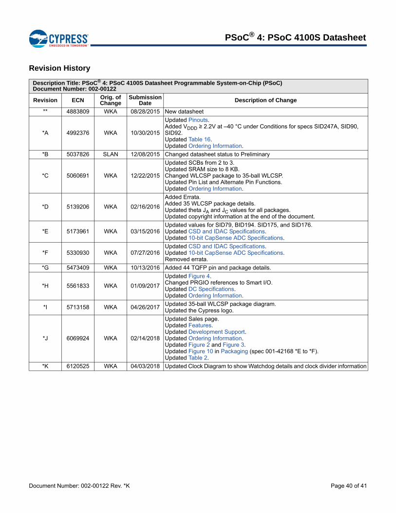
Document Number: 002-00122 Rev. *K Page 40 of 41
PSoC® 4: PSoC 4100S Datasheet
Revision History
Description Title: PSoC® 4: PSoC 4100S Datasheet Programmable System-on-Chip (PSoC)Document Number: 002-00122
Revision ECN Orig. of Change
Submission Date Description of Change
** 4883809 WKA 08/28/2015 New datasheet
*A 4992376 WKA 10/30/2015
Updated Pinouts.Added VDDD ≥ 2.2V at –40 °C under Conditions for specs SID247A, SID90, SID92.Updated Table 16.Updated Ordering Information.
*B 5037826 SLAN 12/08/2015 Changed datasheet status to Preliminary
*C 5060691 WKA 12/22/2015
Updated SCBs from 2 to 3.Updated SRAM size to 8 KB.Changed WLCSP package to 35-ball WLCSP.Updated Pin List and Alternate Pin Functions.Updated Ordering Information.
*D 5139206 WKA 02/16/2016
Added Errata.Added 35 WLCSP package details.Updated theta JA and JC values for all packages.Updated copyright information at the end of the document.
*E 5173961 WKA 03/15/2016Updated values for SID79, BID194. SID175, and SID176.Updated CSD and IDAC Specifications.Updated 10-bit CapSense ADC Specifications.
*F 5330930 WKA 07/27/2016Updated CSD and IDAC Specifications.Updated 10-bit CapSense ADC Specifications.Removed errata.
*G 5473409 WKA 10/13/2016 Added 44 TQFP pin and package details.
*H 5561833 WKA 01/09/2017
Updated Figure 4.Changed PRGIO references to Smart I/O.Updated DC Specifications.Updated Ordering Information.
*I 5713158 WKA 04/26/2017Updated 35-ball WLCSP package diagram.Updated the Cypress logo.
*J 6069924 WKA 02/14/2018
Updated Sales page.Updated Features.Updated Development Support.Updated Ordering Information.Updated Figure 2 and Figure 3.Updated Figure 10 in Packaging (spec 001-42168 *E to *F).Updated Table 2.
*K 6120525 WKA 04/03/2018 Updated Clock Diagram to show Watchdog details and clock divider information
Document Number: 002-00122 Rev. *K Revised April 3, 2018 Page 41 of 41
© Cypress Semiconductor Corporation, 2015-2018. This document is the property of Cypress Semiconductor Corporation and its subsidiaries, including Spansion LLC ("Cypress"). This document,including any software or firmware included or referenced in this document ("Software"), is owned by Cypress under the intellectual property laws and treaties of the United States and other countriesworldwide. Cypress reserves all rights under such laws and treaties and does not, except as specifically stated in this paragraph, grant any license under its patents, copyrights, trademarks, or otherintellectual property rights. If the Software is not accompanied by a license agreement and you do not otherwise have a written agreement with Cypress governing the use of the Software, then Cypresshereby grants you a personal, non-exclusive, nontransferable license (without the right to sublicense) (1) under its copyright rights in the Software (a) for Software provided in source code form, tomodify and reproduce the Software solely for use with Cypress hardware products, only internally within your organization, and (b) to distribute the Software in binary code form externally to end users(either directly or indirectly through resellers and distributors), solely for use on Cypress hardware product units, and (2) under those claims of Cypress's patents that are infringed by the Software (asprovided by Cypress, unmodified) to make, use, distribute, and import the Software solely for use with Cypress hardware products. Any other use, reproduction, modification, translation, or compilationof the Software is prohibited.
TO THE EXTENT PERMITTED BY APPLICABLE LAW, CYPRESS MAKES NO WARRANTY OF ANY KIND, EXPRESS OR IMPLIED, WITH REGARD TO THIS DOCUMENT OR ANY SOFTWAREOR ACCOMPANYING HARDWARE, INCLUDING, BUT NOT LIMITED TO, THE IMPLIED WARRANTIES OF MERCHANTABILITY AND FITNESS FOR A PARTICULAR PURPOSE. No computingdevice can be absolutely secure. Therefore, despite security measures implemented in Cypress hardware or software products, Cypress does not assume any liability arising out of any security breach,such as unauthorized access to or use of a Cypress product. In addition, the products described in these materials may contain design defects or errors known as errata which may cause the productto deviate from published specifications. To the extent permitted by applicable law, Cypress reserves the right to make changes to this document without further notice. Cypress does not assume anyliability arising out of the application or use of any product or circuit described in this document. Any information provided in this document, including any sample design information or programmingcode, is provided only for reference purposes. It is the responsibility of the user of this document to properly design, program, and test the functionality and safety of any application made of thisinformation and any resulting product. Cypress products are not designed, intended, or authorized for use as critical components in systems designed or intended for the operation of weapons, weaponssystems, nuclear installations, life-support devices or systems, other medical devices or systems (including resuscitation equipment and surgical implants), pollution control or hazardous substancesmanagement, or other uses where the failure of the device or system could cause personal injury, death, or property damage ("Unintended Uses"). A critical component is any component of a deviceor system whose failure to perform can be reasonably expected to cause the failure of the device or system, or to affect its safety or effectiveness. Cypress is not liable, in whole or in part, and youshall and hereby do release Cypress from any claim, damage, or other liability arising from or related to all Unintended Uses of Cypress products. You shall indemnify and hold Cypress harmless fromand against all claims, costs, damages, and other liabilities, including claims for personal injury or death, arising from or related to any Unintended Uses of Cypress products.
Cypress, the Cypress logo, Spansion, the Spansion logo, and combinations thereof, WICED, PSoC, CapSense, EZ-USB, F-RAM, and Traveo are trademarks or registered trademarks of Cypress inthe United States and other countries. For a more complete list of Cypress trademarks, visit cypress.com. Other names and brands may be claimed as property of their respective owners.
PSoC® 4: PSoC 4100S Datasheet
Sales, Solutions, and Legal Information
Worldwide Sales and Design Support
Cypress maintains a worldwide network of offices, solution centers, manufacturer’s representatives, and distributors. To find the office closest to you, visit us at Cypress Locations.
Products
Arm® Cortex® Microcontrollers cypress.com/arm
Automotive cypress.com/automotive
Clocks & Buffers cypress.com/clocks
Interface cypress.com/interface
Internet of Things cypress.com/iot
Memory cypress.com/memory
Microcontrollers cypress.com/mcu
PSoC cypress.com/psoc
Power Management ICs cypress.com/pmic
Touch Sensing cypress.com/touch
USB Controllers cypress.com/usb
Wireless Connectivity cypress.com/wireless
PSoC® Solutions
PSoC 1 | PSoC 3 | PSoC 4 | PSoC 5LP | PSoC 6 MCU
Cypress Developer Community
Community | Projects | Video | Blogs | Training | Components
Technical Support
cypress.com/support