Embed Size (px)
Citation preview

www.cypress.com Document No. 001-88619 Rev. *E 1
AN88619
PSoC® 4 Hardware Design Considerations
Author: Johnny Zhang
Associated Part Family: PSoC 4
Related Documentation: For a complete list, click here.
To get the latest version of this application note, or the associated project file, please visit http://www.cypress.com/go/AN88619.
AN88619 shows you how to design a hardware system around a PSoC® 4 device, starting with considerations for
package selection, power, clocking, reset, I/O usage, programming and debugging interfaces, and analog module
design.
Contents
1 Introduction ............................................................... 1 2 PSoC Resources ...................................................... 2
2.1 PSoC Creator .................................................. 2 2.2 Code Examples ............................................... 3 2.3 PSoC Creator Help .......................................... 4 2.4 Technical Support ............................................ 4
3 Package Selection .................................................... 4 4 Power ....................................................................... 5
4.1 Power Pin Connections ................................... 6 4.2 Power Ramp-Up Considerations ..................... 7 4.3 PSoC Creator Settings for Device Power ........ 8 4.4 Thermal Considerations ................................... 8
5 Clocking .................................................................... 9 6 Reset ...................................................................... 10 7 Programming and Debugging ................................. 10 8 GPIO Pins............................................................... 11
8.1 I/O Pin Selection ............................................ 11 8.2 Special Ports ................................................. 13
9 Component Placement ........................................... 15 10 Analog Module Design Tips .................................... 16
10.1 SAR ADC ....................................................... 16 10.2 Opamps ......................................................... 20 10.3 Comparators .................................................. 20 10.4 CapSense ...................................................... 21 10.5 Current DACs (IDACs) ................................... 21
11 Summary ................................................................ 22 12 Related Documents ................................................ 23 A Appendix A – PCB Layout Tips .............................. 24 B Appendix B – Family Hardware Resources
Look-Up Table ........................................................ 25 C Appendix C – Schematic Checklist ......................... 28 Worldwide Sales and Design Support ............................. 30
1 Introduction
PSoC 4 is a powerful, programmable microcontroller with an ARM® Cortex™-M0 CPU. It provides the capability and
flexibility for analog and digital applications beyond what traditional MCUs offer. Currently, PSoC 4 portfolio contains the following families: PSoC 4000, 4100, 4200, 4100M, 4200M, 4100L, 4200L and PSoC 4 BLE. For an overview and comparison of these device families see Appendix B – Family Hardware Resources Look-Up Table.
This application note discusses considerations for hardware design including package, power, clocking, reset, I/O use, programming, and debugging; and provides design tips for analog modules for these family of devices. It also discusses good board-layout techniques, which are particularly important for precision analog applications.
The PSoC 4 device must be configured to work in its hardware environment, which you can with the PSoC Creator integrated design environment (IDE). The example configuration shown in this application note is based on a PSoC 4200 device; configurations for the other devices should be similar.
This application note assumes that you have some basic familiarity with PSoC 4 devices and PSoC Creator. If you are new to PSoC 4, refer to AN79953 – Getting Started with PSoC 4. If you are new to PSoC Creator, see the PSoC Creator home page. PSoC 4 BLE related topics are covered in AN91267 - Getting Started with PSoC 4 BLE. For the PSoC 4 BLE family, there is an important topic for hardware design: BLE antenna design. As it involves specific RF expertise, we explore this topic in others application notes, please see related documents.

PSoC® 4 Hardware Design Considerations
www.cypress.com Document No. 001-88619 Rev. *E 2
2 PSoC Resources Cypress provides a wealth of data at www.cypress.com to help you to select the right PSoC device, and to help you to quickly and effectively integrate the device into your design. For a comprehensive list of resources, see KBA86521, How to Design with PSoC 3, PSoC 4, and PSoC 5LP. The following is an abbreviated list for PSoC 4:
Overview: PSoC Portfolio, PSoC Roadmap
Product Selectors: PSoC 1, PSoC 3,
PSoC 4, or PSoC 5LP. In addition, PSoC Creator includes a device selection tool.
Datasheets describe and provide electrical
specifications for the PSoC 4000, PSoC 4100, and PSoC 4200, PSoC 4xx7 BLE, PSoC 4100M and PSoC 4200M, PSoC 4200L device families
CapSense Design Guide: Learn how to
design capacitive touch-sensing applications with the PSoC 4 family of devices.
Application Notes and Code Examples
cover a broad range of topics, from basic to advanced level. Many of the application notes include code examples. PSoC Creator provides additional code examples – see Code Examples.
Technical Reference Manuals (TRM) provide
detailed descriptions of the architecture and registers in each PSoC 4 device family.
PSoC Training Videos: These videos provide
step-by-step instructions on how to get started build complex designs with PSoC.
Development Kits: CY8CKIT-040, CY8CKIT-042,
CY8CKIT-044, and CY8CKIT-046 PSoC 4 Pioneer Kits are easy-to-use and inexpensive development platforms. These kits include connectors for Arduino™ compatible shields and Digilent
®
Pmod™ daughter cards.
CY8CKIT-043 and CY8CKIT-049 are very low-cost prototyping platform for sampling PSoC 4200 devices.
The MiniProg3 device provides an interface for flash programming and debug.
2.1 PSoC Creator
PSoC Creator is a free Windows-based Integrated Development Environment (IDE). It enables concurrent hardware and firmware design of PSoC 3, PSoC 4, and PSoC 5LP systems. See Figure 1 – with PSoC Creator, you can:
1. Drag and drop Components to build your hardware system design in the main design workspace
2. Co-design your application firmware with the PSoC hardware
3. Configure Components using configuration tools
4. Explore the library of 100+ Components
5. Review Component datasheets
Figure 1. PSoC Creator Features

PSoC® 4 Hardware Design Considerations
www.cypress.com Document No. 001-88619 Rev. *E 3
2.2 Code Examples
PSoC Creator includes a large number of code example projects. These projects are available from the PSoC Creator Start Page, as shown in Figure 2.
Example projects can speed up your design process by starting you off with a complete design, instead of a blank page. The example projects also show how PSoC Creator Components can be used for various applications. Code examples and datasheets are included, as shown in Figure 3.
In the Find Example Project dialog shown in Figure 3, you have several options:
Filter for examples based on architecture or device family, i.e., PSoC 3, PSoC 4 or PSoC 5LP; category; or keyword
Select from the menu of examples offered based on the Filter Options
Review the datasheet for the selection (on the Documentation tab)
Review the code example for the selection. You can copy and paste code from this window to your project, which can help speed up code development, or
Create a new project (and a new workspace if needed) based on the selection. This can speed up your design process by starting you off with a complete, basic design. You can then adapt that design to your application.
Figure 2. Code Examples in PSoC Creator
Figure 3. Code Example Projects with Sample Code

PSoC® 4 Hardware Design Considerations
www.cypress.com Document No. 001-88619 Rev. *E 4
2.3 PSoC Creator Help
Visit the PSoC Creator home page to download the latest version of PSoC Creator. Then, launch PSoC Creator and navigate to the following items:
Quick Start Guide: Choose Help > Documentation > Quick Start Guide. This guide gives you the basics for
developing PSoC Creator projects.
Simple Component example projects: Choose File > Open > Example projects. These example projects
demonstrate how to configure and use PSoC Creator Components.
System Reference Guide: Choose Help > System Reference > System Reference Guide. This guide lists
and describes the system functions provided by PSoC Creator.
Component datasheets: Right-click a Component and select “Open Datasheet.” Visit the PSoC 4 Component
Datasheets page for a list of all PSoC 4 Component datasheets.
PSoC Creator Training Videos: These videos provide step-by-step instructions on how to get started with PSoC
Creator.
Document Manager: PSoC Creator provides a document manager to help you to easily find and review document resources. To open the document manager, choose the menu item Help > Document Manager.
2.4 Technical Support
If you have any questions, our technical support team is happy to assist you. You can create a support request on the Cypress Technical Support page.
If you are in the United States, you can talk to our technical support team by calling our toll-free number: +1-800-541-4736. Select option 8 at the prompt.
You can also use the following support resources if you need quick assistance.
Self-help
Local Sales Office Locations
3 Package Selection
One of the first decisions you must make for your PCB is the choice of package. Several considerations drive this decision, including the number of PSoC device pins required, PCB and product size, PCB design rules, and thermal and mechanical stability. PSoC 4 devices are available in the following packages with different characteristics.
SOIC (Small-Outline Integrated Circuit): This package type is evolved from DIP (Dual In-line Package). It has
two lines of pins, and is generally used for chips with a small number of pins (Less than 20). Because it has a very large pitch, it is easy to route signals and manually weld. It also provides a good mechanical stability.
TQFP (Thin Quad Flat Package): This package type makes it easy to route signals due to the large pitch and
the open area below the part. Disadvantages are a larger package size and lower mechanical stability.
SSOP (Shrink Small-Outline Package): This package type provides the same advantages and disadvantages
as the TQFP package.
QFN (Quad Flat No-lead): This package type is much smaller than the other two packages. The central
exposure pad gives the package the best heat dispersion performance and mechanical stability. Disadvantages are that it is more difficult to route signals due to the center pad. For more information, see AN72845 – Design Guidelines for QFN Packaged Devices.
WLCSP (Wafer Level Chip-Scale Package): This package type makes the chip size as small as the die. All pins
are led as balls underneath the package. The extremely tiny size of the package makes it a perfect option for the scenarios where the PCB room is critical, such as in portable applications. The disadvantage is that the package provides less mechanical stability than other packages.
PSoC® 4 Hardware Design Considerations
www.cypress.com Document No. 001-88619 Rev. *E 5
VFBGA (Very Fine-Pitch Ball Grid Array): This package type is used for devices with large number of I/Os, as
it provides a miniature package for more than hundreds of pins. The disadvantage is a low mechanical stability.
As a design reference, see PSoC 4 CAD Libraries , which contain PSoC 4 schematics and PCB libraries. Note that you may need to modify the libraries slightly when you use them in your hardware design. Cypress takes no responsibility for issues related to the use of the libraries.
4 Power
PSoC 4 can be powered by a single supply with a wide voltage range, from 1.71 V to 5.5 V. As listed in Table 1, it has separate power domains for analog and digital modules. VDDA is the analog power supply pin, VSSA is the analog ground pin, VDDD and VCCD are the digital power supply pins, VDDIO is the power supply pin for I/Os, VSS is the digital ground pin, and VDDR is the RF power pin.
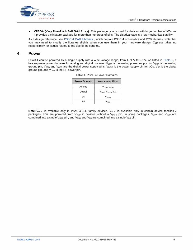
Table 1. PSoC 4 Power Domains
Power Domain Associated Pins
Analog VDDA, VSSA
Digital VDDD, VCCD, VSS
I/O VDDIO
RF VDDR
Note: VDDR is available only in PSoC 4 BLE family devices. VDDIO is available only in certain device families / packages. I/Os are powered from VDDD in devices without a VDDIO pin. In some packages, VDDA and VDDD are combined into a single VDDD pin, and VSSA and VSS are combined into a single VSS pin.
PSoC® 4 Hardware Design Considerations
www.cypress.com Document No. 001-88619 Rev. *E 6
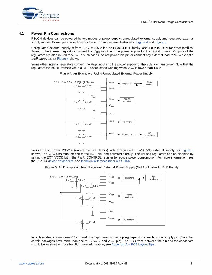
4.1 Power Pin Connections
PSoC 4 devices can be powered by two modes of power supply: unregulated external supply and regulated external supply modes. Power pin connections for these two modes are illustrated in Figure 4 and Figure 5.
Unregulated external supply is from 1.9 V to 5.5 V for the PSoC 4 BLE family, and 1.8 V to 5.5 V for other families. Some of the internal regulators convert the VDDD input into the power supply for the digital domain. Outputs of the regulators are also routed to VCCD. In such cases, do not power this pin or connect any external load to VCCD except a 1-μF capacitor, as Figure 4 shows.
Some other internal regulators convert the VDDR input into the power supply for the BLE RF transceiver. Note that the regulators for the RF transceiver in a BLE device stops working when VDDR is lower than 1.9 V.
Figure 4. An Example of Using Unregulated External Power Supply
VCCD
VDDD
VDDA
VSS
Digital
Modules
Analog
Modules
Regulators1.8 V – 5.5 V (1.9 V – 5.5 V for BLE Family)
I/O systemVDDIO
1 μF
VDDR RF
TransceiverRegulators
1 μF 0.1 μF
1 μF 0.1 μF
1 μF 0.1 μF
VSSA
1 μF 0.1 μF
You can also power PSoC 4 (except the BLE family) with a regulated 1.8-V (±5%) external supply, as Figure 5 shows. The VCCD pins must be tied to the VDDD pin, and powered directly. The unused regulators can be disabled by setting the EXT_VCCD bit in the PWR_CONTROL register to reduce power consumption. For more information, see the PSoC 4 device datasheets, and technical reference manuals (TRM).
Figure 5. An Example of Using Regulated External Power Supply (Not Applicable for BLE Family)
VCCD
VDDD
VDDA
VSS
Digital
Modules
Analog
Modules
Regulators1.71 V – 1.89 V (1.8 V ± 5%)
I/O systemVDDIO
1 μF 0.1 μF
VSSA
1 μF 0.1 μF
1 μF 0.1 μF
1 μF 0.1 μF
In both modes, connect one 0.1-μF and one 1-μF ceramic decoupling capacitor to each power supply pin (Note that certain packages have more than one VDDD, VDDA, and VDDIO pin). The PCB trace between the pin and the capacitors should be as short as possible. For more information, see Appendix A – PCB Layout Tips.
PSoC® 4 Hardware Design Considerations
www.cypress.com Document No. 001-88619 Rev. *E 7
Note: It is a good practice to check a capacitor’s datasheet before you use it, specifically for working voltage and DC bias specifications. With some capacitors, the actual capacitance can decrease considerably when the DC bias is a significant percentage of the rated working voltage.
You can use a single power supply rail for digital power and analog power, which helps to simplify the power design in your board. However, to get a better analog performance in a mixed-signal circuit design, use separate power supply rails for the digital power and the analog power. In all cases, ensure that VDDIO ≤ VDDD ≤ VDDA. For more mixed-signal circuit design techniques, see AN57821 – PSoC Mixed-Signal Circuit Board Layout Considerations.
Proper use and layout of capacitors and ferrite beads help to improve the EMC performance. For more information, see AN80994 – PSoC 3, PSoC 4, and PSoC 5LP EMC Best Practices and Recommendations.
The Cypress PSoC 4 kit web pages (CY8CKIT-040, CY8CKIT-042, CY8CKIT-049, CY8CKIT-044, CY8CKIT-043, CY8CKIT-046 and CY8CKIT-042-BLE) provide schematics and bills of material (BOMs) that give good examples of how to incorporate PSoC 4 into board schematics. For more information, see Related Documents.
4.2 Power Ramp-Up Considerations
As mentioned previously, if you use separate power rails for analog and digital power domains, the voltage at the VDDA pin must always be greater than or equal to the voltage at the VDDD pin. When PSoC 4 is powered up, the voltage at the VDDA pin must be present before or at the same time as the voltage at the VDDD pin. The maximum allowed voltage ramp rate for any power pin is 67 mV/µs.

PSoC® 4 Hardware Design Considerations
www.cypress.com Document No. 001-88619 Rev. *E 8
4.3 PSoC Creator Settings for Device Power
PSoC Creator automatically configures Components for optimal performance for the voltages applied to the power pins. To do so, it needs to know the value of these voltages. The System tab in the PSoC Creator project's Design-
Wide Resources (DWR) window is used for this purpose. To open the DWR window, double-click the .cydwr” file in the project navigator, as Figure 6 shows.
Figure 6. Device Power Settings in PSoC Creator
The Variable VDDA feature helps the PSoC internal analog routing switch operations by charging pumps when the
PSoC analog power supply is low. It is enabled by default when the configured VDDA is lower than or equal to 4.0 V. You can disable it to save power when VDDA exceeds 4.0 V. See the PSoC Creator System Reference Guide for more information.
4.4 Thermal Considerations
Thermal considerations are important in the hardware design processes, such as package selection and PCB layout. PSoC 4 targets low-power applications, as it consumes no more than 0.2 W. The maximum power consumption is so low enough that thermal considerations are unnecessary.

PSoC® 4 Hardware Design Considerations
www.cypress.com Document No. 001-88619 Rev. *E 9
5 Clocking
PSoC 4000 and PSoC 4100/4200 have two oscillators: an internal main oscillator (IMO), which drives the high-frequency clock (HFCLK), and an internal low-speed oscillator (ILO), which drives the low-frequency clock (LFCLK). No external crystal is required for IMO and ILO. The IMO is rated at ±2 percent accuracy.
Other than the IMO and ILO, PSoC 4100M/4200M/4100L/4200L provides an additional watch crystal oscillator (WCO), which provides ±50 ppm accuracy. You can hook a 32.768-kHz crystal up to the fixed pins to get an alternative, high-accuracy clock for the LFCLK.
Other than IMO, ILO and WCO, PSoC 4100BLE/4200BLE/4100L/4200L provides an additional external crystal oscillator (ECO), which provides ±50 ppm accuracy. You can hook a 24-MHz crystal up to the fixed pins to get an alternative, high-accuracy clock for the HFCLK.
A way to get high-accuracy clock for all PSoC 4 devices is to bring in a precision clock via the EXT_CLK pin to drive the HFCLK. The external clock’s frequency can be up to 48 MHz. Its duty cycle must be from 45 percent to 55 percent; a square-wave clock is recommended. Check datasheets to get where the EXT_CLK pin is located on different PSoC 4 devices.
Using PSoC Creator, you can configure sources and paths for HFCLK and LFCLK that are configurable in two independent sub-tabs (High Frequency Clocks and Low Frequency Clocks). Switch to Clocks tab in the DWR window, and double-click any row in the table of clocks to open the Configure System Clocks dialog, as Figure 7
shows.
Figure 7. Clock Settings in PSoC Creator
PSoC 4 provides flexible internal clock routing solutions. You can use up to four digital signals in PSoC 4 as the routed clock for internal digital logic, which are generally implemented with UDB resources. Select Topics in the
PSoC Creator Help menu and search “Configure System Clocks” to get more information.
Note: Unlike PSoC 3 and PSoC 5LP devices, PSoC 4 cannot route the high-frequency clock (HFCLK) directly to any pin owing to its unique internal clock path structure.

PSoC® 4 Hardware Design Considerations
www.cypress.com Document No. 001-88619 Rev. *E 10
6 Reset
PSoC 4 has a reset pin, XRES, which is active LOW. XRES is internally pulled up to VDDD via a 5.6-kΩ resistor; you do not need an external pull-up resistor for XRES.
You can connect a capacitor to the XRES pin, as Figure 8 shows, to filter out glitches and give the reset signal better noise immunity. A typical capacitance is 0.1 μF.
Figure 8. XRES Pin Connection
VDDD
PSoC 4
XRES
0.1 µF
~ 5.6 kΩ
Digital Power
7 Programming and Debugging
PSoC 4 supports serial wire debug (SWD) interfaces for device programming and debugging. For programming or debugging, you can use the built-in debugger of PSoC 4 Kits, or connect PSoC 4 to a debugger such as CY8CKIT-002 MiniProg3 via a 10-pin or 5-pin connector (see Figure 9 for pin map). For a 10-pin connector, Samtec FTSH-105-01-L-DV-K (surface mount) or FTSH-105-01-L-D-K (through hole) is recommended. For a 5-pin connector, Molex 22-23-2051 is recommended. Similar parts are available from other vendors.
Figure 9. SWD Connector Pin Maps for MiniProg3
Vtarget
Gnd
Gnd
Gnd
Gnd
SWDIO
SWDCLK
NC
NC
XRES
1 2
3
5
7
9
4
6
8
10
Vtarget
Gnd
XRES
SWDCLK
SWDIO
1
2
3
4
5
Figure 10 shows the SWD connections.
Figure 10. SWD Connections to PSoC 4100/4200
SWDIO
SWDCLK
XRES
Vtarget
Gnd
Px[x] SWDIO
Px[x] SWDCLK
XRES
PSoC 4100/4200
VDDD
VSS

PSoC® 4 Hardware Design Considerations
www.cypress.com Document No. 001-88619 Rev. *E 11
SWD pins are located in different ports in different device families. The pins could be used for other functionality, when the devices are not being programmed; see the device datasheet for the possible functionality details.
However, if you need to use SWD pins for run-time debugging, select SWD (serial wire debug), instead of GPIO, from the Debug Select pull-down list in the System tab of the DWR window, as Figure 11 shows. In this case, the
pins cannot be used for other functionality any longer.
Figure 11. PSoC Creator Debugging Settings
8 GPIO Pins
PSoC 4 provides flexible GPIO pins. Each pin has 4-mA source or 8-mA sink capability. All GPIO pins can be controlled by firmware. Most of them also have alternative connections to PSoC 4 peripherals. Different components have different dedicated or fixed pins for their terminals. With dedicated pins, you get the best performance when the peripheral is connected to its own dedicated pin or pins. However, for flexibility, you can connect the peripheral to other pins at the cost of using some internal routing resources.
If a peripheral has fixed pins, then you can connect it only to those pins.
8.1 I/O Pin Selection
When you design a hardware system based on PSoC 4, you should assign the GPIO pins in the following sequence. Note that pins with names in bold may be located at different pins of different ports for different PSoC 4 device families; check datasheets for details.
1. System function pins
a. SWD: If you need run-time debugging, use the SWD_CLK and SWD_DATA pins.
b. External clock: If you need to use an external clock, use the EXT_CLK pin.
c. External 32.768-kHz crystals: for applicable families, if you need a high-accuracy, low-frequency clock, use the WCO_IN (or XTAL32I) pin and the WCO_OUT (or XTAL32O) pin.

PSoC® 4 Hardware Design Considerations
www.cypress.com Document No. 001-88619 Rev. *E 12
d. Wakeup: This pin is used to wake up PSoC 4 from the Stop low-power mode. If you need this feature, use the WAKEUP pin. For more information, see AN86233 – PSoC 4 Low-Power Modes and Power Reduction
Techniques.
2. Analog pins
a. SAR ADC: SARMUX [7:0] pins are used as multichannel inputs to the SAR ADC. In addition, if you want an
ADC clock faster than 3 MHz or you need to apply an external reference, reserve VREF for an external bypass capacitor connection. See SAR ADC Acquisition Time for details.
SARMUX [7:0] pins are dedicated pins for the SAR ADC. Through the internal analog bus, you can also
route signals from other pins (except Port 4 pins) to the ADC. VREF is a fixed pin for the ADC’s reference bypass capacitor connection.
b. Low-power comparator: PSoC 4 has up to two comparators that can work in the Hibernate low-power mode. Each comparator has two fixed pins, COMPx_INP (or LPCOMP.IN_P[x]) for noninverting input and COMPx_INN (or LPCOMP.IN_P[x]) for inverting input.
c. Continuous Time Block mini (CTBm): PSoC 4 has up to two CTBm modules, each of which is composed of two opamps. One opamp has a dedicated noninverting input pin (CTBx.OAx.INP), a fixed inverting input pin (CTBx.OAx.INN), and a fixed output pin (CTBx.OAx.OUT). If you use an opamp as a comparator, you can
route the digital output to a GPIO pin in Port 0, Port 1, Port 2, or Port 3.
d. CapSense®: When you use this module, note that there are two fixed pins. You must connect a reservoir
capacitor (CMOD) to CMOD (or C_MOD) pin in all cases, and the other reservoir capacitor (CSH_TANK) to CTANK (or C_SH_TANK) pin in some cases. You can connect any other pin to a CapSense sensor. See
the PSoC 4 CapSense Design Guide for details.
3. Digital pins
a. Timer/Counter Pulse-Width Modulator (TCPWM): PSoC 4 has up to eight TCPWM blocks. Each TCPWM can output two complementary PWM signals. All these signals are routed to dedicated GPIO pins via high-speed paths. See the device datasheet to learn more about these dedicated pins.
You can also route these signals via an internal digital connection to other GPIO pins that support digital signal interconnect (DSI). See the respective device datasheet for more details.
b. Serial Communication Block (SCB): PSoC 4 has up to four SCBs. Each SCB can be configured as SPI, I2C,
or UART. Each SCB has fixed pins for its terminals. See the device datasheet to learn more about these pins.
c. Controller Area Network (CAN): PSoC 4 has up to two CANs. These have fixed pins for its terminals.
d. Universal Serial Bus (USB): PSoC 4 has fixed pins for USB connectivity. See the respective device datasheet for more details.
Unlike TCPWM, the SCB terminals are routed to fixed pins and cannot be routed to any other GPIO pin. You must follow the fixed pin assignments when using the SCBs.
If your system needs a serial communication interface with a more flexible GPIO pin assignment, you can use a Universal Digital Block (UDB) to implement it. See PSoC 4 Architecture TRM for details.

PSoC® 4 Hardware Design Considerations
www.cypress.com Document No. 001-88619 Rev. *E 13
8.2 Special Ports
In PSoC 4, certain groups of ports have interconnect fabric different from the fabric the other ports have. Therefore, some of the flexible configurations are not available on them. Use the following table as a guideline in the system design. “Y” means the port(s) support the functionality; “N” means the port(s) do not.
PSoC 4000 PSoC
4100/4200 PSoC
4100M/4200M PSoC
4100BLE/4200BLE
PSoC
4100L/4200L
Port Number 0,1,2 3 0,1,2,3 4 0,1,2,3 4,5,6,7 0,1,2,3 4,5 0,1,2,3,4,5,10,11 6,7,8,9,12,13
Digital Input / Output Synchronization
1
N N Y N Y N Y N Y N
Internal Digital Routing
2
N N Y N Y N Y N Y N
Internal Analog Routing
3
Y N Y N Y Y Y Y Y Y
Note:
1. Digital Input / Output Synchronization: A digital signal, which input to or output from a PSoC 4 pin, can be
synchronized to HFCLK. The configurations in PSoC Creator are shown in the following figures.
Certain port pins, as explained in the section above, do not have this capability. The only valid configuration here is “Transparent.”
Figure 12. GPIO Pin Output Setting

PSoC® 4 Hardware Design Considerations
www.cypress.com Document No. 001-88619 Rev. *E 14
Figure 13. GPIO Pin Input Setting
2. Internal Digital Routing: A digital signal can be routed to a PSoC 4 pin with internal digital routing resources.
For example, you can route a TCPWM’s output terminals to pins that are not the TCPWM’s dedicated ones. Certain port pins do not have this capability.
Note: In PSoC 4100/4200 devices, if P4[2] or P4[3] is used to connect CMOD or CSH_TANK, you cannot route a digital output signal to P3[6] or P3[7].
3. Internal Analog Routing: An analog signal can be routed to a PSoC 4 pin with internal analog routing resources.
For example, you can route an opamp’s input terminals to pins which are not the opamp’s dedicated ones.
PSoC® 4 Hardware Design Considerations
www.cypress.com Document No. 001-88619 Rev. *E 15
9 Component Placement
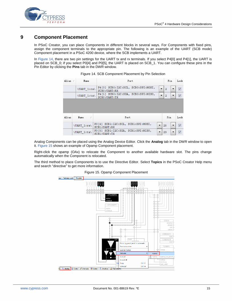
In PSoC Creator, you can place Components in different blocks in several ways. For Components with fixed pins, assign the component terminals to the appropriate pin. The following is an example of the UART (SCB mode) Component placement in a PSoC 4200 device, where the SCB implements a UART.
In Figure 14, there are two pin settings for the UART tx and rx terminals. If you select P4[0] and P4[1], the UART is placed on SCB_0; if you select P0[4] and P0[5], the UART is placed on SCB_1. You can configure these pins in the Pin Editor by clicking the Pins tab in the DWR window.
Figure 14. SCB Component Placement by Pin Selection
Analog Components can be placed using the Analog Device Editor. Click the Analog tab in the DWR window to open
it. Figure 15 shows an example of Opamp Component placement.
Right-click the opamp (OAx) to relocate the Component to another available hardware slot. The pins change automatically when the Component is relocated.
The third method to place Components is to use the Directive Editor. Select Topics in the PSoC Creator Help menu
and search “directive” to get more information.
Figure 15. Opamp Component Placement

PSoC® 4 Hardware Design Considerations
www.cypress.com Document No. 001-88619 Rev. *E 16
10 Analog Module Design Tips
Analog design is always challenging. Using the PSoC 4 analog modules involves several hardware design considerations.
10.1 SAR ADC
PSoC 4 has a 12-bit differential SAR ADC, with a sampling rate up to 1 Msps. As mentioned in I/O Pin Selection, SARMUX [7:0] pins are dedicated for SAR ADC multichannel inputs. They provide the lowest parasitic path
resistance and capacitance. You can also route the signals from other pins to the SAR ADC using the internal analog bus, but doing so will introduce high switch resistance (RSW in Figure 17 on page 17) and additional parasitic capacitance.
PSoC 4 also has an internal precision reference of 1.024 V (±1 percent). You can use other internal references, including VDDA and VDDA / 2, to extend the SAR ADC’s input range. However, note that the accuracy of VDDA and VDDA / 2 as references depends on your power system design, and it probably cannot be better than the 1.024-V precision reference. When you use the internal reference or VDDA / 2 as your reference, a bypass capacitor on VREF pin can help you run the SAR ADC at a faster clock. See Table 2 for details.
Table 2. References for SAR ADC
References Bypass Capacitor
at VREF pin Maximum Component
Clock Frequency
Internal 1.024 V Optional 1.6 MHz
VDDA / 2 Optional 1.6 MHz
VDDA Optional 9 MHz
Internal 1.024 V, bypassed Mandatory 18 MHz
VDDA / 2, bypassed Mandatory 18 MHz
External Vref Mandatory 18 MHz
If you need a reference with a higher accuracy or a specific voltage value, you can connect a custom external reference and a bypass capacitor to the VREF pin.
The SAR ADC is differential physically. When you select single-ended input mode, you must select the connection for the negative input. There are three options: VSS, VREF, and an external pin. The SAR ADC’s input range is affected by the selection as well as by the value of the reference voltage. See the chapter “SAR ADC” in Architecture TRM of PSoC 4 devices for more information.

PSoC® 4 Hardware Design Considerations
www.cypress.com Document No. 001-88619 Rev. *E 17
You can select the reference and the negative input connection in the General tab of the ADC_SAR_SEQ_P4
Component customizer dialog, as Figure 16 shows.
Figure 16. SAR ADC Reference and Negative Input Settings
10.1.1 SAR ADC Acquisi t ion T ime
Another parameter of concern is the SAR ADC acquisition time, which depends on your hardware design, as Figure 17 shows.
Figure 17. Equivalent Sample and Hold Circuit of PSoC 4 SAR ADC
PSoC 4
RSW
Source
RSRC
CHOLDVSRC
Switch
SAR
ADC
VS
S
GN
D
VSRC is the sampled signal source, and RSRC is its output resistance. RSW is the resistance of the path from a dedicated pin to the SAR ADC input, which is about 2.2 kΩ. CHOLD is the sample and hold capacitance, which is about 10 pF.

PSoC® 4 Hardware Design Considerations
www.cypress.com Document No. 001-88619 Rev. *E 18
Figure 18 shows how CHOLD is charged during acquisition time. During acquisition time, the switch in Figure 17 is on. Assuming that CHOLD is charged from 0, acquisition time is the time required to charge CHOLD to a voltage level (VHOLD) such that the error (VSRC – VHOLD) is less than the ADC’s resolution.
Figure 18. CHOLD Charging Process
Voltage
Time
Error < 1/2*LSBVSRC
VHOLD
Acquisition
Time
If the error is smaller than half the ADC’s resolution (1/2 * LSB), it should be okay. The error can be related to the acquisition time in the following equation:
τ
Here, tACQ is the acquisition time, while is the charging time constant.
PSoC 4100/4200 provides a 12-bit differential ADC. If VREF is the reference voltage, the resolution can be expressed in the following equation:
This example assumes that the negative input is connected to VREF, so that VSRC has an input range from 0 to 2 VREF. If the acquisition time is 9 * (RSRC + RSW) * CHOLD, the error can be expressed as follows:

PSoC® 4 Hardware Design Considerations
www.cypress.com Document No. 001-88619 Rev. *E 19
This equation shows that you should choose an acquisition time that is longer than 9 * (RSRC + RSW) * CHOLD to make the error less than 1/2 * LSB of the 12-bit ADC. Select the acquisition time in the Channels tab of the
ADC_SAR_SEQ_P4 Component customizer dialog, as Figure 19 on page 19 shows. Note that when you select the number of ADC clocks, the corresponding acquisition time is automatically calculated. See the ADC_SAR_SEQ_P4 Component datasheet for details.
Figure 19. SAR ADC Acquisition Time Settings
In conclusion, pay attention to the output resistance of the sampled signal source, RSRC, and the resistance introduced by PCB traces in your ADC hardware design. These determine the acquisition time and therefore the sampling rate.

PSoC® 4 Hardware Design Considerations
www.cypress.com Document No. 001-88619 Rev. *E 20
10.2 Opamps
A CTBm block in PSoC 4 provides two opamps, which facilitate your analog signal chain design. You can configure each opamp as an amplifier, a follower, or a comparator, as shown in Figure 20.
You can configure the power mode and output drive capability in the General tab of the OpAmp_P4 customizer
dialog, as Figure 20 shows. The opamps have three power modes. For each power mode, the opamp has a different input offset voltage, gain bandwidth (GBW) product, and operating current. See the device datasheet for specific values.
You should take into account the relation between bandwidth and gain. For example, the highest GBW, 6 MHz, occurs in the high-power/bandwidth mode. In this case, if the bandwidth of the signal to be amplified is 60 kHz, then the gain cannot be higher than 100 or the amplified signal will be distorted.
If you route an opamp output terminal to a pin for external use, select Output to pin for the output mode. If you route the output terminal for internal use, for example to an input of the SAR ADC, select Internal only instead.
Figure 20. OpAmp_P4 Component Settings
10.3 Comparators
PSoC 4 provides as many as six comparators. Four comparators are implemented using the opamps in the CTBm module, and the other two are the low-power comparators. All of the comparators' outputs can be routed to PSoC 4 UDB resources. This helps you leverage the outputs flexibly. For example, you can invert an output’s logic value. PSoC 4 provides three speed modes for each comparator. For each mode, the comparator has a different output slew rate and operating current. See the device datasheet for specific values.
The low-power comparators can monitor external analog voltage levels in low-power modes. For more information, see the device datasheets.
When an analog signal’s voltage is divided by a resistor network before it is input into a comparator, take the input resistance of the comparator into account. You can get the comparator’s input resistance from the device datasheet.

PSoC® 4 Hardware Design Considerations
www.cypress.com Document No. 001-88619 Rev. *E 21
10.4 CapSense
You can connect any PSoC 4 pin to a CapSense sensor except CMOD (or C_MOD) pin, which are reserved for
CMOD. When you need to use a shield electrode for waterproofing or proximity features, you may also need to reserve CTANK (or C_SH_TANK) pin for CSH_TANK. If the parasitic capacitance of the shield is less than 200 pF, it is optional
to use CSH_TANK; otherwise, it is mandatory.
The value for CMOD and CSH_TANK is usually 2.2 nF. The value may be higher if the parasitic capacitance of the sensors is higher.
CapSense detects a finger touch by a tiny variation in the sensor’s capacitance (less than 1 pF). It is very sensitive to both signal and noise. Note the PCB layout tips for CapSense. Refer to PSoC 4 CapSense Design Guide for more details.
Pins with a large sink current that are close to CapSense pins can introduce an offset to the CapSense module’s “GND.” Figure 21 illustrates a switch circuit for CapSense in IDAC source mode. R1 and R2 represent the resistances of PSoC 4 internal traces, and R3 represents the resistance of a PCB trace. A shared return path of sink current and CapSense current is composed of R2 and R3. The closer a pin with a large sink current is to the CapSense pin, the more the sink current that flows through the return path, generating a greater offset.
Figure 21. Sharing Return Path
CS
PSoC 4
Sink Current
VS
S
CapSense Pin
GPIO Pin
R1
R3
R2
CapSense “GND”
AMUXBUS
IDAC
This offset is undesirable and may cause fluctuations in the CapSense reading and possible false triggers. Offset compensation can be done in firmware, but it is strongly recommended that you remove the offset in the hardware design instead. Keep pins with a large sink current as far as possible from the CapSense pins (best practice is by more than three pins). In addition, pay attention to the return path in your PCB. See AN57821 – PSoC 3, PSoC 4, and PSoC 5LP Mixed-Signal Circuit Board Layout Considerations for more details on mixed-signal circuit design.
10.5 Current DACs (IDACs)
PSoC 4 provides up to four IDACs: two 8-bit and the other two 7-bit. See the device datasheet for the electrical specifications. There are two gain options for each IDAC. Table 3 gives the detailed resolutions and capabilities for each IDAC and gain option.
Table 3. IDAC Resolutions and Output Current Capabilities
4X Gain 8X Gain
Step (µA/Bit) Output
Capability (µA) Step (µA/Bit) Output
Capability (µA)
8-Bit IDAC 1.2 306 2.4 612
7-Bit IDAC 1.2 152.4 2.4 304.8

PSoC® 4 Hardware Design Considerations
www.cypress.com Document No. 001-88619 Rev. *E 22
You can set up the IDACs in the Configure tab of the IDAC_P4 Component customizer dialog, as Figure 22 shows.
Figure 22. IDAC Settings
Through two internal analog buses, you can route IDAC outputs to any two different pins that support analog routing.
Note: CapSense requires one or two IDACs. Ensure that the intended IDACs are not used by CapSense.
11 Summary
PSoC 4 provides a flexible solution for designing digital and analog applications. This application note documented the considerations that you need to keep in mind when you build a hardware system around PSoC 4. You can use Appendix B – Family Hardware Resources Look-Up Table to quickly check your hardware design.

PSoC® 4 Hardware Design Considerations
www.cypress.com Document No. 001-88619 Rev. *E 23
12 Related Documents
AN79953 – Getting Started with PSoC 4
AN72845 – Design Guidelines for QFN Packaged Devices
AN86233 – PSoC 4 Low-Power Modes and Power Reduction Techniques
AN80994 – PSoC 3, PSoC 4, and PSoC 5LP EMC Best Practices and Recommendations
AN57821 – PSoC 3, PSoC 4, and PSoC 5LP Mixed-Signal Circuit Board Layout Considerations
AN91445 – Antenna Design Guide
AN91184 – PSoC 4 BLE – Designing BLE Applications
AN95089 – PSoC 4/PRoC BLE Crystal Oscillator Selection and Tuning Techniques
PSoC 4 Application Notes
PSoC 4 CAD Resources
PSoC 4 Device Datasheets
PSoC 4 Technical Reference Manuals
PSoC 4 CapSense Design Guide
Cypress PSoC 4 kit schematics are good examples of how to incorporate PSoC into board schematics. It may be helpful to review the following Cypress kit schematics:
CY8CKIT-040 – PSoC 4000 Pioneer Kit
CY8CKIT-042 – PSoC 4200 Pioneer Kit
CY8CKIT-049 4xxx – PSoC 4100/4200 Prototyping Kit
CY8CKIT-042-BLE - PSoC 4200 BLE Pioneer Kit
CY8CKIT-044 – PSoC 4200M Pioneer Kit
CY8CKIT-043 – PSoC 4200M Prototyping Kit
CY8CKIT-046 – PSoC 4200L Pioneer Kit
Note: On the kit web page, scroll to the link Board Design Files (Schematic, Layout, Gerber, BOM).zip.
About the Author Name: Johnny Zhang
Title: Applications Engineer Sr.
Background: Johnny Zhang graduated from Anhui University with a BSEE and from Tongji University with a MSEE. He is an applications engineer at Cypress and focuses on PSoC applications.

PSoC® 4 Hardware Design Considerations
www.cypress.com Document No. 001-88619 Rev. *E 24
A Appendix A – PCB Layout Tips Note: Before beginning a PCB layout for PSoC, it is a good idea to look at AN57821 – PSoC Mixed-Signal Circuit Board Layout Considerations. Appendix A of that application note shows example PCB layouts and schematics for various PSoC packages.
Note: Cypress PSoC 3, PSoC 4, and PSoC 5LP kit schematics provide good examples of how to incorporate PSoC into board schematics. For more information, see Related Documents.
There are many classic techniques for designing PCBs for low noise and EMC. Some of these techniques include:
Multiple layers: Although they are more expensive, it is best to use a multilayerPCB with separate layers
dedicated to the VSS and VDD supplies. This gives good decoupling and shielding effects. Separate fills on these layers should be provided for VSSA, VSSD, VDDA, VDDIO, and VDDD.
To reduce cost, a two-layer or even a single-layer PCB can be used. In that case, you must have a good layout for all VSS and VDD.
Ground and power supply: There should be a single point for gathering all ground returns. Avoid ground loops,
or minimize their surface area. All component-free surfaces of the PCB should be filled with additional grounding to create a shield, especially when using two-layer or single-layer PCBs.
The power supply should be close to the ground line to minimize the area of the supply loop. The supply loop can act as an antenna and can be a major emitter or receiver of EMI.
Decoupling: The standard decoupler for external power is a 100-µF capacitor. Supplementary 0.1-μF capacitors
should be placed as close as possible to the VSS and VDD pins of the device to reduce high-frequency power supply ripple.
Generally, you should decouple all sensitive or noisy signals to improve the EMC performance. Decoupling can be both capacitive and inductive.
Component position: Separate the circuits on the PCB according to their EMI contribution. This will help reduce
cross-coupling on the PCB. For example, separate noisy high-current circuits, low-voltage circuits, and digital components.
Signal routing: When designing an application, the following areas should be closely studied to improve the
EMC performance:
Noisy signals. For example, signals with fast edge times
Sensitive and high-impedance signals
Signals that capture events, such as interrupts and strobe signals
To improve the EMC performance, keep the trace lengths as short as possible and isolate the traces with VSS traces. To avoid crosstalk, do not route them near to or parallel to other noisy and sensitive traces.
For more information, several references are available:
The Circuit Designer's Companion, Second Edition, (EDN Series for Design Engineers), by Tim Williams
PCB Design for Real-World EMI Control (The Springer International Series in Engineering and Computer Science), by Bruce R. Archambeault and James Drewniak
Printed Circuits Handbook (McGraw Hill Handbooks), by Clyde Coombs
EMC and the Printed Circuit Board: Design, Theory, and Layout Made Simple, by Mark I. Montrose
Signal Integrity Issues and Printed Circuit Board Design, by Douglas Brooks

PSoC® 4 Hardware Design Considerations
www.cypress.com Document No. 001-88619 Rev. *E 25
B Appendix B – Family Hardware Resources Look-Up Table This appendix provides a look-up table, which contains an overview for on-chip hardware resources of different families on PSoC 4 portfolio. The data below show the maximum capability of these families. For detailed information of a specific part, please refer to the corresponding family datasheet.
Features Device Family
CY8C4000 CY8C41000/4200** CY8C4100M/4200M** CY8C4200L
CPU 16-MHz Cortex-M0 48-MHz Cortex-M0 with single-cycle multiply
48-MHz Cortex-M0 with single-cycle multiply
48-MHz Cortex-M0 with single-cycle multiply
DMA N/A N/A 8 channels 32 channels
Flash memory 16 KB 32 KB 128 KB 256 KB
SRAM 2 KB 4 KB 16 KB 32 KB
GPIOs 20 36 55 96
CapSense 16 sensors 35 sensors 54 sensors 94 sensors
ADC None 12-bit, 1-MSPS SAR ADC with sequencer
12-bit, 1-MSPS SAR ADC with sequencer
12-bit, 1-MSPS SAR ADC with sequencer
Opamps None 2 programmable opamps 2 programmable opamps 4 programmable opamps
Comparators 1 CSD comparator with fixed threshold (1.2 V)
2 low-power comparators with wakeup feature
2 low-power comparators with wakeup feature
2 low-power comparators with wakeup feature
IDACs* One 7-bit and one 8-bit One 7-bit and one 8-bit Two 7-bit and two 8-bit Two 7-bit and two 8-bit
Programmable logic blocks (UDBs)
None 4 UDBs, each with eight macrocells and one datapath
4UDBs, each with eight macrocells and one datapath
8UDBs, each with eight macrocells and one datapath
Power supply range 1.71 V to 5.5 V 1.71 V to 5.5 V 1.71 V to 5.5 V 1.71 V to 5.5 V
Low-power modes Deep-sleep at 2.5 µA Deep-sleep at 1.3 µA, Hibernate at 150 nA, Stop at 20 nA
Deep-sleep at 1.3 µA, Hibernate at 150 nA, Stop at 20 nA
Deep-sleep at 1.3 µA, Hibernate at 150 nA, Stop at 20 nA
Segment LCD drive None 4 COM segment LCD drive
4 COM segment LCD drive
8 COM segment LCD drive
Serial communication
One I2C
2 SCBs with programmable I
2C, SPI,
or UART
2 SCBs with programmable I
2C, SPI,
or UART
4 SCBs with programmable I
2C, SPI,
or UART
Timer Counter Pulse-Width Modulator (TCPWM)
1 4 8 8
Controller Area Network (CAN)
None None 2 2
USB None None None Full Speed USB Device with eight endpoints
Clocks
24-MHz / 32-MHz internal main oscillator (IMO)
32-kHz internal low-speed oscillator (ILO)
3-MHz to 48-MHz IMO
32-kHz ILO
3-MHz to 48-MHz IMO
32-kHz ILO
32-kHZ watch crystal oscillator (WCO)
3-MHz to 48-MHz IMO
4-MHz to 33-MHz ECO
32-kHz ILO
32-kHZ watch crystal oscillator (WCO)
Power supply monitoring
Power-on reset (POR),
Brown-out detection (BOD)
POR, BOD, LVD POR, BOD, LVD POR, BOD, LVD
*IDACs are available only when CapSense is not in use. Refer to the respective PSoC 4 Technical Reference Manual for more details.

PSoC® 4 Hardware Design Considerations
www.cypress.com Document No. 001-88619 Rev. *E 26
**PSoC 4100 is only slightly different from PSoC 4200 on CPU frequency, ADC sampling rate, and UDB resources. So is PSoC 4100M from PSoC 4200M. Read Device Datasheets for further details.
Features of PSoC 4-BLE are listed in the table below.
Features
Device Family
CY8C41x7-BLxxx CY8C42x7-BLxxx CY8C41x8-BL CY8C42x8-BL
BLE Subsystem BLE radio and link-layer hardware blocks with Bluetooth 4.1- compatible protocol stack
BLE radio and link-layer hardware blocks with Bluetooth 4.1-compatible protocol stack
BLE radio and link-layer hardware blocks with Bluetooth 4.2- compatible protocol stack**
BLE radio and link-layer hardware blocks with Bluetooth 4.2-compatible protocol stack**
Bluetooth 4.2 Features
LE Secure Connection LE Secure Connection LE Secure Connection, Link Layer Privacy, and Link Layer Data Length Extension**
LE Secure Connection, Link Layer Privacy, and Link Layer Data Length Extension**
CPU 24-MHz ARM® Cortex
®-
M0 CPU with single-cycle multiply
48-MHz ARM Cortex-M0 CPU with single-cycle multiply
24-MHz ARM Cortex-M0 CPU with single-cycle multiply
48-MHz ARM Cortex-M0 CPU with single-cycle multiply
Flash Memory 128 KB 128 KB 256 KB 256 KB
SRAM 16 KB 16 KB 32 KB 32 KB
GPIOs Up to 36 Up to 36 Up to 36 Up to 36
CapSense® Up to 35 sensors Up to 35 sensors Up to 35 sensors Up to 35 sensors
CapSense Gestures
On selected devices On selected devices On selected devices On selected devices
ADC 12-bit, 806-ksps SAR ADC with sequencer
12-bit, 1-Msps SAR ADC with sequencer
12-bit, 806-ksps SAR ADC with sequencer
12-bit, 1-Msps SAR ADC with sequencer
Opamps 2 programmable opamps that are active in deep-sleep mode
4 programmable opamps that are active in deep-sleep mode
2 programmable opamps that are active in deep-sleep mode
4 programmable opamps that are active in deep-sleep mode
Comparators 2 low-power comparators with the wakeup feature
2 low-power comparators with the wakeup feature
2 low-power comparators with the wakeup feature
2 low-power comparators with the wakeup feature
Current DACs One 7-bit, and one 8-bit One 7-bit, and one 8-bit One 7-bit, and one 8-bit One 7-bit, and one 8-bit
Power Supply Range
1.9 V to 5.5 V 1.9 V to 5.5 V 1.9 V to 5.5 V 1.9 V to 5.5 V
Low-Power Modes Deep-sleep mode at 1.3 µA Hibernate mode at 150 nA Stop mode at 60 nA
Deep-sleep mode at 1.3 µA Hibernate mode at 150 nA Stop mode at 60 nA
Deep-sleep mode at 1.3 µA Hibernate mode at 150 nA Stop mode at 60 nA
Deep-sleep mode at 1.3 µA Hibernate mode at 150 nA Stop mode at 60 nA
Segment LCD Drive
4-COM, 32-segment LCD drive on select devices
4-COM, 32-segment LCD drive on select devices
4-COM, 32-segment LCD drive on select devices
4-COM, 32-segment LCD drive on select devices
Serial Communication
2 independent serial communication blocks (SCBs) with programmable I
2C, SPI,
or UART
2 independent SCBs with programmable I
2C,
SPI, or UART
2 independent serial communication blocks (SCBs) with programmable I
2C, SPI,
or UART
2 independent SCBs with programmable I
2C,
SPI, or UART
Timer Counter Pulse-Width Modulator (TCPWM)
4 4 4 4

PSoC® 4 Hardware Design Considerations
www.cypress.com Document No. 001-88619 Rev. *E 27
Features
Device Family
CY8C41x7-BLxxx CY8C42x7-BLxxx CY8C41x8-BL CY8C42x8-BL
Universal Digital Blocks (UDBs)
None 4, each with 8 macrocells and one datapath. Can be used to synthesize additional digital peripherals (Timer, Counter, PWM) or communication interfaces (UART, SPI)
None 4, each with 8 macrocells and one datapath. Can be used to synthesize additional digital peripherals (Timer, Counter, PWM) or communication interfaces (UART, SPI)
Additional Digital Peripherals (I
2S,
PWM)
None Yes (UDB-based digital peripherals on select devices)
None Yes (UDB-based digital peripherals on select devices)
Clocks 3-MHz to 24-MHz IMO
32-kHz ILO
24-MHz ECO
32-kHz WCO
3-MHz to 48-MHz IMO
32-kHz ILO
24-MHz ECO
32-kHz WCO
3-MHz to 24-MHz IMO
32-kHz ILO
24-MHz ECO
32-kHz WCO
3-MHz to 48-MHz IMO
32-kHz ILO
24-MHz ECO
32-kHz WCO
Power Supply Monitoring
Power-on reset (POR) Brown-out detection (BOD) Low-voltage detection (LVD)
POR BOD LVD
POR BOD LVD
POR BOD LVD
Package 56-QFN (7.0 × 7.0 × 0.6 mm) and
68-WLCSP (3.52 × 3.91 × 0.55 mm)
56-QFN (7.0 × 7.0 × 0.6 mm) and
68-WLCSP (3.52 × 3.91 × 0.55 mm)
56-QFN* (7.0 × 7.0 × 0.6 mm) and
76-WLCSP (4.04 × 3.87 × 0.55 mm)
56-QFN* (7.0 × 7.0 × 0.6 mm) and
76-WLCSP (4.04 × 3.87 × 0.55 mm)
DMA None None Up to 8 channels** Up to 8 channels**

PSoC® 4 Hardware Design Considerations
www.cypress.com Document No. 001-88619 Rev. *E 28
C Appendix C – Schematic Checklist The answer to each item in the following checklist should be Yes (Y) or Not Applicable (N.A.). For example, if you power a PSoC 4 device with an unregulated external supply in your application, you can mark all the items of “Power (regulated external supply)” as N.A.
Catalog Item Y/N/N.A. Remark
Power Is the voltage at the VDDA pin always greater than or equal to the voltages at the VDDD pins?
Is VDDIO ≤ VDDD ≤ VDDA?
Power (unregulated external supply)
Are the power supply pin connections made in accordance with Figure 4?
Are the 0.1-μF and 1-μF capacitors connected to each VDDD, VDDIO, VDDA, or VDDR pin?
Are the voltages (including ripples) at the VDDD and VDDA pins in the range of 1.8 V to 5.5 V?
Is the VCCD pin connected to a 1-μF capacitor and no other external load?
Is the VCCD pin unconnected with an external supply?
Is the power supply on the VDDR pin higher than 1.9 V.
Power (regulated external supply)
Are the power supply pin connections made in accordance with Figure 5?
Are the 0.1-μF and 1-μF ceramic decoupling capacitors connected to each VCCD, VDDD, and VDDA pin?
Are the voltages (including ripples) at the VDDD and VDDA pins in the range of 1.71 V to 1.89 V?
Does your PSoC device belong to non-BLE families?
Clocking Is the external clock connected to EXT_CLK pin?
Is the external clock’s frequency less than or equal to 48 MHz (including tolerance)?
Is the external clock’s duty cycle from 45 percent to 55 percent?
Reset Is the reset pin connection made in accordance with Figure 9?
Programming and debugging
Is the SWD connector’s pin map in accordance with one of the pin maps in Figure 11?
Are the SWD signals connected to SWD_CLK pin and SWD_DATA pin?
GPIO pins Is the assignment of your GPIO pins done in the sequence described in I/O Pin Selection?
Is any GPIO pin’s sink current lower than 8 mA?
Is any GPIO pin’s source current lower than 4 mA?
Is the GPIO pins’ total source current or sink current smaller than device capability?
Are Port 4,5,6,7 pins used according to Port 4, 5, 6, and 7 GPIO Pins?
Low-power comparators
Is the assignment of the low-power comparators’ fixed pins in accordance with Table 2?
CTBm Is the assignment of the CTBm’s fixed pins in accordance with Table 3?
SCB Is the assignment of the SCB’s fixed pins in accordance with the device datasheet?
SAR ADC Is the connection of the P1[7] bypass capacitor in accordance with Table 2?
Is the acquisition time of each SAR ADC channel enough to keep the error less than 1/2 LSB?
CapSense Are the pins with strong sink current kept away from the CapSense pins (the space is more than three pins)?
Is CMOD connected to CMOD (or C_MOD) pin?
Is CSH_TANK connected to CTANK (or C_SH_TANK) pin?
IDAC Is the IDAC not being used by CapSense?

PSoC® 4 Hardware Design Considerations
www.cypress.com Document No. 001-88619 Rev. *E 29
Document History
Document Title: AN88619 - PSoC® 4 Hardware Design Considerations
Document Number: 001-88619
Revision ECN Orig. of Change
Submission Date
Description of Change
** 4293447 JOZH 02/27/2014 New application note
*A 4517949 JOZH 10/07/2014 Changed the title to “PSoC® 4100/4200 Hardware Design Considerations -
AN88619” to address only PSoC 4100/4200 devices
Corrected names and links for reference documents
Added the latest references
Added the link for PSoC 4100/4200 SCH and PCB libraries
*B 4701455 JOZH 03/25/2015 Added a table to illustrate the differences between PSoC 4100 and PSoC 4200
Added TQFP-48 descriptions
Added variable VDDA introduction
Added routed clock introduction in "Clocking" section
Updated PSoC Creator Component snapshot per PSoC Creator 3.1
*C 4772693 NIDH 05/26/2015 Updated for PSoC 4100M/4200M device
Updated template
Changed the title
*D 4965182 JOZH 10/15/2015 Updated the descriptions to accommodate all PSoC 4 device families
Corrected SAR’s clock frequency upper limits under different VREF pin connection scenarios
Refreshed the snapshots with PSoC Creator 3.2
Corrected the VCCD pin capacitor value from 0.1 μF to 1 μF
Clarified that HFCLK connection to pin is not available
*E 5054801 NIDH/JOZH 01/29/2016 Added self-help section in the beginning of the document.
Added PSoC 4 L-series information throughout the document.
Updated Power Supply Diagram for PSoC 4 BLE.
Updated Checklist for PSoC 4 BLE and the VCCD pin usage.
Added Cross References to BLE Documents.

PSoC® 4 Hardware Design Considerations
www.cypress.com Document No. 001-88619 Rev. *E 30
Worldwide Sales and Design Support
Cypress maintains a worldwide network of offices, solution centers, manufacturer’s representatives, and distributors. To find the office closest to you, visit us at Cypress Locations.
Products
Automotive cypress.com/go/automotive
Clocks & Buffers cypress.com/go/clocks
Interface cypress.com/go/interface
Lighting & Power Control cypress.com/go/powerpsoc
Memory cypress.com/go/memory
PSoC cypress.com/go/psoc
Touch Sensing cypress.com/go/touch
USB Controllers cypress.com/go/usb
Wireless/RF cypress.com/go/wireless
PSoC® Solutions
psoc.cypress.com/solutions
PSoC 1 | PSoC 3 | PSoC 4 | PSoC 5LP
Cypress Developer Community
Community | Forums | Blogs | Video | Training
Technical Support
cypress.com/go/support
PSoC is a registered trademark and PSoC Creator is a trademark of Cypress Semiconductor Corp. All other trademarks or registered trademarks referenced herein are the property of their respective owners.
Cypress Semiconductor 198 Champion Court San Jose, CA 95134-1709
Phone : 408-943-2600 Fax : 408-943-4730 Website : www.cypress.com
© Cypress Semiconductor Corporation, 2014-2016. The information contained herein is subject to change without notice. Cypress Semiconductor Corporation assumes no responsibility for the use of any circuitry other than circuitry embodied in a Cypress product. Nor does it convey or imply any license under patent or other rights. Cypress products are not warranted nor intended to be used for medical, life support, life saving, critical control or safety applications, unless pursuant to an express written agreement with Cypress. Furthermore, Cypress does not authorize its products for use as critical components in life-support systems where a malfunction or failure may reasonably be expected to result in significant injury to the user. The inclusion of Cypress products in life-support systems application implies that the manufacturer assumes all risk of such use and in doing so indemnifies Cypress against all charges. This Source Code (software and/or firmware) is owned by Cypress Semiconductor Corporation (Cypress) and is protected by and subject to worldwide patent protection (United States and foreign), United States copyright laws and international treaty provisions. Cypress hereby grants to licensee a personal, non-exclusive, non-transferable license to copy, use, modify, create derivative works of, and compile the Cypress Source Code and derivative works for the sole purpose of creating custom software and or firmware in support of licensee product to be used only in conjunction with a Cypress integrated circuit as specified in the applicable agreement. Any reproduction, modification, translation, compilation, or representation of this Source Code except as specified above is prohibited without the express written permission of Cypress. Disclaimer: CYPRESS MAKES NO WARRANTY OF ANY KIND, EXPRESS OR IMPLIED, WITH REGARD TO THIS MATERIAL, INCLUDING, BUT NOT LIMITED TO, THE IMPLIED WARRANTIES OF MERCHANTABILITY AND FITNESS FOR A PARTICULAR PURPOSE. Cypress reserves the right to make changes without further notice to the materials described herein. Cypress does not assume any liability arising out of the application or use of any product or circuit described herein. Cypress does not authorize its products for use as critical components in life-support systems where a malfunction or failure may reasonably be expected to result in significant injury to the user. The inclusion of Cypress’ product in a life-support systems application implies that the manufacturer assumes all risk of such use and in doing so indemnifies Cypress against all charges. Use may be limited by and subject to the applicable Cypress software license agreement.