Embed Size (px)
Citation preview
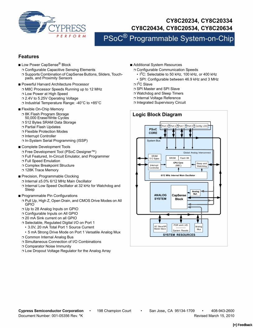
CY8C20234, CY8C20334CY8C20434, CY8C20534, CY8C20634
PSoC® Programmable System-on-Chip
Cypress Semiconductor Corporation • 198 Champion Court • San Jose, CA 95134-1709 • 408-943-2600Document Number: 001-05356 Rev. *K Revised March 15, 2010
Features■ Low Power CapSense® Block
❐ Configurable Capacitive Sensing Elements❐ Supports Combination of CapSense Buttons, Sliders, Touch-
pads, and Proximity Sensors
■ Powerful Harvard Architecture Processor❐ M8C Processor Speeds Running up to 12 MHz❐ Low Power at High Speed❐ 2.4V to 5.25V Operating Voltage❐ Industrial Temperature Range: -40°C to +85°C
■ Flexible On-Chip Memory❐ 8K Flash Program Storage
50,000 Erase/Write Cycles ❐ 512 Bytes SRAM Data Storage❐ Partial Flash Updates❐ Flexible Protection Modes❐ Interrupt Controller❐ In-System Serial Programming (ISSP)
■ Complete Development Tools❐ Free Development Tool (PSoC Designer™)❐ Full Featured, In-Circuit Emulator, and Programmer❐ Full Speed Emulation❐ Complex Breakpoint Structure❐ 128K Trace Memory
■ Precision, Programmable Clocking❐ Internal ±5.0% 6/12 MHz Main Oscillator❐ Internal Low Speed Oscillator at 32 kHz for Watchdog and
Sleep
■ Programmable Pin Configurations❐ Pull Up, High Z, Open Drain, and CMOS Drive Modes on All
GPIO❐ Up to 28 Analog Inputs on GPIO❐ Configurable Inputs on All GPIO❐ 20 mA Sink current on all GPIO❐ Selectable, Regulated Digital I/O on Port 1
• 3.0V, 20 mA Total Port 1 Source Current• 5 mA Strong Drive Mode on Port 1 Versatile Analog Mux
❐ Common Internal Analog Bus❐ Simultaneous Connection of I/O Combinations ❐ Comparator Noise Immunity❐ Low Dropout Voltage Regulator for the Analog Array
■ Additional System Resources❐ Configurable Communication Speeds
• I2C: Selectable to 50 kHz, 100 kHz, or 400 kHz• SPI: Configurable between 46.9 kHz and 3 MHz
❐ I2C Slave ❐ SPI Master and SPI Slave❐ Watchdog and Sleep Timers❐ Internal Voltage Reference❐ Integrated Supervisory Circuit
SRAM512 Bytes
System Bus
InterruptController
6/12 MHz Internal Main Oscillator
Global Analog Interconnect
PSoCCORE
CPU Core(M8C)
SROM Flash 8K
SYSTEM RESOURCES
ANALOGSYSTEM
AnalogRef.
I2C Slave/SPIMaster-Slave
POR and LVD
System Resets
Port 1 Port 0
Sleep andWatchdog
AnalogMux
Port 3 Port 2
CapSenseBlock
Config LDO
Logic Block Diagram
[+] Feedback [+] Feedback [+] Feedback
CY8C20234, CY8C20334CY8C20434, CY8C20534, CY8C20634
Document Number: 001-05356 Rev. *K Page 2 of 37
ContentsFeatures............................................................................. 1Logic Block Diagram........................................................ 1Contents ............................................................................ 2PSoC® Functional Overview ........................................... 3
PSoC Core .................................................................. 3CapSense Analog System .......................................... 3Additional System Resources ..................................... 4
Getting Started.................................................................. 4Application Notes ........................................................ 4Development Kits ........................................................ 4Training ....................................................................... 4Cypros Consultants ..................................................... 4Solutions Library.......................................................... 4Technical Support ....................................................... 4
Development Tools .......................................................... 5PSoC Designer Software Subsystems........................ 5In-Circuit Emulator....................................................... 5
Designing with PSoC Designer ....................................... 6Select Components ..................................................... 6Configure Components ............................................... 6Organize and Connect ................................................ 6Generate, Verify, and Debug....................................... 6
Document Conventions ................................................... 7Units of Measure ......................................................... 7Numeric Naming.......................................................... 7
Pin Information ................................................................. 848-Pin OCD Part Pinout ............................................... 8
16-Pin Part Pinout ..................................................... 1024-Pin Part Pinout ..................................................... 1132-Pin Part Pinout ..................................................... 1228-Pin Part Pinout ..................................................... 1430-Ball Part Pinout .................................................... 15
Electrical Specifications ................................................ 16Absolute Maximum Ratings .......................................... 17Operating Temperature.................................................. 17DC Electrical Characteristics ........................................ 18
DC General Purpose I/O Specifications .................... 18AC Electrical Characteristics ........................................ 22Packaging Dimensions .................................................. 29
Thermal Impedances................................................. 32Solder Reflow Peak Temperature ............................. 32
Development Tool Selection ......................................... 33Software .................................................................... 33Development Kits ...................................................... 33
Evaluation Tools............................................................. 33Device Programmers................................................. 34Accessories (Emulation and Programming) .............. 34
Ordering Information...................................................... 35Document History Page................................................. 36Sales, Solutions, and Legal Information ...................... 37
Worldwide Sales and Design Support....................... 37Products .................................................................... 37PSoC Solutions ......................................................... 37
[+] Feedback [+] Feedback [+] Feedback
CY8C20234, CY8C20334CY8C20434, CY8C20534, CY8C20634
Document Number: 001-05356 Rev. *K Page 3 of 37
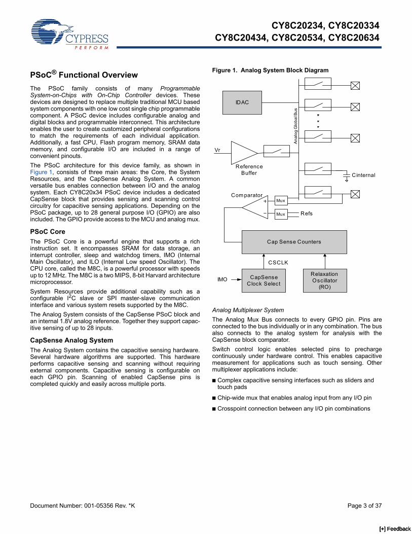
PSoC® Functional OverviewThe PSoC family consists of many Programmable System-on-Chips with On-Chip Controller devices. These devices are designed to replace multiple traditional MCU based system components with one low cost single chip programmable component. A PSoC device includes configurable analog and digital blocks and programmable interconnect. This architecture enables the user to create customized peripheral configurations to match the requirements of each individual application. Additionally, a fast CPU, Flash program memory, SRAM data memory, and configurable I/O are included in a range of convenient pinouts.The PSoC architecture for this device family, as shown in Figure 1, consists of three main areas: the Core, the System Resources, and the CapSense Analog System. A common versatile bus enables connection between I/O and the analog system. Each CY8C20x34 PSoC device includes a dedicated CapSense block that provides sensing and scanning control circuitry for capacitive sensing applications. Depending on the PSoC package, up to 28 general purpose I/O (GPIO) are also included. The GPIO provide access to the MCU and analog mux.
PSoC CoreThe PSoC Core is a powerful engine that supports a rich instruction set. It encompasses SRAM for data storage, an interrupt controller, sleep and watchdog timers, IMO (Internal Main Oscillator), and ILO (Internal Low speed Oscillator). The CPU core, called the M8C, is a powerful processor with speeds up to 12 MHz. The M8C is a two MIPS, 8-bit Harvard architecture microprocessor.System Resources provide additional capability such as a configurable I2C slave or SPI master-slave communication interface and various system resets supported by the M8C.The Analog System consists of the CapSense PSoC block and an internal 1.8V analog reference. Together they support capac-itive sensing of up to 28 inputs.
CapSense Analog SystemThe Analog System contains the capacitive sensing hardware. Several hardware algorithms are supported. This hardware performs capacitive sensing and scanning without requiring external components. Capacitive sensing is configurable on each GPIO pin. Scanning of enabled CapSense pins is completed quickly and easily across multiple ports.
Figure 1. Analog System Block Diagram
Analog Multiplexer SystemThe Analog Mux Bus connects to every GPIO pin. Pins are connected to the bus individually or in any combination. The bus also connects to the analog system for analysis with the CapSense block comparator.Switch control logic enables selected pins to precharge continuously under hardware control. This enables capacitive measurement for applications such as touch sensing. Other multiplexer applications include:
■ Complex capacitive sensing interfaces such as sliders and touch pads
■ Chip-wide mux that enables analog input from any I/O pin
■ Crosspoint connection between any I/O pin combinations
IDAC
ReferenceBuffer
Vr
Cinternal
Ana
log
Glo
bal B
us
Cap Sense Counters
Com paratorMux
Mux Refs
CapSenseClock Select
RelaxationOscillator
(RO)
CSCLK
IMO
[+] Feedback [+] Feedback [+] Feedback
CY8C20234, CY8C20334CY8C20434, CY8C20534, CY8C20634
Document Number: 001-05356 Rev. *K Page 4 of 37
Additional System ResourcesSystem Resources provide additional capability useful to complete systems. Additional resources include low voltage detection and power on reset. Brief statements describing the merits of each system resource follow:
■ The I2C slave or SPI master-slave module provides 50/100/400 kHz communication over two wires. SPI communication over three or four wires run at speeds of 46.9 kHz to 3 MHz (lower for a slower system clock).
■ Low Voltage Detection (LVD) interrupts signal the application of falling voltage levels, while the advanced POR (Power On Reset) circuit eliminates the need for a system supervisor.
■ An internal 1.8V reference provides an absolute reference for capacitive sensing.
■ The 5V maximum input, 3V fixed output, low dropout regulator (LDO) provides regulation for I/Os. A register controlled bypass mode enables the user to disable the LDO.
Getting StartedThe quickest way to understand PSoC silicon is to read this data sheet and then use the PSoC Designer Integrated Development Environment (IDE). This data sheet is an overview of the PSoC integrated circuit and presents specific pin, register, and electrical specifications. For in depth information, along with detailed programming infor-mation, see the Technical Reference Manual for this PSoC device.For up-to-date ordering, packaging, and electrical specification information, see the latest PSoC device data sheets on the web at http://www.cypress.com.
Application NotesApplication notes are an excellent introduction to the wide variety of possible PSoC designs and are available at http://www.cypress.com.
Development KitsPSoC Development Kits are available online from Cypress at http://www.cypress.com and through a growing number of regional and global distributors, which include Arrow, Avnet, Digi-Key, Farnell, Future Electronics, and Newark.
TrainingFree PSoC technical training (on demand, webinars, and workshops) is available online at http://www.cypress.com. The training covers a wide variety of topics and skill levels to assist you in your designs.
Cypros ConsultantsCertified PSoC Consultants offer everything from technical assistance to completed PSoC designs. To contact or become a PSoC Consultant, go to http://www.cypress.com and refer to CYPros Consultants.
Solutions LibraryVisit our growing library of solution focused designs at http://www.cypress.com. Here you can find various application designs that include firmware and hardware design files that enable you to complete your designs quickly.
Technical Support
For assistance with technical issues, search KnowledgeBase articles and forums at http://www.cypress.com. If you cannot find an answer to your question, call technical support at 1-800-541-4736.
[+] Feedback [+] Feedback [+] Feedback
CY8C20234, CY8C20334CY8C20434, CY8C20534, CY8C20634
Document Number: 001-05356 Rev. *K Page 5 of 37
Development ToolsPSoC Designer is a Microsoft® Windows-based, integrated development environment for the Programmable System-on-Chip (PSoC) devices. The PSoC Designer IDE runs on Windows XP or Windows Vista. This system provides design database management by project, an integrated debugger with In-Circuit Emulator, in-system programming support, and built-in support for third-party assemblers and C compilers. PSoC Designer also supports C language compilers developed specifically for the devices in the PSoC family.
PSoC Designer Software Subsystems
System-Level ViewA drag-and-drop visual embedded system design environment based on PSoC Express. In the system level view you create a model of your system inputs, outputs, and communication inter-faces. You define when and how an output device changes state based upon any or all other system devices. Based upon the design, PSoC Designer automatically selects one or more PSoC Mixed-Signal Controllers that match your system requirements.PSoC Designer generates all embedded code, then compiles and links it into a programming file for a specific PSoC device.
Chip-Level ViewThe chip-level view is a more traditional integrated development environment (IDE). Choose a base device to work with and then select different onboard analog and digital components called user modules that use the PSoC blocks. Examples of user modules are ADCs, DACs, Amplifiers, and Filters. Configure the user modules for your chosen application and connect them to each other and to the proper pins. Then generate your project. This prepopulates your project with APIs and libraries that you can use to program your application.The device editor also supports easy development of multiple configurations and dynamic reconfiguration. Dynamic configuration enables changing configurations at run time.
Hybrid DesignsYou can begin in the system-level view, allow it to choose and configure your user modules, routing, and generate code, then switch to the chip-level view to gain complete control over on-chip resources. All views of the project share a common code editor, builder, and common debug, emulation, and programming tools.
Code Generation ToolsPSoC Designer supports multiple third party C compilers and assemblers. The code generation tools work seamlessly within the PSoC Designer interface and have been tested with a full range of debugging tools. The choice is yours.
Assemblers. The assemblers enable assembly code to merge seamlessly with C code. Link libraries automatically use absolute addressing or are compiled in relative mode, and linked with other software modules to get absolute addressing.
C Language Compilers. C language compilers are available that support the PSoC family of devices. The products enable you to create complete C programs for the PSoC family devices.The optimizing C compilers provide all the features of C tailored to the PSoC architecture. They come complete with embedded libraries providing port and bus operations, standard keypad and display support, and extended math functionality.
DebuggerThe PSoC Designer Debugger subsystem provides hardware in-circuit emulation, allowing you to test the program in a physical system while providing an internal view of the PSoC device. Debugger commands enable the designer to read and program and read and write data memory, read and write I/O registers, read and write CPU registers, set and clear breakpoints, and provide program run, halt, and step control. The debugger also enables the designer to create a trace buffer of registers and memory locations of interest.
Online Help SystemThe online help system displays online, context-sensitive help for the user. Designed for procedural and quick reference, each functional subsystem has its own context-sensitive help. This system also provides tutorials and links to FAQs and an Online Support Forum to aid the designer in getting started.
In-Circuit EmulatorA low cost, high functionality In-Circuit Emulator (ICE) is available for development support. This hardware has the capability to program single devices.The emulator consists of a base unit that connects to the PC by way of a USB port. The base unit is universal and operates with all PSoC devices. Emulation pods for each device family are available separately. The emulation pod takes the place of the PSoC device in the target board and performs full speed (24 MHz) operation.
[+] Feedback [+] Feedback [+] Feedback
CY8C20234, CY8C20334CY8C20434, CY8C20534, CY8C20634
Document Number: 001-05356 Rev. *K Page 6 of 37
Designing with PSoC DesignerThe development process for the PSoC device differs from that of a traditional fixed function microprocessor. The configurable analog and digital hardware blocks give the PSoC architecture a unique flexibility that pays dividends in managing specification change during development and by lowering inventory costs. These configurable resources, called PSoC Blocks, have the ability to implement a wide variety of user-selectable functions. The PSoC development process can be summarized in the following four steps: 1. Select components2. Configure components3. Organize and Connect4. Generate, Verify, and Debug
Select ComponentsBoth the system-level and chip-level views provide a library of prebuilt, pretested hardware peripheral components. In the system-level view, these components are called “drivers” and correspond to inputs (a thermistor, for example), outputs (a brushless DC fan, for example), communication interfaces (I2C-bus, for example), and the logic to control how they interact with one another (called valuators). In the chip-level view, the components are called “user modules”. User modules make selecting and implementing peripheral devices simple, and come in analog, digital, and mixed signal varieties.
Configure ComponentsEach of the components you select establishes the basic register settings that implement the selected function. They also provide parameters and properties that enable you to tailor their precise configuration to your particular application. For example, a Pulse Width Modulator (PWM) User Module configures one or more digital PSoC blocks, one for each 8 bits of resolution. The user module parameters permit you to establish the pulse width and duty cycle. Configure the parameters and properties to correspond to your chosen application. Enter values directly or by selecting values from drop-down menus.Both the system-level drivers and chip-level user modules are documented in data sheets that are viewed directly in PSoC Designer. These data sheets explain the internal operation of the component and provide performance specifications. Each data sheet describes the use of each user module parameter or driver property, and other information you may need to successfully implement your design.
Organize and ConnectYou can build signal chains at the chip level by interconnecting user modules to each other and the I/O pins, or connect system level inputs, outputs, and communication interfaces to each other with valuator functions.In the system-level view, selecting a potentiometer driver to control a variable speed fan driver and setting up the valuators to control the fan speed based on input from the pot selects, places, routes, and configures a programmable gain amplifier (PGA) to buffer the input from the potentiometer, an analog to digital converter (ADC) to convert the potentiometer’s output to a digital signal, and a PWM to control the fan. In the chip-level view, perform the selection, configuration, and routing so that you have complete control over the use of all on-chip resources.
Generate, Verify, and DebugWhen you are ready to test the hardware configuration or move on to developing code for the project, perform the “Generate Application” step. This causes PSoC Designer to generate source code that automatically configures the device to your specification and provides the software for the system.Both system-level and chip-level designs generate software based on your design. The chip-level design provides application programming interfaces (APIs) with high level functions to control and respond to hardware events at run-time and interrupt service routines that you can adapt as needed. The system-level design also generates a C main() program that completely controls the chosen application and contains placeholders for custom code at strategic positions allowing you to further refine the software without disrupting the generated code.A complete code development environment allows you to develop and customize your applications in C, assembly language, or both.The last step in the development process takes place inside PSoC Designer’s Debugger subsystem. The Debugger downloads the HEX image to the ICE where it runs at full speed. Debugger capabilities rival those of systems costing many times more. In addition to traditional single-step, run-to-breakpoint and watch-variable features, the Debugger provides a large trace buffer and allows you define complex breakpoint events that include monitoring address and data bus values, memory locations and external signals.
[+] Feedback [+] Feedback [+] Feedback
CY8C20234, CY8C20334CY8C20434, CY8C20534, CY8C20634
Document Number: 001-05356 Rev. *K Page 7 of 37
Document ConventionsTable 1 lists the acronyms that are used in this document.
Units of MeasureA units of measure table is located in the Electrical Specifications section. Table 8 on page 16 lists all the abbreviations used to measure the PSoC devices.
Numeric NamingHexadecimal numbers are represented with all letters in uppercase with an appended lowercase ‘h’ (for example, ‘14h’ or ‘3Ah’). Hexadecimal numbers are also represented by a ‘0x’ prefix, the C coding convention. Binary numbers have an appended lowercase ‘b’ (for example, 01010100b or 01000011b). Numbers not indicated by an ‘h’, ‘b’, or 0x are decimals.
Table 1. Acronyms Used
Acronym DescriptionAC Alternating CurrentAPI Application Programming InterfaceCPU Central Processing UnitDC Direct CurrentGPIO General Purpose I/OGUI Graphical User InterfaceICE In-Circuit EmulatorILO Internal Low Speed OscillatorIMO Internal Main OscillatorI/O Input Or OutputLSb Least Significant BitLVD Low Voltage DetectMSb Most Significant BitPOR Power On ResetPPOR Precision Power On ResetPSoC® Programmable System-on-ChipSLIMO Slow IMOSRAM Static Random Access Memory
[+] Feedback [+] Feedback [+] Feedback
CY8C20234, CY8C20334CY8C20434, CY8C20534, CY8C20634
Document Number: 001-05356 Rev. *K Page 8 of 37
Pin Information This section describes, lists, and illustrates the CY8C20234, CY8C20334, CY8C20434, CY8C20534, and CY8C20634 PSoC device pins and pinout configurations.The CY8C20x34 PSoC device is available in a variety of packages that are listed and shown in the following tables. Every port pin (labeled with a “P”) is capable of Digital I/O and connection to the common analog bus. However, Vss, Vdd, and XRES are not capable of Digital I/O.
48-Pin OCD Part PinoutThe 48-Pin QFN part table and pin diagram is for the CY8C20000 On-Chip Debug (OCD) PSoC device. This part is only used for in-circuit debugging. It is NOT available for production.
Figure 2. CY8C20000 48-Pin OCD PSoC Device
OCD QFN
NC
Vss
P0[3
], AI
P0[5
], AI
P0[7
], AI
OC
DE
OC
DO
Vdd
P0[6
], AI
NC
NC
NC
101112
NCAI, P0[1]AI, P2[7]AI, P2[5]AI, P2[3]AI, P2[1]AI, P3[3]AI, P3[1]
AI, I2C SCL, SPI SS, P1[7]AI, I2C SDA, SPI MISO, P1[5]
NCNC
3534333231302928272625
3648 47 46 45 44 43 42 41 40 39 38 37
P0[2], AIP0[0], AIP2[6], AIP2[4], AIP2[2], AIP2[0], AIP3[2], AIP3[0], AIXRESP1[6], AIP1[4], EXTCLK, AI
P0[4], AI123456789
13 14 15 16 17 18 19 20 21 22 23 24
NC
NC
AI, S
PI C
LK, P
1[3]
AI, C
LK*,
I2C
SC
L, S
PI M
OS
I, P1
[1]
Vss
CC
LKH
CLK
AI,
DAT
A*, I
2C S
DA,
P1[
0]A
I, P1
[2]
NC
NC
NC
Table 2. Pin Definitions - CY8C20000 48-Pin OCD (QFN) [2]
Pin No. Digital Analog Name Description1 NC No Connection2 I/O I P0[1]3 I/O I P2[7]4 I/O I P2[5]5 I/O I P2[3]6 I/O I P2[1]7 I/O I P3[3]8 I/O I P3[1]9 IOH I P1[7] I2C SCL, SPI SS10 IOH I P1[5] I2C SDA, SPI MISO11 I/O I P0[1]12 NC No Connection13 NC No Connection14 NC No Connection
[+] Feedback [+] Feedback [+] Feedback
CY8C20234, CY8C20334CY8C20434, CY8C20534, CY8C20634
Document Number: 001-05356 Rev. *K Page 9 of 37
15 NC SPI CLK16 IOH I P1[3] CLK[1], I2C SCL, SPI MOSI17 IOH I P1[1] Ground Connection18 Power Vss OCD CPU Clock Output19 CCLK OCD High Speed Clock Output20 HCLK DATA[1], I2C SDA21 IOH I P1[0]
22 IOH I P1[2] No Connection23 NC No Connection24 NC No Connection25 NC Optional External Clock Input (EXTCLK)26 IOH I P1[4]27 IOH I P1[6] Active High External Reset with Internal Pull Down28 Input XRES29 I/O I P3[0]30 I/O I P3[2]31 I/O I P2[0]32 I/O I P2[2]33 I/O I P2[4]34 I/O I P2[6]35 I/O I P0[0]36 I/O I P0[2]37 NC No Connection38 NC No Connection39 NC No Connection40 I/O I P0[6] Analog Bypass41 Power Vdd Supply Voltage42 OCDO OCD Odd Data Output43 OCDE OCD Even Data I/O44 I/O I P0[7]45 I/O I P0[5]46 I/O I P0[3] Integrating Input47 Power Vss Ground Connection48 NC No ConnectionCP Power Vss Center Pad is connected to GroundA = Analog, I = Input, O = Output, NC = No Connection H = 5 mA High Output Drive.
Table 2. Pin Definitions - CY8C20000 48-Pin OCD (QFN) [2] (continued)
Pin No. Digital Analog Name Description
[+] Feedback [+] Feedback [+] Feedback

CY8C20234, CY8C20334CY8C20434, CY8C20534, CY8C20634
Document Number: 001-05356 Rev. *K Page 10 of 37
16-Pin Part Pinout Figure 3. CY8C20234 16-Pin PSoC Device
Table 3. Pin Definitions - CY8C20234 16-Pin (QFN no e-pad)
Pin No.Type
Name DescriptionDigital Analog
1 I/O I P2[5]2 I/O I P2[1]3 IOH I P1[7] I2C SCL, SPI SS4 IOH I P1[5] I2C SDA, SPI MISO5 IOH I P1[3] SPI CLK6 IOH I P1[1] CLK[1], I2C SCL, SPI MOSI7 Power Vss Ground Connection8 IOH I P1[0] DATA[1], I2C SDA9 IOH I P1[2]10 IOH I P1[4] Optional External Clock Input (EXTCLK)11 Input XRES Active High External Reset with Internal Pull Down12 I/O I P0[4]13 Power Vdd Supply Voltage14 I/O I P0[7]15 I/O I P0[3] Integrating Input16 I/O I P0[1]A = Analog, I = Input, O = Output, OH = 5 mA High Output Drive
QFN(Top View)
AI, P2[5]
AI, I2C SCL, SPI SS, P1[7]AI, I2C SDA, SPI MISO, P1[5]
AI,
SP
I CLK
, P1[
3]
1234
1110
9
16 15 14 13
P0[3
], AI
P0[7
], AI
Vdd
P0[4], AI
CLK
, I2C
SC
L, S
PI M
OSI
P1[
1]
AI, D
ATA
, I2C
SD
A, P
1[0]
P1[2], AI
AI, P2[1]P1[4], AI, EXTCLKXRES
P0[1
], AI
Vss
12
5 6 7 8
Note1. These are the ISSP pins, that are not High Z at POR (Power On Reset). See the PSoC Programmable System-on-Chip Technical Reference Manual for details.
[+] Feedback [+] Feedback [+] Feedback

CY8C20234, CY8C20334CY8C20434, CY8C20534, CY8C20634
Document Number: 001-05356 Rev. *K Page 11 of 37
24-Pin Part PinoutFigure 4. CY8C20334 24-Pin PSoC Device
QFN(Top View)
AI, P2[5]
AI, I2C SCL, SPI SS, P1[7]AI, I2C SDA, SPI MISO, P1[5]
AI, SPI CLK, P1[3]
123456
181716151413
P0[2], AIP0[0], AI
24 23 22 21 20 19
P0[
3], A
IP
0[5]
, AI
P0[
7], A
IV
dd
P0[4], AI
7 8 9 10 11 12
SP
I MO
SI,
P1[
1]
AI,
DA
TA*,
I2C
SD
A, P
1[0]
AI,
P1[
2]
AI, P2[3]AI, P2[1]
NC
P1[6], AI
AI,
EX
TCLK
, P1[
4]
XRESP2[0], AI
P0[
6], A
I
AI, C
LK*,
I2C
SC
LP
0[1]
, AI
Vss
Table 4. Pin Definitions - CY8C20334 24-Pin (QFN) [2]
Pin No.Type
Name DescriptionDigital Analog
1 I/O I P2[5]2 I/O I P2[3]3 I/O I P2[1]4 IOH I P1[7] I2C SCL, SPI SS5 IOH I P1[5] I2C SDA, SPI MISO6 IOH I P1[3] SPI CLK7 IOH I P1[1] CLK[1], I2C SCL, SPI MOSI8 NC No Connection9 Power Vss Ground Connection10 IOH I P1[0] DATA[1], I2C SDA11 IOH I P1[2]12 IOH I P1[4] Optional External Clock Input (EXTCLK)13 IOH I P1[6]14 Input XRES Active High External Reset with Internal Pull Down15 I/O I P2[0]16 I/O I P0[0]17 I/O I P0[2]18 I/O I P0[4]19 I/O I P0[6] Analog Bypass20 Power Vdd Supply Voltage21 I/O I P0[7]22 I/O I P0[5]23 I/O I P0[3] Integrating Input24 I/O I P0[1]CP Power Vss Center Pad is connected to GroundA = Analog, I = Input, O = Output, OH = 5 mA High Output Drive
Note2. The center pad on the QFN package is connected to ground (Vss) for best mechanical, thermal, and electrical performance. If not connected to ground, it is electrically
floated and not connected to any other signal.
[+] Feedback [+] Feedback [+] Feedback

CY8C20234, CY8C20334CY8C20434, CY8C20534, CY8C20634
Document Number: 001-05356 Rev. *K Page 12 of 37
32-Pin Part PinoutFigure 5. CY8C20434 32-Pin PSoC Device
AI, P0[1]AI, P2[7]AI, P2[5]AI, P2[3]AI, P2[1]AI, P3[3]
QFN(Top View)
9 10 11 12 13 14 15 16
12345678
2423222120191817
32 31 30 29 28 27 26 25
Vss
P0[
3], A
I
P0[
7], A
IVd
dP
0[6]
, AI
P0[
4], A
IP
0[2]
, AI
AI, P3[1]SPI SS, P1[7]
P0[0], AIP2[6], AI
P3[0], AIXRES
AI,
I2C
SD
A, S
PI M
ISO
, P1[
5]A
I, S
PI C
LK, P
1[3]
AI,
CLK
*, I2
C S
CL,
SP
I MO
SI,
P1[
1]V
ssAI
, DA
TA*,
I2C
SD
A, P
1[0]
AI, P
1[2]
AI,
EX
TCLK
, P1[
4]AI
, P1[
6]
P2[4], AIP2[2], AIP2[0], AIP3[2], AI
P0[
5], A
I
AI, I2C SCL
Table 5. Pin Definitions - CY8C20434 32-Pin (QFN) [2]
Pin No.Type
Name DescriptionDigital Analog
1 I/O I P0[1]2 I/O I P2[7]3 I/O I P2[5]4 I/O I P2[3]5 I/O I P2[1]6 I/O I P3[3]7 I/O I P3[1]8 IOH I P1[7] I2C SCL, SPI SS9 IOH I P1[5] I2C SDA, SPI MISO10 IOH I P1[3] SPI CLK11 IOH I P1[1] CLK[1], I2C SCL, SPI MOSI12 Power Vss Ground Connection13 IOH I P1[0] DATA[1], I2C SDA14 IOH I P1[2]15 IOH I P1[4] Optional External Clock Input (EXTCLK)16 IOH I P1[6]17 Input XRES Active High External Reset With Internal Pull Down18 I/O I P3[0]19 I/O I P3[2]20 I/O I P2[0]21 I/O I P2[2]22 I/O I P2[4]
[+] Feedback [+] Feedback [+] Feedback
CY8C20234, CY8C20334CY8C20434, CY8C20534, CY8C20634
Document Number: 001-05356 Rev. *K Page 13 of 37
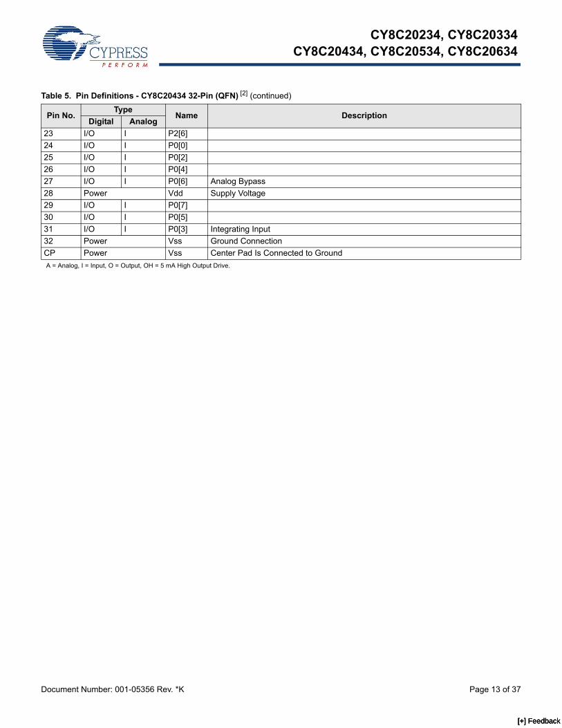
23 I/O I P2[6]24 I/O I P0[0]25 I/O I P0[2]26 I/O I P0[4]27 I/O I P0[6] Analog Bypass28 Power Vdd Supply Voltage29 I/O I P0[7]30 I/O I P0[5]31 I/O I P0[3] Integrating Input32 Power Vss Ground ConnectionCP Power Vss Center Pad Is Connected to Ground A = Analog, I = Input, O = Output, OH = 5 mA High Output Drive.
Table 5. Pin Definitions - CY8C20434 32-Pin (QFN) [2] (continued)
Pin No.Type
Name DescriptionDigital Analog
[+] Feedback [+] Feedback [+] Feedback
CY8C20234, CY8C20334CY8C20434, CY8C20534, CY8C20634
Document Number: 001-05356 Rev. *K Page 14 of 37
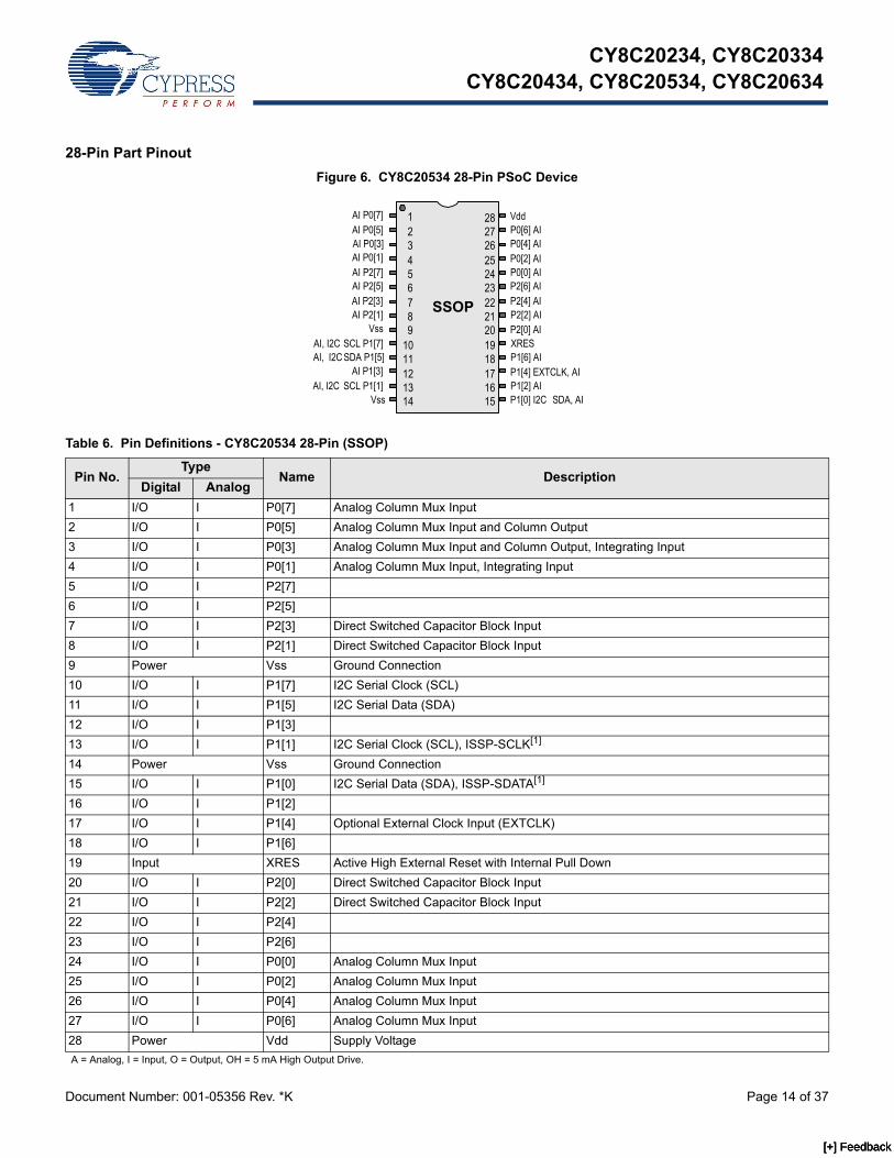
28-Pin Part PinoutFigure 6. CY8C20534 28-Pin PSoC Device
AI P0[7]AI P0[5]AI P0[3]AI P0[1]AI P2[7]AI P2[5]AI P2[3] SSOP
123456789
1011121314
2827262524232221201918171615
AI P2[1]Vss
Vss
AI P1[3]
AI, I2C SCL P1[7]AI, I2C SDA P1[5]
SCL P1[1]AI, I2C
VddP0[6] AIP0[4] AIP0[2] AIP0[0] AIP2[6] AIP2[4] AIP2[2] AIP2[0] AIXRESP1[6] AIP1[4] EXTCLK, AI P1[2] AIP1[0] I2C SDA, AI
Table 6. Pin Definitions - CY8C20534 28-Pin (SSOP)
Pin No.Type
Name DescriptionDigital Analog
1 I/O I P0[7] Analog Column Mux Input2 I/O I P0[5] Analog Column Mux Input and Column Output3 I/O I P0[3] Analog Column Mux Input and Column Output, Integrating Input4 I/O I P0[1] Analog Column Mux Input, Integrating Input5 I/O I P2[7]6 I/O I P2[5]7 I/O I P2[3] Direct Switched Capacitor Block Input8 I/O I P2[1] Direct Switched Capacitor Block Input9 Power Vss Ground Connection10 I/O I P1[7] I2C Serial Clock (SCL)11 I/O I P1[5] I2C Serial Data (SDA)12 I/O I P1[3]13 I/O I P1[1] I2C Serial Clock (SCL), ISSP-SCLK[1]
14 Power Vss Ground Connection15 I/O I P1[0] I2C Serial Data (SDA), ISSP-SDATA[1]
16 I/O I P1[2]17 I/O I P1[4] Optional External Clock Input (EXTCLK)18 I/O I P1[6] 19 Input XRES Active High External Reset with Internal Pull Down20 I/O I P2[0] Direct Switched Capacitor Block Input21 I/O I P2[2] Direct Switched Capacitor Block Input22 I/O I P2[4]23 I/O I P2[6]24 I/O I P0[0] Analog Column Mux Input25 I/O I P0[2] Analog Column Mux Input26 I/O I P0[4] Analog Column Mux Input27 I/O I P0[6] Analog Column Mux Input28 Power Vdd Supply Voltage A = Analog, I = Input, O = Output, OH = 5 mA High Output Drive.
[+] Feedback [+] Feedback [+] Feedback
CY8C20234, CY8C20334CY8C20434, CY8C20534, CY8C20634
Document Number: 001-05356 Rev. *K Page 15 of 37
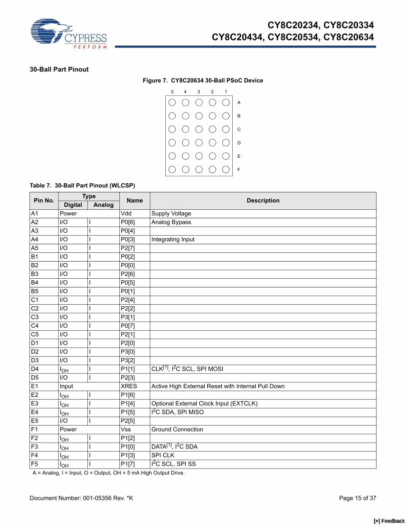
30-Ball Part PinoutFigure 7. CY8C20634 30-Ball PSoC Device
Table 7. 30-Ball Part Pinout (WLCSP)
Pin No.Type
Name DescriptionDigital Analog
A1 Power Vdd Supply VoltageA2 I/O I P0[6] Analog BypassA3 I/O I P0[4]A4 I/O I P0[3] Integrating InputA5 I/O I P2[7]B1 I/O I P0[2]B2 I/O I P0[0]B3 I/O I P2[6]B4 I/O I P0[5]B5 I/O I P0[1]C1 I/O I P2[4]C2 I/O I P2[2]C3 I/O I P3[1]C4 I/O I P0[7]C5 I/O I P2[1]D1 I/O I P2[0]D2 I/O I P3[0]D3 I/O I P3[2]D4 IOH I P1[1] CLK[1], I2C SCL, SPI MOSID5 I/O I P2[3]E1 Input XRES Active High External Reset with Internal Pull DownE2 IOH I P1[6]E3 IOH I P1[4] Optional External Clock Input (EXTCLK)E4 IOH I P1[5] I2C SDA, SPI MISOE5 I/O I P2[5]F1 Power Vss Ground ConnectionF2 IOH I P1[2]F3 IOH I P1[0] DATA[1], I2C SDAF4 IOH I P1[3] SPI CLKF5 IOH I P1[7] I2C SCL, SPI SS A = Analog, I = Input, O = Output, OH = 5 mA High Output Drive.
5 4 3 2 1
A
B
C
D
E
F
[+] Feedback [+] Feedback [+] Feedback
CY8C20234, CY8C20334CY8C20434, CY8C20534, CY8C20634
Document Number: 001-05356 Rev. *K Page 16 of 37
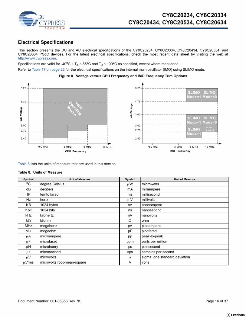
Electrical SpecificationsThis section presents the DC and AC electrical specifications of the CY8C20234, CY8C20334, CY8C20434, CY8C20534, and CY8C20634 PSoC devices. For the latest electrical specifications, check the most recent data sheet by visiting the web at http://www.cypress.com.Specifications are valid for -40oC ≤ TA ≤ 85oC and TJ ≤ 100oC as specified, except where mentioned.Refer to Table 17 on page 22 for the electrical specifications on the internal main oscillator (IMO) using SLIMO mode.
Figure 8. Voltage versus CPU Frequency and IMO Frequency Trim Options
Table 8 lists the units of measure that are used in this section.
Table 8. Units of Measure
Symbol Unit of Measure Symbol Unit of MeasureoC degree Celsius μW microwattsdB decibels mA milliamperefF femto farad ms millisecondHz hertz mV millivoltsKB 1024 bytes nA nanoampereKbit 1024 bits ns nanosecondkHz kilohertz nV nanovoltskΩ kilohm Ω ohm
MHz megahertz pA picoampereMΩ megaohm pF picofaradμA microampere pp peak-to-peakμF microfarad ppm parts per millionμH microhenry ps picosecondμs microsecond sps samples per secondμV microvolts σ sigma: one standard deviation
μVrms microvolts root-mean-square V volts
5.25
4.75
3.00
750 kHz 12 MHzCPU Frequency
Vdd
Volta
ge
5.25
4.75
3.00
750 kHz 6 MHz 12 MHzIMO Frequency
Vdd
Volta
ge
3.60
3 MHz
2.40
SLIMOMode=1
2.40
3 MHz
Valid
Operating
Region
SLIMOMode=1
SLIMOMode=0
SLIMOMode=1
SLIMOMode=0
2.70
SLIMOMode=1
SLIMOMode=0
2.70
6 MHz
[+] Feedback [+] Feedback [+] Feedback
CY8C20234, CY8C20334CY8C20434, CY8C20534, CY8C20634
Document Number: 001-05356 Rev. *K Page 17 of 37
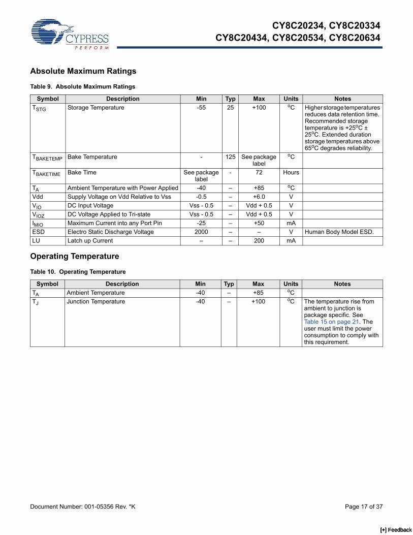
Absolute Maximum Ratings
Operating Temperature
Table 9. Absolute Maximum Ratings
Symbol Description Min Typ Max Units NotesTSTG Storage Temperature -55 25 +100 oC Higher storage temperatures
reduces data retention time. Recommended storage temperature is +25oC ± 25oC. Extended duration storage temperatures above 65oC degrades reliability.
TBAKETEMP Bake Temperature - 125 See package label
oC
TBAKETIME Bake Time See package label
- 72 Hours
TA Ambient Temperature with Power Applied -40 – +85 oCVdd Supply Voltage on Vdd Relative to Vss -0.5 – +6.0 VVIO DC Input Voltage Vss - 0.5 – Vdd + 0.5 VVIOZ DC Voltage Applied to Tri-state Vss - 0.5 – Vdd + 0.5 VIMIO Maximum Current into any Port Pin -25 – +50 mAESD Electro Static Discharge Voltage 2000 – – V Human Body Model ESD.LU Latch up Current – – 200 mA
Table 10. Operating Temperature
Symbol Description Min Typ Max Units NotesTA Ambient Temperature -40 – +85 oCTJ Junction Temperature -40 – +100 oC The temperature rise from
ambient to junction is package specific. See Table 15 on page 21. The user must limit the power consumption to comply with this requirement.
[+] Feedback [+] Feedback [+] Feedback
CY8C20234, CY8C20334CY8C20434, CY8C20534, CY8C20634
Document Number: 001-05356 Rev. *K Page 18 of 37
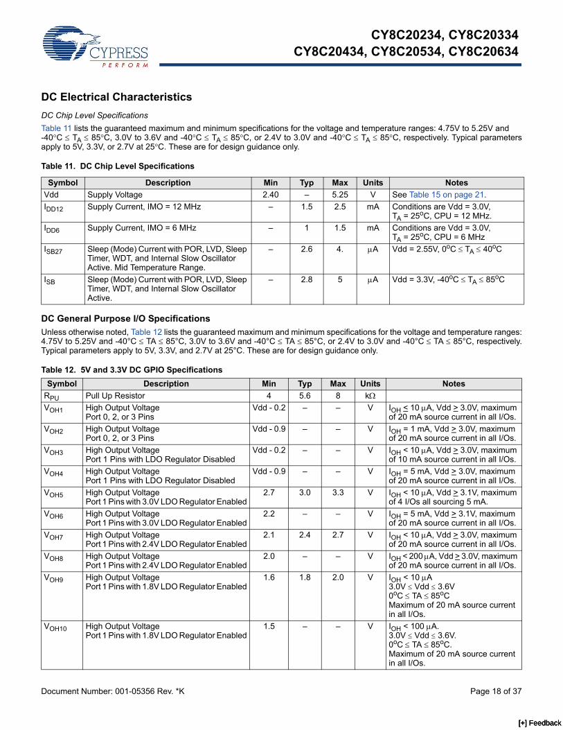
DC Electrical CharacteristicsDC Chip Level SpecificationsTable 11 lists the guaranteed maximum and minimum specifications for the voltage and temperature ranges: 4.75V to 5.25V and -40°C ≤ TA ≤ 85°C, 3.0V to 3.6V and -40°C ≤ TA ≤ 85°C, or 2.4V to 3.0V and -40°C ≤ TA ≤ 85°C, respectively. Typical parameters apply to 5V, 3.3V, or 2.7V at 25°C. These are for design guidance only.
DC General Purpose I/O SpecificationsUnless otherwise noted, Table 12 lists the guaranteed maximum and minimum specifications for the voltage and temperature ranges: 4.75V to 5.25V and -40°C ≤ TA ≤ 85°C, 3.0V to 3.6V and -40°C ≤ TA ≤ 85°C, or 2.4V to 3.0V and -40°C ≤ TA ≤ 85°C, respectively. Typical parameters apply to 5V, 3.3V, and 2.7V at 25°C. These are for design guidance only.
Table 11. DC Chip Level Specifications
Symbol Description Min Typ Max Units NotesVdd Supply Voltage 2.40 – 5.25 V See Table 15 on page 21.IDD12 Supply Current, IMO = 12 MHz – 1.5 2.5 mA Conditions are Vdd = 3.0V,
TA = 25oC, CPU = 12 MHz.IDD6 Supply Current, IMO = 6 MHz – 1 1.5 mA Conditions are Vdd = 3.0V,
TA = 25oC, CPU = 6 MHzISB27 Sleep (Mode) Current with POR, LVD, Sleep
Timer, WDT, and Internal Slow Oscillator Active. Mid Temperature Range.
– 2.6 4. μA Vdd = 2.55V, 0oC ≤ TA ≤ 40oC
ISB Sleep (Mode) Current with POR, LVD, Sleep Timer, WDT, and Internal Slow Oscillator Active.
– 2.8 5 μA Vdd = 3.3V, -40oC ≤ TA ≤ 85oC
Table 12. 5V and 3.3V DC GPIO Specifications Symbol Description Min Typ Max Units Notes
RPU Pull Up Resistor 4 5.6 8 kΩVOH1 High Output Voltage
Port 0, 2, or 3 PinsVdd - 0.2 – – V IOH < 10 μA, Vdd > 3.0V, maximum
of 20 mA source current in all I/Os.VOH2 High Output Voltage
Port 0, 2, or 3 PinsVdd - 0.9 – – V IOH = 1 mA, Vdd > 3.0V, maximum
of 20 mA source current in all I/Os.VOH3 High Output Voltage
Port 1 Pins with LDO Regulator DisabledVdd - 0.2 – – V IOH < 10 μA, Vdd > 3.0V, maximum
of 10 mA source current in all I/Os.VOH4 High Output Voltage
Port 1 Pins with LDO Regulator DisabledVdd - 0.9 – – V IOH = 5 mA, Vdd > 3.0V, maximum
of 20 mA source current in all I/Os.VOH5 High Output Voltage
Port 1 Pins with 3.0V LDO Regulator Enabled2.7 3.0 3.3 V IOH < 10 μA, Vdd > 3.1V, maximum
of 4 I/Os all sourcing 5 mA.VOH6 High Output Voltage
Port 1 Pins with 3.0V LDO Regulator Enabled2.2 – – V IOH = 5 mA, Vdd > 3.1V, maximum
of 20 mA source current in all I/Os.VOH7 High Output Voltage
Port 1 Pins with 2.4V LDO Regulator Enabled2.1 2.4 2.7 V IOH < 10 μA, Vdd > 3.0V, maximum
of 20 mA source current in all I/Os. VOH8 High Output Voltage
Port 1 Pins with 2.4V LDO Regulator Enabled2.0 – – V IOH < 200 μA, Vdd > 3.0V, maximum
of 20 mA source current in all I/Os.VOH9 High Output Voltage
Port 1 Pins with 1.8V LDO Regulator Enabled1.6 1.8 2.0 V IOH < 10 μA
3.0V ≤ Vdd ≤ 3.6V 0oC ≤ TA ≤ 85oC Maximum of 20 mA source current in all I/Os.
VOH10 High Output Voltage Port 1 Pins with 1.8V LDO Regulator Enabled
1.5 – – V IOH < 100 μA. 3.0V ≤ Vdd ≤ 3.6V. 0oC ≤ TA ≤ 85oC. Maximum of 20 mA source current in all I/Os.
[+] Feedback [+] Feedback [+] Feedback
CY8C20234, CY8C20334CY8C20434, CY8C20534, CY8C20634
Document Number: 001-05356 Rev. *K Page 19 of 37
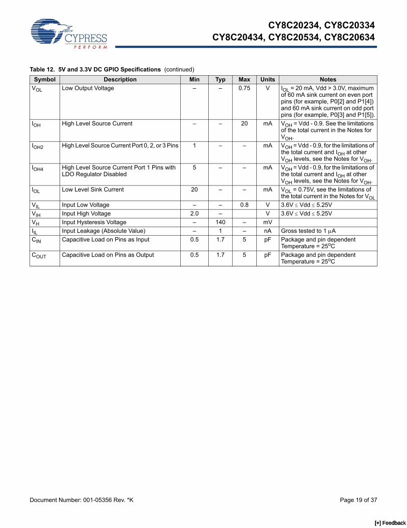
VOL Low Output Voltage – – 0.75 V IOL = 20 mA, Vdd > 3.0V, maximum of 60 mA sink current on even port pins (for example, P0[2] and P1[4]) and 60 mA sink current on odd port pins (for example, P0[3] and P1[5]).
IOH High Level Source Current – – 20 mA VOH = Vdd - 0.9. See the limitations of the total current in the Notes for VOH.
IOH2 High Level Source Current Port 0, 2, or 3 Pins 1 – – mA VOH = Vdd - 0.9, for the limitations of the total current and IOH at other VOH levels, see the Notes for VOH.
IOH4 High Level Source Current Port 1 Pins with LDO Regulator Disabled
5 – – mA VOH = Vdd - 0.9, for the limitations of the total current and IOH at other VOH levels, see the Notes for VOH.
IOL Low Level Sink Current 20 – – mA VOL = 0.75V, see the limitations of the total current in the Notes for VOL
VIL Input Low Voltage – – 0.8 V 3.6V ≤ Vdd ≤ 5.25VVIH Input High Voltage 2.0 – V 3.6V ≤ Vdd ≤ 5.25VVH Input Hysteresis Voltage – 140 – mVIIL Input Leakage (Absolute Value) – 1 – nA Gross tested to 1 μACIN Capacitive Load on Pins as Input 0.5 1.7 5 pF Package and pin dependent
Temperature = 25oCCOUT Capacitive Load on Pins as Output 0.5 1.7 5 pF Package and pin dependent
Temperature = 25oC
Table 12. 5V and 3.3V DC GPIO Specifications (continued)
Symbol Description Min Typ Max Units Notes
[+] Feedback [+] Feedback [+] Feedback
CY8C20234, CY8C20334CY8C20434, CY8C20534, CY8C20634
Document Number: 001-05356 Rev. *K Page 20 of 37
DC Analog Mux Bus Specifications
Table 14 lists the guaranteed maximum and minimum specifications for the voltage and temperature ranges: 4.75V to 5.25V and -40°C ≤ TA ≤ 85°C, 3.0V to 3.6V and -40°C ≤ TA ≤ 85°C, or 2.4V to 3.0V and -40°C ≤ TA ≤ 85°C, respectively. Typical parameters apply to 5V, 3.3V, or 2.7V at 25°C. These are for design guidance only.
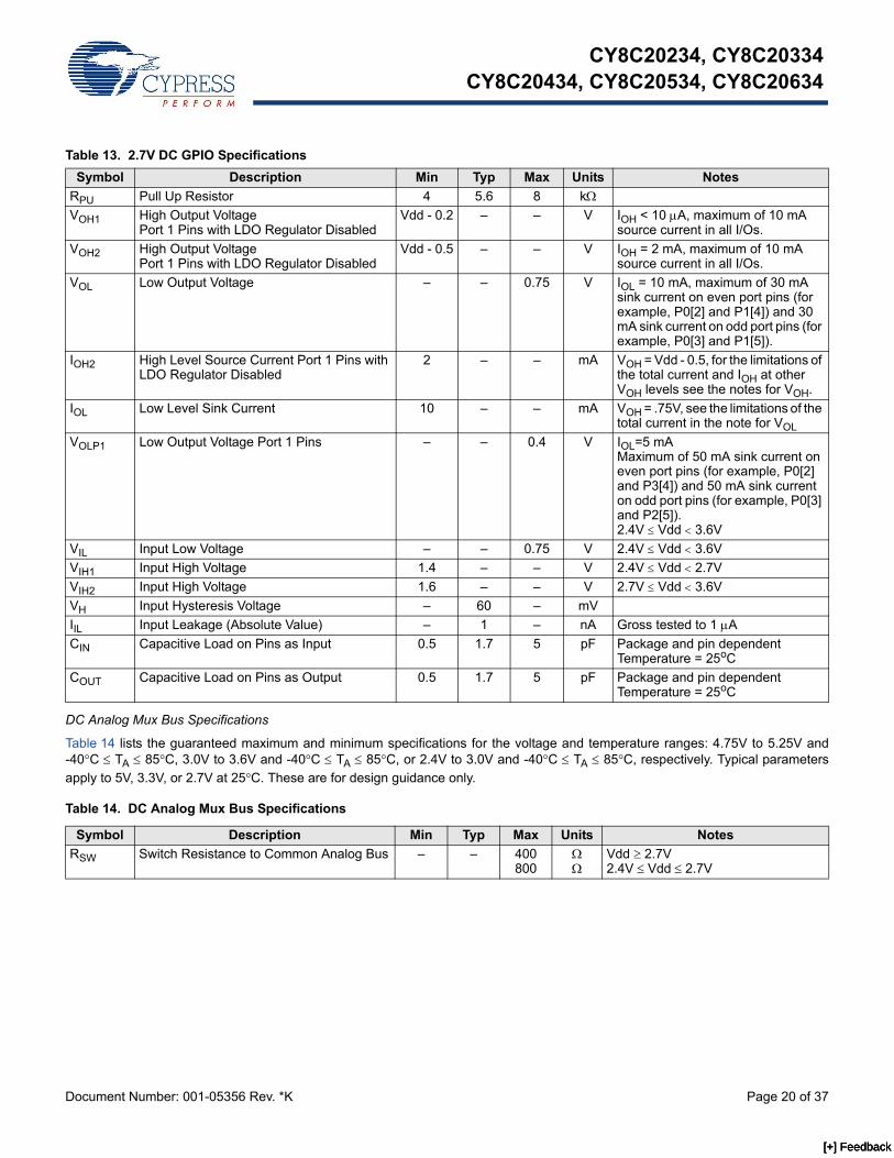
Table 13. 2.7V DC GPIO Specifications Symbol Description Min Typ Max Units Notes
RPU Pull Up Resistor 4 5.6 8 kΩVOH1 High Output Voltage
Port 1 Pins with LDO Regulator DisabledVdd - 0.2 – – V IOH < 10 μA, maximum of 10 mA
source current in all I/Os.VOH2 High Output Voltage
Port 1 Pins with LDO Regulator DisabledVdd - 0.5 – – V IOH = 2 mA, maximum of 10 mA
source current in all I/Os.VOL Low Output Voltage – – 0.75 V IOL = 10 mA, maximum of 30 mA
sink current on even port pins (for example, P0[2] and P1[4]) and 30 mA sink current on odd port pins (for example, P0[3] and P1[5]).
IOH2 High Level Source Current Port 1 Pins with LDO Regulator Disabled
2 – – mA VOH = Vdd - 0.5, for the limitations of the total current and IOH at other VOH levels see the notes for VOH.
IOL Low Level Sink Current 10 – – mA VOH = .75V, see the limitations of the total current in the note for VOL
VOLP1 Low Output Voltage Port 1 Pins – – 0.4 V IOL=5 mAMaximum of 50 mA sink current on even port pins (for example, P0[2] and P3[4]) and 50 mA sink current on odd port pins (for example, P0[3] and P2[5]).2.4V ≤ Vdd < 3.6V
VIL Input Low Voltage – – 0.75 V 2.4V ≤ Vdd < 3.6VVIH1 Input High Voltage 1.4 – – V 2.4V ≤ Vdd < 2.7VVIH2 Input High Voltage 1.6 – – V 2.7V ≤ Vdd < 3.6VVH Input Hysteresis Voltage – 60 – mVIIL Input Leakage (Absolute Value) – 1 – nA Gross tested to 1 μACIN Capacitive Load on Pins as Input 0.5 1.7 5 pF Package and pin dependent
Temperature = 25oCCOUT Capacitive Load on Pins as Output 0.5 1.7 5 pF Package and pin dependent
Temperature = 25oC
Table 14. DC Analog Mux Bus Specifications
Symbol Description Min Typ Max Units NotesRSW Switch Resistance to Common Analog Bus – – 400
800ΩΩ
Vdd ≥ 2.7V 2.4V ≤ Vdd ≤ 2.7V
[+] Feedback [+] Feedback [+] Feedback

CY8C20234, CY8C20334CY8C20434, CY8C20534, CY8C20634
Document Number: 001-05356 Rev. *K Page 21 of 37
DC POR and LVD Specifications
Table 15 lists the guaranteed maximum and minimum specifications for the voltage and temperature ranges: 4.75V to 5.25V and -40°C ≤ TA ≤ 85°C, 3.0V to 3.6V and -40°C ≤ TA ≤ 85°C, or 2.4V to 3.0V and -40°C ≤ TA ≤ 85°C, respectively. Typical parameters apply to 5V, 3.3V, or 2.7V at 25°C. These are for design guidance only.
DC Programming Specifications
Table 16 lists the guaranteed minimum and maximum specifications for the voltage and temperature ranges: 4.75V to 5.25V and -40°C ≤ TA ≤ 85°C, 3.0V to 3.6V and -40°C ≤ TA ≤ 85°C, or 2.4V to 3.0V and -40°C ≤ TA ≤ 85°C, respectively. Typical parameters apply to 5V, 3.3V, or 2.7V at 25°C. These are for design guidance only. Flash Endurance and Retention specifications with the use of the EEPROM User Module are valid only within the range: 25°C +/-20C during the Flash Write operation. Reference the EEPROM User Module data sheet instructions for EEPROM Flash Write requirements outside of the 25°C +/-20°C temperature window.
Table 15. DC POR and LVD Specifications Symbol Description Min Typ Max Units Notes
VPPOR0VPPOR1VPPOR2
Vdd Value for PPOR TripPORLEV[1:0] = 00bPORLEV[1:0] = 01bPORLEV[1:0] = 10b
–––
2.362.602.82
2.402.652.95
VVV
Vdd is greater than or equal to 2.5V during startup, reset from the XRES pin, or reset from Watchdog.
VLVD0VLVD1VLVD2VLVD3VLVD4VLVD5VLVD6VLVD7
Vdd Value for LVD TripVM[2:0] = 000bVM[2:0] = 001bVM[2:0] = 010bVM[2:0] = 011bVM[2:0] = 100bVM[2:0] = 101bVM[2:0] = 110bVM[2:0] = 111b
2.392.542.752.852.96
––
4.52
2.452.712.923.023.13
––
4.73
2.51[3]
2.78[4]
2.99[5]
3.093.20
––
4.83
V
VVVVVVV
Notes3. Always greater than 50 mV above VPPOR (PORLEV = 00) for falling supply.4. Always greater than 50 mV above VPPOR (PORLEV = 01) for falling supply.5. Always greater than 50 mV above VPPOR (PORLEV = 10) for falling supply.6. A maximum of 36 x 50,000 block endurance cycles is allowed. This is balanced between operations on 36x1 blocks of 50,000 maximum cycles each, 36x2 blocks of
25,000 maximum cycles each, or 36x4 blocks of 12,500 maximum cycles each (to limit the total number of cycles to 36x50,000 and that no single block ever sees more than 50,000 cycles).
7. The 50,000 cycle flash endurance per block will only be guaranteed if the flash is operating within one voltage range. Voltage ranges are 2.4V to 3.0V, 3.0V to 3.6V and 4.75V to 5.25V.
Table 16. DC Programming Specifications
Symbol Description Min Typ Max Units NotesVddIWRITE Supply Voltage for Flash Write Operations 2.70 – – VIDDP Supply Current During Programming or
Verify– 5 25 mA
VILP Input Low Voltage During Programming or Verify
– – 0.8 V
VIHP Input High Voltage During Programming or Verify
2.2 – – V
IILP Input Current when Applying Vilp to P1[0] or P1[1] During Programming or Verify
– – 0.2 mA Driving internal pull down resistor.
IIHP Input Current when Applying Vihp to P1[0] or P1[1] During Programming or Verify
– – 1.5 mA Driving internal pull down resistor.
VOLV Output Low Voltage During Programming or Verify
– – Vss + 0.75 V
VOHV Output High Voltage During Programming or Verify
Vdd –1.0 – Vdd V
FlashENPB Flash Endurance (per block) 50,000[7] – – – Erase/write cycles per block.FlashENT Flash Endurance (total)[6] 1,800,000 – – – Erase/write cycles.FlashDR Flash Data Retention 10 – – Year
s
[+] Feedback [+] Feedback [+] Feedback
CY8C20234, CY8C20334CY8C20434, CY8C20534, CY8C20634
Document Number: 001-05356 Rev. *K Page 22 of 37
AC Electrical CharacteristicsAC Chip Level SpecificationsTable 17, Table 18, and Table 19 list the guaranteed maximum and minimum specifications for the voltage and temperature ranges: 4.75V to 5.25V and -40°C ≤ TA ≤ 85°C, 3.0V to 3.6V and -40°C ≤ TA ≤ 85°C, or 2.4V to 3.0V and -40°C ≤ TA ≤ 85°C respectively. Typical parameters apply to 5V, 3.3V, or 2.7V at 25°C. These are for design guidance only.
Table 17. 5V and 3.3V AC Chip-Level Specifications
Symbol Description Min Typ Max Units NotesFCPU1 CPU Frequency (3.3V Nominal) 0.75 – 12.6 MHz 12 MHz only for SLIMO Mode = 0F32K1 Internal Low Speed Oscillator Frequency 15 32 64 kHzF32K_U Internal Low Speed Oscillator (ILO) Untrimmed
Frequency5 – – kHz After a reset and before the M8C starts
to run, the ILO is not trimmed. See the System Resets section of the PSoC Technical Reference Manual for details on this timing.
FIMO12 Internal Main Oscillator Stability for 12 MHz (Commercial Temperature)[8]
11.4 12 12.6 MHz Trimmed for 3.3V operation using factory trim values. See Figure 8 on page 16, SLIMO Mode = 0.
FIMO6 Internal Main Oscillator Stability for 6 MHz (Commercial Temperature)
5.5 6.0 6.5 MHz Trimmed for 3.3V operation using factory trim values. See Figure 8 on page 16, SLIMO Mode = 1.
DCIMO Duty Cycle of IMO 40 50 60 %DCILO Internal Low Speed Oscillator Duty Cycle 20 50 80 %TXRST External Reset Pulse Width 10 – – μsTPOWERUP Time from end of POR to CPU executing code – 16 100 ms Power up from 0V. See the System
Resets section of the PSoC Technical Reference Manual.
SRPOWER_UP
Power Supply Slew Rate – – 250 V/ms When Vdd remains in the range from 1.71V to 1.9V for more than 50 µsec, the slew rate when moving from the 1.71V to 1.9V range to greater than 2V must be slower than 1V/500 µsec to avoid triggering POR. The only other restriction on slew rates for any other voltage range or transition is the SRPOWER_UP parameter.
Table 18. 2.7V AC Chip Level Specifications
Symbol Description Min Typ Max Units NotesFCPU1 CPU Frequency (2.7V Nominal) 0.75 – 3.25 MHzF32K1 Internal Low Speed Oscillator Frequency 8 32 96 kHzF32K_U Internal Low Speed Oscillator (ILO) Untrimmed
Frequency5 – – kHz After a reset and before the M8C starts
to run, the ILO is not trimmed. See the System Resets section of the PSoC Technical Reference Manual for details on this timing.
FIMO12 Internal Main Oscillator Stability for 12 MHz (Commercial Temperature)[8]
11.0 12 12.9 MHz Trimmed for 2.7V operation using factory trim values. See Figure 8 on page 16, SLIMO Mode = 0.
FIMO6 Internal Main Oscillator Stability for 6 MHz (Commercial Temperature)
5.5 6.0 6.5 MHz Trimmed for 2.7V operation using factory trim values. See Figure 8 on page 16, SLIMO Mode = 1.
DCIMO Duty Cycle of IMO 40 50 60 %DCILO Internal Low Speed Oscillator Duty Cycle 20 50 80 %
Note8. 0 to 70 °C ambient, Vdd = 3.3 V.
[+] Feedback [+] Feedback [+] Feedback
CY8C20234, CY8C20334CY8C20434, CY8C20534, CY8C20634
Document Number: 001-05356 Rev. *K Page 23 of 37
AC General Purpose I/O SpecificationsTable 19 and Table 20 list the guaranteed maximum and minimum specifications for the voltage and temperature ranges: 4.75V to 5.25V and -40°C ≤ TA ≤ 85°C, 3.0V to 3.6V and -40°C ≤ TA ≤ 85°C, or 2.4V to 3.0V and -40°C ≤ TA ≤ 85°C respectively. Typical parameters apply to 5V, 3.3V, or 2.7V at 25°C. These are for design guidance only.
Figure 9. GPIO Timing Diagram
TXRST External Reset Pulse Width 10 – – μsTPOWERUP Time from end of POR to CPU executing code – 16 100 ms Power up from 0V. See the System
Resets section of the PSoC Technical Reference Manual.
SRPOWER_UP
Power Supply Slew Rate – – 250 V/ms When Vdd remains in the range from 1.71V to 1.9V for more than 50 µsec, the slew rate when moving from the 1.71V to 1.9V range to greater than 2V must be slower than 1V/500 µsec to avoid triggering POR. The only other restriction on slew rates for any other voltage range or transition is the SRPOWER_UP parameter.
Table 19. 5V and 3.3V AC GPIO Specifications
Symbol Description Min Typ Max Units NotesFGPIO GPIO Operating Frequency 0 – 6 MHz Normal Strong Mode, Port 1.TRise023 Rise Time, Strong Mode, Cload = 50 pF
Ports 0, 2, 315 – 80 ns Vdd = 3.0 to 3.6V and 4.75V to 5.25V,
10% - 90%TRise1 Rise Time, Strong Mode, Cload = 50 pF
Port 110 – 50 ns Vdd = 3.0 to 3.6V, 10% - 90%
TFall Fall Time, Strong Mode, Cload = 50 pF All Ports
10 – 50 ns Vdd = 3.0 to 3.6V and 4.75V to 5.25V, 10% - 90%
Table 20. 2.7V AC GPIO Specifications
Symbol Description Min Typ Max Units NotesFGPIO GPIO Operating Frequency 0 – 1.5 MHz Normal Strong Mode, Port 1.TRise023 Rise Time, Strong Mode, Cload = 50 pF
Ports 0, 2, 315 – 100 ns Vdd = 2.4 to 3.0V, 10% - 90%
TRise1 Rise Time, Strong Mode, Cload = 50 pF Port 1
10 – 70 ns Vdd = 2.4 to 3.0V, 10% - 90%
TFall Fall Time, Strong Mode, Cload = 50 pF All Ports
10 – 70 ns Vdd = 2.4 to 3.0V, 10% - 90%
Table 18. 2.7V AC Chip Level Specifications (continued)
Symbol Description Min Typ Max Units Notes
TFallTRise023TRise1
90%
10%
GPIOPin
OutputVoltage
[+] Feedback [+] Feedback [+] Feedback
CY8C20234, CY8C20334CY8C20434, CY8C20534, CY8C20634
Document Number: 001-05356 Rev. *K Page 24 of 37
AC Comparator Amplifier SpecificationsTable 21 lists the guaranteed maximum and minimum specifications for the voltage and temperature ranges: 4.75V to 5.25V and -40°C ≤ TA ≤ 85°C, 3.0V to 3.6V and -40°C ≤ TA ≤ 85°C, or 2.4V to 3.0V and -40°C ≤ TA ≤ 85°C, respectively. Typical parameters apply to 5V, 3.3V, or 2.7V at 25°C. These are for design guidance only.
AC External Clock Specifications
Table 22, Table 23, Table 24, and Table 25 list the guaranteed maximum and minimum specifications for the voltage and tempera-ture ranges: 4.75V to 5.25V and -40°C ≤ TA ≤ 85°C, 3.0V to 3.6V and -40°C ≤ TA ≤ 85°C, or 2.4V to 3.0V and -40°C ≤ TA ≤ 85°C, respectively. Typical parameters apply to 5V, 3.3V, or 2.7V at 25°C. These are for design guidance only.
Table 21. AC Operational Amplifier Specifications
Symbol Description Min Typ Max Units NotesTCOMP Comparator Response Time, 50 mV
Overdrive100200
nsns
Vdd ≥ 3.0V. 2.4V < Vcc < 3.0V.
Table 22. 5V AC External Clock Specifications
Symbol Description Min Typ Max Units NotesFOSCEXT Frequency 0.750 – 12.6 MHz– High Period 38 – 5300 ns– Low Period 38 – – ns– Power Up IMO to Switch 150 – – μs
Table 23. 3.3V AC External Clock Specifications
Symbol Description Min Typ Max Units NotesFOSCEXT Frequency with CPU Clock divide by 1 0.750 – 12.6 MHz Maximum CPU frequency is 12 MHz
at 3.3V. With the CPU clock divider set to 1, the external clock must adhere to the maximum frequency and duty cycle requirements.
– High Period with CPU Clock divide by 1 41.7 – 5300 ns– Low Period with CPU Clock divide by 1 41.7 – – ns– Power Up IMO to Switch 150 – – μs
[+] Feedback [+] Feedback [+] Feedback
CY8C20234, CY8C20334CY8C20434, CY8C20534, CY8C20634
Document Number: 001-05356 Rev. *K Page 25 of 37
Table 24. 2.7V (Nominal) AC External Clock Specifications
Symbol Description Min Typ Max Units NotesFOSCEXT Frequency with CPU Clock divide by 1 0.750 – 3.080 MHz Maximum CPU frequency is 3 MHz at
2.7V. With the CPU clock divider set to 1, the external clock must adhere to the maximum frequency and duty cycle requirements.
FOSCEXT Frequency with CPU Clock divide by 2 or greater
0.15 – 6.35 MHz If the frequency of the external clock is greater than 3 MHz, the CPU clock divider is set to 2 or greater. In this case, the CPU clock divider ensures that the fifty percent duty cycle requirement is met.
– High Period with CPU Clock divide by 1 160 – 5300 ns– Low Period with CPU Clock divide by 1 160 – – ns– Power Up IMO to Switch 150 – – μs
Table 25. 2.7V (Minimum) AC External Clock Specifications
Symbol Description Min Typ Max Units NotesFOSCEXT Frequency with CPU Clock divide by 1 0.750 – 6.30 MHz Maximum CPU frequency is 6 MHz at
2.7V. With the CPU clock divider set to 1, the external clock must adhere to the maximum frequency and duty cycle requirements.
FOSCEXT Frequency with CPU Clock divide by 2 or greater
0.15 – 12.6 MHz If the frequency of the external clock is greater than 6 MHz, the CPU clock divider is set to 2 or greater. In this case, the CPU clock divider ensures that the fifty percent duty cycle requirement is met.
– High Period with CPU Clock divide by 1 160 – 5300 ns– Low Period with CPU Clock divide by 1 160 – – ns– Power Up IMO to Switch 150 – – μs
[+] Feedback [+] Feedback [+] Feedback

CY8C20234, CY8C20334CY8C20434, CY8C20534, CY8C20634
Document Number: 001-05356 Rev. *K Page 26 of 37
AC Programming SpecificationsTable 26 lists the guaranteed maximum and minimum specifications for the voltage and temperature ranges: 4.75V to 5.25V and -40°C ≤ TA ≤ 85°C, 3.0V to 3.6V and -40°C ≤ TA ≤ 85°C, or 2.4V to 3.0V and -40°C ≤ TA ≤ 85°C respectively. Typical parameters apply to 5V, 3.3V, or 2.7V at 25°C. These are for design guidance only.
AC I2C SpecificationsTable 27 and Table 28 list the guaranteed maximum and minimum specifications for the voltage and temperature ranges: 4.75V to 5.25V and -40°C ≤ TA ≤ 85°C, 3.0V to 3.6V and -40°C ≤ TA ≤ 85°C, or 2.4V to 3.0V and -40°C ≤ TA ≤ 85°C respectively. Typical parameters apply to 5V, 3.3V, or 2.7V at 25°C. These are for design guidance only.
Table 26. AC Programming Specifications
Symbol Description Min Typ Max Units NotesTRSCLK Rise Time of SCLK 1 – 20 nsTFSCLK Fall Time of SCLK 1 – 20 nsTSSCLK Data Set up Time to Falling Edge of SCLK 40 – – nsTHSCLK Data Hold Time from Falling Edge of SCLK 40 – – nsFSCLK Frequency of SCLK 0 – 8 MHzTERASEB Flash Erase Time (Block) – 10 – msTWRITE Flash Block Write Time – 40 – msTDSCLK Data Out Delay from Falling Edge of SCLK – – 45 ns 3.6 < VddTDSCLK3 Data Out Delay from Falling Edge of SCLK – – 50 ns 3.0 ≤ Vdd ≤ 3.6TDSCLK2 Data Out Delay from Falling Edge of SCLK – – 70 ns 2.4 ≤ Vdd ≤ 3.0TERASEALL Flash Erase Time (Bulk) – 20 – ms Erase all blocks and protection
fields at onceTPROGRAM_HOT Flash Block Erase + Flash Block Write Time – – 100 ms 0°C <= Tj <= 100°CTPROGRAM_COLD Flash Block Erase + Flash Block Write Time – – 200 ms -40°C <= Tj <= 0°C
Note9. A Fast Mode I2C bus device is used in a Standard Mode I2C bus system but the requirement tSU; DAT Š 250 ns is met. This automatically is the case if the device
does not stretch the LOW period of the SCL signal. If such device does stretch the LOW period of the SCL signal, it must output the next data bit to the SDA line trmax + tSU; DAT = 1000 + 250 = 1250 ns (according to the Standard Mode I2C bus specification) before the SCL line is released.
Table 27. AC Characteristics of the I2C SDA and SCL Pins for Vdd ≥ 3.0V
Symbol DescriptionStandard Mode Fast Mode
UnitsMin Max Min Max
FSCLI2C SCL Clock Frequency 0 100 0 400 kHz
THDSTAI2C Hold Time (repeated) START Condition. After this period, the first clock pulse is generated
4.0 – 0.6 – μs
TLOWI2C LOW Period of the SCL Clock 4.7 – 1.3 – μs
THIGHI2C HIGH Period of the SCL Clock 4.0 – 0.6 – μs
TSUSTAI2C Setup Time for a Repeated START Condition
4.7 – 0.6 – μs
THDDATI2C Data Hold Time 0 – 0 – μs
TSUDATI2C Data Setup Time 250 – 100[9] – ns
TSUSTOI2C Setup Time for STOP Condition 4.0 – 0.6 – μs
TBUFI2C Bus Free Time Between a STOP and START Condition
4.7 – 1.3 – μs
TSPI2C Pulse Width of spikes are suppressed by the input filter
– – 0 50 ns
[+] Feedback [+] Feedback [+] Feedback
CY8C20234, CY8C20334CY8C20434, CY8C20534, CY8C20634
Document Number: 001-05356 Rev. *K Page 27 of 37
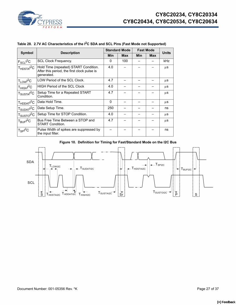
Figure 10. Definition for Timing for Fast/Standard Mode on the I2C Bus
Table 28. 2.7V AC Characteristics of the I2C SDA and SCL Pins (Fast Mode not Supported)
Symbol DescriptionStandard Mode Fast Mode
UnitsMin Max Min Max
FSCLI2C SCL Clock Frequency. 0 100 – – kHz
THDSTAI2C Hold Time (repeated) START Condition. After this period, the first clock pulse is generated.
4.0 – – – μs
TLOWI2C LOW Period of the SCL Clock. 4.7 – – – μs
THIGHI2C HIGH Period of the SCL Clock 4.0 – – – μs
TSUSTAI2C Setup Time for a Repeated START Condition.
4.7 – – – μs
THDDATI2C Data Hold Time. 0 – – – μs
TSUDATI2C Data Setup Time. 250 – – – ns
TSUSTOI2C Setup Time for STOP Condition. 4.0 – – – μs
TBUFI2C Bus Free Time Between a STOP and START Condition.
4.7 – – – μs
TSPI2C Pulse Width of spikes are suppressed by the input filter.
– – – – ns
SDA
SCL
S Sr SP
TBUFI2C
TSPI2CTHDSTAI2C
TSUSTOI2CTSUSTAI2C
TLOWI2C
THIGHI2CTHDDATI2CTHDSTAI2C
TSUDATI2C
[+] Feedback [+] Feedback [+] Feedback
CY8C20234, CY8C20334CY8C20434, CY8C20534, CY8C20634
Document Number: 001-05356 Rev. *K Page 28 of 37
Table 29. SPI Master AC Specifications
Symbol Parameter Conditions Min Typ Max UnitsFSCLK SCLK clock frequency 12 MHz
DC SCLK duty cycle 50 %
TSETUP MISO to SCLK setup time 40 ns
THOLD SCLK to MISO hold time 40 ns
TOUT_VAL SCLK to MOSI valid time 40 ns
TOUT_HIGH MOSI high time 40 ns
Table 30. SPI Slave AC Specifications
Symbol Parameter Conditions Min Typ Max UnitsTSCLK SCLK clock frequency 12 MHz
TLOW SCLK low time 41.67 ns
THIGH SCLK high time 41.67 ns
TSETUP MOSI to SCLK setup time 30 ns
THOLD SCLK to MOSI hold time 50 ns
TSS_MISO SS high to MISO valid 153 ns
TSCLK_MISO SCLK to MISO valid 125 ns
TSS_HIGH SS high time 50 ns
TSS_CLK Time from SS low to first SCLK
2/SCLK ns
TCLK_SS Time from last SCLK to SS high
2/SCLK ns
[+] Feedback [+] Feedback [+] Feedback

CY8C20234, CY8C20334CY8C20434, CY8C20534, CY8C20634
Document Number: 001-05356 Rev. *K Page 29 of 37
Packaging DimensionsThis section illustrates the packaging specifications for the CY8C20234, CY8C20334, CY8C20434, CY8C20534, and CY8C20634PSoC devices along with the thermal impedances for each package.Important Note Emulation tools may require a larger area on the target PCB than the chip's footprint. For a detailed description of the emulation tools' dimensions, refer to the emulator pod drawings at http://www.cypress.com.
Figure 11. 48-Pin (7 x 7 x 1.0 mm) QFN
TOP VIEW
0.80 DIA.
6.70
6.90
C
1.00 MAX.
N
BOTTOM VIEW
SEATINGPLANE
N
22
0.23±0.05
0.50
1 1
0.08
0°-12°
0.30-0.45
0.05 MAX.
C
0.20 REF.0.80 MAX.
PIN1 ID
5.45
0.42±0.18(4X)
SIDE VIEW
7.10
6.80
6.706.80
7.106.90
5.55
5.455.55
0.20 R.
0.45
5.1
5.1
1. HATCH AREA IS SOLDERABLE EXPOSED METAL.
2. REFERENCE JEDEC#: MO-220
4. ALL DIMENSIONS ARE IN MM [MIN/MAX]
NOTES:
PART #
LEAD FREESTANDARD
LY48A
5. PACKAGE CODE
DESCRIPTION
3. PACKAGE WEIGHT: 0.13g
LF48A
PAD EXPOSED
SOLDERABLE
001-12919 *B
[+] Feedback [+] Feedback [+] Feedback
CY8C20234, CY8C20334CY8C20434, CY8C20534, CY8C20634
Document Number: 001-05356 Rev. *K Page 30 of 37
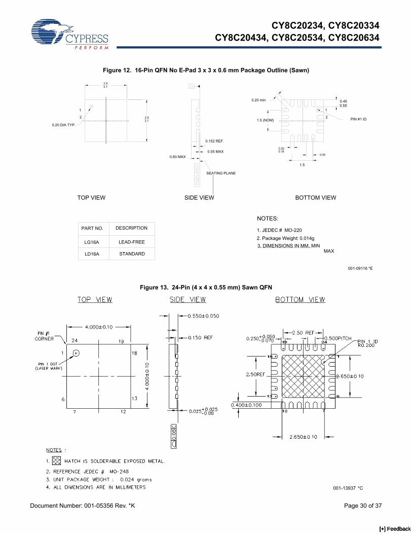
Figure 12. 16-Pin QFN No E-Pad 3 x 3 x 0.6 mm Package Outline (Sawn)
Figure 13. 24-Pin (4 x 4 x 0.55 mm) Sawn QFN
001-09116 *E
1.5
1.5 (NOM) PIN #1 ID
1
2
0.20 min 0.450.55
0.300.18
0.50
3. DIMENSIONS IN MM, MINMAX
BOTTOM VIEW
1. JEDEC # MO-2202. Package Weight: 0.014g
PART NO.
LG16A
LD16A
DESCRIPTION
LEAD-FREE
STANDARD
0.20 DIA TYP.
TOP VIEW
0.60 MAX0.05 MAX
0.152 REF.
SEATING PLANE
SIDE VIEW
2.9 3.1
2.9 3.1
NOTES:
1
2
001-13937 *C
[+] Feedback [+] Feedback [+] Feedback
CY8C20234, CY8C20334CY8C20434, CY8C20534, CY8C20634
Document Number: 001-05356 Rev. *K Page 31 of 37
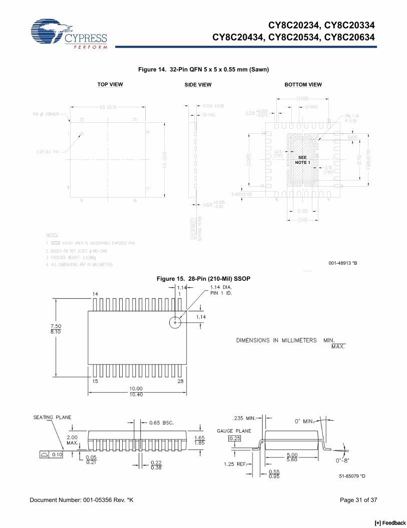
Figure 14. 32-Pin QFN 5 x 5 x 0.55 mm (Sawn)
Figure 15. 28-Pin (210-Mil) SSOP
001-48913 *B
51-85079 *D
[+] Feedback [+] Feedback [+] Feedback

CY8C20234, CY8C20334CY8C20434, CY8C20534, CY8C20634
Document Number: 001-05356 Rev. *K Page 32 of 37
Figure 16. 30-Ball (1.85 x 2.31 x 0.40 mm) WLCSP
Important Note For information on the preferred dimensions for mounting the QFN packages, see the application note “Application Notes for Surface Mount Assembly of Amkor's MicroLeadFrame (MLF) Packages” available at http://www.amkor.com.It is important to note that pinned vias for thermal conduction are not required for the low power 24, 32, and 48-pin QFN PSoC devices.
Thermal Impedances Table 31 illustrates the minimum solder reflow peak temperature to achieve good solderability.
Solder Reflow Peak TemperatureTable 32 illustrates the minimum solder reflow peak temperature to achieve good solderability.
001-44613 *A
Table 31. Thermal Impedances Per Package
Package Typical θJA [10]
16 QFN 46 oC/W24 QFN[11] 25 oC/W28 SSOP 96 oC/W30 WLCSP 54 °C/W32 QFN[11] 27 oC/W48 QFN[11] 28 oC/W
Table 32. Solder Reflow Peak TemperaturePackage Min Peak Temperature [12] Max Peak Temperature
16 QFN 240oC 260oC24 QFN 240oC 260oC28 SSOP 240oC 260oC30 WLCSP 217°C 220°C32 QFN 240oC 260oC48 QFN 240oC 260oC
Notes10. TJ = TA + Power x θJA.11. To achieve the thermal impedance specified for the QFN package, refer to "Application Notes for Surface Mount Assembly of Amkor's MicroLeadFrame (MLF)
Packages" available at http://www.cypress.com.12. Higher temperatures is required based on the solder melting point. Typical temperatures for solder are 220 ± 5oC with Sn-Pb or 245 ± 5oC with Sn-Ag-Cu paste.
Refer to the solder manufacturer specifications.
[+] Feedback [+] Feedback [+] Feedback
CY8C20234, CY8C20334CY8C20434, CY8C20534, CY8C20634
Document Number: 001-05356 Rev. *K Page 33 of 37
Development Tool SelectionSoftwarePSoC Designer™At the core of the PSoC development software suite is PSoC Designer, used to generate PSoC firmware applications. PSoC Designer is available free of charge at http://www.cypress.comand includes a free C compiler.
PSoC ProgrammerPSoC Programmer is flexible enough and is used on the bench in development and also suitable for factory programming. PSoC Programmer works either as a standalone programming application or operates directly from PSoC Designer. PSoC Programmer software is compatible with both PSoC ICE Cube In-Circuit Emulator and PSoC MiniProg. PSoC programmer is available free of charge at http://www.cypress.com.Development KitsAll development kits are sold at the Cypress Online Store.
CY3215-DK Basic Development KitThe CY3215-DK is for prototyping and development with PSoC Designer. This kit supports in-circuit emulation and the software interface enables users to run, halt, and single step the processor and view the content of specific memory locations. PSoC Designer supports the advance emulation features also. The kit includes:
■ PSoC Designer Software CD■ ICE-Cube In-Circuit Emulator
■ ICE Flex-Pod for CY8C29x66 Family
■ Cat-5 Adapter■ Mini-Eval Programming Board
■ 110 ~ 240V Power Supply, Euro-Plug Adapter■ iMAGEcraft C Compiler (Registration Required)■ ISSP Cable
■ USB 2.0 Cable and Blue Cat-5 Cable
■ 2 CY8C29466-24PXI 28-PDIP Chip Samples
Evaluation ToolsAll evaluation tools are sold at the Cypress Online Store.
CY3210-MiniProg1The CY3210-MiniProg1 kit enables the user to program PSoC devices via the MiniProg1 programming unit. The MiniProg is a small, compact prototyping programmer that connects to the PC via a provided USB 2.0 cable. The kit includes:
■ MiniProg Programming Unit
■ MiniEval Socket Programming and Evaluation Board
■ 28-Pin CY8C29466-24PXI PDIP PSoC Device Sample
■ 28-Pin CY8C27443-24PXI PDIP PSoC Device Sample
■ PSoC Designer Software CD
■ Getting Started Guide
■ USB 2.0 Cable
CY3210-PSoCEval1The CY3210-PSoCEval1 kit features an evaluation board and the MiniProg1 programming unit. The evaluation board includes an LCD module, potentiometer, LEDs, and plenty of bread-boarding space to meet all of your evaluation needs. The kit includes:
■ Evaluation Board with LCD Module
■ MiniProg Programming Unit
■ 28-Pin CY8C29466-24PXI PDIP PSoC Device Sample (2)
■ PSoC Designer Software CD
■ Getting Started Guide
■ USB 2.0 Cable
CY3214-PSoCEvalUSB The CY3214-PSoCEvalUSB evaluation kit features a devel-opment board for the CY8C24794-24LFXI PSoC device. Special features of the board include both USB and capacitive sensing development and debugging support. This evaluation board also includes an LCD module, potentiometer, LEDs, an enunciator and plenty of bread boarding space to meet all of your evaluation needs. The kit includes:
■ PSoCEvalUSB Board
■ LCD Module
■ MIniProg Programming Unit
■ Mini USB Cable
■ PSoC Designer and Example Projects CD
■ Getting Started Guide
■ Wire Pack
[+] Feedback [+] Feedback [+] Feedback
CY8C20234, CY8C20334CY8C20434, CY8C20534, CY8C20634
Document Number: 001-05356 Rev. *K Page 34 of 37
Device ProgrammersAll device programmers are purchased from the Cypress Online Store.
CY3216 Modular ProgrammerThe CY3216 Modular Programmer kit features a modular programmer and the MiniProg1 programming unit. The modular programmer includes three programming module cards and supports multiple Cypress products. The kit includes:
■ Modular Programmer Base
■ 3 Programming Module Cards
■ MiniProg Programming Unit
■ PSoC Designer Software CD
■ Getting Started Guide
■ USB 2.0 Cable
CY3207ISSP In-System Serial Programmer (ISSP)The CY3207ISSP is a production programmer. It includes protection circuitry and an industrial case that is more robust than the MiniProg in a production programming environment. Note that CY3207ISSP needs special software and is not compatible with PSoC Programmer. The kit includes:
■ CY3207 Programmer Unit
■ PSoC ISSP Software CD
■ 110 ~ 240V Power Supply, Euro-Plug Adapter
■ USB 2.0 Cable
Accessories (Emulation and Programming)
Table 33. Emulation and Programming Accessories
Part Number Pin Package Flex-Pod Kit [13] Foot Kit [14] Prototyping
Module Adapter [15]
CY8C20234-12LKXI 16 QFN Not Available CY3250-16QFN-FK CY3210-20X34 Not AvailableCY8C20334-12LQXI 24 QFN CY3250-20334QFN CY3250-24QFN-FK CY3210-20X34 AS-24-28-01ML-6CY8C20634-12FDXI 30 WLCSP Not Available CY3210-20X34 Not Available
Notes13. Dual function Digital I/O Pins also connect to the common analog mux.14. This part may be used for in-circuit debugging. It is NOT available for production.15. Programming adapter converts non-DIP package to DIP footprint. Specific details and ordering information for each of the adapters is available at
http://www.emulation.com.
[+] Feedback [+] Feedback [+] Feedback
CY8C20234, CY8C20334CY8C20434, CY8C20534, CY8C20634
Document Number: 001-05356 Rev. *K Page 35 of 37
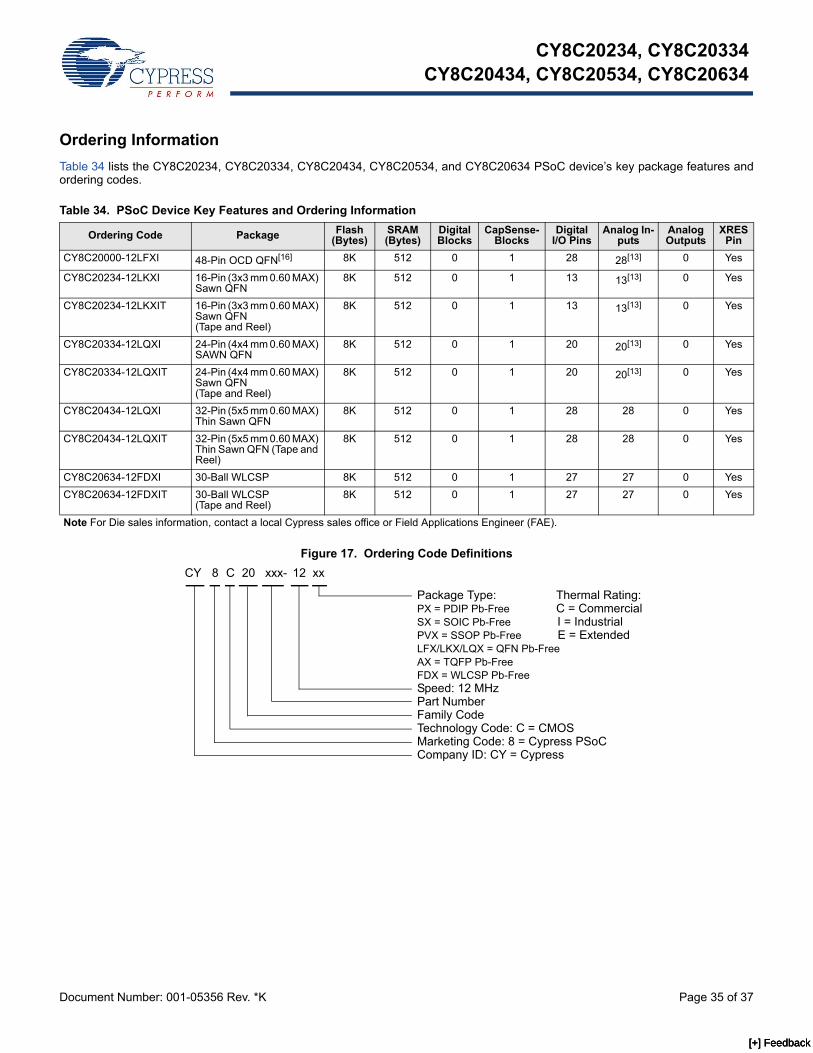
Ordering InformationTable 34 lists the CY8C20234, CY8C20334, CY8C20434, CY8C20534, and CY8C20634 PSoC device’s key package features and ordering codes.
Figure 17. Ordering Code Definitions
Table 34. PSoC Device Key Features and Ordering Information
Ordering Code Package Flash (Bytes)
SRAM (Bytes)
Digital Blocks
CapSense-Blocks
Digital I/O Pins
Analog In-puts
AnalogOutputs
XRES Pin
CY8C20000-12LFXI 48-Pin OCD QFN[16] 8K 512 0 1 28 28[13] 0 Yes
CY8C20234-12LKXI 16-Pin (3x3 mm 0.60 MAX) Sawn QFN
8K 512 0 1 13 13[13] 0 Yes
CY8C20234-12LKXIT 16-Pin (3x3 mm 0.60 MAX) Sawn QFN (Tape and Reel)
8K 512 0 1 13 13[13] 0 Yes
CY8C20334-12LQXI 24-Pin (4x4 mm 0.60 MAX) SAWN QFN
8K 512 0 1 20 20[13] 0 Yes
CY8C20334-12LQXIT 24-Pin (4x4 mm 0.60 MAX) Sawn QFN (Tape and Reel)
8K 512 0 1 20 20[13] 0 Yes
CY8C20434-12LQXI 32-Pin (5x5 mm 0.60 MAX) Thin Sawn QFN
8K 512 0 1 28 28 0 Yes
CY8C20434-12LQXIT 32-Pin (5x5 mm 0.60 MAX) Thin Sawn QFN (Tape and Reel)
8K 512 0 1 28 28 0 Yes
CY8C20634-12FDXI 30-Ball WLCSP 8K 512 0 1 27 27 0 YesCY8C20634-12FDXIT 30-Ball WLCSP
(Tape and Reel)8K 512 0 1 27 27 0 Yes
Note For Die sales information, contact a local Cypress sales office or Field Applications Engineer (FAE).
CY 8 C 20 xxx- 12 xx
Package Type: Thermal Rating: PX = PDIP Pb-Free C = Commercial SX = SOIC Pb-Free I = Industrial PVX = SSOP Pb-Free E = Extended LFX/LKX/LQX = QFN Pb-Free AX = TQFP Pb-Free FDX = WLCSP Pb-FreeSpeed: 12 MHzPart NumberFamily CodeTechnology Code: C = CMOSMarketing Code: 8 = Cypress PSoCCompany ID: CY = Cypress
[+] Feedback [+] Feedback [+] Feedback
CY8C20234, CY8C20334CY8C20434, CY8C20534, CY8C20634
Document Number: 001-05356 Rev. *K Page 36 of 37
Document History Page Document Title: CY8C20234, CY8C20334, CY8C20434, CY8C20534, CY8C20634 PSoC® Programmable System-on-ChipDocument Number: 001-05356
Rev. ECN Orig. of Change
Submission Date Description of Change
** 404571 HMT See ECN New silicon and document (Revision **).*A 418513 HMT See ECN Updated Electrical Specifications, including Storage Temperature and Maximum
Input Clock Frequency. Updated Features and Analog System Overview. Modified 32-pin QFN E-PAD dimensions. Added new 32-pin QFN. Add High Output Drive indicator to all P1[x] pinouts. Updated trademarks.
*B 490071 HMT See ECN Made data sheet “Final”. Added new Development Tool section. Added OCD pinout and package diagram. Added 16-pin QFN. Updated 24-pin and 32-pin QFN package diagrams to 0.60 MAX thickness. Changed from commercial to industrial temperature range. Updated Storage Temperature specification and notes. Updated thermal resistance data. Added development tool kit part numbers. Finetuned features and electrical specifications.
*C 788177 HMT See ECN Added CapSense SNR requirement reference. Added Low Power Comparator (LPC) AC/DC electrical specifications tables. Added 2.7V minimum specifications. Updated figure standards. Updated Technical Training paragraph. Added QFN package clarifications and dimensions. Updated ECN-ed Amkor dimensioned QFN package diagram revisions.
*D 1356805 HMT/SFVTMP3/HCL/SFV
See ECN Updated 24-pin QFN Theta JA. Added External Reset Pulse Width, TXRST, speci-fication. Fixed 48-pin QFN.vsd. Updated the table introduction and high output voltage description in section two. The sentence: "Exceeding maximum ratings may shorten the battery life of the device.” does not apply to all data sheets. Therefore, the word "battery" is changed to "useful.” Took out tabs after table and figure numbers in titles and added two hard spaces. Updated the section, DC General Purpose I/O Specifications on page 18 with new text. Updated VOH5 and VOH6 to say, ”High Output Voltage, Port 1 Pins with 3.0V LDO Regulator Enabled.” Updated VOH7 and VOH8 with the text, “maximum of 20 mA source current in all I/Os.”Added 28-pin SSOP part, pinout, package. Updated specs. Modified dev. tool part numbers.
*E 2197347 UVS/AESA See ECN Added 32-pin Sawn QFN Pin diagramRemoved package diagram: 32-Pin (5 X 5 mm) SAWN QFN(001-42168 *A)Updated Ordering Information table with CY8C20434-12LQXI and CY8C20434-12LQXIT ordering details.Corrected Table 16. DC Programming Specifications - Included above the table "Flash Endurance and Retention specifications with the use of the EEPROM User Module are valid only within the range: 25°C +/-20C during the Flash Write operation. Refer the EEPROM User Module data sheet instructions for EEPROM Flash Write requirements outside of the 25°C +/-20°C temperature window."
*F 2542938 RLRM/AESA 07/30/2008 Corrected Ordering Information format. Updated package diagrams 001-13937 and 001-30999. Updated data sheet template. Corrected Figure 6 (28-pin diagram).
*G 2610469 SNV/PYRS 11/20/08 Updated VOH5, VOH7, and VOH9 specifications*H 2693024 DPT/PYRS 04/16/2009 Changed title from PSoC® Mixed Signal Array to PSoC® Programmable
System-on-Chip™Replaced package outline drawing for 32-Pin Sawn QFNUpdated “Development Tool Selection” on page 33 Updated “Development Tools” on page 5 and “Designing with PSoC Designer” on page 6Updated “Getting Started” on page 4
*I 2717566 DRSW/AESA 06/11/2009 Updated AC Chip-Level, and AC Programming Specifications as follows: Modified FIMO6 (page 20), TWRITE specifications (page 23) Added IOH, IOL (page 17), Flash endurance note (page 19), DCILO (page 20), F32K_U (page 20), TPOWERUP (page 20), TERASEALL (page 23), TPROGRAM_HOT (page 24), and TPROGRAM_COLD (page 24) specificationsAdded AC SPI Master and Slave SpecificationsAdded 30-Ball WLCSP Package
[+] Feedback [+] Feedback [+] Feedback

Document Number: 001-05356 Rev. *K Revised March 15, 2010 Page 37 of 37PSoC Designer™ and Programmable System-on-Chip™ are trademarks and PSoC® and CapSense® are registered trademarks of Cypress Semiconductor Corporation. Purchase of I2C components from Cypress or one of its sublicensed Associated Companies conveys a license under the Philips I2C Patent Rights to use these components in an I2C system, provided that the system conforms to the I2C Standard Specification as defined by Philips. As from October 1st, 2006 Philips Semiconductors has a new trade name - NXP Semiconductors.All products and company names mentioned in this document may be the trademarks of their respective holders.
CY8C20234, CY8C20334CY8C20434, CY8C20534, CY8C20634
Sales, Solutions, and Legal Information Worldwide Sales and Design SupportCypress maintains a worldwide network of offices, solution centers, manufacturer’s representatives, and distributors. To find the office closest to you, visit us at Cypress Locations.
ProductsAutomotive cypress.com/go/automotiveClocks & Buffers cypress.com/go/clocksInterface cypress.com/go/interfaceLighting & Power Control cypress.com/go/powerpsoc
cypress.com/go/plcMemory cypress.com/go/memoryOptical & Image Sensing cypress.com/go/imagePSoC cypress.com/go/psocTouch Sensing cypress.com/go/touchUSB Controllers cypress.com/go/USBWireless/RF cypress.com/go/wireless
PSoC Solutionspsoc.cypress.com/solutionsPSoC 1 | PSoC 3 | PSoC 5
*J 2825336 ISW 12/10/2009 Updated pin description table for 48-pin OCD. Updated Ordering information table to include CY8C20534-12PVXA parts. Updated package diagrams for 48-pin QFN, 16-pin QFN (sawn), 24-pin QFN (sawn), and 30-ball WLCSP specs.
*K 2892629 NJF 03/15/2010 Updated Programmable pin configuration details in Features.Updated Analog Multiplexer System.Updated Cypress website links.Updated PSoC Designer Software Subsystems.Added TBAKETEMP and TBAKETIME parameters in Absolute Maximum Ratings.Removed the following sections:DC Low Power Comparator Specifications, AC Analog Mux Bus Specifications, AC Low Power Comparator Specifications, Third Party Tools, and Build a PSoC Emulator into your Board.Modified Notes in Packaging Dimensions.Updated Ordering Code Definitions.Removed inactive parts from Ordering Information.Updated links in Sales, Solutions, and Legal Information.
Document History Page (continued)
Document Title: CY8C20234, CY8C20334, CY8C20434, CY8C20534, CY8C20634 PSoC® Programmable System-on-ChipDocument Number: 001-05356
Rev. ECN Orig. of Change
Submission Date Description of Change
© Cypress Semiconductor Corporation, 2005-2010. The information contained herein is subject to change without notice. Cypress Semiconductor Corporation assumes no responsibility for the useof any circuitry other than circuitry embodied in a Cypress product. Nor does it convey or imply any license under patent or other rights. Cypress products are not warranted nor intended to be usedfor medical, life support, life saving, critical control or safety applications, unless pursuant to an express written agreement with Cypress. Furthermore, Cypress does not authorize its products for useas critical components in life-support systems where a malfunction or failure may reasonably be expected to result in significant injury to the user. The inclusion of Cypress products in life-supportsystems application implies that the manufacturer assumes all risk of such use and in doing so indemnifies Cypress against all charges.
Any Source Code (software and/or firmware) is owned by Cypress Semiconductor Corporation (Cypress) and is protected by and subject to worldwide patent protection (United States and foreign),United States copyright laws and international treaty provisions. Cypress hereby grants to licensee a personal, non-exclusive, non-transferable license to copy, use, modify, create derivative works of,and compile the Cypress Source Code and derivative works for the sole purpose of creating custom software and or firmware in support of licensee product to be used only in conjunction with a Cypressintegrated circuit as specified in the applicable agreement. Any reproduction, modification, translation, compilation, or representation of this Source Code except as specified above is prohibited withoutthe express written permission of Cypress.
Disclaimer: CYPRESS MAKES NO WARRANTY OF ANY KIND, EXPRESS OR IMPLIED, WITH REGARD TO THIS MATERIAL, INCLUDING, BUT NOT LIMITED TO, THE IMPLIED WARRANTIESOF MERCHANTABILITY AND FITNESS FOR A PARTICULAR PURPOSE. Cypress reserves the right to make changes without further notice to the materials described herein. Cypress does notassume any liability arising out of the application or use of any product or circuit described herein. Cypress does not authorize its products for use as critical components in life-support systems wherea malfunction or failure may reasonably be expected to result in significant injury to the user. The inclusion of Cypress’ product in a life-support systems application implies that the manufacturerassumes all risk of such use and in doing so indemnifies Cypress against all charges.
Use may be limited by and subject to the applicable Cypress software license agreement.
[+] Feedback [+] Feedback [+] Feedback