Embed Size (px)
Citation preview
Rev. 1.4
October 2000 1/152
This is preliminary information on a new product in development or undergoing evaluation. Details are subject to change without notice.
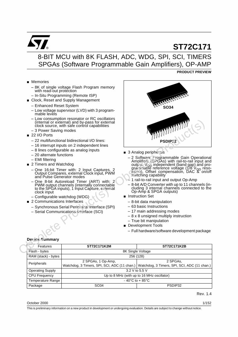
ST72C1718-BIT MCU with 8K FLASH, ADC, WDG, SPI, SCI, TIMERSSPGAs (Software Programmable Gain Amplifiers), OP-AMP
PRODUCT PREVIEW
Memories– 8K of single voltage Flash Program memory
with read-out protection– In-Situ Programming (Remote ISP)
Clock, Reset and Supply Management– Enhanced Reset System– Low voltage supervisor (LVD) with 3 program-
mable levels– Low consumption resonator or RC oscillators
(internal or external) and by-pass for externalclock source, with safe control capabilities
– 3 Power Saving modes 22 I/O Ports
– 22 multifunctional bidirectional I/O lines: – 16 interrupt inputs on 2 independent lines– 8 lines configurable as analog inputs– 20 alternate functions– EMI filtering
2 Timers and Watchdog– One 16-bit Timer with: 2 Input Captures, 2
Output Compares, external Clock input, PWMand Pulse Generator modes
– One 8-bit Autoreload Timer (ART) with: 2PWM output channels (internally connectableto the SPGA inputs), 1 Input Capture, externalclock input
– Configurable watchdog (WDG) 2 Communications Interfaces
– Synchronous Serial Peripheral Interface (SPI)– Serial Communications Interface (SCI)
3 Analog peripherals– 2 Software Programmable Gain Operational
Amplifiers (SPGAs) with rail-to-rail input andoutput, VDD independent (band gap) and pro-grammable reference voltage (1/8 VDD reso-lution), Offset compensation, DAC & on/offswitching capability
– 1 rail-to-rail input and output Op-Amp– 8-bit A/D Converter with up to 11 channels (in-
cluding 3 internal channels connected to theOp-Amp & SPGA outputs)
Instruction Set– 8-bit data manipulation– 63 basic Instructions– 17 main addressing modes– 8 x 8 unsigned multiply instruction– True bit manipulation
Development Tools– Full hardware/software development package
Device Summary
SO34
PSDIP32
Features ST72C171K2M ST72C171K2BFlash - bytes 8K Single Voltage
RAM (stack) - bytes 256 (128)
Peripherals2 SPGAs, 1 Op-Amp,
Watchdog, 3 Timers, SPI, SCI, ADC (11 chan.)2 SPGAs,
Watchdog, 3 Timers, SPI, SCI, ADC (11 chan.)
Operating Supply 3.2 V to 5.5 V
CPU Frequency Up to 8 MHz (with up to 16 MHz oscillator)
Temperature Range - 40°C to + 85°C
Package SO34 PSDIP32
1
Obsolete Product(
s) - O
bsolete Product(
s)
Obsolete Product(
s) - O
bsolete Product(
s)
Table of Contents
152
2/152
1
1 GENERAL DESCRIPTION . . . . . . . . . . . . . . . . . . . . . . . . . . . . . . . . . . . . . . . . . . . . . . . . . . . . . . 41.1 INTRODUCTION . . . . . . . . . . . . . . . . . . . . . . . . . . . . . . . . . . . . . . . . . . . . . . . . . . . . . . . . . 4
1.2 PIN DESCRIPTION . . . . . . . . . . . . . . . . . . . . . . . . . . . . . . . . . . . . . . . . . . . . . . . . . . . . . . . 5
1.3 MEMORY MAP . . . . . . . . . . . . . . . . . . . . . . . . . . . . . . . . . . . . . . . . . . . . . . . . . . . . . . . . . . 8
2 FLASH PROGRAM MEMORY . . . . . . . . . . . . . . . . . . . . . . . . . . . . . . . . . . . . . . . . . . . . . . . . . . 112.1 INTRODUCTION . . . . . . . . . . . . . . . . . . . . . . . . . . . . . . . . . . . . . . . . . . . . . . . . . . . . . . . . 11
2.2 MAIN FEATURES . . . . . . . . . . . . . . . . . . . . . . . . . . . . . . . . . . . . . . . . . . . . . . . . . . . . . . . 11
2.3 STRUCTURAL ORGANISATION . . . . . . . . . . . . . . . . . . . . . . . . . . . . . . . . . . . . . . . . . . . . 11
2.4 IN-SITU PROGRAMMING (ISP) MODE . . . . . . . . . . . . . . . . . . . . . . . . . . . . . . . . . . . . . . 11
2.5 MEMORY READ-OUT PROTECTION . . . . . . . . . . . . . . . . . . . . . . . . . . . . . . . . . . . . . . . . 11
3 CENTRAL PROCESSING UNIT . . . . . . . . . . . . . . . . . . . . . . . . . . . . . . . . . . . . . . . . . . . . . . . . . 123.1 INTRODUCTION . . . . . . . . . . . . . . . . . . . . . . . . . . . . . . . . . . . . . . . . . . . . . . . . . . . . . . . . 12
3.2 MAIN FEATURES . . . . . . . . . . . . . . . . . . . . . . . . . . . . . . . . . . . . . . . . . . . . . . . . . . . . . . . 12
3.3 CPU REGISTERS . . . . . . . . . . . . . . . . . . . . . . . . . . . . . . . . . . . . . . . . . . . . . . . . . . . . . . . 12
4 SUPPLY, RESET AND CLOCK MANAGEMENT . . . . . . . . . . . . . . . . . . . . . . . . . . . . . . . . . . . . 154.1 MAIN FEATURES . . . . . . . . . . . . . . . . . . . . . . . . . . . . . . . . . . . . . . . . . . . . . . . . . . . . . . . 15
4.2 LOW VOLTAGE DETECTOR (LVD) . . . . . . . . . . . . . . . . . . . . . . . . . . . . . . . . . . . . . . . . . 16
4.3 CLOCK SECURITY SYSTEM (CSS) . . . . . . . . . . . . . . . . . . . . . . . . . . . . . . . . . . . . . . . . . 21
4.4 CLOCK, RESET AND SUPPLY REGISTER DESCRIPTION . . . . . . . . . . . . . . . . . . . . . . 23
5 INTERRUPTS . . . . . . . . . . . . . . . . . . . . . . . . . . . . . . . . . . . . . . . . . . . . . . . . . . . . . . . . . . . . . . . 245.1 NON MASKABLE SOFTWARE INTERRUPT . . . . . . . . . . . . . . . . . . . . . . . . . . . . . . . . . . 24
5.2 EXTERNAL INTERRUPTS . . . . . . . . . . . . . . . . . . . . . . . . . . . . . . . . . . . . . . . . . . . . . . . . 24
5.3 PERIPHERAL INTERRUPTS . . . . . . . . . . . . . . . . . . . . . . . . . . . . . . . . . . . . . . . . . . . . . . . 24
6 POWER SAVING MODES . . . . . . . . . . . . . . . . . . . . . . . . . . . . . . . . . . . . . . . . . . . . . . . . . . . . . 276.1 INTRODUCTION . . . . . . . . . . . . . . . . . . . . . . . . . . . . . . . . . . . . . . . . . . . . . . . . . . . . . . . . 27
6.2 SLOW MODE . . . . . . . . . . . . . . . . . . . . . . . . . . . . . . . . . . . . . . . . . . . . . . . . . . . . . . . . . . . 27
6.3 WAIT MODE . . . . . . . . . . . . . . . . . . . . . . . . . . . . . . . . . . . . . . . . . . . . . . . . . . . . . . . . . . . 28
6.4 HALT MODE . . . . . . . . . . . . . . . . . . . . . . . . . . . . . . . . . . . . . . . . . . . . . . . . . . . . . . . . . . . 29
7 ON-CHIP PERIPHERALS . . . . . . . . . . . . . . . . . . . . . . . . . . . . . . . . . . . . . . . . . . . . . . . . . . . . . . 307.1 I/O PORTS . . . . . . . . . . . . . . . . . . . . . . . . . . . . . . . . . . . . . . . . . . . . . . . . . . . . . . . . . . . . . 30
7.2 MISCELLANEOUS REGISTERS . . . . . . . . . . . . . . . . . . . . . . . . . . . . . . . . . . . . . . . . . . . . 36
7.3 OP-AMP MODULE . . . . . . . . . . . . . . . . . . . . . . . . . . . . . . . . . . . . . . . . . . . . . . . . . . . . . . . 38
7.4 WATCHDOG TIMER (WDG) . . . . . . . . . . . . . . . . . . . . . . . . . . . . . . . . . . . . . . . . . . . . . . . 48
7.5 16-BIT TIMER . . . . . . . . . . . . . . . . . . . . . . . . . . . . . . . . . . . . . . . . . . . . . . . . . . . . . . . . . . 51
7.6 PWM AUTO-RELOAD TIMER (ART) . . . . . . . . . . . . . . . . . . . . . . . . . . . . . . . . . . . . . . . . . 69
7.7 SERIAL COMMUNICATIONS INTERFACE (SCI) . . . . . . . . . . . . . . . . . . . . . . . . . . . . . . . 78
7.8 SERIAL PERIPHERAL INTERFACE (SPI) . . . . . . . . . . . . . . . . . . . . . . . . . . . . . . . . . . . . 89
7.9 8-BIT A/D CONVERTER (ADC) . . . . . . . . . . . . . . . . . . . . . . . . . . . . . . . . . . . . . . . . . . . . 102
8 INSTRUCTION SET . . . . . . . . . . . . . . . . . . . . . . . . . . . . . . . . . . . . . . . . . . . . . . . . . . . . . . . . . 1068.1 ST7 ADDRESSING MODES . . . . . . . . . . . . . . . . . . . . . . . . . . . . . . . . . . . . . . . . . . . . . . 106
8.2 INSTRUCTION GROUPS . . . . . . . . . . . . . . . . . . . . . . . . . . . . . . . . . . . . . . . . . . . . . . . . 109
Obsolete Product(
s) - O
bsolete Product(
s)
Table of Contents
3/152
9 ELECTRICAL CHARACTERISTICS . . . . . . . . . . . . . . . . . . . . . . . . . . . . . . . . . . . . . . . . . . . . . 1129.1 PARAMETER CONDITIONS . . . . . . . . . . . . . . . . . . . . . . . . . . . . . . . . . . . . . . . . . . . . . . 112
9.2 ABSOLUTE MAXIMUM RATINGS . . . . . . . . . . . . . . . . . . . . . . . . . . . . . . . . . . . . . . . . . . 113
9.3 OPERATING CONDITIONS . . . . . . . . . . . . . . . . . . . . . . . . . . . . . . . . . . . . . . . . . . . . . . . 114
9.4 SUPPLY CURRENT CHARACTERISTICS . . . . . . . . . . . . . . . . . . . . . . . . . . . . . . . . . . . 116
9.5 CLOCK AND TIMING CHARACTERISTICS . . . . . . . . . . . . . . . . . . . . . . . . . . . . . . . . . . 119
9.6 MEMORY CHARACTERISTICS . . . . . . . . . . . . . . . . . . . . . . . . . . . . . . . . . . . . . . . . . . . 123
9.7 EMC CHARACTERISTICS . . . . . . . . . . . . . . . . . . . . . . . . . . . . . . . . . . . . . . . . . . . . . . . 124
9.8 I/O PORT PIN CHARACTERISTICS . . . . . . . . . . . . . . . . . . . . . . . . . . . . . . . . . . . . . . . . 129
9.9 CONTROL PIN CHARACTERISTICS . . . . . . . . . . . . . . . . . . . . . . . . . . . . . . . . . . . . . . . 132
9.10 TIMER PERIPHERAL CHARACTERISTICS . . . . . . . . . . . . . . . . . . . . . . . . . . . . . . . . . . 135
9.11 COMMUNICATION INTERFACE CHARACTERISTICS . . . . . . . . . . . . . . . . . . . . . . . . . 136
9.12 8-BIT ADC CHARACTERISTICS . . . . . . . . . . . . . . . . . . . . . . . . . . . . . . . . . . . . . . . . . . . 139
9.13 OP-AMP MODULE CHARACTERISTICS . . . . . . . . . . . . . . . . . . . . . . . . . . . . . . . . . . . . 141
10 GENERAL INFORMATION . . . . . . . . . . . . . . . . . . . . . . . . . . . . . . . . . . . . . . . . . . . . . . . . . . . 14410.1 PACKAGE MECHANICAL DATA . . . . . . . . . . . . . . . . . . . . . . . . . . . . . . . . . . . . . . . . . . . 144
10.2 THERMAL CHARACTERISTICS . . . . . . . . . . . . . . . . . . . . . . . . . . . . . . . . . . . . . . . . . . 145
10.3 SOLDERING AND GLUEABILITY INFORMATION . . . . . . . . . . . . . . . . . . . . . . . . . . . . . 146
10.4 PACKAGE/SOCKET FOOTPRINT PROPOSAL . . . . . . . . . . . . . . . . . . . . . . . . . . . . . . . 146
11 DEVICE CONFIGURATION AND ORDERING INFORMATION . . . . . . . . . . . . . . . . . . . . . . . 14711.1 OPTION BYTES . . . . . . . . . . . . . . . . . . . . . . . . . . . . . . . . . . . . . . . . . . . . . . . . . . . . . . . . 147
11.2 DEVICE ORDERING INFORMATION . . . . . . . . . . . . . . . . . . . . . . . . . . . . . . . . . . . . . . . 148
11.3 DEVELOPMENT TOOLS . . . . . . . . . . . . . . . . . . . . . . . . . . . . . . . . . . . . . . . . . . . . . . . . . 149
11.4 ST7 APPLICATION NOTES . . . . . . . . . . . . . . . . . . . . . . . . . . . . . . . . . . . . . . . . . . . . . . 150
11.5 TO GET MORE INFORMATION . . . . . . . . . . . . . . . . . . . . . . . . . . . . . . . . . . . . . . . . . . . 150
12 SUMMARY OF CHANGES . . . . . . . . . . . . . . . . . . . . . . . . . . . . . . . . . . . . . . . . . . . . . . . . . . . 151
Obsolete Product(
s) - O
bsolete Product(
s)
ST72C171
4/152
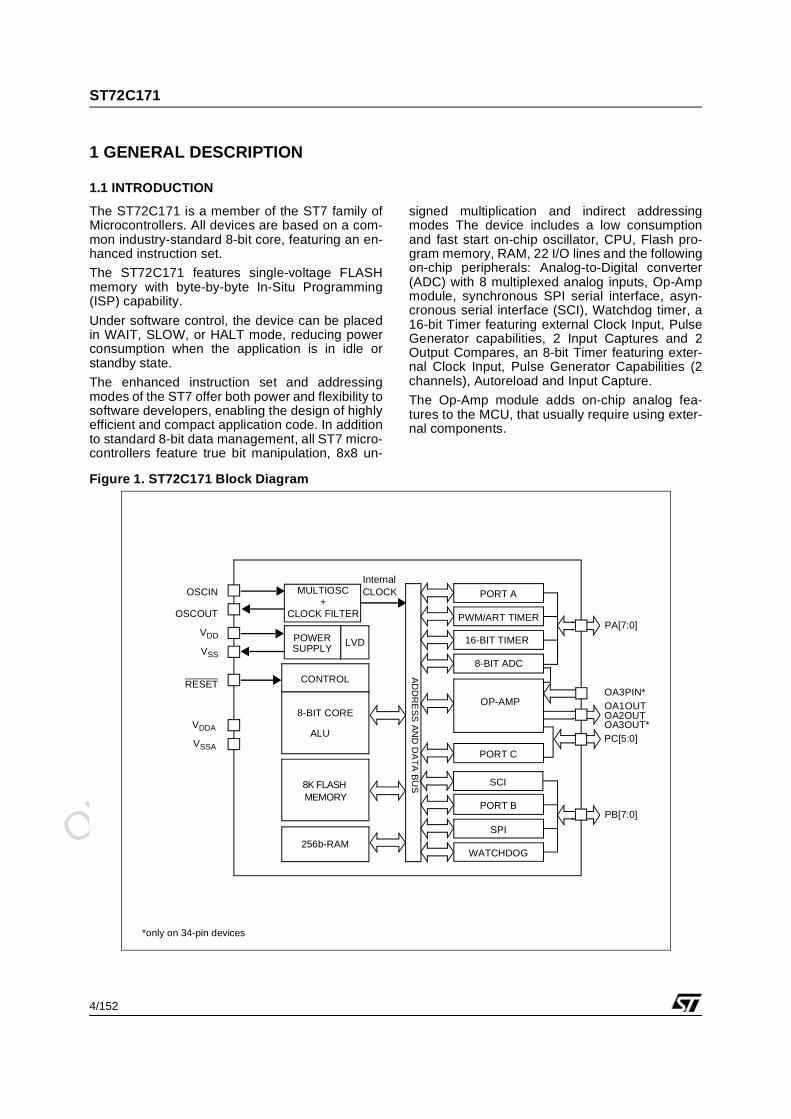
1 GENERAL DESCRIPTION
1.1 INTRODUCTION
The ST72C171 is a member of the ST7 family ofMicrocontrollers. All devices are based on a com-mon industry-standard 8-bit core, featuring an en-hanced instruction set.
The ST72C171 features single-voltage FLASHmemory with byte-by-byte In-Situ Programming(ISP) capability.
Under software control, the device can be placedin WAIT, SLOW, or HALT mode, reducing powerconsumption when the application is in idle orstandby state.
The enhanced instruction set and addressingmodes of the ST7 offer both power and flexibility tosoftware developers, enabling the design of highlyefficient and compact application code. In additionto standard 8-bit data management, all ST7 micro-controllers feature true bit manipulation, 8x8 un-
signed multiplication and indirect addressingmodes The device includes a low consumptionand fast start on-chip oscillator, CPU, Flash pro-gram memory, RAM, 22 I/O lines and the followingon-chip peripherals: Analog-to-Digital converter(ADC) with 8 multiplexed analog inputs, Op-Ampmodule, synchronous SPI serial interface, asyn-cronous serial interface (SCI), Watchdog timer, a16-bit Timer featuring external Clock Input, PulseGenerator capabilities, 2 Input Captures and 2Output Compares, an 8-bit Timer featuring exter-nal Clock Input, Pulse Generator Capabilities (2channels), Autoreload and Input Capture.
The Op-Amp module adds on-chip analog fea-tures to the MCU, that usually require using exter-nal components.
Figure 1. ST72C171 Block Diagram
AD
DR
ES
S A
ND
DA
TA
BU
S
OSCIN
OSCOUT
RESET
16-BIT TIMER
8-BIT ADC
PORT B
WATCHDOG
InternalCLOCK
CONTROL
256b-RAM
PA[7:0]
VSS
VDD POWERSUPPLY
8K FLASH
PORT A
PWM/ART TIMER
SPI
PB[7:0]
LVD
SCI
MULTIOSC+
CLOCK FILTER
OP-AMP
VSSA
VDDA
8-BIT CORE
ALU
PORT C
PC[5:0]
OA1OUTOA2OUT
MEMORY
OA3OUT*
*only on 34-pin devices
OA3PIN*
Obsolete Product(
s) - O
bsolete Product(
s)
ST72C171
5/152
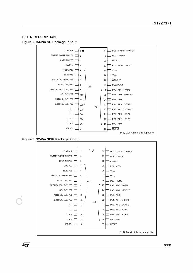
1.2 PIN DESCRIPTION
Figure 2. 34-Pin SO Package Pinout
Figure 3. 32-Pin SDIP Package Pinout
PC2 / OA1PIN / PWM0R
PC3 / OA1NIN
OA1OUT
PC4 / MCO/ OA3NIN
VDDA
VSSA
OA3OUT
PC5/ PWM0
PA7 / AIN7 / PWM1
PA6 / AIN6 / ARTICP0
PA5 / AIN5
PA4 / AIN4 / OCMP1
PA3 / AIN3 / OCMP2
PA2 / AIN2 / ICAP1
PA1 / AIN1 / ICAP2
PA0 / AIN0
RESET
21
22
23
24
25
26
34
33
32
31
30
29
28
27
1
2
3
4
5
6
7
8
9
10
11
12
13
14
OA2OUT
PWM1R / OA2PIN / PC1
OA2NIN / PC0
OA3PIN
TDO / PB7
RDI / PB6
ISPDATA / MISO / PB5
MOSI / (HS) PB4
ISPCLK / SCK / (HS) PB3
SS / (HS) PB2
ARTCLK / (HS) PB1
EXTCLK / (HS) PB0
VDD
VSS
OSC2
OSC1
ISPSEL
15
16
17
20
19
18
ei1
ei0
(HS) 20mA high sink capability
OA2OUT
PWM1R / OA2PIN / PC1
OA2NIN / PC0
TDO / PB7
RDI / PB6
ISPDATA / MISO / PB5
MOSI / (HS) PB4
ISPCLK / SCK/ (HS) PB3
SS / (HS) PB2
ARTCLK / (HS) PB1
EXTCLK / (HS) PB0
VDD
VSS
OSC2
OSC1
ISPSEL
PC2 / OA1PIN / PWM0R
PC3 / OA1NIN
OA1OUT
PC4 / MCO
VDDA
VSSA
PC5 / PWM0
PA7 / AIN7 / PWM1
PA6 / AIN6 /ARTICP0
PA5 / AIN5
PA4 / AIN4 / OCMP1
PA3 / AIN3 / OCMP2
PA2 / AIN2 / ICAP1
PA1 / AIN1 / ICAP2
PA0 / AIN0
RESET
1
2
3
4
5
6
7
8
9
10
11
12
13
14
15
16
32
31
30
29
28
27
26
25
24
23
22
21
20
19
18
17
ei1
ei0
(HS) 20mA high sink capability
Obsolete Product(
s) - O
bsolete Product(
s)
ST72C171
6/152
PIN DESCRIPTION (Cont’d)
Legend / Abbreviations:Type: I = input, O = output, S = supply
In/Output level: C = CMOS 0.3VDD/0.7VDD,CR = CMOS Levels with resistive output (1K)
A = Analog levels
Output level: HS = high sink (on N-buffer only),
Port configuration capabilities:
– Input:float = floating, wpu = weak pull-up, int = interrupt, ana = analog
– Output: OD = open drain, T = true open drain, PP = push-pull
Note: the Reset configuration of each pin is shown in bold.
Table 1. Device Pin Description
Pin n°
Pin Name
Typ
e
Level Port Mainfunction
(afterreset)
Alternate function
SD
IP32
SO
34
Inp
ut
Ou
tpu
t Input Output
flo
at
wp
u
int
ana
OD
PP
1 1 OA2OUT O A OA2 output
2 2PC1/OA2PIN/PWM1R
I/O C C/CR X X X X X Port C1OA2 noninverting input and/or ART PWM1 resistive output
3 3 PC0/OA2NIN I/O C/A C X X X X X Port C0 OA2 inverting input
- 4 OA3PIN I A OA3 noninverting input
4 5 PB7/TDO I/O C X ei1 X X Port B7 SCI transmit
5 6 PB6/RDI I/O C X ei1 X X Port B6 SCI receive
6 7 PB5/MISO/ISPDATA I/O C X ei1 X X Port B5SPI data master in/slave out or In Situ Programming Data In-put
7 8 PB4/MOSI I/O C HS X ei1 X X Port B4 SPI data master out/slave in
8 9 PB3/SCK/ISPCLK I/O C HS X ei1 X X Port B3SPI Clock or In Situ Program-ming Clock Output
9 10 PB2/SS I/O C HS X ei1 X X Port B2 SPI Slave Select (active low)
10 11 PB1/ARTCLK I/O C HS X ei1 X X Port B1 ART External Clock
11 12 PB0/EXTCLK I/O C HS X ei1 X X Port B0 Timer16 External Clock
12 13 VDD S Digital Main Supply Voltage
13 14 VSS S Digital ground voltage
14 15 OSC2 Resonator oscillator inverter output or capaci-tor input for RC oscillator
15 16 OSC1External clock input or Resonator oscillator in-verter input or resistor input for RC oscillator
16 17 ISPSEL I CIn Situ Programming Mode Select
Must be tied to VSS in user mode
17 18 RESET I/O C X X External Reset
18 19 PA0/AIN0 I/O C X ei0 X X X Port A0 ADC input 0
19 20 PA1/AIN1/ICAP2 I/O C X ei0 X X X Port A1ADC input 1 orTimer16 input capture 2
Obsolete Product(
s) - O
bsolete Product(
s)
ST72C171
7/152
Notes:1. In the interrupt input column, “eix” defines the associated external interrupt vector. If the weak pull-upcolumn (wpu) is associated with the interrupt column (int), then the I/O configuration is pull-up interruptinput, else the configuration is floating interrupt input.2. OSC1 and OSC2 pins connect a crystal or ceramic resonator, an external RC, or an external source tothe on-chip oscillator see dedicated See “PIN DESCRIPTION” on page 5. for more details.
20 21 PA2/AIN2/ICAP1 I/O C X ei0 X X X Port A2ADC input 2or Timer16 input capture 1
21 22 PA3/AIN3/OCMP2 I/O C X ei0 X X X Port A3ADC input 3 or Timer16 output compare 2
22 23 PA4 /AIN4/OCMP1 I/O C X ei0 X X X Port A4ADC input 4 or Timer16 output compare 1
23 24 PA5/AIN5 I/O C X ei0 X X X Port A5 ADC input 5
24 25 PA6/AIN6/ARTICP0 I/O C X ei0 X X X Port A6ADC input 6 or ART input cap-ture
25 26 PA7/AIN7/PWM1 I/O C X ei0 X X X Port A7ADC input 7 or ART PWM1 output
26 27 PC5 / PWM0 I/O C X X X X Port C5 ART PWM0 output
- 28 OA3OUT O A OA3 output
27 29 VSSA Analog ground
28 30 VDDA Analog supply
29 31 PC4/MCO/OA3NIN I/O C X X X X Port C4Main Clock Out or OA3 invert-ing input
30 32 OA1OUT O A OA1 output
31 33 PC3/OA1NIN I/O C/A C X X X X Port C3 OA1 inverting input
32 34PC2/OA1PIN/PWM0R
I/O C/A C/CR X X X X Port C2OA1 non-inverting input and/or ART PWM0 resistive output
Pin n°
Pin Name
Typ
e
Level Port Mainfunction
(afterreset)
Alternate function
SD
IP32
SO
34
Inp
ut
Ou
tpu
t Input Output
flo
at
wp
u
int
ana
OD
PP
Obsolete Product(
s) - O
bsolete Product(
s)
ST72C171
8/152
1.3 MEMORY MAP
1.3.1 Introduction
Figure 4. Program Memory Map
Short AddressingRAM
Stack
0100h
017Fh
0080h
00FFh
0000h
8 Kbytes
Interrupt & Reset Vectors
HW Registers
017Fh
0080h
007Fh
0180h
DFFFh
Reserved
(see Table 1.3.2)
E000h
FFDFh
FFE0h
FFFFh(see Table 4)
256 bytes RAM
FLASH
(128 Bytes)
(128 Bytes)
Zero page
Obsolete Product(
s) - O
bsolete Product(
s)
ST72C171
9/152
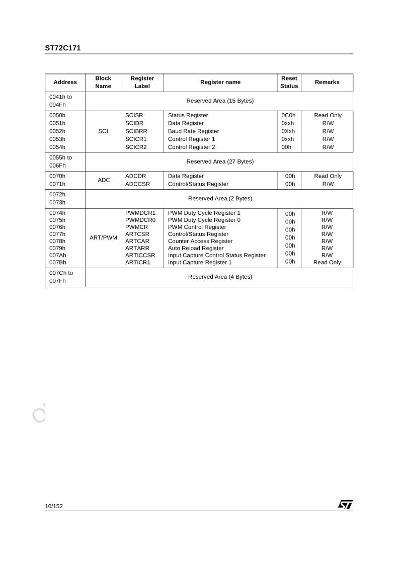
1.3.2 Data Register
Table 2. Hardware Register Memory Map
AddressBlockName
Register Label
Register nameReset Status
Remarks
0000h0001h0002h0003h
Port A
PADRPADDRPAOR
Data RegisterData Direction RegisterOption RegisterNot Used
00h00h00h
R/WR/W R/W
Absent
0004h0005h0006h0007h
Port B
PBDRPBDDRPBOR
Data RegisterData Direction RegisterOption RegisterNot Used
00h00h00h
R/W R/W R/W
Absent
0008h0009h000Ah
Port CPCDRPCDDRPCOR
Data RegisterData Direction RegisterOption Register
00h00h00h
R/W R/W R/W
000Bh to001Ah
Reserved Area (16 Bytes)
001Bh001Ch001Dh001Eh001Fh
OPAMP
OA1CROA2CROA3CROAIRR
OAVRCR
OA1 Control RegisterOA2 Control RegisterOA3 Control RegisterOA Interrupt & Readout RegisterOA Voltage Reference Control Register
00h00h00h00h00h
R/W R/W R/W
Section 7.3R/W
0020h MISC1 MISCR1 Miscellaneous Register 1 00h see Section 4.3.5
0021h0022h0023h
SPISPIDRSPICRSPISR
Data I/O RegisterControl RegisterStatus Register
xxh0xh00h
R/W R/W
Read Only
0024h WDG WDGCR Watchdog Control register 7Fh R/W
0025h CRS CRSRClock, Reset and Supply Control / Status Register
00h R/W
0026h to0030h
Reserved Area (11 Bytes)
0031h0032h0033h0034h-0035h0036h-0037h0038h-0039h003Ah-003Bh003Ch-003Dh003Eh-003Fh
TIMER16
TACR2TACR1TASRTAIC1HRTAIC1LRTAOC1HRTAOC1LRTACHRTACLRTAACHRTAACLRTAIC2HRTAIC2LRTAOC2HRTAOC2LR
Control Register2Control Register1Status RegisterInput Capture1 High RegisterInput Capture1 Low RegisterOutput Compare1 High RegisterOutput Compare1 Low RegisterCounter High RegisterCounter Low RegisterAlternate Counter High RegisterAlternate Counter Low RegisterInput Capture2 High RegisterInput Capture2 Low RegisterOutput Compare2 High RegisterOutput Compare2 Low Register
00h00hxxhxxhxxh80h00hFFhFChFFhFChxxhxxh80h00h
R/W R/W
Read Only Read Only Read Only
R/W R/W
Read Only Read Only Read Only Read Only Read Only Read Only
R/W R/W
0040h MISC2 MISCR2 Miscellaneous Register2 00h see Section 7.2.2
Obsolete Product(
s) - O
bsolete Product(
s)
ST72C171
10/152
0041h to004Fh
Reserved Area (15 Bytes)
0050h0051h0052h0053h0054h
SCI
SCISRSCIDRSCIBRRSCICR1SCICR2
Status RegisterData RegisterBaud Rate RegisterControl Register 1Control Register 2
0C0h0xxh0Xxh0xxh00h
Read Only R/W R/W R/W R/W
0055h to006Fh
Reserved Area (27 Bytes)
0070h0071h
ADCADCDRADCCSR
Data RegisterControl/Status Register
00h00h
Read Only R/W
0072h0073h
Reserved Area (2 Bytes)
0074h0075h0076h0077h0078h0079h007Ah007Bh
ART/PWM
PWMDCR1PWMDCR0PWMCRARTCSRARTCARARTARRARTICCSRARTICR1
PWM Duty Cycle Register 1PWM Duty Cycle Register 0PWM Control RegisterControl/Status RegisterCounter Access RegisterAuto Reload RegisterInput Capture Control Status RegisterInput Capture Register 1
00h00h00h00h00h00h00h
R/W R/W R/W R/W R/W R/W R/W
Read Only
007Ch to007Fh
Reserved Area (4 Bytes)
AddressBlockName
Register Label
Register nameReset Status
Remarks
Obsolete Product(
s) - O
bsolete Product(
s)
ST72C171
11/152
2 FLASH PROGRAM MEMORY
2.1 INTRODUCTION
FLASH devices have a single voltage non-volatileFLASH memory that may be programmed in-situ(or plugged in a programming tool) on a byte-by-byte basis.
2.2 MAIN FEATURES
Remote In-Situ Programming (ISP) mode Up to 16 bytes programmed in the same cycle MTP memory (Multiple Time Programmable) Read-out memory protection against piracy
2.3 STRUCTURAL ORGANISATION
The FLASH program memory is organised in asingle 8-bit wide memory block which can be usedfor storing both code and data constants.
The FLASH program memory is mapped in the up-per part of the ST7 addressing space and includesthe reset and interrupt user vector area .
2.4 IN-SITU PROGRAMMING (ISP) MODE
The FLASH program memory can be programmedusing Remote ISP mode. This ISP mode allowsthe contents of the ST7 program memory to be up-dated using a standard ST7 programming tools af-ter the device is mounted on the application board.This feature can be implemented with a minimumnumber of added components and board area im-pact.
An example Remote ISP hardware interface to thestandard ST7 programming tool is described be-low. For more details on ISP programming, refer tothe ST7 Programming Specification.
Remote ISP OverviewThe Remote ISP mode is initiated by a specific se-quence on the dedicated ISPSEL pin.
The Remote ISP is performed in three steps:
– Selection of the RAM execution mode
– Download of Remote ISP code in RAM
– Execution of Remote ISP code in RAM to pro-gram the user program into the FLASH
Remote ISP hardware configurationIn Remote ISP mode, the ST7 has to be suppliedwith power (VDD and VSS) and a clock signal (os-cillator and application crystal circuit for example).
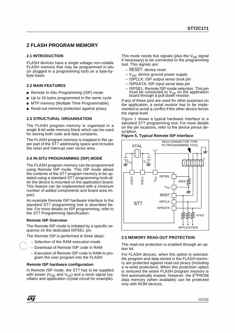
This mode needs five signals (plus the VDD signalif necessary) to be connected to the programmingtool. This signals are:
– RESET: device reset– VSS: device ground power supply– ISPCLK: ISP output serial clock pin– ISPDATA: ISP input serial data pin– ISPSEL: Remote ISP mode selection. This pin
must be connected to VSS on the applicationboard through a pull-down resistor.
If any of these pins are used for other purposes onthe application, a serial resistor has to be imple-mented to avoid a conflict if the other device forcesthe signal level.
Figure 1 shows a typical hardware interface to astandard ST7 programming tool. For more detailson the pin locations, refer to the device pinout de-scription.Figure 5. Typical Remote ISP Interface
2.5 MEMORY READ-OUT PROTECTION
The read-out protection is enabled through an op-tion bit.
For FLASH devices, when this option is selected,the program and data stored in the FLASH memo-ry are protected against read-out piracy (includinga re-write protection). When this protection optionis removed the entire FLASH program memory isfirst automatically erased. However, the E2PROMdata memory (when available) can be protectedonly with ROM devices.
ISPSEL
VSS
RESET
ISPCLK
ISPDATA
OS
C1
OS
C2
VD
D
ST7
HE10 CONNECTOR TYPETO PROGRAMMING TOOL
10KΩ
CL0 CL1
APPLICATION
47KΩ
1
XTAL
Obsolete Product(
s) - O
bsolete Product(
s)
ST72C171
12/152
3 CENTRAL PROCESSING UNIT
3.1 INTRODUCTION
This CPU has a full 8-bit architecture and containssix internal registers allowing efficient 8-bit datamanipulation.
3.2 MAIN FEATURES
63 basic instructions Fast 8-bit by 8-bit multiply 17 main addressing modes Two 8-bit index registers 16-bit stack pointer Low power modes Maskable hardware interrupts Non-maskable software interrupt
3.3 CPU REGISTERS
The 6 CPU registers shown in Figure 1 are notpresent in the memory mapping and are accessedby specific instructions.
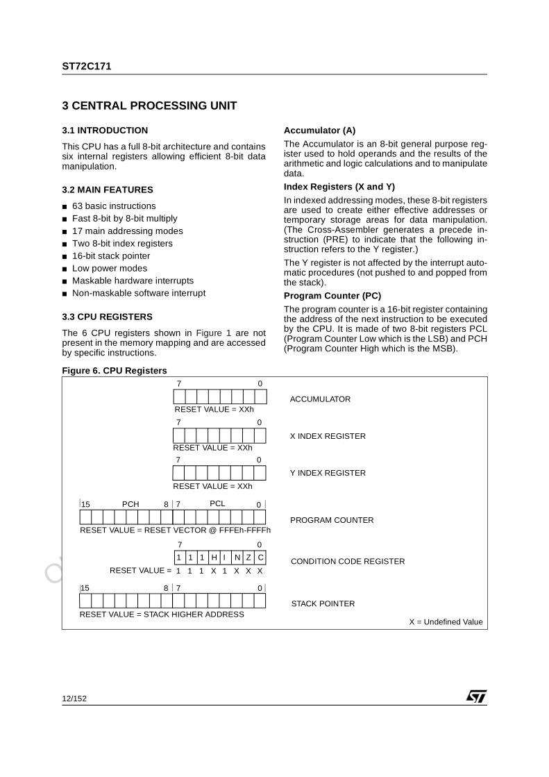
Accumulator (A)
The Accumulator is an 8-bit general purpose reg-ister used to hold operands and the results of thearithmetic and logic calculations and to manipulatedata.
Index Registers (X and Y)
In indexed addressing modes, these 8-bit registersare used to create either effective addresses ortemporary storage areas for data manipulation.(The Cross-Assembler generates a precede in-struction (PRE) to indicate that the following in-struction refers to the Y register.)
The Y register is not affected by the interrupt auto-matic procedures (not pushed to and popped fromthe stack).
Program Counter (PC)
The program counter is a 16-bit register containingthe address of the next instruction to be executedby the CPU. It is made of two 8-bit registers PCL(Program Counter Low which is the LSB) and PCH(Program Counter High which is the MSB).
Figure 6. CPU Registers
ACCUMULATOR
X INDEX REGISTER
Y INDEX REGISTER
STACK POINTER
CONDITION CODE REGISTER
PROGRAM COUNTER
7 0
1 C1 1 H I N Z
RESET VALUE = RESET VECTOR @ FFFEh-FFFFh
7 0
7 0
7 0
0715 8PCH PCL
15 8 7 0
RESET VALUE = STACK HIGHER ADDRESS
RESET VALUE = 1 X1 1 X 1 X X
RESET VALUE = XXh
RESET VALUE = XXh
RESET VALUE = XXh
X = Undefined Value
Obsolete Product(
s) - O
bsolete Product(
s)
ST72C171
13/152
CPU REGISTERS (Cont’d)
CONDITION CODE REGISTER (CC)
Read/Write
Reset Value: 111x1xxx
The 8-bit Condition Code register contains the in-terrupt mask and four flags representative of theresult of the instruction just executed. This registercan also be handled by the PUSH and POP in-structions.
These bits can be individually tested and/or con-trolled by specific instructions.
Bit 4 = H Half carry.
This bit is set by hardware when a carry occurs be-tween bits 3 and 4 of the ALU during an ADD orADC instruction. It is reset by hardware during thesame instructions.0: No half carry has occurred.1: A half carry has occurred.
This bit is tested using the JRH or JRNH instruc-tion. The H bit is useful in BCD arithmetic subrou-tines.
Bit 3 = I Interrupt mask.
This bit is set by hardware when entering in inter-rupt or by software to disable all interrupts exceptthe TRAP software interrupt. This bit is cleared bysoftware.0: Interrupts are enabled.1: Interrupts are disabled.
This bit is controlled by the RIM, SIM and IRET in-structions and is tested by the JRM and JRNM in-structions.
Note: Interrupts requested while I is set arelatched and can be processed when I is cleared.By default an interrupt routine is not interruptable
because the I bit is set by hardware at the start ofthe routine and reset by the IRET instruction at theend of the routine. If the I bit is cleared by softwarein the interrupt routine, pending interrupts areserviced regardless of the priority level of the cur-rent interrupt routine.
Bit 2 = N Negative.
This bit is set and cleared by hardware. It is repre-sentative of the result sign of the last arithmetic,logical or data manipulation. It is a copy of the 7th
bit of the result.0: The result of the last operation is positive or null.1: The result of the last operation is negative
(i.e. the most significant bit is a logic 1).
This bit is accessed by the JRMI and JRPL instruc-tions.
Bit 1 = Z Zero.
This bit is set and cleared by hardware. This bit in-dicates that the result of the last arithmetic, logicalor data manipulation is zero.0: The result of the last operation is different from
zero.1: The result of the last operation is zero.
This bit is accessed by the JREQ and JRNE testinstructions.
Bit 0 = C Carry/borrow.This bit is set and cleared by hardware and soft-ware. It indicates an overflow or an underflow hasoccurred during the last arithmetic operation.0: No overflow or underflow has occurred.1: An overflow or underflow has occurred.
This bit is driven by the SCF and RCF instructionsand tested by the JRC and JRNC instructions. It isalso affected by the “bit test and branch”, shift androtate instructions.
7 0
1 1 1 H I N Z C
Obsolete Product(
s) - O
bsolete Product(
s)
ST72C171
14/152
CENTRAL PROCESSING UNIT (Cont’d)
Stack Pointer (SP)Read/Write
Reset Value: 01 7Fh
The Stack Pointer is a 16-bit register which is al-ways pointing to the next free location in the stack.It is then decremented after data has been pushedonto the stack and incremented before data ispopped from the stack (see Figure 7).
Since the stack is 128 bytes deep, the 10 most sig-nificant bits are forced by hardware. Following anMCU Reset, or after a Reset Stack Pointer instruc-tion (RSP), the Stack Pointer contains its reset val-ue (the SP5 to SP0 bits are set) which is the stackhigher address.
The least significant byte of the Stack Pointer(called S) can be directly accessed by a LD in-struction.
Note: When the lower limit is exceeded, the StackPointer wraps around to the stack upper limit, with-out indicating the stack overflow. The previouslystored information is then overwritten and there-fore lost. The stack also wraps in case of an under-flow.
The stack is used to save the return address dur-ing a subroutine call and the CPU context duringan interrupt. The user may also directly manipulatethe stack by means of the PUSH and POP instruc-tions. In the case of an interrupt, the PCL is storedat the first location pointed to by the SP. Then theother registers are stored in the next locations asshown in Figure 7.
– When an interrupt is received, the SP is decre-mented and the context is pushed on the stack.
– On return from interrupt, the SP is incremented and the context is popped from the stack.
A subroutine call occupies two locations and an in-terrupt five locations in the stack area.
Figure 7. Stack Manipulation Example
15 8
0 0 0 0 0 0 0 1
7 0
0 1 SP5 SP4 SP3 SP2 SP1 SP0
PCH
PCL
SP
PCH
PCL
SP
PCL
PCH
X
ACC
PCH
PCL
SP
PCL
PCH
X
ACC
PCH
PCL
SP
PCL
PCH
X
ACC
PCH
PCL
SP
SP
Y
CALLSubroutine
Interrupt Event
PUSH Y POP Y IRET RETor RSP
@ 017Fh
@ 0100h
Stack Higher Address = 017FhStack Lower Address = 0100h
Obsolete Product(
s) - O
bsolete Product(
s)
ST72C171
15/152
4 SUPPLY, RESET AND CLOCK MANAGEMENTThe device includes a range of utility features forsecuring the application in critical situations (forexample in case of a power brown-out), and re-ducing the number of external components. Anoverview is shown in Figure 8.
4.1 Main Features
Supply Manager– Main supply Low voltage detection (LVD)
– Global power down Reset Sequence Manager (RSM) Multi-Oscillator (MO)
– 4 Crystal/Ceramic resonator oscillators– 2 External RC oscillators– 1 Internal RC oscillator
Clock Security System (CSS)– Clock Filter– Backup Safe Oscillator
Main Clock controller (MCC)
Figure 8. Clock, Reset and Supply Block Diagram
IE SOD0- - - RF RF
CRSR
CSS- WDG
fOSC MAIN CLOCK
CONTROLLER
(MCC)
CF INTERRUPT
LVDLOW VOLTAGE
DETECTOR
(LVD)
MULTI-
OSCILLATOR
(MO)
fCPU
FROMWATCHDOGPERIPHERAL
MCO
OSCOUT
OSCIN
RESET
VDD
VSS
RESET SEQUENCE
MANAGER
(RSM)
CLOCK
FILTER
SAFE
OSC
CLOCK SECURITY SYSTEM(CSS)
Obsolete Product(
s) - O
bsolete Product(
s)
ST72C171
16/152
4.2 LOW VOLTAGE DETECTOR (LVD)
To allow the integration of power managementfeatures in the application, the Low Voltage Detec-tor function (LVD) generates a static reset whenthe VDD supply voltage is below a VIT- referencevalue. This means that it secures the power-up aswell as the power-down keeping the ST7 in reset.
The VIT- reference value for a voltage drop is lowerthan the VIT+ reference value for power-on in orderto avoid a parasitic reset when the MCU starts run-ning and sinks current on the supply (hysteresis).
The LVD Reset circuitry generates a reset whenVDD is below:
– VIT+ when VDD is rising – VIT- when VDD is falling
The LVD function is illustrated in the Figure .
Provided the minimum VDD value (guaranteed forthe oscillator frequency) is above VIT-, the MCUcan only be in two modes:
– under full software control– in static safe reset
In these conditions, secure operation is always en-sured for the application without the need for ex-ternal reset hardware.
During a Low Voltage Detector Reset, the RESETpin is held low, thus permitting the MCU to resetother devices.Notes:1. The LVD allows the device to be used withoutany external RESET circuitry.2. Three different reference levels are selectablethrough the option byte according to the applica-tion requirement.
LVD application note
Application software can detect a reset caused bythe LVD by reading the LVDRF bit in the CRSRregister.
This bit is set by hardware when a LVD reset isgenerated and cleared by software (writing zero).
Figure 9. Low Voltage Detector vs Reset
VDD
VIT+
RESET
VIT-
Vhyst
Obsolete Product(
s) - O
bsolete Product(
s)
ST72C171
17/152
4.2.1 Reset Sequence Manager (RSM)
The RSM block of the CROSS Module includesthree RESET sources as shown in Figure 10: EXTERNAL RESET SOURCE pulse Internal LVD RESET (Low Voltage Detection) Internal WATCHDOG RESET
These sources act on the RESET PIN and it is al-ways kept low during the READ OPTION RESETphase.
The RESET service routine vector is fixed at theFFFEh-FFFFh addresses in the ST7 memorymap.
Figure 10. Reset Block Diagram
The basic RESET sequence consists of 4 phasesas shown in Figure 11: OPTION BYTE reading to configure the device Delay depending on the RESET source 4096 cpu clock cycle delay RESET vector fetch
The duration of the OPTION BYTE reading phase(tROB) is defined in the Electrical Characteristicssection. This first phase is initiated by an externalRESET pin pulse detection, a Watchdog RESETdetection, or when VDD rises up to VLVDopt.
The 4096 cpu clock cycle delay allows the oscilla-tor to stabilise and to ensure that recovery has tak-en place from the Reset state.
The RESET vector fetch phase duration is 2 clockcycles.
Figure 11. RESET Sequence Phases
fCPU
CO
UN
TE
R
RESET
RON
VDD
WATCHDOG RESET
LVD RESET
INTERNALRESET
READ OPTION RESET
RESET
READOPTION BYTE
INTERNAL RESET4096 CLOCK CYCLES
FETCHVECTORDELAY
tROB
Obsolete Product(
s) - O
bsolete Product(
s)
ST72C171
18/152
RESET SEQUENCE MANAGER (Cont’d)
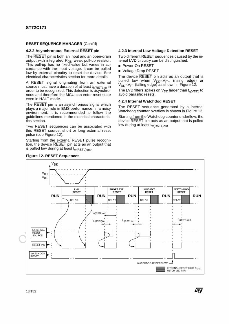
4.2.2 Asynchronous External RESET pin
The RESET pin is both an input and an open-drainoutput with integrated RON weak pull-up resistor.This pull-up has no fixed value but varies in ac-cordance with the input voltage. It can be pulledlow by external circuitry to reset the device. Seeelectrical characteristics section for more details.
A RESET signal originating from an externalsource must have a duration of at least th(RSTL)in inorder to be recognized. This detection is asynchro-nous and therefore the MCU can enter reset stateeven in HALT mode.
The RESET pin is an asynchronous signal whichplays a major role in EMS performance. In a noisyenvironment, it is recommended to follow theguidelines mentioned in the electrical characteris-tics section.
Two RESET sequences can be associated withthis RESET source: short or long external resetpulse (see Figure 12).
Starting from the external RESET pulse recogni-tion, the device RESET pin acts as an output thatis pulled low during at least tw(RSTL)out.
4.2.3 Internal Low Voltage Detection RESET
Two different RESET sequences caused by the in-ternal LVD circuitry can be distinguished: Power-On RESET Voltage Drop RESET
The device RESET pin acts as an output that ispulled low when VDD<VIT+ (rising edge) orVDD<VIT- (falling edge) as shown in Figure 12.
The LVD filters spikes on VDD larger than tg(VDD) toavoid parasitic resets.
4.2.4 Internal Watchdog RESETThe RESET sequence generated by a internalWatchdog counter overflow is shown in Figure 12.
Starting from the Watchdog counter underflow, thedevice RESET pin acts as an output that is pulledlow during at least tw(RSTL)out.
Figure 12. RESET Sequences
VDD
RUN
RESET PIN
EXTERNAL
WATCHDOG
DELAY
VIT+VIT-
th(RSTL)in
tw(RSTL)out
RUNDELAY
th(RSTL)in
DELAY
WATCHDOG UNDERFLOW
tw(RSTL)out
RUN RUNDELAY
RUN
RESET
RESETSOURCE
SHORT EXT.RESET
LVDRESET
LONG EXT.RESET
WATCHDOGRESET
INTERNAL RESET (4096 TCPU)FETCH VECTOR
Obsolete Product(
s) - O
bsolete Product(
s)
ST72C171
19/152
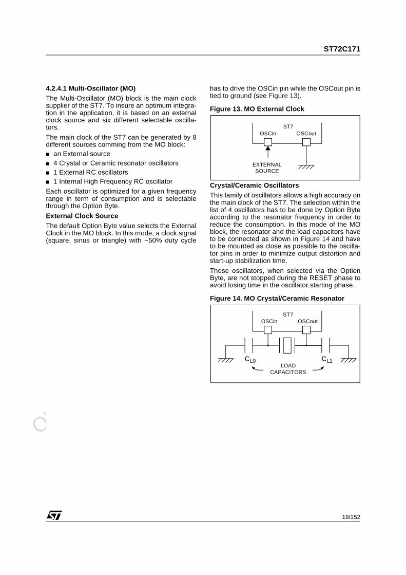
4.2.4.1 Multi-Oscillator (MO)The Multi-Oscillator (MO) block is the main clocksupplier of the ST7. To insure an optimum integra-tion in the application, it is based on an externalclock source and six different selectable oscilla-tors.
The main clock of the ST7 can be generated by 8different sources comming from the MO block: an External source 4 Crystal or Ceramic resonator oscillators 1 External RC oscillators 1 Internal High Frequency RC oscillator
Each oscillator is optimized for a given frequencyrange in term of consumption and is selectablethrough the Option Byte.
External Clock SourceThe default Option Byte value selects the ExternalClock in the MO block. In this mode, a clock signal(square, sinus or triangle) with ~50% duty cycle
has to drive the OSCin pin while the OSCout pin istied to ground (see Figure 13).
Figure 13. MO External Clock
Crystal/Ceramic OscillatorsThis family of oscillators allows a high accuracy onthe main clock of the ST7. The selection within thelist of 4 oscillators has to be done by Option Byteaccording to the resonator frequency in order toreduce the consumption. In this mode of the MOblock, the resonator and the load capacitors haveto be connected as shown in Figure 14 and haveto be mounted as close as possible to the oscilla-tor pins in order to minimize output distortion andstart-up stabilization time.
These oscillators, when selected via the OptionByte, are not stopped during the RESET phase toavoid losing time in the oscillator starting phase.
Figure 14. MO Crystal/Ceramic Resonator
OSCin OSCout
EXTERNAL
ST7
SOURCE
OSCin OSCout
LOADCAPACITORS
ST7
CL1CL0
Obsolete Product(
s) - O
bsolete Product(
s)
ST72C171
20/152
MULTIOSCILLATOR (MO) (Cont’d)
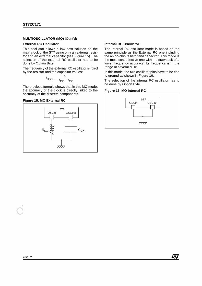
External RC OscillatorThis oscillator allows a low cost solution on themain clock of the ST7 using only an external resis-tor and an external capacitor (see Figure 15). Theselection of the external RC oscillator has to bedone by Option Byte.
The frequency of the external RC oscillator is fixedby the resistor and the capacitor values:
The previous formula shows that in this MO mode,the accuracy of the clock is directly linked to theaccuracy of the discrete components.
Figure 15. MO External RC
Internal RC OscillatorThe Internal RC oscillator mode is based on thesame principle as the External RC one includingthe an on-chip resistor and capacitor. This mode isthe most cost effective one with the drawback of alower frequency accuracy. Its frequency is in therange of several MHz.
In this mode, the two oscillator pins have to be tiedto ground as shown in Figure 16.
The selection of the internal RC oscillator has tobe done by Option Byte.
Figure 16. MO Internal RC
fOSC ~ NREX . CEX
OSCin OSCoutST7
CEXREX
OSCin OSCoutST7
Obsolete Product(
s) - O
bsolete Product(
s)
ST72C171
21/152
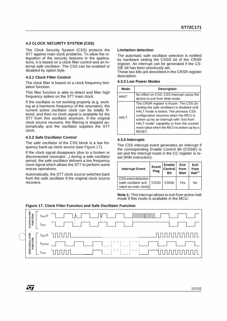
4.3 CLOCK SECURITY SYSTEM (CSS)
The Clock Security System (CSS) protects theST7 against main clock problems. To allow the in-tegration of the security features in the applica-tions, it is based on a clock filter control and an In-ternal safe oscillator. The CSS can be enabled ordisabled by option byte.
4.3.1 Clock Filter ControlThe clock filter is based on a clock frequency limi-tation function.
This filter function is able to detect and filter highfrequency spikes on the ST7 main clock.
If the oscillator is not working properly (e.g. work-ing at a harmonic frequency of the resonator), thecurrent active oscillator clock can be totally fil-tered, and then no clock signal is available for theST7 from this oscillator anymore. If the originalclock source recovers, the filtering is stopped au-tomatically and the oscillator supplies the ST7clock.
4.3.2 Safe Oscillator ControlThe safe oscillator of the CSS block is a low fre-quency back-up clock source (see Figure 17).
If the clock signal disappears (due to a broken ordisconnected resonator...) during a safe oscillatorperiod, the safe oscillator delivers a low frequencyclock signal which allows the ST7 to perform somerescue operations.
Automatically, the ST7 clock source switches backfrom the safe oscillator if the original clock sourcerecovers.
Limitation detection
The automatic safe oscillator selection is notifiedby hardware setting the CSSD bit of the CRSRregister. An interrupt can be generated if the CS-SIE bit has been previously set.These two bits are described in the CRSR registerdescription.
4.3.3 Low Power Modes
4.3.4 InterruptsThe CSS interrupt event generates an interrupt ifthe corresponding Enable Control Bit (CSSIE) isset and the interrupt mask in the CC register is re-set (RIM instruction).
Note 1: This interrupt allows to exit from active-haltmode if this mode is available in the MCU.
Figure 17. Clock Filter Function and Safe Oscillator Function
Mode Description
WAITNo effect on CSS. CSS interrupt cause the device to exit from Wait mode.
HALT
The CRSR register is frozen. The CSS (in-cluding the safe oscillator) is disabled until HALT mode is exited. The previous CSS configuration resumes when the MCU is woken up by an interrupt with “exit from HALT mode” capability or from the counter reset value when the MCU is woken up by a RESET.
Interrupt EventEventFlag
Enable Control
Bit
Exit fromWait
Exit from Halt1)
CSS event detection (safe oscillator acti-vated as main clock)
CSSD CSSIE Yes No
fOSC/2
fCPU
fOSC/2
fCPU
fSFOSC
SA
FE
OS
CIL
LA
TO
RF
UN
CT
ION
CL
OC
KF
ILT
ER
FU
NC
TIO
N
Obsolete Product(
s) - O
bsolete Product(
s)
ST72C171
22/152
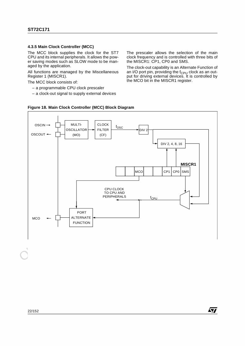
4.3.5 Main Clock Controller (MCC)
The MCC block supplies the clock for the ST7CPU and its internal peripherals. It allows the pow-er saving modes such as SLOW mode to be man-aged by the application.
All functions are managed by the MiscellaneousRegister 1 (MISCR1).
The MCC block consists of:– a programmable CPU clock prescaler– a clock-out signal to supply external devices
The prescaler allows the selection of the mainclock frequency and is controlled with three bits ofthe MISCR1: CP1, CP0 and SMS.
The clock-out capability is an Alternate Function ofan I/O port pin, providing the fCPU clock as an out-put for driving external devices. It is controlled bythe MCO bit in the MISCR1 register.
Figure 18. Main Clock Controller (MCC) Block Diagram
DIV 2, 4, 8, 16
DIV 2
SMSCP1 CP0
CPU CLOCK
MISCR1
TO CPU ANDPERIPHERALS
fOSC
MCO
PORT
FUNCTION
ALTERNATE
OSCOUT
OSCIN MULTI-
OSCILLATOR
(MO)
CLOCK
FILTER
(CF)
MCO
fCPU
Obsolete Product(
s) - O
bsolete Product(
s)
ST72C171
23/152
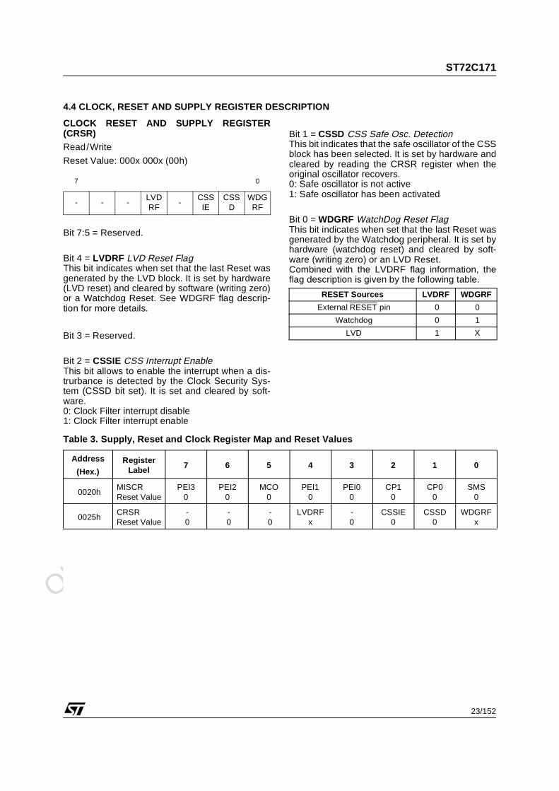
4.4 CLOCK, RESET AND SUPPLY REGISTER DESCRIPTION
CLOCK RESET AND SUPPLY REGISTER(CRSR)Read/Write
Reset Value: 000x 000x (00h)
Bit 7:5 = Reserved.
Bit 4 = LVDRF LVD Reset FlagThis bit indicates when set that the last Reset wasgenerated by the LVD block. It is set by hardware(LVD reset) and cleared by software (writing zero)or a Watchdog Reset. See WDGRF flag descrip-tion for more details.
Bit 3 = Reserved.
Bit 2 = CSSIE CSS Interrupt EnableThis bit allows to enable the interrupt when a dis-trurbance is detected by the Clock Security Sys-tem (CSSD bit set). It is set and cleared by soft-ware.0: Clock Filter interrupt disable1: Clock Filter interrupt enable
Bit 1 = CSSD CSS Safe Osc. DetectionThis bit indicates that the safe oscillator of the CSSblock has been selected. It is set by hardware andcleared by reading the CRSR register when theoriginal oscillator recovers.0: Safe oscillator is not active1: Safe oscillator has been activated
Bit 0 = WDGRF WatchDog Reset FlagThis bit indicates when set that the last Reset wasgenerated by the Watchdog peripheral. It is set byhardware (watchdog reset) and cleared by soft-ware (writing zero) or an LVD Reset.Combined with the LVDRF flag information, theflag description is given by the following table.
Table 3. Supply, Reset and Clock Register Map and Reset Values
7 0
- - -LVDRF
-CSS
IECSS
DWDG
RF
RESET Sources LVDRF WDGRF
External RESET pin 0 0
Watchdog 0 1
LVD 1 X
Address
(Hex.)Register
Label7 6 5 4 3 2 1 0
0020hMISCRReset Value
PEI30
PEI20
MCO0
PEI10
PEI00
CP10
CP00
SMS0
0025hCRSRReset Value
-0
-0
-0
LVDRFx
-0
CSSIE0
CSSD0
WDGRFx
Obsolete Product(
s) - O
bsolete Product(
s)
ST72C171
24/152
5 INTERRUPTSThe ST7 core may be interrupted by one of two dif-ferent methods: maskable hardware interrupts aslisted in the Interrupt Mapping Table and a non-maskable software interrupt (TRAP). The Interruptprocessing flowchart is shown in Figure 19.The maskable interrupts must be enabled clearingthe I bit in order to be serviced. However, disabledinterrupts may be latched and processed whenthey are enabled (see external interrupts subsec-tion).
When an interrupt has to be serviced:
– Normal processing is suspended at the end of the current instruction execution.
– The PC, X, A and CC registers are saved onto the stack.
– The I bit of the CC register is set to prevent addi-tional interrupts.
– The PC is then loaded with the interrupt vector of the interrupt to service and the first instruction of the interrupt service routine is fetched (refer to the Interrupt Mapping Table for vector address-es).
The interrupt service routine should finish with theIRET instruction which causes the contents of thesaved registers to be recovered from the stack.
Note: As a consequence of the IRET instruction,the I bit will be cleared and the main program willresume.
Priority ManagementBy default, a servicing interrupt cannot be inter-rupted because the I bit is set by hardware enter-ing in interrupt routine.
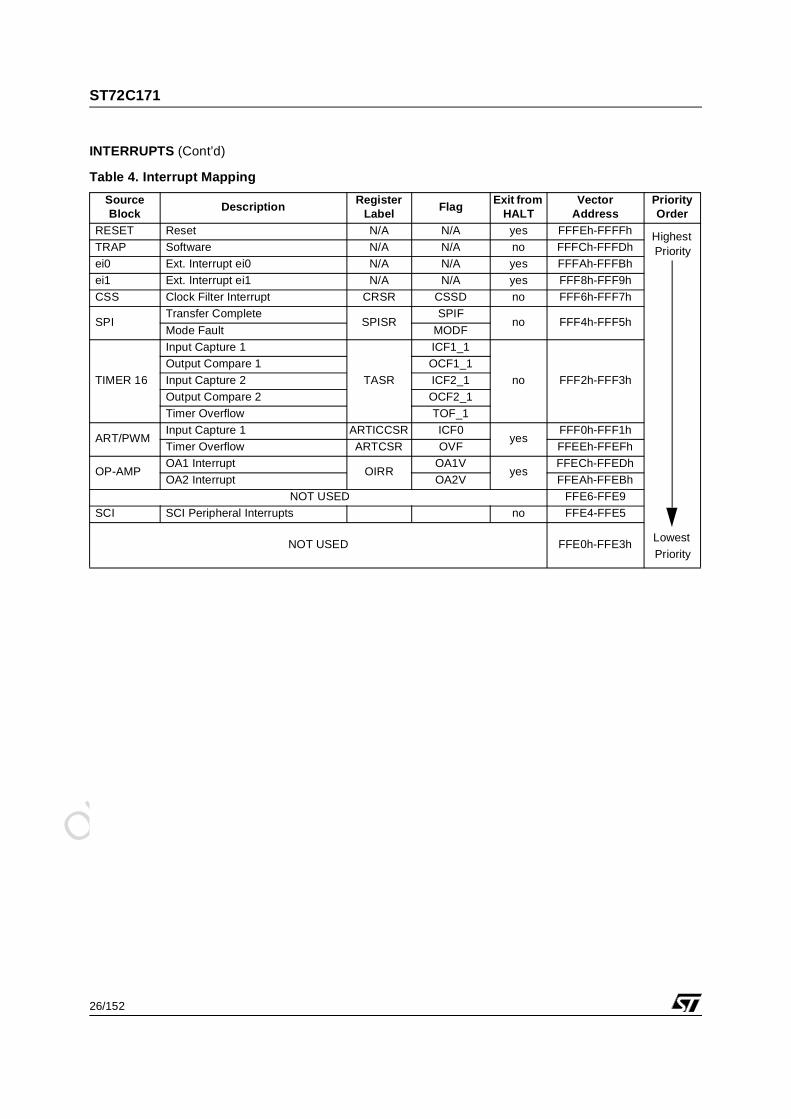
In the case when several interrupts are simultane-ously pending, an hardware priority defines whichone will be serviced first (see the Interrupt Map-ping Table).
Interrupts and Low Power Mode
All interrupts allow the processor to leave theWAIT low power mode. Only external and specifi-cally mentioned interrupts allow the processor toleave the HALT low power mode (refer to the “Exitfrom HALT“ column in the Interrupt Mapping Ta-ble).
5.1 NON MASKABLE SOFTWARE INTERRUPT
This interrupt is entered when the TRAP instruc-tion is executed regardless of the state of the I bit.
It will be serviced according to the flowchart onFigure 19.
5.2 EXTERNAL INTERRUPTS
External interrupt vectors can be loaded into thePC register if the corresponding external interruptoccurred and if the I bit is cleared. These interruptsallow the processor to leave the Halt low powermode.
The external interrupt polarity is selected throughthe miscellaneous register or interrupt register (ifavailable).
An external interrupt triggered on edge will belatched and the interrupt request automaticallycleared upon entering the interrupt service routine.
If several input pins, connected to the same inter-rupt vector, are configured as interrupts, their sig-nals are logically ANDed before entering the edge/level detection block.
Caution: The type of sensitivity defined in the Mis-cellaneous or Interrupt register (if available) ap-plies to the ei source. In case of an ANDed source(as described on the I/O ports section), a low levelon an I/O pin configured as input with interrupt,masks the interrupt request even in case of rising-edge sensitivity.
5.3 PERIPHERAL INTERRUPTS
Different peripheral interrupt flags in the statusregister are able to cause an interrupt when theyare active if both:
– The I bit of the CC register is cleared.
– The corresponding enable bit is set in the control register.
If any of these two conditions is false, the interruptis latched and thus remains pending.
Clearing an interrupt request is done by:
– Writing “0” to the corresponding bit in the status register or
– Access to the status register while the flag is set followed by a read or write of an associated reg-ister.
Note: the clearing sequence resets the internallatch. A pending interrupt (i.e. waiting for being en-abled) will therefore be lost if the clear sequence isexecuted.
Obsolete Product(
s) - O
bsolete Product(
s)
ST72C171
25/152
INTERRUPTS (Cont’d)
Figure 19. Interrupt Processing Flowchart
I BIT SET?
Y
N
IRET?
Y
N
FROM RESET
LOAD PC FROM INTERRUPT VECTOR
STACK PC, X, A, CCSET I BIT
FETCH NEXT INSTRUCTION
EXECUTE INSTRUCTION
THIS CLEARS I BIT BY DEFAULT
RESTORE PC, X, A, CC FROM STACK
INTERRUPT
Y
NPENDING?
Obsolete Product(
s) - O
bsolete Product(
s)
ST72C171
26/152
INTERRUPTS (Cont’d)
Table 4. Interrupt Mapping
Source Block
DescriptionRegister
LabelFlag
Exit from HALT
Vector Address
PriorityOrder
RESET Reset N/A N/A yes FFFEh-FFFFh
TRAP Software N/A N/A no FFFCh-FFFDh
ei0 Ext. Interrupt ei0 N/A N/A yes FFFAh-FFFBh
ei1 Ext. Interrupt ei1 N/A N/A yes FFF8h-FFF9h
CSS Clock Filter Interrupt CRSR CSSD no FFF6h-FFF7h
SPITransfer Complete
SPISRSPIF
no FFF4h-FFF5hMode Fault MODF
TIMER 16
Input Capture 1
TASR
ICF1_1
no FFF2h-FFF3h
Output Compare 1 OCF1_1
Input Capture 2 ICF2_1
Output Compare 2 OCF2_1
Timer Overflow TOF_1
ART/PWMInput Capture 1 ARTICCSR ICF0
yesFFF0h-FFF1h
Timer Overflow ARTCSR OVF FFEEh-FFEFh
OP-AMPOA1 Interrupt
OIRROA1V
yesFFECh-FFEDh
OA2 Interrupt OA2V FFEAh-FFEBh
NOT USED FFE6-FFE9
SCI SCI Peripheral Interrupts no FFE4-FFE5
NOT USED FFE0h-FFE3h
HighestPriority
Priority
Lowest
Obsolete Product(
s) - O
bsolete Product(
s)
ST72C171
27/152
6 POWER SAVING MODES
6.1 INTRODUCTION
To give a large measure of flexibility to the applica-tion in terms of power consumption, three mainpower saving modes are implemented in the ST7(see Figure 20).
After a RESET the normal operating mode is se-lected by default (RUN mode). This mode drivesthe device (CPU and embedded peripherals) bymeans of a master clock which is based on themain oscillator frequency divided by 2 (fCPU).
From Run mode, the different power savingmodes may be selected by setting the relevantregister bits or by calling the specific ST7 softwareinstruction whose action depends on the the oscil-lator status.
Figure 20. Power Saving Mode Transitions
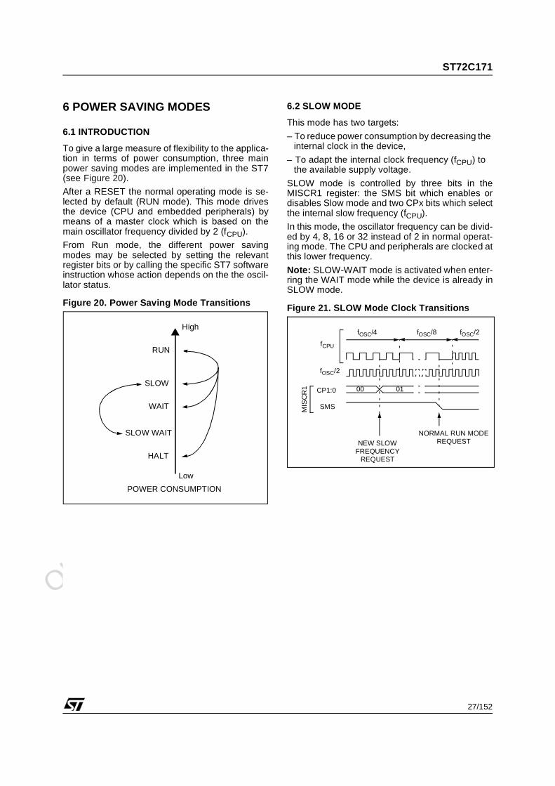
6.2 SLOW MODE
This mode has two targets:
– To reduce power consumption by decreasing the internal clock in the device,
– To adapt the internal clock frequency (fCPU) to the available supply voltage.
SLOW mode is controlled by three bits in theMISCR1 register: the SMS bit which enables ordisables Slow mode and two CPx bits which selectthe internal slow frequency (fCPU).
In this mode, the oscillator frequency can be divid-ed by 4, 8, 16 or 32 instead of 2 in normal operat-ing mode. The CPU and peripherals are clocked atthis lower frequency.
Note: SLOW-WAIT mode is activated when enter-ring the WAIT mode while the device is already inSLOW mode.
Figure 21. SLOW Mode Clock Transitions
POWER CONSUMPTION
WAIT
SLOW
RUN
HALT
High
Low
SLOW WAIT
00 01
SMS
CP1:0
fCPU
NEW SLOWNORMAL RUN MODE
MIS
CR
1
FREQUENCYREQUEST
REQUEST
fOSC/2
fOSC/4 fOSC/8 fOSC/2
Obsolete Product(
s) - O
bsolete Product(
s)
ST72C171
28/152
POWER SAVING MODES (Cont’d)
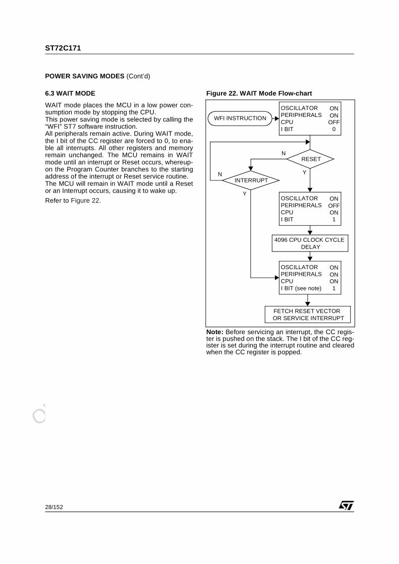
6.3 WAIT MODE
WAIT mode places the MCU in a low power con-sumption mode by stopping the CPU.This power saving mode is selected by calling the“WFI” ST7 software instruction.All peripherals remain active. During WAIT mode,the I bit of the CC register are forced to 0, to ena-ble all interrupts. All other registers and memoryremain unchanged. The MCU remains in WAITmode until an interrupt or Reset occurs, whereup-on the Program Counter branches to the startingaddress of the interrupt or Reset service routine. The MCU will remain in WAIT mode until a Resetor an Interrupt occurs, causing it to wake up.
Refer to Figure 22.
Figure 22. WAIT Mode Flow-chart
Note: Before servicing an interrupt, the CC regis-ter is pushed on the stack. The I bit of the CC reg-ister is set during the interrupt routine and clearedwhen the CC register is popped.
WFI INSTRUCTION
RESET
INTERRUPTY
N
N
Y
CPU
OSCILLATOR PERIPHERALS
I BIT
ONON
0OFF
FETCH RESET VECTOROR SERVICE INTERRUPT
CPU
OSCILLATOR PERIPHERALS
I BIT
ONOFF
1ON
CPU
OSCILLATOR PERIPHERALS
I BIT (see note)
ONON
1ON
4096 CPU CLOCK CYCLEDELAY
Obsolete Product(
s) - O
bsolete Product(
s)
ST72C171
29/152
POWER SAVING MODES (Cont’d)
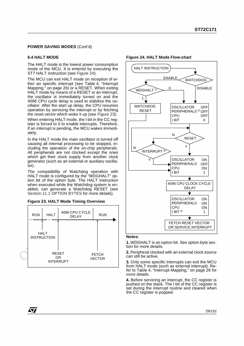
6.4 HALT MODE
The HALT mode is the lowest power consumptionmode of the MCU. It is entered by executing theST7 HALT instruction (see Figure 24).
The MCU can exit HALT mode on reception of ei-ther an specific interrupt (see Table 4, “InterruptMapping,” on page 26) or a RESET. When exitingHALT mode by means of a RESET or an interrupt,the oscillator is immediately turned on and the4096 CPU cycle delay is used to stabilize the os-cillator. After the start up delay, the CPU resumesoperation by servicing the interrupt or by fetchingthe reset vector which woke it up (see Figure 23).When entering HALT mode, the I bit in the CC reg-ister is forced to 0 to enable interrupts. Therefore,if an interrupt is pending, the MCU wakes immedi-ately.
In the HALT mode the main oscillator is turned offcausing all internal processing to be stopped, in-cluding the operation of the on-chip peripherals.All peripherals are not clocked except the oneswhich get their clock supply from another clockgenerator (such as an external or auxiliary oscilla-tor).
The compatibility of Watchdog operation withHALT mode is configured by the “WDGHALT” op-tion bit of the option byte. The HALT instructionwhen executed while the Watchdog system is en-abled, can generate a Watchdog RESET (seeSection 11.1 OPTION BYTES for more details).
Figure 23. HALT Mode Timing Overview
Figure 24. HALT Mode Flow-chart
Notes:1. WDGHALT is an option bit. See option byte sec-tion for more details.2. Peripheral clocked with an external clock sourcecan still be active.3. Only some specific interrupts can exit the MCUfrom HALT mode (such as external interrupt). Re-fer to Table 4, “Interrupt Mapping,” on page 26 formore details.4. Before servicing an interrupt, the CC register ispushed on the stack. The I bit of the CC register isset during the interrupt routine and cleared whenthe CC register is popped.
HALTRUN RUN4096 CPU CYCLE
DELAY
RESETOR
INTERRUPT
HALTINSTRUCTION
FETCHVECTOR
HALT INSTRUCTION
RESET
INTERRUPT 3)
Y
N
N
Y
CPU
OSCILLATOR PERIPHERALS 2)
I BIT
OFFOFF
0OFF
FETCH RESET VECTOROR SERVICE INTERRUPT
CPU
OSCILLATOR PERIPHERALS
I BIT
ONOFF
1ON
CPU
OSCILLATOR PERIPHERALS
I BIT 4)
ONON
1ON
4096 CPU CLOCK CYCLEDELAY
WATCHDOGENABLE
DISABLEWDGHALT 1) 0
WATCHDOGRESET
1
Obsolete Product(
s) - O
bsolete Product(
s)
ST72C171
30/152
7 ON-CHIP PERIPHERALS
7.1 I/O PORTS
7.1.1 Introduction
The I/O ports offer different functional modes:
– transfer of data through digital inputs and outputs
and for specific pins:
– analog signal input (ADC)
– alternate signal input/output for the on-chip pe-ripherals.
– external interrupt generation
An I/O port is composed of up to 8 pins. Each pincan be programmed independently as digital input(with or without interrupt generation) or digital out-put.
7.1.2 Functional Description
Each port is associated to 2 main registers:
– Data Register (DR)
– Data Direction Register (DDR)
and some of them to an optional register (see reg-ister description):
– Option Register (OR)
Each I/O pin may be programmed using the corre-sponding register bits in DDR and OR registers: bitX corresponding to pin X of the port. The same cor-respondence is used for the DR register.
The following description takes into account theOR register, for specific ports which do not providethis register refer to the I/O Port ImplementationSection 7.1.2.5. The generic I/O block diagram isshown on Figure 26.
7.1.2.1 Input Modes
The input configuration is selected by clearing thecorresponding DDR register bit.
In this case, reading the DR register returns thedigital value applied to the external I/O pin.
Different input modes can be selected by softwarethrough the OR register.
Notes:
1. All the inputs are triggered by a Schmitt trigger.
2. When switching from input mode to outputmode, the DR register should be written first tooutput the correct value as soon as the port is con-figured as an output.
Interrupt function
When an I/O is configured in Input with Interrupt,an event on this I/O can generate an external In-terrupt request to the CPU. The interrupt sensitivi-ty is given independently according to the descrip-tion mentioned in the Miscellaneous register or inthe interrupt register (where available).
Each pin can independently generate an Interruptrequest.
Each external interrupt vector is linked to a dedi-cated group of I/O port pins (see Interrupts sec-tion). If more than one input pin is selected simul-taneously as interrupt source, this is logicallyORed. For this reason if one of the interrupt pins istied low, it masks the other ones.
7.1.2.2 Output Mode
The pin is configured in output mode by setting thecorresponding DDR register bit.
In this mode, writing “0” or “1” to the DR registerapplies this digital value to the I/O pin through thelatch. Then reading the DR register returns thepreviously stored value.
Note: In this mode, the interrupt function is disa-bled.
7.1.2.3 Digital Alternate Function
When an on-chip peripheral is configured to use apin, the alternate function is automatically select-ed. This alternate function takes priority overstandard I/O programming. When the signal iscoming from an on-chip peripheral, the I/O pin isautomatically configured in output mode (push-pullor open drain according to the peripheral).
When the signal is going to an on-chip peripheral,the I/O pin has to be configured in input mode. Inthis case, the pin’s state is also digitally readableby addressing the DR register.
Notes:1. Input pull-up configuration can cause an unex-pected value at the input of the alternate peripher-al input.2. When the on-chip peripheral uses a pin as inputand output, this pin must be configured as an input(DDR = 0).
Warning: The alternate function must not be acti-vated as long as the pin is configured as input withinterrupt, in order to avoid generating spurious in-terrupts.
Obsolete Product(
s) - O
bsolete Product(
s)
ST72C171
31/152
I/O PORTS (Cont’d)
7.1.2.4 Analog Alternate Function When the pin is used as an ADC input the I/O mustbe configured as input, floating. The analog multi-plexer (controlled by the ADC registers) switchesthe analog voltage present on the selected pin tothe common analog rail which is connected to theADC input.
It is recommended not to change the voltage levelor loading on any port pin while conversion is inprogress. Furthermore it is recommended not tohave clocking pins located close to a selected an-alog pin.
Warning: The analog input voltage level must bewithin the limits stated in the Absolute MaximumRatings.
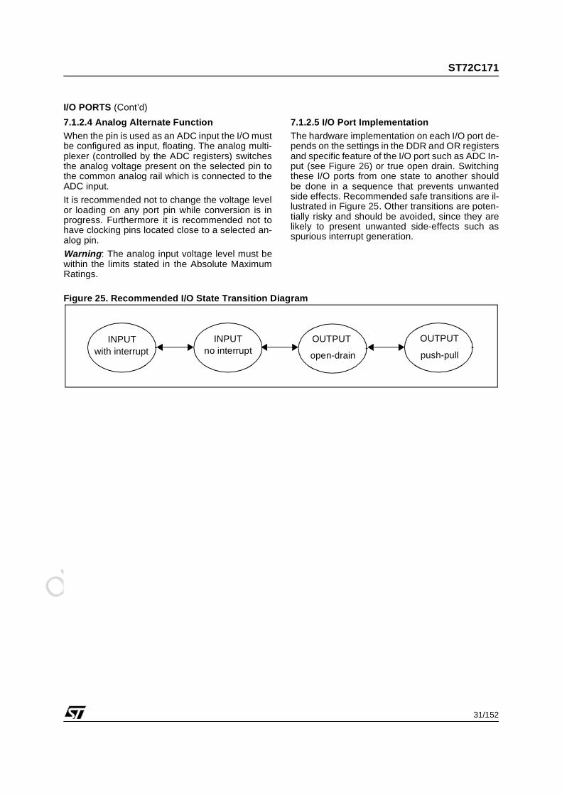
7.1.2.5 I/O Port ImplementationThe hardware implementation on each I/O port de-pends on the settings in the DDR and OR registersand specific feature of the I/O port such as ADC In-put (see Figure 26) or true open drain. Switchingthese I/O ports from one state to another shouldbe done in a sequence that prevents unwantedside effects. Recommended safe transitions are il-lustrated in Figure 25. Other transitions are poten-tially risky and should be avoided, since they arelikely to present unwanted side-effects such asspurious interrupt generation.
Figure 25. Recommended I/O State Transition Diagram
with interruptINPUT OUTPUT
no interruptINPUT
push-pullopen-drain
OUTPUT
Obsolete Product(
s) - O
bsolete Product(
s)
ST72C171
32/152
I/O PORTS (Cont’d)
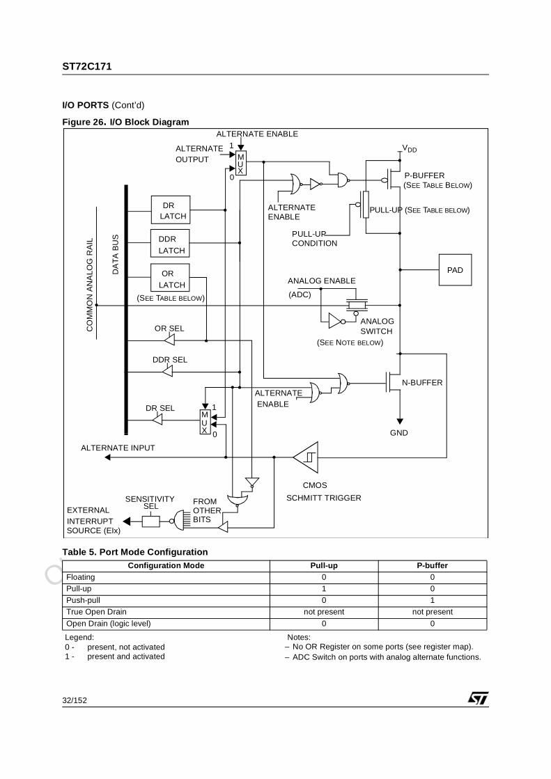
Figure 26. I/O Block Diagram
Table 5. Port Mode Configuration
Legend:0 - present, not activated1 - present and activated
Notes:– No OR Register on some ports (see register map).– ADC Switch on ports with analog alternate functions.
DR
DDR
LATCH
LATCH
DA
TA
BU
S
DR SEL
DDR SEL
VDD
PAD
ANALOGSWITCH
ANALOG ENABLE
(ADC)
MUX
ALTERNATE
ALTERNATE
ALTERNATE ENABLE
CO
MM
ON
AN
ALO
G R
AIL
ALTERNATE
MUX
ALTERNATE INPUT
PULL-UP (SEE TABLE BELOW)
OUTPUT
P-BUFFER (SEE TABLE BELOW)
N-BUFFER
1
0
1
0
ORLATCH
OR SEL
FROMOTHERBITS
EXTERNAL
PULL-UPCONDITION
ENABLE
ENABLE
GND
(SEE TABLE BELOW)
(SEE NOTE BELOW)
CMOS
SCHMITT TRIGGER
SOURCE (EIx)INTERRUPT
SENSITIVITYSEL
Configuration Mode Pull-up P-bufferFloating 0 0
Pull-up 1 0
Push-pull 0 1
True Open Drain not present not present
Open Drain (logic level) 0 0
Obsolete Product(
s) - O
bsolete Product(
s)
ST72C171
33/152
I/O PORTS (Cont’d)
7.1.2.6 Device Specific Configurations
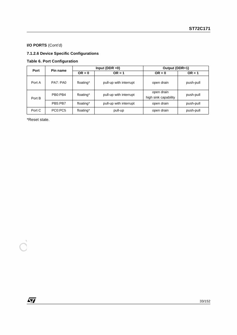
Table 6. Port Configuration
*Reset state.
Port Pin nameInput (DDR =0) Output (DDR=1)
OR = 0 OR = 1 OR = 0 OR = 1
Port A PA7: PA0 floating* pull-up with interrupt open drain push-pull
Port BPB0:PB4 floating* pull-up with interrupt
open drain
high sink capabilitypush-pull
PB5:PB7 floating* pull-up with interrupt open drain push-pull
Port C PC0:PC5 floating* pull-up open drain push-pull
Obsolete Product(
s) - O
bsolete Product(
s)
ST72C171
34/152
I/O PORTS (Cont’d)
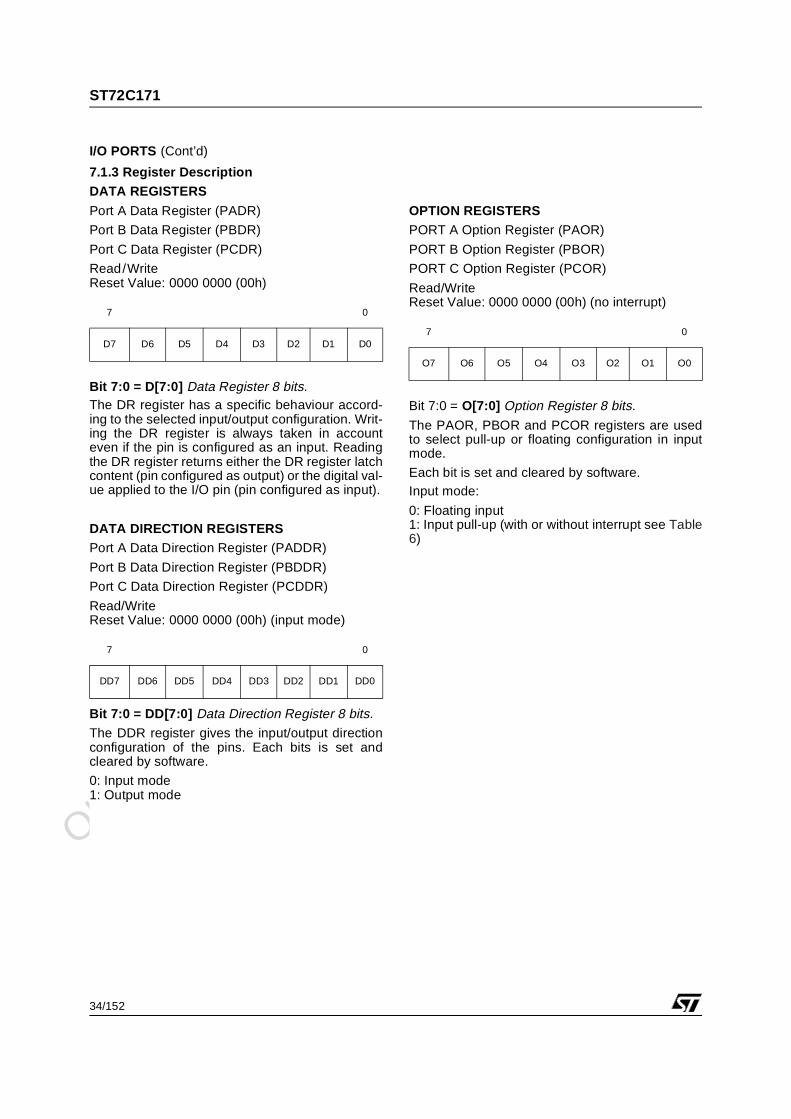
7.1.3 Register DescriptionDATA REGISTERS
Port A Data Register (PADR)
Port B Data Register (PBDR)
Port C Data Register (PCDR)
Read/WriteReset Value: 0000 0000 (00h)
Bit 7:0 = D[7:0] Data Register 8 bits.The DR register has a specific behaviour accord-ing to the selected input/output configuration. Writ-ing the DR register is always taken in accounteven if the pin is configured as an input. Readingthe DR register returns either the DR register latchcontent (pin configured as output) or the digital val-ue applied to the I/O pin (pin configured as input).
DATA DIRECTION REGISTERSPort A Data Direction Register (PADDR)
Port B Data Direction Register (PBDDR)
Port C Data Direction Register (PCDDR)
Read/WriteReset Value: 0000 0000 (00h) (input mode)
Bit 7:0 = DD[7:0] Data Direction Register 8 bits.The DDR register gives the input/output directionconfiguration of the pins. Each bits is set andcleared by software.
0: Input mode1: Output mode
OPTION REGISTERSPORT A Option Register (PAOR)
PORT B Option Register (PBOR)
PORT C Option Register (PCOR)
Read/WriteReset Value: 0000 0000 (00h) (no interrupt)
Bit 7:0 = O[7:0] Option Register 8 bits.
The PAOR, PBOR and PCOR registers are usedto select pull-up or floating configuration in inputmode.
Each bit is set and cleared by software.Input mode:
0: Floating input1: Input pull-up (with or without interrupt see Table6)
7 0
D7 D6 D5 D4 D3 D2 D1 D0
7 0
DD7 DD6 DD5 DD4 DD3 DD2 DD1 DD0
7 0
O7 O6 O5 O4 O3 O2 O1 O0
Obsolete Product(
s) - O
bsolete Product(
s)
ST72C171
35/152
I/O PORTS (Cont’d)
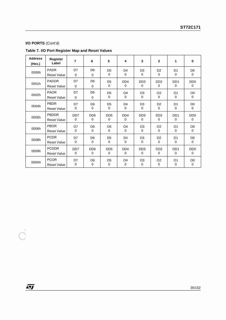
Table 7. I/O Port Register Map and Reset Values
Address
(Hex.)Register
Label7 6 5 4 3 2 1 0
0000hPADR
Reset Value
D7
0
D6
0D50
D40
D30
D20
D10
D00
0001hPADDR
Reset Value
D7
0
D6
0D50
DD40
DD30
DD20
DD10
DD00
0002hPAOR
Reset Value
D7
0
D6
0D50
O40
O30
O20
O10
O00
0004hPBDR
Reset ValueD70
D60
D50
D40
D30
D20
D10
D00
0005hPBDDR
Reset ValueDD7
0DD6
0DD5
0DD4
0DD3
0DD2
0DD1
0DD0
0
0006hPBOR
Reset ValueO70
O60
O50
O40
O30
O20
O10
O00
0008hPCDR
Reset ValueD70
D60
D50
D40
D30
D20
D10
D00
0009hPCDDR
Reset ValueDD7
0DD6
0DD5
0DD4
0DD3
0DD2
0DD1
0DD0
0
000AhPCOR
Reset ValueO70
O60
O50
O40
O30
O20
O10
O00
Obsolete Product(
s) - O
bsolete Product(
s)
ST72C171
36/152
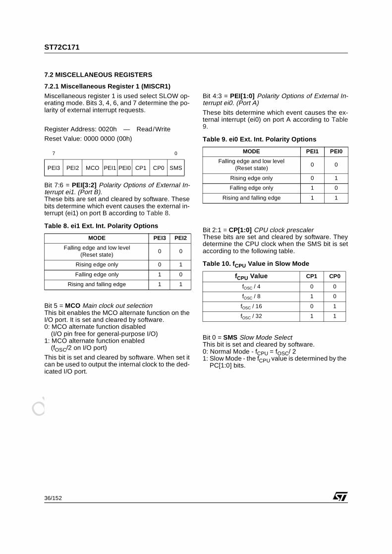
7.2 MISCELLANEOUS REGISTERS
7.2.1 Miscellaneous Register 1 (MISCR1)
Miscellaneous register 1 is used select SLOW op-erating mode. Bits 3, 4, 6, and 7 determine the po-larity of external interrupt requests.
Register Address: 0020h — Read/Write
Reset Value: 0000 0000 (00h)
Bit 7:6 = PEI[3:2] Polarity Options of External In-terrupt ei1. (Port B). These bits are set and cleared by software. Thesebits determine which event causes the external in-terrupt (ei1) on port B according to Table 8.
Table 8. ei1 Ext. Int. Polarity Options
Bit 5 = MCO Main clock out selectionThis bit enables the MCO alternate function on theI/O port. It is set and cleared by software.0: MCO alternate function disabled
(I/O pin free for general-purpose I/O)1: MCO alternate function enabled
(fOSC/2 on I/O port)
This bit is set and cleared by software. When set itcan be used to output the internal clock to the ded-icated I/O port.
Bit 4:3 = PEI[1:0] Polarity Options of External In-terrupt ei0. (Port A)
These bits determine which event causes the ex-ternal interrupt (ei0) on port A according to Table9.
Table 9. ei0 Ext. Int. Polarity Options
Bit 2:1 = CP[1:0] CPU clock prescalerThese bits are set and cleared by software. Theydetermine the CPU clock when the SMS bit is setaccording to the following table.
Table 10. fCPU Value in Slow Mode
Bit 0 = SMS Slow Mode SelectThis bit is set and cleared by software.0: Normal Mode - fCPU = fOSC/ 2 1: Slow Mode - the fCPU value is determined by the
PC[1:0] bits.
7 0
PEI3 PEI2 MCO PEI1 PEI0 CP1 CP0 SMS
MODE PEI3 PEI2
Falling edge and low level(Reset state)
0 0
Rising edge only 0 1
Falling edge only 1 0
Rising and falling edge 1 1
MODE PEI1 PEI0
Falling edge and low level (Reset state)
0 0
Rising edge only 0 1
Falling edge only 1 0
Rising and falling edge 1 1
fCPU Value CP1 CP0
fOSC / 4 0 0
fOSC / 8 1 0
fOSC / 16 0 1
fOSC / 32 1 1
Obsolete Product(
s) - O
bsolete Product(
s)
ST72C171
37/152
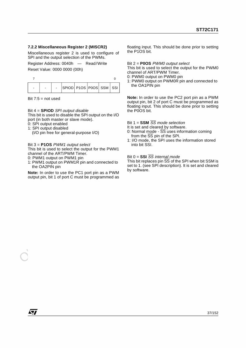
7.2.2 Miscellaneous Register 2 (MISCR2)
Miscellaneous register 2 is used to configure ofSPI and the output selection of the PWMs.
Register Address: 0040h — Read/Write
Reset Value: 0000 0000 (00h)
Bit 7:5 = not used
Bit 4 = SPIOD SPI output disableThis bit is used to disable the SPI output on the I/Oport (in both master or slave mode).0: SPI output enabled1: SPI output disabled
(I/O pin free for general-purpose I/O)
Bit 3 = P1OS PWM1 output selectThis bit is used to select the output for the PWM1channel of the ART/PWM Timer.0: PWM1 output on PWM1 pin1: PWM1 output on PWM1R pin and connected to
the OA2PIN pin
Note: In order to use the PC1 port pin as a PWMoutput pin, bit 1 of port C must be programmed as
floating input. This should be done prior to settingthe P1OS bit.
Bit 2 = P0OS PWM0 output selectThis bit is used to select the output for the PWM0channel of ART/PWM Timer.0: PWM0 output on PWM0 pin1: PWM0 output on PWM0R pin and connected to
the OA1PIN pin
Note: In order to use the PC2 port pin as a PWMoutput pin, bit 2 of port C must be programmed asfloating input. This should be done prior to settingthe P0OS bit.
Bit 1 = SSM SS mode selectionIt is set and cleared by software.0: Normal mode - SS uses information coming
from the SS pin of the SPI.1: I/O mode, the SPI uses the information stored
into bit SSI.
Bit 0 = SSI SS internal modeThis bit replaces pin SS of the SPI when bit SSM isset to 1. (see SPI description). It is set and clearedby software.
7 0
- - - SPIOD P1OS P0OS SSM SSI
Obsolete Product(
s) - O
bsolete Product(
s)
ST72C171
38/152
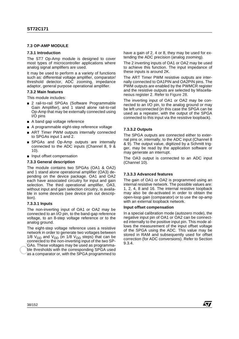
7.3 OP-AMP MODULE
7.3.1 Introduction
The ST7 Op-Amp module is designed to covermost types of microcontroller applications whereanalog signal amplifiers are used.
It may be used to perform a a variety of functionssuch as: differential voltage amplifier, comparator/threshold detector, ADC zooming, impedanceadaptor, general purpose operational amplifier.
7.3.2 Main featuresThis module includes: 2 rail-to-rail SPGAs (Software Programmable
Gain Amplifier), and 1 stand alone rail-to-railOp-Amp that may be externally connected usingI/O pins
A band gap voltage reference A programmable eight-step reference voltage ART Timer PWM outputs internally connected
to SPGAs input 1 and 2. SPGAs and Op-Amp outputs are internally
connected to the ADC inputs (Channel 8, 9 &10).
Input offset compensation
7.3.3 General descriptionThe module contains two SPGAs (OA1 & OA2)and 1 stand alone operational amplifier (OA3) de-pending on the device package. OA1 and OA2each have associated circuitry for input and gainselection. The third operational amplifier, OA3,without input and gain selection circuitry, is availa-ble in some devices (see device pin out descrip-tion).
7.3.3.1 Inputs
The non-inverting input of OA1 or OA2 may beconnected to an I/O pin, to the band-gap referencevoltage, to an 8-step voltage reference or to theanalog ground.
The eight-step voltage reference uses a resistivenetwork in order to generate two voltages between1/8 VDD and VDD (in 1/8 VDD steps) that can beconnected to the non-inverting input of the two SP-GAs. These voltages may be used as programma-ble thresholds with the corresponding SPGA usedas a comparator or, with the SPGA programmed to
have a gain of 2, 4 or 8, they may be used for ex-tending the ADC precision (analog zooming).
The 2 inverting inputs of OA1 or OA2 may be usedto achieve this function. The input impedance ofthese inputs is around 2K.
The ART Timer PWM resistive outputs are inter-nally connected to OA1PIN and OA2PIN pins. ThePWM outputs are enabled by the PWMCR registerand the resistive outputs are selected by Miscella-neous register 2. Refer to Figure 28.
The inverting input of OA1 or OA2 may be con-nected to an I/O pin, to the analog ground or maybe left unconnected (in this case the SPGA can beused as a repeater, with the output of the SPGAconnected to this input via the resistive loopback).
7.3.3.2 OutputsThe SPGA outputs are connected either to exter-nal pins or, internally, to the ADC input (Channel 8& 9). The output value, digitized by a Schmitt trig-ger, may be read by the application software ormay generate an interrupt.
The OA3 output is connected to an ADC input(Channel 10).
7.3.3.3 Advanced featuresThe gain of OA1 or OA2 is programmed using aninternal resistive network. The possible values are:1, 2, 4, 8 and 16. The internal resistive loopbackmay also be de-activated in order to obtain theopen-loop gain (comparator) or to use the op-ampwith an external loopback network.
Input offset compensation
In a special calibration mode (autozero mode), thenegative input pin of OA1 or OA2 can be connect-ed internally to the positive input pin. This mode al-lows the measurement of the input offset voltageof the SPGA using the ADC. This value may bestored in RAM and subsequently used for offsetcorrection (for ADC conversions). Refer to Section9.3.4.
Obsolete Product(
s) - O
bsolete Product(
s)
ST72C171
39/152
OP-AMP MODULE (Cont’d)
Figure 27. Op-Amp Module Block Diagram
OA1NIN
OA1
R=2K
15R /16R
R
AVCL=1, 2, 4, 8, 16, ∞
R=2K
OA1V
(1.2V)
OA1O
OA1PINTo ADC Channel 8
NS1[2:0] bits
AZ1 bit
G1[2:0] bits
VR1E, PS1[1:0] bits
VR1[2:0] bitsx VDDA/8
OA1Interrupt
OA1IE bit
bit8-Step Reference
Voltage 1
Band GapReferenceVoltage
OA2NIN
OA2
R=2K
15R /16R
R
AVCL=1, 2, 4, 8, 16, ∞
R=2K
OA2V
(1.2V)
VSSA
OA2O
OA2PINTo ADC Channel 9
NS2[2:0] bits
AZ2 bit
G2[2:0] bits
VR2E, PS2[1:0] bits
VR2[2:0] bitsx VDDA/8
OA2Interrupt
OA2IE bit
bit8-Step Reference
Voltage 2
Band GapReferenceVoltage
OA3
OA3O
OA3NIN To ADC Channel 10
OA3PIN
Note: OA3 is not present on some package types. Refer to the device pin description.
VSSA
ART Timer PWM0R Output
ART Timer PWM1R Output
Obsolete Product(
s) - O
bsolete Product(
s)
ST72C171
40/152
OP-AMP MODULE (Cont’d)
7.3.4 Autozero Mode
When the following description refers to both OA1or OA2, x stands for 1 or 2.
In order to eliminate the ADC errors due to theSPGA offset voltage, this voltage may be deter-mined, prior to the A/D conversion (at power on orperiodically) and stored in RAM. The stored valuemay be used afterwards to eliminate the errors ofany A/D conversion that uses the SPGA (ADCzooming). The measurement may be done inde-pendently for OA1 and OA2.
The measurement algorithm has 3 steps:
1. The SPGA is in repeater mode (NSx[1:0] = 01),with the lowest gain (Gx[2:0]=000), the autoze-roing switch is left open (AZx = 0). The positiveinput of the op-amp is connected to a DC value,using the VRx reference voltage generator(PSx[1:0] = 00), and the output is sent to theADC. Under these conditions, the ADC meas-ures the value:
Vo = VRx -Voff
of the SPGA output.
2. Set the gain (G) according the applicationrequirement. The AZx bit is set to 1. The outputvoltage of the SPGA becomes:
V’o = VRx - Voff - G * Voff
3.Voff calculated with 1) - 2)
Voff =( Vo- V’o) /G
As the offset voltage of the SPGAs may vary withthe common mode voltage value, the measure-ment must be done choosing VRx to match the ap-plication conditions. Alternatively, nine measure-ments may be done with the noninverting inputvoltage varying between 0 and VDDA in 1/8 VDDsteps, in order to fully characterise the offset volt-age of the op-amp.
7.3.5 Comparator mode with Interrupts
The 2 SPGAs can be configured in comparatormode (GX[2:0]=111). In this case the positive in-put can be connected to the internal referencevoltage. The negative input can be used to receivethe analog voltage to be compared with the volt-age connected to the positive input.
By means of a Schmitt trigger, the SPGA output isreadable as a logical level in the OAxVR bit in theOAIRR register. These bits are read only.
An interrupt request remains pending as long asthe output value (OAxVR) is equal to the corre-sponding polarity bit (OAxPR) and when the inter-rupt enable bit (OAxIE) is set. There is one inter-rupt vector for each SPGA.
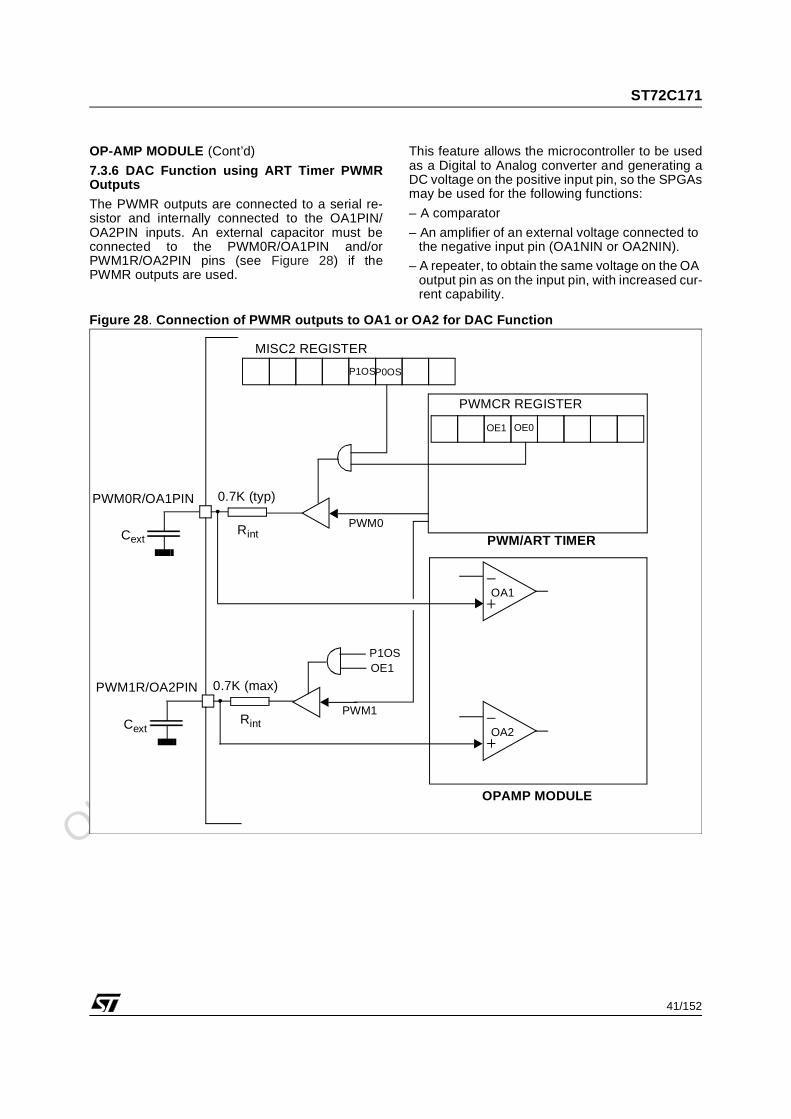
Obsolete Product(
s) - O
bsolete Product(
s)
ST72C171
41/152
OP-AMP MODULE (Cont’d)
7.3.6 DAC Function using ART Timer PWMROutputs
The PWMR outputs are connected to a serial re-sistor and internally connected to the OA1PIN/OA2PIN inputs. An external capacitor must beconnected to the PWM0R/OA1PIN and/orPWM1R/OA2PIN pins (see Figure 28) if thePWMR outputs are used.
This feature allows the microcontroller to be usedas a Digital to Analog converter and generating aDC voltage on the positive input pin, so the SPGAsmay be used for the following functions:
– A comparator
– An amplifier of an external voltage connected to the negative input pin (OA1NIN or OA2NIN).
– A repeater, to obtain the same voltage on the OA output pin as on the input pin, with increased cur-rent capability.
Figure 28. Connection of PWMR outputs to OA1 or OA2 for DAC Function
0.7K (typ)
CextRint PWM/ART TIMER
OA2
OPAMP MODULE
OA1
0.7K (max)
CextRint
PWM1
PWM0R/OA1PIN
PWM1R/OA2PIN
MISC2 REGISTER
P1OSP0OS
OE1 OE0
PWMCR REGISTER
PWM0
P1OSOE1
Obsolete Product(
s) - O
bsolete Product(
s)
ST72C171
42/152
OP-AMP MODULE (Cont’d)
7.3.7 Low Power Modes
Note: Low Power modes have no effect on the SPGAs & the Op-Amp. They can be switched off to reducethe power consumption of the ST7 (OAxON bits).
7.3.8 Interrupts
* The interrupt event occurs when the OAxP bit equals the OAxV bit value.
Note: The SPGA interrupt events are connected to 2 interrupt vectors (see Interrupts chapter). Theseevents generate an interrupt if the corresponding Enable Control Bit is set and the interrupt mask in theCC register is reset (RIM instruction).
Mode Description
WAITNo effect on op-amp. SPGA interrupts cause the device to exit from WAIT mode.
HALTNo effect on op-amp.SPGA interrupts cause the device to exit from HALT mode.
Interrupt EventEventFlag
Enable Control
Bit
Exit fromWait
Exit from Halt
Op-Amp 1 output in comparator mode equals to OA1P bit value NA* OA1IE Yes Yes
Op-Amp 2 output in comparator mode equals to OA2P bit value NA* OA2IE Yes Yes
Obsolete Product(
s) - O
bsolete Product(
s)
ST72C171
43/152
7.3.9 Register Description
OA1 CONTROL REGISTER (OA1CR)Read/WriteReset value: 0000 00000 (00h)
Bit 7 = AZ1 OA1 Autozero Mode.
This bit is set and reset by hardware. It enablesAutozero mode (used to measure the OA1 inputoffset).0: Autozero mode disabled 1: Autozero mode enabled
Bit 6:4 = G1[2:0] Gain Control.These bits are set and reset by software and con-trol the OA1 gain by modifying the resistive loop-back network. The value of the gain is adjusted tothe desired value (for inverting / non-inverting am-plification) corresponding to the selected positiveinput source - see PS1[1:0] table, Gain Adjust col-umn.
Bit 3:2 = PS1[1:0] Positive Input Select / Gain ad-just.These bits are set and reset by software and con-trol the OA1 positive input selection.
Bit 1:0 = NS1[1:0] Negative Input Select.
These bits are set and reset by software and con-trol the OA1 positive input selection.
OA2 CONTROL REGISTER (OA2CR)Read/WriteReset value: 0000 0000 (00h)
Bit 7 = AZ2 OA2 Autozero Mode.This bit is set and reset by hardware. It enablesAutozero mode (used to measure the OA2 inputoffset).0: Autozero mode disabled 1: Autozero mode enabled
Bit 6:4 = G2[2:0] Gain Control.These bits are set and reset by software and con-trol the OA2 gain by modifying the resistive loop-back network. The value of the gain is adjusted tothe desired value (for inverting/noninverting ampli-fication) corresponding to the selected positive in-put source - see PS2[1:0] table, Gain Adjust col-umn.
7 0
AZ1 G12 G11 G10 PS11 PS10 NS11 NS10
Gain
inv / NinvG12 G11 G10
-1 / 2 0 0 0
-2 / 3 0 0 1
-3 / 4 0 1 0
-4 / 5 0 1 1
-8 / 8 1 0 0
-16 / 16 1 0 1
ComparatorExternal Loopback
1 1 1
OA1 Positive Input Gain Adj.
PS11 PS10
8-step Ref.Voltage 1 inv 0 0
OA1PIN ninv 0 1
Band Gap Ref. Voltage (1.2V) inv 1 0
OA1 Negative Input NS11 NS10AGND 0 0
Floating - Repeater mode 0 1
OA1NIN 1 X
7 0
AZ2 G22 G21 G20 PS21 PS20 NS21 NS20
Gain
inv / NinvG22 G21 G20
-1 / 2 0 0 0
-2 / 3 0 0 1
-3 / 4 0 1 0
-4 / 5 0 1 1
-8 / 8 1 0 0
-16 / 16 1 0 1
ComparatorExternal Loopback
1 1 1
Obsolete Product(
s) - O
bsolete Product(
s)
ST72C171
44/152
OP-AMP MODULE (Cont’d)
Bit 3:2 = PS2[1:0] Positive Input Select / Gain ad-just.
These bits are set and reset by software and con-trol the OA2 positive input selection.t
Bit 1:0 = NS2[1:0] Negative Input Select.
These bits are set and reset by software and con-trol the OA2 negative input selection.
OA3 CONTROL REGISTER (OA3CR)Read/WriteReset value: 0000 0000 (00h)
Bit 7 = OA3ON OA3 on/off (low power)Stand Alone Op-Amp on/off control bit, it is set andreset by software. It reduces power consumptionwhen reset.0: Op-amp 3 off 1: Op-amp 3 on
Note: This bit must be kept cleared in deviceswithout OA3 (refer to device block diagram and pindescription)
Bit 6:0 = Reserved.
OA2 Positive Input Gain Adj.
PS21 PS20
8-step Ref.Voltage 1 inv 0 0
OA2PIN ninv 0 1
Band Gap Ref. Voltage (1.2V) inv 1 0
Floating ninv 1 1
OA2 Negative Input NS21 NS20AGND 0 0
Floating -Repeater mode 0 1
OA2NIN 1 X
7 0
OA3ON - - - - - - -
Obsolete Product(
s) - O
bsolete Product(
s)
ST72C171
45/152
OP-AMP MODULE (Cont’d)
OP-AMP INTERRUPT AND READOUT REGIS-TER (OAIRR) Read/Write*Reset value: 0000 0000 (00h)
Bit 7 = OA1IE OA1 interrupt enableThis bit is set and reset by software. When it is set,it enables an interrupt to be generated if the OA1Pbit and the OA1V bit have the same value.0: OA1 interrupt disabled1: OA1 interrupt enabled
Bit 6 = OA1P OA1 interrupt polarity selectThis bit is set and reset by software. It specifies theOA1 SPGA output level which will generate an in-terrupt if the bit OA1IE is set.0: Active low1: Active high
Bit 5 = OA1V OA1 output value (read only)This bit is set and reset by hardware. It containsthe OA1 SPGA output voltage value filtered by aSchmitt trigger.0: OA1+ voltage < OA1- voltage1: OA1+ voltage > OA1- voltage
Bit 4 = OA1ON OA1 on/off (low power)
This bit is set and reset by software. It reducespower consumption when reset.0: Op-amp 1 off 1: Op-amp 1 on
Bit 3 = OA2IE OA2 interrupt enableThis bit is set and reset by software. When it is set,it enables an interrupt to be generated if the OA2Pbit and the OA2V bit have the same value.0: OA2 interrupt disabled1: OA2 interrupt enabled
Bit 2 = OA2P OA2 interrupt polarity selectThis bit is set and reset by software. It specifies theOA2 SPGA output level which will generate an in-terrupt if the bit OA2IE is set.0: Active low1: Active high
Bit 1- OA2V OA2 output value (read only)This bit is set and reset by hardware. It containsthe OA2 SPGA output voltage value filtered by aSchmitt trigger.0: OA2+ voltage < OA2- voltage1: OA2+ voltage > OA2- voltage
Bit 0 - OA2ON OA2 on/off (low power)0: Op-amp 2 off (reducing power consumption)1: Op-amp 2 on
Note: If OA1ON, OA2ON and OA3ON are 0, Theentire module is disabled, giving the lowest powerconsumption.
* OA1V and OA2V are read only.
7 0
OA1IE OA1P OA1V OA1ON OA2IE OA2P OA2V OA2ON
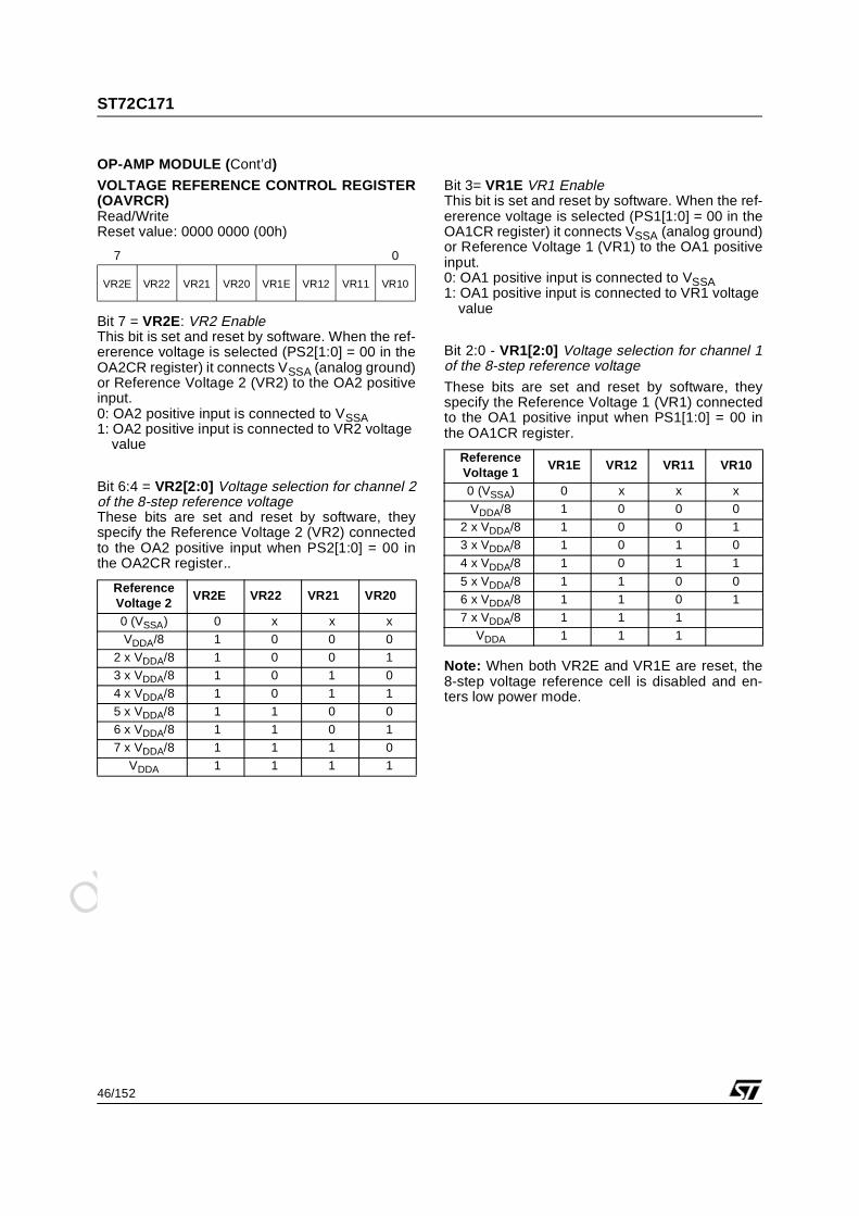
Obsolete Product(
s) - O
bsolete Product(
s)
ST72C171
46/152
OP-AMP MODULE (Cont’d)
VOLTAGE REFERENCE CONTROL REGISTER(OAVRCR)Read/WriteReset value: 0000 0000 (00h)
Bit 7 = VR2E: VR2 EnableThis bit is set and reset by software. When the ref-ererence voltage is selected (PS2[1:0] = 00 in theOA2CR register) it connects VSSA (analog ground)or Reference Voltage 2 (VR2) to the OA2 positiveinput. 0: OA2 positive input is connected to VSSA1: OA2 positive input is connected to VR2 voltage
value
Bit 6:4 = VR2[2:0] Voltage selection for channel 2of the 8-step reference voltageThese bits are set and reset by software, theyspecify the Reference Voltage 2 (VR2) connectedto the OA2 positive input when PS2[1:0] = 00 inthe OA2CR register..
Bit 3= VR1E VR1 EnableThis bit is set and reset by software. When the ref-ererence voltage is selected (PS1[1:0] = 00 in theOA1CR register) it connects VSSA (analog ground)or Reference Voltage 1 (VR1) to the OA1 positiveinput. 0: OA1 positive input is connected to VSSA1: OA1 positive input is connected to VR1 voltage
value
Bit 2:0 - VR1[2:0] Voltage selection for channel 1of the 8-step reference voltage
These bits are set and reset by software, theyspecify the Reference Voltage 1 (VR1) connectedto the OA1 positive input when PS1[1:0] = 00 inthe OA1CR register.
Note: When both VR2E and VR1E are reset, the8-step voltage reference cell is disabled and en-ters low power mode.
7 0
VR2E VR22 VR21 VR20 VR1E VR12 VR11 VR10
Reference Voltage 2
VR2E VR22 VR21 VR20
0 (VSSA) 0 x x x
VDDA/8 1 0 0 0
2 x VDDA/8 1 0 0 1
3 x VDDA/8 1 0 1 0
4 x VDDA/8 1 0 1 1
5 x VDDA/8 1 1 0 0
6 x VDDA/8 1 1 0 1
7 x VDDA/8 1 1 1 0
VDDA 1 1 1 1
Reference Voltage 1
VR1E VR12 VR11 VR10
0 (VSSA) 0 x x x
VDDA/8 1 0 0 0
2 x VDDA/8 1 0 0 1
3 x VDDA/8 1 0 1 0
4 x VDDA/8 1 0 1 1
5 x VDDA/8 1 1 0 0
6 x VDDA/8 1 1 0 1
7 x VDDA/8 1 1 1
VDDA 1 1 1
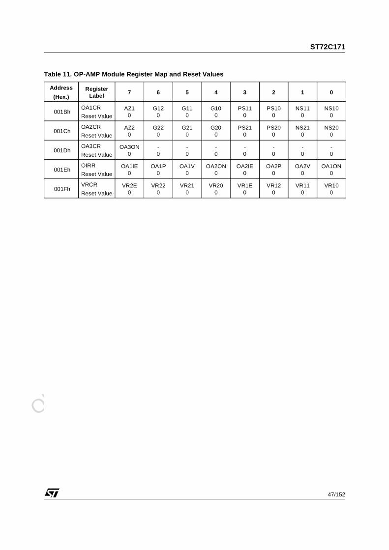
Obsolete Product(
s) - O
bsolete Product(
s)
ST72C171
47/152
Table 11. OP-AMP Module Register Map and Reset Values
Address
(Hex.)Register
Label7 6 5 4 3 2 1 0
001BhOA1CR
Reset ValueAZ1
0G12
0G11
0G10
0PS11
0PS10
0NS11
0NS10
0
001ChOA2CR
Reset ValueAZ2
0G22
0G21
0G20
0PS21
0PS20
0NS21
0NS20
0
001DhOA3CR
Reset ValueOA3ON
0-0
-0
-0
-0
-0
-0
-0
001EhOIRR
Reset ValueOA1IE
0OA1P
0OA1V
0OA2ON
0OA2IE
0OA2P
0OA2V
0OA1ON
0
001FhVRCR
Reset ValueVR2E
0VR22
0VR21
0VR20
0VR1E
0VR12
0VR11
0VR10
0
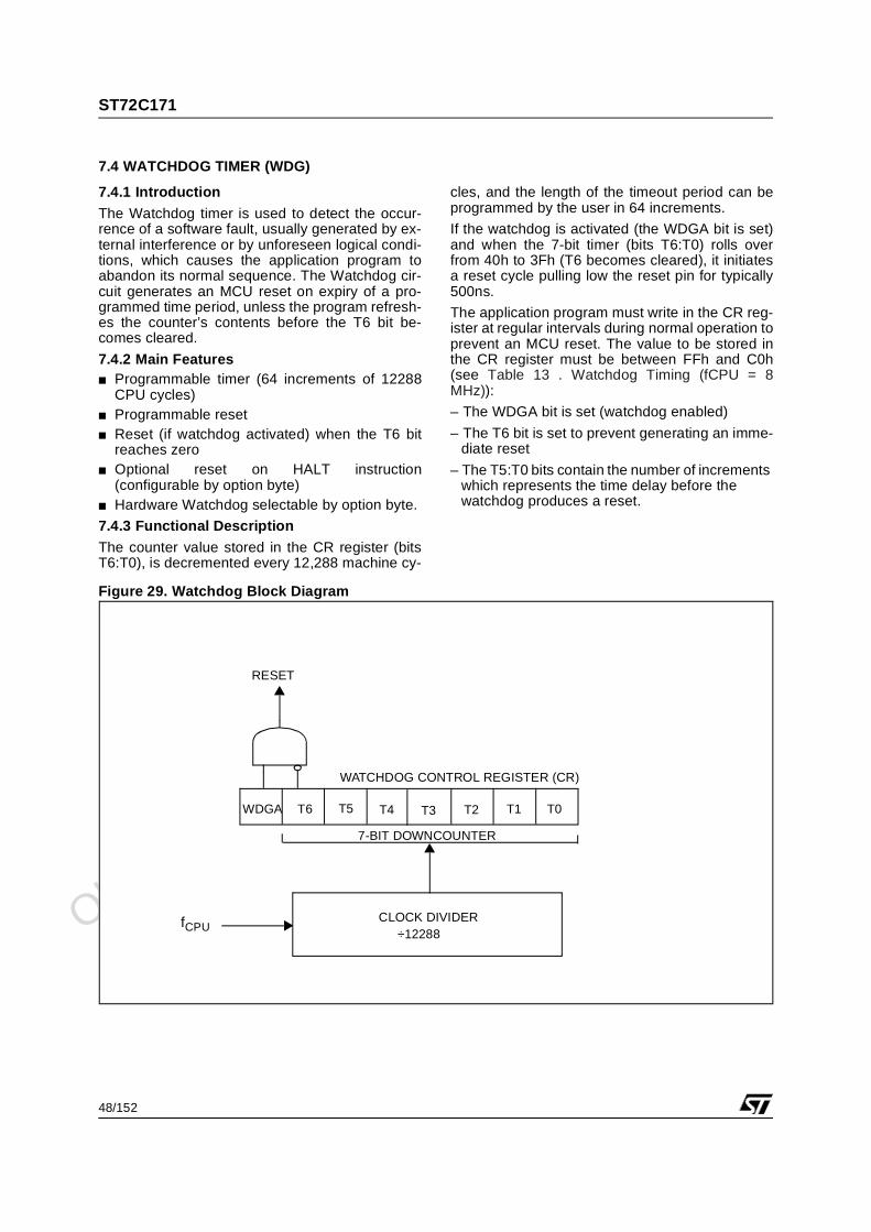
Obsolete Product(
s) - O
bsolete Product(
s)
ST72C171
48/152
7.4 WATCHDOG TIMER (WDG)
7.4.1 Introduction
The Watchdog timer is used to detect the occur-rence of a software fault, usually generated by ex-ternal interference or by unforeseen logical condi-tions, which causes the application program toabandon its normal sequence. The Watchdog cir-cuit generates an MCU reset on expiry of a pro-grammed time period, unless the program refresh-es the counter’s contents before the T6 bit be-comes cleared.
7.4.2 Main Features Programmable timer (64 increments of 12288
CPU cycles) Programmable reset Reset (if watchdog activated) when the T6 bit
reaches zero Optional reset on HALT instruction
(configurable by option byte) Hardware Watchdog selectable by option byte.
7.4.3 Functional Description
The counter value stored in the CR register (bitsT6:T0), is decremented every 12,288 machine cy-
cles, and the length of the timeout period can beprogrammed by the user in 64 increments.
If the watchdog is activated (the WDGA bit is set)and when the 7-bit timer (bits T6:T0) rolls overfrom 40h to 3Fh (T6 becomes cleared), it initiatesa reset cycle pulling low the reset pin for typically500ns.
The application program must write in the CR reg-ister at regular intervals during normal operation toprevent an MCU reset. The value to be stored inthe CR register must be between FFh and C0h(see Table 13 . Watchdog Timing (fCPU = 8MHz)):
– The WDGA bit is set (watchdog enabled)
– The T6 bit is set to prevent generating an imme-diate reset
– The T5:T0 bits contain the number of increments which represents the time delay before the watchdog produces a reset.
Figure 29. Watchdog Block Diagram
RESET
WDGA
7-BIT DOWNCOUNTER
fCPU
T6 T0
CLOCK DIVIDER
WATCHDOG CONTROL REGISTER (CR)
÷12288
T1T2T3T4T5
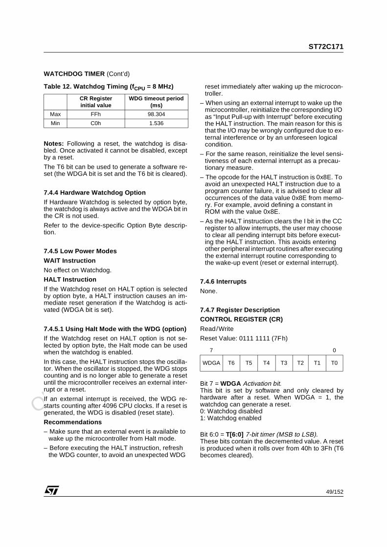
Obsolete Product(
s) - O
bsolete Product(
s)
ST72C171
49/152
WATCHDOG TIMER (Cont’d)
Table 12. Watchdog Timing (fCPU = 8 MHz)
Notes: Following a reset, the watchdog is disa-bled. Once activated it cannot be disabled, exceptby a reset.
The T6 bit can be used to generate a software re-set (the WDGA bit is set and the T6 bit is cleared).
7.4.4 Hardware Watchdog Option
If Hardware Watchdog is selected by option byte,the watchdog is always active and the WDGA bit inthe CR is not used.
Refer to the device-specific Option Byte descrip-tion.
7.4.5 Low Power Modes
WAIT Instruction
No effect on Watchdog.
HALT Instruction
If the Watchdog reset on HALT option is selectedby option byte, a HALT instruction causes an im-mediate reset generation if the Watchdog is acti-vated (WDGA bit is set).
7.4.5.1 Using Halt Mode with the WDG (option)If the Watchdog reset on HALT option is not se-lected by option byte, the Halt mode can be usedwhen the watchdog is enabled.
In this case, the HALT instruction stops the oscilla-tor. When the oscillator is stopped, the WDG stopscounting and is no longer able to generate a resetuntil the microcontroller receives an external inter-rupt or a reset.
If an external interrupt is received, the WDG re-starts counting after 4096 CPU clocks. If a reset isgenerated, the WDG is disabled (reset state).
Recommendations– Make sure that an external event is available to
wake up the microcontroller from Halt mode.
– Before executing the HALT instruction, refresh the WDG counter, to avoid an unexpected WDG
reset immediately after waking up the microcon-troller.
– When using an external interrupt to wake up the microcontroller, reinitialize the corresponding I/O as “Input Pull-up with Interrupt” before executing the HALT instruction. The main reason for this is that the I/O may be wrongly configured due to ex-ternal interference or by an unforeseen logical condition.
– For the same reason, reinitialize the level sensi-tiveness of each external interrupt as a precau-tionary measure.
– The opcode for the HALT instruction is 0x8E. To avoid an unexpected HALT instruction due to a program counter failure, it is advised to clear all occurrences of the data value 0x8E from memo-ry. For example, avoid defining a constant in ROM with the value 0x8E.
– As the HALT instruction clears the I bit in the CC register to allow interrupts, the user may choose to clear all pending interrupt bits before execut-ing the HALT instruction. This avoids entering other peripheral interrupt routines after executing the external interrupt routine corresponding to the wake-up event (reset or external interrupt).
7.4.6 Interrupts
None.
7.4.7 Register DescriptionCONTROL REGISTER (CR)
Read/Write
Reset Value: 0111 1111 (7Fh)
Bit 7 = WDGA Activation bit.This bit is set by software and only cleared byhardware after a reset. When WDGA = 1, thewatchdog can generate a reset.0: Watchdog disabled1: Watchdog enabled
Bit 6:0 = T[6:0] 7-bit timer (MSB to LSB).These bits contain the decremented value. A resetis produced when it rolls over from 40h to 3Fh (T6becomes cleared).
CR Register initial value
WDG timeout period (ms)
Max FFh 98.304
Min C0h 1.536
7 0
WDGA T6 T5 T4 T3 T2 T1 T0
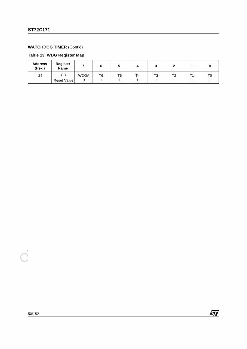
Obsolete Product(
s) - O
bsolete Product(
s)
ST72C171
50/152
WATCHDOG TIMER (Cont’d)
Table 13. WDG Register Map
Address(Hex.)
Register Name
7 6 5 4 3 2 1 0
24 CR
Reset ValueWDGA
0T61
T51
T41
T31
T21
T11
T01
Obsolete Product(
s) - O
bsolete Product(
s)
ST72C171
51/152
7.5 16-BIT TIMER
7.5.1 Introduction
The timer consists of a 16-bit free-running counterdriven by a programmable prescaler.
It may be used for a variety of purposes, includingmeasuring the pulse lengths of up to two input sig-nals (input capture) or generating up to two outputwaveforms (output compare and PWM).
Pulse lengths and waveform periods can be mod-ulated from a few microseconds to several milli-seconds using the timer prescaler and the CPUclock prescaler.
Some ST7 devices have two on-chip 16-bit timers.They are completely independent, and do notshare any resources. They are synchronized aftera MCU reset as long as the timer clock frequen-cies are not modified.
This description covers one or two 16-bit timers. InST7 devices with two timers, register names areprefixed with TA (Timer A) or TB (Timer B).
7.5.2 Main Features Programmable prescaler: fCPU divided by 2, 4 or 8. Overflow status flag and maskable interrupt External clock input (must be at least 4 times
slower than the CPU clock speed) with the choiceof active edge
Output compare functions with:
– 2 dedicated 16-bit registers
– 2 dedicated programmable signals
– 2 dedicated status flags
– 1 dedicated maskable interrupt Input capture functions with:
– 2 dedicated 16-bit registers
– 2 dedicated active edge selection signals
– 2 dedicated status flags
– 1 dedicated maskable interrupt Pulse Width Modulation mode (PWM) One Pulse mode 5 alternate functions on I/O ports (ICAP1, ICAP2,
OCMP1, OCMP2, EXTCLK)*
The Block Diagram is shown in Figure 1.
*Note: Some timer pins may not be available (notbonded) in some ST7 devices. Refer to the devicepin out description.When reading an input signal on a non-bondedpin, the value will always be ‘1’.
7.5.3 Functional Description
7.5.3.1 CounterThe main block of the Programmable Timer is a16-bit free running upcounter and its associated16-bit registers. The 16-bit registers are made upof two 8-bit registers called high & low.
Counter Register (CR):
– Counter High Register (CHR) is the most sig-nificant byte (MS Byte).
– Counter Low Register (CLR) is the least sig-nificant byte (LS Byte).
Alternate Counter Register (ACR)
– Alternate Counter High Register (ACHR) is themost significant byte (MS Byte).
– Alternate Counter Low Register (ACLR) is theleast significant byte (LS Byte).
These two read-only 16-bit registers contain thesame value but with the difference that reading theACLR register does not clear the TOF bit (Timeroverflow flag), located in the Status register (SR).(See note at the end of paragraph titled 16-bit readsequence).
Writing in the CLR register or ACLR register resetsthe free running counter to the FFFCh value.Both counters have a reset value of FFFCh (this isthe only value which is reloaded in the 16-bit tim-er). The reset value of both counters is alsoFFFCh in One Pulse mode and PWM mode.
The timer clock depends on the clock control bitsof the CR2 register, as illustrated in Table 1. Thevalue in the counter register repeats every131.072, 262.144 or 524.288 CPU clock cyclesdepending on the CC[1:0] bits.The timer frequency can be fCPU/2, fCPU/4, fCPU/8or an external frequency.
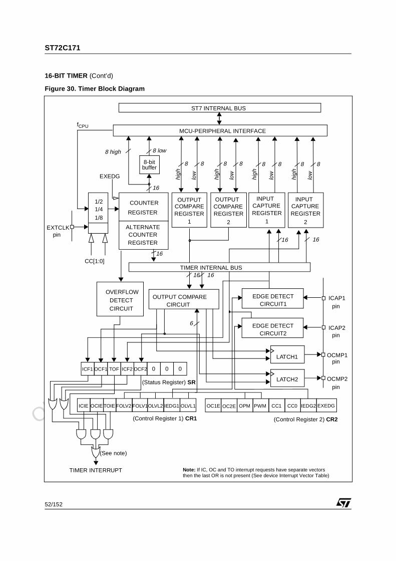
Obsolete Product(
s) - O
bsolete Product(
s)
ST72C171
52/152
16-BIT TIMER (Cont’d)
Figure 30. Timer Block Diagram
MCU-PERIPHERAL INTERFACE
COUNTERALTERNATE
OUTPUTCOMPAREREGISTER
OUTPUT COMPARE EDGE DETECTOVERFLOW
DETECT
CIRCUIT
1/21/4
1/8
8-bitbuffer
ST7 INTERNAL BUS
LATCH1 OCMP1
ICAP1
EXTCLK
fCPU
TIMER INTERRUPT
ICF2ICF1 000OCF2OCF1 TOF
PWMOC1E EXEDGIEDG2CC0CC1OC2E OPMFOLV2ICIE OLVL1IEDG1OLVL2FOLV1OCIE TOIE
ICAP2
LATCH2 OCMP2
8 8
8 low
16
8 high
16 16
16 16
(Control Register 1) CR1 (Control Register 2) CR2
(Status Register) SR
6
16
8 8 888 8
high
low
high
high
high
low
low
lowEXEDG
TIMER INTERNAL BUS
CIRCUIT1
EDGE DETECTCIRCUIT2
CIRCUIT
1
OUTPUTCOMPAREREGISTER
2
INPUTCAPTUREREGISTER
1
INPUTCAPTUREREGISTER
2
CC[1:0]
COUNTER
pin
pin
pin
pin
pin
REGISTER
REGISTER
Note: If IC, OC and TO interrupt requests have separate vectorsthen the last OR is not present (See device Interrupt Vector Table)
(See note)
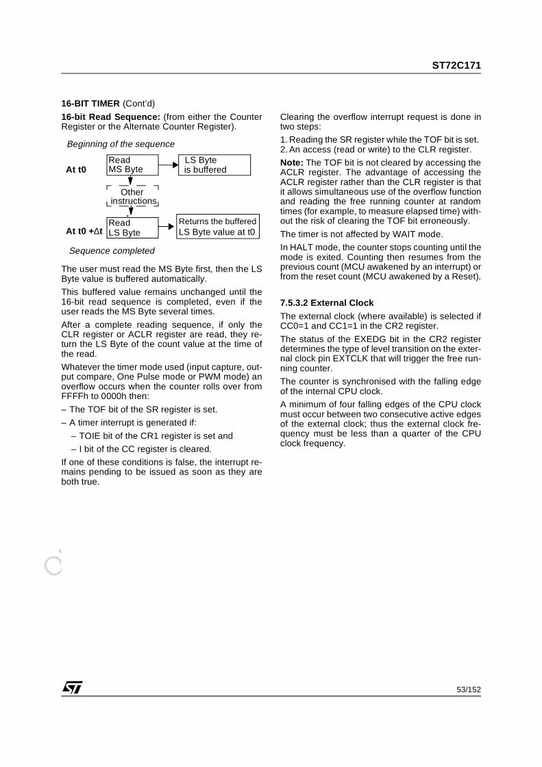
Obsolete Product(
s) - O
bsolete Product(
s)
ST72C171
53/152
16-BIT TIMER (Cont’d)
16-bit Read Sequence: (from either the CounterRegister or the Alternate Counter Register).
The user must read the MS Byte first, then the LSByte value is buffered automatically.
This buffered value remains unchanged until the16-bit read sequence is completed, even if theuser reads the MS Byte several times.
After a complete reading sequence, if only theCLR register or ACLR register are read, they re-turn the LS Byte of the count value at the time ofthe read.
Whatever the timer mode used (input capture, out-put compare, One Pulse mode or PWM mode) anoverflow occurs when the counter rolls over fromFFFFh to 0000h then:
– The TOF bit of the SR register is set.
– A timer interrupt is generated if:
– TOIE bit of the CR1 register is set and
– I bit of the CC register is cleared.
If one of these conditions is false, the interrupt re-mains pending to be issued as soon as they areboth true.
Clearing the overflow interrupt request is done intwo steps:
1. Reading the SR register while the TOF bit is set. 2. An access (read or write) to the CLR register.
Note: The TOF bit is not cleared by accessing theACLR register. The advantage of accessing theACLR register rather than the CLR register is thatit allows simultaneous use of the overflow functionand reading the free running counter at randomtimes (for example, to measure elapsed time) with-out the risk of clearing the TOF bit erroneously.
The timer is not affected by WAIT mode.
In HALT mode, the counter stops counting until themode is exited. Counting then resumes from theprevious count (MCU awakened by an interrupt) orfrom the reset count (MCU awakened by a Reset).
7.5.3.2 External Clock
The external clock (where available) is selected ifCC0=1 and CC1=1 in the CR2 register.
The status of the EXEDG bit in the CR2 registerdetermines the type of level transition on the exter-nal clock pin EXTCLK that will trigger the free run-ning counter.
The counter is synchronised with the falling edgeof the internal CPU clock.
A minimum of four falling edges of the CPU clockmust occur between two consecutive active edgesof the external clock; thus the external clock fre-quency must be less than a quarter of the CPUclock frequency.
is bufferedRead
At t0
Read Returns the bufferedLS Byte value at t0At t0 +∆t
Otherinstructions
Beginning of the sequence
Sequence completed
LS Byte
LS Byte
MS Byte
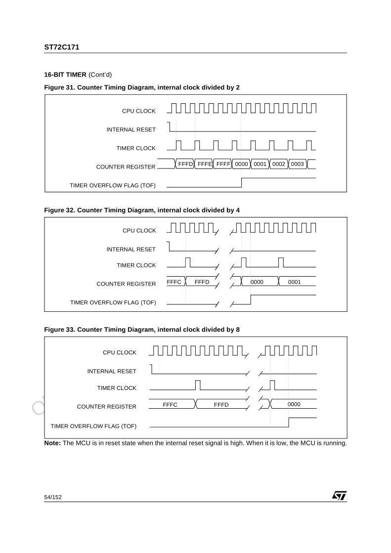
Obsolete Product(
s) - O
bsolete Product(
s)
ST72C171
54/152
16-BIT TIMER (Cont’d)
Figure 31. Counter Timing Diagram, internal clock divided by 2
Figure 32. Counter Timing Diagram, internal clock divided by 4
Figure 33. Counter Timing Diagram, internal clock divided by 8
Note: The MCU is in reset state when the internal reset signal is high. When it is low, the MCU is running.
CPU CLOCK
FFFD FFFE FFFF 0000 0001 0002 0003
INTERNAL RESET
TIMER CLOCK
COUNTER REGISTER
TIMER OVERFLOW FLAG (TOF)
FFFC FFFD 0000 0001
CPU CLOCK
INTERNAL RESET
TIMER CLOCK
COUNTER REGISTER
TIMER OVERFLOW FLAG (TOF)
CPU CLOCK
INTERNAL RESET
TIMER CLOCK
COUNTER REGISTER
TIMER OVERFLOW FLAG (TOF)
FFFC FFFD 0000
Obsolete Product(
s) - O
bsolete Product(
s)
ST72C171
55/152
16-BIT TIMER (Cont’d)
7.5.3.3 Input Capture
In this section, the index, i, may be 1 or 2 becausethere are 2 input capture functions in the 16-bittimer.
The two input capture 16-bit registers (IC1R andIC2R) are used to latch the value of the free run-ning counter after a transition is detected by theICAPi pin (see figure 5).
The ICiR register is a read-only register.
The active transition is software programmablethrough the IEDGi bit of Control Registers (CRi). Timing resolution is one count of the free runningcounter: (fCPU/CC[1:0]).
Procedure:To use the input capture function, select the fol-lowing in the CR2 register:
– Select the timer clock (CC[1:0]) (see Table 1).
– Select the edge of the active transition on theICAP2 pin with the IEDG2 bit (the ICAP2 pinmust be configured as a floating input).
And select the following in the CR1 register:
– Set the ICIE bit to generate an interrupt after aninput capture coming from either the ICAP1 pinor the ICAP2 pin
– Select the edge of the active transition on theICAP1 pin with the IEDG1 bit (the ICAP1pin mustbe configured as a floating input).
When an input capture occurs:
– The ICFi bit is set.
– The ICiR register contains the value of the freerunning counter on the active transition on theICAPi pin (see Figure 6).
– A timer interrupt is generated if the ICIE bit is setand the I bit is cleared in the CC register. Other-wise, the interrupt remains pending until bothconditions become true.
Clearing the Input Capture interrupt request (i.e.clearing the ICFi bit) is done in two steps:
1. Reading the SR register while the ICFi bit is set.
2. An access (read or write) to the ICiLR register.
Notes: 1. After reading the ICiHR register, the transfer of
input capture data is inhibited and ICFi willnever be set until the ICiLR register is alsoread.
2. The ICiR register contains the free runningcounter value which corresponds to the mostrecent input capture.
3. The 2 input capture functions can be usedtogether even if the timer also uses the 2 outputcompare functions.
4. In One Pulse mode and PWM mode only theinput capture 2 function can be used.
5. The alternate inputs (ICAP1 & ICAP2) arealways directly connected to the timer. So anytransitions on these pins activate the input cap-ture function.Moreover if one of the ICAPi pin is configuredas an input and the second one as an output,an interrupt can be generated if the user tog-gles the output pin and if the ICIE bit is set.This can be avoided if the input capture func-tion i is disabled by reading the ICiHR (see note1).
6. The TOF bit can be used with an interrupt inorder to measure events that exceed the timerrange (FFFFh).
MS Byte LS Byte
ICiR ICiHR ICiLR
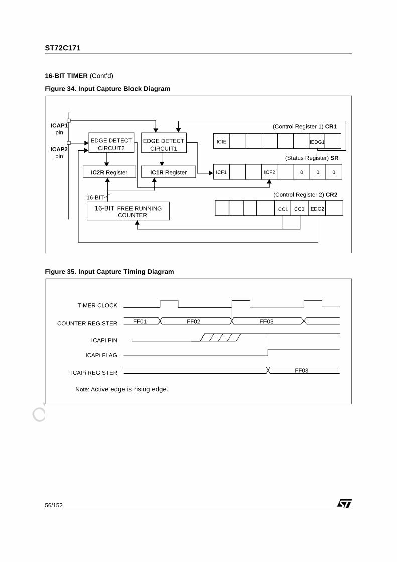
Obsolete Product(
s) - O
bsolete Product(
s)
ST72C171
56/152
16-BIT TIMER (Cont’d)
Figure 34. Input Capture Block Diagram
Figure 35. Input Capture Timing Diagram
ICIE
CC0CC116-BIT FREE RUNNINGCOUNTER
IEDG1
(Control Register 1) CR1
(Control Register 2) CR2
ICF2ICF1 000
(Status Register) SR
IEDG2
ICAP1
ICAP2
EDGE DETECTCIRCUIT2
16-BIT
IC1R RegisterIC2R Register
EDGE DETECTCIRCUIT1
pin
pin
FF01 FF02 FF03
FF03
TIMER CLOCK
COUNTER REGISTER
ICAPi PIN
ICAPi FLAG
ICAPi REGISTER
Note: Active edge is rising edge.
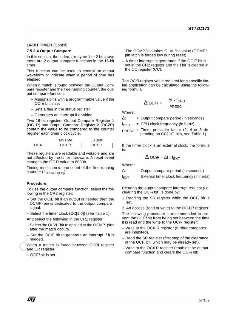
Obsolete Product(
s) - O
bsolete Product(
s)
ST72C171
57/152
16-BIT TIMER (Cont’d)
7.5.3.4 Output Compare
In this section, the index, i, may be 1 or 2 becausethere are 2 output compare functions in the 16-bittimer.
This function can be used to control an outputwaveform or indicate when a period of time haselapsed.
When a match is found between the Output Com-pare register and the free running counter, the out-put compare function:
– Assigns pins with a programmable value if theOCIE bit is set
– Sets a flag in the status register
– Generates an interrupt if enabled
Two 16-bit registers Output Compare Register 1(OC1R) and Output Compare Register 2 (OC2R)contain the value to be compared to the counterregister each timer clock cycle.
These registers are readable and writable and arenot affected by the timer hardware. A reset eventchanges the OCiR value to 8000h.
Timing resolution is one count of the free runningcounter: (fCPU/CC[1:0]).
Procedure:To use the output compare function, select the fol-lowing in the CR2 register:
– Set the OCiE bit if an output is needed then theOCMPi pin is dedicated to the output compare isignal.
– Select the timer clock (CC[1:0]) (see Table 1).
And select the following in the CR1 register:
– Select the OLVLi bit to applied to the OCMPi pinsafter the match occurs.
– Set the OCIE bit to generate an interrupt if it isneeded.
When a match is found between OCRi registerand CR register:
– OCFi bit is set.
– The OCMPi pin takes OLVLi bit value (OCMPi pin latch is forced low during reset).
– A timer interrupt is generated if the OCIE bit is set in the CR2 register and the I bit is cleared in the CC register (CC).
The OCiR register value required for a specific tim-ing application can be calculated using the follow-ing formula:
Where:
∆t = Output compare period (in seconds)
fCPU = CPU clock frequency (in hertz)
PRESC = Timer prescaler factor (2, 4 or 8 de-pending on CC[1:0] bits, see Table 1)
If the timer clock is an external clock, the formulais:
Where:
∆t = Output compare period (in seconds)
fEXT = External timer clock frequency (in hertz)
Clearing the output compare interrupt request (i.e.clearing the OCFi bit) is done by:
1. Reading the SR register while the OCFi bit isset.
2. An access (read or write) to the OCiLR register.
The following procedure is recommended to pre-vent the OCFi bit from being set between the timeit is read and the write to the OCiR register:
– Write to the OCiHR register (further compares are inhibited).
– Read the SR register (first step of the clearance of the OCFi bit, which may be already set).
– Write to the OCiLR register (enables the output compare function and clears the OCFi bit).
MS Byte LS Byte
OCiR OCiHR OCiLR
∆ OCiR =∆t * fCPU
PRESC
∆ OCiR = ∆t * fEXT
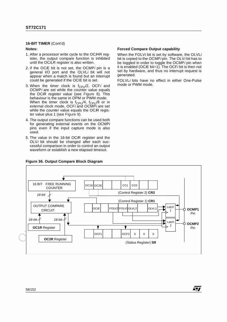
Obsolete Product(
s) - O
bsolete Product(
s)
ST72C171
58/152
16-BIT TIMER (Cont’d)
Notes: 1. After a processor write cycle to the OCiHR reg-
ister, the output compare function is inhibiteduntil the OCiLR register is also written.
2. If the OCiE bit is not set, the OCMPi pin is ageneral I/O port and the OLVLi bit will notappear when a match is found but an interruptcould be generated if the OCIE bit is set.
3. When the timer clock is fCPU/2, OCFi andOCMPi are set while the counter value equalsthe OCiR register value (see Figure 8). Thisbehaviour is the same in OPM or PWM mode.When the timer clock is fCPU/4, fCPU/8 or inexternal clock mode, OCFi and OCMPi are setwhile the counter value equals the OCiR regis-ter value plus 1 (see Figure 9).
4. The output compare functions can be used bothfor generating external events on the OCMPipins even if the input capture mode is alsoused.
5. The value in the 16-bit OCiR register and theOLVi bit should be changed after each suc-cessful comparison in order to control an outputwaveform or establish a new elapsed timeout.
Forced Compare Output capability
When the FOLVi bit is set by software, the OLVLibit is copied to the OCMPi pin. The OLVi bit has tobe toggled in order to toggle the OCMPi pin whenit is enabled (OCiE bit=1). The OCFi bit is then notset by hardware, and thus no interrupt request isgenerated.
FOLVLi bits have no effect in either One-Pulsemode or PWM mode.
Figure 36. Output Compare Block Diagram
OUTPUT COMPARE
16-bit
CIRCUIT
OC1R Register
16 BIT FREE RUNNINGCOUNTER
OC1E CC0CC1OC2E
OLVL1OLVL2OCIE
(Control Register 1) CR1
(Control Register 2) CR2
000OCF2OCF1
(Status Register) SR
16-bit
16-bit
OCMP1
OCMP2
Latch 1
Latch 2
OC2R Register
Pin
Pin
FOLV2 FOLV1
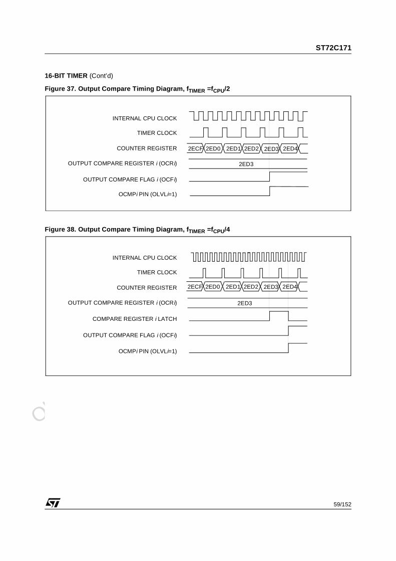
Obsolete Product(
s) - O
bsolete Product(
s)
ST72C171
59/152
16-BIT TIMER (Cont’d)
Figure 37. Output Compare Timing Diagram, fTIMER =fCPU/2
Figure 38. Output Compare Timing Diagram, fTIMER =fCPU/4
INTERNAL CPU CLOCK
TIMER CLOCK
COUNTER REGISTER
OUTPUT COMPARE REGISTER i (OCRi)
OUTPUT COMPARE FLAG i (OCFi)
OCMPi PIN (OLVLi=1)
2ED3
2ED0 2ED1 2ED2 2ED3 2ED42ECF
INTERNAL CPU CLOCK
TIMER CLOCK
COUNTER REGISTER
OUTPUT COMPARE REGISTER i (OCRi)
COMPARE REGISTER i LATCH
2ED3
2ED0 2ED1 2ED2 2ED3 2ED42ECF
OCMPi PIN (OLVLi=1)
OUTPUT COMPARE FLAG i (OCFi)
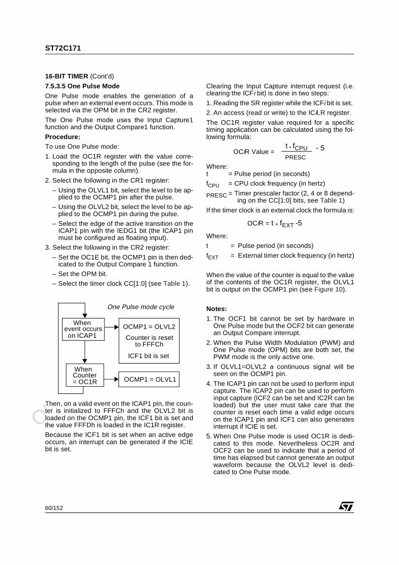
Obsolete Product(
s) - O
bsolete Product(
s)
ST72C171
60/152
16-BIT TIMER (Cont’d)
7.5.3.5 One Pulse Mode
One Pulse mode enables the generation of apulse when an external event occurs. This mode isselected via the OPM bit in the CR2 register.
The One Pulse mode uses the Input Capture1function and the Output Compare1 function.
Procedure:To use One Pulse mode:
1. Load the OC1R register with the value corre-sponding to the length of the pulse (see the for-mula in the opposite column).
2. Select the following in the CR1 register:
– Using the OLVL1 bit, select the level to be ap-plied to the OCMP1 pin after the pulse.
– Using the OLVL2 bit, select the level to be ap-plied to the OCMP1 pin during the pulse.
– Select the edge of the active transition on theICAP1 pin with the IEDG1 bit (the ICAP1 pinmust be configured as floating input).
3. Select the following in the CR2 register:
– Set the OC1E bit, the OCMP1 pin is then ded-icated to the Output Compare 1 function.
– Set the OPM bit.
– Select the timer clock CC[1:0] (see Table 1).
Then, on a valid event on the ICAP1 pin, the coun-ter is initialized to FFFCh and the OLVL2 bit isloaded on the OCMP1 pin, the ICF1 bit is set andthe value FFFDh is loaded in the IC1R register.
Because the ICF1 bit is set when an active edgeoccurs, an interrupt can be generated if the ICIEbit is set.
Clearing the Input Capture interrupt request (i.e.clearing the ICFi bit) is done in two steps:
1. Reading the SR register while the ICFi bit is set.
2. An access (read or write) to the ICiLR register.
The OC1R register value required for a specifictiming application can be calculated using the fol-lowing formula:
Where:t = Pulse period (in seconds)
fCPU = CPU clock frequency (in hertz)
PRESC = Timer prescaler factor (2, 4 or 8 depend-ing on the CC[1:0] bits, see Table 1)
If the timer clock is an external clock the formula is:
Where:
t = Pulse period (in seconds)
fEXT = External timer clock frequency (in hertz)
When the value of the counter is equal to the valueof the contents of the OC1R register, the OLVL1bit is output on the OCMP1 pin (see Figure 10).
Notes:
1. The OCF1 bit cannot be set by hardware inOne Pulse mode but the OCF2 bit can generatean Output Compare interrupt.
2. When the Pulse Width Modulation (PWM) andOne Pulse mode (OPM) bits are both set, thePWM mode is the only active one.
3. If OLVL1=OLVL2 a continuous signal will beseen on the OCMP1 pin.
4. The ICAP1 pin can not be used to perform inputcapture. The ICAP2 pin can be used to performinput capture (ICF2 can be set and IC2R can beloaded) but the user must take care that thecounter is reset each time a valid edge occurson the ICAP1 pin and ICF1 can also generatesinterrupt if ICIE is set.
5. When One Pulse mode is used OC1R is dedi-cated to this mode. Nevertheless OC2R andOCF2 can be used to indicate that a period oftime has elapsed but cannot generate an outputwaveform because the OLVL2 level is dedi-cated to One Pulse mode.
event occurs
Counter= OC1R OCMP1 = OLVL1
When
When
on ICAP1
One Pulse mode cycle
OCMP1 = OLVL2
Counter is resetto FFFCh
ICF1 bit is set
OCiR Value =t * fCPU
PRESC
- 5
OCiR = t * fEXT -5
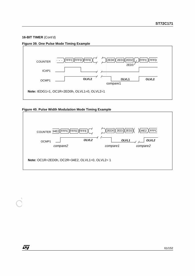
Obsolete Product(
s) - O
bsolete Product(
s)
ST72C171
61/152
16-BIT TIMER (Cont’d)
Figure 39. One Pulse Mode Timing Example
Figure 40. Pulse Width Modulation Mode Timing Example
COUNTER FFFC FFFD FFFE 2ED0 2ED1 2ED2
2ED3
FFFC FFFD
OLVL2 OLVL2OLVL1
ICAP1
OCMP1compare1
Note: IEDG1=1, OC1R=2ED0h, OLVL1=0, OLVL2=1
COUNTER 34E2 34E2 FFFC
OLVL2 OLVL2OLVL1OCMP1
compare2 compare1 compare2
Note: OC1R=2ED0h, OC2R=34E2, OLVL1=0, OLVL2= 1
FFFC FFFD FFFE 2ED0 2ED1 2ED2
Obsolete Product(
s) - O
bsolete Product(
s)
ST72C171
62/152
16-BIT TIMER (Cont’d)
7.5.3.6 Pulse Width Modulation Mode
Pulse Width Modulation (PWM) mode enables thegeneration of a signal with a frequency and pulselength determined by the value of the OC1R andOC2R registers.
The Pulse Width Modulation mode uses the com-plete Output Compare 1 function plus the OC2Rregister, and so these functions cannot be usedwhen the PWM mode is activated.
ProcedureTo use Pulse Width Modulation mode:
1. Load the OC2R register with the value corre-sponding to the period of the signal using theformula in the opposite column.
2. Load the OC1R register with the value corre-sponding to the period of the pulse if OLVL1=0and OLVL2=1, using the formula in the oppo-site column.
3. Select the following in the CR1 register:
– Using the OLVL1 bit, select the level to be ap-plied to the OCMP1 pin after a successfulcomparison with OC1R register.
– Using the OLVL2 bit, select the level to be ap-plied to the OCMP1 pin after a successfulcomparison with OC2R register.
4. Select the following in the CR2 register:
– Set OC1E bit: the OCMP1 pin is then dedicat-ed to the output compare 1 function.
– Set the PWM bit.
– Select the timer clock (CC[1:0]) (see Table 1).
If OLVL1=1 and OLVL2=0, the length of the posi-tive pulse is the difference between the OC2R andOC1R registers.
If OLVL1=OLVL2 a continuous signal will be seenon the OCMP1 pin.
The OCiR register value required for a specific tim-ing application can be calculated using the follow-ing formula:
Where:t = Signal or pulse period (in seconds)
fCPU = CPU clock frequency (in hertz)
PRESC = Timer prescaler factor (2, 4 or 8 depend-ing on CC[1:0] bits, see Table 1)
If the timer clock is an external clock the formula is:
Where:
t = Signal or pulse period (in seconds)
fEXT = External timer clock frequency (in hertz)
The Output Compare 2 event causes the counterto be initialized to FFFCh (See Figure 11)
Notes: 1. After a write instruction to the OCiHR register,
the output compare function is inhibited until theOCiLR register is also written.
2. The OCF1 and OCF2 bits cannot be set byhardware in PWM mode, therefore the OutputCompare interrupt is inhibited.
3. The ICF1 bit is set by hardware when the coun-ter reaches the OC2R value and can produce atimer interrupt if the ICIE bit is set and the I bit iscleared.
4. In PWM mode the ICAP1 pin can not be usedto perform input capture because it is discon-nected from the timer. The ICAP2 pin can beused to perform input capture (ICF2 can be setand IC2R can be loaded) but the user musttake care that the counter is reset after eachperiod and ICF1 can also generate an interruptif ICIE is set.
5. When the Pulse Width Modulation (PWM) andOne Pulse mode (OPM) bits are both set, thePWM mode is the only active one.
Counter
OCMP1 = OLVL2Counter= OC2R
OCMP1 = OLVL1
When
When
= OC1R
Pulse Width Modulation cycle
Counter is resetto FFFCh
ICF1 bit is set
OCiR Value =t * fCPU
PRESC
- 5
OCiR = t * fEXT -5
Obsolete Product(
s) - O
bsolete Product(
s)
ST72C171
63/152
16-BIT TIMER (Cont’d)
7.5.4 Low Power Modes
7.5.5 Interrupts
Note: The 16-bit Timer interrupt events are connected to the same interrupt vector (see Interrupts chap-ter). These events generate an interrupt if the corresponding Enable Control Bit is set and the interruptmask in the CC register is reset (RIM instruction).
7.5.6 Summary of Timer modes
1) See note 4 in Section 0.1.3.5 One Pulse Mode2) See note 5 in Section 0.1.3.5 One Pulse Mode3) See note 4 in Section 0.1.3.6 Pulse Width Modulation Mode
Mode Description
WAITNo effect on 16-bit Timer. Timer interrupts cause the device to exit from WAIT mode.
HALT
16-bit Timer registers are frozen.
In HALT mode, the counter stops counting until Halt mode is exited. Counting resumes from the previous count when the MCU is woken up by an interrupt with “exit from HALT mode” capability or from the counter reset value when the MCU is woken up by a RESET.
If an input capture event occurs on the ICAPi pin, the input capture detection circuitry is armed. Consequent-ly, when the MCU is woken up by an interrupt with “exit from HALT mode” capability, the ICFi bit is set, and the counter value present when exiting from HALT mode is captured into the ICiR register.
Interrupt EventEventFlag
Enable Control
Bit
Exit fromWait
Exit from Halt
Input Capture 1 event/Counter reset in PWM mode ICF1ICIE
Yes No
Input Capture 2 event ICF2 Yes No
Output Compare 1 event (not available in PWM mode) OCF1OCIE
Yes No
Output Compare 2 event (not available in PWM mode) OCF2 Yes No
Timer Overflow event TOF TOIE Yes No
MODESAVAILABLE RESOURCES
Input Capture 1 Input Capture 2 Output Compare 1 Output Compare 2Input Capture (1 and/or 2) Yes Yes Yes Yes
Output Compare (1 and/or 2) Yes Yes Yes Yes
One Pulse mode No Not Recommended1) No Partially 2)
PWM Mode No Not Recommended3) No No
Obsolete Product(
s) - O
bsolete Product(
s)
ST72C171
64/152
16-BIT TIMER (Cont’d)
7.5.7 Register Description
Each Timer is associated with three control andstatus registers, and with six pairs of data registers(16-bit values) relating to the two input captures,the two output compares, the counter and the al-ternate counter.
CONTROL REGISTER 1 (CR1)
Read/Write
Reset Value: 0000 0000 (00h)
Bit 7 = ICIE Input Capture Interrupt Enable.0: Interrupt is inhibited.1: A timer interrupt is generated whenever the
ICF1 or ICF2 bit of the SR register is set.
Bit 6 = OCIE Output Compare Interrupt Enable.0: Interrupt is inhibited.1: A timer interrupt is generated whenever the
OCF1 or OCF2 bit of the SR register is set.
Bit 5 = TOIE Timer Overflow Interrupt Enable.0: Interrupt is inhibited.1: A timer interrupt is enabled whenever the TOF
bit of the SR register is set.
Bit 4 = FOLV2 Forced Output Compare 2.This bit is set and cleared by software.0: No effect on the OCMP2 pin.1: Forces the OLVL2 bit to be copied to the
OCMP2 pin, if the OC2E bit is set and even ifthere is no successful comparison.
Bit 3 = FOLV1 Forced Output Compare 1.This bit is set and cleared by software.0: No effect on the OCMP1 pin.1: Forces OLVL1 to be copied to the OCMP1 pin, if
the OC1E bit is set and even if there is no suc-cessful comparison.
Bit 2 = OLVL2 Output Level 2.This bit is copied to the OCMP2 pin whenever asuccessful comparison occurs with the OC2R reg-ister and OCxE is set in the CR2 register. This val-ue is copied to the OCMP1 pin in One Pulse modeand Pulse Width Modulation mode.
Bit 1 = IEDG1 Input Edge 1.This bit determines which type of level transitionon the ICAP1 pin will trigger the capture.0: A falling edge triggers the capture.1: A rising edge triggers the capture.
Bit 0 = OLVL1 Output Level 1.The OLVL1 bit is copied to the OCMP1 pin when-ever a successful comparison occurs with theOC1R register and the OC1E bit is set in the CR2register.
7 0
ICIE OCIE TOIE FOLV2 FOLV1 OLVL2 IEDG1 OLVL1
Obsolete Product(
s) - O
bsolete Product(
s)
ST72C171
65/152
16-BIT TIMER (Cont’d)
CONTROL REGISTER 2 (CR2)
Read/Write
Reset Value: 0000 0000 (00h)
Bit 7 = OC1E Output Compare 1 Pin Enable.This bit is used only to output the signal from thetimer on the OCMP1 pin (OLV1 in Output Com-pare mode, both OLV1 and OLV2 in PWM andone-pulse mode). Whatever the value of the OC1Ebit, the internal Output Compare 1 function of thetimer remains active.0: OCMP1 pin alternate function disabled (I/O pin
free for general-purpose I/O).1: OCMP1 pin alternate function enabled.
Bit 6 = OC2E Output Compare 2 Pin Enable.This bit is used only to output the signal from thetimer on the OCMP2 pin (OLV2 in Output Com-pare mode). Whatever the value of the OC2E bit,the internal Output Compare 2 function of the timerremains active.0: OCMP2 pin alternate function disabled (I/O pin
free for general-purpose I/O).1: OCMP2 pin alternate function enabled.
Bit 5 = OPM One Pulse mode.0: One Pulse mode is not active.1: One Pulse mode is active, the ICAP1 pin can be
used to trigger one pulse on the OCMP1 pin; theactive transition is given by the IEDG1 bit. Thelength of the generated pulse depends on thecontents of the OC1R register.
Bit 4 = PWM Pulse Width Modulation.0: PWM mode is not active.1: PWM mode is active, the OCMP1 pin outputs a
programmable cyclic signal; the length of thepulse depends on the value of OC1R register;the period depends on the value of OC2R regis-ter.
Bits 3:2 = CC[1:0] Clock Control.
The timer clock mode depends on these bits:
Table 14. Clock Control Bits
Note: If the external clock pin is not available, pro-gramming the external clock configuration stopsthe counter.
Bit 1 = IEDG2 Input Edge 2.This bit determines which type of level transitionon the ICAP2 pin will trigger the capture.0: A falling edge triggers the capture.1: A rising edge triggers the capture.
Bit 0 = EXEDG External Clock Edge.This bit determines which type of level transitionon the external clock pin (EXTCLK) will trigger thecounter register. 0: A falling edge triggers the counter register.1: A rising edge triggers the counter register.
7 0
OC1E OC2E OPM PWM CC1 CC0 IEDG2 EXEDG
Timer Clock CC1 CC0fCPU / 4 0 0fCPU / 2 0 1fCPU / 8 1 0
External Clock (where available)
1 1
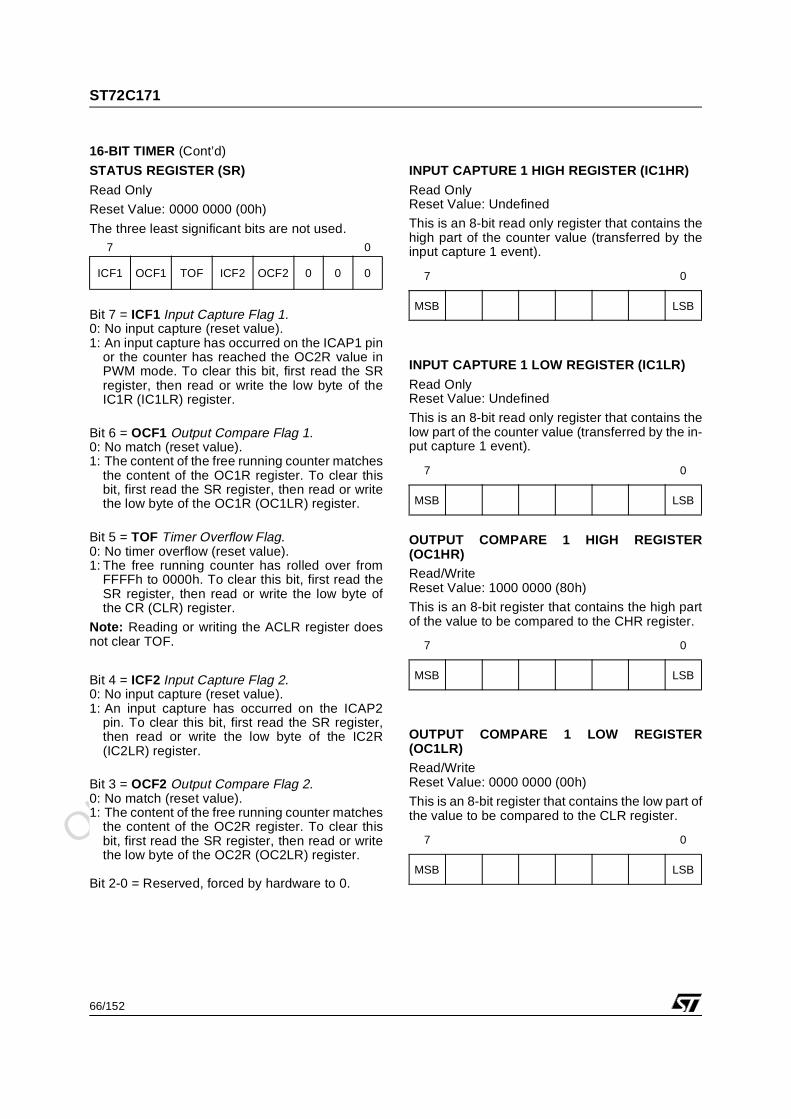
Obsolete Product(
s) - O
bsolete Product(
s)
ST72C171
66/152
16-BIT TIMER (Cont’d)
STATUS REGISTER (SR)
Read Only
Reset Value: 0000 0000 (00h)
The three least significant bits are not used.
Bit 7 = ICF1 Input Capture Flag 1.0: No input capture (reset value).1: An input capture has occurred on the ICAP1 pin
or the counter has reached the OC2R value inPWM mode. To clear this bit, first read the SRregister, then read or write the low byte of theIC1R (IC1LR) register.
Bit 6 = OCF1 Output Compare Flag 1.0: No match (reset value).1: The content of the free running counter matches
the content of the OC1R register. To clear thisbit, first read the SR register, then read or writethe low byte of the OC1R (OC1LR) register.
Bit 5 = TOF Timer Overflow Flag.0: No timer overflow (reset value).1: The free running counter has rolled over from
FFFFh to 0000h. To clear this bit, first read theSR register, then read or write the low byte ofthe CR (CLR) register.
Note: Reading or writing the ACLR register doesnot clear TOF.
Bit 4 = ICF2 Input Capture Flag 2.0: No input capture (reset value).1: An input capture has occurred on the ICAP2
pin. To clear this bit, first read the SR register,then read or write the low byte of the IC2R(IC2LR) register.
Bit 3 = OCF2 Output Compare Flag 2.0: No match (reset value).1: The content of the free running counter matches
the content of the OC2R register. To clear thisbit, first read the SR register, then read or writethe low byte of the OC2R (OC2LR) register.
Bit 2-0 = Reserved, forced by hardware to 0.
INPUT CAPTURE 1 HIGH REGISTER (IC1HR)
Read OnlyReset Value: Undefined
This is an 8-bit read only register that contains thehigh part of the counter value (transferred by theinput capture 1 event).
INPUT CAPTURE 1 LOW REGISTER (IC1LR)
Read OnlyReset Value: Undefined
This is an 8-bit read only register that contains thelow part of the counter value (transferred by the in-put capture 1 event).
OUTPUT COMPARE 1 HIGH REGISTER(OC1HR)Read/WriteReset Value: 1000 0000 (80h)
This is an 8-bit register that contains the high partof the value to be compared to the CHR register.
OUTPUT COMPARE 1 LOW REGISTER(OC1LR)Read/WriteReset Value: 0000 0000 (00h)
This is an 8-bit register that contains the low part ofthe value to be compared to the CLR register.
7 0
ICF1 OCF1 TOF ICF2 OCF2 0 0 0 7 0
MSB LSB
7 0
MSB LSB
7 0
MSB LSB
7 0
MSB LSB
Obsolete Product(
s) - O
bsolete Product(
s)
ST72C171
67/152
16-BIT TIMER (Cont’d)
OUTPUT COMPARE 2 HIGH REGISTER(OC2HR)
Read/WriteReset Value: 1000 0000 (80h)
This is an 8-bit register that contains the high partof the value to be compared to the CHR register.
OUTPUT COMPARE 2 LOW REGISTER(OC2LR)
Read/WriteReset Value: 0000 0000 (00h)
This is an 8-bit register that contains the low part ofthe value to be compared to the CLR register.
COUNTER HIGH REGISTER (CHR)
Read OnlyReset Value: 1111 1111 (FFh)
This is an 8-bit register that contains the high partof the counter value.
COUNTER LOW REGISTER (CLR)
Read OnlyReset Value: 1111 1100 (FCh)
This is an 8-bit register that contains the low part ofthe counter value. A write to this register resets thecounter. An access to this register after accessingthe SR register clears the TOF bit.
ALTERNATE COUNTER HIGH REGISTER(ACHR)
Read OnlyReset Value: 1111 1111 (FFh)
This is an 8-bit register that contains the high partof the counter value.
ALTERNATE COUNTER LOW REGISTER(ACLR)
Read OnlyReset Value: 1111 1100 (FCh)
This is an 8-bit register that contains the low part ofthe counter value. A write to this register resets thecounter. An access to this register after an accessto SR register does not clear the TOF bit in SRregister.
INPUT CAPTURE 2 HIGH REGISTER (IC2HR)
Read OnlyReset Value: Undefined
This is an 8-bit read only register that contains thehigh part of the counter value (transferred by theInput Capture 2 event).
INPUT CAPTURE 2 LOW REGISTER (IC2LR)
Read OnlyReset Value: Undefined
This is an 8-bit read only register that contains thelow part of the counter value (transferred by the In-put Capture 2 event).
7 0
MSB LSB
7 0
MSB LSB
7 0
MSB LSB
7 0
MSB LSB
7 0
MSB LSB
7 0
MSB LSB
7 0
MSB LSB
7 0
MSB LSB
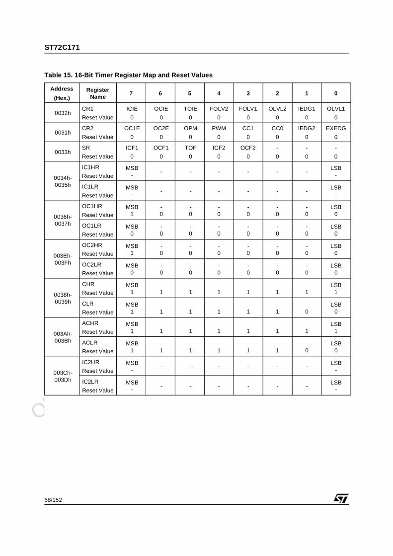
Obsolete Product(
s) - O
bsolete Product(
s)
ST72C171
68/152
Table 15. 16-Bit Timer Register Map and Reset Values
Address
(Hex.)Register
Name7 6 5 4 3 2 1 0
0032hCR1
Reset Value
ICIE
0
OCIE
0
TOIE
0
FOLV2
0
FOLV1
0
OLVL2
0
IEDG1
0
OLVL1
0
0031hCR2
Reset Value
OC1E
0
OC2E
0
OPM
0
PWM
0
CC1
0
CC0
0
IEDG2
0
EXEDG
0
0033hSR
Reset Value
ICF1
0
OCF1
0
TOF
0
ICF2
0
OCF2
0
-
0
-
0
-
0
0034h-0035h
IC1HR
Reset ValueMSB
-- - - - - -
LSB-
IC1LR
Reset ValueMSB
-- - - - - -
LSB-
0036h-0037h
OC1HR
Reset ValueMSB
1-0
-0
-0
-0
-0
-0
LSB0
OC1LR
Reset ValueMSB
0-0
-0
-0
-0
-0
-0
LSB0
003Eh-003Fh
OC2HR
Reset ValueMSB
1-0
-0
-0
-0
-0
-0
LSB0
OC2LR
Reset ValueMSB
0-0
-0
-0
-0
-0
-0
LSB0
0038h-0039h
CHR
Reset ValueMSB
1 1 1 1 1 1 1LSB
1
CLR
Reset ValueMSB
1 1 1 1 1 1 0LSB
0
003Ah-003Bh
ACHR
Reset ValueMSB
1 1 1 1 1 1 1LSB
1
ACLR
Reset ValueMSB
1 1 1 1 1 1 0LSB
0
003Ch-003Dh
IC2HR
Reset ValueMSB
-- - - - - -
LSB-
IC2LR
Reset ValueMSB
-- - - - - -
LSB-
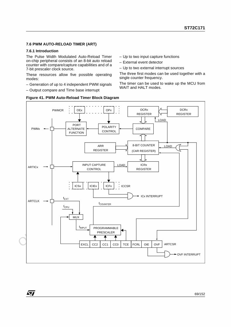
Obsolete Product(
s) - O
bsolete Product(
s)
ST72C171
69/152
7.6 PWM AUTO-RELOAD TIMER (ART)
7.6.1 Introduction
The Pulse Width Modulated Auto-Reload Timeron-chip peripheral consists of an 8-bit auto reloadcounter with compare/capture capabilities and of a7-bit prescaler clock source.
These resources allow five possible operatingmodes:
– Generation of up to 4 independent PWM signals
– Output compare and Time base interrupt
– Up to two input capture functions
– External event detector
– Up to two external interrupt sources
The three first modes can be used together with asingle counter frequency.
The timer can be used to wake up the MCU fromWAIT and HALT modes.
Figure 41. PWM Auto-Reload Timer Block Diagram
OVF INTERRUPT
EXCL CC2 CC1 CC0 TCE FCRL OIE OVF ARTCSR
fINPUT
PWMxPORT
FUNCTIONALTERNATE
OCRx
COMPARE
REGISTER
PROGRAMMABLE
PRESCALER
8-BIT COUNTER
(CAR REGISTER)
ARR
REGISTER
ICRx
REGISTER
LOAD
OPx
POLARITY
CONTROL
OExPWMCR
MUX
fCPU
DCRx
REGISTER
LOAD
fCOUNTERARTCLK
fEXT
ARTICx
ICFxICSx ICCSR
LOAD
ICx INTERRUPT
ICIEx
INPUT CAPTURE
CONTROL
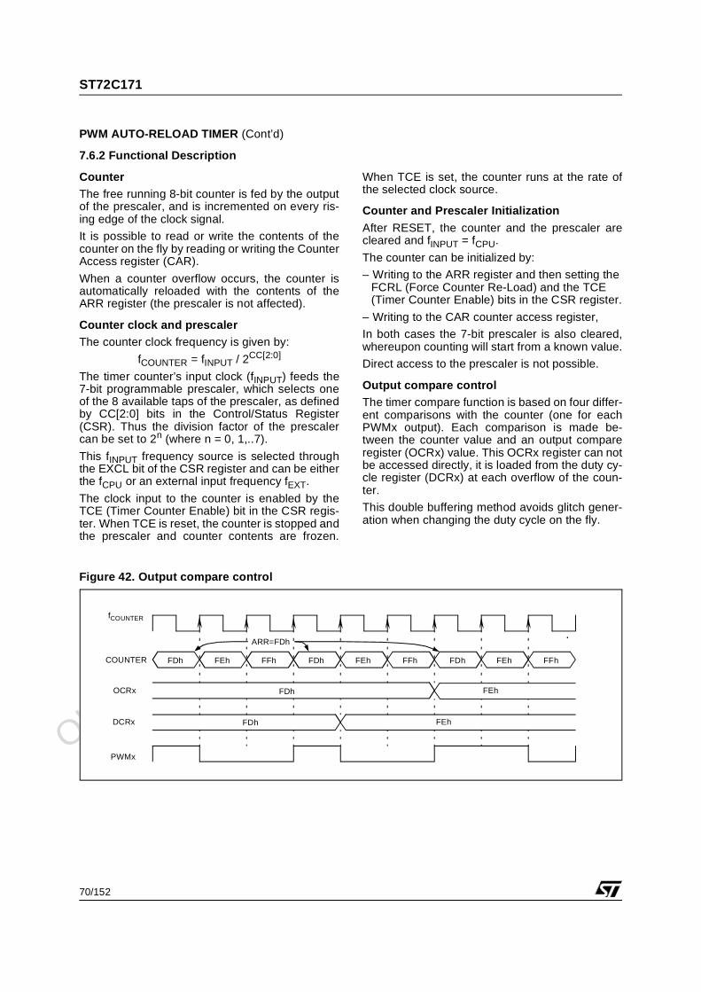
Obsolete Product(
s) - O
bsolete Product(
s)
ST72C171
70/152
PWM AUTO-RELOAD TIMER (Cont’d)
7.6.2 Functional Description
CounterThe free running 8-bit counter is fed by the outputof the prescaler, and is incremented on every ris-ing edge of the clock signal.
It is possible to read or write the contents of thecounter on the fly by reading or writing the CounterAccess register (CAR).
When a counter overflow occurs, the counter isautomatically reloaded with the contents of theARR register (the prescaler is not affected).
Counter clock and prescalerThe counter clock frequency is given by:
fCOUNTER = fINPUT / 2CC[2:0]
The timer counter’s input clock (fINPUT) feeds the7-bit programmable prescaler, which selects oneof the 8 available taps of the prescaler, as definedby CC[2:0] bits in the Control/Status Register(CSR). Thus the division factor of the prescalercan be set to 2n (where n = 0, 1,..7).
This fINPUT frequency source is selected throughthe EXCL bit of the CSR register and can be eitherthe fCPU or an external input frequency fEXT.
The clock input to the counter is enabled by theTCE (Timer Counter Enable) bit in the CSR regis-ter. When TCE is reset, the counter is stopped andthe prescaler and counter contents are frozen.
When TCE is set, the counter runs at the rate ofthe selected clock source.
Counter and Prescaler Initialization
After RESET, the counter and the prescaler arecleared and fINPUT = fCPU.
The counter can be initialized by:
– Writing to the ARR register and then setting the FCRL (Force Counter Re-Load) and the TCE (Timer Counter Enable) bits in the CSR register.
– Writing to the CAR counter access register,
In both cases the 7-bit prescaler is also cleared,whereupon counting will start from a known value.
Direct access to the prescaler is not possible.
Output compare controlThe timer compare function is based on four differ-ent comparisons with the counter (one for eachPWMx output). Each comparison is made be-tween the counter value and an output compareregister (OCRx) value. This OCRx register can notbe accessed directly, it is loaded from the duty cy-cle register (DCRx) at each overflow of the coun-ter.
This double buffering method avoids glitch gener-ation when changing the duty cycle on the fly.
Figure 42. Output compare control
COUNTER FDh FEh FFh FDh FEh FFh FDh FEh
ARR=FDh
fCOUNTER
OCRx
DCRx FDh FEh
FDh FEh
FFh
PWMx
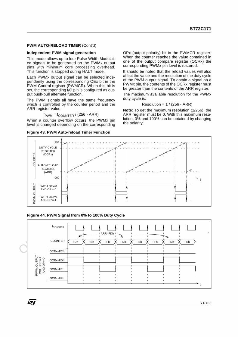
Obsolete Product(
s) - O
bsolete Product(
s)
ST72C171
71/152
PWM AUTO-RELOAD TIMER (Cont’d)
Independent PWM signal generation
This mode allows up to four Pulse Width Modulat-ed signals to be generated on the PWMx outputpins with minimum core processing overhead.This function is stopped during HALT mode.
Each PWMx output signal can be selected inde-pendently using the corresponding OEx bit in thePWM Control register (PWMCR). When this bit isset, the corresponding I/O pin is configured as out-put push-pull alternate function.
The PWM signals all have the same frequencywhich is controlled by the counter period and theARR register value.
fPWM = fCOUNTER / (256 - ARR)
When a counter overflow occurs, the PWMx pinlevel is changed depending on the corresponding
OPx (output polarity) bit in the PWMCR register.When the counter reaches the value contained inone of the output compare register (OCRx) thecorresponding PWMx pin level is restored.
It should be noted that the reload values will alsoaffect the value and the resolution of the duty cycleof the PWM output signal. To obtain a signal on aPWMx pin, the contents of the OCRx register mustbe greater than the contents of the ARR register.
The maximum available resolution for the PWMxduty cycle is:
Resolution = 1 / (256 - ARR)
Note: To get the maximum resolution (1/256), theARR register must be 0. With this maximum reso-lution, 0% and 100% can be obtained by changingthe polarity.
Figure 43. PWM Auto-reload Timer Function
Figure 44. PWM Signal from 0% to 100% Duty Cycle
DUTY CYCLEREGISTER
AUTO-RELOADREGISTER
PW
Mx
OU
TP
UT
t
255
000
WITH OEx=1AND OPx=0
(ARR)
(DCRx)
WITH OEx=1AND OPx=1
CO
UN
TE
R
COUNTER
PW
Mx
OU
TP
UT
t
WIT
H O
Ex=
1A
ND
OP
x=0
FDh FEh FFh FDh FEh FFh FDh FEh
OCRx=FCh
OCRx=FDh
OCRx=FEh
OCRx=FFh
ARR=FDh
fCOUNTER
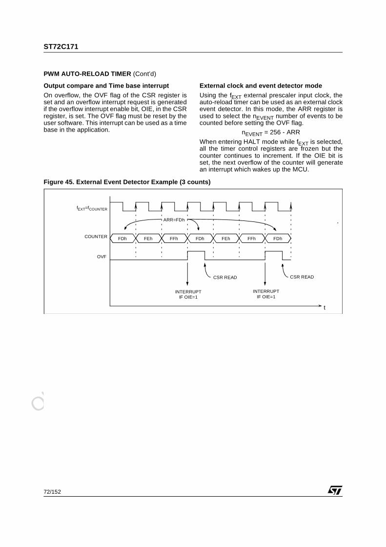
Obsolete Product(
s) - O
bsolete Product(
s)
ST72C171
72/152
PWM AUTO-RELOAD TIMER (Cont’d)
Output compare and Time base interrupt
On overflow, the OVF flag of the CSR register isset and an overflow interrupt request is generatedif the overflow interrupt enable bit, OIE, in the CSRregister, is set. The OVF flag must be reset by theuser software. This interrupt can be used as a timebase in the application.
External clock and event detector mode
Using the fEXT external prescaler input clock, theauto-reload timer can be used as an external clockevent detector. In this mode, the ARR register isused to select the nEVENT number of events to becounted before setting the OVF flag.
nEVENT = 256 - ARR
When entering HALT mode while fEXT is selected,all the timer control registers are frozen but thecounter continues to increment. If the OIE bit isset, the next overflow of the counter will generatean interrupt which wakes up the MCU.
Figure 45. External Event Detector Example (3 counts)
COUNTER
t
FDh FEh FFh FDh
OVF
CSR READ
INTERRUPT
ARR=FDh
fEXT=fCOUNTER
FEh FFh FDh
IF OIE=1INTERRUPT
IF OIE=1
CSR READ
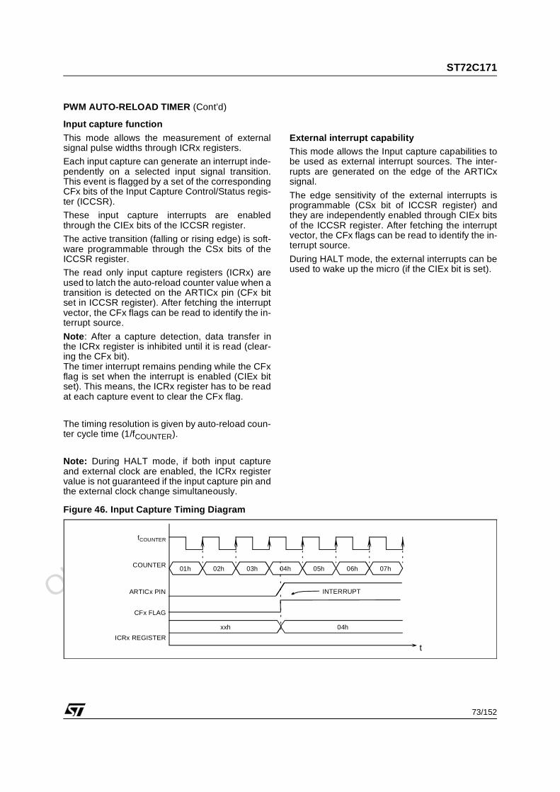
Obsolete Product(
s) - O
bsolete Product(
s)
ST72C171
73/152
PWM AUTO-RELOAD TIMER (Cont’d)
Input capture function
This mode allows the measurement of externalsignal pulse widths through ICRx registers.
Each input capture can generate an interrupt inde-pendently on a selected input signal transition.This event is flagged by a set of the correspondingCFx bits of the Input Capture Control/Status regis-ter (ICCSR).
These input capture interrupts are enabledthrough the CIEx bits of the ICCSR register.
The active transition (falling or rising edge) is soft-ware programmable through the CSx bits of theICCSR register.
The read only input capture registers (ICRx) areused to latch the auto-reload counter value when atransition is detected on the ARTICx pin (CFx bitset in ICCSR register). After fetching the interruptvector, the CFx flags can be read to identify the in-terrupt source.
Note: After a capture detection, data transfer inthe ICRx register is inhibited until it is read (clear-ing the CFx bit).The timer interrupt remains pending while the CFxflag is set when the interrupt is enabled (CIEx bitset). This means, the ICRx register has to be readat each capture event to clear the CFx flag.
The timing resolution is given by auto-reload coun-ter cycle time (1/fCOUNTER).
Note: During HALT mode, if both input captureand external clock are enabled, the ICRx registervalue is not guaranteed if the input capture pin andthe external clock change simultaneously.
External interrupt capabilityThis mode allows the Input capture capabilities tobe used as external interrupt sources. The inter-rupts are generated on the edge of the ARTICxsignal.
The edge sensitivity of the external interrupts isprogrammable (CSx bit of ICCSR register) andthey are independently enabled through CIEx bitsof the ICCSR register. After fetching the interruptvector, the CFx flags can be read to identify the in-terrupt source.
During HALT mode, the external interrupts can beused to wake up the micro (if the CIEx bit is set).
Figure 46. Input Capture Timing Diagram
04hCOUNTER
t
01h
fCOUNTER
xxh
02h 03h 05h 06h 07h
04h
ARTICx PIN
CFx FLAG
ICRx REGISTER
INTERRUPT
Obsolete Product(
s) - O
bsolete Product(
s)
ST72C171
74/152
PWM AUTO-RELOAD TIMER (Cont’d)
7.6.3 Register Description
CONTROL / STATUS REGISTER (CSR)
Read/Write
Reset Value: 0000 0000 (00h)
Bit 7 = EXCL External ClockThis bit is set and cleared by software. It selects theinput clock for the 7-bit prescaler.0: CPU clock.1: External clock.
Bit 6:4 = CC[2:0] Counter Clock ControlThese bits are set and cleared by software. Theydetermine the prescaler division ratio from fINPUT.
Bit 3 = TCE Timer Counter EnableThis bit is set and cleared by software. It puts thetimer in the lowest power consumption mode.0: Counter stopped (prescaler and counter frozen).1: Counter running.
Bit 2 = FCRL Force Counter Re-LoadThis bit is write-only and any attempt to read it willyield a logical zero. When set, it causes the contentsof ARR register to be loaded into the counter, andthe content of the prescaler register to be cleared inorder to initialize the timer before starting to count.
Bit 1 = OIE Overflow Interrupt EnableThis bit is set and cleared by software. It allows toenable/disable the interrupt which is generatedwhen the OVF bit is set.0: Overflow Interrupt disable.1: Overflow Interrupt enable.
Bit 0 = OVF Overflow FlagThis bit is set by hardware and cleared by softwarereading the CSR register. It indicates the transitionof the counter from FFh to the ARR value.
0: New transition not yet reached1: Transition reached
COUNTER ACCESS REGISTER (CAR)
Read/Write
Reset Value: 0000 0000 (00h)
Bit 7:0 = CA[7:0] Counter Access DataThese bits can be set and cleared either by hard-ware or by software. The CAR register is used toread or write the auto-reload counter “on the fly”(while it is counting).
AUTO-RELOAD REGISTER (ARR)Read/Write
Reset Value: 0000 0000 (00h)
Bit 7:0 = AR[7:0] Counter Auto-Reload Data
These bits are set and cleared by software. Theyare used to hold the auto-reload value which is au-tomatically loaded in the counter when an overflowoccurs. At the same time, the PWM output levelsare changed according to the corresponding OPxbit in the PWMCR register.
This register has two PWM management func-tions:
– Adjusting the PWM frequency– Setting the PWM duty cycle resolution
PWM Frequency vs. Resolution:
7 0
EXCL CC2 CC1 CC0 TCE FCRL OIE OVF
fCOUNTER With fINPUT=8 MHz CC2 CC1 CC0fINPUT
fINPUT / 2fINPUT / 4fINPUT / 8fINPUT / 16fINPUT / 32fINPUT / 64fINPUT / 128
8 MHz4 MHz2 MHz1 MHz
500 KHz250 KHz125 KHz62.5 KHz
00001111
00110011
01010101
7 0
CA7 CA6 CA5 CA4 CA3 CA2 CA1 CA0
7 0
AR7 AR6 AR5 AR4 AR3 AR2 AR1 AR0
ARR value ResolutionfPWM
Min Max0 8-bit ~0.244-KHz 31.25-KHz
[ 0..127 ] > 7-bit ~0.244-KHz 62.5-KHz
[ 128..191 ] > 6-bit ~0.488-KHz 125-KHz
[ 192..223 ] > 5-bit ~0.977-KHz 250-KHz
[ 224..239 ] > 4-bit ~1.953-KHz 500-KHz
Obsolete Product(
s) - O
bsolete Product(
s)
ST72C171
75/152
PWM AUTO-RELOAD TIMER (Cont’d)
PWM CONTROL REGISTER (PWMCR)
Read/Write
Reset Value: 0000 0000 (00h)
Bit 7:6 = Reserved.
Bit 5:4 = OE[1:0] PWM Output EnableThese bits are set and cleared by software. Theyenable or disable the PWM output channels inde-pendently acting on the corresponding I/O pin.0: PWM output disabled.1: PWM output enabled.
Bit 3:2 = Reserved.
Bit 1:0 = OP[1:0] PWM Output PolarityThese bits are set and cleared by software. Theyindependently select the polarity of the two PWMoutput signals.
Note: When an OPx bit is modified, the PWMx out-put signal polarity is immediately reversed.
DUTY CYCLE REGISTERS (DCRx)
Read/Write
Reset Value: 0000 0000 (00h)
Bit 7:0 = DC[7:0] Duty Cycle Data
These bits are set and cleared by software.
A DCRx register is associated with the OCRx reg-ister of each PWM channel to determine the sec-ond edge location of the PWM signal (the firstedge location is common to all channels and givenby the ARR register). These DCR registers allowthe duty cycle to be set independently for eachPWM channel.
7 0
0 0 OE1 OE0 0 0 OP1 OP0
PWMx output levelOPx
Counter <= OCRx Counter > OCRx1 0 0
0 1 1
7 0
DC7 DC6 DC5 DC4 DC3 DC2 DC1 DC0
Obsolete Product(
s) - O
bsolete Product(
s)
ST72C171
76/152
PWM AUTO-RELOAD TIMER (Cont’d)
INPUT CAPTURECONTROL / STATUS REGISTER (ICCSR)
Read/Write
Reset Value: 0000 0000 (00h)
Bit 7:6 = Reserved, always read as 0.
Bit 5:4 = CS[2:1] Capture SensitivityThese bits are set and cleared by software. Theydetermine the trigger event polarity on the corre-sponding input capture channel.0: Falling edge triggers capture on channel x.1: Rising edge triggers capture on channel x.
Bit 3:2 = CIE[2:1] Capture Interrupt EnableThese bits are set and cleared by software. Theyallow to enable or not the Input capture channel in-terrupts independently.0: Input capture channel x interrupt disabled.1: Input capture channel x interrupt enabled.
Bit 1:0 = CF[2:1] Capture FlagThese bits are set by hardware and cleared bysoftware reading the corresponding ICRx register.Each CFx bit indicates that an input capture x hasoccurred.0: No input capture on channel x.1: An input capture has occured on channel x.
INPUT CAPTURE REGISTERS (ICRx)
Read only
Reset Value: 0000 0000 (00h)
Bit 7:0 = IC[7:0] Input Capture Data
These read only bits are set and cleared by hard-ware. An ICRx register contains the 8-bit auto-re-load counter value transferred by the input capturechannel x event.
7 0
0 0 CS2 CS1 CIE2 CIE1 CF2 CF1
7 0
IC7 IC6 IC5 IC4 IC3 IC2 IC1 IC0
Obsolete Product(
s) - O
bsolete Product(
s)
ST72C171
77/152
PWM AUTO-RELOAD TIMER (Cont’d)
Table 16. PWM Auto-Reload Timer Register Map and Reset Values
Address
(Hex.)Register
Label7 6 5 4 3 2 1 0
0074hPWMDCR1
Reset ValueDC7
0DC6
0DC5
0DC4
0DC3
0DC2
0DC1
0DC0
0
0075hPWMDCR0
Reset ValueDC7
0DC6
0DC5
0DC4
0DC3
0DC2
0DC1
0DC0
0
0076hPWMCR
Reset Value00
00
OE10
OE00
00
00
OP10
OP00
0077hARTCSR
Reset ValueEXCL
0CC2
0CC1
0CC0
0TCE
0FCRL
0RIE
0OVF
0
0078hARTCAR
Reset ValueCA7
0CA6
0CA5
0CA4
0CA3
0CA2
0CA1
0CA0
0
0079hARTARR
Reset ValueAR7
0AR6
0AR5
0AR4
0AR3
0AR2
0AR1
0AR0
0
007AhARTICCSR
Reset Value 0 0CE2
0CE1
0CS2
0CS1
0CF2
0CF1
0
007BhARTICR1
Reset ValueIC70
IC60
IC50
IC40
IC30
IC20
IC10
IC00
Obsolete Product(
s) - O
bsolete Product(
s)
ST72C171
78/152
7.7 SERIAL COMMUNICATIONS INTERFACE (SCI)
7.7.1 Introduction
The Serial Communications Interface (SCI) offersa flexible means of full-duplex data exchange withexternal equipment requiring an industry standardNRZ asynchronous serial data format.
7.7.2 Main Features
Full duplex, asynchronous communications NRZ standard format (Mark/Space) Independently programmable transmit and
receive baud rates up to 250K baud. Programmable data word length (8 or 9 bits) Receive buffer full, Transmit buffer empty and
End of Transmission flags Two receiver wake-up modes:
– Address bit (MSB)
– Idle line Muting function for multiprocessor configurations Separate enable bits for Transmitter and
Receiver Three error detection flags:
– Overrun error
– Noise error
– Frame error Five interrupt sources with flags:
– Transmit data register empty
– Transmission complete
– Receive data register full
– Idle line received
– Overrun error detected
7.7.3 General Description
The interface is externally connected to anotherdevice by two pins (see Figure 47):
– TDO: Transmit Data Output. When the transmit-ter is disabled, the output pin returns to its I/O port configuration. When the transmitter is ena-bled and nothing is to be transmitted, the TDO pin is at high level.
– RDI: Receive Data Input is the serial data input. Oversampling techniques are used for data re-covery by discriminating between valid incoming data and noise.
Through this pins, serial data is transmitted and re-ceived as frames comprising:
– An Idle Line prior to transmission or reception
– A start bit
– A data word (8 or 9 bits) least significant bit first
– A Stop bit indicating that the frame is complete.
Obsolete Product(
s) - O
bsolete Product(
s)
ST72C171
79/152
SERIAL COMMUNICATIONS INTERFACE (Cont’d)Figure 47. SCI Block Diagram
WAKEUP
UNITRECEIVERCONTROL
SR
TRANSMITCONTROL
TDRE TC RDRF IDLE OR NF FE -
CR2SBKRWURETEILIERIETCIETIE
SCI
CONTROLINTERRUPT
CR1
R8 T8 - M WAKE - - -
Received Data Register (RDR)
Received Shift Register
Read
Transmit Data Register (TDR)
Transmit Shift Register
Write
RDI
TDO
(Data Register) DR
TRANSMITTER CLOCK
RECEIVER
CLOCK
Receiver Rate
Transmitter Rate
BRR
SCP1
fCPU
Control
Control
SCP0 SCT2 SCT1 SCT0 SCR2 SCR1SCR0
/2 /PR/16
BAUD RATE GENERATOR
Obsolete Product(
s) - O
bsolete Product(
s)
ST72C171
80/152
SERIAL COMMUNICATIONS INTERFACE (Cont’d)
7.7.4 Functional Description
The block diagram of the Serial Control Interface,is shown in Figure 47. It contains 4 dedicated reg-isters:
– Two control registers (CR1 & CR2)
– A status register (SR)
– A baud rate register (BRR)
Refer to the register descriptions in Section 9.7.7for the definitions of each bit.
7.7.4.1 Serial Data Format
Word length may be selected as being either 8 or 9bits by programming the M bit in the CR1 register(see Figure 47).
The TDO pin is in low state during the start bit.
The TDO pin is in high state during the stop bit.
An Idle character is interpreted as an entire frameof “1”s followed by the start bit of the next framewhich contains data.
A Break character is interpreted on receiving “0”sfor some multiple of the frame period. At the end ofthe last break frame the transmitter inserts an ex-tra “1” bit to acknowledge the start bit.
Transmission and reception are driven by theirown baud rate generator.
Figure 48. Word Length Programming
Bit0 Bit1 Bit2 Bit3 Bit4 Bit5 Bit6 Bit7 Bit8StartBit Stop
Bit
NextStart Bit
Idle Frame
Bit0 Bit1 Bit2 Bit3 Bit4 Bit5 Bit6 Bit7StartBit
StopBit
NextStart Bit
StartBit
Idle FrameStartBit
9-bit Word length (M bit is set)
8-bit Word length (M bit is reset)
PossibleParity
Bit
PossibleParity
Bit
Break Frame StartBit
Extra’1’
Data Frame
Break Frame StartBit
Extra’1’
Data Frame
Next Data Frame
Next Data Frame
Obsolete Product(
s) - O
bsolete Product(
s)
ST72C171
81/152
SERIAL COMMUNICATIONS INTERFACE (Cont’d)
7.7.4.2 Transmitter
The transmitter can send data words of either 8 or9 bits depending on the M bit status. When the Mbit is set, word length is 9 bits and the 9th bit (theMSB) has to be stored in the T8 bit in the CR1 reg-ister.
Character Transmission
During an SCI transmission, data shifts out leastsignificant bit first on the TDO pin. In this mode,the DR register consists of a buffer (TDR) betweenthe internal bus and the transmit shift register (seeFigure 47).
Procedure
– Select the M bit to define the word length.
– Select the desired baud rate using the BRR reg-ister.
– Set the TE bit to assign the TDO pin to the alter-nate function and to send a idle frame as first transmission.
– Access the SR register and write the data to send in the DR register (this sequence clears the TDRE bit). Repeat this sequence for each data to be transmitted.
The following software sequence is always to clearthe TDRE bit:1. An access to the SR register2. A write to the DR register
The TDRE bit is set by hardware and it indicatesthat:
– The TDR register is empty.
– The data transfer is beginning.
– The next data can be written in the DR register without overwriting the previous data.
This flag generates an interrupt if the TIE bit is setand the I bit is cleared in the CC register.
When a transmission is taking place, a write in-struction to the DR register stores the data in theTDR register which is copied in the shift register atthe end of the current transmission.
When no transmission is taking place, a write in-struction to the DR register places the data directlyin the shift register, the data transmission starts,and the TDRE bit is immediately set.
When a frame transmission is complete (after thestop bit or after the break frame) the TC bit is setand an interrupt is generated if the TCIE is set andthe I bit is cleared in the CC register.
The following software sequence is always to clearthe TC bit:1. An access to the SR register2. A write to the DR register
Note: The TDRE and TC bits are cleared by thesame software sequence.
Break CharactersSetting the SBK bit loads the shift register with abreak character. The break frame length dependson the M bit (see Figure 48).
As long as the SBK bit is set, the SCI sends breakframes to the TDO pin. After clearing this bit bysoftware, the SCI inserts a logic 1 bit at the end ofthe last break frame to guarantee the recognitionof the start bit of the next frame.
Idle Characters
Setting the TE bit drives the SCI to send an idleframe before the first data frame.
Clearing and then setting the TE bit during a trans-mission sends an idle frame after the current word.
Note: Resetting and setting the TE bit causes thedata in the TDR register to be lost. Therefore thebest time to toggle the TE bit is when the TDRE bitis set, i.e. before writing the next byte in the DR.
Obsolete Product(
s) - O
bsolete Product(
s)
ST72C171
82/152
SERIAL COMMUNICATIONS INTERFACE (Cont’d)
7.7.4.3 Receiver
The SCI can receive data words of either 8 or 9bits. When the M bit is set, word length is 9 bitsand the MSB is stored in the R8 bit in the CR1 reg-ister.
Character receptionDuring a SCI reception, data shifts in least signifi-cant bit first through the RDI pin. In this mode, theDR register consists of a buffer (RDR) betweenthe internal bus and the received shift register (seeFigure 47).
Procedure
– Select the M bit to define the word length.
– Select the desired baud rate using the BRR reg-ister.
– Set the RE bit to enable the receiverto begin searching for a start bit.
When a character is received:
– The RDRF bit is set. It indicates that the content of the shift register is transferred to the RDR.
– An interrupt is generated if the RIE bit is set and the I bit is cleared in the CC register.
– The error flags can be set if a frame error, noise or an overrun error has been detected during re-ception.
Clearing the RDRF bit is performed by the followingsoftware sequence done by:
1. An access to the SR register
2. A read to the DR register.
The RDRF bit must be cleared before the end of thereception of the next character to avoid an overrunerror.
Break CharacterWhen a break character is received, the SCI han-dles it as a framing error.
Idle Character
When a idle frame is detected, there is the sameprocedure as a data received character plus an in-terrupt if the ILIE bit is set and the I bit is cleared inthe CC register.
Overrun ErrorAn overrun error occurs when a character is re-ceived when RDRF has not been reset. Data cannot be transferred from the shift register to theTDR register as long as the RDRF bit is notcleared.
When a overrun error occurs:
– The OR bit is set.
– The RDR content will not be lost.
– The shift register will be overwritten.
– An interrupt is generated if the RIE bit is set and the I bit is cleared in the CC register.
The OR bit is reset by an access to the SR registerfollowed by a DR register read operation.
Noise Error
Oversampling techniques are used for data recov-ery by discriminating between valid incoming dataand noise.
When noise is detected in a frame:
– The NF is set at the rising edge of the RDRF bit.
– Data is transferred from the Shift register to the DR register.
– No interrupt is generated. However this bit rises at the same time as the RDRF bit which itself generates an interrupt.
The NF bit is reset by a SR register read operationfollowed by a DR register read operation.
Framing Error
A framing error is detected when:
– The stop bit is not recognized on reception at the expected time, following either a de-synchroni-zation or excessive noise.
– A break is received.
When the framing error is detected:
– The FE bit is set by hardware
– Data is transferred from the Shift register to the DR register.
– No interrupt is generated. However this bit rises at the same time as the RDRF bit which itself generates an interrupt.
The FE bit is reset by a SR register read operationfollowed by a DR register read operation.
Obsolete Product(
s) - O
bsolete Product(
s)
ST72C171
83/152
SERIAL COMMUNICATIONS INTERFACE (Cont’d)
7.7.4.4 Baud Rate Generation
The baud rates for the receiver and transmitter (Rxand Tx) are set independently and calculated asfollows:
with:
PR = 1, 3, 4 or 13 (see SCP0 & SCP1 bits)
TR = 1, 2, 4, 8, 16, 32, 64,128
(see SCT0, SCT1 & SCT2 bits)
RR = 1, 2, 4, 8, 16, 32, 64,128
(see SCR0,SCR1 & SCR2 bits)
All these bits are in the BRR register.
Example: If fCPU is 8 MHz and if PR=13 andTR=RR=1, the transmit and receive baud rates are19200 bauds.
Note: The baud rate registers MUST NOT bechanged while the transmitter or the receiver is en-abled.
7.7.4.5 Receiver Muting and Wake-up Feature
In multiprocessor configurations it is often desira-ble that only the intended message recipient
should actively receive the full message contents,thus reducing redundant SCI service overhead forall non addressed receivers.
The non addressed devices may be placed insleep mode by means of the muting function.
Setting the RWU bit by software puts the SCI insleep mode:
All the reception status bits can not be set.
All the receive interrupt are inhibited.
A muted receiver may be awakened by one of thefollowing two ways:
– by Idle Line detection if the WAKE bit is reset,
– by Address Mark detection if the WAKE bit is set.
The Receiver wakes-up by Idle Line detectionwhen the Receive line has recognised an IdleFrame. Then the RWU bit is reset by hardware butthe IDLE bit is not set.
The Receiver wakes-up by Address Mark detec-tion when it received a “1” as the most significantbit of a word, thus indicating that the message isan address. The reception of this particular wordwakes up the receiver, resets the RWU bit andsets the RDRF bit, which allows the receiver to re-ceive this word normally and to use it as an ad-dress word.
Tx = (32*PR)*TR
fCPURx =
(32*PR)*RR
fCPU
Obsolete Product(
s) - O
bsolete Product(
s)
ST72C171
84/152
SERIAL COMMUNICATIONS INTERFACE (Cont’d)
7.7.5 Low Power Modes
7.7.6 Interrupts
The SCI interrupt events are connected to thesame interrupt vector (see Interrupts chapter).
These events generate an interrupt if the corre-sponding Enable Control Bit is set and the inter-
rupt mask in the CC register is reset (RIM instruc-tion).
Mode Description
WAITNo effect on SCI.
SCI interrupts exit from Wait mode.
HALTSCI registers are frozen.
In Halt mode, the SCI stops transmitting/receiving until Halt mode is exited.
Interrupt EventEventFlag
Enable Control
Bit
Exit fromWait
Exit from Halt
Transmit Data Register Empty TDRE TIE Yes No
Transmission Complete TC TCIE Yes No
Received Data Ready to be Read RDRFRIE
Yes No
Overrrun Error Detected OR Yes No
Idle Line Detected IDLE ILIE Yes No
Obsolete Product(
s) - O
bsolete Product(
s)
ST72C171
85/152
SERIAL COMMUNICATIONS INTERFACE (Cont’d)
7.7.7 Register Description
STATUS REGISTER (SR)
Read Only
Reset Value: 1100 0000 (C0h)
Bit 7 = TDRE Transmit data register empty.This bit is set by hardware when the content of theTDR register has been transferred into the shiftregister. An interrupt is generated if TIE =1 in theCR2 register. It is cleared by a software sequence(an access to the SR register followed by a write tothe DR register).0: Data is not transferred to the shift register1: Data is transferred to the shift register
Note: data will not be transferred to the shift regis-ter as long as the TDRE bit is not reset.
Bit 6 = TC Transmission complete.This bit is set by hardware when transmission of aframe containing Data, a Preamble or a Break iscomplete. An interrupt is generated if TCIE=1 inthe CR2 register. It is cleared by a software se-quence (an access to the SR register followed by awrite to the DR register).0: Transmission is not complete1: Transmission is complete
Bit 5 = RDRF Received data ready flag.This bit is set by hardware when the content of theRDR register has been transferred into the DRregister. An interrupt is generated if RIE=1 in theCR2 register. It is cleared by hardware whenRE=0 or by a software sequence (an access to theSR register followed by a read to the DR register).0: Data is not received1: Received data is ready to be read
Bit 4 = IDLE Idle line detect. This bit is set by hardware when an Idle Line is de-tected. An interrupt is generated if ILIE=1 in theCR2 register. It is cleared by hardware whenRE=0 by a software sequence (an access to theSR register followed by a read to the DR register).0: No Idle Line is detected1: Idle Line is detected
Note: The IDLE bit will not be set again until theRDRF bit has been set itself (i.e. a new idle line oc-curs). This bit is not set by an idle line when the re-ceiver wakes up from wake-up mode.
Bit 3 = OR Overrun error.This bit is set by hardware when the word currentlybeing received in the shift register is ready to betransferred into the RDR register while RDRF=1.An interrupt is generated if RIE=1 in the CR2 reg-ister. It is cleared by hardware when RE=0 by asoftware sequence (an access to the SR registerfollowed by a read to the DR register).0: No Overrun error 1: Overrun error is detected
Note: When this bit is set the RDR register contentwill not be lost but the shift register will be overwrit-ten.
Bit 2 = NF Noise flag. This bit is set by hardware when noise is detectedon a received frame. It is cleared by hardwarewhen RE=0 by a software sequence (an access tothe SR register followed by a read to the DR regis-ter).0: No noise is detected1: Noise is detected
Note: This bit does not generate interrupt as it ap-pears at the same time as the RDRF bit which it-self generates an interrupt.
Bit 1 = FE Framing error.This bit is set by hardware when a de-synchroniza-tion, excessive noise or a break character is de-tected. It is cleared by hardware when RE=0 by asoftware sequence (an access to the SR registerfollowed by a read to the DR register).0: No Framing error is detected1: Framing error or break character is detected
Note: This bit does not generate interrupt as it ap-pears at the same time as the RDRF bit which it-self generates an interrupt. If the word currentlybeing transferred causes both frame error andoverrun error, it will be transferred and only the ORbit will be set.
Bit 0 = Reserved, forced by hardware to 0.
7 0
TDRE TC RDRF IDLE OR NF FE 0
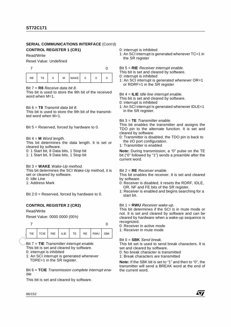
Obsolete Product(
s) - O
bsolete Product(
s)
ST72C171
86/152
SERIAL COMMUNICATIONS INTERFACE (Cont’d)
CONTROL REGISTER 1 (CR1)
Read/Write
Reset Value: Undefined
Bit 7 = R8 Receive data bit 8.This bit is used to store the 9th bit of the receivedword when M=1.
Bit 6 = T8 Transmit data bit 8.This bit is used to store the 9th bit of the transmit-ted word when M=1.
Bit 5 = Reserved, forced by hardware to 0.
Bit 4 = M Word length.This bit determines the data length. It is set orcleared by software.0: 1 Start bit, 8 Data bits, 1 Stop bit 1: 1 Start bit, 9 Data bits, 1 Stop bit
Bit 3 = WAKE Wake-Up method.This bit determines the SCI Wake-Up method, it isset or cleared by software.0: Idle Line1: Address Mark
Bit 2:0 = Reserved, forced by hardware to 0.
CONTROL REGISTER 2 (CR2)
Read/Write
Reset Value: 0000 0000 (00h)
Bit 7 = TIE Transmitter interrupt enable.This bit is set and cleared by software.0: interrupt is inhibited1: An SCI interrupt is generated whenever
TDRE=1 in the SR register.
Bit 6 = TCIE Transmission complete interrupt ena-ble
This bit is set and cleared by software.
0: interrupt is inhibited1: An SCI interrupt is generated whenever TC=1 in
the SR register
Bit 5 = RIE Receiver interrupt enable. This bit is set and cleared by software.0: interrupt is inhibited1: An SCI interrupt is generated whenever OR=1
or RDRF=1 in the SR register
Bit 4 = ILIE Idle line interrupt enable. This bit is set and cleared by software.0: interrupt is inhibited1: An SCI interrupt is generated whenever IDLE=1
in the SR register.
Bit 3 = TE Transmitter enable. This bit enables the transmitter and assigns theTDO pin to the alternate function. It is set andcleared by software. 0: Transmitter is disabled, the TDO pin is back to
the I/O port configuration.1: Transmitter is enabled
Note: During transmission, a “0” pulse on the TEbit (“0” followed by “1”) sends a preamble after thecurrent word.
Bit 2 = RE Receiver enable.This bit enables the receiver. It is set and clearedby software. 0: Receiver is disabled, it resets the RDRF, IDLE,
OR, NF and FE bits of the SR register.1: Receiver is enabled and begins searching for a
start bit.
Bit 1 = RWU Receiver wake-up.This bit determines if the SCI is in mute mode ornot. It is set and cleared by software and can becleared by hardware when a wake-up sequence isrecognized.0: Receiver in active mode1: Receiver in mute mode
Bit 0 = SBK Send break.This bit set is used to send break characters. It isset and cleared by software.0: No break character is transmitted1: Break characters are transmitted
Note: If the SBK bit is set to “1” and then to “0”, thetransmitter will send a BREAK word at the end ofthe current word.
7 0
R8 T8 0 M WAKE 0 0 0
7 0
TIE TCIE RIE ILIE TE RE RWU SBK
Obsolete Product(
s) - O
bsolete Product(
s)
ST72C171
87/152
SERIAL COMMUNICATIONS INTERFACE (Cont’d)
DATA REGISTER (DR)
Read/Write
Reset Value: Undefined
Contains the Received or Transmitted data char-acter, depending on whether it is read from or writ-ten to.
The Data register performs a double function (readand write) since it is composed of two registers,one for transmission (TDR) and one for reception(RDR).The TDR register provides the parallel interfacebetween the internal bus and the output shift reg-ister (see Figure 47).The RDR register provides the parallel interfacebetween the input shift register and the internalbus (see Figure 47).
BAUD RATE REGISTER (BRR)
Read/Write
Reset Value: 00xx xxxx (XXh)
Bit 7:6= SCP[1:0] First SCI Prescaler These 2 prescaling bits allow several standardclock division ranges:
Bit 5:3 = SCT[2:0] SCI Transmitter rate divisor
These 3 bits, in conjunction with the SCP1 & SCP0bits, define the total division applied to the busclock to yield the transmit rate clock in convention-al Baud Rate Generator mode.
Bit 2:0 = SCR[2:0] SCI Receiver rate divisor. These 3 bits, in conjunction with the SCP1 & SCP0bits, define the total division applied to the busclock to yield the receive rate clock in conventionalBaud Rate Generator mode.
7 0
DR7 DR6 DR5 DR4 DR3 DR2 DR1 DR0
7 0
SCP1 SCP0 SCT2 SCT1 SCT0 SCR2 SCR1 SCR0
PR Prescaling factor SCP1 SCP0
1 0 0
3 0 1
4 1 0
13 1 1
TR dividing factor SCT2 SCT1 SCT0
1 0 0 0
2 0 0 1
4 0 1 0
8 0 1 1
16 1 0 0
32 1 0 1
64 1 1 0
128 1 1 1
RR dividing factor SCR2 SCR1 SCR0
1 0 0 0
2 0 0 1
4 0 1 0
8 0 1 1
16 1 0 0
32 1 0 1
64 1 1 0
128 1 1 1
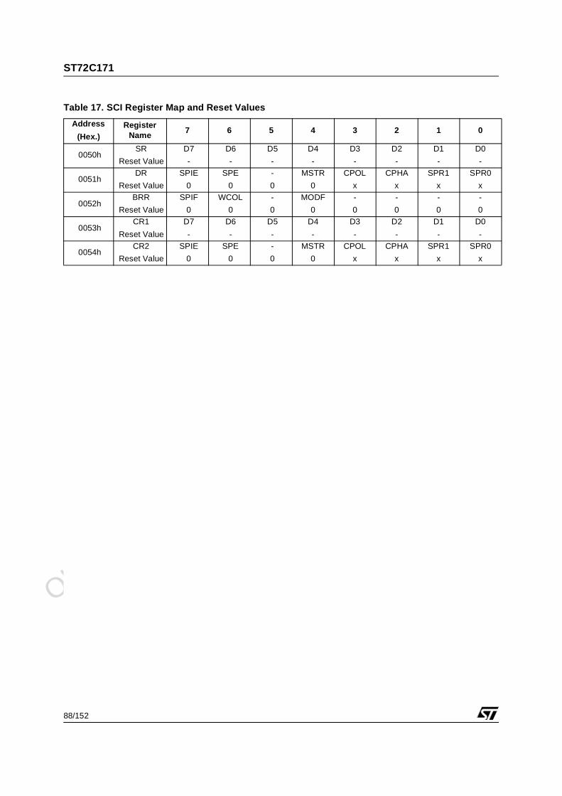
Obsolete Product(
s) - O
bsolete Product(
s)
ST72C171
88/152
Table 17. SCI Register Map and Reset Values
Address
(Hex.)Register
Name7 6 5 4 3 2 1 0
0050hSR
Reset Value
D7
-
D6
-
D5
-
D4
-
D3
-
D2
-
D1
-
D0
-
0051hDR
Reset Value
SPIE
0
SPE
0
-
0
MSTR
0
CPOL
x
CPHA
x
SPR1
x
SPR0
x
0052hBRR
Reset Value
SPIF
0
WCOL
0
-
0
MODF
0
-
0
-
0
-
0
-
0
0053hCR1
Reset Value
D7
-
D6
-
D5
-
D4
-
D3
-
D2
-
D1
-
D0
-
0054hCR2
Reset Value
SPIE
0
SPE
0
-
0
MSTR
0
CPOL
x
CPHA
x
SPR1
x
SPR0
x
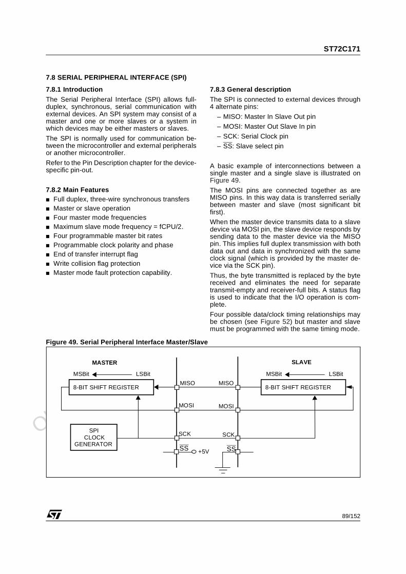
Obsolete Product(
s) - O
bsolete Product(
s)
ST72C171
89/152
7.8 SERIAL PERIPHERAL INTERFACE (SPI)
7.8.1 Introduction
The Serial Peripheral Interface (SPI) allows full-duplex, synchronous, serial communication withexternal devices. An SPI system may consist of amaster and one or more slaves or a system inwhich devices may be either masters or slaves.
The SPI is normally used for communication be-tween the microcontroller and external peripheralsor another microcontroller.
Refer to the Pin Description chapter for the device-specific pin-out.
7.8.2 Main Features Full duplex, three-wire synchronous transfers Master or slave operation Four master mode frequencies Maximum slave mode frequency = fCPU/2. Four programmable master bit rates Programmable clock polarity and phase End of transfer interrupt flag Write collision flag protection Master mode fault protection capability.
7.8.3 General description
The SPI is connected to external devices through4 alternate pins:
– MISO: Master In Slave Out pin
– MOSI: Master Out Slave In pin
– SCK: Serial Clock pin
– SS: Slave select pin
A basic example of interconnections between asingle master and a single slave is illustrated onFigure 49.
The MOSI pins are connected together as areMISO pins. In this way data is transferred seriallybetween master and slave (most significant bitfirst).
When the master device transmits data to a slavedevice via MOSI pin, the slave device responds bysending data to the master device via the MISOpin. This implies full duplex transmission with bothdata out and data in synchronized with the sameclock signal (which is provided by the master de-vice via the SCK pin).
Thus, the byte transmitted is replaced by the bytereceived and eliminates the need for separatetransmit-empty and receiver-full bits. A status flagis used to indicate that the I/O operation is com-plete.
Four possible data/clock timing relationships maybe chosen (see Figure 52) but master and slavemust be programmed with the same timing mode.
Figure 49. Serial Peripheral Interface Master/Slave
8-BIT SHIFT REGISTER
SPICLOCK
GENERATOR
8-BIT SHIFT REGISTERMISO
MOSI MOSI
MISO
SCK SCK
SLAVEMASTER
SS SS+5V
MSBit LSBit MSBit LSBit
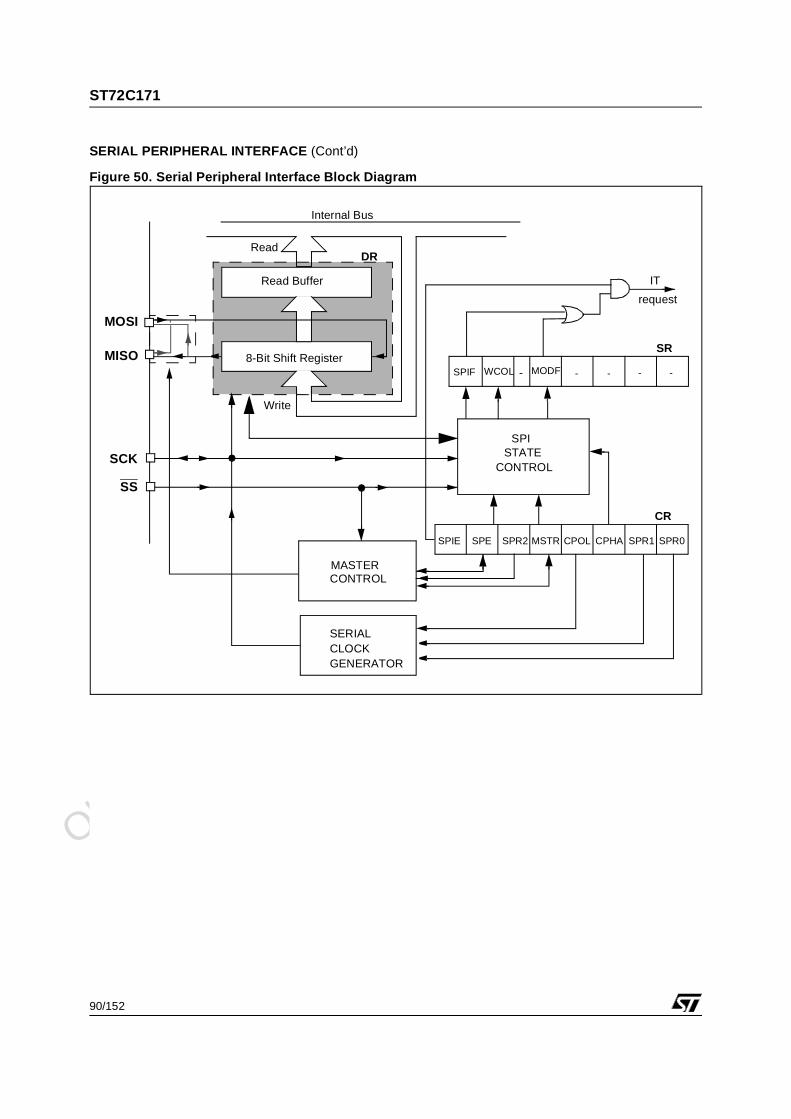
Obsolete Product(
s) - O
bsolete Product(
s)
ST72C171
90/152
SERIAL PERIPHERAL INTERFACE (Cont’d)
Figure 50. Serial Peripheral Interface Block Diagram
DR
Read Buffer
8-Bit Shift Register
Write
Read
Internal Bus
SPI
SPIE SPE SPR2 MSTR CPHA SPR0SPR1CPOL
SPIF WCOL MODF
SERIALCLOCKGENERATOR
MOSI
MISO
SS
SCK CONTROL
STATE
CR
SR
- - - - -
IT request
MASTERCONTROL
Obsolete Product(
s) - O
bsolete Product(
s)
ST72C171
91/152
SERIAL PERIPHERAL INTERFACE (Cont’d)
7.8.4 Functional Description
Figure 49 shows the serial peripheral interface(SPI) block diagram.
This interface contains 3 dedicated registers:
– A Control Register (CR)
– A Status Register (SR)
– A Data Register (DR)
Refer to the CR, SR and DR registers in Section9.8.7for the bit definitions.
7.8.4.1 Master ConfigurationIn a master configuration, the serial clock is gener-ated on the SCK pin.
Procedure
– Select the SPR0 & SPR1 bits to define the se-rial clock baud rate (see CR register).
– Select the CPOL and CPHA bits to define oneof the four relationships between the datatransfer and the serial clock (see Figure 52).
– The SS pin must be connected to a high levelsignal during the complete byte transmit se-quence.
– The MSTR and SPE bits must be set (they re-main set only if the SS pin is connected to ahigh level signal).
In this configuration the MOSI pin is a data outputand to the MISO pin is a data input.
Transmit sequence
The transmit sequence begins when a byte is writ-ten the DR register.
The data byte is parallel loaded into the 8-bit shiftregister (from the internal bus) during a write cycleand then shifted out serially to the MOSI pin mostsignificant bit first.
When data transfer is complete:
– The SPIF bit is set by hardware
– An interrupt is generated if the SPIE bit is setand the I bit in the CCR register is cleared.
During the last clock cycle the SPIF bit is set, acopy of the data byte received in the shift registeris moved to a buffer. When the DR register is read,the SPI peripheral returns this buffered value.
Clearing the SPIF bit is performed by the followingsoftware sequence:
1. An access to the SR register while the SPIF bitis set
2. A read to the DR register.
Note: While the SPIF bit is set, all writes to the DRregister are inhibited until the SR register is read.
Obsolete Product(
s) - O
bsolete Product(
s)
ST72C171
92/152
SERIAL PERIPHERAL INTERFACE (Cont’d)
7.8.4.2 Slave Configuration
In slave configuration, the serial clock is receivedon the SCK pin from the master device.
The value of the SPR0 & SPR1 bits is not used forthe data transfer.
Procedure– For correct data transfer, the slave device
must be in the same timing mode as the mas-ter device (CPOL and CPHA bits). See Figure52.
– The SS pin must be connected to a low levelsignal during the complete byte transmit se-quence.
– Clear the MSTR bit and set the SPE bit to as-sign the pins to alternate function.
In this configuration the MOSI pin is a data inputand the MISO pin is a data output.
Transmit Sequence
The data byte is parallel loaded into the 8-bit shiftregister (from the internal bus) during a write cycleand then shifted out serially to the MISO pin mostsignificant bit first.
The transmit sequence begins when the slave de-vice receives the clock signal and the most signifi-cant bit of the data on its MOSI pin.
When data transfer is complete:
– The SPIF bit is set by hardware
– An interrupt is generated if SPIE bit is set andI bit in CCR register is cleared.
During the last clock cycle the SPIF bit is set, acopy of the data byte received in the shift registeris moved to a buffer. When the DR register is read,the SPI peripheral returns this buffered value.
Clearing the SPIF bit is performed by the followingsoftware sequence:
1. An access to the SR register while the SPIF bitis set.
2.A read to the DR register.
Notes: While the SPIF bit is set, all writes to theDR register are inhibited until the SR register isread.
The SPIF bit can be cleared during a secondtransmission; however, it must be cleared beforethe second SPIF bit in order to prevent an overruncondition (see Section 9.8.4.6).
Depending on the CPHA bit, the SS pin has to beset to write to the DR register between each databyte transfer to avoid a write collision (see Section9.8.4.4).
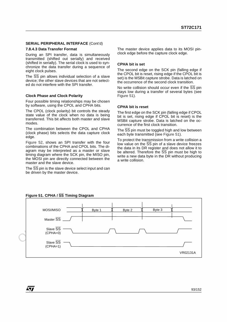
Obsolete Product(
s) - O
bsolete Product(
s)
ST72C171
93/152
SERIAL PERIPHERAL INTERFACE (Cont’d)
7.8.4.3 Data Transfer Format
During an SPI transfer, data is simultaneouslytransmitted (shifted out serially) and received(shifted in serially). The serial clock is used to syn-chronize the data transfer during a sequence ofeight clock pulses.
The SS pin allows individual selection of a slavedevice; the other slave devices that are not select-ed do not interfere with the SPI transfer.
Clock Phase and Clock Polarity
Four possible timing relationships may be chosenby software, using the CPOL and CPHA bits.
The CPOL (clock polarity) bit controls the steadystate value of the clock when no data is beingtransferred. This bit affects both master and slavemodes.
The combination between the CPOL and CPHA(clock phase) bits selects the data capture clockedge.
Figure 52, shows an SPI transfer with the fourcombinations of the CPHA and CPOL bits. The di-agram may be interpreted as a master or slavetiming diagram where the SCK pin, the MISO pin,the MOSI pin are directly connected between themaster and the slave device.
The SS pin is the slave device select input and canbe driven by the master device.
The master device applies data to its MOSI pin-clock edge before the capture clock edge.
CPHA bit is set
The second edge on the SCK pin (falling edge ifthe CPOL bit is reset, rising edge if the CPOL bit isset) is the MSBit capture strobe. Data is latched onthe occurrence of the second clock transition.
No write collision should occur even if the SS pinstays low during a transfer of several bytes (seeFigure 51).
CPHA bit is reset
The first edge on the SCK pin (falling edge if CPOLbit is set, rising edge if CPOL bit is reset) is theMSBit capture strobe. Data is latched on the oc-currence of the first clock transition.
The SS pin must be toggled high and low betweeneach byte transmitted (see Figure 51).
To protect the transmission from a write collision alow value on the SS pin of a slave device freezesthe data in its DR register and does not allow it tobe altered. Therefore the SS pin must be high towrite a new data byte in the DR without producinga write collision.
Figure 51. CPHA / SS Timing Diagram
MOSI/MISO
Master SS
Slave SS(CPHA=0)
Slave SS(CPHA=1)
Byte 1 Byte 2 Byte 3
VR02131A
Obsolete Product(
s) - O
bsolete Product(
s)
ST72C171
94/152
SERIAL PERIPHERAL INTERFACE (Cont’d)
Figure 52. Data Clock Timing Diagram
CPOL = 1)
CPOL = 0)
MISO(from master)
MOSI
(from slave)
SS
(to slave)
CAPTURE STROBE
CPHA =1
CPOL = 1
CPOL = 0
MSBit Bit 6 Bit 5 Bit 4 Bit3 Bit 2 Bit 1 LSBit
MSBit Bit 6 Bit 5 Bit 4 Bit3 Bit 2 Bit 1 LSBit
MISO(from master)
MOSI
SS(to slave)
CAPTURE STROBE
CPHA =0
Note: This figure should not be used as a replacement for parametric information.Refer to the Electrical Characteristics chapter.
(from slave)
VR02131B
MSBit Bit 6 Bit 5 Bit 4 Bit3 Bit 2 Bit 1 LSBit
MSBit Bit 6 Bit 5 Bit 4 Bit3 Bit 2 Bit 1 LSBit
SCLK (with
SCLK (with
Obsolete Product(
s) - O
bsolete Product(
s)
ST72C171
95/152
SERIAL PERIPHERAL INTERFACE (Cont’d)
7.8.4.4 Write Collision Error
A write collision occurs when the software tries towrite to the DR register while a data transfer is tak-ing place with an external device. When this hap-pens, the transfer continues uninterrupted; andthe software write will be unsuccessful.
Write collisions can occur both in master and slavemode.
Note: a "read collision" will never occur since thereceived data byte is placed in a buffer in whichaccess is always synchronous with the MCU oper-ation.
In Slave modeWhen the CPHA bit is set:
The slave device will receive a clock (SCK) edgeprior to the latch of the first data transfer. This firstclock edge will freeze the data in the slave deviceDR register and output the MSBit on to the exter-nal MISO pin of the slave device.
The SS pin low state enables the slave device butthe output of the MSBit onto the MISO pin doesnot take place until the first data transfer clockedge.
When the CPHA bit is reset:
Data is latched on the occurrence of the first clocktransition. The slave device does not have anyway of knowing when that transition will occur;therefore, the slave device collision occurs whensoftware attempts to write the DR register after itsSS pin has been pulled low.
For this reason, the SS pin must be high, betweeneach data byte transfer, to allow the CPU to writein the DR register without generating a write colli-sion.
In Master modeCollision in the master device is defined as a writeof the DR register while the internal serial clock(SCK) is in the process of transfer.
The SS pin signal must be always high on themaster device.
WCOL bit
The WCOL bit in the SR register is set if a writecollision occurs.
No SPI interrupt is generated when the WCOL bitis set (the WCOL bit is a status flag only).
Clearing the WCOL bit is done through a softwaresequence (see Figure 53).
Figure 53. Clearing the WCOL bit (Write Collision Flag) Software Sequence
Clearing sequence after SPIF = 1 (end of a data byte transfer)
1st Step Read SR
Read DR Write DR2nd Step SPIF =0WCOL=0
SPIF =0WCOL=0 if no transfer has startedWCOL=1 if a transfer has started
Clearing sequence before SPIF = 1 (during a data byte transfer)
1st Step
2nd Step WCOL=0
before the 2nd step
Read SR
Read DRNote: Writing in DR register in-stead of reading in it do not resetWCOL bit
Read SROR
THENTHEN
THEN
Obsolete Product(
s) - O
bsolete Product(
s)
ST72C171
96/152
SERIAL PERIPHERAL INTERFACE (Cont’d)
7.8.4.5 Master Mode Fault
Master mode fault occurs when the master devicehas its SS pin pulled low, then the MODF bit is set.
Master mode fault affects the SPI peripheral in thefollowing ways:
– The MODF bit is set and an SPI interrupt isgenerated if the SPIE bit is set.
– The SPE bit is reset. This blocks all outputfrom the device and disables the SPI periph-eral.
– The MSTR bit is reset, thus forcing the deviceinto slave mode.
Clearing the MODF bit is done through a softwaresequence:
1. A read or write access to the SR register whilethe MODF bit is set.
2. A write to the CR register.
Notes: To avoid any multiple slave conflicts in thecase of a system comprising several MCUs, theSS pin must be pulled high during the clearing se-quence of the MODF bit. The SPE and MSTR bits
may be restored to their original state during or af-ter this clearing sequence.
Hardware does not allow the user to set the SPEand MSTR bits while the MODF bit is set except inthe MODF bit clearing sequence.
In a slave device the MODF bit can not be set, butin a multi master configuration the device can be inslave mode with this MODF bit set.
The MODF bit indicates that there might havebeen a multi-master conflict for system control andallows a proper exit from system operation to a re-set or default system state using an interrupt rou-tine.
7.8.4.6 Overrun ConditionAn overrun condition occurs when the master de-vice has sent several data bytes and the slave de-vice has not cleared the SPIF bit issuing from theprevious data byte transmitted.
In this case, the receiver buffer contains the bytesent after the SPIF bit was last cleared. A read tothe DR register returns this byte. All other bytesare lost.
This condition is not detected by the SPI peripher-al.
Obsolete Product(
s) - O
bsolete Product(
s)
ST72C171
97/152
SERIAL PERIPHERAL INTERFACE (Cont’d)
7.8.4.7 Single Master and Multimaster Configurations
There are two types of SPI systems:
– Single Master System
– Multimaster System
Single Master SystemA typical single master system may be configured,using an MCU as the master and four MCUs asslaves (see Figure 54).
The master device selects the individual slave de-vices by using four pins of a parallel port to controlthe four SS pins of the slave devices.
The SS pins are pulled high during reset since themaster device ports will be forced to be inputs atthat time, thus disabling the slave devices.
Note: To prevent a bus conflict on the MISO linethe master allows only one active slave deviceduring a transmission.
For more security, the slave device may respondto the master with the received data byte. Then themaster will receive the previous byte back from theslave device if all MISO and MOSI pins are con-nected and the slave has not written its DR regis-ter.
Other transmission security methods can useports for handshake lines or data bytes with com-mand fields.
Multi-master System
A multi-master system may also be configured bythe user. Transfer of master control could be im-plemented using a handshake method through theI/O ports or by an exchange of code messagesthrough the serial peripheral interface system.
The multi-master system is principally handled bythe MSTR bit in the CR register and the MODF bitin the SR register.
Figure 54. Single Master Configuration
MISO
MOSI
MOSI
MOSI MOSI MOSIMISO MISO MISOMISO
SS
SS SS SS SSSCK SCKSCKSCK
SCK
5V
Por
ts
SlaveMCU
SlaveMCU
SlaveMCU
SlaveMCU
MasterMCU
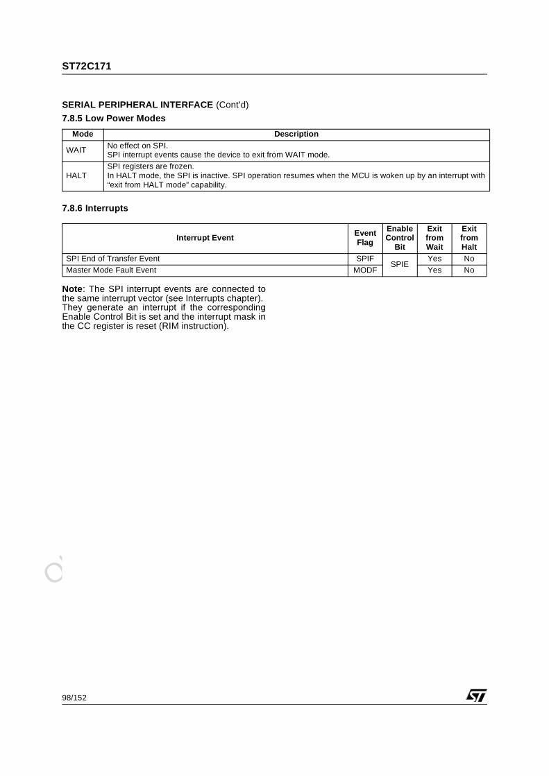
Obsolete Product(
s) - O
bsolete Product(
s)
ST72C171
98/152
SERIAL PERIPHERAL INTERFACE (Cont’d)
7.8.5 Low Power Modes
7.8.6 Interrupts
Note: The SPI interrupt events are connected tothe same interrupt vector (see Interrupts chapter). They generate an interrupt if the correspondingEnable Control Bit is set and the interrupt mask inthe CC register is reset (RIM instruction).
Mode Description
WAIT No effect on SPI. SPI interrupt events cause the device to exit from WAIT mode.
HALTSPI registers are frozen. In HALT mode, the SPI is inactive. SPI operation resumes when the MCU is woken up by an interrupt with “exit from HALT mode” capability.
Interrupt Event EventFlag
Enable Control
Bit
Exit fromWait
Exit from Halt
SPI End of Transfer Event SPIFSPIE
Yes No
Master Mode Fault Event MODF Yes No
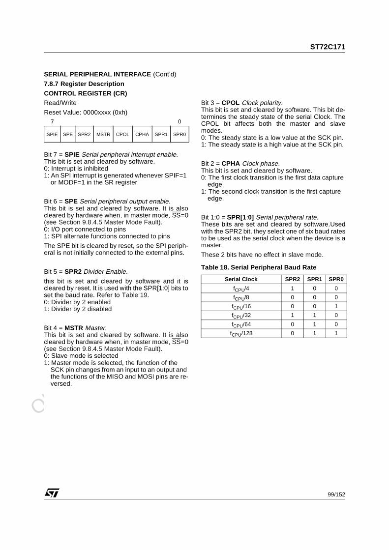
Obsolete Product(
s) - O
bsolete Product(
s)
ST72C171
99/152
SERIAL PERIPHERAL INTERFACE (Cont’d)
7.8.7 Register Description
CONTROL REGISTER (CR)Read/Write
Reset Value: 0000xxxx (0xh)
Bit 7 = SPIE Serial peripheral interrupt enable.This bit is set and cleared by software.0: Interrupt is inhibited1: An SPI interrupt is generated whenever SPIF=1
or MODF=1 in the SR register
Bit 6 = SPE Serial peripheral output enable.This bit is set and cleared by software. It is alsocleared by hardware when, in master mode, SS=0(see Section 9.8.4.5 Master Mode Fault).0: I/O port connected to pins1: SPI alternate functions connected to pins
The SPE bit is cleared by reset, so the SPI periph-eral is not initially connected to the external pins.
Bit 5 = SPR2 Divider Enable.
this bit is set and cleared by software and it iscleared by reset. It is used with the SPR[1:0] bits toset the baud rate. Refer to Table 19.0: Divider by 2 enabled1: Divider by 2 disabled
Bit 4 = MSTR Master.This bit is set and cleared by software. It is alsocleared by hardware when, in master mode, SS=0(see Section 9.8.4.5 Master Mode Fault).0: Slave mode is selected1: Master mode is selected, the function of the
SCK pin changes from an input to an output and the functions of the MISO and MOSI pins are re-versed.
Bit 3 = CPOL Clock polarity.This bit is set and cleared by software. This bit de-termines the steady state of the serial Clock. TheCPOL bit affects both the master and slavemodes. 0: The steady state is a low value at the SCK pin. 1: The steady state is a high value at the SCK pin.
Bit 2 = CPHA Clock phase.This bit is set and cleared by software.0: The first clock transition is the first data capture
edge.1: The second clock transition is the first capture
edge.
Bit 1:0 = SPR[1:0] Serial peripheral rate. These bits are set and cleared by software.Usedwith the SPR2 bit, they select one of six baud ratesto be used as the serial clock when the device is amaster.
These 2 bits have no effect in slave mode.
Table 18. Serial Peripheral Baud Rate
7 0
SPIE SPE SPR2 MSTR CPOL CPHA SPR1 SPR0
Serial Clock SPR2 SPR1 SPR0
fCPU/4 1 0 0
fCPU/8 0 0 0
fCPU/16 0 0 1
fCPU/32 1 1 0
fCPU/64 0 1 0
fCPU/128 0 1 1
Obsolete Product(
s) - O
bsolete Product(
s)
ST72C171
100/152
SERIAL PERIPHERAL INTERFACE (Cont’d)
STATUS REGISTER (SR)
Read Only
Reset Value: 0000 0000 (00h)
Bit 7 = SPIF Serial Peripheral data transfer flag.This bit is set by hardware when a transfer hasbeen completed. An interrupt is generated ifSPIE=1 in the CR register. It is cleared by a soft-ware sequence (an access to the SR register fol-lowed by a read or write to the DR register).0: Data transfer is in progress or has been ap-
proved by a clearing sequence.1: Data transfer between the device and an exter-
nal device has been completed.
Note: While the SPIF bit is set, all writes to the DRregister are inhibited.
Bit 6 = WCOL Write Collision status.
This bit is set by hardware when a write to the DRregister is done during a transmit sequence. It iscleared by a software sequence (see Figure 53).0: No write collision occurred1: A write collision has been detected
Bit 5 = Unused.
Bit 4 = MODF Mode Fault flag.This bit is set by hardware when the SS pin ispulled low in master mode (see Section 9.8.4.5Master Mode Fault). An SPI interrupt can be gen-erated if SPIE=1 in the CR register. This bit iscleared by a software sequence (An access to theSR register while MODF=1 followed by a write tothe CR register).0: No master mode fault detected1: A fault in master mode has been detected
Bits 3-0 = Unused.
DATA I/O REGISTER (DR)
Read/Write
Reset Value: Undefined
The DR register is used to transmit and receivedata on the serial bus. In the master device only awrite to this register will initiate transmission/re-ception of another byte.
Notes: During the last clock cycle the SPIF bit isset, a copy of the received data byte in the shiftregister is moved to a buffer. When the user readsthe serial peripheral data I/O register, the buffer isactually being read.
Warning:
A write to the DR register places data directly intothe shift register for transmission.
A write to the the DR register returns the value lo-cated in the buffer and not the contents of the shiftregister (See Figure 50 ).
7 0
SPIF WCOL - MODF - - - -
7 0
D7 D6 D5 D4 D3 D2 D1 D0

Obsolete Product(
s) - O
bsolete Product(
s)
ST72C171
101/152
Table 19. SPI Register Map and Reset Values
Address
(Hex.)Register
Name7 6 5 4 3 2 1 0
21DR
Reset Value
D7
-
D6
-
D5
-
D4
-
D3
-
D2
-
D1
-
D0
-
22CR
Reset Value
SPIE
0
SPE
0
-
0
MSTR
0
CPOL
x
CPHA
x
SPR1
x
SPR0
x
23SR
Reset Value
SPIF
0
WCOL
0
-
0
MODF
0
-
0
-
0
-
0
-
0
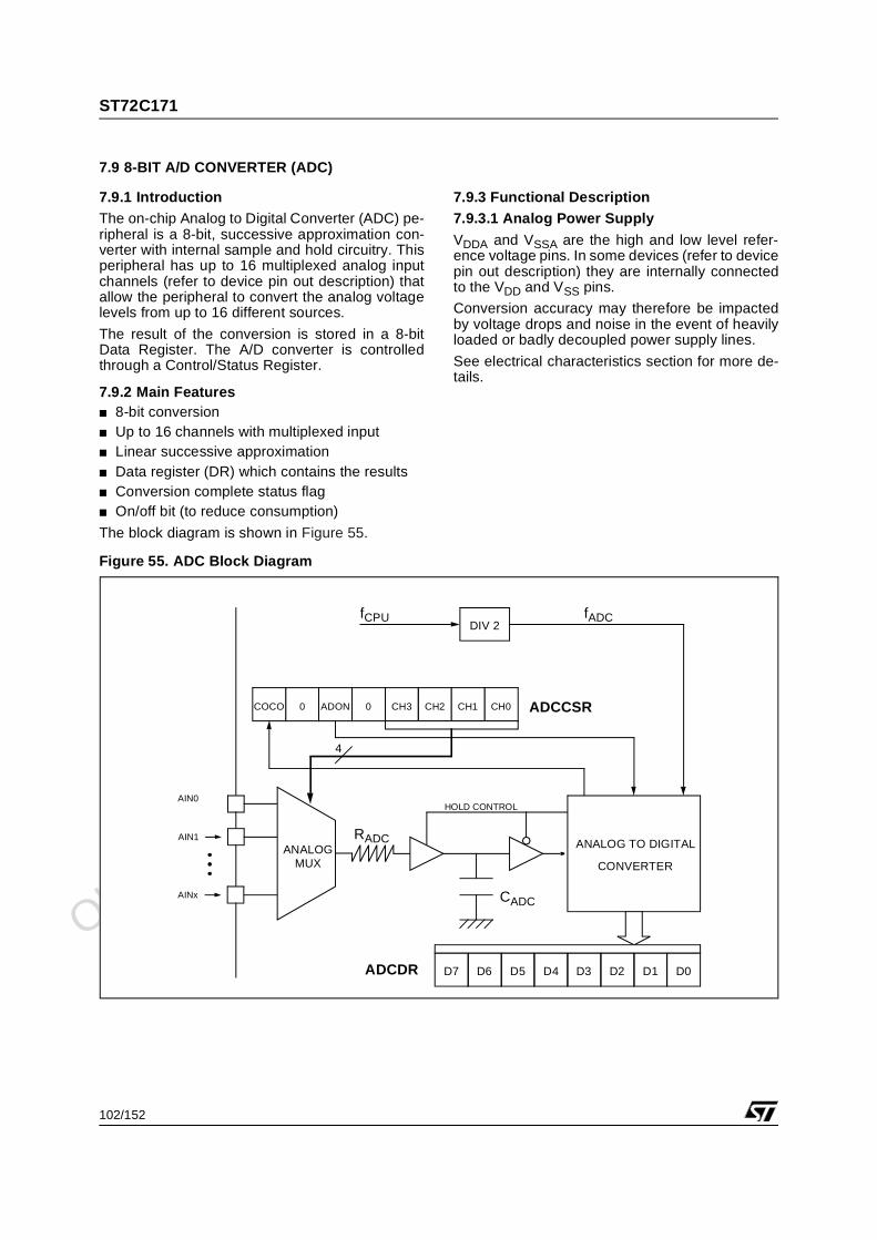
Obsolete Product(
s) - O
bsolete Product(
s)
ST72C171
102/152
7.9 8-BIT A/D CONVERTER (ADC)
7.9.1 IntroductionThe on-chip Analog to Digital Converter (ADC) pe-ripheral is a 8-bit, successive approximation con-verter with internal sample and hold circuitry. Thisperipheral has up to 16 multiplexed analog inputchannels (refer to device pin out description) thatallow the peripheral to convert the analog voltagelevels from up to 16 different sources.
The result of the conversion is stored in a 8-bitData Register. The A/D converter is controlledthrough a Control/Status Register.
7.9.2 Main Features 8-bit conversion Up to 16 channels with multiplexed input Linear successive approximation Data register (DR) which contains the results Conversion complete status flag On/off bit (to reduce consumption)
The block diagram is shown in Figure 55.
7.9.3 Functional Description7.9.3.1 Analog Power Supply
VDDA and VSSA are the high and low level refer-ence voltage pins. In some devices (refer to devicepin out description) they are internally connectedto the VDD and VSS pins.
Conversion accuracy may therefore be impactedby voltage drops and noise in the event of heavilyloaded or badly decoupled power supply lines.
See electrical characteristics section for more de-tails.
Figure 55. ADC Block Diagram
CH2 CH1CH3COCO 0 ADON 0 CH0 ADCCSR
AIN0
AIN1ANALOG TO DIGITAL
CONVERTER
AINx
ANALOGMUX
RADC
CADC
D2 D1D3D7 D6 D5 D4 D0ADCDR
4
DIV 2fADCfCPU
HOLD CONTROL
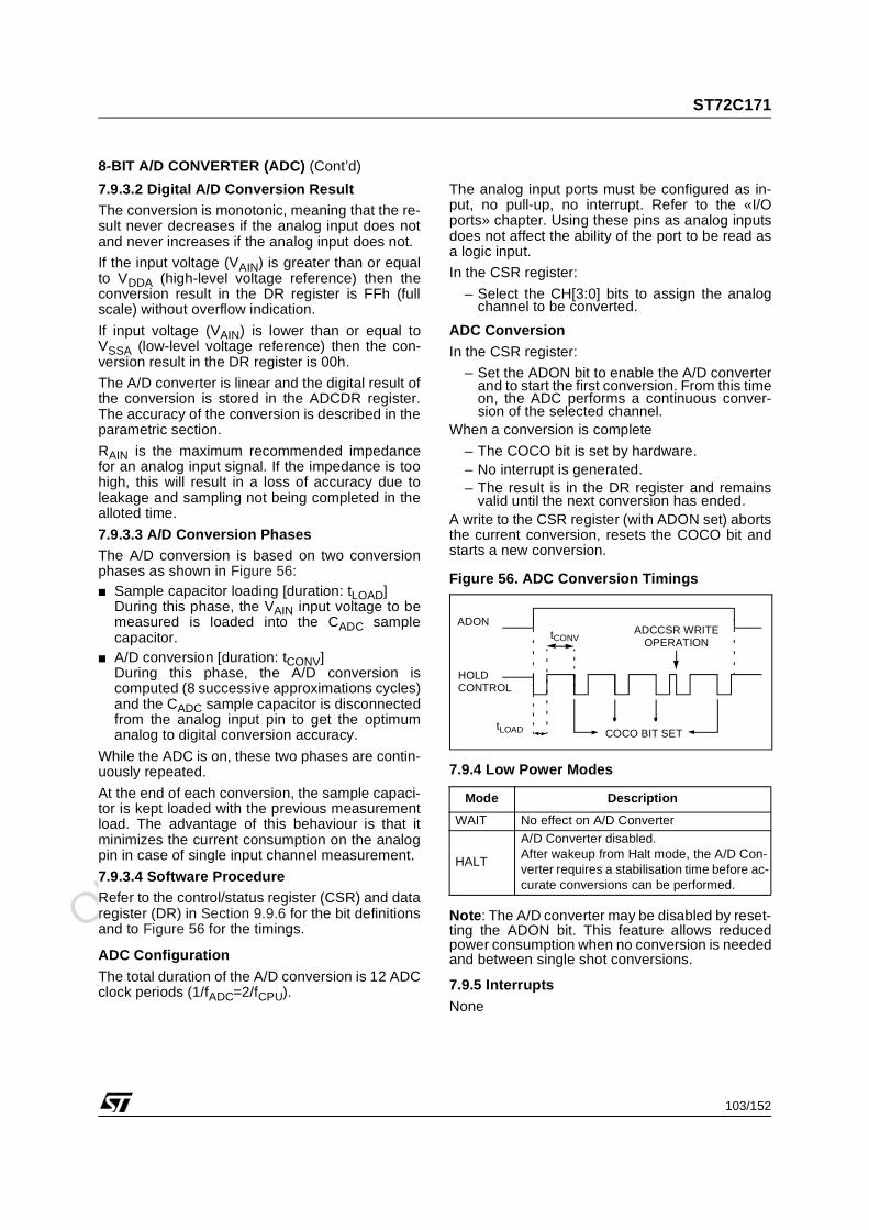
Obsolete Product(
s) - O
bsolete Product(
s)
ST72C171
103/152
8-BIT A/D CONVERTER (ADC) (Cont’d)
7.9.3.2 Digital A/D Conversion ResultThe conversion is monotonic, meaning that the re-sult never decreases if the analog input does notand never increases if the analog input does not.
If the input voltage (VAIN) is greater than or equalto VDDA (high-level voltage reference) then theconversion result in the DR register is FFh (fullscale) without overflow indication.
If input voltage (VAIN) is lower than or equal toVSSA (low-level voltage reference) then the con-version result in the DR register is 00h.
The A/D converter is linear and the digital result ofthe conversion is stored in the ADCDR register.The accuracy of the conversion is described in theparametric section.
RAIN is the maximum recommended impedancefor an analog input signal. If the impedance is toohigh, this will result in a loss of accuracy due toleakage and sampling not being completed in thealloted time.
7.9.3.3 A/D Conversion PhasesThe A/D conversion is based on two conversionphases as shown in Figure 56: Sample capacitor loading [duration: tLOAD]
During this phase, the VAIN input voltage to bemeasured is loaded into the CADC samplecapacitor.
A/D conversion [duration: tCONV]During this phase, the A/D conversion iscomputed (8 successive approximations cycles)and the CADC sample capacitor is disconnectedfrom the analog input pin to get the optimumanalog to digital conversion accuracy.
While the ADC is on, these two phases are contin-uously repeated.
At the end of each conversion, the sample capaci-tor is kept loaded with the previous measurementload. The advantage of this behaviour is that itminimizes the current consumption on the analogpin in case of single input channel measurement.
7.9.3.4 Software ProcedureRefer to the control/status register (CSR) and dataregister (DR) in Section 9.9.6 for the bit definitionsand to Figure 56 for the timings.
ADC Configuration
The total duration of the A/D conversion is 12 ADCclock periods (1/fADC=2/fCPU).
The analog input ports must be configured as in-put, no pull-up, no interrupt. Refer to the «I/Oports» chapter. Using these pins as analog inputsdoes not affect the ability of the port to be read asa logic input.
In the CSR register:
– Select the CH[3:0] bits to assign the analogchannel to be converted.
ADC Conversion
In the CSR register:
– Set the ADON bit to enable the A/D converterand to start the first conversion. From this timeon, the ADC performs a continuous conver-sion of the selected channel.
When a conversion is complete
– The COCO bit is set by hardware.– No interrupt is generated.– The result is in the DR register and remains
valid until the next conversion has ended.A write to the CSR register (with ADON set) abortsthe current conversion, resets the COCO bit andstarts a new conversion.
Figure 56. ADC Conversion Timings
7.9.4 Low Power Modes
Note: The A/D converter may be disabled by reset-ting the ADON bit. This feature allows reducedpower consumption when no conversion is neededand between single shot conversions.
7.9.5 Interrupts
None
Mode Description
WAIT No effect on A/D Converter
HALT
A/D Converter disabled. After wakeup from Halt mode, the A/D Con-verter requires a stabilisation time before ac-curate conversions can be performed.
ADCCSR WRITEADON
COCO BIT SETtLOAD
tCONV OPERATION
HOLDCONTROL
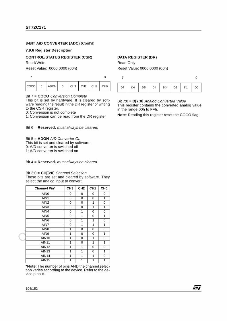
Obsolete Product(
s) - O
bsolete Product(
s)
ST72C171
104/152
8-BIT A/D CONVERTER (ADC) (Cont’d)
7.9.6 Register Description
CONTROL/STATUS REGISTER (CSR)Read/Write
Reset Value: 0000 0000 (00h)
Bit 7 = COCO Conversion CompleteThis bit is set by hardware. It is cleared by soft-ware reading the result in the DR register or writingto the CSR register.0: Conversion is not complete1: Conversion can be read from the DR register
Bit 6 = Reserved. must always be cleared.
Bit 5 = ADON A/D Converter OnThis bit is set and cleared by software.0: A/D converter is switched off1: A/D converter is switched on
Bit 4 = Reserved. must always be cleared.
Bit 3:0 = CH[3:0] Channel SelectionThese bits are set and cleared by software. Theyselect the analog input to convert.
*Note: The number of pins AND the channel selec-tion varies according to the device. Refer to the de-vice pinout.
DATA REGISTER (DR)Read Only
Reset Value: 0000 0000 (00h)
Bit 7:0 = D[7:0] Analog Converted ValueThis register contains the converted analog valuein the range 00h to FFh.
Note: Reading this register reset the COCO flag.
7 0
COCO 0 ADON 0 CH3 CH2 CH1 CH0
Channel Pin* CH3 CH2 CH1 CH0
AIN0 0 0 0 0AIN1 0 0 0 1AIN2 0 0 1 0AIN3 0 0 1 1AIN4 0 1 0 0AIN5 0 1 0 1AIN6 0 1 1 0AIN7 0 1 1 1AIN8 1 0 0 0AIN9 1 0 0 1AIN10 1 0 1 0AIN11 1 0 1 1AIN12 1 1 0 0AIN13 1 1 0 1AIN14 1 1 1 0AIN15 1 1 1 1
7 0
D7 D6 D5 D4 D3 D2 D1 D0
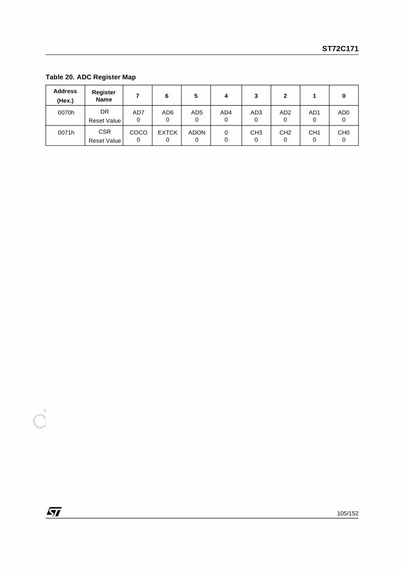
Obsolete Product(
s) - O
bsolete Product(
s)
ST72C171
105/152
Table 20. ADC Register Map
Address
(Hex.)Register
Name7 6 5 4 3 2 1 0
0070h DR
Reset ValueAD7
0AD6
0AD5
0AD4
0AD3
0AD2
0AD1
0AD0
0
0071h CSR
Reset ValueCOCO
0EXTCK
0ADON
000
CH30
CH20
CH10
CH00
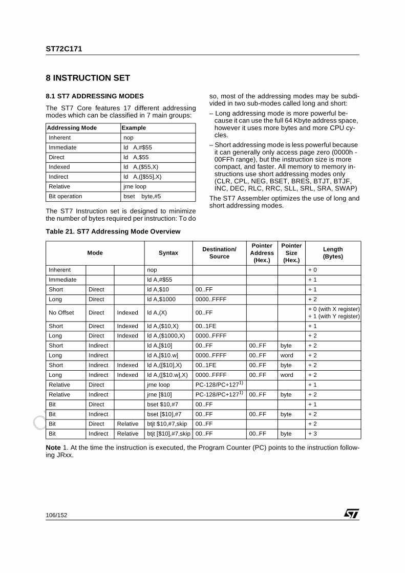
Obsolete Product(
s) - O
bsolete Product(
s)
ST72C171
106/152
8 INSTRUCTION SET
8.1 ST7 ADDRESSING MODES
The ST7 Core features 17 different addressingmodes which can be classified in 7 main groups:
The ST7 Instruction set is designed to minimizethe number of bytes required per instruction: To do
so, most of the addressing modes may be subdi-vided in two sub-modes called long and short:
– Long addressing mode is more powerful be-cause it can use the full 64 Kbyte address space, however it uses more bytes and more CPU cy-cles.
– Short addressing mode is less powerful because it can generally only access page zero (0000h - 00FFh range), but the instruction size is more compact, and faster. All memory to memory in-structions use short addressing modes only (CLR, CPL, NEG, BSET, BRES, BTJT, BTJF, INC, DEC, RLC, RRC, SLL, SRL, SRA, SWAP)
The ST7 Assembler optimizes the use of long andshort addressing modes.
Table 21. ST7 Addressing Mode Overview
Note 1. At the time the instruction is executed, the Program Counter (PC) points to the instruction follow-ing JRxx.
Addressing Mode Example
Inherent nop
Immediate ld A,#$55
Direct ld A,$55
Indexed ld A,($55,X)
Indirect ld A,([$55],X)
Relative jrne loop
Bit operation bset byte,#5
Mode SyntaxDestination/
Source
Pointer Address
(Hex.)
Pointer Size
(Hex.)
Length(Bytes)
Inherent nop + 0
Immediate ld A,#$55 + 1
Short Direct ld A,$10 00..FF + 1
Long Direct ld A,$1000 0000..FFFF + 2
No Offset Direct Indexed ld A,(X) 00..FF+ 0 (with X register)+ 1 (with Y register)
Short Direct Indexed ld A,($10,X) 00..1FE + 1
Long Direct Indexed ld A,($1000,X) 0000..FFFF + 2
Short Indirect ld A,[$10] 00..FF 00..FF byte + 2
Long Indirect ld A,[$10.w] 0000..FFFF 00..FF word + 2
Short Indirect Indexed ld A,([$10],X) 00..1FE 00..FF byte + 2
Long Indirect Indexed ld A,([$10.w],X) 0000..FFFF 00..FF word + 2
Relative Direct jrne loop PC-128/PC+1271) + 1
Relative Indirect jrne [$10] PC-128/PC+1271) 00..FF byte + 2
Bit Direct bset $10,#7 00..FF + 1
Bit Indirect bset [$10],#7 00..FF 00..FF byte + 2
Bit Direct Relative btjt $10,#7,skip 00..FF + 2
Bit Indirect Relative btjt [$10],#7,skip 00..FF 00..FF byte + 3
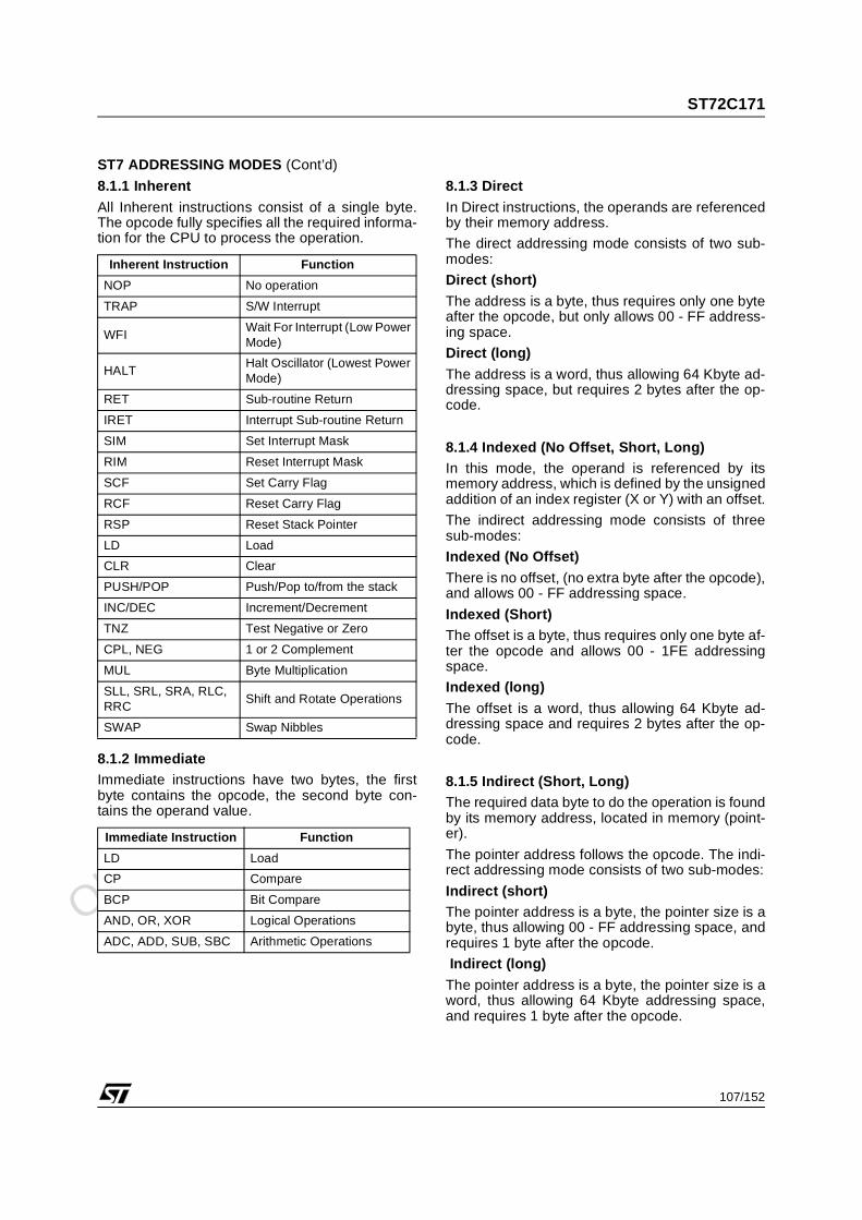
Obsolete Product(
s) - O
bsolete Product(
s)
ST72C171
107/152
ST7 ADDRESSING MODES (Cont’d)
8.1.1 Inherent
All Inherent instructions consist of a single byte.The opcode fully specifies all the required informa-tion for the CPU to process the operation.
8.1.2 ImmediateImmediate instructions have two bytes, the firstbyte contains the opcode, the second byte con-tains the operand value.
8.1.3 Direct
In Direct instructions, the operands are referencedby their memory address.
The direct addressing mode consists of two sub-modes:
Direct (short)
The address is a byte, thus requires only one byteafter the opcode, but only allows 00 - FF address-ing space.
Direct (long)
The address is a word, thus allowing 64 Kbyte ad-dressing space, but requires 2 bytes after the op-code.
8.1.4 Indexed (No Offset, Short, Long)In this mode, the operand is referenced by itsmemory address, which is defined by the unsignedaddition of an index register (X or Y) with an offset.
The indirect addressing mode consists of threesub-modes:
Indexed (No Offset)
There is no offset, (no extra byte after the opcode),and allows 00 - FF addressing space.
Indexed (Short)The offset is a byte, thus requires only one byte af-ter the opcode and allows 00 - 1FE addressingspace.
Indexed (long)
The offset is a word, thus allowing 64 Kbyte ad-dressing space and requires 2 bytes after the op-code.
8.1.5 Indirect (Short, Long)The required data byte to do the operation is foundby its memory address, located in memory (point-er).
The pointer address follows the opcode. The indi-rect addressing mode consists of two sub-modes:
Indirect (short)The pointer address is a byte, the pointer size is abyte, thus allowing 00 - FF addressing space, andrequires 1 byte after the opcode.
Indirect (long)
The pointer address is a byte, the pointer size is aword, thus allowing 64 Kbyte addressing space,and requires 1 byte after the opcode.
Inherent Instruction Function
NOP No operation
TRAP S/W Interrupt
WFIWait For Interrupt (Low Power Mode)
HALTHalt Oscillator (Lowest Power Mode)
RET Sub-routine Return
IRET Interrupt Sub-routine Return
SIM Set Interrupt Mask
RIM Reset Interrupt Mask
SCF Set Carry Flag
RCF Reset Carry Flag
RSP Reset Stack Pointer
LD Load
CLR Clear
PUSH/POP Push/Pop to/from the stack
INC/DEC Increment/Decrement
TNZ Test Negative or Zero
CPL, NEG 1 or 2 Complement
MUL Byte Multiplication
SLL, SRL, SRA, RLC, RRC
Shift and Rotate Operations
SWAP Swap Nibbles
Immediate Instruction Function
LD Load
CP Compare
BCP Bit Compare
AND, OR, XOR Logical Operations
ADC, ADD, SUB, SBC Arithmetic Operations
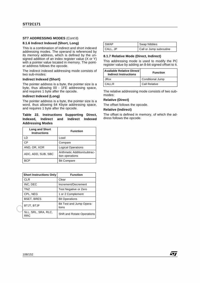
Obsolete Product(
s) - O
bsolete Product(
s)
ST72C171
108/152
ST7 ADDRESSING MODES (Cont’d)
8.1.6 Indirect Indexed (Short, Long)
This is a combination of indirect and short indexedaddressing modes. The operand is referenced byits memory address, which is defined by the un-signed addition of an index register value (X or Y)with a pointer value located in memory. The point-er address follows the opcode.
The indirect indexed addressing mode consists oftwo sub-modes:
Indirect Indexed (Short)The pointer address is a byte, the pointer size is abyte, thus allowing 00 - 1FE addressing space,and requires 1 byte after the opcode.
Indirect Indexed (Long)
The pointer address is a byte, the pointer size is aword, thus allowing 64 Kbyte addressing space,and requires 1 byte after the opcode.
Table 22. Instructions Supporting Direct,Indexed, Indirect and Indirect IndexedAddressing Modes
8.1.7 Relative Mode (Direct, Indirect)
This addressing mode is used to modify the PCregister value by adding an 8-bit signed offset to it.
The relative addressing mode consists of two sub-modes:
Relative (Direct)
The offset follows the opcode.
Relative (Indirect)
The offset is defined in memory, of which the ad-dress follows the opcode.
Long and Short Instructions
Function
LD Load
CP Compare
AND, OR, XOR Logical Operations
ADC, ADD, SUB, SBCArithmetic Addition/subtrac-tion operations
BCP Bit Compare
Short Instructions Only Function
CLR Clear
INC, DEC Increment/Decrement
TNZ Test Negative or Zero
CPL, NEG 1 or 2 Complement
BSET, BRES Bit Operations
BTJT, BTJFBit Test and Jump Opera-tions
SLL, SRL, SRA, RLC, RRC
Shift and Rotate Operations
SWAP Swap Nibbles
CALL, JP Call or Jump subroutine
Available Relative Direct/Indirect Instructions
Function
JRxx Conditional Jump
CALLR Call Relative
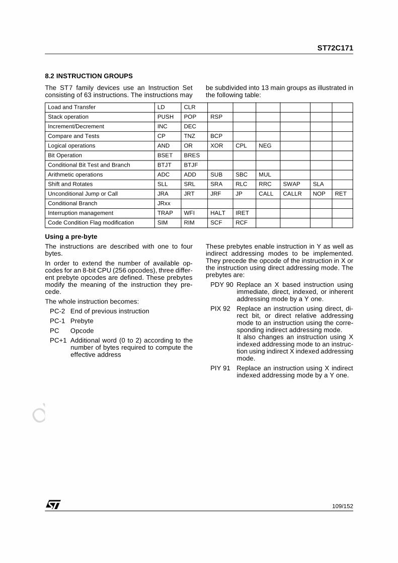
Obsolete Product(
s) - O
bsolete Product(
s)
ST72C171
109/152
8.2 INSTRUCTION GROUPS
The ST7 family devices use an Instruction Setconsisting of 63 instructions. The instructions may
be subdivided into 13 main groups as illustrated inthe following table:
Using a pre-byte
The instructions are described with one to fourbytes.
In order to extend the number of available op-codes for an 8-bit CPU (256 opcodes), three differ-ent prebyte opcodes are defined. These prebytesmodify the meaning of the instruction they pre-cede.
The whole instruction becomes:
PC-2 End of previous instruction
PC-1 Prebyte
PC Opcode
PC+1 Additional word (0 to 2) according to thenumber of bytes required to compute theeffective address
These prebytes enable instruction in Y as well asindirect addressing modes to be implemented.They precede the opcode of the instruction in X orthe instruction using direct addressing mode. Theprebytes are:
PDY 90 Replace an X based instruction usingimmediate, direct, indexed, or inherentaddressing mode by a Y one.
PIX 92 Replace an instruction using direct, di-rect bit, or direct relative addressingmode to an instruction using the corre-sponding indirect addressing mode.It also changes an instruction using Xindexed addressing mode to an instruc-tion using indirect X indexed addressingmode.
PIY 91 Replace an instruction using X indirectindexed addressing mode by a Y one.
Load and Transfer LD CLR
Stack operation PUSH POP RSP
Increment/Decrement INC DEC
Compare and Tests CP TNZ BCP
Logical operations AND OR XOR CPL NEG
Bit Operation BSET BRES
Conditional Bit Test and Branch BTJT BTJF
Arithmetic operations ADC ADD SUB SBC MUL
Shift and Rotates SLL SRL SRA RLC RRC SWAP SLA
Unconditional Jump or Call JRA JRT JRF JP CALL CALLR NOP RET
Conditional Branch JRxx
Interruption management TRAP WFI HALT IRET
Code Condition Flag modification SIM RIM SCF RCF
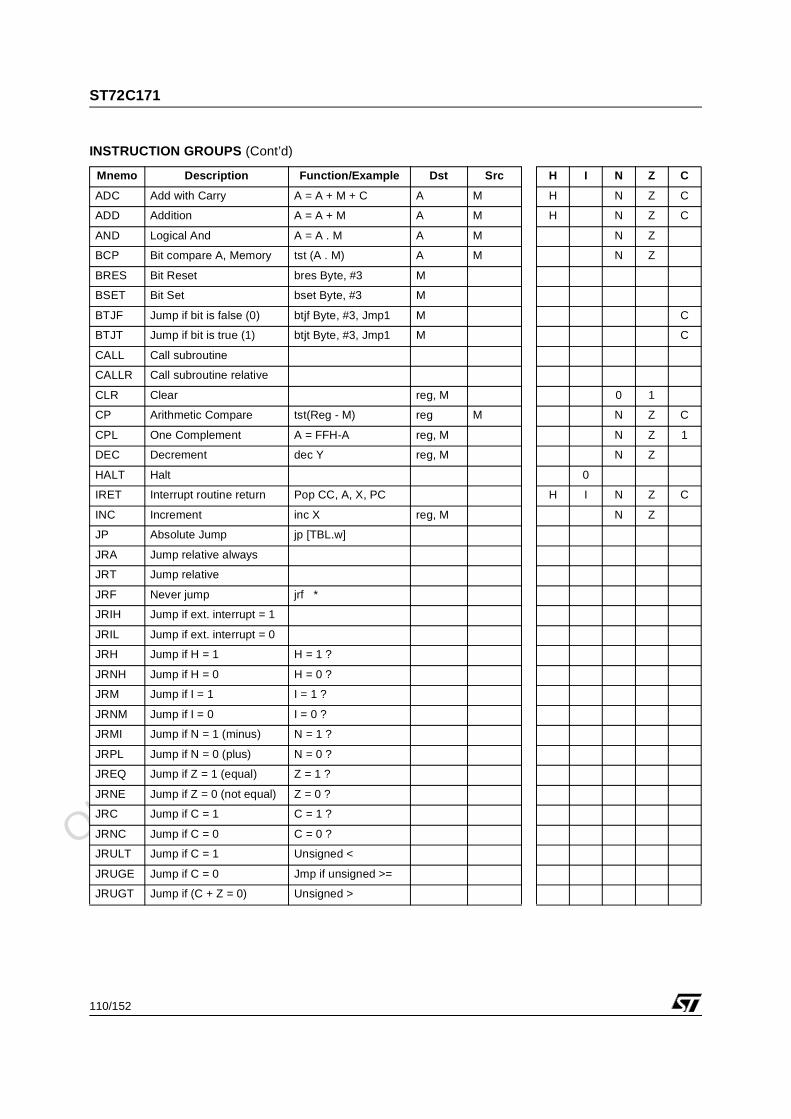
Obsolete Product(
s) - O
bsolete Product(
s)
ST72C171
110/152
INSTRUCTION GROUPS (Cont’d)
Mnemo Description Function/Example Dst Src H I N Z C
ADC Add with Carry A = A + M + C A M H N Z C
ADD Addition A = A + M A M H N Z C
AND Logical And A = A . M A M N Z
BCP Bit compare A, Memory tst (A . M) A M N Z
BRES Bit Reset bres Byte, #3 M
BSET Bit Set bset Byte, #3 M
BTJF Jump if bit is false (0) btjf Byte, #3, Jmp1 M C
BTJT Jump if bit is true (1) btjt Byte, #3, Jmp1 M C
CALL Call subroutine
CALLR Call subroutine relative
CLR Clear reg, M 0 1
CP Arithmetic Compare tst(Reg - M) reg M N Z C
CPL One Complement A = FFH-A reg, M N Z 1
DEC Decrement dec Y reg, M N Z
HALT Halt 0
IRET Interrupt routine return Pop CC, A, X, PC H I N Z C
INC Increment inc X reg, M N Z
JP Absolute Jump jp [TBL.w]
JRA Jump relative always
JRT Jump relative
JRF Never jump jrf *
JRIH Jump if ext. interrupt = 1
JRIL Jump if ext. interrupt = 0
JRH Jump if H = 1 H = 1 ?
JRNH Jump if H = 0 H = 0 ?
JRM Jump if I = 1 I = 1 ?
JRNM Jump if I = 0 I = 0 ?
JRMI Jump if N = 1 (minus) N = 1 ?
JRPL Jump if N = 0 (plus) N = 0 ?
JREQ Jump if Z = 1 (equal) Z = 1 ?
JRNE Jump if Z = 0 (not equal) Z = 0 ?
JRC Jump if C = 1 C = 1 ?
JRNC Jump if C = 0 C = 0 ?
JRULT Jump if C = 1 Unsigned <
JRUGE Jump if C = 0 Jmp if unsigned >=
JRUGT Jump if (C + Z = 0) Unsigned >
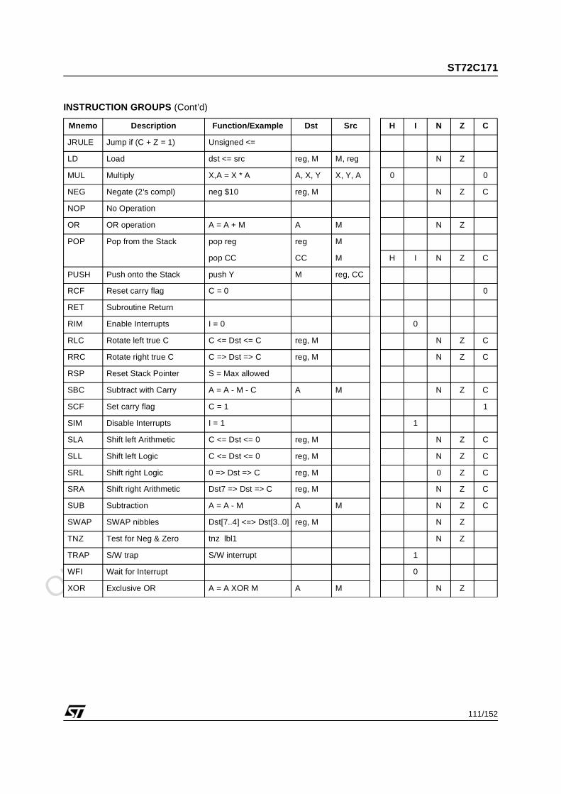
Obsolete Product(
s) - O
bsolete Product(
s)
ST72C171
111/152
INSTRUCTION GROUPS (Cont’d)
Mnemo Description Function/Example Dst Src H I N Z C
JRULE Jump if (C + Z = 1) Unsigned <=
LD Load dst <= src reg, M M, reg N Z
MUL Multiply X,A = X * A A, X, Y X, Y, A 0 0
NEG Negate (2’s compl) neg $10 reg, M N Z C
NOP No Operation
OR OR operation A = A + M A M N Z
POP Pop from the Stack pop reg reg M
pop CC CC M H I N Z C
PUSH Push onto the Stack push Y M reg, CC
RCF Reset carry flag C = 0 0
RET Subroutine Return
RIM Enable Interrupts I = 0 0
RLC Rotate left true C C <= Dst <= C reg, M N Z C
RRC Rotate right true C C => Dst => C reg, M N Z C
RSP Reset Stack Pointer S = Max allowed
SBC Subtract with Carry A = A - M - C A M N Z C
SCF Set carry flag C = 1 1
SIM Disable Interrupts I = 1 1
SLA Shift left Arithmetic C <= Dst <= 0 reg, M N Z C
SLL Shift left Logic C <= Dst <= 0 reg, M N Z C
SRL Shift right Logic 0 => Dst => C reg, M 0 Z C
SRA Shift right Arithmetic Dst7 => Dst => C reg, M N Z C
SUB Subtraction A = A - M A M N Z C
SWAP SWAP nibbles Dst[7..4] <=> Dst[3..0] reg, M N Z
TNZ Test for Neg & Zero tnz lbl1 N Z
TRAP S/W trap S/W interrupt 1
WFI Wait for Interrupt 0
XOR Exclusive OR A = A XOR M A M N Z
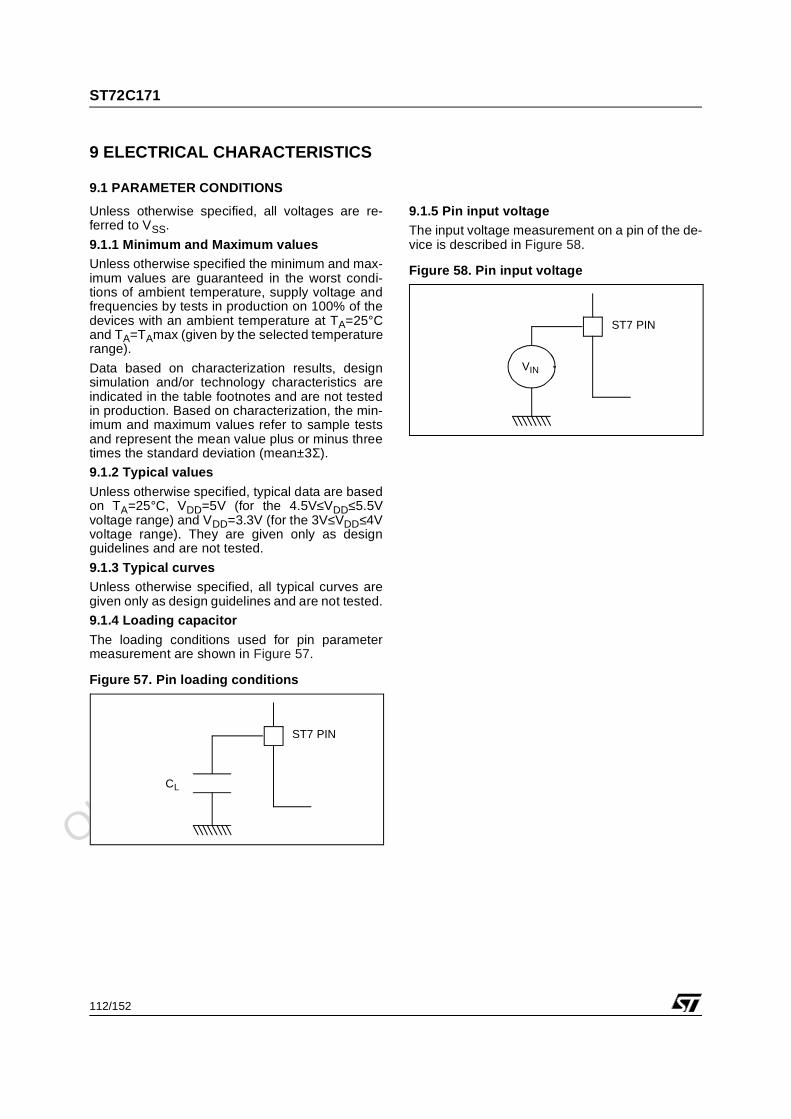
Obsolete Product(
s) - O
bsolete Product(
s)
ST72C171
112/152
9 ELECTRICAL CHARACTERISTICS
9.1 PARAMETER CONDITIONS
Unless otherwise specified, all voltages are re-ferred to VSS.
9.1.1 Minimum and Maximum valuesUnless otherwise specified the minimum and max-imum values are guaranteed in the worst condi-tions of ambient temperature, supply voltage andfrequencies by tests in production on 100% of thedevices with an ambient temperature at TA=25°Cand TA=TAmax (given by the selected temperaturerange).
Data based on characterization results, designsimulation and/or technology characteristics areindicated in the table footnotes and are not testedin production. Based on characterization, the min-imum and maximum values refer to sample testsand represent the mean value plus or minus threetimes the standard deviation (mean±3Σ).
9.1.2 Typical values
Unless otherwise specified, typical data are basedon TA=25°C, VDD=5V (for the 4.5V≤VDD≤5.5Vvoltage range) and VDD=3.3V (for the 3V≤VDD≤4Vvoltage range). They are given only as designguidelines and are not tested.
9.1.3 Typical curvesUnless otherwise specified, all typical curves aregiven only as design guidelines and are not tested.
9.1.4 Loading capacitor
The loading conditions used for pin parametermeasurement are shown in Figure 57.
Figure 57. Pin loading conditions
9.1.5 Pin input voltageThe input voltage measurement on a pin of the de-vice is described in Figure 58.
Figure 58. Pin input voltage
CL
ST7 PIN
VIN
ST7 PIN
Obsolete Product(
s) - O
bsolete Product(
s)
ST72C171
113/152
9.2 ABSOLUTE MAXIMUM RATINGS
Stresses above those listed as “absolute maxi-mum ratings” may cause permanent damage tothe device. This is a stress rating only and func-tional operation of the device under these condi-
tions is not implied. Exposure to maximum ratingconditions for extended periods may affect devicereliability.
9.2.1 Voltage Characteristics
9.2.2 Current Characteristics
9.2.3 Thermal Characteristics
Notes:1. Directly connecting the RESET and I/O pins to VDD or VSS could damage the device if an unintentional internal resetis generated or an unexpected change of the I/O configuration occurs (for example, due to a corrupted program counter).To guarantee safe operation, this connection has to be done through a pull-up or pull-down resistor (typical: 4.7kΩ forRESET, 10kΩ for I/Os). Unused I/O pins must be tied in the same way to VDD or VSS according to their reset configuration.2. When the current limitation is not possible, the VIN absolute maximum rating must be respected, otherwise refer toIINJ(PIN) specification. A positive injection is induced by VIN>VDD while a negative injection is induced by VIN<VSS.3. All power (VDD) and ground (VSS) lines must always be connected to the external supply.4. Negative injection disturbs the analog performance of the device. In particular, it induces leakage currents throughoutthe device including the analog inputs. To avoid undesirable effects on the analog functions, care must be taken:- Analog input pins must have a negative injection less than 0.8 mA (assuming that the impedance of the analog voltageis lower than the specified limits)- Pure digital pins must have a negative injection less than 1.6mA. In addition, it is recommended to inject the current asfar as possible from the analog input pins.5. When several inputs are submitted to a current injection, the maximum ΣIINJ(PIN) is the absolute sum of the positiveand negative injected currents (instantaneous values). These results are based on characterisation with ΣIINJ(PIN) maxi-mum current injection on four I/O port pins of the device.6. True open drain I/O port pins do not accept positive injection.
Symbol Ratings Maximum value Unit
VDD - VSS Supply voltage 6.5V
VIN Input voltage on any pin 1) & 2) VSS-0.3 to VDD+0.3
VESD(HBM) Electro-static discharge voltage (Human Body Model) see Section 9.7.2 Absolute Electri-cal SensitivityVESD(MM) Electro-static discharge voltage (Machine Model)
Symbol Ratings Maximum value Unit
IVDD Total current into VDD power lines (source) 3) 80
mA
IVSS Total current out of VSS ground lines (sink) 3) 80
IIO
Output current sunk by any standard I/O and control pin 25
Output current sunk by any high sink I/O pin 50
Output current source by any I/Os and control pin - 25
IINJ(PIN) 2) & 4)
Injected current on ISPSEL pin ± 5
Injected current on RESET pin ± 5
Injected current on OSC1 and OSC2 pins ± 5
Injected current on any other pin 5) & 6) ± 5
ΣIINJ(PIN) 2) Total injected current (sum of all I/O and control pins) 5) ± 20
Symbol Ratings Value Unit
TSTG Storage temperature range -65 to +150 °C
TJMaximum junction temperature(see Section 10.2 THERMAL CHARACTERISTICS )
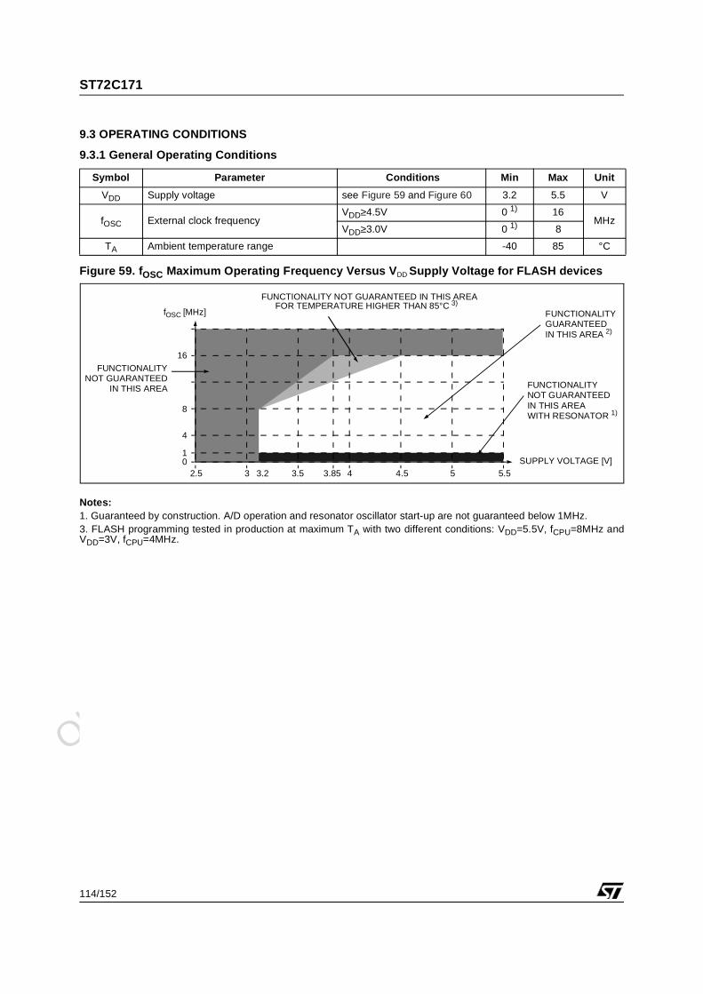
Obsolete Product(
s) - O
bsolete Product(
s)
ST72C171
114/152
9.3 OPERATING CONDITIONS
9.3.1 General Operating Conditions
Figure 59. fOSC Maximum Operating Frequency Versus VDD Supply Voltage for FLASH devices
Notes:1. Guaranteed by construction. A/D operation and resonator oscillator start-up are not guaranteed below 1MHz.3. FLASH programming tested in production at maximum TA with two different conditions: VDD=5.5V, fCPU=8MHz andVDD=3V, fCPU=4MHz.
Symbol Parameter Conditions Min Max Unit
VDD Supply voltage see Figure 59 and Figure 60 3.2 5.5 V
fOSC External clock frequencyVDD≥4.5V 0 1) 16
MHzVDD≥3.0V 0 1) 8
TA Ambient temperature range -40 85 °C
fOSC [MHz]
SUPPLY VOLTAGE [V]
16
8
4
10
2.5 3 3.5 4 4.5 5 5.5
FUNCTIONALITY
FUNCTIONALITY
FUNCTIONALITYGUARANTEEDIN THIS AREA 2)
NOT GUARANTEEDIN THIS AREA
NOT GUARANTEEDIN THIS AREAWITH RESONATOR 1)
FUNCTIONALITY NOT GUARANTEED IN THIS AREAFOR TEMPERATURE HIGHER THAN 85°C 3)
3.853.2
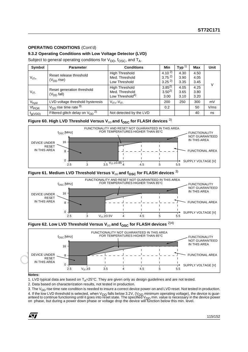
Obsolete Product(
s) - O
bsolete Product(
s)
ST72C171
115/152
OPERATING CONDITIONS (Cont’d)
9.3.2 Operating Conditions with Low Voltage Detector (LVD)
Subject to general operating conditions for VDD, fOSC, and TA.
Figure 60. High LVD Threshold Versus VDD and fOSC for FLASH devices 3)
Figure 61. Medium LVD Threshold Versus VDD and fOSC for FLASH devices 3)
Figure 62. Low LVD Threshold Versus VDD and fOSC for FLASH devices 2)4)
Notes:1. LVD typical data are based on TA=25°C. They are given only as design guidelines and are not tested.2. Data based on characterization results, not tested in production.3. The VDD rise time rate condition is needed to insure a correct device power-on and LVD reset. Not tested in production.4. If the low LVD threshold is selected, when VDD falls below 3.2V, (VDD minimum operating voltage), the device is guar-anteed to continue functioning until it goes into reset state. The specified VDD min. value is necessary in the device poweron phase, but during a power down phase or voltage drop the device will function below this min. level.
Symbol Parameter Conditions Min Typ 1) Max Unit
VIT+Reset release threshold(VDD rise)
High ThresholdMed. ThresholdLow Threshold
4.10 2)
3.75 2)
3.25 2)
4.303.903.35
4.504.053.45
V
VIT-Reset generation threshold(VDD fall)
High ThresholdMed. ThresholdLow Threshold4)
3.852)
3.502)
3.00
4.053.653.10
4.253.803.20
Vhyst LVD voltage threshold hysteresis VIT+-VIT- 200 250 300 mV
VtPOR VDD rise time rate 3) 0.2 50 V/ms
tg(VDD) Filtered glitch delay on VDD 2) Not detected by the LVD 40 ns
fOSC [MHz]
SUPPLY VOLTAGE [V]
16
8
02.5 3 3.5 4 4.5 5 5.5
FUNCTIONAL AREA
DEVICE UNDER
FUNCTIONALITY AND RESET NOT GUARANTEED IN THIS AREAFOR TEMPERATURES HIGHER THAN 85°C
RESETIN THIS AREA
FUNCTIONALITYNOT GUARANTEEDIN THIS AREA
VIT-≥3.85
fOSC [MHz]
SUPPLY VOLTAGE [V]
16
8
02.5 3 VIT-≥3.5V 4 4.5 5 5.5
FUNCTIONAL AREA
DEVICE UNDER
FUNCTIONALITY AND RESET NOT GUARANTEED IN THIS AREAFOR TEMPERATURES HIGHER THAN 85°C
RESETIN THIS AREA
FUNCTIONALITYNOT GUARANTEEDIN THIS AREA
fOSC [MHz]
SUPPLY VOLTAGE [V]
16
8
02.5 VIT-≥3 3.5 4 4.5 5 5.5
FUNCTIONAL AREADEVICE UNDER
FUNCTIONALITY NOT GUARANTEED IN THIS AREAFOR TEMPERATURES HIGHER THAN 85°C
RESETIN THIS AREA
FUNCTIONALITYNOT GUARANTEEDIN THIS AREA
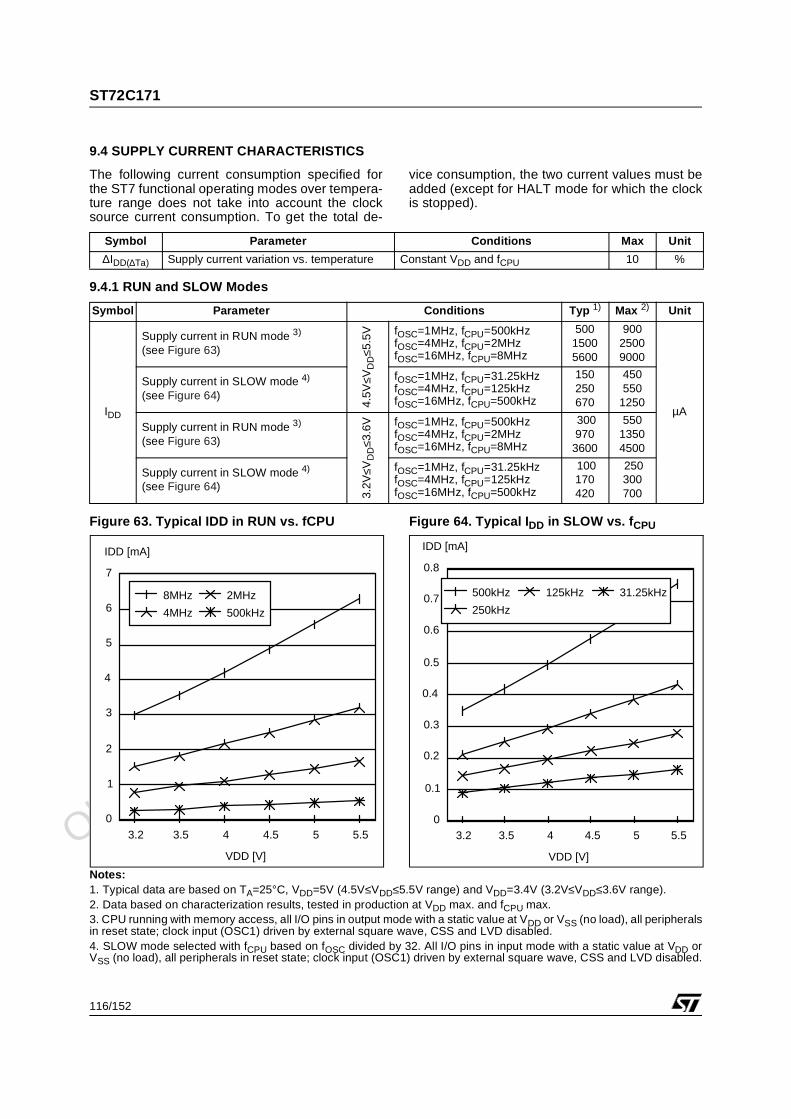
Obsolete Product(
s) - O
bsolete Product(
s)
ST72C171
116/152
9.4 SUPPLY CURRENT CHARACTERISTICS
The following current consumption specified forthe ST7 functional operating modes over tempera-ture range does not take into account the clocksource current consumption. To get the total de-
vice consumption, the two current values must beadded (except for HALT mode for which the clockis stopped).
9.4.1 RUN and SLOW Modes
Figure 63. Typical IDD in RUN vs. fCPU Figure 64. Typical IDD in SLOW vs. fCPU
Notes:1. Typical data are based on TA=25°C, VDD=5V (4.5V≤VDD≤5.5V range) and VDD=3.4V (3.2V≤VDD≤3.6V range).2. Data based on characterization results, tested in production at VDD max. and fCPU max.3. CPU running with memory access, all I/O pins in output mode with a static value at VDD or VSS (no load), all peripheralsin reset state; clock input (OSC1) driven by external square wave, CSS and LVD disabled.4. SLOW mode selected with fCPU based on fOSC divided by 32. All I/O pins in input mode with a static value at VDD orVSS (no load), all peripherals in reset state; clock input (OSC1) driven by external square wave, CSS and LVD disabled.
Symbol Parameter Conditions Max Unit
∆IDD(∆Ta) Supply current variation vs. temperature Constant VDD and fCPU 10 %
Symbol Parameter Conditions Typ 1) Max 2) Unit
IDD
Supply current in RUN mode 3)
(see Figure 63)4.
5V≤V
DD
≤5.5
V fOSC=1MHz, fCPU=500kHzfOSC=4MHz, fCPU=2MHzfOSC=16MHz, fCPU=8MHz
50015005600
90025009000
µA
Supply current in SLOW mode 4)
(see Figure 64)
fOSC=1MHz, fCPU=31.25kHzfOSC=4MHz, fCPU=125kHzfOSC=16MHz, fCPU=500kHz
150250670
450550
1250
Supply current in RUN mode 3)
(see Figure 63)
3.2V
≤VD
D≤3
.6V fOSC=1MHz, fCPU=500kHz
fOSC=4MHz, fCPU=2MHzfOSC=16MHz, fCPU=8MHz
300970
3600
55013504500
Supply current in SLOW mode 4)
(see Figure 64)
fOSC=1MHz, fCPU=31.25kHzfOSC=4MHz, fCPU=125kHzfOSC=16MHz, fCPU=500kHz
100170420
250300700
3.2 3.5 4 4.5 5 5.5
VDD [V]
0
1
2
3
4
5
6
7
IDD [mA]
8MHz
4MHz
2MHz
500kHz
3.2 3.5 4 4.5 5 5.5
VDD [V]
0
0.1
0.2
0.3
0.4
0.5
0.6
0.7
0.8
IDD [mA]
500kHz
250kHz
125kHz 31.25kHz
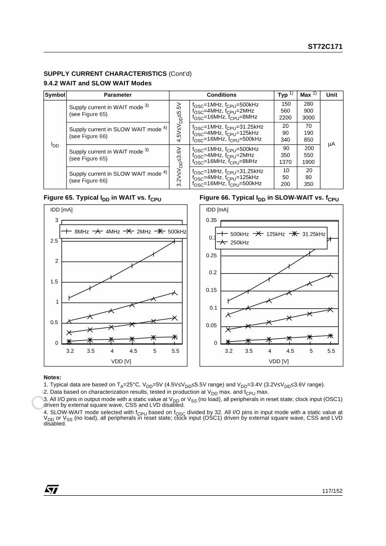
Obsolete Product(
s) - O
bsolete Product(
s)
ST72C171
117/152
SUPPLY CURRENT CHARACTERISTICS (Cont’d)
9.4.2 WAIT and SLOW WAIT Modes
Figure 65. Typical IDD in WAIT vs. fCPU Figure 66. Typical IDD in SLOW-WAIT vs. fCPU
Notes:1. Typical data are based on TA=25°C, VDD=5V (4.5V≤VDD≤5.5V range) and VDD=3.4V (3.2V≤VDD≤3.6V range).2. Data based on characterization results, tested in production at VDD max. and fCPU max.3. All I/O pins in output mode with a static value at VDD or VSS (no load), all peripherals in reset state; clock input (OSC1)driven by external square wave, CSS and LVD disabled.4. SLOW-WAIT mode selected with fCPU based on fOSC divided by 32. All I/O pins in input mode with a static value atVDD or VSS (no load), all peripherals in reset state; clock input (OSC1) driven by external square wave, CSS and LVDdisabled.
Symbol Parameter Conditions Typ 1) Max 2) Unit
IDD
Supply current in WAIT mode 3)
(see Figure 65)
4.5V
≤VD
D≤5
.5V fOSC=1MHz, fCPU=500kHz
fOSC=4MHz, fCPU=2MHzfOSC=16MHz, fCPU=8MHz
150560
2200
280900
3000
µA
Supply current in SLOW WAIT mode 4)
(see Figure 66)
fOSC=1MHz, fCPU=31.25kHzfOSC=4MHz, fCPU=125kHzfOSC=16MHz, fCPU=500kHz
2090
340
70190850
Supply current in WAIT mode 3)
(see Figure 65)
3.2V
≤VD
D≤3
.6V fOSC=1MHz, fCPU=500kHz
fOSC=4MHz, fCPU=2MHzfOSC=16MHz, fCPU=8MHz
90350
1370
200550
1900
Supply current in SLOW WAIT mode 4)
(see Figure 66)
fOSC=1MHz, fCPU=31.25kHzfOSC=4MHz, fCPU=125kHzfOSC=16MHz, fCPU=500kHz
1050
200
2080
350
3.2 3.5 4 4.5 5 5.5
VDD [V]
0
0.5
1
1.5
2
2.5
3
IDD [mA]
8MHz 4MHz 2MHz 500kHz
3.2 3.5 4 4.5 5 5.5
VDD [V]
0
0.05
0.1
0.15
0.2
0.25
0.3
0.35
IDD [mA]
500kHz
250kHz
125kHz 31.25kHz
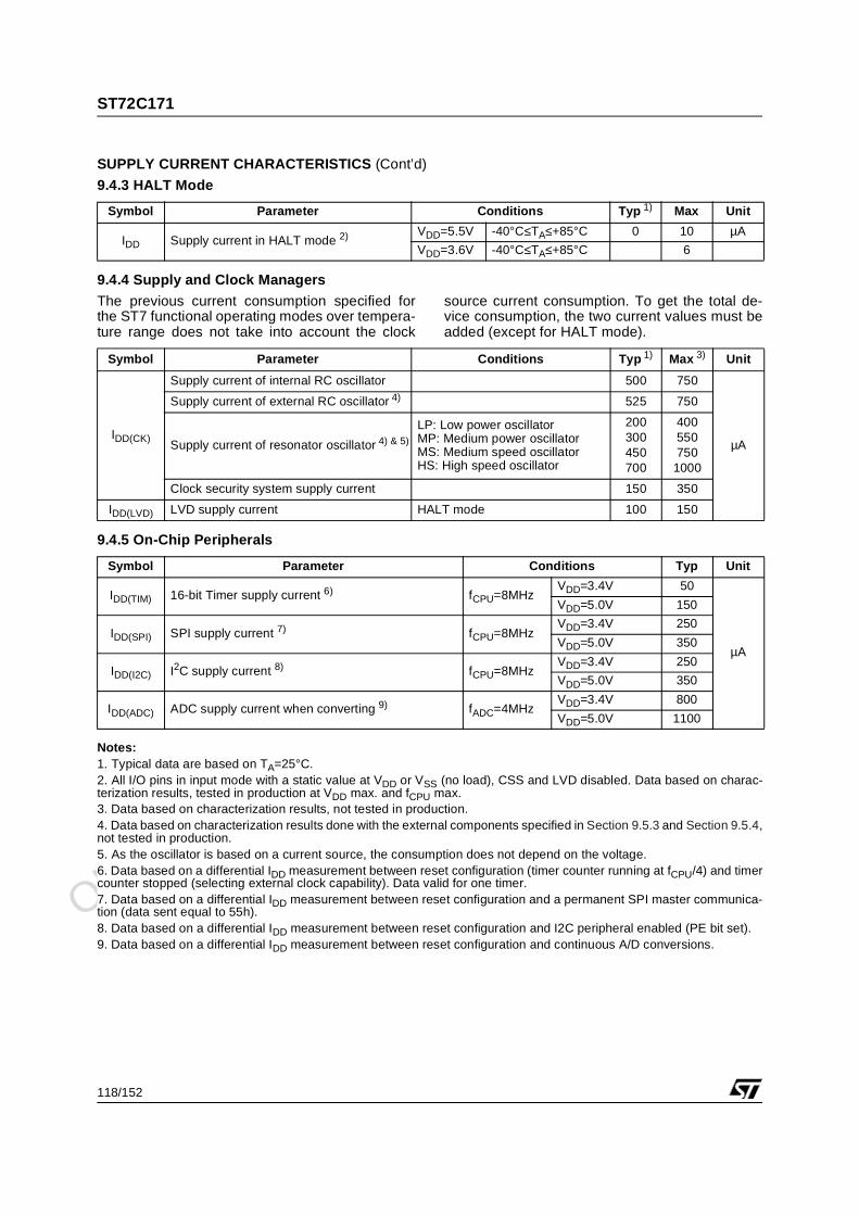
Obsolete Product(
s) - O
bsolete Product(
s)
ST72C171
118/152
SUPPLY CURRENT CHARACTERISTICS (Cont’d)
9.4.3 HALT Mode
9.4.4 Supply and Clock Managers
The previous current consumption specified forthe ST7 functional operating modes over tempera-ture range does not take into account the clock
source current consumption. To get the total de-vice consumption, the two current values must beadded (except for HALT mode).
9.4.5 On-Chip Peripherals
Notes:1. Typical data are based on TA=25°C.2. All I/O pins in input mode with a static value at VDD or VSS (no load), CSS and LVD disabled. Data based on charac-terization results, tested in production at VDD max. and fCPU max.3. Data based on characterization results, not tested in production.4. Data based on characterization results done with the external components specified in Section 9.5.3 and Section 9.5.4,not tested in production.5. As the oscillator is based on a current source, the consumption does not depend on the voltage.6. Data based on a differential IDD measurement between reset configuration (timer counter running at fCPU/4) and timercounter stopped (selecting external clock capability). Data valid for one timer.7. Data based on a differential IDD measurement between reset configuration and a permanent SPI master communica-tion (data sent equal to 55h).8. Data based on a differential IDD measurement between reset configuration and I2C peripheral enabled (PE bit set).9. Data based on a differential IDD measurement between reset configuration and continuous A/D conversions.
Symbol Parameter Conditions Typ 1) Max Unit
IDD Supply current in HALT mode 2) VDD=5.5V -40°C≤TA≤+85°C 0 10 µA
VDD=3.6V -40°C≤TA≤+85°C 6
Symbol Parameter Conditions Typ 1) Max 3) Unit
IDD(CK)
Supply current of internal RC oscillator 500 750
µA
Supply current of external RC oscillator 4) 525 750
Supply current of resonator oscillator 4) & 5)
LP: Low power oscillatorMP: Medium power oscillatorMS: Medium speed oscillatorHS: High speed oscillator
200300450700
400550750
1000
Clock security system supply current 150 350
IDD(LVD) LVD supply current HALT mode 100 150
Symbol Parameter Conditions Typ Unit
IDD(TIM) 16-bit Timer supply current 6) fCPU=8MHzVDD=3.4V 50
µA
VDD=5.0V 150
IDD(SPI) SPI supply current 7) fCPU=8MHzVDD=3.4V 250
VDD=5.0V 350
IDD(I2C) I2C supply current 8) fCPU=8MHzVDD=3.4V 250
VDD=5.0V 350
IDD(ADC) ADC supply current when converting 9) fADC=4MHzVDD=3.4V 800
VDD=5.0V 1100
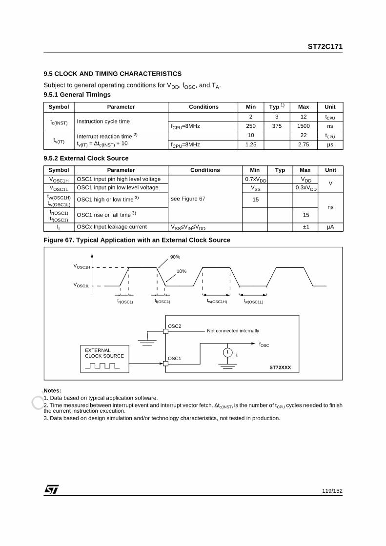
Obsolete Product(
s) - O
bsolete Product(
s)
ST72C171
119/152
9.5 CLOCK AND TIMING CHARACTERISTICS
Subject to general operating conditions for VDD, fOSC, and TA.
9.5.1 General Timings
9.5.2 External Clock Source
Figure 67. Typical Application with an External Clock Source
Notes:1. Data based on typical application software.2. Time measured between interrupt event and interrupt vector fetch. ∆tc(INST) is the number of tCPU cycles needed to finishthe current instruction execution.3. Data based on design simulation and/or technology characteristics, not tested in production.
Symbol Parameter Conditions Min Typ 1) Max Unit
tc(INST) Instruction cycle time2 3 12 tCPU
fCPU=8MHz 250 375 1500 ns
tv(IT)Interrupt reaction time 2)
tv(IT) = ∆tc(INST) + 10
10 22 tCPU
fCPU=8MHz 1.25 2.75 µs
Symbol Parameter Conditions Min Typ Max Unit
VOSC1H OSC1 input pin high level voltage
see Figure 67
0.7xVDD VDD VVOSC1L OSC1 input pin low level voltage VSS 0.3xVDD
tw(OSC1H)tw(OSC1L)
OSC1 high or low time 3) 15ns
tr(OSC1)tf(OSC1)
OSC1 rise or fall time 3) 15
IL OSCx Input leakage current VSS≤VIN≤VDD ±1 µA
OSC1
OSC2
fOSCEXTERNAL
ST72XXX
CLOCK SOURCE
Not connected internally
VOSC1L
VOSC1H
tr(OSC1) tf(OSC1) tw(OSC1H) tw(OSC1L)
IL
90%
10%
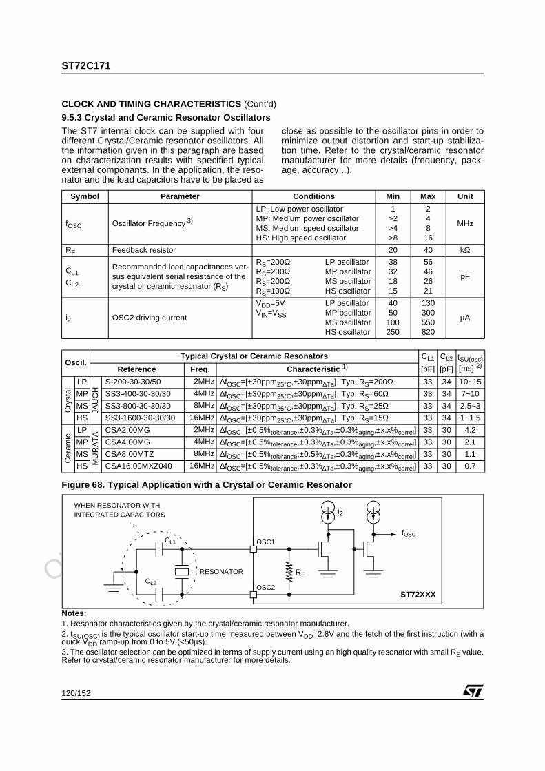
Obsolete Product(
s) - O
bsolete Product(
s)
ST72C171
120/152
CLOCK AND TIMING CHARACTERISTICS (Cont’d)
9.5.3 Crystal and Ceramic Resonator Oscillators
The ST7 internal clock can be supplied with fourdifferent Crystal/Ceramic resonator oscillators. Allthe information given in this paragraph are basedon characterization results with specified typicalexternal componants. In the application, the reso-nator and the load capacitors have to be placed as
close as possible to the oscillator pins in order tominimize output distortion and start-up stabiliza-tion time. Refer to the crystal/ceramic resonatormanufacturer for more details (frequency, pack-age, accuracy...).
Figure 68. Typical Application with a Crystal or Ceramic Resonator
Notes:1. Resonator characteristics given by the crystal/ceramic resonator manufacturer.2. tSU(OSC) is the typical oscillator start-up time measured between VDD=2.8V and the fetch of the first instruction (with aquick VDD ramp-up from 0 to 5V (<50µs).3. The oscillator selection can be optimized in terms of supply current using an high quality resonator with small RS value.Refer to crystal/ceramic resonator manufacturer for more details.
Symbol Parameter Conditions Min Max Unit
fOSC Oscillator Frequency 3)
LP: Low power oscillatorMP: Medium power oscillatorMS: Medium speed oscillatorHS: High speed oscillator
1>2>4>8
24816
MHz
RF Feedback resistor 20 40 kΩ
CL1
CL2
Recommanded load capacitances ver-sus equivalent serial resistance of the crystal or ceramic resonator (RS)
RS=200Ω LP oscillatorRS=200Ω MP oscillatorRS=200Ω MS oscillatorRS=100Ω HS oscillator
38321815
56462621
pF
i2 OSC2 driving current
VDD=5V LP oscillatorVIN=VSS MP oscillator
MS oscillatorHS oscillator
4050
100250
130300550820
µA
Oscil.Typical Crystal or Ceramic Resonators CL1
[pF]
CL2
[pF]
tSU(osc)
[ms] 2)Reference Freq. Characteristic 1)
Cry
stal
LP
JAU
CH
S-200-30-30/50 2MHz ∆fOSC=[±30ppm25°C,±30ppm∆Ta], Typ. RS=200Ω 33 34 10~15
MP SS3-400-30-30/30 4MHz ∆fOSC=[±30ppm25°C,±30ppm∆Ta], Typ. RS=60Ω 33 34 7~10
MS SS3-800-30-30/30 8MHz ∆fOSC=[±30ppm25°C,±30ppm∆Ta], Typ. RS=25Ω 33 34 2.5~3
HS SS3-1600-30-30/30 16MHz ∆fOSC=[±30ppm25°C,±30ppm∆Ta], Typ. RS=15Ω 33 34 1~1.5
Ce
ram
ic
LP
MU
RA
TA CSA2.00MG 2MHz ∆fOSC=[±0.5%tolerance,±0.3%∆Ta,±0.3%aging,±x.x%correl] 33 30 4.2
MP CSA4.00MG 4MHz ∆fOSC=[±0.5%tolerance,±0.3%∆Ta,±0.3%aging,±x.x%correl] 33 30 2.1
MS CSA8.00MTZ 8MHz ∆fOSC=[±0.5%tolerance,±0.5%∆Ta,±0.3%aging,±x.x%correl] 33 30 1.1
HS CSA16.00MXZ040 16MHz ∆fOSC=[±0.5%tolerance,±0.3%∆Ta,±0.3%aging,±x.x%correl] 33 30 0.7
OSC2
OSC1fOSC
CL1
CL2
i2
RF
ST72XXX
RESONATOR
WHEN RESONATOR WITHINTEGRATED CAPACITORS
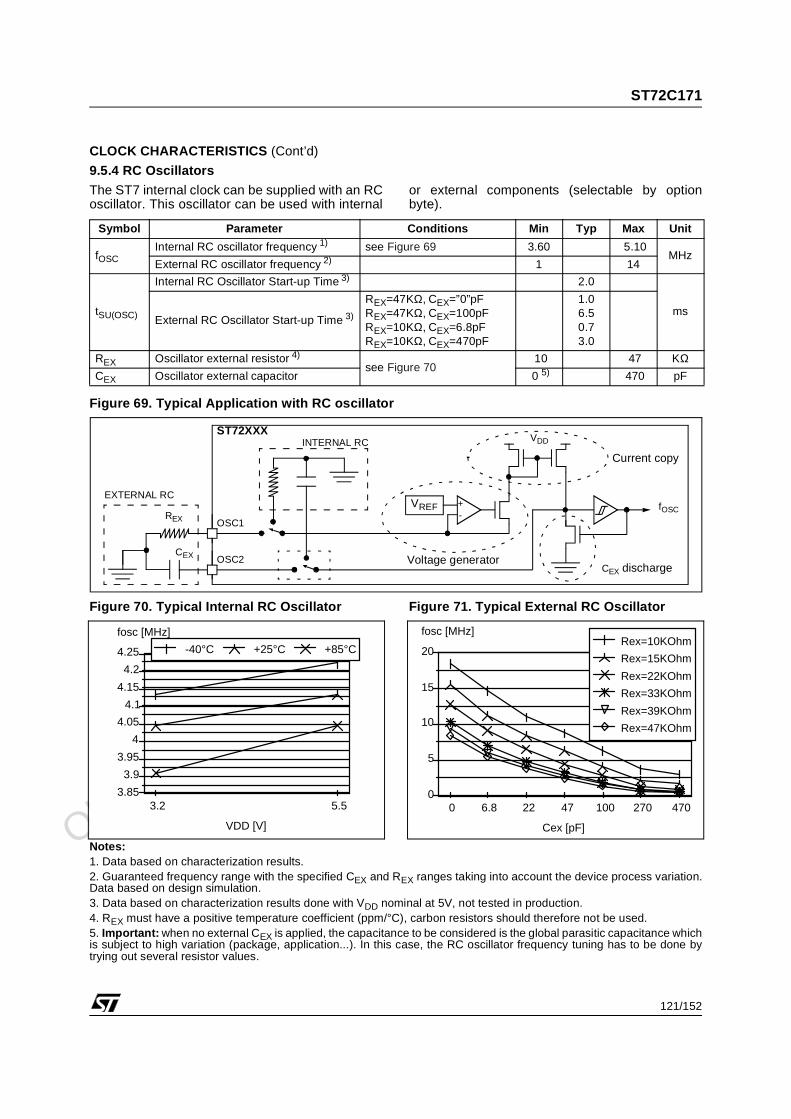
Obsolete Product(
s) - O
bsolete Product(
s)
ST72C171
121/152
CLOCK CHARACTERISTICS (Cont’d)
9.5.4 RC Oscillators
The ST7 internal clock can be supplied with an RCoscillator. This oscillator can be used with internal
or external components (selectable by optionbyte).
Figure 69. Typical Application with RC oscillator
Figure 70. Typical Internal RC Oscillator Figure 71. Typical External RC Oscillator
Notes:1. Data based on characterization results.2. Guaranteed frequency range with the specified CEX and REX ranges taking into account the device process variation.Data based on design simulation.3. Data based on characterization results done with VDD nominal at 5V, not tested in production.4. REX must have a positive temperature coefficient (ppm/°C), carbon resistors should therefore not be used.5. Important: when no external CEX is applied, the capacitance to be considered is the global parasitic capacitance whichis subject to high variation (package, application...). In this case, the RC oscillator frequency tuning has to be done bytrying out several resistor values.
Symbol Parameter Conditions Min Typ Max Unit
fOSCInternal RC oscillator frequency 1) see Figure 69 3.60 5.10
MHzExternal RC oscillator frequency 2) 1 14
tSU(OSC)
Internal RC Oscillator Start-up Time 3) 2.0
msExternal RC Oscillator Start-up Time 3)
REX=47KΩ, CEX=”0”pFREX=47KΩ, CEX=100pFREX=10KΩ, CEX=6.8pFREX=10KΩ, CEX=470pF
1.06.50.73.0
REX Oscillator external resistor 4)
see Figure 7010 47 KΩ
CEX Oscillator external capacitor 0 5) 470 pF
OSC2
OSC1
fOSC
CEX
REX
EXTERNAL RC
INTERNAL RC
VREF +-
VDD
Current copy
Voltage generatorCEX discharge
ST72XXX
3.2 5.5
VDD [V]
3.85
3.9
3.95
4
4.05
4.1
4.15
4.2
4.25
fosc [MHz]
-40°C +25°C +85°C
0 6.8 22 47 100 270 470
Cex [pF]
0
5
10
15
20
fosc [MHz]Rex=10KOhm
Rex=15KOhm
Rex=22KOhm
Rex=33KOhm
Rex=39KOhm
Rex=47KOhm
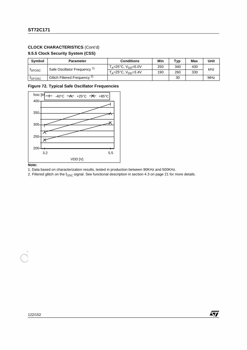
Obsolete Product(
s) - O
bsolete Product(
s)
ST72C171
122/152
CLOCK CHARACTERISTICS (Cont’d)
9.5.5 Clock Security System (CSS)
Figure 72. Typical Safe Oscillator Frequencies
Note:1. Data based on characterization results, tested in production between 90KHz and 500KHz.2. Filtered glitch on the fOSC signal. See functional description in section 4.3 on page 21 for more details.
Symbol Parameter Conditions Min Typ Max Unit
fSFOSC Safe Oscillator Frequency 1) TA=25°C, VDD=5.0V 250 340 430kHz
TA=25°C, VDD=3.4V 190 260 330
fGFOSC Glitch Filtered Frequency 2) 30 MHz
3.2 5.5
VDD [V]
200
250
300
350
400
fosc [kHz] -40°C +25°C +85°C
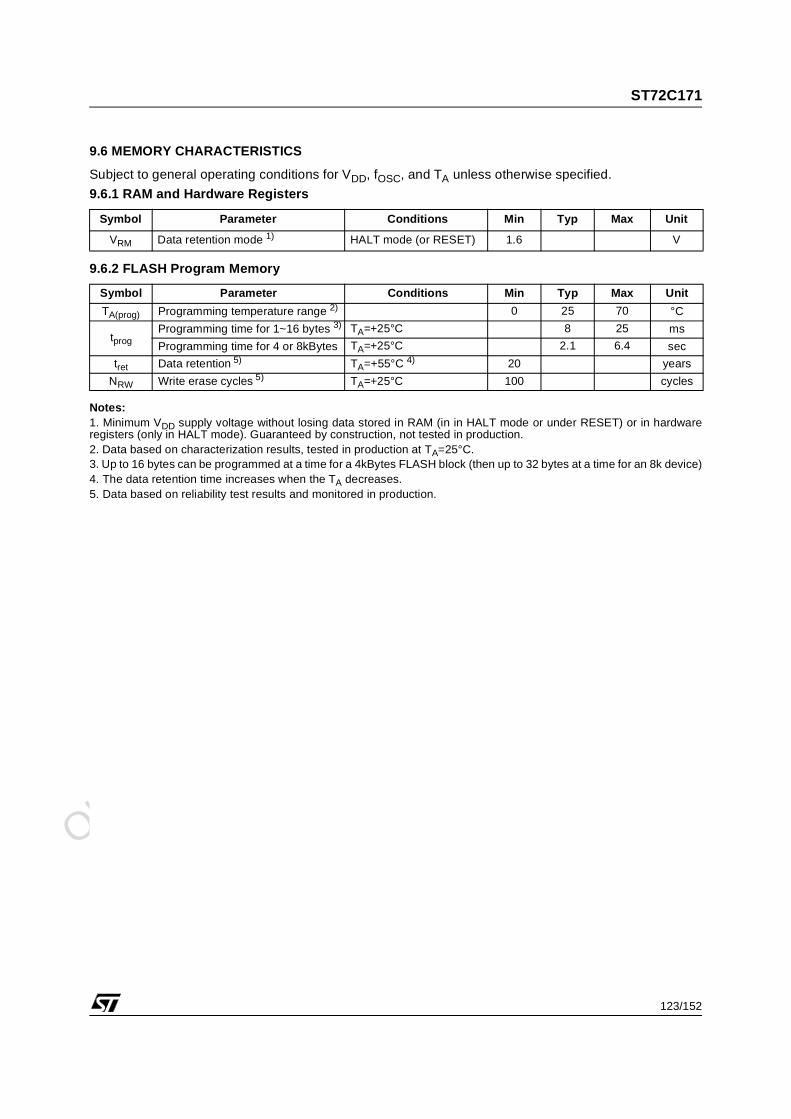
Obsolete Product(
s) - O
bsolete Product(
s)
ST72C171
123/152
9.6 MEMORY CHARACTERISTICS
Subject to general operating conditions for VDD, fOSC, and TA unless otherwise specified.
9.6.1 RAM and Hardware Registers
9.6.2 FLASH Program Memory
Notes:1. Minimum VDD supply voltage without losing data stored in RAM (in in HALT mode or under RESET) or in hardwareregisters (only in HALT mode). Guaranteed by construction, not tested in production.2. Data based on characterization results, tested in production at TA=25°C.3. Up to 16 bytes can be programmed at a time for a 4kBytes FLASH block (then up to 32 bytes at a time for an 8k device)4. The data retention time increases when the TA decreases.5. Data based on reliability test results and monitored in production.
Symbol Parameter Conditions Min Typ Max Unit
VRM Data retention mode 1) HALT mode (or RESET) 1.6 V
Symbol Parameter Conditions Min Typ Max Unit
TA(prog) Programming temperature range 2) 0 25 70 °C
tprogProgramming time for 1~16 bytes 3) TA=+25°C 8 25 ms
Programming time for 4 or 8kBytes TA=+25°C 2.1 6.4 sec
tret Data retention 5) TA=+55°C 4) 20 years
NRW Write erase cycles 5) TA=+25°C 100 cycles
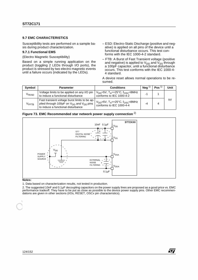
Obsolete Product(
s) - O
bsolete Product(
s)
ST72C171
124/152
9.7 EMC CHARACTERISTICS
Susceptibility tests are performed on a sample ba-sis during product characterization.
9.7.1 Functional EMS
(Electro Magnetic Susceptibility)
Based on a simple running application on theproduct (toggling 2 LEDs through I/O ports), theproduct is stressed by two electro magnetic eventsuntil a failure occurs (indicated by the LEDs).
– ESD: Electro-Static Discharge (positive and neg-ative) is applied on all pins of the device until a functional disturbance occurs. This test con-forms with the IEC 1000-4-2 standard.
– FTB: A Burst of Fast Transient voltage (positive and negative) is applied to VDD and VSS through a 100pF capacitor, until a functional disturbance occurs. This test conforms with the IEC 1000-4-4 standard.
A device reset allows normal operations to be re-sumed.
Figure 73. EMC Recommended star network power supply connection 2)
Notes:1. Data based on characterization results, not tested in production.2. The suggested 10nF and 0.1µF decoupling capacitors on the power supply lines are proposed as a good price vs. EMCperformance tradeoff. They have to be put as close as possible to the device power supply pins. Other EMC recommen-dations are given in other sections (I/Os, RESET, OSCx pin characteristics).
Symbol Parameter Conditions Neg 1) Pos 1) Unit
VFESDVoltage limits to be applied on any I/O pin to induce a functional disturbance
VDD=5V, TA=+25°C, fOSC=8MHzconforms to IEC 1000-4-2
-1 1
kVVFFTB
Fast transient voltage burst limits to be ap-plied through 100pF on VDD and VDD pins to induce a functional disturbance
VDD=5V, TA=+25°C, fOSC=8MHzconforms to IEC 1000-4-4
-4 4
VDD
VSS
0.1µF10nF
VDD
ST72XXX
VSSA
VDDA
0.1µF
POWERSUPPLYSOURCE
ST7DIGITAL NOISEFILTERING
EXTERNALNOISEFILTERING
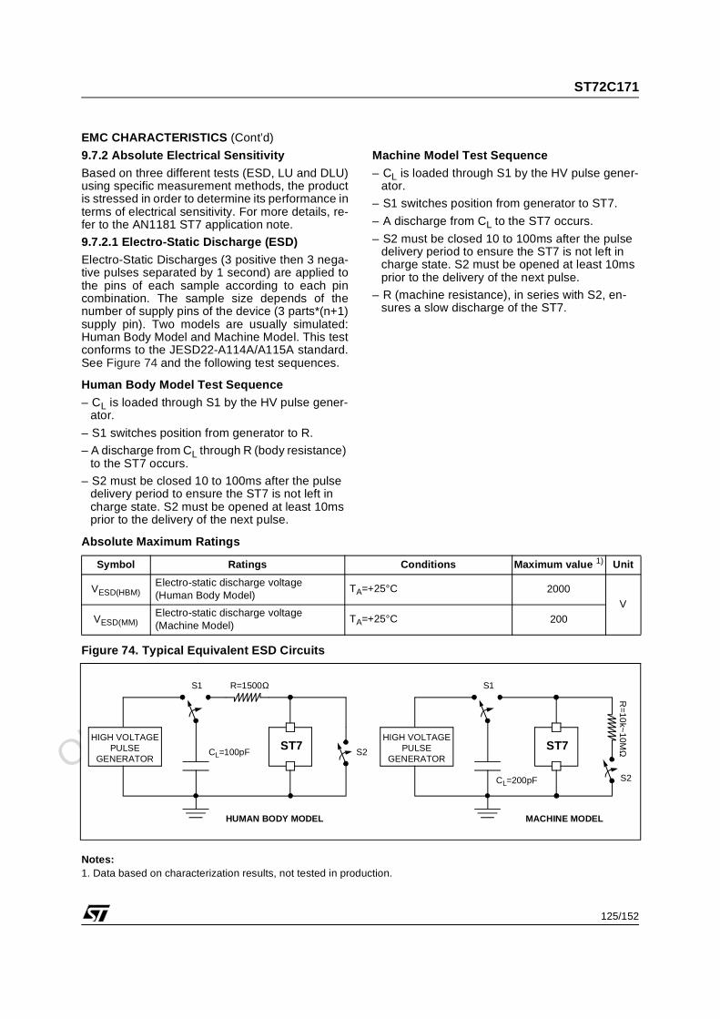
Obsolete Product(
s) - O
bsolete Product(
s)
ST72C171
125/152
EMC CHARACTERISTICS (Cont’d)
9.7.2 Absolute Electrical Sensitivity
Based on three different tests (ESD, LU and DLU)using specific measurement methods, the productis stressed in order to determine its performance interms of electrical sensitivity. For more details, re-fer to the AN1181 ST7 application note.
9.7.2.1 Electro-Static Discharge (ESD)
Electro-Static Discharges (3 positive then 3 nega-tive pulses separated by 1 second) are applied tothe pins of each sample according to each pincombination. The sample size depends of thenumber of supply pins of the device (3 parts*(n+1)supply pin). Two models are usually simulated:Human Body Model and Machine Model. This testconforms to the JESD22-A114A/A115A standard.See Figure 74 and the following test sequences.
Human Body Model Test Sequence
– CL is loaded through S1 by the HV pulse gener-ator.
– S1 switches position from generator to R.
– A discharge from CL through R (body resistance) to the ST7 occurs.
– S2 must be closed 10 to 100ms after the pulse delivery period to ensure the ST7 is not left in charge state. S2 must be opened at least 10ms prior to the delivery of the next pulse.
Machine Model Test Sequence
– CL is loaded through S1 by the HV pulse gener-ator.
– S1 switches position from generator to ST7.
– A discharge from CL to the ST7 occurs.
– S2 must be closed 10 to 100ms after the pulse delivery period to ensure the ST7 is not left in charge state. S2 must be opened at least 10ms prior to the delivery of the next pulse.
– R (machine resistance), in series with S2, en-sures a slow discharge of the ST7.
Absolute Maximum Ratings
Figure 74. Typical Equivalent ESD Circuits
Notes:1. Data based on characterization results, not tested in production.
Symbol Ratings Conditions Maximum value 1) Unit
VESD(HBM)Electro-static discharge voltage(Human Body Model)
TA=+25°C 2000
V
VESD(MM)Electro-static discharge voltage(Machine Model)
TA=+25°C 200
ST7S2
R=1500ΩS1
HIGH VOLTAGE
CL=100pFPULSEGENERATOR
ST7
S2
HIGH VOLTAGE
CL=200pF
PULSEGENERATOR
R=
10k~
10MΩ
S1
HUMAN BODY MODEL MACHINE MODEL
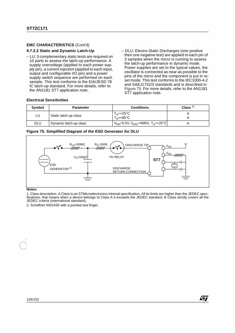
Obsolete Product(
s) - O
bsolete Product(
s)
ST72C171
126/152
EMC CHARACTERISTICS (Cont’d)
9.7.2.2 Static and Dynamic Latch-Up
– LU: 3 complementary static tests are required on 10 parts to assess the latch-up performance. A supply overvoltage (applied to each power sup-ply pin), a current injection (applied to each input, output and configurable I/O pin) and a power supply switch sequence are performed on each sample. This test conforms to the EIA/JESD 78 IC latch-up standard. For more details, refer to the AN1181 ST7 application note.
– DLU: Electro-Static Discharges (one positive then one negative test) are applied to each pin of 3 samples when the micro is running to assess the latch-up performance in dynamic mode. Power supplies are set to the typical values, the oscillator is connected as near as possible to the pins of the micro and the component is put in re-set mode. This test conforms to the IEC1000-4-2 and SAEJ1752/3 standards and is described in Figure 75. For more details, refer to the AN1181 ST7 application note.
Electrical Sensitivities
Figure 75. Simplified Diagram of the ESD Generator for DLU
Notes:1. Class description: A Class is an STMicroelectronics internal specification. All its limits are higher than the JEDEC spec-ifications, that means when a device belongs to Class A it exceeds the JEDEC standard. B Class strictly covers all theJEDEC criteria (international standard).2. Schaffner NSG435 with a pointed test finger.
Symbol Parameter Conditions Class 1)
LU Static latch-up classTA=+25°CTA=+85°C
AA
DLU Dynamic latch-up class VDD=5.5V, fOSC=4MHz, TA=+25°C A
RCH=50MΩ RD=330Ω
CS=150pF
ESD
HV RELAY
DISCHARGE TIP
DISCHARGERETURN CONNECTION
GENERATOR 2)
ST7
VDD
VSS
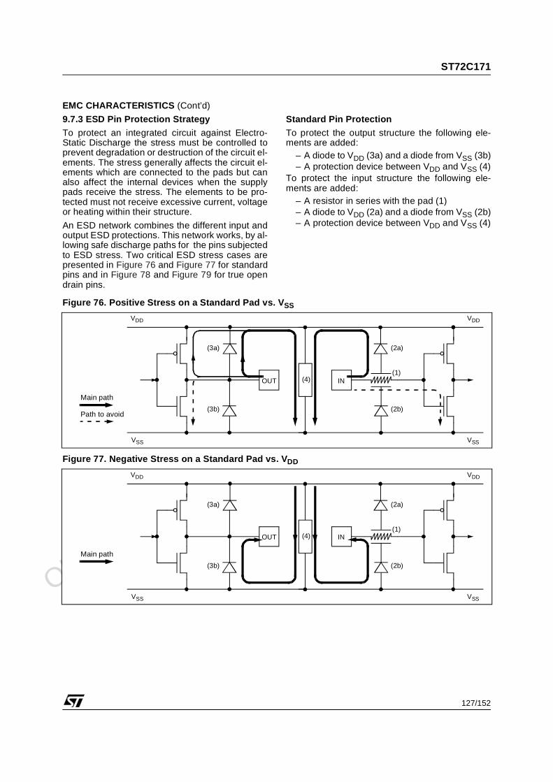
Obsolete Product(
s) - O
bsolete Product(
s)
ST72C171
127/152
EMC CHARACTERISTICS (Cont’d)
9.7.3 ESD Pin Protection Strategy
To protect an integrated circuit against Electro-Static Discharge the stress must be controlled toprevent degradation or destruction of the circuit el-ements. The stress generally affects the circuit el-ements which are connected to the pads but canalso affect the internal devices when the supplypads receive the stress. The elements to be pro-tected must not receive excessive current, voltageor heating within their structure.
An ESD network combines the different input andoutput ESD protections. This network works, by al-lowing safe discharge paths for the pins subjectedto ESD stress. Two critical ESD stress cases arepresented in Figure 76 and Figure 77 for standardpins and in Figure 78 and Figure 79 for true opendrain pins.
Standard Pin Protection
To protect the output structure the following ele-ments are added:
– A diode to VDD (3a) and a diode from VSS (3b)– A protection device between VDD and VSS (4)
To protect the input structure the following ele-ments are added:
– A resistor in series with the pad (1)– A diode to VDD (2a) and a diode from VSS (2b)– A protection device between VDD and VSS (4)
Figure 76. Positive Stress on a Standard Pad vs. VSS
Figure 77. Negative Stress on a Standard Pad vs. VDD
IN
VDD
VSS
(1)
(2a)
(2b)
(4)OUT
VDD
VSS
(3a)
(3b)
Main path
Path to avoid
IN
VDD
VSS
(1)
(2a)
(2b)
(4)OUT
VDD
VSS
(3a)
(3b)
Main path
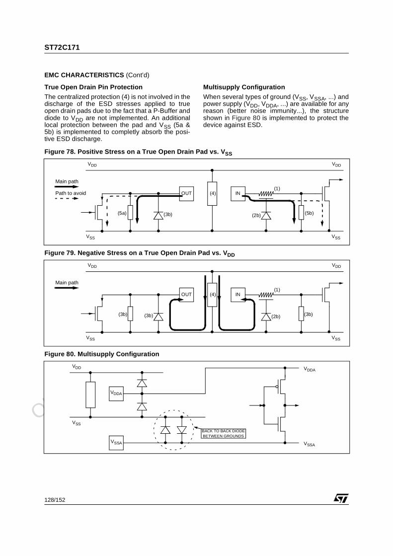
Obsolete Product(
s) - O
bsolete Product(
s)
ST72C171
128/152
EMC CHARACTERISTICS (Cont’d)
True Open Drain Pin Protection
The centralized protection (4) is not involved in thedischarge of the ESD stresses applied to trueopen drain pads due to the fact that a P-Buffer anddiode to VDD are not implemented. An additionallocal protection between the pad and VSS (5a &5b) is implemented to completly absorb the posi-tive ESD discharge.
Multisupply Configuration
When several types of ground (VSS, VSSA, ...) andpower supply (VDD, VDDA, ...) are available for anyreason (better noise immunity...), the structureshown in Figure 80 is implemented to protect thedevice against ESD.
Figure 78. Positive Stress on a True Open Drain Pad vs. VSS
Figure 79. Negative Stress on a True Open Drain Pad vs. VDD
Figure 80. Multisupply Configuration
IN
VDD
VSS
(1)
(2b)
(4)OUT
VDD
VSS
(3b)
Main path
Path to avoid
(5a) (5b)
IN
VDD
VSS
(1)
(2b)
(4)OUT
VDD
VSS
(3b)
Main path
(3b) (3b)
VDDA
VSSA
VDDA
VDD
VSS
BACK TO BACK DIODEBETWEEN GROUNDS
VSSA
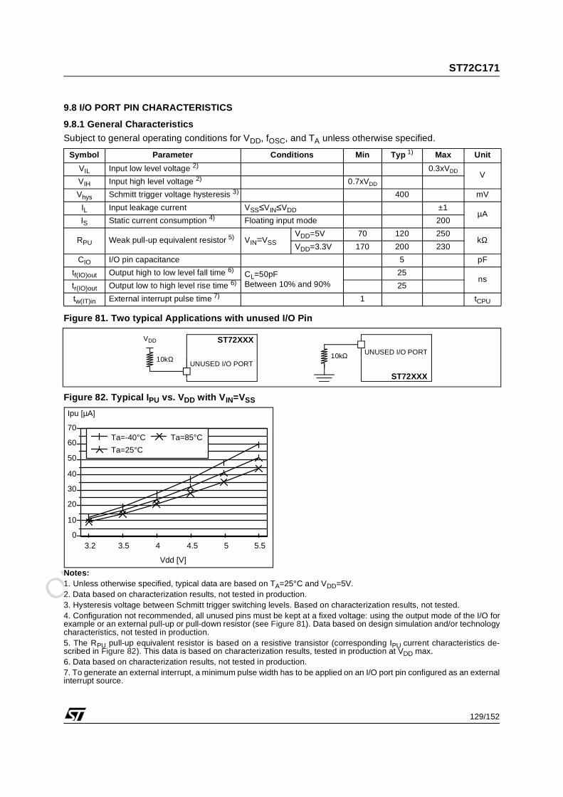
Obsolete Product(
s) - O
bsolete Product(
s)
ST72C171
129/152
9.8 I/O PORT PIN CHARACTERISTICS
9.8.1 General Characteristics
Subject to general operating conditions for VDD, fOSC, and TA unless otherwise specified.
Figure 81. Two typical Applications with unused I/O Pin
Figure 82. Typical IPU vs. VDD with VIN=VSS
Notes:1. Unless otherwise specified, typical data are based on TA=25°C and VDD=5V.2. Data based on characterization results, not tested in production.3. Hysteresis voltage between Schmitt trigger switching levels. Based on characterization results, not tested.4. Configuration not recommended, all unused pins must be kept at a fixed voltage: using the output mode of the I/O forexample or an external pull-up or pull-down resistor (see Figure 81). Data based on design simulation and/or technologycharacteristics, not tested in production.5. The RPU pull-up equivalent resistor is based on a resistive transistor (corresponding IPU current characteristics de-scribed in Figure 82). This data is based on characterization results, tested in production at VDD max.6. Data based on characterization results, not tested in production.7. To generate an external interrupt, a minimum pulse width has to be applied on an I/O port pin configured as an externalinterrupt source.
Symbol Parameter Conditions Min Typ 1) Max Unit
VIL Input low level voltage 2) 0.3xVDD VVIH Input high level voltage 2) 0.7xVDD
Vhys Schmitt trigger voltage hysteresis 3) 400 mV
IL Input leakage current VSS≤VIN≤VDD ±1µA
IS Static current consumption 4) Floating input mode 200
RPU Weak pull-up equivalent resistor 5) VIN=VSSVDD=5V 70 120 250
kΩVDD=3.3V 170 200 230
CIO I/O pin capacitance 5 pF
tf(IO)out Output high to low level fall time 6)CL=50pFBetween 10% and 90%
25ns
tr(IO)out Output low to high level rise time 6) 25
tw(IT)in External interrupt pulse time 7) 1 tCPU
10kΩ UNUSED I/O PORT
ST72XXX
10kΩUNUSED I/O PORT
ST72XXXVDD
3.2 3.5 4 4.5 5 5.5
Vdd [V]
0
10
20
30
40
50
60
70
Ipu [µA]
Ta=-40°C
Ta=25°C
Ta=85°C
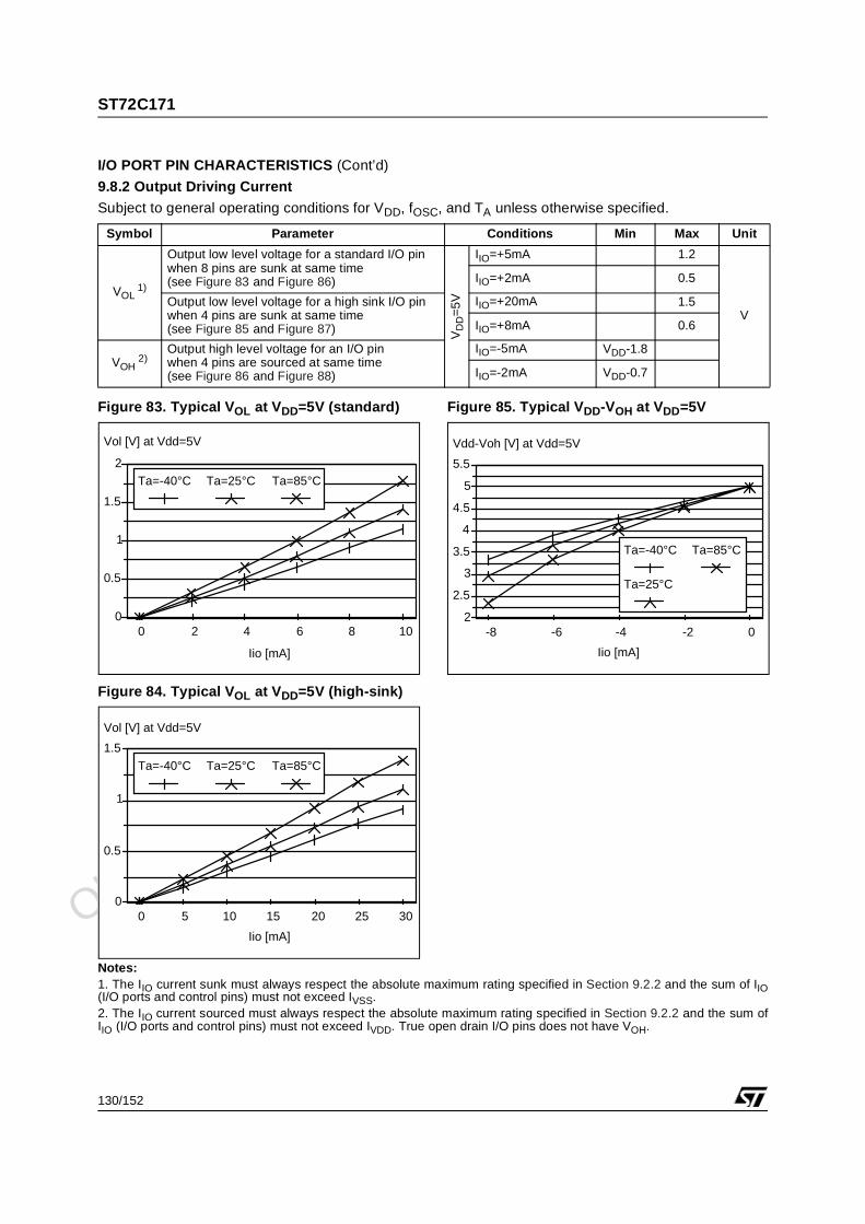
Obsolete Product(
s) - O
bsolete Product(
s)
ST72C171
130/152
I/O PORT PIN CHARACTERISTICS (Cont’d)
9.8.2 Output Driving Current
Subject to general operating conditions for VDD, fOSC, and TA unless otherwise specified.
Figure 83. Typical VOL at VDD=5V (standard)
Figure 84. Typical VOL at VDD=5V (high-sink)
Figure 85. Typical VDD-VOH at VDD=5V
Notes:1. The IIO current sunk must always respect the absolute maximum rating specified in Section 9.2.2 and the sum of IIO(I/O ports and control pins) must not exceed IVSS.2. The IIO current sourced must always respect the absolute maximum rating specified in Section 9.2.2 and the sum ofIIO (I/O ports and control pins) must not exceed IVDD. True open drain I/O pins does not have VOH.
Symbol Parameter Conditions Min Max Unit
VOL 1)
Output low level voltage for a standard I/O pin when 8 pins are sunk at same time(see Figure 83 and Figure 86)
VD
D=
5V
IIO=+5mA 1.2
V
IIO=+2mA 0.5
Output low level voltage for a high sink I/O pin when 4 pins are sunk at same time(see Figure 85 and Figure 87)
IIO=+20mA 1.5
IIO=+8mA 0.6
VOH 2)
Output high level voltage for an I/O pinwhen 4 pins are sourced at same time(see Figure 86 and Figure 88)
IIO=-5mA VDD-1.8
IIO=-2mA VDD-0.7
0 2 4 6 8 10
Iio [mA]
0
0.5
1
1.5
2
Vol [V] at Vdd=5V
Ta=-40°C Ta=25°C Ta=85°C
0 5 10 15 20 25 30
Iio [mA]
0
0.5
1
1.5
Vol [V] at Vdd=5V
Ta=-40°C Ta=25°C Ta=85°C
-8 -6 -4 -2 0
Iio [mA]
2
2.5
3
3.5
4
4.5
5
5.5
Vdd-Voh [V] at Vdd=5V
Ta=-40°C
Ta=25°C
Ta=85°C
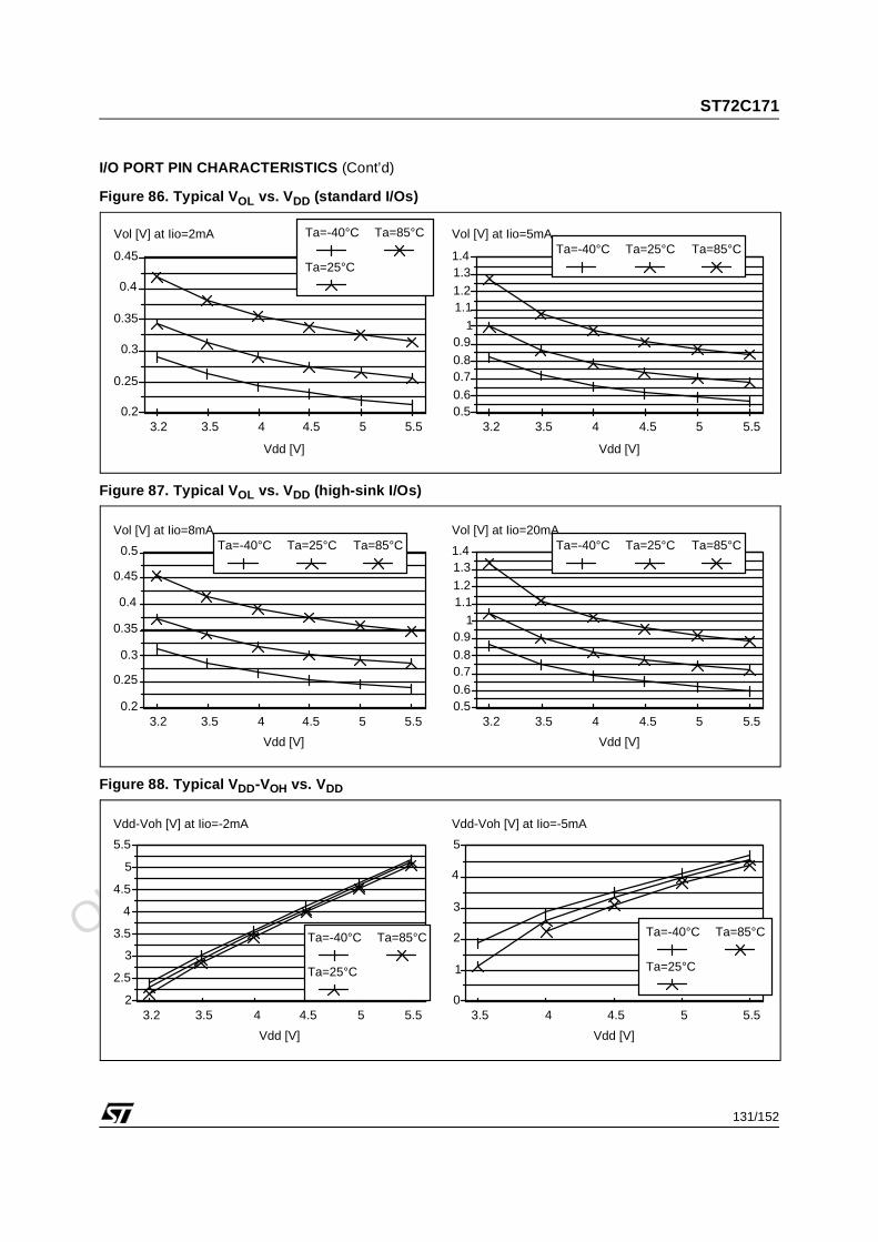
Obsolete Product(
s) - O
bsolete Product(
s)
ST72C171
131/152
I/O PORT PIN CHARACTERISTICS (Cont’d)
Figure 86. Typical VOL vs. VDD (standard I/Os)
Figure 87. Typical VOL vs. VDD (high-sink I/Os)
Figure 88. Typical VDD-VOH vs. VDD
3.2 3.5 4 4.5 5 5.5
Vdd [V]
0.2
0.25
0.3
0.35
0.4
0.45
Vol [V] at Iio=2mA Ta=-40°C
Ta=25°C
Ta=85°C
3.2 3.5 4 4.5 5 5.5
Vdd [V]
0.50.6
0.70.8
0.91
1.11.2
1.31.4
Vol [V] at Iio=5mATa=-40°C Ta=25°C Ta=85°C
3.2 3.5 4 4.5 5 5.5
Vdd [V]
0.2
0.25
0.3
0.35
0.4
0.45
0.5
Vol [V] at Iio=8mATa=-40°C Ta=25°C Ta=85°C
3.2 3.5 4 4.5 5 5.5
Vdd [V]
0.50.6
0.70.8
0.91
1.11.2
1.31.4
Vol [V] at Iio=20mATa=-40°C Ta=25°C Ta=85°C
3.5 4 4.5 5 5.5
Vdd [V]
0
1
2
3
4
5
Vdd-Voh [V] at Iio=-5mA
Ta=-40°C
Ta=25°C
Ta=85°C
3.2 3.5 4 4.5 5 5.5
Vdd [V]
2
2.5
3
3.5
4
4.5
5
5.5
Vdd-Voh [V] at Iio=-2mA
Ta=-40°C
Ta=25°C
Ta=85°C
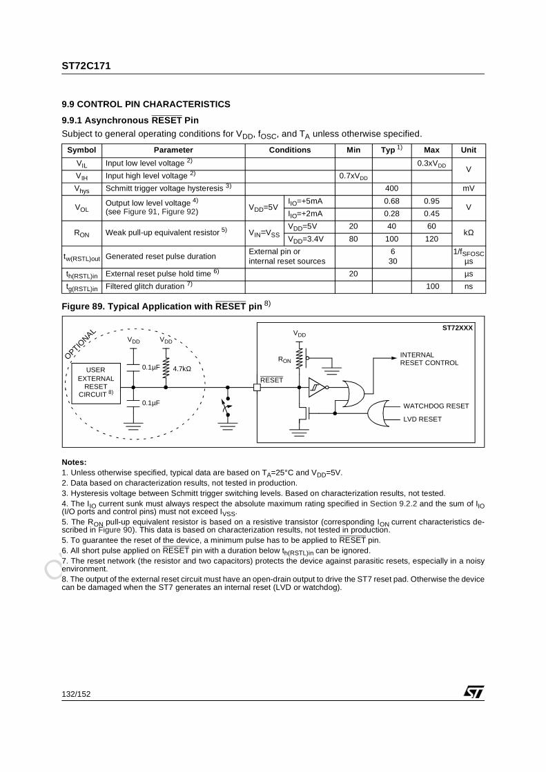
Obsolete Product(
s) - O
bsolete Product(
s)
ST72C171
132/152
9.9 CONTROL PIN CHARACTERISTICS
9.9.1 Asynchronous RESET Pin
Subject to general operating conditions for VDD, fOSC, and TA unless otherwise specified.
Figure 89. Typical Application with RESET pin 8)
Notes:1. Unless otherwise specified, typical data are based on TA=25°C and VDD=5V.2. Data based on characterization results, not tested in production.3. Hysteresis voltage between Schmitt trigger switching levels. Based on characterization results, not tested.4. The IIO current sunk must always respect the absolute maximum rating specified in Section 9.2.2 and the sum of IIO(I/O ports and control pins) must not exceed IVSS.5. The RON pull-up equivalent resistor is based on a resistive transistor (corresponding ION current characteristics de-scribed in Figure 90). This data is based on characterization results, not tested in production.5. To guarantee the reset of the device, a minimum pulse has to be applied to RESET pin.6. All short pulse applied on RESET pin with a duration below th(RSTL)in can be ignored.7. The reset network (the resistor and two capacitors) protects the device against parasitic resets, especially in a noisyenvironment.8. The output of the external reset circuit must have an open-drain output to drive the ST7 reset pad. Otherwise the devicecan be damaged when the ST7 generates an internal reset (LVD or watchdog).
Symbol Parameter Conditions Min Typ 1) Max Unit
VIL Input low level voltage 2) 0.3xVDD VVIH Input high level voltage 2) 0.7xVDD
Vhys Schmitt trigger voltage hysteresis 3) 400 mV
VOLOutput low level voltage 4)
(see Figure 91, Figure 92) VDD=5VIIO=+5mA 0.68 0.95
VIIO=+2mA 0.28 0.45
RON Weak pull-up equivalent resistor 5) VIN=VSSVDD=5V 20 40 60
kΩVDD=3.4V 80 100 120
tw(RSTL)out Generated reset pulse durationExternal pin orinternal reset sources
630
1/fSFOSCµs
th(RSTL)in External reset pulse hold time 6) 20 µs
tg(RSTL)in Filtered glitch duration 7) 100 ns
RESET
VDD
WATCHDOG RESET
ST72XXX
LVD RESET
INTERNALRON
0.1µF
VDD
0.1µF
VDD
4.7kΩEXTERNAL
RESETCIRCUIT 8)
RESET CONTROLOPTIO
NAL
USER
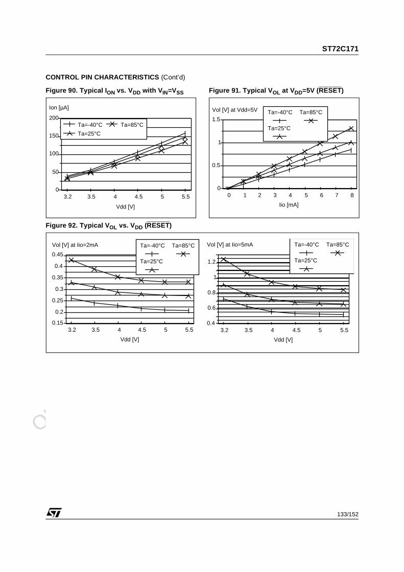
Obsolete Product(
s) - O
bsolete Product(
s)
ST72C171
133/152
CONTROL PIN CHARACTERISTICS (Cont’d)
Figure 90. Typical ION vs. VDD with VIN=VSS Figure 91. Typical VOL at VDD=5V (RESET)
Figure 92. Typical VOL vs. VDD (RESET)
3.2 3.5 4 4.5 5 5.5
Vdd [V]
0
50
100
150
200
Ion [µA]
Ta=-40°C
Ta=25°C
Ta=85°C
0 1 2 3 4 5 6 7 8
Iio [mA]
0
0.5
1
1.5
Vol [V] at Vdd=5V Ta=-40°C
Ta=25°C
Ta=85°C
3.2 3.5 4 4.5 5 5.5
Vdd [V]
0.15
0.2
0.25
0.3
0.35
0.4
0.45
Vol [V] at Iio=2mA Ta=-40°C
Ta=25°C
Ta=85°C
3.2 3.5 4 4.5 5 5.5
Vdd [V]
0.4
0.6
0.8
1
1.2
Vol [V] at Iio=5mA Ta=-40°C
Ta=25°C
Ta=85°C
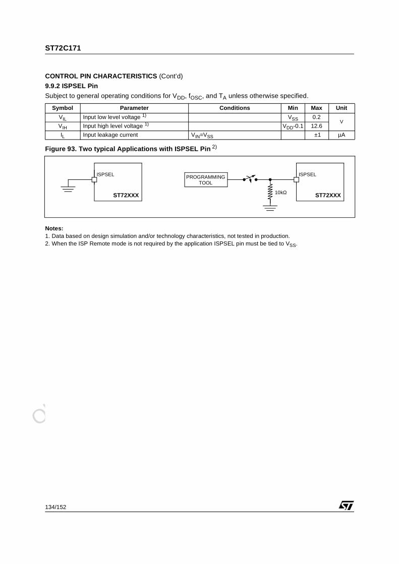
Obsolete Product(
s) - O
bsolete Product(
s)
ST72C171
134/152
CONTROL PIN CHARACTERISTICS (Cont’d)
9.9.2 ISPSEL Pin
Subject to general operating conditions for VDD, fOSC, and TA unless otherwise specified.
Figure 93. Two typical Applications with ISPSEL Pin 2)
Notes:1. Data based on design simulation and/or technology characteristics, not tested in production.2. When the ISP Remote mode is not required by the application ISPSEL pin must be tied to VSS.
Symbol Parameter Conditions Min Max Unit
VIL Input low level voltage 1) VSS 0.2V
VIH Input high level voltage 1) VDD-0.1 12.6
IL Input leakage current VIN=VSS ±1 µA
ISPSEL
ST72XXX 10kΩ
PROGRAMMINGTOOL
ISPSEL
ST72XXX
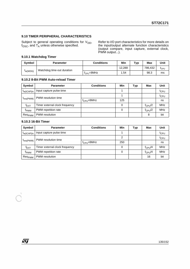
Obsolete Product(
s) - O
bsolete Product(
s)
ST72C171
135/152
9.10 TIMER PERIPHERAL CHARACTERISTICS
Subject to general operating conditions for VDD,fOSC, and TA unless otherwise specified.
Refer to I/O port characteristics for more details onthe input/output alternate function characteristics(output compare, input capture, external clock,PWM output...).
9.10.1 Watchdog Timer
9.10.2 8-Bit PWM Auto-reload Timer
9.10.3 16-Bit Timer
Symbol Parameter Conditions Min Typ Max Unit
tw(WDG) Watchdog time-out duration12,288 786,432 tCPU
fCPU=8MHz 1.54 98.3 ms
Symbol Parameter Conditions Min Typ Max Unit
tw(ICAP)in Input capture pulse time 1 tCPU
tres(PWM) PWM resolution time1 tCPU
fCPU=8MHz 125 ns
fEXT Timer external clock frequency 0 fCPU/2 MHz
fPWM PWM repetition rate 0 fCPU/2 MHz
ResPWM PWM resolution 8 bit
Symbol Parameter Conditions Min Typ Max Unit
tw(ICAP)in Input capture pulse time 1 tCPU
tres(PWM) PWM resolution time2 tCPU
fCPU=8MHz 250 ns
fEXT Timer external clock frequency 0 fCPU/4 MHz
fPWM PWM repetition rate 0 fCPU/4 MHz
ResPWM PWM resolution 16 bit
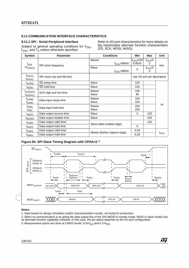
Obsolete Product(
s) - O
bsolete Product(
s)
ST72C171
136/152
9.11 COMMUNICATION INTERFACE CHARACTERISTICS
9.11.1 SPI - Serial Peripheral Interface
Subject to general operating conditions for VDD,fOSC, and TA unless otherwise specified.
Refer to I/O port characteristics for more details onthe input/output alternate function characteristics(SS, SCK, MOSI, MISO).
Figure 94. SPI Slave Timing Diagram with CPHA=0 3)
Notes:1. Data based on design simulation and/or characterisation results, not tested in production.2. When no communication is on-going the data output line of the SPI (MOSI in master mode, MISO in slave mode) hasits alternate function capability released. In this case, the pin status depends on the I/O port configuration.3. Measurement points are done at CMOS levels: 0.3xVDD and 0.7xVDD.
Symbol Parameter Conditions Min Max Unit
fSCK1/tc(SCK)
SPI clock frequency
MasterfCPU=8MHz
fCPU/1280.0625
fCPU/42
MHzSlave
fCPU=8MHz0
fCPU/24
tr(SCK)tf(SCK)
SPI clock rise and fall time see I/O port pin description
tsu(SS) SS setup time Slave 120
ns
th(SS) SS hold time Slave 120
tw(SCKH)tw(SCKL)
SCK high and low timeMasterSlave
10090
tsu(MI)tsu(SI)
Data input setup timeMasterSlave
100100
th(MI)th(SI)
Data input hold timeMasterSlave
100100
ta(SO) Data output access time Slave 0 120
tdis(SO) Data output disable time Slave 240
tv(SO) Data output valid timeSlave (after enable edge)
120
th(SO) Data output hold time 0
tv(MO) Data output valid timeMaster (before capture edge)
0.25tCPUth(MO) Data output hold time 0.25
SS INPUT
SC
KIN
PU
T CPHA=0
MOSI INPUT
MISO OUTPUT
CPHA=0
tc(SCK)
tw(SCKH)tw(SCKL) tr(SCK)
tf(SCK)
tv(SO)ta(SO)
tsu(SI) th(SI)
MSB OUT
MSB IN
BIT6 OUT
LSB IN
LSB OUTsee note 2
CPOL=0
CPOL=1
tsu(SS) th(SS)
tdis(SO)th(SO)
seenote 2
BIT1 IN
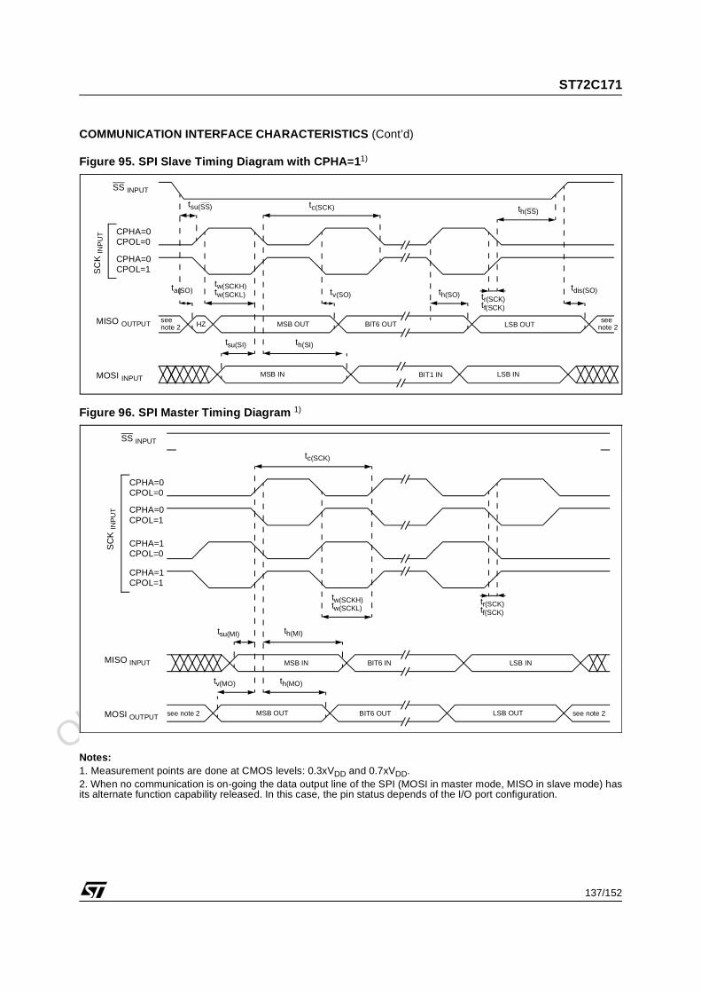
Obsolete Product(
s) - O
bsolete Product(
s)
ST72C171
137/152
COMMUNICATION INTERFACE CHARACTERISTICS (Cont’d)
Figure 95. SPI Slave Timing Diagram with CPHA=11)
Figure 96. SPI Master Timing Diagram 1)
Notes:1. Measurement points are done at CMOS levels: 0.3xVDD and 0.7xVDD.2. When no communication is on-going the data output line of the SPI (MOSI in master mode, MISO in slave mode) hasits alternate function capability released. In this case, the pin status depends of the I/O port configuration.
SS INPUT
SC
KIN
PU
T CPHA=0
MOSI INPUT
MISO OUTPUT
CPHA=0
tw(SCKH)tw(SCKL) tr(SCK)
tf(SCK)
ta(SO)
tsu(SI) th(SI)
MSB OUT BIT6 OUT LSB OUTsee
CPOL=0
CPOL=1
tsu(SS) th(SS)
tdis(SO)th(SO)
seenote 2note 2
tc(SCK)
HZ
tv(SO)
MSB IN LSB INBIT1 IN
SS INPUT
SC
KIN
PU
T
CPHA=0
MOSI OUTPUT
MISO INPUT
CPHA=0
CPHA=1
CPHA=1
tc(SCK)
tw(SCKH)tw(SCKL)
th(MI)tsu(MI)
tv(MO) th(MO)
MSB IN
MSB OUT
BIT6 IN
BIT6 OUT LSB OUT
LSB IN
see note 2 see note 2
CPOL=0
CPOL=1
CPOL=0
CPOL=1
tr(SCK)tf(SCK)
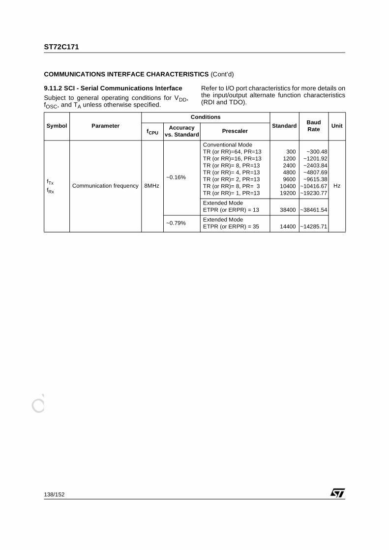
Obsolete Product(
s) - O
bsolete Product(
s)
ST72C171
138/152
COMMUNICATIONS INTERFACE CHARACTERISTICS (Cont’d)
9.11.2 SCI - Serial Communications Interface
Subject to general operating conditions for VDD,fOSC, and TA unless otherwise specified.
Refer to I/O port characteristics for more details onthe input/output alternate function characteristics(RDI and TDO).
Symbol Parameter
Conditions
StandardBaudRate
UnitfCPU
Accuracy vs. Standard
Prescaler
fTx
fRxCommunication frequency 8MHz
~0.16%
Conventional ModeTR (or RR)=64, PR=13TR (or RR)=16, PR=13TR (or RR)= 8, PR=13TR (or RR)= 4, PR=13TR (or RR)= 2, PR=13TR (or RR)= 8, PR= 3TR (or RR)= 1, PR=13
3001200240048009600
1040019200
~300.48~1201.92~2403.84~4807.69~9615.38
~10416.67~19230.77
Hz
Extended ModeETPR (or ERPR) = 13 38400 ~38461.54
~0.79%Extended ModeETPR (or ERPR) = 35 14400 ~14285.71
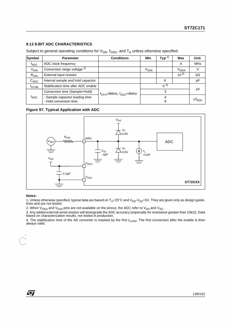
Obsolete Product(
s) - O
bsolete Product(
s)
ST72C171
139/152
9.12 8-BIT ADC CHARACTERISTICS
Subject to general operating conditions for VDD, fOSC, and TA unless otherwise specified.
Figure 97. Typical Application with ADC
Notes:1. Unless otherwise specified, typical data are based on TA=25°C and VDD-VSS=5V. They are given only as design guide-lines and are not tested.2. When VDDA and VSSA pins are not available on the pinout, the ADC refer to VDD and VSS .3. Any added external serial resistor will downgrade the ADC accuracy (especially for resistance greater than 10kΩ). Databased on characterization results, not tested in production.4. The stabilization time of the AD converter is masked by the first tLOAD. The first conversion after the enable is thenalways valid.
Symbol Parameter Conditions Min Typ 1) Max Unit
fADC ADC clock frequency 4 MHz
VAIN Conversion range voltage 2) VSSA VDDA V
RAIN External input resistor 10 3) kΩ
CADC Internal sample and hold capacitor 6 pF
tSTAB Stabilization time after ADC enable
fCPU=8MHz, fADC=4MHz
0 4)
µs
tADC
Conversion time (Sample+Hold) 3
- Sample capacitor loading time- Hold conversion time
48
1/fADC
AINx
ST72XXX
CIO~2pF
VDD
IL±1µA
VT0.6V
VT0.6V
VAIN
RAIN
VDDA
VSSA
0.1µF
VDD
ADC
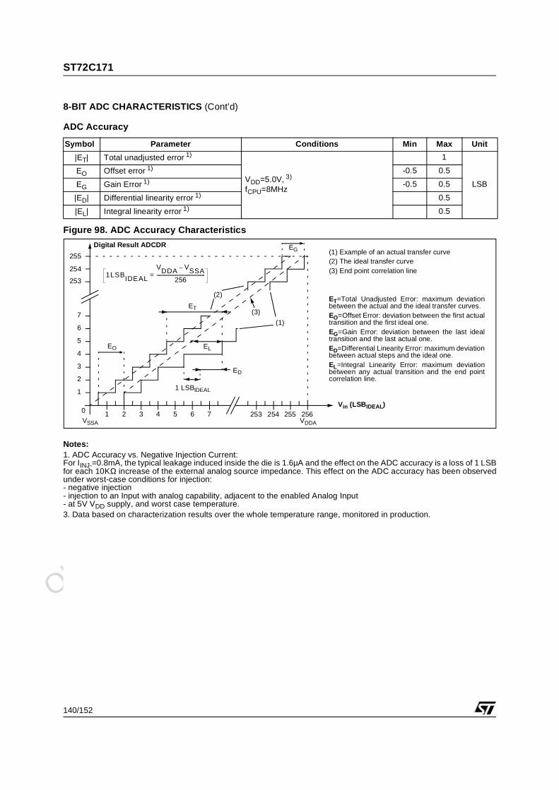
Obsolete Product(
s) - O
bsolete Product(
s)
ST72C171
140/152
8-BIT ADC CHARACTERISTICS (Cont’d)
ADC Accuracy
Figure 98. ADC Accuracy Characteristics
Notes:1. ADC Accuracy vs. Negative Injection Current:For IINJ-=0.8mA, the typical leakage induced inside the die is 1.6µA and the effect on the ADC accuracy is a loss of 1 LSBfor each 10KΩ increase of the external analog source impedance. This effect on the ADC accuracy has been observedunder worst-case conditions for injection:- negative injection- injection to an Input with analog capability, adjacent to the enabled Analog Input- at 5V VDD supply, and worst case temperature.3. Data based on characterization results over the whole temperature range, monitored in production.
Symbol Parameter Conditions Min Max Unit
|ET| Total unadjusted error 1)
VDD=5.0V, 3)
fCPU=8MHz
1
LSB
EO Offset error 1) -0.5 0.5
EG Gain Error 1) -0.5 0.5
|ED| Differential linearity error 1) 0.5
|EL| Integral linearity error 1) 0.5
EO
EG
1 LSBIDEAL
1LSBIDEAL
VDDA VSSA–
256-----------------------------------------=
Vin (LSBIDEAL)
(1) Example of an actual transfer curve(2) The ideal transfer curve(3) End point correlation line
ET=Total Unadjusted Error: maximum deviationbetween the actual and the ideal transfer curves.EO=Offset Error: deviation between the first actualtransition and the first ideal one.EG=Gain Error: deviation between the last idealtransition and the last actual one.ED=Differential Linearity Error: maximum deviationbetween actual steps and the ideal one.EL=Integral Linearity Error: maximum deviationbetween any actual transition and the end pointcorrelation line.
Digital Result ADCDR
255
254
253
5
4
3
2
1
0
7
6
1 2 3 4 5 6 7 253 254 255 256
(1)
(2)
ET
ED
EL
(3)
VDDAVSSA
Obsolete Product(
s) - O
bsolete Product(
s)
ST72C171
141/152
9.13 OP-AMP Module Characteristics
These op-amp specific values take precedence over any generic values given elsewhere in the docu-ment.
(T =25oC, VDD - VSS = 5 V ).
1) AVCL = Closed loop gain (repeater configuration)
2) Tested with positve input connected to internal band gap (reference voltage enabled) and negative in-put floating.
3) Data based on characterization, not tested in production
4) Data guaranteed by design, not tested in production
5) Slew rate is the rate of change from 10% to 90% of the output voltage step.
SPGA1 / SPGA2 - Software Programmable Gain Operational Amplifiers
Symbol Parameter Condition Min Typ Max Unit
|Vio| Input Offset Voltage 3 10 mV
ICC Supply Current per amplifier 2) VDD=5.0V, AVCL=1, no load1) 0.8 2 mA
CMR 3) Common Mode Rejection Ratio 70 dB
SVR 3) Supply Voltage Rejection Ratio 70 dB
Avd 3) Voltage Gain (RL=1KΩ) 100 V/mV
VOH High Level Ouput Voltage (RL=10KΩ) VDD=5V 4.9 V
VOL Low Level Ouput Voltage (RL=10KΩ) VDD=5V 0.10 V
ISC 3)Short circuit Current Sourced
Short circuit Current Sunk
Vo= 5V connected to VSS
Vo= 0V connected to VDD
45
70
mA
mA
GPB Gain Bandwidth Product 4 MHz
SR+ Slew Rate 5) AVCL=11) 1 V/µs
SR- Slew Rate 5) AVCL=11) 1 V/µs
en 3) Thermal Noise 50
Φm 3) Phase margin 40 55 Degrees
Cin 4) Input Capacitance 10 pF
Vicm 4) Common Mode Input Voltage
RangeVSS-0.2
VDD+0.2
V
∆VRefReference Voltage (VDDA/8 step) Precision
±10 %
∆VBG Band Gap Precision ±10 %
∆Gain Programmable Gain Precision ±10 %
nV Hz 1–
Obsolete Product(
s) - O
bsolete Product(
s)
ST72C171
142/152
OP-AMP MODULE CHARACTERISTICS (Cont’d)
1) AVCL = Closed loop gain (repeater configuration)
2) Data based on characterization, not tested in production
3) Data guaranteed by design, not tested in production
4) Slew rate is the rate of change from 10% to 90% of the output voltage step.
OA3 Operational Amplifier
Symbol Parameter Condition Min Typ Max Unit
|Vio| Input Offset Voltage 3 10 mV
ICC Supply Current per amplifier VDD=5.0V, AVCL=1, no load1) 300 500 µA
CMR 2) Common Mode Rejection Ratio 70 dB
SVR 2) Supply Voltage Rejection Ratio 70 dB
Avd 2) Voltage Gain (RL=1KΩ) 100 V/mV
VOH High Level Ouput Voltage (RL=10KΩ) VDDA=5V 4.9 V
VOL Low Level Ouput Voltage (RL=10KΩ) VDDA=5V 0.10 V
ISC 2) Short circuit Current Sourced
Short circuit Current Sunk
Vo= 1 connected to VSS
Vo= 0 connected to VDD
45
70
mA
mA
GPB Gain Bandwidth Product 6 MHz
SR+ Slew Rate4) AVCL=11) 1 V/µs
SR- Slew Rate4) AVCL=11) 1 V/µs
en 2) Thermal Noise 50
Φm 2) Phase margin 40 55 Degrees
Cin 3) Input Capacitance 10 pF
Vicm 3) Common Mode Input Voltage
RangeVSS-0.2
VDD+0.2
V
nV Hz 1–
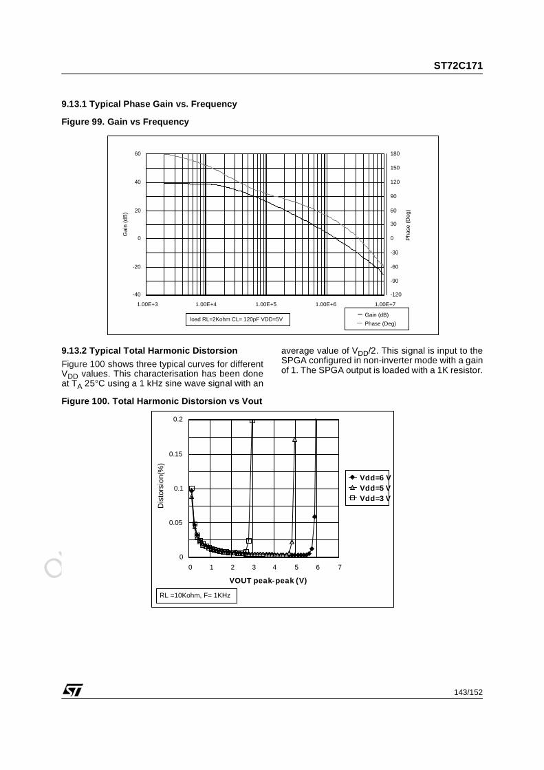
Obsolete Product(
s) - O
bsolete Product(
s)
ST72C171
143/152
9.13.1 Typical Phase Gain vs. Frequency
Figure 99. Gain vs Frequency
9.13.2 Typical Total Harmonic Distorsion
Figure 100 shows three typical curves for differentVDD values. This characterisation has been doneat TA 25°C using a 1 kHz sine wave signal with an
average value of VDD/2. This signal is input to theSPGA configured in non-inverter mode with a gainof 1. The SPGA output is loaded with a 1K resistor.
Figure 100. Total Harmonic Distorsion vs Vout
1.00E+3 1.00E+4 1.00E+5 1.00E+6 1.00E+7
-40
-20
0
20
40
60
Gai
n (d
B)
-120
-90
-60
-30
0
30
60
90
120
150
180
Pha
se (
Deg
)
Gain (dB)
Phase (Deg)load RL=2Kohm CL= 120pF VDD=5V
0 1 2 3 4 5 6 7
VOUT peak-peak (V)
0
0.05
0.1
0.15
0.2
Dis
tors
ion(
%)
Vdd=6V
Vdd=5V
Vdd=3V
RL =10Kohm, F= 1KHz
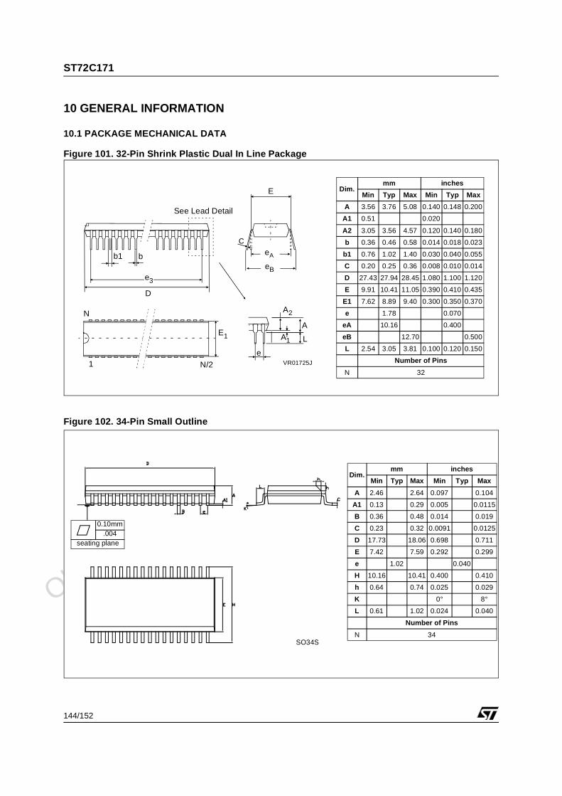
Obsolete Product(
s) - O
bsolete Product(
s)
ST72C171
144/152
10 GENERAL INFORMATION
10.1 PACKAGE MECHANICAL DATA
Figure 101. 32-Pin Shrink Plastic Dual In Line Package
Figure 102. 34-Pin Small Outline
Dim.mm inches
Min Typ Max Min Typ Max
A 3.56 3.76 5.08 0.140 0.148 0.200
A1 0.51 0.020
A2 3.05 3.56 4.57 0.120 0.140 0.180
b 0.36 0.46 0.58 0.014 0.018 0.023
b1 0.76 1.02 1.40 0.030 0.040 0.055
C 0.20 0.25 0.36 0.008 0.010 0.014
D 27.43 27.94 28.45 1.080 1.100 1.120
E 9.91 10.41 11.05 0.390 0.410 0.435
E1 7.62 8.89 9.40 0.300 0.350 0.370
e 1.78 0.070
eA 10.16 0.400
eB 12.70 0.500
L 2.54 3.05 3.81 0.100 0.120 0.150
Number of Pins
N 321
N
b
D
VR01725JN/2
b1
e
A
L
See Lead Detail
E1
e3
A2
A1
E
C
eB
eA
Dim.mm inches
Min Typ Max Min Typ Max
A 2.46 2.64 0.097 0.104
A1 0.13 0.29 0.005 0.0115
B 0.36 0.48 0.014 0.019
C 0.23 0.32 0.0091 0.0125
D 17.73 18.06 0.698 0.711
E 7.42 7.59 0.292 0.299
e 1.02 0.040
H 10.16 10.41 0.400 0.410
h 0.64 0.74 0.025 0.029
K 0° 8°
L 0.61 1.02 0.024 0.040
Number of Pins
N 34SO34S
0.10mm.004
seating plane
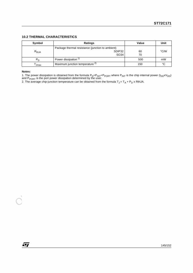
Obsolete Product(
s) - O
bsolete Product(
s)
ST72C171
145/152
10.2 THERMAL CHARACTERISTICS
Notes:1. The power dissipation is obtained from the formula PD=PINT+PPORT where PINT is the chip internal power (IDDxVDD)and PPORT is the port power dissipation determined by the user.2. The average chip-junction temperature can be obtained from the formula TJ = TA + PD x RthJA.
Symbol Ratings Value Unit
RthJA
Package thermal resistance (junction to ambient)SDIP32
SO346070
°C/W
PD Power dissipation 1) 500 mW
TJmax Maximum junction temperature 2) 150 °C
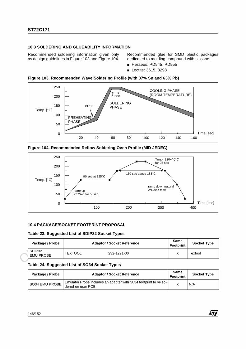
Obsolete Product(
s) - O
bsolete Product(
s)
ST72C171
146/152
10.3 SOLDERING AND GLUEABILITY INFORMATION
Recommended soldering information given onlyas design guidelines in Figure 103 and Figure 104.
Recommended glue for SMD plastic packagesdedicated to molding compound with silicone: Heraeus: PD945, PD955 Loctite: 3615, 3298
Figure 103. Recommended Wave Soldering Profile (with 37% Sn and 63% Pb)
Figure 104. Recommended Reflow Soldering Oven Profile (MID JEDEC)
10.4 PACKAGE/SOCKET FOOTPRINT PROPOSAL
Table 23. Suggested List of SDIP32 Socket Types
Table 24. Suggested List of SO34 Socket Types
Package / Probe Adaptor / Socket ReferenceSame
FootprintSocket Type
SDIP32EMU PROBE
TEXTOOL 232-1291-00 X Textool
Package / Probe Adaptor / Socket ReferenceSame
FootprintSocket Type
SO34 EMU PROBEEmulator Probe includes an adapter with S034 footprint to be sol-dered on user PCB
X N/A
250
200
150
100
50
040 80 120 160
Time [sec]
Temp. [°C]
20 60 100 140
5 sec
COOLING PHASE(ROOM TEMPERATURE)
PREHEATING
80°C
PHASE
SOLDERINGPHASE
250
200
150
100
50
0100 200 300 400
Time [sec]
Temp. [°C]
ramp up2°C/sec for 50sec
90 sec at 125°C150 sec above 183°C
ramp down natural2°C/sec max
Tmax=220+/-5°Cfor 25 sec
Obsolete Product(
s) - O
bsolete Product(
s)
ST72C171
147/152
11 DEVICE CONFIGURATION AND ORDERING INFORMATIONThe device is available for production a user pro-grammable version (FLASH). FLASH devices areshipped to customers with a default content (FFh).FLASH devices have to be configured by the cus-tomer using the Option Bytes.
11.1 OPTION BYTES
The two option bytes allow the hardware configu-ration of the microcontroller to be selected.The option bytes have no address in the memorymap and can be accessed only in programmingmode (for example using a standard ST7 program-ming tool). The default content of the FLASH isfixed to FFh.In masked ROM devices, the option bytes arefixed in hardware by the ROM code (see optionlist).
USER OPTION BYTE 0
Bit 7:1 = Reserved, must always be 1.
Bit 1= OA3E Op-Amp 3 EnableThis option bit enables or disables the third Op-Amp of the on-chip Op-Amp Module.0: OE3 disabled1: OE3 enabled
Bit 0 = FMP Full memory protection.This option bit enables or disables external accessto the internal program memory (read-out protec-tion). Clearing this bit causes the erasing (to 00h)of the whole memory (including the option byte).0: Program memory not read-out protected1: Program memory read-out protected
USER OPTION BYTE 1
Bit 7 = CFC Clock filter control on/offThis option bit enables or disables the clock filter(CF) features.
0: Clock filter enabled1: Clock filter disabled
Bit 6:4 = OSC[2:0] Oscillator selectionThese three option bits can be used to select themain oscillator as shown in Table 25.
Bit 3:2 = LVD[1:0] Low voltage detection selectionThese option bits enable the LVD block with a se-lected threshold as shown in Table 26.
Bit 1 = WDG HALT Watchdog and halt modeThis option bit determines if a RESET is generatedwhen entering HALT mode while the Watchdog isactive.0: No Reset generation when entering Halt mode1: Reset generation when entering Halt mode
Bit 0 = WDG SW Hardware or software watchdog This option bit selects the watchdog type.0: Hardware (watchdog always enabled)1: Software (watchdog to be enabled by software)Table 25. Main Oscillator Configuration
Table 26. LVD Threshold Configuration
Selected Oscillator OSC2 OSC1 OSC0
External Clock (Stand-by) 1 1 1
~4 MHz Internal RC 1 1 0
1~14 MHz External RC 1 0 X
Low Power Resonator (LP) 0 1 1
Medium Power Resonator (MP) 0 1 0
Medium Speed Resonator (MS) 0 0 1
High Speed Resonator (HS) 0 0 0
Configuration LVD1 LVD0
LVD Off 1 1
Highest Voltage Threshold (∼4.50V) 1 0
Medium Voltage Threshold (∼4.05V) 0 1
Lowest Voltage Threshold (∼3.45V) 0 0
USER OPTION BYTE 07 0
USER OPTION BYTE 17 0
Reserved OA3E FMP CFCOSC
2OSC
1OSC
0LVD1 LVD0
WDGHALT
WDGSW
DefaultValue
1 1 1 1 1 1 1 0 1 1 1 0 1 1 1 1
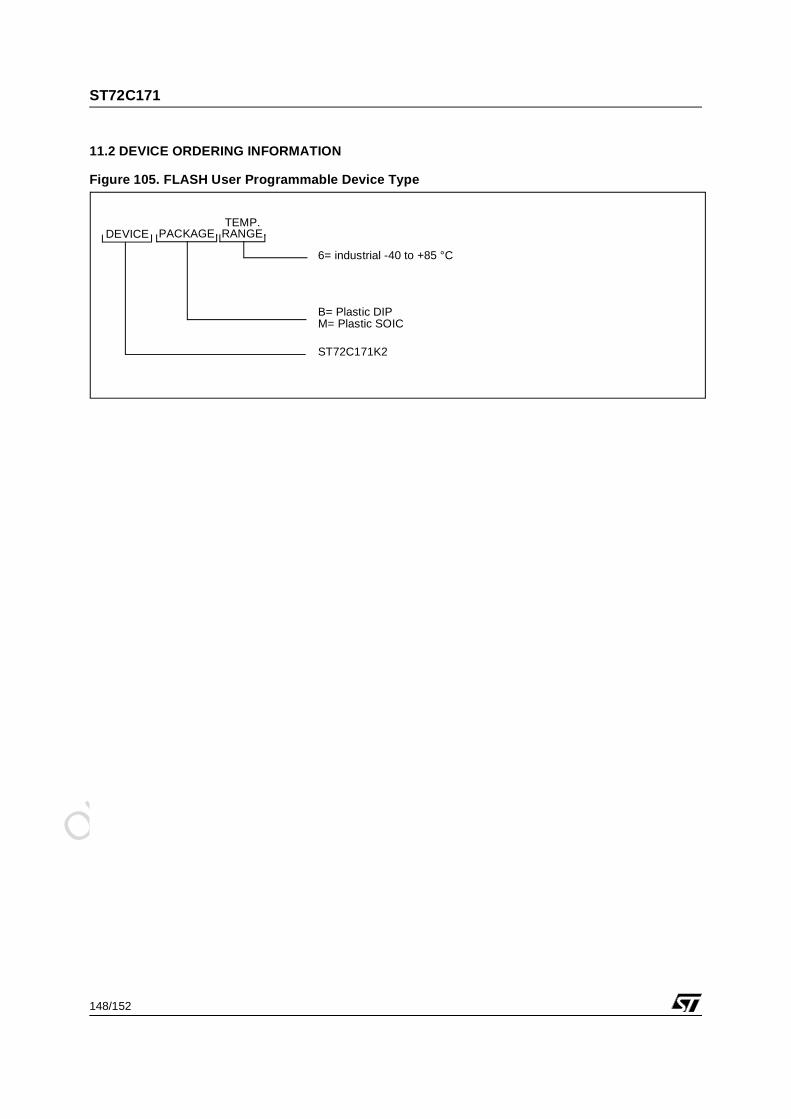
Obsolete Product(
s) - O
bsolete Product(
s)
ST72C171
148/152
11.2 DEVICE ORDERING INFORMATION
Figure 105. FLASH User Programmable Device Type
DEVICE PACKAGETEMP.RANGE
6= industrial -40 to +85 °C
B= Plastic DIPM= Plastic SOIC
ST72C171K2
Obsolete Product(
s) - O
bsolete Product(
s)
ST72C171
149/152
11.3 DEVELOPMENT TOOLS
STmicroelectronics offers a range of hardwareand software development tools for the ST7 micro-controller family. Full details of tools available forthe ST7 from third party manufacturers can be ob-tain from the STMicroelectronics Internet site:http//mcu.st.com.
Third Party Tools ACTUM BP COSMIC CMX DATA I/O HITEX HIWARE ISYSTEM KANDA LEAP
Tools from these manufacturers include C compli-ers, emulators and gang programmers.
STMicroelectronics Tools
Two types of development tool are offered by ST,all of them connect to a PC via a parallel (LPT)port: see Table 27 and Table 28 for more details.
Table 27. STMicroelectronic Tool Features
Table 28. Dedicated STMicroelectronics Development Tools
Note:1. In-Situ Programming (ISP) interface for FLASH devices.
In-Circuit Emulation Programming Capability1) Software Included
ST7 HDS2 EmulatorYes, powerful emulation features including trace/ logic analyzer
NoST7 CD ROM with:
– ST7 Assembly toolchain– STVD7 and WGDB7 powerful
Source Level Debugger for Win 3.1, Win 95 and NT
– C compiler demo versions– ST Realizer for Win 3.1 and Win
95. – Windows Programming Tools
for Win 3.1, Win 95 and NT
ST7 Programming Board NoYes (All packages),support also ISP 1)
Supported Product ST7 HDS2 Emulator ST7 Programming Board
ST72C171K2, ST7MDT6-EMU2B
ST7MDT6-EPB2/EU
ST7MDT6-EPB2/US
ST7MDT6-EPB2/UK
Obsolete Product(
s) - O
bsolete Product(
s)
ST72C171
150/152
11.4 ST7 APPLICATION NOTES
11.5 TO GET MORE INFORMATION
To get the latest information on this product please use the ST web server: http://mcu.st.com/
IDENTIFICATION DESCRIPTIONPROGRAMMING AND TOOLS AN985 EXECUTING CODE IN ST7 RAMAN986 USING THE ST7 INDIRECT ADDRESSING MODEAN987 ST7 IN-CIRCUIT PROGRAMMINGAN988 STARTING WITH ST7 ASSEMBLY TOOL CHAINAN989 STARTING WITH ST7 HIWARE CAN1039 ST7 MATH UTILITY ROUTINESAN1064 WRITING OPTIMIZED HIWARE C LANGUAGE FOR ST7AN1106 TRANSLATING ASSEMBLY CODE FROM HC05 TO ST7EXAMPLE DRIVERS AN969 ST7 SCI COMMUNICATION BETWEEN THE ST7 AND A PCAN970 ST7 SPI COMMUNICATION BETWEEN THE ST7 AND E²PROMAN971 ST7 I²C COMMUNICATION BETWEEN THE ST7 AND E²PROMAN972 ST7 SOFTWARE SPI MASTER COMMUNICATIONAN973 SCI SOFTWARE COMMUNICATION WITH A PC USING ST72251 16-BIT TIMERAN974 REAL TIME CLOCK WITH THE ST7 TIMER OUTPUT COMPAREAN976 DRIVING A BUZZER USING THE ST7 PWM FUNCTIONAN979 DRIVING AN ANALOG KEYBOARD WITH THE ST7 ADCAN980 ST7 KEYPAD DECODING TECHNIQUES, IMPLEMENTING WAKE-UP ON KEYSTROKEAN1017 USING THE ST7 USB MICROCONTROLLERAN1041 USING ST7 PWM SIGNAL TO GENERATE ANALOG OUTPUT (SINUSOID)AN1042 ST7 ROUTINE FOR I²C SLAVE MODE MANAGEMENTAN1044 MULTIPLE INTERRUPT SOURCES MANAGEMENT FOR ST7 MCUSAN1045 ST7 SOFTWARE IMPLEMENTATION OF I²C BUS MASTERAN1046 ST7 UART EMULATION SOFTWAREAN1047 MANAGING RECEPTION ERRORS WITH THE ST7 SCI PERIPHERALAN1048 ST7 SOFTWARE LCD DRIVERAN1078 ST7 TIMER PWM DUTY CYCLE SWITCH FOR TRUE 0% or 100% DUTY CYCLEAN1082 DESCRIPTION OF THE ST72141 MOTOR CONTROLAN1083 ST72141 BLDC MOTOR CONTROL SOFTWARE AND FLOWCHART EXAMPLEAN1129 PERMANENT MAGNET DC MOTOR DRIVE.AN1130 BRUSHLESS DC MOTOR DRIVE WITH ST72141AN1148 USING THE ST7263 FOR DESIGNING A USB MOUSEAN1149 HANDLING SUSPEND MODE ON A USB MOUSEAN1180 USING THE ST7263 KIT TO IMPLEMENT A USB GAME PADAN1182 USING THE ST7 USB LOW-SPEED FIRMWAREPRODUCT OPTIMIZATION AN982 USING CERAMIC RESONATORS WITH THE ST7AN1014 HOW TO MINIMIZE THE ST7 POWER CONSUMPTIONAN1070 ST7 CHECKSUM SELFCHECKING CAPABILITYAN1179 PROGRAMMING ST7 FLASH MICROCONTROLLERS IN REMOTE ISPPRODUCT EVALUATION AN910 ST7 AND ST9 PERFORMANCE BENCHMARKINGAN990 ST7 BENEFITS VERSUS INDUSTRY STANDARDAN1086 ST7 / ST10U435 CAN-do SOLUTIONS FOR CAR MULTIPLEXINGAN1150 BENCHMARK ST72 VS PC16AN1151 PERFORMANCE COMPARISON BETWEEN ST72254 & PC16F8
Obsolete Product(
s) - O
bsolete Product(
s)
ST72C171
151/152
12 SUMMARY OF CHANGESDescription of the changes between the current release of the specification and the previous one.
Revision Main changes Date
1.4 Added Figure 99 and Figure 100. Oct-00
Obsolete Product(
s) - O
bsolete Product(
s)
ST72C171
152/152
Notes:
Information furnished is believed to be accurate and reliable. However, STMicroelectronics assumes no responsibility for the consequencesof use of such information nor for any infringement of patents or other rights of third parties which may result from its use. No license is grantedby implication or otherwise under any patent or patent rights of STMicroelectronics. Specifications mentioned in this publication are subjectto change without notice. This publication supersedes and replaces all information previously supplied. STMicroelectronics products are notauthorized for use as critical components in life support devices or systems without the express written approval of STMicroelectronics.
The ST logo is a registered trademark of STMicroelectronics
2000 STMicroelectronics - All Rights Reserved.
Purchase of I2C Components by STMicroelectronics conveys a license under the Philips I2C Patent. Rights to use these components in an I2C system is granted provided that the system conforms to the I2C Standard Specification as defined by Philips.
STMicroelectronics Group of CompaniesAustralia - Brazil - China - Finland - France - Germany - Hong Kong - India - Italy - Japan - Malaysia - Malta - Morocco - Singapore - Spain
Sweden - Switzerland - United Kingdom - U.S.A.
http://www.st.com