Embed Size (px)
Citation preview
December 2010 Doc ID 15931 Rev 2 1/18
18
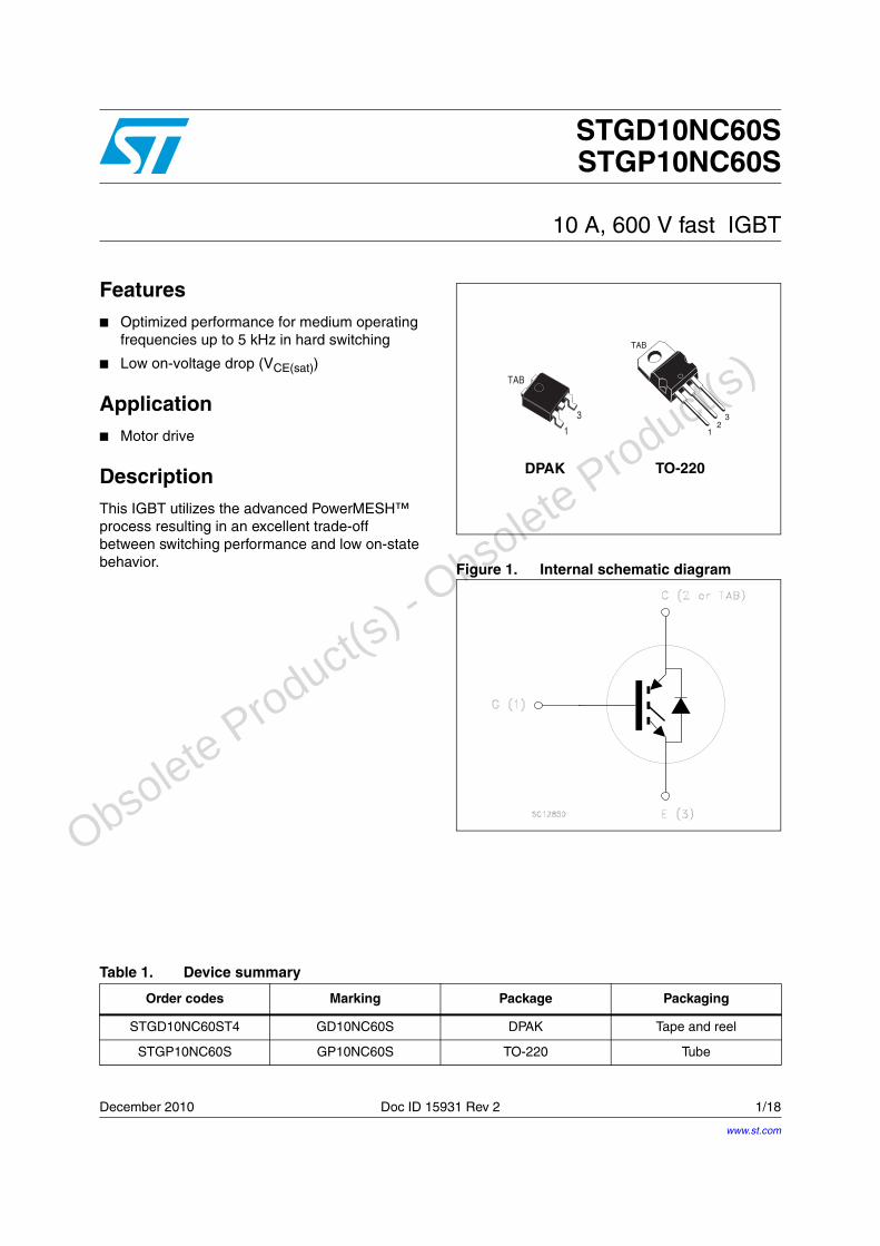
STGD10NC60SSTGP10NC60S
10 A, 600 V fast IGBT
Features■ Optimized performance for medium operating
frequencies up to 5 kHz in hard switching
■ Low on-voltage drop (VCE(sat))
Application■ Motor drive
DescriptionThis IGBT utilizes the advanced PowerMESH™ process resulting in an excellent trade-off between switching performance and low on-state behavior.
Figure 1. Internal schematic diagram
DPAK
1
3
TAB
12
3
TAB
TO-220
Table 1. Device summary
Order codes Marking Package Packaging
STGD10NC60ST4 GD10NC60S DPAK Tape and reel
STGP10NC60S GP10NC60S TO-220 Tube
www.st.com
O
bsolete Product(
s) - O
bsolete Product(
s)
Contents STGD10NC60S, STGP10NC60S
Contents
1 Electrical ratings . . . . . . . . . . . . . . . . . . . . . . . . . . . . . . . . . . . . . . . . . . . . 3
2 Electrical characteristics . . . . . . . . . . . . . . . . . . . . . . . . . . . . . . . . . . . . . 4
2.1 Electrical characteristics (curves) . . . . . . . . . . . . . . . . . . . . . . . . . . . . . . . . 5
3 Test circuits . . . . . . . . . . . . . . . . . . . . . . . . . . . . . . . . . . . . . . . . . . . . . . . 8
4 Package mechanical data . . . . . . . . . . . . . . . . . . . . . . . . . . . . . . . . . . . . . 9
5 Packaging mechanical data . . . . . . . . . . . . . . . . . . . . . . . . . . . . . . . . . . 14
6 Revision history . . . . . . . . . . . . . . . . . . . . . . . . . . . . . . . . . . . . . . . . . . . 17
O
bsolete Product(
s) - O
bsolete Product(
s)
STGD10NC60S, STGP10NC60S Electrical ratings
Doc ID 15931 Rev 2 3/18
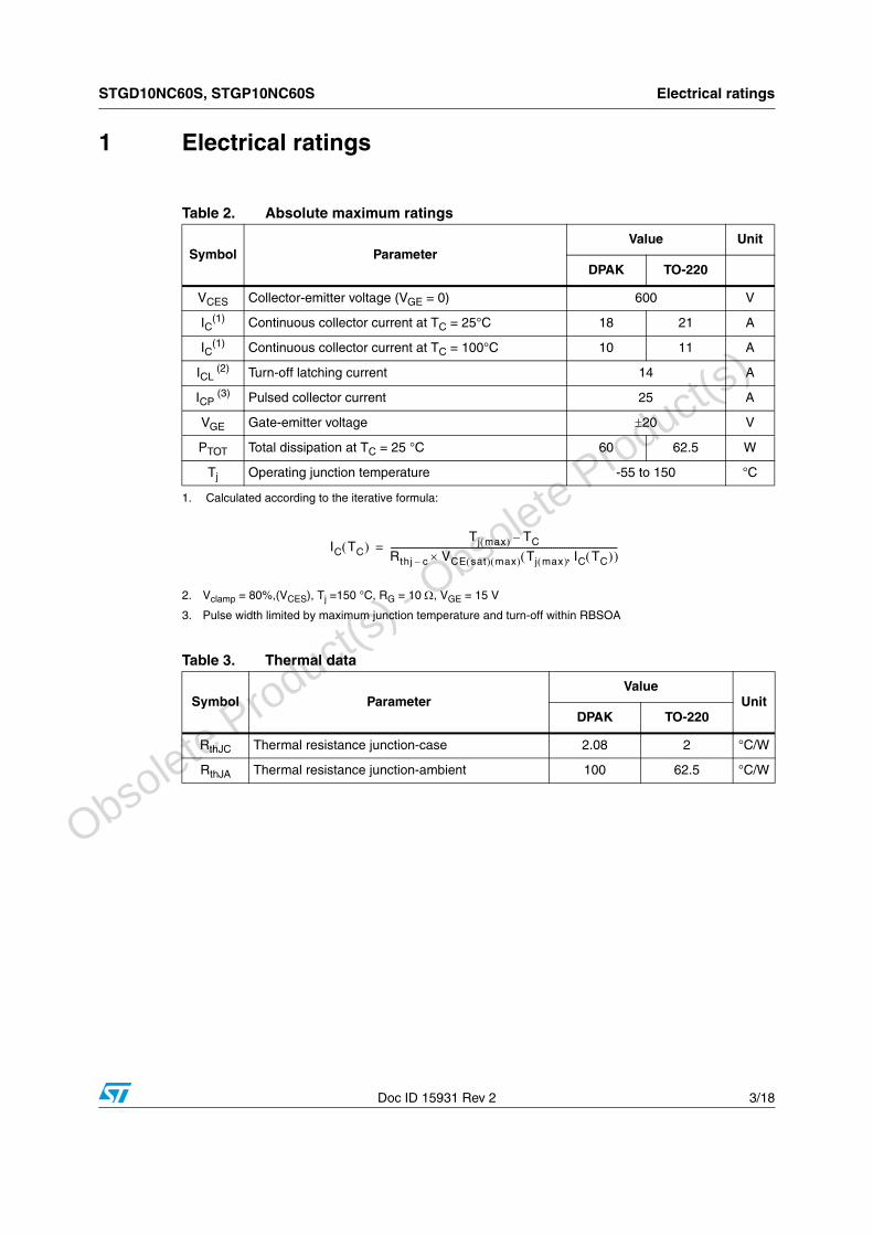
1 Electrical ratings
Table 2. Absolute maximum ratings
Symbol ParameterValue Unit
DPAK TO-220
VCES Collector-emitter voltage (VGE = 0) 600 V
IC(1)
1. Calculated according to the iterative formula:
Continuous collector current at TC = 25°C 18 21 A
IC(1) Continuous collector current at TC = 100°C 10 11 A
ICL (2)
2. Vclamp = 80%,(VCES), Tj =150 °C, RG = 10 Ω, VGE = 15 V
Turn-off latching current 14 A
ICP (3)
3. Pulse width limited by maximum junction temperature and turn-off within RBSOA
Pulsed collector current 25 A
VGE Gate-emitter voltage ±20 V
PTOT Total dissipation at TC = 25 °C 60 62.5 W
Tj Operating junction temperature -55 to 150 °C
Table 3. Thermal data
Symbol ParameterValue
UnitDPAK TO-220
RthJC Thermal resistance junction-case 2.08 2 °C/W
RthJA Thermal resistance junction-ambient 100 62.5 °C/W
IC TC( )Tj max( ) TC–
Rthj c– VCE sat( ) max( ) Tj max( ) IC TC( ),( )×-------------------------------------------------------------------------------------------------------=
O
bsolete Product(
s) - O
bsolete Product(
s)
Electrical characteristics STGD10NC60S, STGP10NC60S
4/18 Doc ID 15931 Rev 2
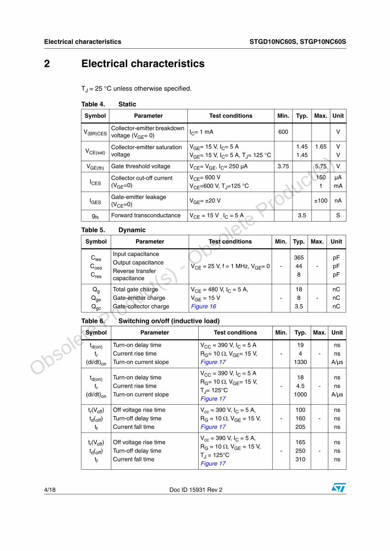
2 Electrical characteristics
TJ = 25 °C unless otherwise specified.
Table 4. Static
Symbol Parameter Test conditions Min. Typ. Max. Unit
V(BR)CESCollector-emitter breakdown voltage (VGE= 0)
IC= 1 mA 600 V
VCE(sat)Collector-emitter saturation voltage
VGE= 15 V, IC= 5 A VGE= 15 V, IC= 5 A, TJ= 125 °C
1.451.45
1.65 VV
VGE(th) Gate threshold voltage VCE= VGE, IC= 250 µA 3.75 5.75 V
ICESCollector cut-off current (VGE=0)
VCE= 600 V
VCE=600 V, TJ=125 °C
150
1
µA
mA
IGESGate-emitter leakage (VCE=0)
VGE= ±20 V ±100 nA
gfs Forward transconductance VCE = 15 V , IC = 5 A 3.5 S
Table 5. Dynamic
Symbol Parameter Test conditions Min. Typ. Max. Unit
Cies
Coes
Cres
Input capacitance
Output capacitance
Reverse transfer capacitance
VCE = 25 V, f = 1 MHz, VGE= 0 -
365
448
-
pF
pFpF
Qg
Qge
Qgc
Total gate charge
Gate-emitter charge
Gate-collector charge
VCE = 480 V, IC = 5 A,
VGE = 15 V
Figure 16
-
18
8
3.5
-
nC
nC
nC
Table 6. Switching on/off (inductive load)
Symbol Parameter Test conditions Min. Typ. Max. Unit
td(on)
tr(di/dt)on
Turn-on delay time
Current rise timeTurn-on current slope
VCC = 390 V, IC = 5 A
RG= 10 Ω, VGE= 15 V,Figure 17
-
19
41330
-
ns
nsA/µs
td(on)
tr(di/dt)on
Turn-on delay time
Current rise timeTurn-on current slope
VCC = 390 V, IC = 5 A RG= 10 Ω, VGE= 15 V,
TJ= 125°C
Figure 17
-
18
4.51000
-
ns
nsA/µs
tr(Voff)
td(off)tf
Off voltage rise time
Turn-off delay timeCurrent fall time
Vcc = 390 V, IC = 5 A,
RG = 10 Ω, VGE = 15 V,Figure 17
-
100
160205
-
ns
nsns
tr(Voff)
td(off)tf
Off voltage rise time
Turn-off delay timeCurrent fall time
Vcc = 390 V, IC = 5 A, RG = 10 Ω, VGE = 15 V,
TJ = 125°C
Figure 17
-
165
250310
-
ns
nsns
O
bsolete Product(
s) - O
bsolete Product(
s)
STGD10NC60S, STGP10NC60S Electrical characteristics
Doc ID 15931 Rev 2 5/18
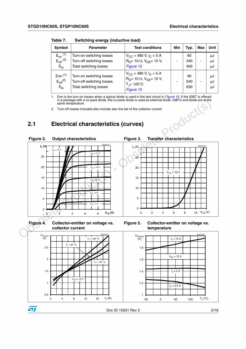
2.1 Electrical characteristics (curves)
Table 7. Switching energy (inductive load)
Symbol Parameter Test conditions Min Typ. Max Unit
Eon (1)
Eoff (2)
Ets
1. Eon is the turn-on losses when a typical diode is used in the test circuit in Figure 15. If the IGBT is offered in a package with a co-pack diode, the co-pack diode is used as external diode. IGBTs and diode are at the same temperature
2. Turn-off losses included also include also the tail of the collector current
Turn-on switching lossesTurn-off switching losses
Total switching losses
VCC = 480 V, IC = 5 A RG= 10 Ω, VGE= 15 V,
Figure 15
-60340
400
-µJµJ
µJ
Eon (1)
Eoff(2)
Ets
Turn-on switching lossesTurn-off switching losses
Total switching losses
VCC = 480 V, IC = 5 A
RG= 10 Ω, VGE= 15 V,
TJ= 125°C Figure 15
-90540
630
-µJµJ
µJ
Figure 2. Output characteristics Figure 3. Transfer characteristics
Figure 4. Collector-emitter on voltage vs. collector current
Figure 5. Collector-emitter on voltage vs. temperature
0
5
10
15
20
25
30
0 2 4 6 8 10
IC (A)
VCE (V)
VGE = 7 V
VGE = 8 V
VGE = 9 V
VGE = 10 V
VGE = 11 V
VGE = 15 V
AM07871v1AM07872v1
0
5
10
15
20
25
30
0 2 4 6 8 10 12
IC (A)
VGE (V)
VCE = 10 V
AM07873v1
0.5
1
1.5
2
2.5
3
0 4 8 12 16 20
VCE(sat)(V)
IC (A)
TJ = -50 °C
TJ = 25 °C
TJ = 150 °C
VGE = 15 V
AM07874v1
1
1.2
1.4
1.6
1.8
2
-50 0 50 100 150
VCE(sat)(V)
TJ (°C)
IC = 10 A
IC = 2.5 A
IC = 5 A
VGE = 15 V
O
bsolete Product(
s) - O
bsolete Product(
s)
Electrical characteristics STGD10NC60S, STGP10NC60S
6/18 Doc ID 15931 Rev 2
Figure 6. Normalized breakdown voltage vs. temperature
Figure 7. Normalized gate threshold voltage vs. temperature
Figure 8. Gate charge vs. gate-emitter voltage
Figure 9. Capacitance variations
AM07875v1
0.9
0.95
1
1.05
1.1
1.15
-50 0 50 100 150
VCES(norm)
TJ (°C)
IC = 1 mA
AM07876v1
0.6
0.7
0.8
0.9
1
1.1
1.2
-50 0 50 100 150
VGE(th) (norm)
TJ (°C)
VGE = VCE
IC = 250 µA
AM07877v1
0
4
8
12
16
20
0 4 8 12 16 20
VGE (V)
QG (nC)
VCC = 480 VIC = 5 A
AM07878v1
0
200
400
600
800
0 10 20 30 40 50
C (pF)
VCE (V)
f = 1 MHzVGE = 0
Cies
Coes
Cres
Figure 10. Switching losses vs. temperature Figure 11. Switching losses vs. gate resistance
AM07879v1
0
100
200
300
400
500
600
25 50 75 100 125
E (µJ)
TJ (°C)
VCC = 480 V, VGE= 15 V IC = 5 A, RG =10 Ω
EON
EOFF
AM07880v1
0
100
200
300
400
500
600
0 40 80 120 160 200
E (µJ)
RG (Ω)
VCC = 480 V, VGE = 15 V IC = 5 A, TJ 125 °C
EON
EOFF
O
bsolete Product(
s) - O
bsolete Product(
s)
STGD10NC60S, STGP10NC60S Electrical characteristics
Doc ID 15931 Rev 2 7/18
Figure 12. Switching losses vs. collector current
Figure 13. Turn-off SOA
Figure 14. Thermal impedance for DPAK and TO-220
AM07881v1
0
100
200
300
400
500
600
1 2 3 4 5
E (µJ)
IC (A)
VCC = 480 V, VGE = 15 VRG =10 Ω, TJ 125 °C
EON
EOFF
AM07882v1
0.01
0.1
1
10
100
0.1 1 10 100
IC (A)
VCE (V)
O
bsolete Product(
s) - O
bsolete Product(
s)
Test circuits STGD10NC60S, STGP10NC60S
8/18 Doc ID 15931 Rev 2
3 Test circuits
Figure 15. Test circuit for inductive load switching
Figure 16. Gate charge test circuit
Figure 17. Switching waveforms
O
bsolete Product(
s) - O
bsolete Product(
s)
STGD10NC60S, STGP10NC60S Package mechanical data
Doc ID 15931 Rev 2 9/18
4 Package mechanical data
In order to meet environmental requirements, ST offers these devices in different grades of ECOPACK® packages, depending on their level of environmental compliance. ECOPACK® specifications, grade definitions and product status are available at: www.st.com. ECOPACK is an ST trademark.
O
bsolete Product(
s) - O
bsolete Product(
s)
Package mechanical data STGD10NC60S, STGP10NC60S
10/18 Doc ID 15931 Rev 2
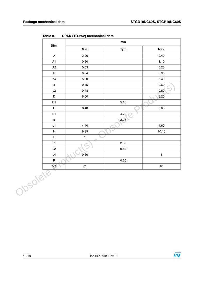
Table 8. DPAK (TO-252) mechanical data
Dim.mm
Min. Typ. Max.
A 2.20 2.40
A1 0.90 1.10
A2 0.03 0.23
b 0.64 0.90
b4 5.20 5.40
c 0.45 0.60
c2 0.48 0.60
D 6.00 6.20
D1 5.10
E 6.40 6.60
E1 4.70
e 2.28
e1 4.40 4.60
H 9.35 10.10
L 1
L1 2.80
L2 0.80
L4 0.60 1
R 0.20
V2 0° 8°
O
bsolete Product(
s) - O
bsolete Product(
s)
STGD10NC60S, STGP10NC60S Package mechanical data
Doc ID 15931 Rev 2 11/18
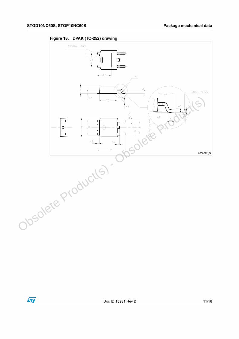
Figure 18. DPAK (TO-252) drawing
0068772_G
O
bsolete Product(
s) - O
bsolete Product(
s)
Package mechanical data STGD10NC60S, STGP10NC60S
12/18 Doc ID 15931 Rev 2
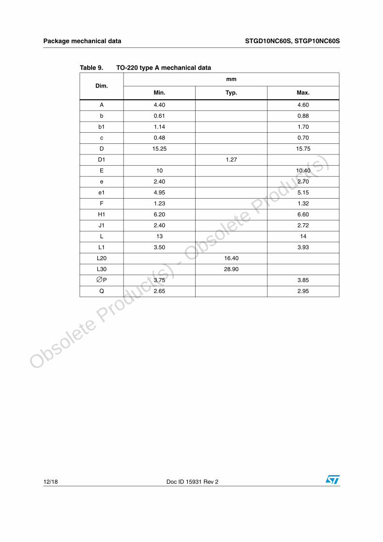
Table 9. TO-220 type A mechanical data
Dim.mm
Min. Typ. Max.
A 4.40 4.60
b 0.61 0.88
b1 1.14 1.70
c 0.48 0.70
D 15.25 15.75
D1 1.27
E 10 10.40
e 2.40 2.70
e1 4.95 5.15
F 1.23 1.32
H1 6.20 6.60
J1 2.40 2.72
L 13 14
L1 3.50 3.93
L20 16.40
L30 28.90
∅P 3.75 3.85
Q 2.65 2.95
O
bsolete Product(
s) - O
bsolete Product(
s)
STGD10NC60S, STGP10NC60S Package mechanical data
Doc ID 15931 Rev 2 13/18
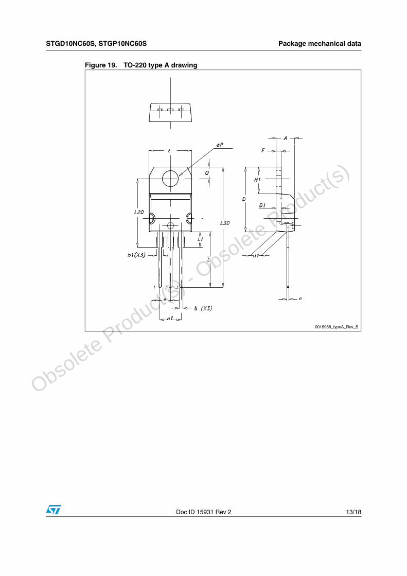
Figure 19. TO-220 type A drawing
0015988_typeA_Rev_S
O
bsolete Product(
s) - O
bsolete Product(
s)
Packaging mechanical data STGD10NC60S, STGP10NC60S
14/18 Doc ID 15931 Rev 2
5 Packaging mechanical data
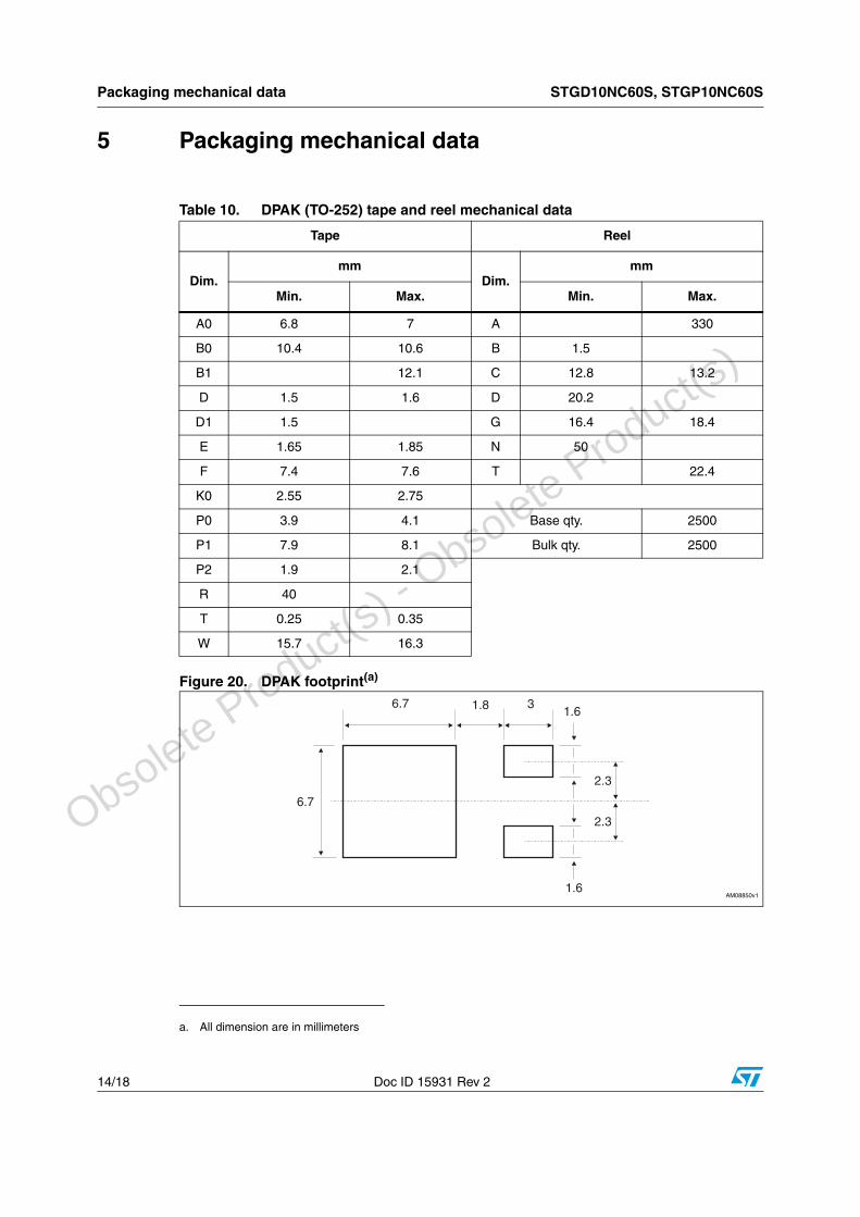
Figure 20. DPAK footprint(a)
Table 10. DPAK (TO-252) tape and reel mechanical data
Tape Reel
Dim.mm
Dim.mm
Min. Max. Min. Max.
A0 6.8 7 A 330
B0 10.4 10.6 B 1.5
B1 12.1 C 12.8 13.2
D 1.5 1.6 D 20.2
D1 1.5 G 16.4 18.4
E 1.65 1.85 N 50
F 7.4 7.6 T 22.4
K0 2.55 2.75
P0 3.9 4.1 Base qty. 2500
P1 7.9 8.1 Bulk qty. 2500
P2 1.9 2.1
R 40
T 0.25 0.35
W 15.7 16.3
a. All dimension are in millimeters
6.7
1.6
1.6
2.3
2.3
6.7 1.8 3
AM08850v1
O
bsolete Product(
s) - O
bsolete Product(
s)
STGD10NC60S, STGP10NC60S Packaging mechanical data
Doc ID 15931 Rev 2 15/18
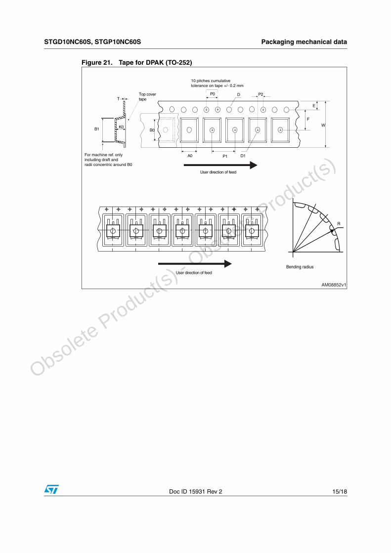
Figure 21. Tape for DPAK (TO-252)
P1A0 D1
P0
F
W
E
D
B0K0
T
User direction of feed
P2
10 pitches cumulativetolerance on tape +/- 0.2 mm
User direction of feed
R
Bending radius
B1
For machine ref. onlyincluding draft andradii concentric around B0
AM08852v1
Top covertape
O
bsolete Product(
s) - O
bsolete Product(
s)
Packaging mechanical data STGD10NC60S, STGP10NC60S
16/18 Doc ID 15931 Rev 2
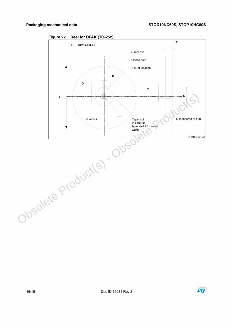
Figure 22. Reel for DPAK (TO-252)
A
D
B
Full radius G measured at hub
C
N
REEL DIMENSIONS
40mm min.
Access hole
At sl ot location
T
Tape slot in core fortape start 25 mm min.width
AM08851v2
O
bsolete Product(
s) - O
bsolete Product(
s)
STGD10NC60S, STGP10NC60S Revision history
Doc ID 15931 Rev 2 17/18
6 Revision history
Table 11. Document revision history
Date Revision Changes
06-Jul-2009 1 Initial release
17-Dec-2010 2Inserted Section 2.1: Electrical characteristics (curves) on page 5
O
bsolete Product(
s) - O
bsolete Product(
s)
STGD10NC60S, STGP10NC60S
18/18 Doc ID 15931 Rev 2
Please Read Carefully:
Information in this document is provided solely in connection with ST products. STMicroelectronics NV and its subsidiaries (“ST”) reserve theright to make changes, corrections, modifications or improvements, to this document, and the products and services described herein at anytime, without notice.
All ST products are sold pursuant to ST’s terms and conditions of sale.
Purchasers are solely responsible for the choice, selection and use of the ST products and services described herein, and ST assumes noliability whatsoever relating to the choice, selection or use of the ST products and services described herein.
No license, express or implied, by estoppel or otherwise, to any intellectual property rights is granted under this document. If any part of thisdocument refers to any third party products or services it shall not be deemed a license grant by ST for the use of such third party productsor services, or any intellectual property contained therein or considered as a warranty covering the use in any manner whatsoever of suchthird party products or services or any intellectual property contained therein.
UNLESS OTHERWISE SET FORTH IN ST’S TERMS AND CONDITIONS OF SALE ST DISCLAIMS ANY EXPRESS OR IMPLIEDWARRANTY WITH RESPECT TO THE USE AND/OR SALE OF ST PRODUCTS INCLUDING WITHOUT LIMITATION IMPLIEDWARRANTIES OF MERCHANTABILITY, FITNESS FOR A PARTICULAR PURPOSE (AND THEIR EQUIVALENTS UNDER THE LAWSOF ANY JURISDICTION), OR INFRINGEMENT OF ANY PATENT, COPYRIGHT OR OTHER INTELLECTUAL PROPERTY RIGHT.
UNLESS EXPRESSLY APPROVED IN WRITING BY AN AUTHORIZED ST REPRESENTATIVE, ST PRODUCTS ARE NOTRECOMMENDED, AUTHORIZED OR WARRANTED FOR USE IN MILITARY, AIR CRAFT, SPACE, LIFE SAVING, OR LIFE SUSTAININGAPPLICATIONS, NOR IN PRODUCTS OR SYSTEMS WHERE FAILURE OR MALFUNCTION MAY RESULT IN PERSONAL INJURY,DEATH, OR SEVERE PROPERTY OR ENVIRONMENTAL DAMAGE. ST PRODUCTS WHICH ARE NOT SPECIFIED AS "AUTOMOTIVEGRADE" MAY ONLY BE USED IN AUTOMOTIVE APPLICATIONS AT USER’S OWN RISK.
Resale of ST products with provisions different from the statements and/or technical features set forth in this document shall immediately voidany warranty granted by ST for the ST product or service described herein and shall not create or extend in any manner whatsoever, anyliability of ST.
ST and the ST logo are trademarks or registered trademarks of ST in various countries.
Information in this document supersedes and replaces all information previously supplied.
The ST logo is a registered trademark of STMicroelectronics. All other names are the property of their respective owners.
© 2010 STMicroelectronics - All rights reserved
STMicroelectronics group of companies
Australia - Belgium - Brazil - Canada - China - Czech Republic - Finland - France - Germany - Hong Kong - India - Israel - Italy - Japan - Malaysia - Malta - Morocco - Philippines - Singapore - Spain - Sweden - Switzerland - United Kingdom - United States of America
www.st.com
O
bsolete Product(
s) - O
bsolete Product(
s)