Embed Size (px)
Citation preview
1/28
L6611
April 2002
OV/UV DETECTION FOR 3.3V, +5V, ±12V RAILS AND 5V (OR 3.3V) AUX. VOLTAGE
AC MAINS UV (BROWNOUT) DETECTION WITH HYSTERESIS
ON-LINE DIGITAL TRIMMING FOR 5V/12V, 3.3V, 5V (OR 3.3V) AUX. FEEDBACK REFERENCES AND AC MAINS UV.
DIGITALLY SELECTABLE OPTIONS ERROR AMPLIFIERS FOR 5V/12V RAILS
(MAIN SUPPLY), 3V3 POST-REGULATOR (MAG_AMP OR LINEAR) AND AUXILIARY SUPPLY.
MAIN SUPPLY ON/OFF CONTROL AND POWER GOOD SIGNAL
50mA CROWBAR DRIVE FOR AUXILIARY OUTPUT OVP.
OPEN GROUND PROTECTION 8ms DIGITAL SOFT START 64 ms UV/OC BLANKING AT START-UP
APPLICATIONS SWITCHING POWER SUPPLIES FOR
DESKTOP PC'S, SERVERS AND WEB SERVERS
SUPERVISOR FOR DISTRIBUTED POWER
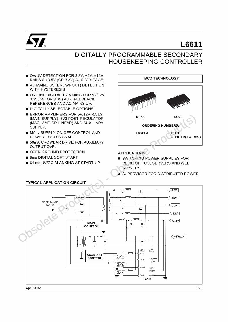
DIP20 SO20
ORDERING NUMBERS:
L6611N L6611DL6611DTR(T & Reel)
DIGITALLY PROGRAMMABLE SECONDARYHOUSEKEEPING CONTROLLER
TYPICAL APPLICATION CIRCUIT
+5Vaux
WIDE RANGEMAINS
+5V
COM
+3.3V
+12V
-
+
MAIN CONTROL
AUXILIARYCONTROL
VDD
12VCout
Gnd
MFault
Aout
5V
3V3
L6611
-12V
-12V
DmonBout
BCD TECHNOLOGY
Obsolete Product(
s) - O
bsolete Product(
s)
Obsolete Product(
s) - O
bsolete Product(
s)
Obsolete Product(s) - Obsolete Product(s) - O
bsolet
Obsolete Product(s) - Obsolete Product(s) - O
bsolet
L6611
2/28
BLO
CK
DIA
GR
AM
+3V3
+12V
Vdd
OV
Logic and Programmable Trimming
Prog
Cinv
Cout
Dm
on
Vdd
2.50V(B
)
uvov
OC
P B
ounce
LV
dd
V U
f
Reset
1.25V(A
)
2.50V(A
)
Vre
2.50V(
B)
Debounce75m
s
2.50V(C
)
10mA
Gnd
Bout
Aout
Binv
Ainv
Soft S
tart
2.50V(A
)
+5V+12V
1.25V(B
)
ov
Disable
uv ov uv uvov ov uv
2.50V(B
)
Dfault
PS
-ON
/ Clock
Vreg
PW
-OK
/ Data
Mfault
AC
sns
-12V
+12V
+5V
+5V
+3V3
50uA
ov
Vdd
Program
ming input
+/-12V U
V
3V3 +5V
UV
UV
Vdd
+ _
2.50V(B
)2.50V
(C)
1.25V(A
)
1.25V(B
)V
- -
-
+ _
Obsolete Product(
s) - O
bsolete Product(
s)
Obsolete Product(
s) - O
bsolete Product(
s)
3/28
L6611
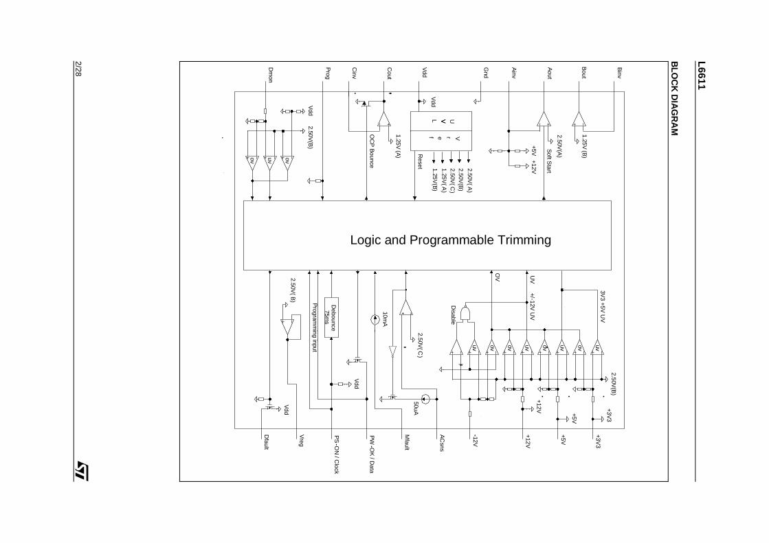
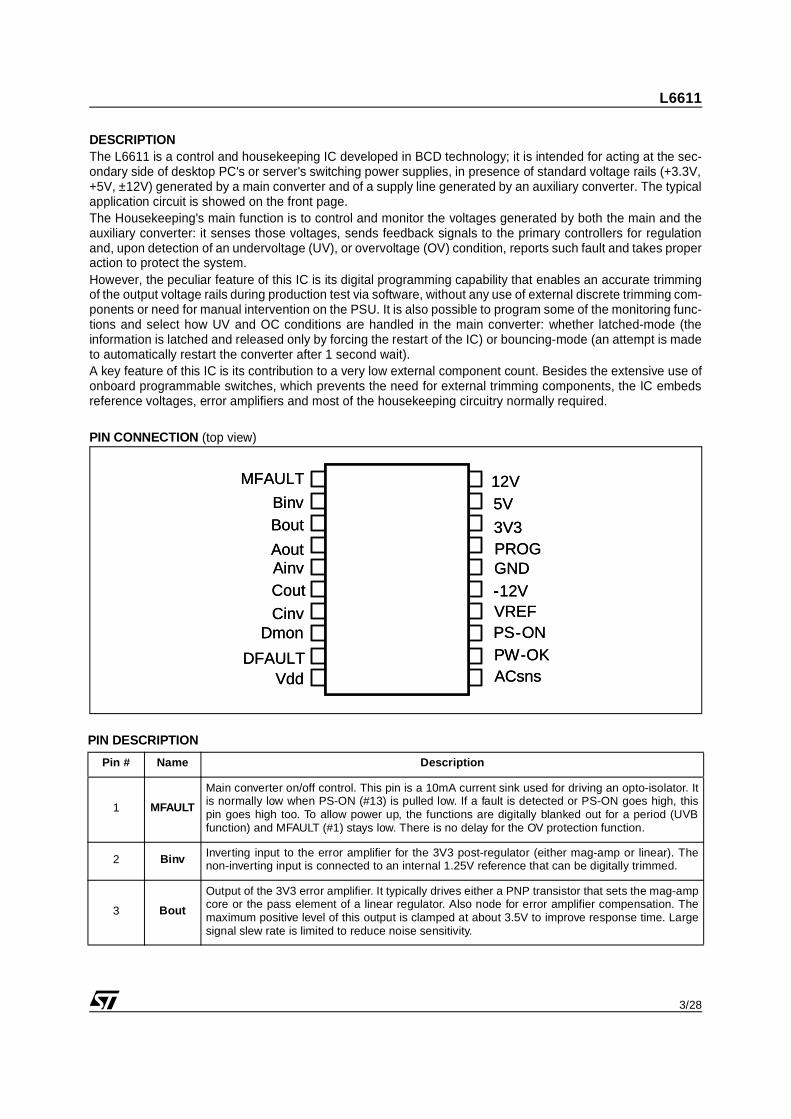
DESCRIPTIONThe L6611 is a control and housekeeping IC developed in BCD technology; it is intended for acting at the sec-ondary side of desktop PC's or server's switching power supplies, in presence of standard voltage rails (+3.3V,+5V, ±12V) generated by a main converter and of a supply line generated by an auxiliary converter. The typicalapplication circuit is showed on the front page.The Housekeeping's main function is to control and monitor the voltages generated by both the main and theauxiliary converter: it senses those voltages, sends feedback signals to the primary controllers for regulationand, upon detection of an undervoltage (UV), or overvoltage (OV) condition, reports such fault and takes properaction to protect the system. However, the peculiar feature of this IC is its digital programming capability that enables an accurate trimmingof the output voltage rails during production test via software, without any use of external discrete trimming com-ponents or need for manual intervention on the PSU. It is also possible to program some of the monitoring func-tions and select how UV and OC conditions are handled in the main converter: whether latched-mode (theinformation is latched and released only by forcing the restart of the IC) or bouncing-mode (an attempt is madeto automatically restart the converter after 1 second wait).A key feature of this IC is its contribution to a very low external component count. Besides the extensive use ofonboard programmable switches, which prevents the need for external trimming components, the IC embedsreference voltages, error amplifiers and most of the housekeeping circuitry normally required.
PIN CONNECTION (top view)
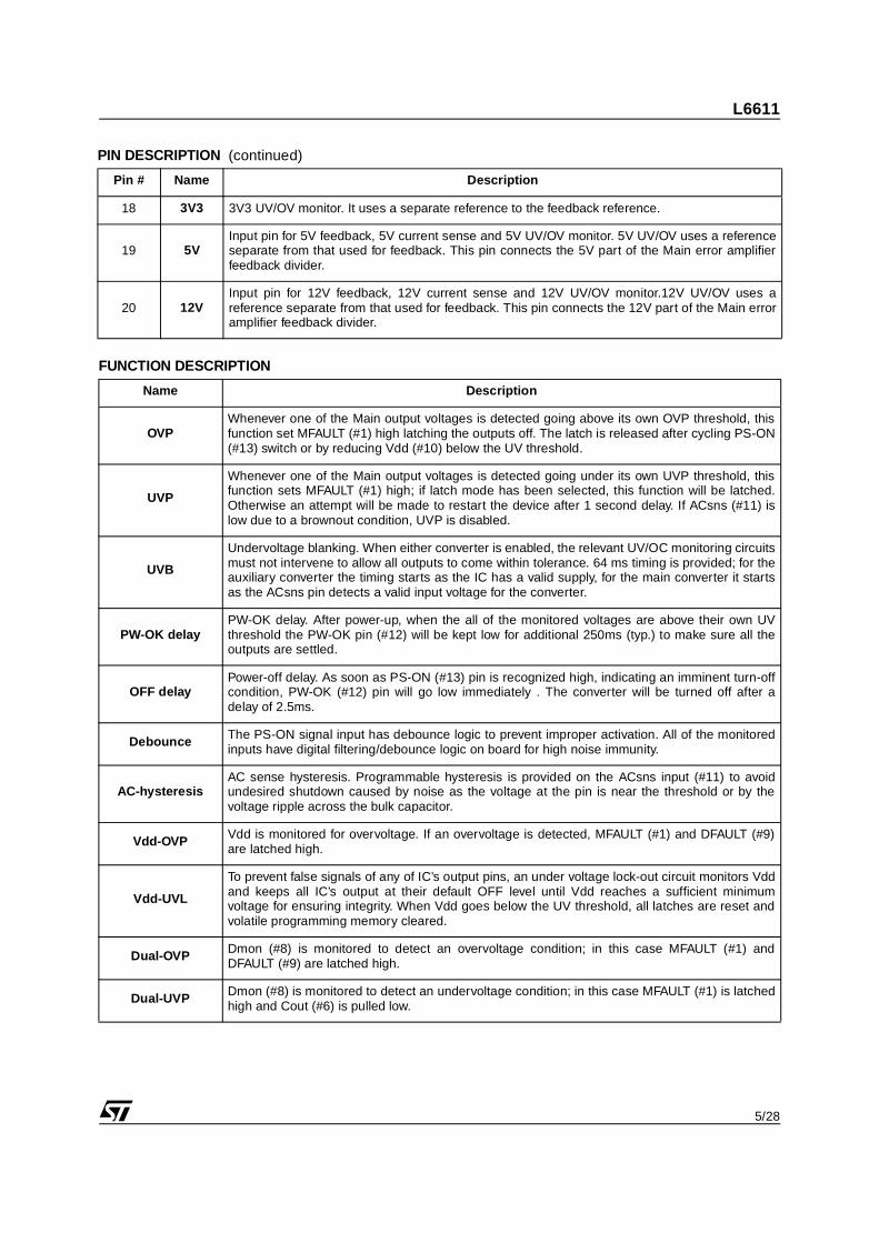
PIN DESCRIPTION
Pin # Name Description
1 MFAULT
Main converter on/off control. This pin is a 10mA current sink used for driving an opto-isolator. Itis normally low when PS-ON (#13) is pulled low. If a fault is detected or PS-ON goes high, thispin goes high too. To allow power up, the functions are digitally blanked out for a period (UVBfunction) and MFAULT (#1) stays low. There is no delay for the OV protection function.
2 Binv Inverting input to the error amplifier for the 3V3 post-regulator (either mag-amp or linear). Thenon-inverting input is connected to an internal 1.25V reference that can be digitally trimmed.
3 Bout
Output of the 3V3 error amplifier. It typically drives either a PNP transistor that sets the mag-ampcore or the pass element of a linear regulator. Also node for error amplifier compensation. Themaximum positive level of this output is clamped at about 3.5V to improve response time. Largesignal slew rate is limited to reduce noise sensitivity.
MFAULT
BinvBout
12V5V
3V3
-12VVREFPS-ONPW-OKACsnsVdd
DFAULT
Dmon
Cout
AoutAinv
PROG
Cinv
GND-
-
MFAULT
BinvBout
12V5V
3V3
-12VVREFPS-ONPW-OKACsnsVdd
DFAULT
Dmon
Cout
AoutAinv
PROG
Cinv
GND-
-
Obsolete Product(
s) - O
bsolete Product(
s)
Obsolete Product(
s) - O
bsolete Product(
s)
L6611
4/28
4 Aout Output of the error amplifier for the main converter. This pin typically drives an optocoupler and isalso used for compensation along with Ainv (pin #5).
5 Ainv
Main loop error amplifier inverting input. The non-inverting input is connected to an internal 2.5Vreference that can be digitally trimmed. A high impedance internal divider from +12V and +5VUV/OV sense pins (#19, #20) eliminates the need for external divider in most applications. Thepin is used for error amplifier compensation.
6 Cout Auxiliary loop optocoupler drive. Also node for error amp compensation. Large signal slew rate islimited to reduce sensitivity to switching noise.
7 Cinv Inverting input for Auxiliary error amplifier. The non-inverting input is connected to an internal1.25V reference that can be digitally trimmed.
8 DmonDual or Auxiliary UV/OV monitor, Dmon is programmable to monitor 3V3 or 5V. To allow a correctpower up, the UV function on this pin is blanked out during initial start-up. There is no delay forthe OV function.
9 DFAULTDual or Auxiliary fault protection. When Dmon (#8) recognizes an over voltage, DFAULT andMFAULT (#1) go high. DFAULT is capable of sourcing up to 50mA. Possible applications are acrowbar across the Auxiliary output or an opto-coupled fault signal to the primary side.
10 VddPositive input supply voltage. Vdd is normally supplied from the Auxiliary power supply outputvoltage. If Vdd-UVL detects a sustained under voltage, PW-OK (#12) will be pulled low andsending MFAULT (#1) high will disable the main converter.
11 ACsns
Analog of bulk voltage for AC fail warning. The usual source of this analog pin is one of thesecondary windings of the main transformer. Hysteresis is provided through a trimmable 50µAcurrent sink on this pin that is activated as the voltage at the pin falls below the internal reference(2.5V).
12PW-OK/Data
Power good signal for the Main converter. When asserted high, this pin indicates that thevoltages monitored are above their UV limits. There will be typically 250ms delay from the Mainoutputs becoming good and PW-OK being asserted. This is nominally an open drain signal. Toimprove robustness, this output has a limited current sink capability. In programming mode, thispin is used for data input; then the absolute maximum rating will be Vdd+0.5V.
13PS-ON /Clock
Control pin to enable the Main converter. This pin has debouncing logic. A recognized high valueon this pin will cause PW-OK (#12) to go immediately low and, after a delay of 2.5ms, to shutdown the main PWM by allowing MFAULT (#1) to go high. During normal operation (or if notused) this pin has to be connected to a voltage lower than 0.8V. In programming mode, this pinwill be used to clock serial data into the chip.
14 VREF2.5V reference for external applications. This is a buffered pin. Shorting this pin to ground or toVdd (#10) will not affect integrity of control or monitor references. An external capacitor (max.100nF) is required whenever the pin is loaded (up to 5 mA), otherwise it can be left floating.
15 -12V -12V UV/OV monitor. If connected to a voltage greater than 1.5V (e.g. VREF, #14), the functionwill be disabled.
16 GNDGround pin. The connection integrity of this pin is constantly monitored and in case of either abond wire or a PCB trace going open, MFAULT (#1) and DFAULT (#9) will be forced highswitching off the supply.
17 PROG
The chip has 2 operating modes, depending on PROG input pin biasing:– normal mode: PROG should be floating or shorted to ground;– programming mode: forcing PROG high (+5V), the chip enters programming mode. PW_OK
(#12) and PS_ON (#13) pins are disconnected from their normal functionality and they becomeinputs for DATA and CLOCK allowing the chip to be programmed. The programming mode al-lows selecting some options and adjusting some setpoints;
PIN DESCRIPTION (continued)
Pin # Name Description
Obsolete Product(
s) - O
bsolete Product(
s)
Obsolete Product(
s) - O
bsolete Product(
s)
5/28
L6611
18 3V3 3V3 UV/OV monitor. It uses a separate reference to the feedback reference.
19 5VInput pin for 5V feedback, 5V current sense and 5V UV/OV monitor. 5V UV/OV uses a referenceseparate from that used for feedback. This pin connects the 5V part of the Main error amplifierfeedback divider.
20 12VInput pin for 12V feedback, 12V current sense and 12V UV/OV monitor.12V UV/OV uses areference separate from that used for feedback. This pin connects the 12V part of the Main erroramplifier feedback divider.
FUNCTION DESCRIPTION
Name Description
OVPWhenever one of the Main output voltages is detected going above its own OVP threshold, thisfunction set MFAULT (#1) high latching the outputs off. The latch is released after cycling PS-ON(#13) switch or by reducing Vdd (#10) below the UV threshold.
UVP
Whenever one of the Main output voltages is detected going under its own UVP threshold, thisfunction sets MFAULT (#1) high; if latch mode has been selected, this function will be latched.Otherwise an attempt will be made to restart the device after 1 second delay. If ACsns (#11) islow due to a brownout condition, UVP is disabled.
UVB
Undervoltage blanking. When either converter is enabled, the relevant UV/OC monitoring circuitsmust not intervene to allow all outputs to come within tolerance. 64 ms timing is provided; for theauxiliary converter the timing starts as the IC has a valid supply, for the main converter it startsas the ACsns pin detects a valid input voltage for the converter.
PW-OK delayPW-OK delay. After power-up, when the all of the monitored voltages are above their own UVthreshold the PW-OK pin (#12) will be kept low for additional 250ms (typ.) to make sure all theoutputs are settled.
OFF delayPower-off delay. As soon as PS-ON (#13) pin is recognized high, indicating an imminent turn-offcondition, PW-OK (#12) pin will go low immediately . The converter will be turned off after adelay of 2.5ms.
Debounce The PS-ON signal input has debounce logic to prevent improper activation. All of the monitoredinputs have digital filtering/debounce logic on board for high noise immunity.
AC-hysteresisAC sense hysteresis. Programmable hysteresis is provided on the ACsns input (#11) to avoidundesired shutdown caused by noise as the voltage at the pin is near the threshold or by thevoltage ripple across the bulk capacitor.
Vdd-OVP Vdd is monitored for overvoltage. If an overvoltage is detected, MFAULT (#1) and DFAULT (#9)are latched high.
Vdd-UVL
To prevent false signals of any of IC’s output pins, an under voltage lock-out circuit monitors Vddand keeps all IC’s output at their default OFF level until Vdd reaches a sufficient minimumvoltage for ensuring integrity. When Vdd goes below the UV threshold, all latches are reset andvolatile programming memory cleared.
Dual-OVP Dmon (#8) is monitored to detect an overvoltage condition; in this case MFAULT (#1) andDFAULT (#9) are latched high.
Dual-UVP Dmon (#8) is monitored to detect an undervoltage condition; in this case MFAULT (#1) is latchedhigh and Cout (#6) is pulled low.
PIN DESCRIPTION (continued)
Pin # Name Description
Obsolete Product(
s) - O
bsolete Product(
s)
Obsolete Product(
s) - O
bsolete Product(
s)
L6611
6/28
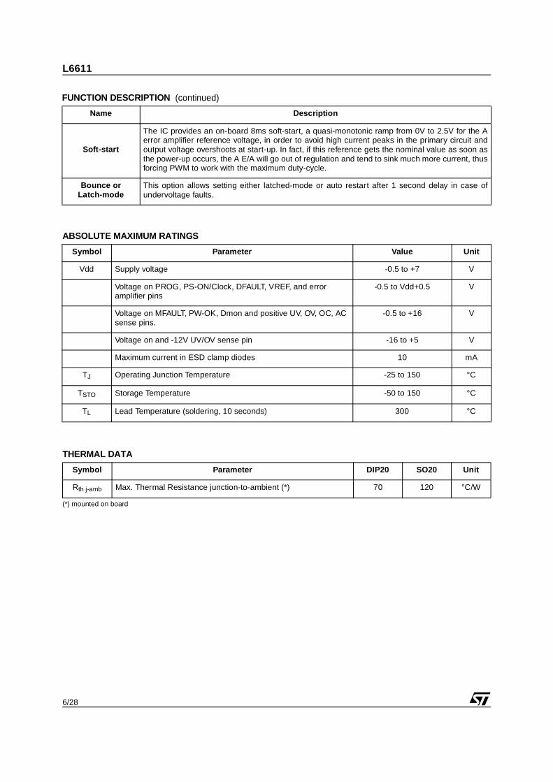
ABSOLUTE MAXIMUM RATINGS
THERMAL DATA
(*) mounted on board
Soft-start
The IC provides an on-board 8ms soft-start, a quasi-monotonic ramp from 0V to 2.5V for the Aerror amplifier reference voltage, in order to avoid high current peaks in the primary circuit andoutput voltage overshoots at start-up. In fact, if this reference gets the nominal value as soon asthe power-up occurs, the A E/A will go out of regulation and tend to sink much more current, thusforcing PWM to work with the maximum duty-cycle.
Bounce orLatch-mode
This option allows setting either latched-mode or auto restart after 1 second delay in case ofundervoltage faults.
Symbol Parameter Value Unit
Vdd Supply voltage -0.5 to +7 V
Voltage on PROG, PS-ON/Clock, DFAULT, VREF, and error amplifier pins
-0.5 to Vdd+0.5 V
Voltage on MFAULT, PW-OK, Dmon and positive UV, OV, OC, AC sense pins.
-0.5 to +16 V
Voltage on and -12V UV/OV sense pin -16 to +5 V
Maximum current in ESD clamp diodes 10 mA
TJ Operating Junction Temperature -25 to 150 °C
TSTO Storage Temperature -50 to 150 °C
TL Lead Temperature (soldering, 10 seconds) 300 °C
Symbol Parameter DIP20 SO20 Unit
Rth j-amb Max. Thermal Resistance junction-to-ambient (*) 70 120 °C/W
FUNCTION DESCRIPTION (continued)
Name Description
Obsolete Product(
s) - O
bsolete Product(
s)
Obsolete Product(
s) - O
bsolete Product(
s)
7/28
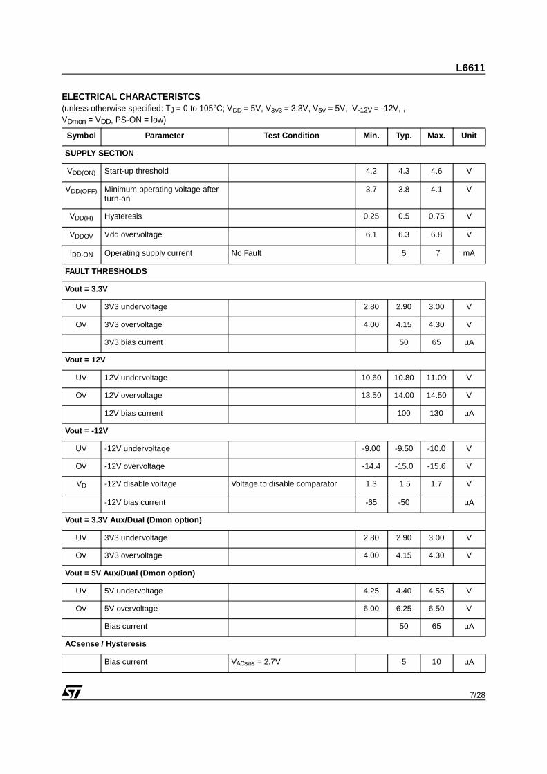
L6611
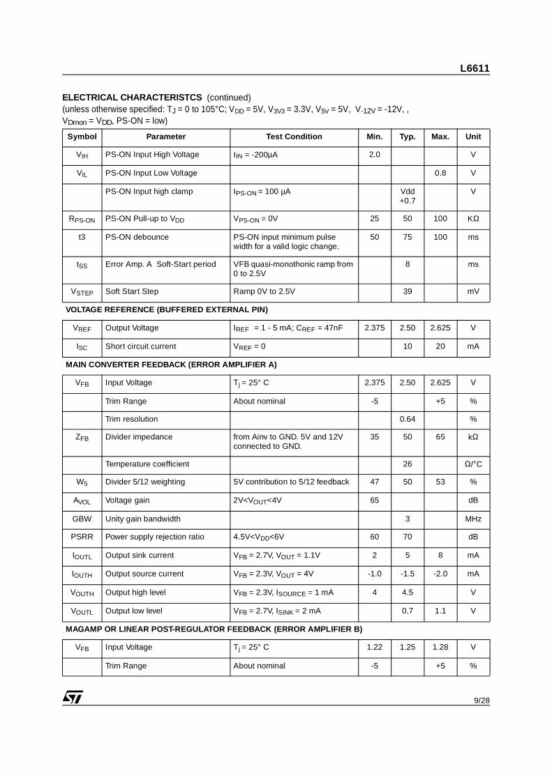
ELECTRICAL CHARACTERISTCS (unless otherwise specified: TJ = 0 to 105°C; VDD = 5V, V3V3 = 3.3V, V5V = 5V, V-12V = -12V, ,VDmon = VDD, PS-ON = low)
Symbol Parameter Test Condition Min. Typ. Max. Unit
SUPPLY SECTION
VDD(ON) Start-up threshold 4.2 4.3 4.6 V
VDD(OFF) Minimum operating voltage after turn-on
3.7 3.8 4.1 V
VDD(H) Hysteresis 0.25 0.5 0.75 V
VDDOV Vdd overvoltage 6.1 6.3 6.8 V
IDD-ON Operating supply current No Fault 5 7 mA
FAULT THRESHOLDS
Vout = 3.3V
UV 3V3 undervoltage 2.80 2.90 3.00 V
OV 3V3 overvoltage 4.00 4.15 4.30 V
3V3 bias current 50 65 µA
Vout = 12V
UV 12V undervoltage 10.60 10.80 11.00 V
OV 12V overvoltage 13.50 14.00 14.50 V
12V bias current 100 130 µA
Vout = -12V
UV -12V undervoltage -9.00 -9.50 -10.0 V
OV -12V overvoltage -14.4 -15.0 -15.6 V
VD -12V disable voltage Voltage to disable comparator 1.3 1.5 1.7 V
-12V bias current -65 -50 µA
Vout = 3.3V Aux/Dual (Dmon option)
UV 3V3 undervoltage 2.80 2.90 3.00 V
OV 3V3 overvoltage 4.00 4.15 4.30 V
Vout = 5V Aux/Dual (Dmon option)
UV 5V undervoltage 4.25 4.40 4.55 V
OV 5V overvoltage 6.00 6.25 6.50 V
Bias current 50 65 µA
ACsense / Hysteresis
Bias current VACsns = 2.7V 5 10 µA
Obsolete Product(
s) - O
bsolete Product(
s)
Obsolete Product(
s) - O
bsolete Product(
s)
L6611
8/28
UV AC undervoltage 2.375 2.50 2.625 V
Trim range -5 +5 %
Trim resolution 0.64 %
IACH Hysteresis current 20 50 80 µA
Hysteresis trim range -20 +20 %
HS Hysteresis adjust step 5 %
FAULT OUTPUTS
VPOKH PW-OK high state No faults 3 V
VPOKL PW-OK low state ISINK = 15mA 0.4 V
IL MFAULT high state leakage PS-ON = high 1 µA
MFISNK MFAULT sink current PS-ON = low, VMFAULT = 4V 6 10 15 mA
MFAULT OV debounce Minimum OV pulse before MFAULT is latched.
4 6 8 µs
MFAULT debounce±12V UV
Minimum UV pulse before MFAULT is latched.
4 6 8 µs
MFAULT debounce+5V, 3V3, UV
Minimum UV pulse before MFAULT is latched.
250 450 650 µs
DFIOH DFAULT output high source current
Overvoltage condition VDFAULT = 1.5V
-25 -50 -95 mA
DFVOH DFAULT output high voltage IDFAULT = 0mA, Tamb = 25oC, Overvoltage condition
2.1 2.4 2.7 V
VOUT DFAULT output low voltage IDFAULT = 1mA, no faults 0.3 0.5 0.7 V
DFAULT OV debounce Minimum OV pulse before DFAULT is latched.
4 6 8 µs
DFAULT UV debounce Minimum UV pulse before DFAULT is latched.
250 450 650 µs
START-UP / SHUTDOWN FUNCTIONS
t5 DFAULT UV blanking delay Delay from VDD(on) to DFAULT UV active.
44 64 84 ms
t1 MFAULT UV blanking delay Delay from ACSNS high to Main UV active
44 64 84 ms
t2 PW-OK blanking delay Main’s UV good to PW-OK high 175 250 325 ms
t4 (tDELAY)
PS-ON delay time Delay from PS-ON input to MFAULT
1.75 2.5 3.25 ms
ELECTRICAL CHARACTERISTCS (continued)(unless otherwise specified: TJ = 0 to 105°C; VDD = 5V, V3V3 = 3.3V, V5V = 5V, V-12V = -12V, ,VDmon = VDD, PS-ON = low)
Symbol Parameter Test Condition Min. Typ. Max. Unit
Obsolete Product(
s) - O
bsolete Product(
s)
Obsolete Product(
s) - O
bsolete Product(
s)
9/28
L6611
VIH PS-ON Input High Voltage IIN = -200µA 2.0 V
VIL PS-ON Input Low Voltage 0.8 V
PS-ON Input high clamp IPS-ON = 100 µA Vdd +0.7
V
RPS-ON PS-ON Pull-up to VDD VPS-ON = 0V 25 50 100 KΩ
t3 PS-ON debounce PS-ON input minimum pulse width for a valid logic change.
50 75 100 ms
tSS Error Amp. A Soft-Start period VFB quasi-monothonic ramp from 0 to 2.5V
8 ms
VSTEP Soft Start Step Ramp 0V to 2.5V 39 mV
VOLTAGE REFERENCE (BUFFERED EXTERNAL PIN)
VREF Output Voltage IREF = 1 - 5 mA; CREF = 47nF 2.375 2.50 2.625 V
ISC Short circuit current VREF = 0 10 20 mA
MAIN CONVERTER FEEDBACK (ERROR AMPLIFIER A)
VFB Input Voltage Tj = 25° C 2.375 2.50 2.625 V
Trim Range About nominal -5 +5 %
Trim resolution 0.64 %
ZFB Divider impedance from Ainv to GND. 5V and 12V connected to GND.
35 50 65 kΩ
Temperature coefficient 26 Ω/°C
W5 Divider 5/12 weighting 5V contribution to 5/12 feedback 47 50 53 %
AVOL Voltage gain 2V<VOUT<4V 65 dB
GBW Unity gain bandwidth 3 MHz
PSRR Power supply rejection ratio 4.5V<VDD<6V 60 70 dB
IOUTL Output sink current VFB = 2.7V, VOUT = 1.1V 2 5 8 mA
IOUTH Output source current VFB = 2.3V, VOUT = 4V -1.0 -1.5 -2.0 mA
VOUTH Output high level VFB = 2.3V, ISOURCE = 1 mA 4 4.5 V
VOUTL Output low level VFB = 2.7V, ISINK = 2 mA 0.7 1.1 V
MAGAMP OR LINEAR POST-REGULATOR FEEDBACK (ERROR AMPLIFIER B)
VFB Input Voltage Tj = 25° C 1.22 1.25 1.28 V
Trim Range About nominal -5 +5 %
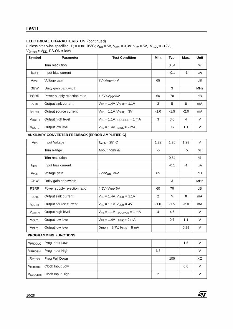
ELECTRICAL CHARACTERISTCS (continued)(unless otherwise specified: TJ = 0 to 105°C; VDD = 5V, V3V3 = 3.3V, V5V = 5V, V-12V = -12V, ,VDmon = VDD, PS-ON = low)
Symbol Parameter Test Condition Min. Typ. Max. Unit
Obsolete Product(
s) - O
bsolete Product(
s)
Obsolete Product(
s) - O
bsolete Product(
s)
L6611
10/28
Trim resolution 0.64 %
IBIAS Input bias current -0.1 -1 µA
AVOL Voltage gain 2V<VOUT<4V 65 dB
GBW Unity gain bandwidth 3 MHz
PSRR Power supply rejection ratio 4.5V<VDD<6V 60 70 dB
IOUTL Output sink current VFB = 1.4V, VOUT = 1.1V 2 5 8 mA
IOUTH Output source current VFB = 1.1V, VOUT = 3V -1.0 -1.5 -2.0 mA
VOUTH Output high level VFB = 1.1V, ISOURCE = 1 mA 3 3.6 4 V
VOUTL Output low level VFB = 1.4V, ISINK = 2 mA 0.7 1.1 V
AUXILIARY CONVERTER FEEDBACK (ERROR AMPLIFIER C)
VFB Input Voltage Tamb = 25° C 1.22 1.25 1.28 V
Trim Range About nominal -5 +5 %
Trim resolution 0.64 %
IBIAS Input bias current -0.1 -1 µA
AVOL Voltage gain 2V<VOUT<4V 65 dB
GBW Unity gain bandwidth 3 MHz
PSRR Power supply rejection ratio 4.5V<VDD<6V 60 70 dB
IOUTL Output sink current VFB = 1.4V, VOUT = 1.1V 2 5 8 mA
IOUTH Output source current VFB = 1.1V, VOUT = 4V -1.0 -1.5 -2.0 mA
VOUTH Output high level VFB = 1.1V, ISOURCE = 1 mA 4 4.5 V
VOUTL Output low level VFB = 1.4V, ISINK = 2 mA 0.7 1.1 V
VOUTL Output low level Dmon = 2.7V, ISINK = 5 mA 0.25 V
PROGRAMMING FUNCTIONS
VPROGLO Prog Input Low 1.5 V
VPROGHI Prog Input High 3.5 V
RPROG Prog Pull Down 100 KΩ
VCLOCKLO Clock Input Low 0.8 V
VCLOCKHI Clock Input High 2 V
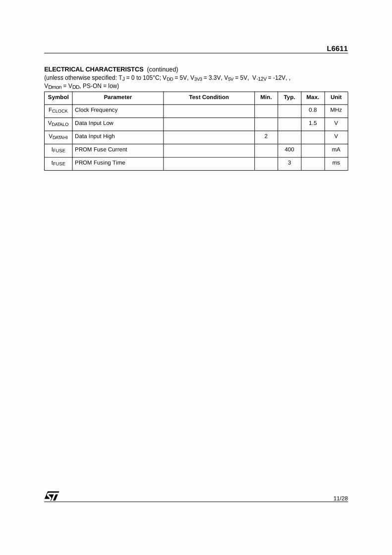
ELECTRICAL CHARACTERISTCS (continued)(unless otherwise specified: TJ = 0 to 105°C; VDD = 5V, V3V3 = 3.3V, V5V = 5V, V-12V = -12V, ,VDmon = VDD, PS-ON = low)
Symbol Parameter Test Condition Min. Typ. Max. Unit
Obsolete Product(
s) - O
bsolete Product(
s)
Obsolete Product(
s) - O
bsolete Product(
s)
11/28
L6611
FCLOCK Clock Frequency 0.8 MHz
VDATALO Data Input Low 1.5 V
VDATAHI Data Input High 2 V
IFUSE PROM Fuse Current 400 mA
tFUSE PROM Fusing Time 3 ms
ELECTRICAL CHARACTERISTCS (continued)(unless otherwise specified: TJ = 0 to 105°C; VDD = 5V, V3V3 = 3.3V, V5V = 5V, V-12V = -12V, ,VDmon = VDD, PS-ON = low)
Symbol Parameter Test Condition Min. Typ. Max. Unit
Obsolete Product(
s) - O
bsolete Product(
s)
Obsolete Product(
s) - O
bsolete Product(
s)
L6611
12/28
Figure 1. Supply start-up, UV and OV
Figure 2. IC Supply current vs. supply voltage
Figure 3. IC Supply current
Figure 4. Monitored inputs bias current
Figure 5. 3.3V fault thresholds
Figure 6. 5V fault thresholds
3.5
4.5
5.5
6.5
-50 -25 0 25 50 75 100 125 150
UV
start-up
over voltage
VDD [V]
T [OC]
VDD [V]0 2 4 6 8 10
0
2
4
6
8
10
IDD [mA]
Dmon = VDD
Tj = 25 °C
3
4
5
6
7
-50 -25 0 25 50 75 100 125 150
IDD [mA]
T [OC]
30
40
50
60
70
80
-50 -25 0 25 50 75 100 125 150
3.3Voutput
5Voutput
12Voutput
T [OC]
IB [µA]
2
3
4
5
-50 -25 0 25 50 75 100 125 150 T [OC]
undervoltage
overvoltage
V3.3V [V]
3
4
5
6
7
-50 -25 0 25 50 75 100 125 150 T [OC]
overvoltage
undervoltage
V5V [V]
TYPICAL ELECTRICAL CHARACTERISTICS
Obsolete Product(
s) - O
bsolete Product(
s)
Obsolete Product(
s) - O
bsolete Product(
s)
13/28
L6611
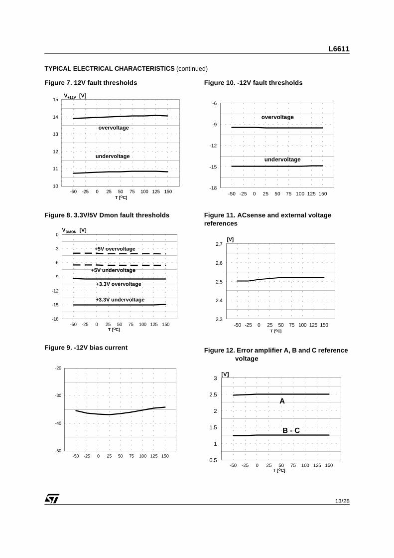
Figure 7. 12V fault thresholds
Figure 8. 3.3V/5V Dmon fault thresholds
Figure 9. -12V bias current
Figure 10. -12V fault thresholds
Figure 11. ACsense and external voltage references
Figure 12. Error amplifier A, B and C reference voltage
10
11
12
13
14
15
-50 -25 0 25 50 75 100 125 150 T [OC]
overvoltage
undervoltage
V+12V [V]
-18
-15
-12
-9
-6
-3
0
-50 -25 0 25 50 75 100 125 150
+3.3V undervoltage
+5V undervoltage
+5V overvoltage
+3.3V overvoltage
T [OC]
VDMON [V]
-50
-40
-30
-20
-50 -25 0 25 50 75 100 125 150
-18
-15
-12
-9
-6
-50 -25 0 25 50 75 100 125 150
overvoltage
undervoltage
2.3
2.4
2.5
2.6
2.7
-50 -25 0 25 50 75 100 125 150 T [OC]
[V]
0.5
1
1.5
2
2.5
3
-50 -25 0 25 50 75 100 125 150 T [OC]
[V]
A
B - C
TYPICAL ELECTRICAL CHARACTERISTICS (continued)
Obsolete Product(
s) - O
bsolete Product(
s)
Obsolete Product(
s) - O
bsolete Product(
s)
L6611
14/28
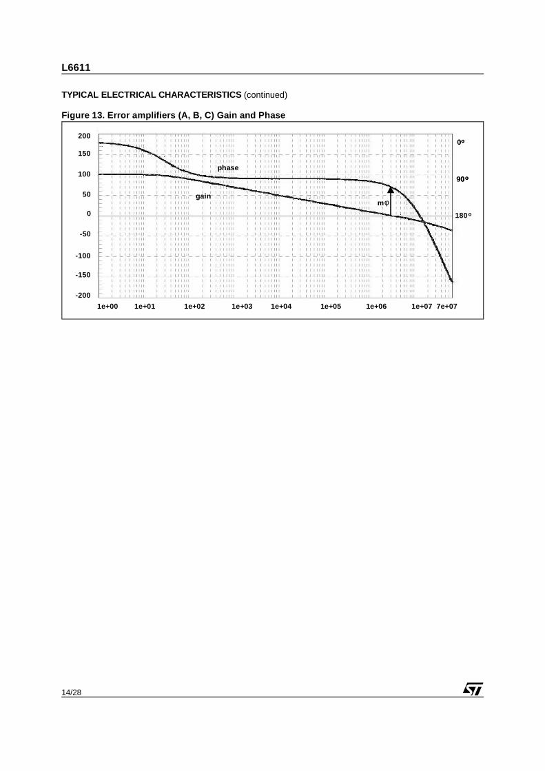
Figure 13. Error amplifiers (A, B, C) Gain and Phase
200
150
100
50
0
-50
-100
-150
-200
1e+00 1e+01 1e+02 1e+03 1e+04 1e+05 1e+06 1e+07 7e+07
90o
0o
mfgain
phase
200
150
100
50
0
-50
-100
-150
-200
1e+00 1e+01 1e+02 1e+03 1e+04 1e+05 1e+06 1e+07 7e+07
90o
0o
m φgain
phase
180o
TYPICAL ELECTRICAL CHARACTERISTICS (continued)
Obsolete Product(
s) - O
bsolete Product(
s)
Obsolete Product(
s) - O
bsolete Product(
s)
15/28
L6611
APPLICATION INFORMATION INDEX
1 On board digital trimming and mode selection..................................................................................Page 16
2 Error amplifiers and reference voltages ..................................................................................................... 18
Main section: error amplifier A and Soft -Start
E/A and reference voltage
3.3V section: error amplifier B
Auxiliary section: error amplifier C
3 Normal operation timing diagram ............................................................................................................... 20
4 Undervoltage, overvoltage and relevant timings ........................................................................................ 21
5 AC sense (mains undervoltage warning) ................................................................................................... 22
6 Application example ................................................................................................................................... 23
7 Application ideas ........................................................................................................................................ 25
Obsolete Product(
s) - O
bsolete Product(
s)
Obsolete Product(
s) - O
bsolete Product(
s)
L6611
16/28
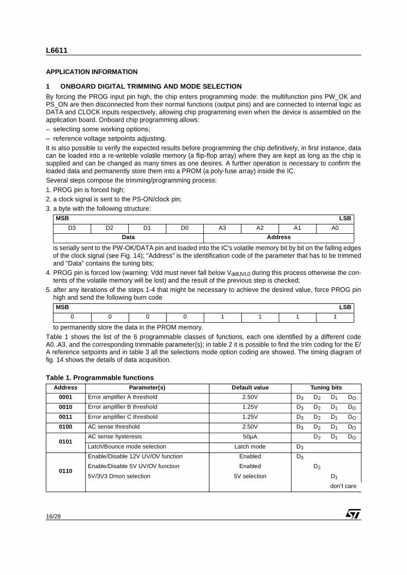
APPLICATION INFORMATION
1 ONBOARD DIGITAL TRIMMING AND MODE SELECTION
By forcing the PROG input pin high, the chip enters programming mode: the multifunction pins PW_OK andPS_ON are then disconnected from their normal functions (output pins) and are connected to internal logic asDATA and CLOCK inputs respectively, allowing chip programming even when the device is assembled on theapplication board. Onboard chip programming allows: – selecting some working options;– reference voltage setpoints adjusting. It is also possible to verify the expected results before programming the chip definitively, in first instance, datacan be loaded into a re-writeble volatile memory (a flip-flop array) where they are kept as long as the chip issupplied and can be changed as many times as one desires. A further operation is necessary to confirm theloaded data and permanently store them into a PROM (a poly-fuse array) inside the IC.Several steps compose the trimming/programming process:1. PROG pin is forced high;2. a clock signal is sent to the PS-ON/clock pin;3. a byte with the following structure:
is serially sent to the PW-OK/DATA pin and loaded into the IC's volatile memory bit by bit on the falling edgesof the clock signal (see Fig. 14); "Address" is the identification code of the parameter that has to be trimmedand "Data" contains the tuning bits;
4. PROG pin is forced low (warning: Vdd must never fall below VddUVL0 during this process otherwise the con-tents of the volatile memory will be lost) and the result of the previous step is checked;
5. after any iterations of the steps 1-4 that might be necessary to achieve the desired value, force PROG pinhigh and send the following burn code
to permanently store the data in the PROM memory.Table 1 shows the list of the 6 programmable classes of functions, each one identified by a different codeA0..A3, and the corresponding trimmable parameter(s); in table 2 it is possible to find the trim coding for the E/A reference setpoints and in table 3 all the selections mode option coding are showed. The timing diagram offig. 14 shows the details of data acquisition.
Table 1. Programmable functions
MSB LSB
D3 D2 D1 D0 A3 A2 A1 A0
Data Address
MSB LSB
0 0 0 0 1 1 1 1
Address Parameter(s) Default value Tuning bits
0001 Error amplifier A threshold 2.50V D3 D2 D1 DO
0010 Error amplifier B threshold 1.25V D3 D2 D1 DO
0011 Error amplifier C threshold 1.25V D3 D2 D1 DO
0100 AC sense threshold 2.50V D3 D2 D1 DO
0101AC sense hysteresis 50µA D2 D1 DO
Latch/Bounce mode selection Latch mode D3
0110
Enable/Disable 12V UV/OV function Enabled D3
Enable/Disable 5V UV/OV function Enabled D2
5V/3V3 Dmon selection 5V selection D1
don’t care
Obsolete Product(
s) - O
bsolete Product(
s)
Obsolete Product(
s) - O
bsolete Product(
s)
17/28
L6611
Table 2. Trim Coding
Table 3. Mode coding
Figure 14. Trimming/programming procedure: timing diagram
Parameter E/A A threshold2.5V typ.
E/A B threshold1.25V typ.
E/A C threshold1.25V typ.
ACsns threshold2.5V typ.
ACsns Hysteresys50µA typ.
Address 0001 0010 0011 0010 0101
Tuning BitsD3 D2 D1 D0
D3 D2 D1 D0∆V [mV]
D3 D2 D1 D0∆V [mV]
D3 D2 D1 D0∆V [mV]
D3 D2 D1 D0∆V [mV]
D2 D1 D0∆I [µA]
0 1 1 1 +112 +56 +56 +112
0 1 1 0 +96 +48 +48 +96
0 1 0 1 +80 +40 +40 +80
0 1 0 0 +64 +32 +32 +64
0 0 1 1 +48 +24 +24 +48 +7.5
0 0 1 0 +32 +16 +16 +32 +5.0
0 0 0 1 +16 +8 +8 +16 +2.5
0 0 0 0 0 0 0 0 0
1 1 1 1 -16 -8 -8 -16 -2.5
1 1 1 0 -32 -16 -16 -32 -5.0
1 1 0 1 -48 -24 -24 -48 -7.5
1 1 0 0 -64 -32 -32 -64 -10
1 0 1 1 -80 -40 -40 -80
1 0 1 0 -96 -48 -48 -96
1 0 0 1 -112 -56 -56 -112
1 0 0 0 -128 -64 -64 -128
Parameter Bounce or Latch Mode
Enable/Disable12V UV/OV
Enable/Disable5V UV/OV
5V/ 3.3V Dmon Selection
Address A3 A2 A1 A00101
A3 A2 A1 A00110
Bit Value
Tuning Bit
D3 D3 D2 D1
0 Latch Enabled Enabled 5V
1 Bounce Disabled Disabled 3.3V
10 0 00 01 1
MSB LSB
PROG
PS_ON/Clock
PW_OK/Data
Obsolete Product(
s) - O
bsolete Product(
s)
Obsolete Product(
s) - O
bsolete Product(
s)
L6611
18/28
2 ERROR AMPLIFIERS AND REFERENCE VOLTAGES
Three error amplifiers are implemented on the IC to achieve regulation of the output voltages: a brief descriptionfollows for each section.
– Main section: error amplifier A and Soft-Start.The circuit is designed to directly control the Main primary PWM through an optocoupler, providingvery good regulation and galvanic isolation from the primary side. Typical solutions require a shuntregulator, like the TL431, as a reference and feedback amplifier to sense the output voltage and gen-erate a corresponding error voltage; this voltage is then converted in a current transferred to the pri-mary side through the optocoupler.The feedback E/A amplifier is integrated in the IC: its non-inverting input is connected to an internally gen-erated voltage reference, whose default value is typically 2.5V. It can however be trimmed to obtain a betterprecision (see "On board trimming and mode operating" section). Then, no TL431 is needed.The E/A inverting input (Ainv, pin#5) and the E/A output (Aout, pin#4) are externally available and thefrequency compensation network (Zc) will be connected between them (see fig. 15).The high impedance (in the hundred kΩ) internal divider from 12V and 5V UV/OV sense pins elimi-nates the need for an external one in most applications, allowing a further reduction in the number ofexternal component. Under closed loop condition, the two upper branches, connected to 12V and 5V pins, supply equallythe current flowing through R3= 80.6K (equal to 2.5V/R3).In order to avoid high current peaks in the primary circuit and output voltage overshoots at start-up,the IC provides an on-board 8ms soft-start, a quasi-monotonic ramp from 0V to 2.5V for the A erroramplifier reference voltage,. In fact, if this reference gets the nominal value as soon as the power-upoccurs, the A E/A will go out of regulation and tend to sink much more current, thus forcing PWM towork with the maximum duty-cycle.
– E/A and references voltageBeing the inverting input of E/A externally available, it is possible to change the "weight" of the twocontributions or even eliminate one of them by connecting external resistors of much lower value (RL,RH1 and/or RH2 in fig. 15) that bypass the internal ones appropriately.For example using RL=2.4K, RH1=3.9K and RH2=24K, then the ratio between +5V and +12V outputweight will be equal to 6:4. By simply making RH1 = RL (for example 2.4K) with no RH2, only the +5V output is kept under feed-back because the contribution of +12V branch (through the internal 600K resistor) will be negligible.The pin #24 (12V) has to be connected to +12V output to guarantee the OV/UV monitoring.
Figure 15. Main feedback section
– 3.3V section, error amplifier B. It is the error amplifier used to set the magamp core through an external circuitry (see a typical sche-matic in figure 16). The non-inverting input of the error amplifier is connected to a trimmable 1.25V internal voltage ref-erence (see "On board trimming and mode operating" paragraph). The E/A inverting input is exter-nally available (Binv, pin#2) and is connected to the output divider (RH and RL); the output pin (Bout,
VDD
to MAINcontrol
Zc
Aout
RB
12V5V
+2.5V
600K168K
80.6K8ms SS
L6611 GND
_
+
+12V output
+5V output
Ainv
RL
RH1 RH2
optional, to change feedback weight
VDD
to MAINcontrol
Zc
Aout
RB
12V5V
+2.5V
600K168K
80.6K8ms SS
L6611 GND
_
+
+12V output
+5V output
Ainv
RL
RH1 RH2
optional, to change feedback weight
Obsolete Product(
s) - O
bsolete Product(
s)
Obsolete Product(
s) - O
bsolete Product(
s)
19/28
L6611
pin#3) drives the external circuitry that biases the magamp core. Between these pins it is connectedthe compensation network (ZC). The maximum positive output voltage is clamped at about 3.5V toimprove response time.The feedback control circuit determines the magamp "off" time, converting the voltage at the outputof error amplifier into a current IR, which resets the magamp. If the output voltage exceeds its presetvalue, V(Bout) decreases; this causes a higher voltage across RC which, in turn, implies a larger volt-age across RE and a larger reset current IR (VBE of Q1 is supposed constant). A larger IR causes thePWM waveform across D2 to get narrower. This pulls the output voltage back to the desired level andachieves regulation.It is possible to use this section to drive a pass transistor to obtain 3.3V with a linear regulator; in the"Application idea" section an example is showed to implement this solution.
Figure 16. Magamp control feedback section
– Auxiliary section, error amplifier C.This section (fig. 17) provides the feedback signal for the auxiliary converter following the same oper-ating principles as the Main section. The auxiliary output voltage (Vaux) is often defined as "Standbyvoltage" because the converter remains alive during standby condition (the Main converter is stopped)to supply the chip and all the ancillary circuits. Typical values for its output voltage are 5V or 3.3V.The inverting input (Cinv, pin#7) is connected to the output voltage through an external resistor dividerwhereas the non-inverting one is connected to a 1.25V trimmable internal voltage reference (see "Onboard trimming and mode operating" paragraph). The compensation network Zc(aux) is placed between E/A inverting input and output pins.When Dmon recognizes an undervoltage condition on the auxiliary output, an internal n-channel MOS(in open drain configuration) grounds E/A output pin; the high current flowing through the optocoupleris then transferred to the primary side causing a duty cycle as short as possible; this prevents a highenergy transfer from primary to secondary under short circuit conditions, thus reducing the thermalstress on the power components.
Figure 17. Auxiliary feedback section
+3.3V
Zc
BoutBinv
+1.25VRL
RH
_
+
L6611
magamp
RC
RS
RE
D1
IR
D2VD2
Q1
LC
+3.3V
Zc
BoutBinv
+1.25VRL
RH
_
+
L6611
magamp
RC
RS
RE
D1
IR
D2VD2
Q1
LC
VAUX
to AUXcontrol
Zc(aux)
Cout
Cinv
RB
+1.25V
RH
RL
_
+
L6611
OCP bounce
GND
DMON
VAUX
to AUXcontrol
Zc(aux)
Cout
Cinv
RB
+1.25V
RH
RL
_
+
L6611
OCP bounce
GND
DMON
Obsolete Product(
s) - O
bsolete Product(
s)
Obsolete Product(
s) - O
bsolete Product(
s)
L6611
20/28
3 NORMAL OPERATION TIMING DIAGRAM (FIG. 18)
The time intervals t1-t5 are listed below– t1: UV/OC blanking of MFAULT. While Main outputs are ramping up, the UV comparators are blanked
for this interval to prevent a false turn-off. No such blanking is applied to OV faults.– t2: PW-OK delay. This period starts when all monitored outputs and AC sense are above their respec-
tive UV levels and finishes at PW-OK going high.– t3: PS-ON debounce period. The voltage on PS-ON must be continuously present in a high or low state
for a minimum period for that state to be recognized.– t4: Tdelay. The time from PS-ON being recognized as going high to MFAULT going high. This is to
provide a power down warning. When PS-ON requests power off, PW-OK goes low immediately.– t5: UV blanking of DFAULT. During initial power up a period of UV blanking is applied to DFAULT as
soon as Vdd to the chip is in the correct range. No such blanking is applied to OV faults.
Figure 18. Normal Operation Timing Diagram (ON/OFF with PS-ON or the AC power switch).
AC
Vdd
PS-ON
Mfault
MainOPs
POK
UVBmfault
ACsns
Off
On
On
Off
t3
t1
t2 t4
t3
t2
t1
Vdd-ok
UVBdfault
ACsns_high ACsns_low
Vdd(on)Vdd(on)
t5
Obsolete Product(
s) - O
bsolete Product(
s)
Obsolete Product(
s) - O
bsolete Product(
s)
21/28
L6611
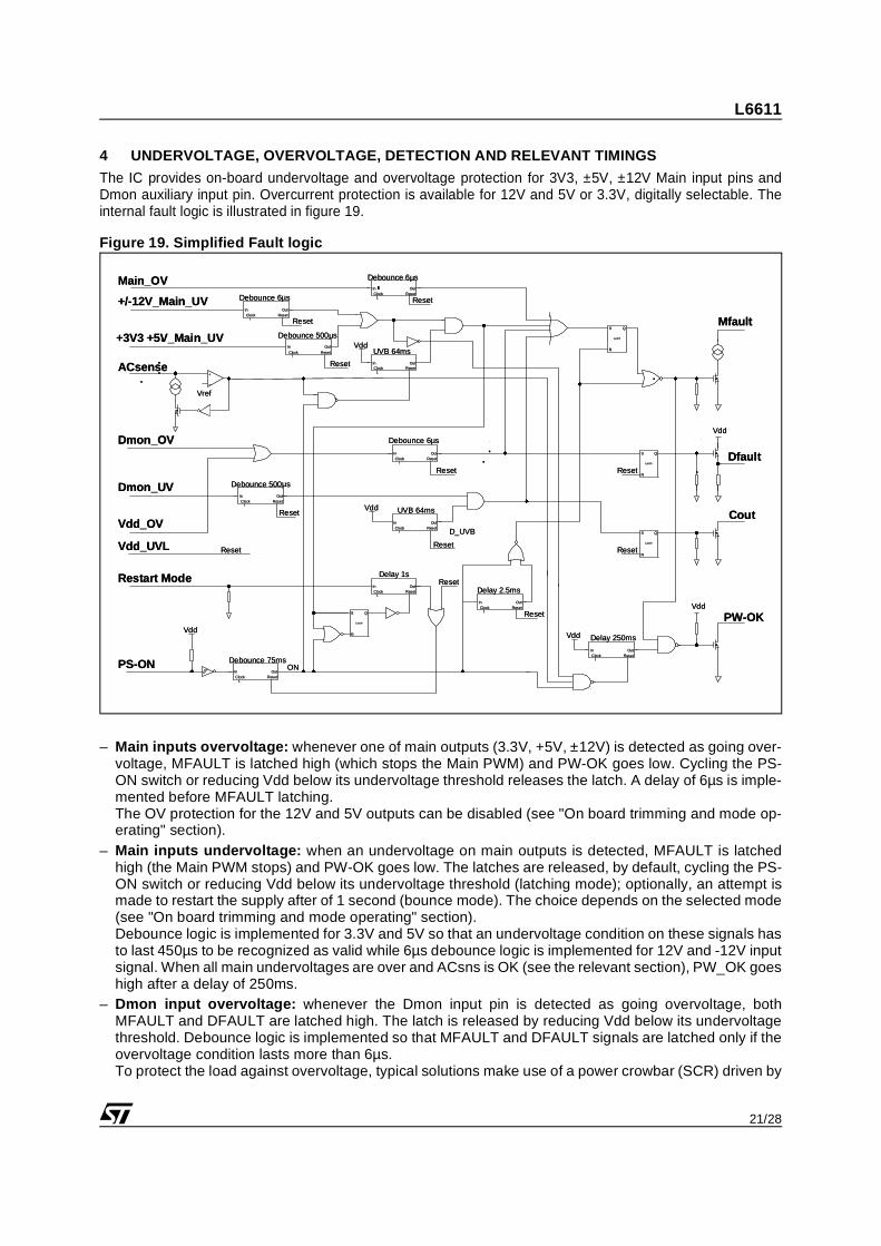
4 UNDERVOLTAGE, OVERVOLTAGE, DETECTION AND RELEVANT TIMINGS
The IC provides on-board undervoltage and overvoltage protection for 3V3, ±5V, ±12V Main input pins andDmon auxiliary input pin. Overcurrent protection is available for 12V and 5V or 3.3V, digitally selectable. Theinternal fault logic is illustrated in figure 19.
Figure 19. Simplified Fault logic
– Main inputs overvoltage: whenever one of main outputs (3.3V, +5V, ±12V) is detected as going over-voltage, MFAULT is latched high (which stops the Main PWM) and PW-OK goes low. Cycling the PS-ON switch or reducing Vdd below its undervoltage threshold releases the latch. A delay of 6µs is imple-mented before MFAULT latching.The OV protection for the 12V and 5V outputs can be disabled (see "On board trimming and mode op-erating" section).
– Main inputs undervoltage: when an undervoltage on main outputs is detected, MFAULT is latchedhigh (the Main PWM stops) and PW-OK goes low. The latches are released, by default, cycling the PS-ON switch or reducing Vdd below its undervoltage threshold (latching mode); optionally, an attempt ismade to restart the supply after of 1 second (bounce mode). The choice depends on the selected mode(see "On board trimming and mode operating" section).Debounce logic is implemented for 3.3V and 5V so that an undervoltage condition on these signals hasto last 450µs to be recognized as valid while 6µs debounce logic is implemented for 12V and -12V inputsignal. When all main undervoltages are over and ACsns is OK (see the relevant section), PW_OK goeshigh after a delay of 250ms.
– Dmon input overvoltage: whenever the Dmon input pin is detected as going overvoltage, bothMFAULT and DFAULT are latched high. The latch is released by reducing Vdd below its undervoltagethreshold. Debounce logic is implemented so that MFAULT and DFAULT signals are latched only if theovervoltage condition lasts more than 6µs.To protect the load against overvoltage, typical solutions make use of a power crowbar (SCR) driven by
Delay 1sInClock
OutReset
Debounce 75ms
ClockIn
ResetOut
PS-ON
Restart Mode
Vdd
Vdd_OV
Vdd_UVL
ON
Clock Reset
UVB 64msIn Out
Clock Reset
UVB 64msIn Out
Dmon_UV
Dmon_OV
ACsense
Vref
Main_OV
ResetClockIn Out
Debounce 6µs
ResetClockIn Out
ResetClockIn Out
Latch
R
S Q
ClockIn
ResetOut
Delay 250ms
Delay 2.5ms
ResetOut
ClockIn
Vdd
PW-OK
Cout
Latch
R
S Q
Latch
R
S Q
Dfault
Vdd
Mfault
Latch
R
S Q
Vdd
Vdd
Vdd
D_UVB
Reset
ResetClock
In Out
Reset
Reset
Reset
Reset
ResetReset
Reset
Reset
Reset
Reset
ResetClockIn Out
+/-12V_Main_UV
+3V3 +5V_Main_UV
Debounce 6µs
Debounce 500µs
Debounce 500µs
Debounce 6µs
+
Obsolete Product(
s) - O
bsolete Product(
s)
Obsolete Product(
s) - O
bsolete Product(
s)
L6611
22/28
DFAULT; in the "Application ideas" section, another simple circuit is showed to guarantee the same pro-tection without the SCR.
– Dmon input undervoltage: when an undervoltage on Dmon is detected, MFAULT is put high, Cout ispulled low (an internal OCP_BOUNCE signal is generated, see fig. 19) and PW_OK falls down. Thisfunction is enabled 64ms after the UVLO signal falls down. Debounce logic is implemented so thatMFAULT and OCP_BOUNCE signals are generated only if the undervoltage condition lasts more than500µs.The Dmon UV and OV protections can be set to work with thresholds set for 5V or 3.3V output voltage:the choice depends on the IC programming.
Figure 20. Fault timing diagram
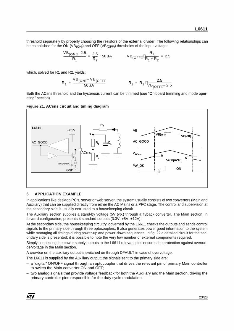
5 AC SENSE (MAINS UNDERVOLTAGE WARNING)
The device monitors the primary bulk voltage and warns the system when the power is about to be lost pullingdown the PW_OK output.The ACsns pin is typically connected to one of the windings of the main transformer (see fig. 21). Through asingle-diode rectification filter, a voltage equal to VB = VBULK/N (where VBULK is the voltage across the bulk ca-pacitor on primary side and N is the transformer turn ratio) is present at point B. A resistor (RF) could be usefulto clamp voltage spikes present.The fault signal is generated by means of AC_GOOD, the output of an internal comparator; this comparator isinternally referred to a trimmable 2.5V reference and indicates an AC fault if the voltage applied at its externallyavailable (non-inverting) input is below the internal reference, as shown in fig. 21. This comparator is provided with current hysteresis instead of a more usual voltage hysteresis: an internal 50µAcurrent generator is ON if the voltage is below 2.5V and is turned off when the voltage applied at the non-invert-ing input exceeds 2.5V. This approach provides an additional degree of freedom: it is possible to set the ON threshold and the OFF
Dmon(*)Dmon(*)
MfaultMfault
POKPOK
Dfault current Cout
Output
Mfault
POK
Main output’s overvoltage
Output
Mfault
POK
Main output’s undervoltage
Auxiliary output’s overvoltage Auxiliary output’s undervoltage
(*) Dmon is connected to the Auxiliary output Rail
Obsolete Product(
s) - O
bsolete Product(
s)
Obsolete Product(
s) - O
bsolete Product(
s)
23/28
L6611
threshold separately by properly choosing the resistors of the external divider. The following relationships canbe established for the ON (VB(ON)) and OFF (VB(OFF)) thresholds of the input voltage:
which, solved for R1 and R2, yields:
Both the ACsns threshold and the hysteresis current can be trimmed (see "On board trimming and mode oper-ating" section).
Figure 21. ACsns circuit and timing diagram
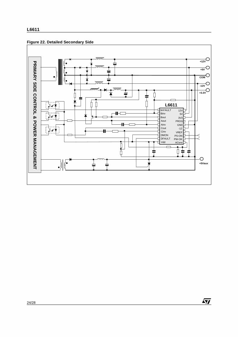
6 APPLICATION EXAMPLE
In applications like desktop PC's, server or web server, the system usually consists of two converters (Main andAuxiliary) that can be supplied directly from either the AC Mains or a PFC stage. The control and supervision atthe secondary side is usually entrusted to a housekeeping circuit.The Auxiliary section supplies a stand-by voltage (5V typ.) through a flyback converter. The Main section, inforward configuration, presents 4 standard outputs (3.3V, +5V, ±12V).At the secondary side, the housekeeping circuitry governed by the L6611 checks the outputs and sends controlsignals to the primary side through three optocouplers. It also generates power good information to the systemwhile managing all timings during power-up and power-down sequences. In fig. 22 a detailed circuit for the sec-ondary side is presented; it is possible to note the very low number of external components required.Simply connecting the power supply outputs to the L6611 relevant pins ensures the protection against over/un-dervoltage in the Main section.A crowbar on the auxiliary output is switched on through DFAULT in case of overvoltage.The L6611 is supplied by the Auxiliary output; the signals sent to the primary side are:– a "digital" ON/OFF signal through an optocoupler that drives the relevant pin of primary Main controller
to switch the Main converter ON and OFF;– two analog signals that provide voltage feedback for both the Auxiliary and the Main section, driving the
primary controller pins responsible for the duty cycle modulation.
VB ON( ) 2.5–
R1---------------------------------- 2.5
R2-------- 50µA+= VB OFF( )
R2
R1 R2+--------------------⋅ 2.5=
R1
VB ON( ) VB OFF( )–
50µA-------------------------------------------------= R2 R1
2.5VB OFF( ) 2.5–-------------------------------------⋅=
+2.5V
GND
IHYS=50µA
_
+
AC_GOOD R1
R2
C1
RF
B
L6611
ACsns
VB
AC_GOOD
VACsns
VB(on) VB(off)
∆=50µA*R1
∆∆
PW_OKON
+2.5V
GND
IHYS=50µA
_
+
AC_GOOD R1
R2
C1
RF
B
L6611
ACsns
VB
AC_GOOD
VACsns
VB(on) VB(off)
∆=50µA*R1
∆∆
PW_OKON
Obsolete Product(
s) - O
bsolete Product(
s)
Obsolete Product(
s) - O
bsolete Product(
s)
L6611
24/28
Figure 22. Detailed Secondary Side
+5Vaux
+5V
+12V
COM
-12V
+3.3V
-12
3V3
DMON
12V5V
Bout
BinvM-FAULT
AinvCout
PS-ON
Cinv VREF
Aout
Vdd ACsns
DFAULT PW-OK
GND
PR
IMA
RY
SID
E C
ON
TR
OL &
PO
WE
R M
AN
AG
EM
EN
T
L6611
PROG
Obsolete Product(
s) - O
bsolete Product(
s)
Obsolete Product(
s) - O
bsolete Product(
s)
25/28
L6611
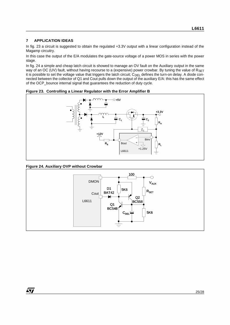
7 APPLICATION IDEAS
In fig. 23 a circuit is suggested to obtain the regulated +3.3V output with a linear configuration instead of theMagamp circuitry.In this case the output of the E/A modulates the gate-source voltage of a power MOS in series with the powerstage.In fig. 24 a simple and cheap latch circuit is showed to manage an OV fault on the Auxiliary output in the sameway of an OC (UV) fault, without having recourse to a (expensive) power crowbar. By tuning the value of RSETit is possible to set the voltage value that triggers the latch circuit; CDEL defines the turn-on delay. A diode con-nected between the collector of Q1 and Cout pulls down the output of the auxiliary E/A: this has the same effectof the OCP_bounce internal signal that guarantees the reduction of duty cycle.
Figure 23. Controlling a Linear Regulator with the Error Amplifier B
Figure 24. Auxiliary OVP without Crowbar
+3.3V
BoutBinv
+1.25V
RL
RH
_
+
L6611
+5V
RB
LC1 C2
+12V
ZC
+3.3V
BoutBinv
+1.25V
RL
RH
_
+
L6611
+5V
RB
LC1 C2
+12V
ZC
L6611
VAUXDMON
100
5K6
5K6
Q2BC558
Q1BC548
RSET
CDEL
Cout
D1BAT42
L6611
VAUXDMON
100
5K6
5K6
Q2BC558
Q1BC548
RSET
CDEL
Cout
D1BAT42
Obsolete Product(
s) - O
bsolete Product(
s)
Obsolete Product(
s) - O
bsolete Product(
s)
L6611
26/28
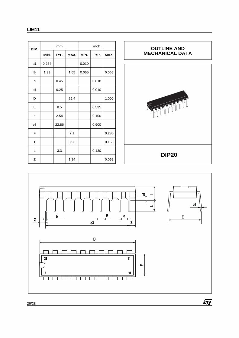
DIP20
DIM.mm inch
MIN. TYP. MAX. MIN. TYP. MAX.
a1 0.254 0.010
B 1.39 1.65 0.055 0.065
b 0.45 0.018
b1 0.25 0.010
D 25.4 1.000
E 8.5 0.335
e 2.54 0.100
e3 22.86 0.900
F 7.1 0.280
I 3.93 0.155
L 3.3 0.130
Z 1.34 0.053
OUTLINE ANDMECHANICAL DATA
Obsolete Product(
s) - O
bsolete Product(
s)
Obsolete Product(
s) - O
bsolete Product(
s)
27/28
L6611
1 10
1120
A
eB
D
E
L
K
H
A1 C
SO20MEC
h x 45˚
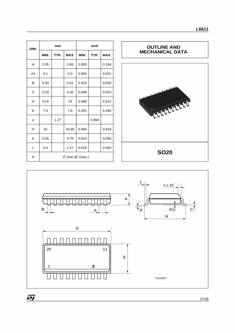
SO20
DIM.mm inch
MIN. TYP. MAX. MIN. TYP. MAX.
A 2.35 2.65 0.093 0.104
A1 0.1 0.3 0.004 0.012
B 0.33 0.51 0.013 0.020
C 0.23 0.32 0.009 0.013
D 12.6 13 0.496 0.512
E 7.4 7.6 0.291 0.299
e 1.27 0.050
H 10 10.65 0.394 0.419
h 0.25 0.75 0.010 0.030
L 0.4 1.27 0.016 0.050
K 0 (min.)8 (max.)
OUTLINE ANDMECHANICAL DATA
Obsolete Product(
s) - O
bsolete Product(
s)
Obsolete Product(
s) - O
bsolete Product(
s)
Information furnished is believed to be accurate and reliable. However, STMicroelectronics assumes no responsibility for the consequencesof use of such information nor for any infringement of patents or other rights of third parties which may result from its use. No license is grantedby implication or otherwise under any patent or patent rights of STMicroelectronics. Specifications mentioned in this publication are subjectto change without notice. This publication supersedes and replaces all information previously supplied. STMicroelectronics products are notauthorized for use as critical components in life support devices or systems without express written approval of STMicroelectronics.
The ST logo is a registered trademark of STMicroelectronics 2002 STMicroelectronics - All Rights Reserved
STMicroelectronics GROUP OF COMPANIESAustralia - Brazil - Canada - China - Finland - France - Germany - Hong Kong - India - Israel - Italy - Japan - Malaysia - Malta - Morocco -
Singapore - Spain - Sweden - Switzerland - United Kingdom - United States.http://www.st.com
28/28
L6611