Embed Size (px)
Citation preview
Subcontract Report NREL/SR-520-45545 April 2009
Processing Materials Devices and Diagnostics for Thin Film Photovoltaics: Fundamental and Manufacturability Issues Final Report 1 March 2005 – 30 November 2008 R.W. Birkmire, W.N. Shafarman, E. Eser, S.S. Hegedus, B.E. McCandless, K.D. Dobson, and S. Bowden University of Delaware Newark, Delaware

National Renewable Energy Laboratory 1617 Cole Boulevard, Golden, Colorado 80401-3393 303-275-3000 • www.nrel.gov
NREL is a national laboratory of the U.S. Department of Energy Office of Energy Efficiency and Renewable Energy Operated by the Alliance for Sustainable Energy, LLC
Contract No. DE-AC36-08-GO28308
Subcontract Report NREL/SR-520-45545 April 2009
Processing Materials Devices and Diagnostics for Thin Film Photovoltaics: Fundamental and Manufacturability Issues Final Report 1 March 2005 – 30 November 2008 R.W. Birkmire, W.N. Shafarman, E. Eser, S.S. Hegedus, B.E. McCandless, K.D. Dobson, and S. Bowden University of Delaware Newark, Delaware
NREL Technical Monitor: Bolko von Roedern Prepared under Subcontract No. ADJ-1-30630-12
This publication was reproduced from the best available copy submitted by the subcontractor and received no editorial review at NREL
NOTICE
This report was prepared as an account of work sponsored by an agency of the United States government. Neither the United States government nor any agency thereof, nor any of their employees, makes any warranty, express or implied, or assumes any legal liability or responsibility for the accuracy, completeness, or usefulness of any information, apparatus, product, or process disclosed, or represents that its use would not infringe privately owned rights. Reference herein to any specific commercial product, process, or service by trade name, trademark, manufacturer, or otherwise does not necessarily constitute or imply its endorsement, recommendation, or favoring by the United States government or any agency thereof. The views and opinions of authors expressed herein do not necessarily state or reflect those of the United States government or any agency thereof.
Available electronically at http://www.osti.gov/bridge
Available for a processing fee to U.S. Department of Energy and its contractors, in paper, from:
U.S. Department of Energy Office of Scientific and Technical Information P.O. Box 62 Oak Ridge, TN 37831-0062 phone: 865.576.8401 fax: 865.576.5728 email: mailto:[email protected]
Available for sale to the public, in paper, from: U.S. Department of Commerce National Technical Information Service 5285 Port Royal Road Springfield, VA 22161 phone: 800.553.6847 fax: 703.605.6900 email: [email protected] online ordering: http://www.ntis.gov/ordering.htm
Printed on paper containing at least 50% wastepaper, including 20% postconsumer waste

iii
List of Contributors
Principal Investigators Roger Aparicio Robert Birkmire Stuart Bowden Ujjwal Das Kevin Dobson Erten Eser Steven Hegedus Brian McCandless William Shafarman
Researchers Wayne Buchanan Shannon Fields Gregory Hanket Andrew McDermott
Visiting Scholars/Scientists Vivian Alberts, Rand Afrikaans Univ., S. Africa Matt Edwards, Univ. of New South Wales Donghwan Kim, Korea Takashi Minemoto, Japan Cheikh Sene, Senegal Na Wei, Univ. of Stuttgart, China Datao Xie, China
Post-Doctoral Fellows/Limited Term Researcher
Stuart Bowden Estela Calixto-Rodriguez Ujjwal Das Mario Gossla Gautam Ganguly Jonathan Frey Moses Haimbodi Gregory Hanket Sukti Hazra Yunhe Huang Kyoung Kim Sylvain Marsillac Takashi Minemoto Shiro Nishiwaki

iv
Puthar Devassey Paulson Sergey Rykov Baosheng Sang Nick Smith Alex Stavrides Udai Singh
Technical Support Joshua Cadoret Charles Debo Vicky Dinetta Ronald Dozier Shannon Fields Kevin Hart Thomas Hughes-Lampros Dan Ryan
Graduate Students
Michael Burrows Darshini Desai Jeff Doody Ozgenc Ebil Dan Esposito Xin Fan Jonathan Frey Moses Haimbodi Rong Xue Huang Mike Humbert Toby Junker Rui Kamada Pengcheng Lv Meijun Lu Kapil Mukati Sarah Rickman Brent Shu Scott Stephens Jochen Titus Christopher Thompson James Wilson Eva Wu Dong Xu Clifford Yapp Mike Zellner

v
Undergraduate Students John Allen Michael Angelo Sirinivasan Balakrishnan Tyreef Bevel Derek Birkmire Joshua Cadoret William Crandley Brad Culver Andrew Damiani John Dellose Stephanie Einstein Grant Fisher Jonathan Frey Jennifer Griffith Yannick Goue Sonam Gupta Juanita Jablasone Brian Kennedy Mary Kondos Timothy Miller Kunal Modi Adam Murauskas Adam Palanker Laura Robinson Dan Ryan Dan Sadowsky Chelsea Saunders David Silowka Kevin Tran Brian Wagner Haoshu Wang James Wilson Chati Zony
Document Preparation Linda Granger Steven Hegedus L. Bonnie Johnston Elaine Koronik Teresa Sharp Tritt
Table of Contents
Page List of Contributors ............................................................................................................ iii
Table of Contents ............................................................................................................... vi
Abstract ............................................................................................................................ viii
1 Objectives, Training, and Publications ....................................................................1
1.1 CdTe/CdSe-based Solar Cells ............................................................................1
1.2 CuInSe2-based Solar Cells .................................................................................1
1.3 Si-based Solar Cells ...........................................................................................1
1.4 In-line Diagnostics .............................................................................................3
1.5 Training and Education ......................................................................................4
1.6 Publications ........................................................................................................4
1.7 Thin Film Partnership ........................................................................................4
1.8 Organization of the Report .................................................................................4
2 CdTe Based Solar Cells ...........................................................................................5
2.1 Phase 1 Summary: 9/5/01 to 9/4/02 ..................................................................5
2.2 Phase 2 Summary: 9/5/02 to 9/4/03 ................................................................10
2.3 Phase 3 Summary: 9/5/03 to 9/4/04 ................................................................13
2.4 Phase 4 Summary: 9/5/04 to 9/4/05 ................................................................17
2.5 Phase 5 Summary: 9/5/05 to 3/31/07 ..............................................................20
2.6 Phase 6 Summary: 4/1/07 to 12/31/07 ............................................................22
2.7 Phase 7 Summary: 1/1/08 to 5/31/08 ..............................................................23
2.8 References ........................................................................................................38
3 CIS-based Solar Cells ............................................................................................39
3.1 Phase 1 Summary: 9/5/01 to 9/4/02 ................................................................39
3.2 Phase 2 Summary: 9/5/02 to 9/4/03 ................................................................41
3.3 Phase 3 Summary: 9/5/03 to 9/4/04 ................................................................43
3.4 Phase 4 Summary: 9/5/04 to 9/4/05 ................................................................45
vi

3.5 Phase 5 Summary: 9/5/05 to 3/31/07 ..............................................................49
3.6 Phase 6 Summary: 4/1/07 to 12/31/07 ............................................................52
3.7 Phase 7 Summary: 1/1/08 to 5/31/08 ..............................................................54
3.8 References ........................................................................................................61
4 Si-Based Solar Cells ..............................................................................................62
4.1 Phase 1 Summary: 9/5/01 to 9/4/02 ................................................................62
4.2 Phase 2 Summary: 9/5/02 to 9/4/03 ................................................................64
4.3 Phase 3 Summary: 9/5/03 to 9/4/04 ................................................................66
4.4 Phase 4 Summary: 9/5/04 to 9/4/05 ................................................................69
4.5 Phase 5 Summary: 9/5/05 to 3/31/07 ..............................................................69
4.6 Phase 6 Summary: 4/1/07 to 12/31/07 ............................................................71
4.7 Phase 7 Summary: 1/1/08 to 5/31/08 ..............................................................72
5 In-Line Diagnostics and Process Control ..............................................................80
5.1 Phase 1 Summary: 9/5/01 to 9/4/02 ................................................................80
5.2 Phase 2 Summary: 9/5/02 to 9/4/03 ................................................................80
5.3 Phase 3 Summary: 9/5/03 to 9/4/04 ................................................................81
5.4 Phase 4 Summary: 9/5/04 to 9/4/05 ................................................................82
5.5 Phase 5 Summary: 9/5/05 to 3/31/07 ..............................................................82
5.6 Phase 6 Summary: 4/1/07 to 12/31/07 ............................................................83
6 Publications ............................................................................................................85
vii
viii
Abstract
This report describes results achieved under this subcontract to develop and understand thin film solar cell technology associated to CuInSe2 and related alloys, a-Si and its alloys and CdTe. This includes application of a-Si to c-Si wafer-type cells as well. Modules based on all these thin films are promising candidates to meet DOE long-range efficiency, reliability and manufacturing cost goals. The critical issues being addressed under this program are intended to provide the science and engineering basis for the development of viable commercial processes and to improve module performance. The generic research issues addressed are: 1) quantitative analysis of processing steps to provide information for efficient commercial scale equipment design and operation; 2) device characterization relating the device performance to materials properties and process conditions; 3) development of alloy materials with different bandgaps to allow improved device structures for stability and compatibility with module design; 4) development of improved window/heterojunction layers and contacts to improve device performance and reliability; and 5) evaluation of cell stability with respect to illumination, temperature and ambient and with respect to device structure and module encapsulation.
1
1 OBJECTIVES, TRAINING, AND PUBLICATIONS The primary objectives of the NREL-sponsored research at the Institute of Energy Conversion (IEC) research are listed below according to the specific 3 types of thin film solar cells currently under commercial interest. In addition, generic process diagnostic and control tools will be developed. Student training and publication statistics are also summarized.
1.1 CdTe/CdSe-based Solar Cells The CdTe effort will address increased voltage and stability, the development of an in-line CdTe process to implement high rate and high throughput deposition on a moving substrate, and fundamental studies of CdTe surface chemistry. To meet these objectives, IEC will:
• Separate and quantify the effect on VOC of high resistance (HR) buffer layers such as Ga2O3 and In2O3 and widening the CdS window layer bandgap with Zn.
• Develop and apply a transparent back contact to CdTe to probe back contact
junction formation and degradation.
• Evaluate methods for increasing VOC by reducing space charge recombination.
• Conduct detailed analysis of collection losses using conventional and bifacial devices, AMPS modeling, and JV measurements under different conditions.
• Improve the stability of CdTe devices by developing alternative processing steps
to ‘stabilize’ the junction and contact; and to compare the effects of well-controlled stress conditions on CdTe solar cells by performing detailed device analysis and relating results to differences in fabrication.
• Develop the fundamental understanding needed for high throughput CdTe module
fabrication by controlling high rate delivery of Cd and Te species to the moving substrate surface.
• Develop rapid and reproducible post-deposition processing alternatives to the
current CdCl2 vapor treatment.
• Determine fundamental understanding of etching and wet processing steps on CdTe surfaces
• Determine relation between the contact processing and CdTe surface chemistry,
and the device performance and stability especially as applies to First Solar devices.
2
1.2 CuInSe2-based Solar Cells The CuInSe2-based effort will characterize fundamental properties of interfaces in CuInSe2-based solar cells, develop approaches to improving VOC including alloying with S and Al, and will also include the development of an in-line process for deposition on a moving substrate. To meet these objectives, IEC will:
• Develop the in-line deposition of Cu(InGa)Se2 films from stationary elemental evaporation sources onto moving rigid (Mo coated glass) and flexible (Mo coated polyimide) substrates at rates commensurate with commercial manufacturing.
• Determine the relationship of the film properties, both compositional and
structural, to the solar cell performance with particular emphasis on the effect of complex band-gap profiles due to the depth distribution of Ga and In and incorporation of Na.
• Increase the operating voltage by increasing the bandgap, Eg, in the absorber layer
or in the space charge region using Cu(InAl)Se2 alloys.
• Investigate the feasibility of controlled p–type doping of the Cu(InGa)Se2 or Cu(InAl)Se2 absorber layers to increase VOC.
• Provide a fundamental understanding of surface reactions and interface chemistry
in the fabrication of CIGS devices using atomic level surface characterization techniques to study the Mo surface, Mo/ Cu(InGa)Se2 interface, the free Cu(InGa)Se2 surface and Cu(InGa)Se2/CdS interface.
• Determine reaction pathways for the formation of Cu(InGa)Se2 and
Cu(InGa)(SeS)2 on H2Se/H2S time-temperature-gas concentration profiles using sputtered Cu/Ga/In precursors.
• Fabricate devices with CdS, ZnS, and CdZnS buffer layers and CuInSe2 with Ga,
S, and/or Al alloy absorber layers in order to characterize the effect buffer layers on device behavior and fundamental interface properties.
1.3 Si-based Solar Cells The Si-based effort will focus on developing a process for fabricating polycrystalline Si solar cells and materials at low temperatures on low cost substrates as well as the use of microcrystalline Si layers in solar cells. To meet these objectives, IEC will:
• Develop in-situ and/or post-deposition methods such as metal induced crystallization (MIC) to produce HWCVD deposited Si films and devices with grains in the micrometer range.
3
• Investigate various forms of Eutectic Promoted Deposition (EPD) where very thin
metal layers deposited on glass substrates are briefly heated above the metal-Si eutectic as the HWCVD Si deposition proceeds leading to precipitation of Si from the supersaturated liquid solution.
• Investigate the feasibility of layer-by-layer deposition (LBL) to create thin Si seed
layers in-situ to enhance nucleation of larger grains during subsequent growth.
• Develop all HWCVD p n junction devices by developing HWCVD emitter layers on large grain HWCVD absorbers.
• Develop processing of c-Si heterojunction solar cells using PECVD deposited
emitters and contacts with increased VOC.
• Investigate alternative contact structures for c-Si solar cells utilizing improved passivation.
• Investigate chemical surface treatments leading to high effective lifetimes. • Develop texturing approaches compatible with effective passivation.
1.4 In-line Diagnostics The in-line process diagnostic effort will develop diagnostic tools needed for process control and the associated quantitative models that link sensor outputs to process variables and material properties. To meet these objectives, IEC will:
• Understand the fundamentals of thin film growth and identification of critical properties that lead to efficient solar cells, i.e., product specifications.
• Identifying process parameters, to which film properties are sensitive, i.e., process
determinants.
• Develop robust, reliable and fast-response sensor equipment for in-situ applications in deposition reactors.
• Develop quantitative models that relate sensor output to process determinants and
film properties for use in model based process control, i.e., intelligent process control.
4
1.5 Training and Education During the period of this subcontract (September 5, 2001 to May 31, 2008) IEC provided training and education for the following: 7 visiting professionals, 2 of which were Fulbright scholars; 20 post-doctoral fellows/limited term researchers; 25 graduate students; and 33 undergraduate students. A complete list of names is given in the list of contributors.
1.6 Publications As a result of research performed under this contract, IEC published 140 papers. See the complete list under Section 6.
1.7 Thin Film Partnership (TFP) Team Activities and Collaborations Since IEC was a major contributor to the NREL Thin Film Partnership (TFP) Teams, our collaborations and activities in this area are discussed in each Phase for each of the three teams (CdTe, Cu(InGa)Se2, and Amorphous and Thin Si). IEC staff served as Leaders of various sub-teams within each of the above teams. Reviews of various topics of interest were prepared and presented at the team meetings. The considerable collaborations between IEC with other universities and industrial groups resulted in publications, demonstrated improvements in technology, and mutual benefit to National Thin Film Partnership. Several graduate students who received their training at IEC funded by the TFP are now working in the US PV industry.
1.8 Organization of the Report This report contains the summary of results from the first 6 Phases of this contract. They are each organized into four technical sections: CdTe-based solar cells, CuInSe2-based solar cells, Si-based solar cells, and In-line Process Diagnostics. More complete details can be found in the Annual Reports for each phase which are posted on the IEC website whose link is given. Following the summary of each previous Phase, detailed results from the final Phase, January 01, 2008 to May 31, 2008 is given.
5
2 CdTe-BASED SOLAR CELLS
2.1 Phase 1 Summary: 9/5/01 to 9/4/02 The influence of the high resistance (HR) layer and CdS layer was studied using detailed analysis of J(V) measurements. A series of devices were fabricated with 40 or 80 nm of Ga2O3 or In2O3 HR layers having 0 or 80 nm CdS. Cells without CdS had Voc~0.1-0.2 V and very large voltage dependent photocurrent suggesting a very low built in field. Reverse bias of –2V was needed to saturate the QE of cell without CdS. Analysis of temperature and intensity dependent J(V) and Voc(T) showed that devices with CdS have much higher A factors compared to CdS-free devices (1.6-2.0 compared to 1.1-1.2) and 4 orders of magnitude lower Jo. The activation energy for recombination φ /A was obtained from an Arrhenios plot of Jo where φ should equal the bandgap for SRH recombination . Values of φ/A for 0 and 80 nm CdS were 0.54 and 0.73 eV, respectively. The value of φ/A=0.73 eV is near mid gap consistent with the A factors close to 2. This indicates the CdS devices are limited by SRH type recombination but the CdS-free devices are limited by a different mechanism. The intercepts of Voc vs T are φ/q ~1.4 V and ~0.6 V for CdS and CdS-free devices. This confirms that the CdS device has SRH recombination since the intercept φ =Eg of CdTe. The CdS-free device has a much lower barrier which explains the poor voltage dependent collection hence low FF and a different recombination mechanism (A~1) than CdS devices (A~2). One possibility is interface recombination. No clear difference between In2O3 or Ga2O3 was found. The effects of adding extra Cu into the cell structure to simulate the high Cu throughout the cell structure, as may occur during device stressing, was studied. Devices were processed with thin Cu films deposited between either the ITO and CdS layers or between the CdS and CdTe layers, and contacts were deposited following IEC’s baseline recipe. Initial results showed devices with extra Cu films all exhibited low Voc, attributed to high doping of the cell junction region, and strong J-V rollover compared to control cells. Cu was observed to diffuse to the back (CdTe) surface of the cell during processing, so the presence of Cu oxides at the back surface may account for the observed rollover. Structural investigations also determined changes in CdS crystal structure when deposited on Cu films compared to CdS deposited on ITO. Later studies to isolate the cause of rollover in the cells were hindered by shunting and poor adherence of the CdTe/CdS layers. QE measurements on the initial set of cells showed that the presence of the thin Cu films in the cell structure had a profound effect on the photocarrier recombination and transport with some similarities to Cu-sensitized photoconductive CdS and suggests that much smaller amounts of Cu present in the cell structure could lead to degradation in device behavior. The possibility of photoconductive CdS was studied further using the bias light spectrum of QE. An enhancement of the blue response by red bias light was found in devices from BP Solar, First Solar, and Institute of Energy Conversion. The effect becomes more pronounced after stress, and at MP more than SC. The QE can easily exceed unity

6
indicating this is a secondary photoconductive effect. No such effect was seen for CdS-free devices. This gives motivation for further study of Cu-doped CdS since it may give insight into stress-related degradation. With stress, Cu2Te back contacts on CdTe/CdS solar cells have been previously observed to transform to the less favorable CuTe species (an oxidation process). A new approach to stabilizing back contacts was begun using additives in the back contact paste to preserve the Cu2Te back contact by surface complexation or redox chemistry. Cells were prepared containing a range of additives, including a number of complexing and reducing agents, in the carbon paste contact. Initial device processing determined that complexing agents scavenged Cu from the back contacts, which resulted in poor performance (either initially following contact processing or following short thermal stress) including significant J-V rollover. Cells contacted with pastes containing reducing agents showed, with stress, an attenuation of the formation of J-V rollover compared to control cells. These results highlight that CdTe/CdS device performance can be significantly affected by the presence of a small amount of chemically active species in the back contact. Attempts to stabilize back contacts by using Cu compounds and complexes as additives in the paste as both the source of Cu and the stabilizing species were not successful. However, these results highlighted that Cu powder and Cu(I) salts (e.g. CuCl, CuI) could form a favorable back contact, whereas, due to their higher stability, Cu(II)-complexes could not. An investigation of the action of NP and Br2-meth etching on CdTe has been carried out. Variable Angle Spectroscopic Ellipsometry (VASE) and Glancing Incidence X-ray Diffraction (GIXRD) were applied to investigate effects of etching on CdTe surfaces. It was found that etching in 1% NP (NP1) for >40s resulted in the formation of relatively thick crystalline Te surface layers. With shorter times, the initial Te surface layer contained a higher degree of amorphous phase which spontaneously crystallizes over time following removal from the etch solution. In contact with ambient atmospheric conditions, the NP etched surface was stable to oxidation for ∼3-4 h. By comparison, Br2-meth etching produces a very thin Te-rich layer on CdTe, which begins to oxidize immediately following removal from solution. As NP etching proceeds, bubbling (NO(g) or NO2(g)) begins on the CdTe surface. The commencement of bubbling coincides with significant formation and consumption of Te. GB etching can be a problem associated with cells that have received NP etching. We have attempted to adjust the NP etch properties to reduce effects of GB etching. The initial approach was to increase the acidity of the etch solution, to allow fast formation of the Te surface layer over very short immersion times. Higher acidity etches could produce surface levels of Te similar to NP1 following just 2-6s immersion. SEM confirmed no GB widening had occurred at these times, but did occur at immersion times >8s. Test-tube reactions also suggest that the higher acidity etches may proceed via a different mechanism. A further approach to slowing GB etching is the use of high viscosity etch solutions. An investigation of the effect of using solutions of varying viscosity on the action of Br2 on

7
CdTe surfaces has begun. Increasing solvent viscosity will slow the rate of GB diffusion of the etchant. AFM and VASE measurements indeed show that the rate of CdTe etching is slowed in etch solutions prepared with higher viscosity solvents. There is a clear need to establish better correlation between accelerated stressing performed in the lab and conditions experienced in the field. Typically, lab stressing has been done at 70-100°C in a continuous manner while modules in the field see temperatures from 20-60°C with cyclic (daily) light exposure and power generation. It is possible that some relaxation effects might occur during the dark portion of the cycle which would result in lower or negligible degradation for cyclically stressed devices. Therefore, we designed a series of stress experiments with various cycles of light (L), dark (D) and temperature (65° or 20°C). Two sets of BP and FS devices (i.e. with their own contact) were stressed at each of the above conditions for 30 days. In each stress, there was one at OC and at 1/2 OC bias. Voc was monitored at 65°C after the 8 or 16 hours of dark and 16 or 8 hours of light to see if there was any relaxation or recovery after short periods of darkness. A key result, identified for the first time, is that Voc after daily OC stressing in both FS and BP devices can show a daily variation, repeated every day for 30 days. We observed a 30-50 mV recovery in Voc during 16 hours of darkness, followed by 30-50 mV decrease in Voc during 8 hours illumination. Degradation with stress for FS or BP cells is not simply correlated to the exposure time. For FS devices, the stability is strongly bias dependent. Bias at 1/2 OC is nearly stable while OC is very unstable. One type of FS devices shows recovery of ~50 mV in Voc with nightly periods of dark while the other does not. We also analyzed the dark JV curves of the FS devices. Before stress, we found typically A=1.5, Rs=4-5 Ω-cm2, and Jo=1E-10 A/cm2. After stress, we found differences depending on the bias during stress, but not so clearly on the stress cycle. FS cells stressed at OC showed: an increase in A factor from 1.5 to 1.9, no change in Rs, and either a decrease or increase in Jo of 10-100X. We have never before seen a decrease in Jo with stress on FS devices, but this is consistent with the increase in Voc of 30-60 mV. No blocking contact was observed in the dV/dJ plots. In contrast to FS, stability in BP devices has a very weak bias dependence, instead correlating with time at 65°C more than bias. They also show partial recovery in Voc~30 mV overnight and nearly complete recovery after a week in the dark at room temperature. Degradation is nearly all in Voc. Analysis of J(V) curves for BP devices showed a consistent increase in A factors from 1.9 to 2.2 and in Jo from 1E-9 to 2E-8 A/cm2 with stress. There was no significant increase in Rs and no blocking contact curvature observed after stress. The properties of vapor transported CdTe films deposited onto moving CdS/ITO/glass superstrates were determined for different deposition temperatures and growth ambients. A vapor transport deposition (VTD) system was used to deposit onto a 10 cm wide translating substrate at temperatures from 450°C to 550°C. For depositions in pure He, the roughness increased with substrate temperature and film texture changed from (111) at low temperature to (220) at high temperature. Deposition in He+O2 ambient produced smoother films, even at greater film thickness, with near-random texture. Unlike PVD films, which exhibit in-plane compressive strain, the lattice parameter in VTD films is equal to that for pure unstrained CdTe. The VTD films exhibit a sharp optical absorption edge with 60-70% sub-band gap absorption.

8
A first-order model for VTD radiative transfer within the source and for VTD CdTe film deposition with a carrier gas was developed. CdTe films were deposited at ~1 µm/min static equivalent deposition rate onto CdS/ITO/glass superstrates translating 1 cm/min beneath the source. The radiative model was used to optimize the filament geometry within the source. The mass transfer model and measured source effusion verify that the source operates by saturation of the carrier gas with Cd and Te2 vapor. CdTe/CdS devices were fabricated using VTD CdTe films deposited at different substrate temperatures and ambient to establish baseline conditions. This has yielded cells with ~11% efficiency for deposition at 550°C in He+O2 ambient. Deposition at higher substrate temperature onto window layers incorporating high resistance buffer layers is expected to yield high conversion efficiency devices to serve as a baseline for further optimization. CdTe TFP Team Activity and Collaboration IEC attended the 14th CdTe TFP Team Meeting, held at the Florida Solar Energy Center in Cocoa, Florida. We made presentations on results of activity in three sub-teams, and on cyclic stressing of CdTe devices, as detailed below. Detailed results are presented in the CdTe Team Minutes.
Stressing Sub-team Considerable work involving cyclic stressing was performed on BP and FS samples. Some was reported in the Annual Report, at the 14th CdTe TFP Team Meeting, and privately to the two companies.
Micrononuniformity sub-team First Solar provided various groups with pieces in unstressed and stressed condition. We analyzed cells from pieces FS-B11080213-K4B (unstressed) and -K5A (stressed). We found that with stress, the diode recombination Jo increases by 3-4 orders of magnitude from ~1x10⁻¹⁰ to 1x10⁻⁶ mA/cm2 and A increases from 1.6 to 2.0. The series resistance increased from 3 to 6 Ω-cm2 and blocking contact behavior appeared. The intercept of Voc vs. T decreased from 1.53 to 1.48 eV. These results are very consistent with other results we have obtained from FS devices over the years either with their contact (like these) or with IEC contact, which had been stressed either at FS or at IEC. We also analyzed sputtered CdTe devices from University of Toledo having Cu/Au contacts. Piece 971B was in the initial state and 966C was stressed. Stressing was performed at UT for 27 days at 60°C at 1 sun at OC. UT provided us with their JV data. We found that the stressed devices had recovered in Voc and FF in the month between testing at UT and at IEC. Efficiency was ~11.6% initial and ~11.2% stressed. This represents surprisingly good stability for Cu/Au contacts. Devices had curvature in dV/dJ even in initial state. Series resistance increased from 2 to 4 Ω-cm2 and J0 increased from 1x10⁻⁷ to 3x10⁻⁶ mA/cm2 with stress. CV under different bias light conditions indicated
9
the CdTe is completely depleted even at 0V in the light, suggesting a carrier density less than 1x1014 cm-3. This is similar to BP devices. In contrast, FS devices require –3 V for depletion and have carrier densities of ~5x1014 cm-3. Carrier density decreases with stress in FS devices. We summarize our findings for FS, BP and UT devices regarding grain size, stability, dark recovery, carrier density, and deposition methods. We note the following correlation: BP and UT devices have small grains and similar stability and carrier density despite having very different deposition and contact processing. FS devices, measured so far, have larger grains, poorer stability, very strong bias dependence to stressing, and higher carrier density.
CdCl2 Sub-Team A post deposition treatment matrix was employed to systematically determine the role of CdCl2 and air processing on electrodeposited films supplied by BP Solar and PVD films supplied by Canrom. For the BP Solar CdTe/CdS, cells were fabricated using CdTe/CdS from a single Apollo plate (3144) by varying treatment ambient, temperature, and time. AFM and GIXRD were used to characterize the film morphology and phase content prior to contacting. Back contacts were fabricated using the Cu-diffusion process, with Acheson 505SS C ink conductor. For cells with no treatment at all, low photocurrent was obtained. For single-step air heat treatments, Jsc <15 mA/cm2 were obtained with Voc < 700 mV. For single-step CdCl2:Air vapor treatments, higher photocurrents, Jsc ~ 20 mA/cm2, were obtained, but again with Voc < 700 mV. Combining the two treatments, air treatment at 450°C followed by CdCl2: Air vapor treatment yielded Jsc ~ 20 mA/cm2 and Voc >700 mV. These results are qualitatively similar to those found for PVD films. The best cells had efficiency >11%. For the Canrom CdTe/CdS, a small set of samples was surveyed using single-step CdCl2:Air treatment and two-step treatment, with either a 600°C anneal in argon, or 450°C air treatment prior to the CdCl2:Air treatment. For this material, the best cells had 7% efficiency, obtained with the single-step treatment in CdCl2:Air. Surprisingly, the two-step processes yielded efficiencies less than 6%, suggesting that the higher temperatures may electrically activate an unknown contaminant in the structures.
Capacitance Sub-Team Measurements of C(V) under various bias light conditions were performed on FS, BP and UT devices in initial and stressed states. Significant differences were observed in C-V behavior. Results were presented at the March 2002 Team Meeting and published in the minutes.
10
2.2 Phase 2 Summary: 9/5/02 to 9/4/03 Investigations of the dynamics of CdTe etching have continued. Variable Angle Spectroscopic Ellipsometry (VASE) has shown that bromine-methanol (BM) etching to be consistent and very reproducible. BM polishing of CdTe will be used for sample preparation for a systematic investigation of nitric-phosphoric (NP) etching of CdTe, to accurately determine Te thickness. A number of devices, contacted with Cu-containing graphite paste, were prepared to monitor the effects of different etch treatments on cell performance and stability. Devices processed from Br2-based etches of high viscosity, and hence extremely thin Te-rich surface films, were found to shunt within a few hours of processing, due to the inability of the thin Te to getter Cu. Devices processed using NP etches of different times, and contacted with Cu-containing graphite paste, initially all showed similar performance. Following stressing, no decrease of VOC or JSC was observed, however, the ROC of devices that had received shorter NP etches had significantly increased, while longer etched samples showed very little change in ROC. These changes are indicative of back contact degradation and again suggest that devices with back contacts processed with thicker Te components will exhibit improved stability due to improved Cu gettering and compensation of other chemical changes. The chemistry of Cu with Te-rich CdTe surfaces, prepared by different etch treatments, was investigated. The Cu was supplied from graphite paste contacts. Differences in the copper telluride product were observed, dependent on etch type and chemical nature of Cu. The thicker Te-rich layer formed by NP etching results in a higher degree of the CuTe phase, on reaction with Cu-powder or Cu salts in the graphite paste, compared to BM etching. CuCl and CuI appear to form Cu2-xTe on BM etched CdTe, while Cu powder forms CuTe. Initial results were complicated by the presence of residual crystalline graphite from the paste, however this residue can be easily removed. Effects of stressing cell components and completed devices in conditions of varying humidity were monitored. TeO2 and CdTeO3 were found to be formed at lower humidities on CdTe, while the formation of amorphous hydroxide, oxide or hydrate phases are more likely at higher humidities. The IEC back contact appears to be stable at higher humidities, but is oxidized to TeO2 at low humidity. This suggests that copper tellurides are more susceptible to oxidation by atmospheric oxygen. However, despite the extensive chemical changes observed, device performance was almost unaffected. In contrast, First Solar devices showed significant degradation. The robustness of the IEC back contacts is proposed to be due to the thick, 100 nm, Te film present in the back contact, which compensates chemical changes to the contact. High efficiency CdTe/CdS devices require a robust and durable thin CdS film, which maintains a continuous layer for uniform junction formation. We investigated the relationship between device processing, materials properties and device performance for cells with CdS films deposited by chemical surface deposition (CSD), which produces conformal ultra-thin CdS films with low particulate density and high utilization of Cd

11
species. In CSD, a solution at ambient temperature is applied to a pre-heated glass/TCO substrate. Film deposition proceeds by heterogeneous nucleation at the surface as heat is transferred to the solution. Heat loss from the solution to the ambient helps maintain conditions favorable for film growth over the time needed typically ~ 5 min. The focus has been on establishing and understanding baseline processing procedures for the CdS/TCO superstrates and post-deposition procedures for completed CdTe/CdS structures. The processing variables investigated here for CdS/TCO were time and temperature of the CdCl2 treatment given to the CSD CdS prior to CdTe deposition and use of a high temperature anneal (HTA) step. Measurements of a film 90 nm thick CdS films on Ga2O3/SnO2/glass before and after vapor CdCl2 treatment at 430°C shows significant recrystallization based on sharpening of the transmission band-edge and sharpening of diffraction peaks (GIXRD). It was found that CdS films grown on Ga2O3 have larger grain size than those on glass. Having established that CdCl2 treatments change the CdS properties, we optimized the device performance by varying CdCl2 temperatures (350-430°C) and times (5-20 minutes). In general, efficiency improved with increasing the temperature and time. Therefore, a temperature of 430°C and time of 20 min was selected for CdS treatment in subsequent studies. Since the CdS is deposited from a Cl based-solution, it was possible that a HTA would be sufficient to activate the CdS grain growth against further interdiffusion, thus, eliminating the need for a separate CdCl2 treatment of the CdS. Devices were made with and without the HTA and CdCl2 treatments to CdS prior to CdTe deposition. The CdS CdCl2 treatment was at 430°C for 20 min and the HTA was at 550° for 30 min in Ar. Also included in this study were substrates of glass/SnO2/CdS from First Solar. They did not receive any treatments since the CdS was deposited at high temperature. J-V results showed that cells with the CdS HTA alone or in combination with CdCl2 had reduced FF. The best cell on three identically processed pieces with CdCl2 only (no CdS HTA) ranged from 10-11%. Yields were better than 75%. Cells with HTA had 9-10% efficiency. Devices on First Solar CdS had similar VOC and FF to cells on CSD CdS. We conclude that our CSD CdS is not a major limitation to higher VOC or yield at this time providing it has a CdCl2 pre-treatment. We are continuing to investigate the relationship between CdTe deposition and film properties for cells with CdTe deposited at a high rate on moving substrates by vapor transport (VT). The VT deposition process is similar but not identical to that used at First Solar. The influence of He and O2 flow rate (2% O2/He) and pressure during the CdTe growth was investigated using AFM, GIXRD and contact wetting angle. As compared to the baseline run, increasing the total flow of helium through the source, results in a substantial decrease in grain size. Decreasing the total flow of He yields slightly larger, more densely packed CdTe grains. Increasing the ratio of helium to oxygen by two, results in larger less densely packed grains. Device results from these runs are pending. The relation between device processing and device performance for cells with VT CdTe deposited at a high rate on moving substrates has focused on establishing and
12
understanding baseline processing for the post-deposition procedures of completed CdTe/CdS structures. For the CdTe/CdS post-deposition treatments, the time and temperature of the CdCl2 treatment, use of a HTA prior to CdCl2 treatment, and spacing between the CdCl2 plate and CdTe surface were investigated. Following deposition of a ~4 µm CdTe layer at 550°C in a single 6 minute pass in He/O2 at 20 T, pieces receive a HTA and/or CdCl2 treatment. Contact processing consists of a BDH etch then loading the samples into the evaporator for the layered back contact structure of 50 nm Te, 30 nm Cu, 50 nm Au. Post-contacting annealing was investigated, and a 30 minute anneal in Ar at 190°C was found to be optimum. The time and ambient of the CdCl2 treatment at 430°C of the completed CdS/CdTe structure was varied from 0 to 60 minutes in either dry or moist air. It was found that the HTA by itself (no CdCl2 treatment) accomplished the same enhancement in performance, to ~8% efficiency, as the optimum CdCl2 treatment in this experiment. A device with neither HTA nor CdCl2 had poor FF and poor collection from the CdTe. There was no clear difference in device performance between dry or moist air during the CdCl2 treatment, suggesting the BDH treatment rendered the CdTe surfaces equally clean in both cases. However, before BDH there were differences in the type of oxides detected by GIXRD and in the surface energy determined by the contact-wetting angle. It has been shown that O2 is critical for the CdCl2 treatment to achieve full impact on the device. This leads to concerns about sufficient circulation and replenishment of the O2 ambient during the CdCl2 treatment in a static system. Humidity and exposure to high temperatures in presence of air can lead to oxide formation on the CdCl2 source plate, leading to concern about their reuse. To study these variables, the spacing between the CdCl2 plate and the substrate was varied during the CdCl2 treatment. Increasing the distance would increase the availability of O2 at the CdTe surface. Cells made with fresh plates included those with 0 and 6X spacing where X is our standard spacing of ~0.6 mm. After being used for treating the cells with no spacing, the CdCl2 plate was re-used for treating with 2X spacing. It was found that the largest spacing (6X) was best, demonstrating that the delivery of O2 and CdCl2 are essential to obtaining good device performance. Devices processed with used CdCl2 plates had much lower efficiency and/or severe retrace instability. Following this result, fresh CdCl2 plates were used for every treatment. The best device from this series was VT85.33-01, having VOC=0.749 V, JSC=22.9 mA/cm2, FF=65.2%, and eff.=11.2%.
CdTe TFP Team Activity and Collaboration IEC attended the National Team Meeting held at NREL on October 31 and November 1, 2002. We presented a grand summary of stress degradation effects on CdTe cells using data contained in Team Minutes of meetings from 1996 to present. We also presented on effects of post processing and anneal and CdCl2 treatment on BP Solar films, on photoconductivity in CdS films and also on the effects of ambient on CdTe cells during stress treatments. We continued to support BP Solar through collaborative interactions.

13
We also attended the National Team meeting held at NREL on July 10 and 11, 2003. Two presentations were given, detailing humidity effects during post-deposition processing and stress. Brian McCandless visited First Solar September 23, 2003. IEC has sustained regular interaction with First Solar in the analysis and development of the back contact process. This has included characterization of surfaces by GIXRD, cross-section analysis by AFM, surface energy measurements, compositional analysis of alternative contact materials, and bias-stress studies. 2.3 Phase 3 Summary: 9/5/03 to 9/4/04 During this contract period substantial progress was made in understanding and controlling the CdTe surface chemistry, in determining the effect of humidity and pre-contact CdTe surface condition on stability, in developing transparent ZnTe:Cu contacts, in establishing reproducible CdTe deposition at high rate on a moving substrate in a vapor transport reactor, in making devices with 12-13% efficiency on commercial SnO2, and in developing new methods for device analysis.
Little is known regarding the effects atmospheric oxygen and humidity on device performance and chemistry during standard stress conditions. We have carried out a systematic investigation of the effects of stress in the dark and light at 80°C at various humidities on IEC and FS CdTe devices. The formation of TeO2 is observed at 0% humidity but no TeO2 phases are observed at higher humidities. Cu2-xTe in the back contact is observed at all humidities. The formation of a new phase, CuTeO3, is observed in the pattern for the 0% humidity stressed device. IEC cells exhibited forward-reverse retrace hysteresis prior to stressing which became worse with stressing. The 0% humidity stressed device showed the best stability despite the significant chemistry occurring in back contact during stressing. No back contact changes were detected by GIXRD for the FS stressed devices. All stressed FS devices exhibit J-V rollover at forward bias and decreased VOC, increasing in severity with higher stress humidity. The J-V data of the dark and illuminated humid stressed devices shows similar trends between the two stress conditions, though more rapid degradation is observed for the devices stressed under illumination. We have attributed the improved stability of the IEC devices to the thicker Te, which acts as a sink for excess Cu. A common etchant used for CdTe device processing is the nitric acid/phosphoric acid mixture (NP), which produces a 50-100 nm crystalline Te layer on CdTe. Experiments were performed to study the autocatalytic nature of NP etching. When using fresh NP solutions it was observed that the etch rates of CdTe were considerably slower than expected. Subsequent etches in the same solution showed faster etching as evidenced by bubbling time, suggesting that a product of the reaction is itself involved in the reaction. Bubbling times were found to decrease with increasing NO2
-, with almost immediate bubbling observed with treatment of CdTe in NP containing 0.16M NaNO2. From these results, the use of NO2
- based etchants for CdTe back contacting appears promising and may benefit for CdTe device processing by allowing shorter immersion times, more efficient and controllable etching, and avoiding the use of concentrated HNO3.

14
The University of Toledo group has recently presented results regarding a new chemical treatment for CdTe device processing, where samples are illuminated while immersed in an aniline-based aqueous solution. IEC has collaborated with the University of Toledo to assist in understanding of the solution and surface chemistry that may be involved in the aniline-based process. VASE and GIXRD both confirm the presence of crystalline Te ~50-100 nm on the CdTe surface following successful treatments under illumination. Results were very sensitive to the illumination during the treatment. A successful treatment requires the presence of aniline, Cl- ions, O2, consistent illumination and careful control of pH. Devices have been processed using aniline treatments under illumination and completed with Cu-containing back contacts and graphite paste. Initial devices show very promising performance, with VOC of ∼800 mV, JSC ∼20 mA cm-2, and fill factor ∼60% or higher. We conclude that a successful aniline treatment of CdTe results in the formation of a crystalline Te-rich surface layer on the CdTe surface, which will be beneficial for back contact processing. Development of ZnTe:Cu contacts has been motivated by the high p-type conductivity of the ZnTe, needed for low contact resistance, and as a source of Cu doping the CdTe, needed for high VOC. In addition, ZnTe can serve as a semi-transparent back contact for bifacial JV and QE measurements, to provide new insight on the device physics and back junction properties, and as a transparent contact for the top cell of a polycrystalline tandem. During the present contract period, IEC investigated the galvanic solution growth of ZnTe. Tri-ethylamine (TEA) was investigated as a complexing agent to control the chemical reactivity of the Cu in the solution. Cells with optimum TEA had 10% efficiency and negligible hysteresis. The light JV curve indicates a weakly blocking contact when illuminated from front (through glass) but when illuminated from back (through ZnTe) does not have a blocking contact. This indicates that the back contact is photoconductive. Backwall QE measurements through the transparent ZnTe:Cu/ITO shows the response is largely limited to carriers generated very near the CdS junction. There is no evidence of collection at a back junction, nor is there evidence of much collection throughout the CdTe which implies a low lifetime and low field in the bulk of the CdTe. Increasing VOC with the thin CdS needed for maintaining high Jsc requires reducing the effect of pinholes or regions of non-uniform CdS. The degree of spatial non-uniformity can be directly measured using a modified scanning probe microscope (SPM). We have refined sample preparation procedures to yield polished cross-sections of working cells and have modified SPM for operation in different electrical configurations. Electric field gradient (EFG) measurements have been made with and without additional illumination and at different junction bias. Measurements made at forward and reverse bias and at different illumination conditions revealed marked changes in gradient and have yet to be fully interpreted. Several baseline VT devices were fabricated to compare with 60 nm thick Ga2O3 and In2O3 high resistance transparent (HR) layers. CdS films were deposited by chemical surface deposition to a thickness of 100 nm. Cells with a Ga2O3 HR layer had Voc of ~0.79 V and efficiency of ~12% while those with an In2O3 HR layer had VOC ~0.60 V
15
and efficiency of 8%. Therefore, Ga2O3 HR layers were used in subsequent VT device studies. Significant design modifications were made to the vapor transport source to increase CdTe utilization and to improve repeatability and overall robustness. The pre-deposition and post-deposition zone heaters were replaced. The new heaters use Tantalum wire looped between a sheet of Vycor glass and a grooved boron nitride plate. A new source was designed and fabricated. The most significant change was the method of delivering heat to the ampoule. Problems with the original design resulted in contamination of the CdTe from the filament as well as significant CdTe deposition onto the inside surfaces of the manifold. The CdTe utilization at the substrate with this source had been 10-20%. The contamination resulting from filament degradation, especially Si and Al, caused shunting and poor efficiency and was verified by SIMS. The new design utilizes a double-wall cylindrical boron nitride source heater to heat the quartz ampoule containing the CdTe charge. Over the range of experimental conditions, re-sublimation of the deposited film is not a critical issue and the CdTe utilization is found to be 50% ± 5%. All films exhibit faceted morphology, with means lateral grain size proportional to film thickness. Grains with lateral dimension comparable to film thickness, ~ 6 µm, are found at 550 and 570°C substrate temperature, but the average grain size is higher and the distribution of sizes is narrower at 570°C. Alternative processes for treatment in Cl2 or HCl vapor have also been examined. Two atmospheric pressure approaches for delivery of CdCl2 vapor species were considered: diffusion in parallel-plate configuration and vapor transport via carrier gas in a packed bed. In both approaches, the diffusion of CdCl2 through ambient gas is a critical aspect for estimating concentration at the film surface. Although comparable standard deviations were found for the wet and parallel plate vapor treatments, the highest performance, with efficiency = 12%, VOC > 800 mV and FF > 73%, was obtained with parallel-plate CdCl2 vapor treatment. The cells made with packed bed CdCl2 treatment had lower performance and uniformity. The sensitivity of cell performance to VT deposition and post-deposition processing, in particular the effect of CdTe growth rate and CdCl2 vapor treatment, was evaluated using CdTe from the newly modified VT reactor. All samples were fabricated on TEC15 soda-lime glass/SnO2, with 60 nm Ga2O3 HR layer and 80-90 nm CdS. The CdTe films were deposited at 20 Torr using He carrier gas and an O2 base pressure of ~ 0.02 Torr. There are four key conclusions. First, equivalent results were obtained with and without a post-deposition anneal at T>550°C in argon, showing that the anneal step is unnecessary, unlike PVD and electrodeposited cells, in which best results are obtained with an annealing step prior to CdCl2 treatment. Second, cells with no CdCl2 treatment exhibit marked photo-response, indicating that the high deposition temperature yields an active junction, again in contrast to PVD or electrodeposition. Third, similar results were obtained over the range of static equivalent growth rate, from 7 to 12 μm/min and deposition temperature, from 550ºC to 570ºC. Fourth, nominally similar performance was obtained for vapor CdCl2 treatment from 405ºC to 425ºC for 20-25 min but the highest VOC’s were obtained over a narrower range, from 405ºC to 410ºC. Cells with no

16
post-deposition Cl treatment exhibited the lowest blue response (thickest CdS) and the lowest absorber band edge (highest band gap), consistent with no CdS diffusion into the CdTe. The other samples show a similar range of blue response and similar long wavelength fall-off, consistent with CdS loss ≈ 10 nm and formation of CdTe1-xSx with x < 0.05, respectively. QE measurements at reverse bias confirm that losses in JSC are due to absorption not collection losses. Devices with VOC>0.80 V and FF>68% were obtained on pieces from multiple runs using Au/Cu evaporated contacts. The highest efficiency was on piece VT118.4 with Voc=0.808V, Jsc=23.8 mA/cm2, FF=69.2%, and efficiency=13.3%. Voltage dependent photocurrent collection losses can be especially significant in CdTe solar cells, primarily reducing the fill factor. We analyzed the JL(V) effect in CdTe solar cells by measuring current-voltage curves J(V) at different intensities and using the difference to quantify JL(V) similar to previous work at IEC on CIGS. We have analyzed over 10 CdTe devices from 4 different CdTe sources having FF from 50 to 72 and thicknesses from 1.8 to 5 µm. All show significant JL(V) losses affecting the maximum output power and FF. Recalculating the FF without these losses results in a 5-15% point increase. Voltage dependent collection in CdTe solar cells increases after stressing. This effect is well described using the uniform field model as was developed for p-i-n solar cells. Numerical simulations with AMPS support the experimental results. Measurements of VOC (T) shows linear fit from 220 to 320K on most CdTe devices over a range of intensity with an extrapolated intercept of ~1.5 eV consistent with the CdTe bandgap. However, we have found that at lower temperatures, the VOC becomes independent of light intensity and temperature, saturating at about VOC=1.0 V. We suggest that this upper limit represents a fundamental parameter, the built-in voltage. Saturation of VOC indicates carrier freeze-out. When there are no longer sufficient free carriers, the quasi-Fermi levels no longer respond to changes in carrier generation or temperature. VOC reaches its maximum value determined by the absorber bandgap and the contact potentials. The saturated value of VOC decreases after stress from ~1.0V to ~0.90-0.95 V.
CdTe TFP Team Activity and Collaboration The Institute has maintained a high level of collaboration with CdTe Thin Film Partnership team members. Towards the goal of helping First Solar to develop vapor CdCl2 treatments, IEC: constructed a new CdCl2 source generator at IEC to carry out experiments compatible with First Solar; carried out experiments to directly compare treatment in CdCl2 vapor with treatment of CdCl2-coated samples; submitted detailed reports on modeling CdCl2 vapor delivery; and investigated source-poisoning issues associated with oxide formation in the source generator. IEC performed GIXRD measurements on a large number of CdTe films at different stages of processing and for different back contact processing conditions. IEC characterized the structure and composition of the back contact surface of First Solar production plates and of newly developed contacts made by a third party company for First Solar. IEC has also been
17
assisting in the analysis of CdS film properties, CdTe-CdS interaction after processing, and CdS/TCO quality assurance issues for First Solar. IEC received a set of samples from First Solar including baseline devices, as well as those having unusual J-V performance. Complete analysis of J-V-T and QE(V) was performed and reported at the team meeting along with results on similar samples by CSU and USF. Collaboration with Canrom has also been on-going, with respect to post-deposition processing methods for Canrom CdTe/CdS and to the Team-related issue of evaluation of humidity during cell stress. This follow-up to the samples stressed in the dark at 85°C at different humidities consist of repeating the stress conditions but in the light with the calls at VOC. Results were presented at the team meeting and in this report. We also provided devices to CSM for cross-sectional luminescence measurements. Four members of IEC (Darshini Desai, Kevin Dobson, Brian McCandless and Steve Hegedus) attended the CdTe National Team Meeting in Toledo, February 2004. Much of the work presented there is also contained in this report. Topics included the chemistry of the aniline bath treatment of CdTe, the effects of humidity stress of CdTe under illumination; temperature dependence of Voc to characterize recombination; voltage dependence of photocurrent to evaluate FF losses; and work related to the FS vapor-CdCl2 treatment. 2.4 Phase 4 Summary: 9/5/04 to 9/4/05 Research on CdTe-based solar cells includes five tasks: (1) High Throughput CdTe Processing; (2) Back Contact Processing Options; (3) ZnTe:Cu Semi-Transparent Contacts for Bifacial Device Analysis; (4)Understanding and Improving Voc; and (5) Accelerated Stressing. Processing options, which address a number of critical issues relating to processing of thin-film CdTe/CdS devices have been addressed. The window layer properties, including configuration, composition and thickness have been shown to have a significant effect on final device performance. We have selected Ga2O3 as the best high resistance interface layer for our process. Engineering and thermo-chemical aspects of the post-deposition CdCl2 treatment of CdTe were investigated. Annealing CdTe films in the presence of CdCl2 and O2 promotes CdS diffusion into CdTe and also shifts the chemical equilibrium of the film surface, which may influence the bulk electrical properties of the CdTe. Comparisons of wet and vapor CdCl2 treatment were discussed including the development of a packed bed reactor for vapor CdCl2 treatments. High efficiency with good spatial uniformity was achieved with vapor CdCl2 treatment. Careful control of the O2 and humidity in the anneal atmosphere is required to avoid the formation of deleterious oxides, which will affect the Cd-vacancy concentration within the CdTe film, leading to poor device performance. High throughput was evaluated by increasing the CdTe deposition rate to 9 µm/min, reducing the CdCl2 treatment time while increasing the treatment temperature, and reducing the CdTe thickness. VT devices with 5-7 µm

18
thick CdTe deposited on moving substrates at 9 µm/min using a 20 min vapor CdCl2 treatment at 415ºC achieved Voc up to 840 mV and efficiency > 13%. Devices with efficiency of 11% were obtained with 2 min CdCl2 treatments at 465ºC. For cells with CdTe thickness ~1.5 µm, efficiency >10% was obtained . Voc and FF decreased for cells with CdTe deposited at >80 µm/min and for cells with CdTe thinner than 1.5 µm. A number of steps are required for successful processing of back contacts to CdTe; removal of any oxides, the formation of a Te-rich surface, application of a Cu source, contact annealing and deposition of a secondary contact. A number of methods can be used for each of these steps. Consideration of different processes should include simplicity and ease of industrial scale up. The nature of each process may also be critical for contact and device stability. A thorough knowledge of etching mechanics will allow the development of alternate or modified etches that may be more efficient and faster, perhaps through the use of catalysts, and safer to use, all of which will assist possible industrial scale-up of CdTe technology. The results obtained from monitoring the etching processes have also highlighted the usefulness of VASE and GIXRD as diagnostic tools for monitoring the quality of material surfaces during processing. The Te rich surface can be formed by wet chemical etching or by ‘dry’ deposition of Te, however, application of Cu should be carried out immediately, to prevent atmospheric oxidation of the Te-rich surface. A number of simple methods of Cu application have been studied including Cu metal, CuCl doped graphite, dipping in CuCl, and Cu-doped ZnTe. Contact annealing should be carried out in an inert atmosphere to avoid oxidizing the back contact. A full understanding of the role of Cu and other possible contact metals in the back contact chemistry and their behavior within the CdTe/CdS structure is required before optimization of device performance and stability can be obtained. The use of an aniline-based treatment for back contact processing of CdTe/CdS devices was investigated. The treatment was found to form reproducible Te-rich CdTe surfaces, similar to oxidizing etches, which would be expected to allow processing of improved Cu-based back contacts. Analysis of bath conditions highlights that the presence of aniline, Cl- ions, dissolved O2, consistent illumination and control of pH are critical for successful treatments. A photocatalytic mechanism is proposed, involving the reduction of dissolved O2 by conduction band electrons to produce H2O2 or similar, which etches the CdTe. The reduction is complemented by the oxidation of aniline by valance band holes. Best device results, with efficiencies ∼12%, have been obtained for treatment times as short as 30 min. At longer treatment times, device performance decreases, though the effect is not as severe as has been observed with over-treatment of CdTe in oxidizing etches. Criteria for possible substitutes for the toxic aniline are presented. Results of potential substitutes are discussed. A crucial advantage of aniline is that it is compatible with thinner CdTe films. Unlike more aggressive etches like BDH or NP, aniline etching gives a high yield and negligible shunting with CdTe devices < 3 µm thick.
Cu-doped ZnTe films grown by galvanic deposition were developed to provide transparent ohmic contacts to CdTe solar cells. Control of the Cu doping with

19
triethanolamine was critical to limit the free Cu in order to achieve high transparency (>60% in the visible) and to minimize shunting. Devices with ZnTe:Cu contacts had comparable performance to devices with Cu/Au or Cu/Ni contacts, achieving VOC of 0.82 V and fill factor (FF) of 68% for standard front illumination. The ability to form a low barrier, Ohmic contact with ZnTe:Cu depends on the CdTe surface treatment and results in formation of a thin Cu2Te interlayer, verified by GIXRD. Typically, devices with BDH or anilene treatments had better forward bias behavior and do not exhibit roll-over beyond VOC, indicating an ohmic low barrier contact has been formed. Devices with Br-methanol had lower FF and exhibited rollover. Bifacial spectral response (SR) measurements, through front and back contacts, were analyzed and yielded a diffusion length (L) of 0.8 µm and depletion width (W) of 2.5 µm for 5 µm thick CdTe cells. Backwall SR measurements made through the transparent ZnTe contact are much more sensitive to L and W than are measurements for standard front illumination. ZnTe:Cu is a promising material for bifacial characterization as well as tandem cell interconnects and more stable Cu-doped contacts. Characterization of devices with CdTe layer thickness from 1.5 to 10 µm is in progress. Accelerated stress testing on devices with ZnTe:Cu contacts with different concentrations of Cu is planned. Changing the bias voltage, light intensity and temperature during stress can induce transient degradation or recovery in VOC of CdTe solar cells. Simulated day/night cycles leads to daily degradation in the light and recovery in the dark. Greater recovery in the dark and less bias dependence is correlated with better overall stability. These transients complicate the correlation between cell (indoor) and module (outdoor) performance. Results are consistent with changes in electronic states and recombination. No single stress protocol is likely to identify all instability mechanisms. Increasing VOC in VT CdTe/CdS cells to >900 mV and maintaining it in cells with sub-micron thick CdTe layers requires an understanding of existing cells, determination of the recombination sources in the cell, quantifying the influence of back contact on Voc, especially in thin devices, and assessing changes induced by depositing onto a moving substrate at elevated rate (>10 µm/min). The problem has two parts: 1) defining limits to Voc in CdTe solar cells in general and 2) defining the influence of VT processing, especially in thinner cells. We have found that the following empirical factors affect Voc in present-generation VT CdTe devices. When initial dCdS < 80 nm or final dCdS < 40 nm, a buffer layer is needed to maintain Voc. The highest Voc is obtained for CdTe deposition >500ºC. Voc decreases as CdTe thickness decreases to dCdTe < 1.5 µm. Thinner CdTe requires re-optimization of the CdCl2 temperature time cycle and a less penetrating surface etch, such as anilene instead of BDH. The CdCl2 surface is critical to device performance with aging reducing the effectiveness of the CdCl2 treatment, including reduction in Voc and yield. High Voc requires an O2 partial pressure during VT growth. Cu in the contact does not appear to be necessary for Voc ~ 0.78V but Cu + HT is necessary for Voc>0.80V. We have determined that a back contact barrier has no effect on Voc, at least for devices with 3-4 µm CdTe, consistent with recontacting studies from several years ago. Eliminating voltage dependent collection has little effect on improving Voc on devices with FF>65% but can
20
have significant improvement on cells with FF<60%. The upper limit to Voc obtained at low temperature is around 1 V, suggesting this is the built-in potential. The highest Voc at 28°C obtained this year was 0.84V. CdTe TFP Team Activity and Collaboration Support of the National CdTe R&D team continued through sub-team leadership, bifacial and stress analyses, and film/cell supply to other team members. Unprocessed and CdCl2 treated PVD and VT CdTe/CdS stacks were sent to Colorado State University for photoluminescence investigations of defects. Completed devices were sent to Colorado School of Mines for investigation of defect levels by admittance spectroscopy. The cell fabrication matrix evaluated was: with/without CdCl2 treatment, with/without Cu, and with less and more intrusive etching prior to metallization. Preliminary results of these studies were presented at the Team meeting held in May 5-6, 2005. IEC made presentations at the team meeting: “Bifacial CdS/CdTe/ZnTe Device Characterization”, “Effect of Applied Bias during Stress”, and “Sensitivity of CdTe/CdS Device Operation to Processing Variations”. IEC provided extensive analysis of CuxTe back contacts developed by Ceramem Corporation using nanoparticle precursors. On-going collaboration with the University of Toledo continued on the fundamental surface chemistry associated with aniline treatments. IEC also conducted bias-dependent tensile pull tests of as-deposited and stressed UT cells to elucidate changes induced by processing and stress variations. In these cells, the adhesion of all layers was sufficiently high that failure occurred either at the epoxy-cell interface or via glass cracking, which is a tacit demonstration that cells with metallized contacts can exhibit high mechanical durability. Other activities included providing VT samples to McMaster Energy Enterprises (aka Solar Fields) for start-up development of post deposition processing, providing NREL with technical details of the IEC VT system, and teaching the chemical surface deposition (CSD) technique to several groups. 2.5 Phase 5 Summary: 9/5/05 to 3/31/07 The CdTe cell fabrication effort focused on CdTe deposition and post deposition processing to increase throughput by decreasing processing step time and reducing CdTe film thickness. Effort was also directed at handling and processing issues which affect baseline cell efficiency. The effect of carrier gas composition and substrate temperature on vapor transport (VT) CdTe film growth and device performance was evaluated. Vapor CdCl2 treatments, which allow the treatment temperature to be separated from the CdCl2 and O2 concentration, were refined to allow a new baseline process to be defined with treatments ~ 2 minute in duration. Reduction in treatment time required increasing the treatment temperature of the CdTe/CdS and maintaining the partial pressures of CdCl2 and O2 to ~5 mTorr and 120 Torr, respectively. Similarly, the aniline photo-activated surface treatment was refined to permit effective Te formation in less than 5 minutes, by increasing the intensity of the incident light. In the area of device performance, analysis of J(V) curves has indicated that most CdTe cells can be described with three circuit elements: by a single forward diode (given by A, Jo), a resistance (R),

21
and a voltage dependent photocurrent (JL0 * η(V)). Systematically determining these parameters and evaluating their impact on efficiency shows that our typical VT device with 13% efficiency could be 16% efficient in the absence of R and voltage dependent collection. This sets an upper limit based on the junction recombination. Different aspects of processing VT solar cells were evaluated, and new processing options to address key issues of high throughput are being developed. In particular, variations in device performance are correlated with systematic variations in the CdCl2 treatment and with the exposure of fresh CdTe surfaces to humid ambient prior to CdCl2 treatment. With respect to CdTe deposition, characterization of the VT deposition system was carried out to refine the quantitative model used to monitor the deposition rate and Cd utilization. With respect to surface treatments for back contact processing; alternatives to BDH processing, such as aniline treatment, continue to be investigated. Temperature dependant bifacial QE measurements gave new insights into the CdTe device physics. The formation rate and composition of oxide phases in CdTe films was further quantified with respect to humidity. Voltage dependence of the photocurrent JL(V) of CdTe/CdS solar cells has been characterized by separating the forward current from the photocurrent at several intensities. The primary mechanism of photocurrent collection in CdTe solar cells illuminated through the front CdS is field-assisted drift in the depletion region. JL(V) reduces the fill factor (FF) of typical cells by 10-15 points, the open circuit voltage (VOC) by 20-50 mV, and the efficiency by 2-4 points. A single carrier Hecht model developed for drift collection in p-i-n solar cells gives a good fit to the data for CdTe thickness from 1.8 to 7.0 µm and yields a fitting parameter consistent with lifetimes of 10-9 sec, as measured by others. Accelerated thermal and bias stressing increases JL(V) losses. Bifacial analysis provides quantitative insight into CdTe device operation by separating the effects of front and back junction. Semi-transparent ZnTe:Cu contacts were developed and applied to CdTe devices with varying thickness (t) to determine the diffusion length (L), and depletion width (W) from analysis of the back spectral response (SRB). Front spectral response (SRF) is nearly unaffected by L. SRB and back JSC are higher for thinner cells as SRB is limited by diffusion across the field free region that is smaller for thinner cells. Bifacial characterization results indicate a photosensitive back barrier. There is no evidence of a back junction in these cells. A single junction determines recombination current.
CdTe TFP Team Activities and Collaborations Collaborations under the Thin Film Partnership were conducted with groups at the University of Toledo (UT), Colorado School of Mines (CSM) and at the National Renewable Energy Laboratory (NREL). CdS films on Ga2O3-coated TEC15 and Ga2O3/ITO-coated flexible Pilkington glass substrates were sent to UT for stress-piezoelectric analysis and device fabrication. Completed VT cells fabricated with and without CdCl2 treatment and Cu contacts were supplied to CSM for admittance
22
spectroscopy analysis in an effort to correlate these processing variables with the spectral signatures indicative of defect levels. Several sets of VT devices were fabrication using TCO and TCO/HR and TCO/CdS provided by the CdTe group at NREL. IEC attended the National CdTe R&D Team meeting on March 9-10, 2006. Brian McCandless co-led the Materials Chemistry sub-team with Tim Ohno (CSM) and made presentations in sessions for the Device Physics and Materials Chemistry teams and at a workshop focused on CdTe solar cell open circuit voltage. 2.6 Phase 6 Summary: 4/1/07 to 12/31/07 The CdTe task focused on aspects of cell fabrication that can be used to improve module performance and utilize thin CdTe absorber layers, to increase processing throughput and reduce materials usage. Issues related to high throughput processing of and junction-limiting factors in CdTe solar cells are reported. Based on the effects of TCO/substrate cleaning described in the previous annual report, we continued with the study of uncontrolled impurities originating in the glass/SnO2 substrate. Concerns over possible sources of impurity contamination of CdTe has prompted further analysis of the influence of soda lime glass (SLG) SLG/SnO2 substrate preparation as well as the chemistry of the CdS growth and its effect on the CdS-CdTe junction region. It is vital that this source of variability in film morphology and device performance is eliminated prior to development of cells with sub-micron absorber thickness and evaluation of approaches for VOC > 900 mV. In this report we present the details of procedures used to establish a performance baseline with cell efficiency >11% for processing CdTe/CdS cells with vapor transport deposited CdTe onto moving substrates at high growth rate (~10 μm/min) using rapid post-deposition processing, with less than 1 min per processing step. CdTe films having low pinhole density, <10-6 fractional area, are routinely deposited by vapor transport over a thickness range from 1 to 10 microns. Issues related to high throughput and high temperature processing of and junction-limiting factors in vapor transport deposited thin film CdTe solar cells are reported. CdTe/CdS cells deposited onto commercial soda lime glass substrates films by vapor transport deposition and processed with 1 min CdCl2 treatments with 3 micron and 1 micron thick CdTe have achieved AM1.5 conversion efficiencies of >11% and 7%, respectively.
CdTe TFP Team Activity and Collaboration
IEC continued interaction and collaboration with (former) CdTe R+D Team members. Specifically, we provided guidance to Primestar Solar for materials and equipment needed to develop CdTe deposition and post-deposition processing. We continued collaboration with Alan Fahrenbruch regarding analysis of back contact barriers to CdTe and the sensitivity to composition for Cu-Te contacts.
23
2.7 Phase 7 Summary: 1/1/08 to 5/31/08 Thin CdTe Absorbers CdTe films were deposited by vapor transport (VT) from a single compound source. This method provides several key control parameters for adjusting growth rate and thickness: 1) translation speed; 2) source temperature; 3) carrier gas flow rate; 4) total system pressure; and 5) substrate temperature. For this work, translation speed was fixed at 2 min per plate, and source temperature was used to adjust the incident flux at the substrate. The total system pressure was 20 Torr, substrate temperature was 550°C, carrier gas flow rate was 20 sccm. CdTe source temperature was varied from 830°C to 800°C to control deposition rate. Thermal loading on the inlet side of the source cools the source by ~20°C, resulting in a thickness gradient perpendicular to the translation direction along a 2 cm wide band of the otherwise uniform substrate. Thus a single 10 x 10 cm plate carries a CdTe film with uniform thickness over a 10 x 8 cm portion, and a narrow band of graded thickness. VT CdTe films were deposited onto 10 x 10 cm commercial soda-lime glass (SLG) substrates translating beneath the CdTe source as described previously.1 The superstrate devices consist of SLG/SnO2/HRT/CdS/CdTe with Cu/C contacts, where the CdTe received post-deposition treatment at 1 atm in Ar/O2 containing CdCl2 vapor generated from a sublimation source.2 The SLG/SnO2/HRT substrates are Pilkington TEC15, coated with either high resistance Ga2O3 or ITO. The 90 nm thick CdS films were deposited by chemical surface deposition and received vapor CdCl2 treatment at 400°C prior to CdTe deposition. Baseline CdTe films ~5 μm thick are routinely deposited using a source temperature of 830°C at a growth rate of 10 μm/min. Thinner films, as thin as 0.3 μm, were obtained by reducing the source temperature to 790°C. CdTe films were examined for pinholes with lateral size from 1 to 50 μm using white light transmission. Pinhole counts exceeding 5 per plate were only found on depositions run immediately after source ampoule changes, due to dislodged particulates, and such plates were rejected for processing into completed devices. Otherwise, plates exhibited only 1-5 pinholes in the CdTe film over the entire surface, independent of thickness. CdTe film morphology was analyzed by atomic force microscopy (AFM) in tapping mode using a Digital Instruments Nanoscope IIIa Dimension 3100. The grain size distribution was determined from AFM scans covering a 20 x 20 micron region (Figure 1) on each sample by binning grains into size categories. The grain size distributions of thin CdTe films, with thickness from 0.3 μm to 3 μm, are shown in Figure 2 and approximate log-Normal distribution with peaks indicative of height/width ratio ~2X. Films with 0.3 μm to 0.5 μm thickness exhibit nearly-identical frequency distributions and conform to the underlying SnO2. The r.m.s. roughness on bare SnO2 and on the CdTe films with thickness from 0.3 μm to 0.8 μm was 35 nm ± 5 nm. CdTe surface roughness increased proportionally with thickness for films from 1 μm (r.m.s. = 50 nm) to 5 μm (r.m.s. = 90 nm).

24
Figure 1. Tapping AFM images of CdTe surface (20 x 20 μm) for thin CdTe films: 1 μm (left), 0.8 μm (center) and 0.5 μm (right) VT films deposited at source Tsou = 800°C and substrate Tsub = 550°C.
Figure 2. Grain size distribution of VT CdTe films with thickness ranging from 3 to 0.3 μm. Optical transmission (T) and reflection (R) were measured using a Perkin-Elmer Lambda-9 spectrophotometer from 400 nm to 1000 nm. T/(1-R) is shown in Figure 3 for SLG/SnO2/ITO/CdS/CdTe structures with CdTe thickness from 0.3 μm to 3 μm. Long wavelength transmission increases with decreasing film thickness. The loss in photocurrent for single-pass absorption is estimated from the transmission data by integrating the transmission with the AM1.5 spectral output. The effect of reducing CdTe on short circuit current (JSC) in cells is listed in Table I for several films of Figure 3. No significant change in photocurrent is expected from baseline thickness down to 1

25
μm. Photocurrent losses from 1 mA/cm2 to ~4 mA/cm2 are expected for films with thickness below 1 μm assuming no change in junction behavior, the maximum VOC change due to the decrease in JSC is ~50mV over the thickness range.
Figure 3. Normalized optical transmission T/(1-R) versus wavelength of SLG/SnO2/Ga2O3/CdS/CdTe structures with CdTe film thickness ranging from 0.3 to 3 μm. Table I. Calculated AM1.5 JSC loss for data of Figure 3.
CdTe Thickness (μm)
JSC Loss (mA/cm2)
3.0 0 1.0 0.3 0.8 1.1 0.5 1.8 0.3 3.6
The primary objective of this sub-task is to specify deposition and vapor CdCl2 post-deposition treatment conditions needed for high throughput processing (1-2 min per plate) of polycrystalline thin film CdS/CdTe solar cells with sub-micron CdTe. This requires characterization of the grain size distribution obtained during CdTe film growth which affects the delivery of CdCl2 and O2 to the CdTe film and influences CdTe-CdS inter diffusion. VT deposition allows great flexibility in CdTe film growth, with static
26
deposition rates up to ~100 μm/min. However, cells with thin absorbers and deposited at high translation speeds do not require such high growth rates to obtain high throughput, so lower source temperatures can be employed for CdTe film growth. In polycrystalline CdTe films, the chemical reactivity obtained during treatment is enhanced by the presence of grain boundaries, which allow CdCl2 and O2 to penetrate the film, reach the CdS-CdTe interface and react along grain surfaces. The fractional grain boundary volume increases as grain size decreases. For a tessellated hexagonal array of uniform grains with 1:1 aspect ratio, a decrease in film thickness produces a decrease in lateral grain size. For a reduction from 10 μm to 0.5 μm, the contact perimeter increases from 60 μm to 140 μm and ratio of grain boundary to grain volume increases from 0.004 to 0.7. The optimization of superstrate CdTe/CdS solar cells is accomplished by a combination of surface reaction and diffusion. The diffusion of defects from CdTe grain surfaces into grain interiors is driven by the concentration gradient on the CdTe surface and along grain walls. The time needed to diffuse defects into grain interiors relies on the diffusivity of cadmium vacancies (VCd). At the same time, the thermodynamic driving force for CdS-CdTe intermixing drives interface diffusion, limited by Cd self-diffusion through the CdTe lattice. By specifying the processing time, the problem is to find the bulk diffusion coefficient (DB) needed to accommodate the particular grain size distribution and specified processing time,
τ=
2
BrD (1)
where r is half the grain size and τ is the characteristic time. For the example of films with 10 μm and 0.5 μm grain size, the characteristic diffusion time at constant temperature is reduced by 400X. Although the bulk diffusion coefficients for VCd are unknown, the optimization process for solar cell performance controls Cd self-diffusion; likely the slowest process and is therefore a reasonable limit. Also, the consumption of CdS needs to be considered as the grain size or temperature is changed. Therefore, processing temperatures follow from the bulk diffusion process for Cd self diffusion and the grain boundary diffusion process for CdS in CdTe (DGB):
−
= kT8.2
7B e10x4.2D cm2/s (2)
−
= kT0.2
6GB e10x4.3D cm2/s (3)
for treatment in 9 mTorr CdCl2 and 150 mTorr O2. DGB depends on CdCl2 partial pressure (Psat) over the range 1 to 100 mTorr:
−
= kT0.2
73.2sat
4GB eP10x0.9D cm2/s (4)
Only the grain boundary diffusion, via surface reactions is sensitive to both CdCl2 and O2 concentration. For CdTe films deposited by VT at 550°C processing with vapor CdCl2 treatment in the 1-2 min time frame is considered. The properties of solar cells fabricated with these films are reported and discussed with respect to the absorber thickness.

27
The vapor treatment method allows CdCl2 concentration to be independently controlled from the CdTe/CdS sample temperature. As found with conventional CdCl2 treatment, the vapor CdCl2 treatment promotes diffusion of CdS into CdTe films. For VT CdTe films deposited at 550-600°C in N2/O2 ambient, no grain growth is detected following the CdCl2 treatment, indicating that as-deposited VT CdTe films are in a low energy state compared to PVD films of the same thickness. 3D modeling of CdS diffusion into CdTe using measured grain size distributions shown in the previous report (for January 2008 of this contract) and previously determined bulk and grain boundary diffusion coefficients and activation energies (Equations 2-4 above), the temperature-time conditions were determined to produce similar diffusion profiles but at markedly reduced processing time. Fig. 4 shows calculated CdTe1-xSx depth profile plots (c/co versus depth) for films from 5 to 0.5 μm thickness using the measured grain size distributions of VT CdTe films with the corresponding thickness, calculated for baseline vapor CdCl2 treatment under the following conditions: isothermal vapor CdCl2 treatment at 420°C for 20 minutes (420°C/20 min) at 1 atm, with 150 mTorr O2 partial pressure. In this case, the CdCl2 partial pressure is 9 mTorr and the bulk and grain boundary diffusion coefficients used were: DB = 1.2 x 10⁻¹³ cm2/s and DGB = 1.1 x 10⁻⁸ cm2/s, respectively. In the figure, the bulk and grain boundary contributions are apparent by the steep and flat regions, respectively. For films <3 μm, thick, the bulk contribution is more apparent due to decreasing lateral dimension compared to the bulk characteristic diffision distance. Integration of the curves with the CdTe1-xSx solubility limit at 420°C (x = 0.06) allows the equivalent CdS film consumed to be estimated and is indicated on the right side of the plot. For the typical baseline film (5 μm) treated at 420ºC for 20 minutes, the least alloy formation is obtained, with an equivalent CdS film thickness consumed of only 20 nm. This corresponds extremely well to the measured final CdS thickness after cell fabrication and physical removal of the CdTe1-xSx absorber layer. For the thinner CdTe films, the equivalent CdS thickness consumed is slightly greater and shows that uniform CdTe1-xSx alloy production is expected for films > 0.5 μm thick.
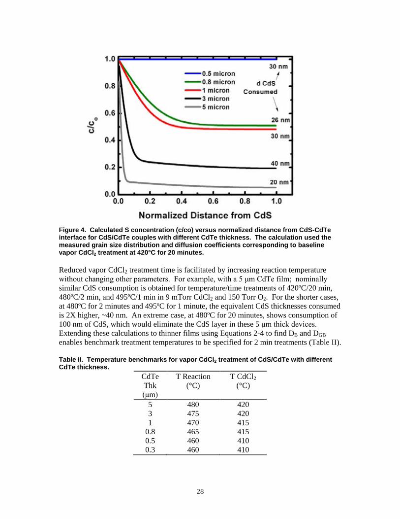
28
Figure 4. Calculated S concentration (c/co) versus normalized distance from CdS-CdTe interface for CdS/CdTe couples with different CdTe thickness. The calculation used the measured grain size distribution and diffusion coefficients corresponding to baseline vapor CdCl2 treatment at 420°C for 20 minutes. Reduced vapor CdCl2 treatment time is facilitated by increasing reaction temperature without changing other parameters. For example, with a 5 μm CdTe film; nominally similar CdS consumption is obtained for temperature/time treatments of 420ºC/20 min, 480ºC/2 min, and 495ºC/1 min in 9 mTorr CdCl2 and 150 Torr O2. For the shorter cases, at 480ºC for 2 minutes and 495ºC for 1 minute, the equivalent CdS thicknesses consumed is 2X higher, ~40 nm. An extreme case, at 480ºC for 20 minutes, shows consumption of 100 nm of CdS, which would eliminate the CdS layer in these 5 μm thick devices. Extending these calculations to thinner films using Equations 2-4 to find DB and DGB enables benchmark treatment temperatures to be specified for 2 min treatments (Table II). Table II. Temperature benchmarks for vapor CdCl2 treatment of CdS/CdTe with different CdTe thickness.
CdTe Thk (μm)
T Reaction (°C)
T CdCl2 (°C)
5 480 420 3 475 420 1 470 415
0.8 465 415 0.5 460 410 0.3 460 410
29
The AM1.5 performance of baseline (5 μm thick CdTe) VT CdTe cells fabricated with vapor CdCl2 treatment at 480ºC with CdCl2 time from 1 to 4 min is shown in Table III. The quantum efficiency (QE) at λ = 400 nm provides a quantitative measure of the final CdS film thickness. In the table, the final CdS film thickness decreases progressively with increasing treatment time over the treatment time range. Given that the starting CdS thickness was 90 nm, the quantity of CdS consumed is comparable to that predicted by the diffusion model above for 5 μm thick films. The cell performance data shows that optimal VOC is obtained for 2-4 min treatment while optimal FF is obtained for 1-2 min treatment. Although the CdS thickness was slightly affected by the treatment time, the JSC was not significantly different. Table III. Best-cell J-V results for VT cells with baseline 5 μm CdTe deposited and vapor CdCl2 treatment at 480ºC with different CdCl2 time.
CdCl2 HT
(min)
VOC (mV)
JSC (mA/ cm2)
FF (%)
η (%)
QE @ 400nm
(%)
Final dCdS (nm)
1 783 23.6 66.6 12.3 40 60 2 796 24.3 69.4 13.4 42 58 2 813 23.6 66.2 12.7 44 55
2.5 800 23.3 65.1 12.2 44 55 4 819 24.3 64.6 12.9 50 35
The treatment conditions of Table II were adopted for the fabrication of solar cells with thinner VT CdTe absorber layers. The effect of the BDH etch process was evaluated on samples with different CdTe absorber thickness and 2 min treatment time. A small sample set was sufficient to indicate a dramatic drop in both VOC and FF for cells with absorber thickness <2 μm (Fig 5). The degree of shunting increased as CdTe thickness was reduced, and many cells were shorted completely. The shunt conductance of baseline cells is typically 1 mS-cm2 and increased to >20 mS-cm2 for 1 μm CdTe.

30
Figure 5. VOC (red circles, left axis) and FF (blue squares, right axis) of CdS/CdTe cells processed with 2 min CdCl2 treatment and BDH etch. A milder surface etch using bromine-methanol (BrMeOH) yielded demonstrable improvement in device yield and tolerance to thinner absorber layers. Fig. 6 shows VOC and FF of cells obtained with thin VT CdTe absorbers using the CdCl2 protocols of Table IV with 2 minute treatments and BrMeOH etch. Baseline VOC is retained down to an absorber thickness of 1.5 μm and follows a monotonic falloff thereafter. The best FF obtained with the BrMeOH etch is comparable to that achieved with the BDH etch but drops progressively with reduced CdTe thickness. However, the FF on cells using the BrMeOH etch are not dominated by shunt conductance. The area yield of cells processed with vapor treatment and mild BrMeOH approaches 100%, which verifies the low pinhole density and demonstrates the benign nature of this back contact process.
Figure 6. VOC (red circles, left axis) and FF (blue squares, right axis) of CdS/CdTe cells processed with 2 min CdCl2 treatment and BrMeOH etch.

31
The best cell results obtained for VT cells with thin CdTe absorber layers using 2 min vapor CdCl2 treatment at 480°C and BrMeOH etching are listed in Table IV. The VOC and FF decrease with reduced CdTe thickness, while JSC remains relatively constant, dropping by ~1 mA/cm2 for the cell with 0.8 μm thick CdTe. Table IV. Best-cell J-V results for VT cells with thin CdTe absorber layers using vapor CdCl2 treatment at 480ºC with 2 minute CdCl2 time and etched with BrMeOH.
CdTe Thickness
(μm)
VOC
(mV)
JSC
(mA/cm2)
FF
(%)
η
(%) 3.0 788 23.1 64.0 11.8 1.5 807 23.8 56.8 10.9 1.0 743 23.4 54.8 9.5 0.8 723 22.5 50.5 8.2
Some device sets, however, exhibit lower photocurrent than expected, based on the CdTe absorption data presented in the previous report (for January 2008 of this contract). The raw and normalized quantum efficiency (QE) of cells with thin CdTe are compared to a baseline cell (5 μm) in Figs. 7 and 8, respectively. The normalized data shows a shift in peak response towards the blue and the expected loss in the red. The raw data shows a 2X panchromatic loss not accounted for by decreased absorption, and QE measurements at reverse bias did not significantly improve collection. Thus, while the photo-response profile is attributable to optical absorption, the magnitude is related to photo-carrier collection. This behavior is correlated with the TEC15 glass batch, and more analysis is required to relate the behavior to glass impurities, effectiveness of the HRT layer as a diffusion barrier, and device processing.
Figure 7. Raw QE (0V, light) of CdS/CdTe cells with baseline (top) and thin CdTe absorbers processed with 2 min CdCl2 treatment.

32
Figure 8. Normalized QE of CdS/CdTe cells with baseline (top) and thin CdTe absorbers of Figure 7. Past x-ray diffraction and photoemission spectroscopic analyses of the surface of vapor CdCl2 treated CdTe films showed the total oxide thickness to be <5 nm, suggesting the possibility of eliminating the etch step altogether for samples prepared with brief vapor CdCl2 treatments. Cells with 3-5 μm CdTe fabricated with short vapor CdCl2 treatment and no etch step yielded 12% conversion efficiencies. Flexible CdTe Solar Cell The goal of this sub-task is development of a process to deposit CdTe films in a superstrate configuration onto CdS/ITO window layers using a temporary Al foil substrate. Both low temperature PVD and high temperature VT deposition methods are considered for the CdTe film growth, allowing comparison of the mechanical and chemical robustness of films deposited at low temperature with those deposited at high temperature. The primary structural effect of deposition temperature is on grain size and structure. The PVD technique, with Ts < 400ºC, does not achieve the grain size and low crystallographic defect density found in films deposited at high temperature (Ts > 450ºC). However, the technique imparts the least thermal stress on the thin film and Al foil system. A primary objective of this work is transferring the completed CdTe solar cell onto a polymer substrate, and the key challenges are selection of an appropriate bonding agent/substrate combination for mechanical robustness and low contact resistance and a chemical etchant for removing the Al substrate. Initial efforts were focused on single-sided adhesive Kapton tape and lamination directly onto polymer substrates using a conductive epoxy. On-going work is the fabrication and characterization of devices to determine: 1) the effect of the Al substrate on p-n junction behavior; 2) the effect of Al etching and etching on device operation; and 3) the mechanical effects of different

33
adhesion methods on the durability of the transferred solar cell. Backwall J-V analysis of partially-completed devices will be used to monitor the progress of junction quality through the post-deposition and transfer process. We anticipate future analysis of stress-induced effects on device operation, in view of the fact that cells will undergo stresses related to mechanical deployment and thermal cycling. The mechanical robustness of the CdTe solar cell transferred to a polymer substrate is an open question. Adhesion and mechanical strength will be characterized with respect to deformation caused by bending of the substrate. Adhesion will be quantified by standard tape tests. Mechanical strength of the structure will be determined by the minimum radius at which the on-set of cracking is detected. In this context, the issue of fatigue fracture will be also be evaluated. Figure 9 shows a schematic representation of the transfer process of a CdTe/CdS thin-film device from the temporary Al superstrate to a flexible polymer substrate. The process steps used in preliminary experiments are: 1. Sputter 0.25-0.30 μm thick ITO film on 0.002 cm thick Al foil; 2. Evaporate 0.2 μm thick CdS film at 220ºC and 3 Å/s; 3. Evaporate 4.0 μm thick CdTe film at 340ºC and 30 Å/s; 4. Vapor treat structure in CdCl2:Ar:O2 ambient at 400ºC for 20 minutes; 5. Vapor treat back surface and deposit Cu to form cuprous telluride; 6. Evaporate Ni contact; 7. Bond cell to polymer substrate; 8. Etch Al foil in 1 molar NaOH at 35ºC.
Ni
CdTe
CdSITO
Al Figure 9a. As-deposited CdTe/CdS superstrate structure on Al foil.

34
Ni
CdTe
CdS
ITOAl
Figure 9b. Intermediate structure bonded to polymer material.
Ni
CdTe
CdS
ITO
Figure 9c. Final CdTe/CdS device: Al foil temporary substrate etched away. To support the Al foil throughout the deposition sequence, it was wrapped around a 10 cm x 10 cm stainless steel platen. Initially, soda lime glass was employed but was found to frequently crack during VT CdTe deposition or during cool-down. In all experiments, the CdS was deposited by PVD at 150°C at a growth rate of 5A/s. Figure 10 shows a photograph of the CdS-coated ITO/Al structure of 1" x 3" sections taken from a PVD and a VT run, each with nominally 4 μm thick CdTe.
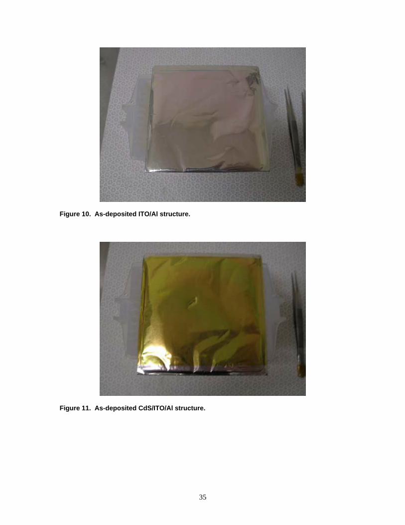
35
Figure 10. As-deposited ITO/Al structure.
Figure 11. As-deposited CdS/ITO/Al structure.

36
Figure 12. CdTe/CdS/ITO/Al structures with CdTe deposited by PVD (left) and VT (right). In a preliminary experiment, we transferred a completed 2 cm x 2 cm Ni/CdTe/CdS/ITO device with a 4 μm thick VT CdTe layer from an Al foil superstrate to Mo-coated Upilex polyimide sheet using a conductive silver epoxy. The temporary foil substrate used was 40 μm thick ultra-high vacuum Al foil supplied by All-Foils, Inc. and the epoxy was No. 40-3905RSI04 by Epoxies Etc. Prior to bonding to Upilex, the cell structure was subjected to the same processing conditions used to fabricate baseline 11% efficient (AM 1.5) solar cells. As neither gridding nor TCO area definition was used in the preliminary experiments, photoresponse measurements were made using point contacts. The structure is flexible, exhibits an open circuit photovoltage of 300 mV and exhibits a weak photocurrent. Cracks in the CdTe film were correlated with crease-like distortions in the Al foil superstrate. Techniques for handling the foil will need to be developed and analyzed to determine the influence of superstrate condition on mechanical integrity of the CdTe film.
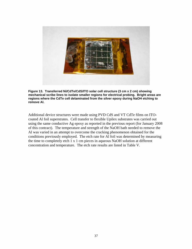
37
Figure 13. Transferred Ni/CdTe/CdS/ITO solar cell structure (3 cm x 2 cm) showing mechanical scribe lines to isolate smaller regions for electrical probing. Bright areas are regions where the CdTe cell delaminated from the silver epoxy during NaOH etching to remove Al. Additional device structures were made using PVD CdS and VT CdTe films on ITO-coated Al foil superstrates. Cell transfer to flexible Upilex substrates was carried out using the same conductive Ag epoxy as reported in the previous report (for January 2008 of this contract). The temperature and strength of the NaOH bath needed to remove the Al was varied in an attempt to overcome the cracking phenomenon obtained for the conditions previously employed. The etch rate for Al foil was determined by measuring the time to completely etch 1 x 1 cm pieces in aqueous NaOH solution at different concentration and temperature. The etch rate results are listed in Table V.

38
Table V. Al foil etch rate for different NaOH solution concentration and temperature.
NaOH:H2O Strength (Molar) Temp (ºC)
± 1º C 0.1 0.5 1
Etch rate (μm/min)
30 0.29 0.73 0.85
40 0.45 1.50 1.86
50 0.74 1.85 2.48
60 1.26 3.79 4.97
Experiments with actual device structures were carried out at two extreme points in Table V: 0.1 Mol/30°C and 1 Mol/60°C. At 60°C, significant bubble formation at the edges caused undercutting of the device at the Ni/Ag epoxy interface, even after application of Kapton tape edge sealant. In addition, the Mo was damaged at the Mo/Upilex interface as a result of etching at regions of residual stress and oxidation (Mo grain surfaces), as a consequence of the Mo deposition conditions needed to deposit adherent Mo films on polyimide. At 30°C, the etch time was excessively long, and the entire structure was immersed in the bath for nearly an hour. In both cases, the transferred devices exhibit no detectable photoresponse. On-going effort is directed at evaluating alternative adhesives and mechanically robust and chemically inert back contact materials and configurations. In practice, transfer of PVD films was more robust then VT films. Backwall VOC measurements after CdCl2 treatment but prior to transfer gave VOC > 700mV for both sample types. After transfer and removal of Al, VOC < 400mV was obtained. The results indicate that more work is needed to address mechanical and chemical issues of the transfer and that deposition of the cell onto Al superstrates does not degrade cell performance. 2.8 References 1G. M Hanket, B. E. McCandless, W. A. Buchanan, S. Fields, R. W. Birkmire, “Design of a vapor transport deposition process for thin film materials,” J. Vac. Sci. Tech. A 24(5), (2006), 1695. 2B. E. McCandless, H. Hichri, G. Hanket, R. W. Birkmire, “Vapor phase treatment of CdTe/CdS thin films with CdCl2:O2,” Proc. 25th IEEE PVSC, (1996), 781.
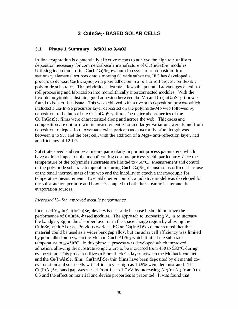
39
3 CuInSe2- BASED SOLAR CELLS
3.1 Phase 1 Summary: 9/5/01 to 9/4/02 In-line evaporation is a potentially effective means to achieve the high rate uniform deposition necessary for commercial-scale manufacture of Cu(InGa)Se2 modules. Utilizing its unique in-line Cu(InGa)Se2 evaporation system for deposition from stationary elemental sources onto a moving 6” wide substrate, IEC has developed a process to deposit Cu(InGa)Se2 with good adhesion in a roll-to-roll process on flexible polyimide substrates. The polyimide substrate allows the potential advantages of roll-to-roll processing and fabrication into monolithically interconnected modules. With the flexible polyimide substrate, good adhesion between the Mo and Cu(InGa)Se2 film was found to be a critical issue. This was achieved with a two step deposition process which included a Ga-In-Se precursor layer deposited on the polyimide/Mo web followed by deposition of the bulk of the Cu(InGa)Se2 film. The materials properties of the Cu(InGa)Se2 films were characterized along and across the web. Thickness and composition are uniform within measurement error and larger variations were found from deposition to deposition. Average device performance over a five-foot length was between 8 to 9% and the best cell, with the addition of a MgF2 anti-reflection layer, had an efficiency of 12.1% Substrate speed and temperature are particularly important process parameters, which have a direct impact on the manufacturing cost and process yield, particularly since the temperature of the polyimide substrates are limited to 450°C. Measurement and control of the polyimide substrate temperature during Cu(InGa)Se2 deposition is difficult because of the small thermal mass of the web and the inability to attach a thermocouple for temperature measurement. To enable better control, a radiative model was developed for the substrate temperature and how it is coupled to both the substrate heater and the evaporation sources. Increased Voc for improved module performance Increased Voc in Cu(InGa)Se2 devices is desirable because it should improve the performance of CuInSe2-based modules. The approach to increasing Voc is to increase the bandgap, Eg, in the absorber layer or in the space charge region by alloying the CuInSe2 with Al or S. Previous work at IEC on Cu(InAl)Se2 demonstrated that this material could be used as a wider bandgap alloy, but the solar cell efficiency was limited by poor adhesion between the Mo and Cu(InAl)Se2 which limited the substrate temperature to ≤ 450°C. In this phase, a process was developed which improved adhesion, allowing the substrate temperature to be increased from 450 to 530°C during evaporation. This process utilizes a 5 nm thick Ga layer between the Mo back contact and the Cu(InAl)Se2 film. Cu(InAl)Se2 thin films have been deposited by elemental co-evaporation and solar cells with efficiency as high as 16.9% were demonstrated. The Cu(InAl)Se2 band gap was varied from 1.1 to 1.7 eV by increasing Al/(In+Al) from 0 to 0.5 and the effect on material and device properties is presented. It was found that

40
Cu(InAl)Se2 cells with band gaps greater than 1.5 eV have comparable efficiencies to the best cells using other wide band gap chalcopyrite alloys. The effects of the increase in substrate temperature on the films and devices were also characterized. The partial replacement of Se with S in the surface region of Cu(InGa)Se2 films can also be used to increase Voc. Optimization of this effect requires a quantitative understanding of the S incorporation process into the absorber layer. In thin films both bulk and grain boundary diffusion must be considered. For S reaction with CuInSe2 films that are slightly Cu rich, a model assuming constant diffusion coefficients has been previously developed. In sulfurization experiments on films, which were slightly Cu deficient, smaller values of the diffusion coefficient, were found and could not be analyzed by the simple diffusion model. The results suggested that the diffusion coefficient could be concentration dependent. Experiments to separate the effects of the bulk and grain boundary diffusion and of a second Cu-Se phase are currently being developed.
Atomic level surface and interface characterization A more fundamental understanding of Cu(InGa)Se2 solar cells will require characterization of the critical surfaces and interfaces in the devices. IEC has begun to address some of the issues related to surfaces and interfaces using atomic level surface characterization and device characterization techniques. In this phase, effort has focussed on two areas. The first has been to develop the capability to deposit ZnS and CdZnS buffer layers using chemical bath deposition methods. This will be used to study the effect of the Cu(InGa)Se2/buffer layer interface chemistry and band alignment on devices. A process for chemical bath deposition of ZnS from solutions of ZnSO4, thiourea and ammonia was developed. The bath conditions and concentrations were optimized to deposit homogeneous microcrystalline films with 3.6 eV bandgap and good coverage on all substrates. Cu(InGa)Se2 solar cells fabricated with the ZnS buffer had higher quantum efficiency at short wavelengths but Voc and FF were a little lower than those with CdS buffer. The best cell with the ZnS buffer had 13.9% efficiency. CdZnS films have also been deposited by chemical bath deposition. Comparable cell performance was obtained with CdS or CdZnS. The second area of focus has been Cu(InGa)Se2 surface characterization to quantitatively analyze the accumulation of Na on the surface and diffusion from the glass substrate. The Na diffusion was found to depend on the atmosphere in which samples were annealed, with Na accumulating on the Cu(InGa)Se2 surface after anneals in O2 or air, but not in vacuum. Also the Na accumulation depended on the previous history of the sample with the surface concentration decreasing after successive cycles of cleaning the surface and annealing. Finally, the apparent activation energy for Na diffusion through the Mo and Cu(InGa)Se2 was determined from the surface concentrations after anneals at different temperatures.

41
Cu(InGa)Se2 TFP Team Activity and Collaboration IEC fabricated complete solar cells and completed JV and QE measurements and analysis on a set of absorber layers provided by 5 different members of the Absorber Sub-team for the CIS Team of the Thin Film PV Partnership. This set included 3-4 samples each from EPV, GSE, ISET, NREL, and SSI. Details and results are presented in the National CIS R&D Team Minutes of the meeting at New Orleans on May 19, 2002.
3.2 Phase 2 Summary: 9/5/02 to 9/4/03 Development of the roll-to-roll deposition of CIGS on polyimide web focused on film cracking and / low adhesion with specific effort on finding a correlation with the Mo deposition process. Mo films were deposited onto two types of Upilex (S and SG) with and without oxygen plasma treatment and at different temperatures and gas pressures but CIGS film cracking and adhesion were found to be insensitive to these variations. A number of changes were made to the CIGS roll-to-roll deposition system to improve its robustness and reproductibility. In this respect, a new Se source design now allows the control of the surface temperature of the liquid Se source. Shielding of the thermocouple extension wires made possible the temperature control of the source effusion rates, which is more robust than the Atomic Absorption Spectroscopy control. Work on CIS-based devices with increased VOC focused on adhesion and material and device performance of Al containing alloys, and on S diffusion into CIS and CIGS films. Al alloy films have been deposited by 1-step (constant flux), 2-step (Al-rich flux followed by Cu-free flux), and 3-step (Cu-free flux at low temperatures followed by only Cu flux and then Cu-free flux at higher temperatures processes. Going from 1-step to 3-step processes grain size was found to increase. Film adhesion was similar for 1-step and 2-step processes, but much worse for the films prepared by the 3-step process. Device results showed similar efficiencies for 1-step and 2-step processes, decreasing with increasing Al content. Films prepared by the 3-step process could not be made into devices except for the lowest Al content films due to the poor adhesion. QE data showed increasing voltage dependent collection with increasing Al content, i.e. increasing bandgap. Characterization of the physical vapor deposited films on Cu, Al and Se to form the ternary CuAlSe2 showed different structure depending on the ratio of Se flux RSE to total metal flux RM. RSE/RM <10 gives mixed phases of Cu-Al inter-metallic phases plus Al2Se3 to CuAlSe2 + Cu2Se going through single-phase CuAlSe2 depending on the Cu/Al ratio. For RSE/RM >10 the structure is a mixture of CuAlSe2 and a new phase β-CuAlSe2. In the area of fundamental studies, alternative emitter layer materials and processes were evaluated and optical properties and electronic transitions in Cu(InGa)Se2 films were determined through spectroscopic ellipsometry. Air annealed chemical bath deposited ZnS films to form mixed sulfide-oxide layers were characterized both optically and structurally. While bandgap decreases with air anneal intensity, glancing angle incidence

42
XRD does not indicate any sulfide-oxide alloy formation. Devices made with the ZnS window layer do not show any correlation between efficiency and air-anneal time. CdS layers formed by chemical surface deposition method were evaluated for their potential in Cu(InGa)Se2 based devices. The process is highly desirable from a manufacturing point of view, since it has high utilization rate and low waste; devices made with CdS deposited by this process demonstrated high efficiencies showing the expected promise. Optical constants of polycrystalline thin film CuIn1-xGaxSe2 alloys with Ga/(Ga+In) ratios from 0 to 1 have been determined by spectroscopic ellipsometry over an energy range from 0.75 to 4.6eV. CuIn1-xGaxSe2 films were deposited by simultaneous thermal evaporation of elemental copper, indium, gallium and selenium. X-ray diffraction measurements show that the CuIn1-xGaxSe2 films are single phase. Due to their high surface roughness, the films are generally not suitable for ellipsometer measurements. An innovative method was developed in which spectroscopic ellipsometer measurements were carried out on the reverse side of the CuIn1-xGaxSe2 Films immediately after peeling them from the Mo-coated soda lime glass substrates. A detailed description of multilayer optical modeling of ellipsometric data, generic to ternary chalcopyrite films, is presented. Accurate values of the refractive index and extinction coefficient were obtained and the effects of varying Ga concentration on the electronic transition were determined.
CIGS TFP Team Activity and Collaboration
IEC attended the National CIS R&D Team meeting on January 30-31, 2003 and participated in work by the Absorber Sub-team. We presented a review titled “Status of Wide Bandgap CuInSe2-based Solar Cells”. Additional team-related activity and collaboration included: • Cu(InGa)Se2 samples deposited at either 400°C or 550°C using either a uniform or bi-
layer (Cu-rich at start) deposition process were provided to the University of Illinois for TEM characterization. A set of well characterized Cu(InGa)Se2 films were also provided to UI for EDS standards.
• IEC fabricated devices on a set of 12 Cu(InGa)S2 films from Florida Solar Energy
Center and completed J-V and QE measurements to assist FSEC in evaluating it’s absorber layer and device fabrication processes.
• Optical constants measured by spectroscopic ellipsometry as a function of energy of
Cu(InGa)Se2 with different relative Ga content were sent to several team members for input into their modeling efforts.
• CdS and ZnO/ITO depositions were completed on several sets of samples, in a round-
robin experiment with GSE and NREL, to use for characterization of GSE’s device processing and calibration of their emitter and TCO layer thicknesses.
43
• Collaboration with the University of Oregon on device characterization continued with focus on Cu(InAl)Se2 devices with different bandgaps for comparison to previously characterized Cu(InGa)Se2 devices.
3.3 Phase 3 Summary: 9/5/03 to 9/4/04 The process for the roll-to-roll deposition of Cu(InGa)Se2 on polymer substrate has been improved during the past year by developing several system improvements and reducing or eliminating the cracking of the Mo back contact film in the Cu(InGa)Se2 reactor. The system was made more robust and stable with a new evaporation source design and improved Se delivery system. The new Cu source has a design, which avoids sharp internal lines and corners that acted as stress concentrators. In addition, the design includes conical nozzles that eliminated spitting of Cu droplets and allows higher rate deposition. The Se delivery manifold was simplified and reduced to a single 3/8" stainless steel tube with two effusion holes. A larger Se source was designed and implemented which incorporates improved ability to measure and control the melt temperature as well as greater capacity. Cracking of the Mo film on polyimide substrates after Cu(InGa)Se2 deposition has been a significant problem hampering progress with the roll-to-roll flexible Cu(InGa)Se2. The extent of film cracking was reduced with lower excess Se flux in the reactor implying that reaction of the Mo back-contact with Se was responsible for crack formation by reducing the yield strength of the Mo film. Since Mo oxides are more stable than the selenides, Mo films were prepared containing around 8 at% oxygen by sputtering in a mixed Ar/O2 atmosphere. It was thought that introducing controlled oxygen content into the Mo film could reduce reaction with Se and thus eliminate cracking. Based on this line of logic. These films did not show any cracks, as evidenced by microscopic characterization and by device performance, indicating that the oxygenated Mo had reduced reaction with Se to prevent cracking. With these changes to the system and substrate, improved deposition reproducibility and compositional and device uniformity was demonstrated. Diffusion of sulfur into Cu(InGa)Se2 thin films could provide a means to increase VOC by widening the bandgap in the space charge region of the absorber. A fundamental study of the mechanisms of S-diffusion was completed using reaction of thin films and crystals in H2S. Two modes of S incorporation in the CuInSe2 were distinguished. Rapid S incorporation with a breakdown of the crystal lattice occurred in materials containing excess Cu. In single-phase films or crystals, a slow S incorporation was observed. Quantitative models of the S-diffusion and diffusion coefficients were developed for these two cases. Also, S was incorporated into evaporated CuInSe2 and Cu(InGa)Se2 films by annealing them in diluted hydrogen sulfide combined with oxygen and hydrogen selenide. After reaction in H2S or H2S combined with O2, a fully converted sulfide layer was formed at the surface of the absorber layer, which would create a barrier for current collection in devices. A mixed hydride gas H2S + H2Se a graded Cu(InGa)(SeS)2 layer on the top of the absorber layer was formed and at the same time the Ga diffuses away from the surface. Thus, the bandgap in the near surface region could not be controllably
44
increased with S diffusion so it does not appear to be a promising avenue for increased VOC. Research on CuInSe2-based devices with increased VOC has focused on determining the cause for poor adhesion which has limited the ability to fabricate wide bandgap Cu(InAl)Se2 devices, and on S-diffusion in Cu(InGa)Se2 for widening the bandgap in the near surface region. Poor adhesion at the Mo/Cu(InAl)Se2 interface was identified as a critical issue and was previously improved by incorporating a thin, ~ 5 nm, Ga layer sputtered onto the Mo film prior to the Cu(InAl)Se2 deposition. Still, devices with increasing bandgap or using different deposition processes were severely hampered by poor Mo/Cu(InAl)Se2 adhesion. Poor adhesion at the Mo interface can also be problematic for the fabrication of Cu(InGa)Se2 cells on flexible polyimide substrates. Research is focused on determining how Ga and/or Al at the Mo interface affects the formation and orientation of a MoSe2 interlayer. The MoSe2 forms a layered structure and orientation of these layers parallel to the substrate can lead to poor adhesion. Mo, Mo/Cu and Mo/Ga layers were reacted with Se and x-ray diffraction measurements showed that the MoSe2 had a more preferred orientation with Ga than with Cu. Similar experiments with Al could not be completed since it was limited by the formation of Al2O3 or, with Mo/Cu/Al layers, formation of Cu-Al intermetallic compounds. A second method was to characterize the MoSe2 after peeling off the CuInSe2-based films but the remaining layers were found to be unstable. Fundamental characterization of the optical properties of Cu(InGa)Se2 continued. Previously, a method to determine optical constants of Cu(InGa)Se2 films using spectroscopic ellipsometry (SE) was developed and variation with Ga/(Ga+In) ratios from 0 to 1 was determined. In this phase, we have focused on the effect of Cu stoichiometry in Cu-poor materials since high efficiency devices are made using single or two-phase Cu-poor films. For both Cu-In-Se and Cu-In-Ga-Se alloy films, an optical model was developed which allows the optical constants of mixed phase materials to be described by a mixture of the single phases, CuInSe2 and CuIn3Se5 for the ternary case. Complete determination of the optical constants for films with Cu at. % from 11 to 25 % was completed. This enables the composition of the mixed phase materials to be determined using the SE measurements. For each alloy system, there is an increase in the energy of the lowest order transitions, which determine the bandgap. Also, there is a broadening of critical point feature, which indicated decreasing crystalline quality. The effect of the Cu(InGa)Se2/emitter layer interface and band alignment on devices is being studied by changing the alloy compositions of the Cu(InGa)Se2 layers and using CdS, (CdZn)S or ZnS emitter layers. Also, chemical bath (CBD) and high utilization chemical surface (CSD) depositions were compared. A process for CSD (CdZn)S was developed and increased bandgap with Zn addition was confirmed by QE measurements. In all cases, the (CdZn)S gave comparable performance to the CdS emitter layer with both 1.2 and 1.4 – 1.5 eV absorber layer bandgaps. The ZnS emitter layers gave poor device efficiency. The CSD process resulted in ~30 mV lower VOC than the CBD process which was not improved with an ammonia surface treatment prior to CdS
45
deposition similar to the first step in the CBD process, indicating the complexity of the interface chemistry in controlling device behavior.
Cu(InGa)Se2 TFP Team activities and collaboration IEC activities in support of the CuInSe2 National Team and other research groups working on CuInSe2 development have included the following: Thin Film Partnership CuInSe2 National Team: IEC has collaborated with several members of the Absorber Sub-Team to complete a study comparing characterization of films and devices from 6 different groups. In particular, IEC completed analysis of J-V and QE data on devices it had previously fabricated using different Cu(InGa)(SeS)2 absorber layers. University of Illinois: Cu(InGa)Se2 samples were provided to the U. of Illinois for TEM and other microstructural analysis. Specific samples included films deposited at different temperatures, comparing uniform flux, two-step, and three-step processes, and deposited on Na-free glass for comparison to films grown with Na diffusion from the soda lime glass substrate. University of Oregon: IEC continued its collaboration with the University of Oregon in the analysis of Cu(InGa)Se2 based devices. Specifically, IEC has provided various devices using different absorber layers and substrates. Miasole: IEC fabricated solar cells and completed JV and QE measurements to help Miasole characterize their Cu(InGa)Se2 deposition process. InterPhases Research: IEC completed cell fabrication and provided J-V testing on a set of samples from InterPhases Research to test their novel surface treatments. In addition, IEC has provided glass/Mo/Cu(InGa)Se2 films for treatment
3.4 Phase 4 Summary: 9/5/04 to 9/4/05 Research on CuInSe2-based solar cells includes four different tasks: (1) In-Line Evaporation; (2) Wide Bandgap Materials; (3) Cu(InGa)(SeS)2 Formation by H2Se/H2S Reaction; and (4) Fundamental Materials and Interface Characterization. In each case, significant progress has been made, as documented in this report. The development of the process of in-line deposition of Cu(InGa)Se2 on polymer substrates focused on the linear metal evaporation sources and on the preliminary investigation on the understanding of the role of oxygen in Mo back contact in preventing film cracking. The insulation of the 6" metal sources that are presently in use has been entirely modified, switching over to rigid alumina boards. In parallel with this change, all the carbon/graphite-based components in the source have been replaced to eliminate
46
reaction with metallic parts, such as thermocouples and Ta shields. These changes enabled operation of the sources at lower temperatures. The problem of metal vapors leaking between the lid and the source body was also addressed. A sealed source was designed and fabricated. This new source will be tested in the near future. The instability of the Cu source power control at high temperature was finally traced to the multi-channel thermocouple interface module which generated a noisy signal for C-type thermocouple when the signal gets to be higher than 20mV and that there are other thermocouples connected to other channels. The temporary solution, connecting the Cu source thermocouple to its own interface module, allowed system operation without any control problem. In addition, issues associated with the sources in scaling-up the in-line deposition to 13" web were investigated. A bell-jar system with a single source was set-up to determine and analyze the temperature distribution on the present 6" source. Further, simulation of the temperature distribution on a 13" system was performed. The comparison showed that simple scale-up of present sources, which give adequate film uniformity, would result unacceptable non-uniformities over the 13" wide web. Consequently, a number of design options to overcome this problem were evaluated. The issues related to source depletion over long runs, resulting in thermal characteristics leading to drifts in the effusion rates, were also examined. As to the role of oxygen in preventing the Mo back contact film cracking, the Auger depth profiling analysis shed more light to the problem. Comparison of the profiles before and after the Cu(InGa)Se2 deposition showed that there is a diffusional rearrangement of oxygen in the Mo layer, resulting in a uniform distribution, irrespective of the initial oxygen distribution in the Mo film. This point will be further pursued in the coming year. Work on wide bandgap materials remained focused on Cu(InAl)Se2 films deposited by multisource elemental co-evaporation. The primary problems being addressed are poor reproducibility, partly caused by poor adhesion at the Mo/Cu(InAl)Se2 interface, and poor performance with low Voc as the bandgap is increased. Progress is reported in this report on developing alternative evaporation sequences, characterizing the back contact, and gaining a more complete understanding of the basic material properties. A simplified continuous version of a three-stage evaporation process was developed and end-point detection of the substrate temperature was used to control the film composition. Films were grown with different relative Al contents material. As Al content increased, the grain size decreased, adhesion worsened, and device performance got much worse. The variation in material and device properties as a function of Cu off-stoichiometry was also studied. Formation of an ordered vacancy chalcopyrite structure with low Cu content was verified. Devices with this compound had poor device performance and an ~ 0.2 eV shift in the long-wavelength QE, indicating a shift in bandgap. Critical issues for the formation of Cu(InGa)(SeS)2 films by the selenization or sulfization reactions of Cu-Ga-In precursor films have been investigated. A complete understanding of the reaction process requires characterizing phases in the as-deposited precursor films, and after annealing with different time-temperature-gas concentration profiles used to control the reaction pathway. Metal precursor films were deposited by sputtering a Cu-Ga layer from a Cu0.8Ga0.2 alloy target, followed by an In layer. The phases present in the sputtered metal precursors after annealing at 450°C were Cu, In,
47
CuIn and Cu9(In1-xGax)4. Films reacted in hydrogen selenide (H2Se) or hydrogen sulfide (H2S) were characterized and unreacted intermetallic Cu-Ga or Cu-In phases respectively were identified at the back of the films. This indicates a reaction preference of Se with In, and S with Ga. Homogenization of the Ga using a two-step selenization/sulfization process that takes advantage of this reaction preference was confirmed, and different time-temperature profiles were compared. Devices with Voc > 0.64 V and eff. > 13% were demonstrated. With a better understanding of the reaction pathway, work will be focused on optimization of the time-temperature sequence of the two-step reaction to better understand the mechanism for Ga mobility to control the S composition at the front of the film, and ultimately, to improve device performance. Fundamental characterization of materials and interfaces has largely focused on a detailed characterization of the optical properties of Cu(InGa)Se2 thin films as a function of changes in composition, including variations in the relative gallium and copper concentrations. The characterization was done using variable angle spectroscopic ellipsometry with a novel technique developed previously at IEC, in which the Cu(InGa)Se2 is lifted off the glass/Mo substrate to provide access to a smooth surface for optical characterization. The complex optical constants and critical transition energies of Cu(InGa)Se2 were previously determined for films varying in relative gallium content spanning from CuInSe2 to CuGaSe2. Since all Cu(InGa)Se2 solar cells are made using Cu-deficient films, it is valuable to relate the optical properties to the degree of Cu off-stoichiometry. A method has been developed to determine the optical constants of films with decreasing Cu content in the Cu-deficient two-phase region as a mixture of the optical properties of the single-phase endpoints with high and low Cu concentrations. The decrease in Cu is characterized by an increase in the fundamental bandgap and broadening of critical point features in the optical constants suggesting degradation of the crystalline quality of the material. This optical analysis can be used to determine the volume fraction of these two phases, which directly determines the film composition. An aqueous Br-etch has been used for smoothing Cu(InGa)Se2 films to obtain a specular surface for optical modeling and interface characterization. The etch also controllably reduces the Cu(InGa)Se2 thickness to study device behavior with thin absorbers and enable characterization of the Mo/Cu(InGa)Se2 interface. The etch procedure was optimized to give the smoothest surface and controllable etch rates. Determination of Cu(InGa)Se2 optical constants using the etch surface or the smooth surface obtained by peeling the films from the Mo contact gave comparable results so the etch does not seem not change the bulk Cu(InGa)Se2. Devices fabricated after etching for different times had lower Jsc due to increased reflectivity with the specular surface and a lower Voc that is not understood. Further efforts will be used to characterize the effects of Cu(InGa)Se2 thickness and the back contact. Research has also focused on the Cu(InGa)Se2/CdS interface. High utilization chemical surface deposition was compared to chemical bath deposition, and it was shown that, under well controlled conditions, the same average device performance could be obtained. Also, optical constants of the CdS grown by chemical bath deposition were

48
measured directly on Cu(InGa)Se2, using ellipsometry and showed broad optical transition consistent with poor crystallinity.
Cu(InGa)Se2 TFP Team Activity and Collaboration IEC activities in support of the CuInSe2 National Team and other research groups working on Cu(InGa)Se2 development have included the following: Thin Film Partnership – CuInSe2 National Team IEC attended the CuInSe2 National Team meeting on March 8, 2005 and gave a presentation titled “Cu(InGa)Se2 processing research at IEC: Composition control during selenization.” IEC also continued its ongoing collaboration with team members in the characterization of Cu(InGa)Se2 films and devices from different groups. This work has resulted in the paper: “Comparison of device performance and measured transport parameters in widely-varying Cu(In,Ga)(Se,S)2 solar cells” by I. L. Repins, B. J. Stanbery, D. L. Young, S. S. Li, W. K. Metzger, C. L. Perkins, W. N. Shafarman, M. E. Beck, L. Chen, V. K. Kapur, D. Tarrant, M. D. Gonzalez, D. G. Jensen, T. J. Anderson, X. Wang, L. L. Kerr, B. Keyes, S. Asher, A. Delahoy, B. Von Roedern, published in Progress in Photovoltaics. Energy Photovoltaics IEC has collaborated with EPV on alternative back contacts. In particular, IEC has fabricated and characterized devices using alternative back contacts deposited by EPV, which should provide improved reflectivity for devices with thin Cu(InGa)Se2 absorbers. In addition, IEC has collaborated with EPV on evaporation source design and provided a design for a laboratory scale Cu evaporation source. ISET IEC has assisted ISET in the characterization of series resistance in devices and the design of collection grids for solar cells. In addition, IEC provided Mo-coated polyamide substrates for fabrication of flexible Cu(InGa)Se2 solar cells. University of Illinois IEC has provided samples for novel characterization at University of Illinois This includes structural characterization using high resolution TEM techniques and Near Field Scanning Optical Microscopy (NSOM) measurements. This work has resulted in a paper “Application of Advanced Microstructural and Microchemical Microscopy Techniques to Chalcopyrite Solar Cells,” C. Lei, C.M. Li, A. Rockett, I.M. Robertson and W.N. Shafarman, Mat. Res. Soc. Symp. Proc., (2005) In press. University of Oregon IEC has continued its ongoing collaboration with the U. of Oregon to characterize electronic properties of Cu(InGa)Se2 solar cells. In the past year this has resulted in two publications: “Detailed Study of Metastable Effects in the Cu(InGa)Se2 Alloys: Test of Defect Creation Models,” J.W. Lee, J.T. Heath, J.D. Cohen and W.N. Shafarman, Mat.
49
Res. Soc. Symp. Proc. 865, 373 (2005), and “Defect Studies Using Photocapacitance Spectroscopy in the Copper Indium Diselenide Alloys,” J.D. Cohen, J.T. Heath and W.N. Shafarman, Chapter 13 in Wide Gap Chalcopyrites, ed. by U. Rau S. Siebentritt (Springer Scientific, 2005) In press.
3.5 Phase 5 Summary: 9/5/05 to 3/31/07 Efforts on CuInSe2-based solar cells include work on four different topics: (1) Cu(InGa)(SeS)2 formation by H2Se/H2S reaction; (2) wide bandgap materials; (3) reduced thickness for Cu(InGa)Se2 absorber layers; and (4) characterization of the Mo/Cu(InGa)(SeS)2 contact. The two-reaction selenization/sulfization of metallic Cu-In-Ga precursors is a commercially viable process for the manufacture of Cu(InGa)(SeS)2 films. A two-step process with partial reaction in H2Se followed by higher temperature reaction in H2S has been shown to produce films with controlled incorporation of Ga. This enables higher bandgap in the active region of the film and higher VOC in devices. In this report, results are included in three aspects of the characterization of Cu(InGa)(SeS)2 formation by the reaction of Cu-Ga-In precursors: characterization of the metallic precursor layers; characterization of lateral non-uniformities in the reacted films; and results with the two-step H2Se/H2S reaction for films with homogeneous [Ga]/[In+Ga] profiles. Metal precursor films were deposited by sputtering a Cu-Ga layer from a Cu0.8Ga0.2 alloy target, followed by an In layer or by sequential Cu, Ga, and In layers. The two precursor structures have different intermetallic phases and morphology in the as-deposited state but after annealing at 450°C, they contain the same mixture of a Cu9(In0.64Ga0.36)4 intermetallic phase and In. A frequent occurrence in the Cu(InGa)(SeS)2 formation by 2-step reaction in H2Se/H2S is the development of lateral non-uniformities in the reacted films. These have been reduced by annealing the precursors to homogenize the phase composition prior to hydride reaction and by improving the uniformity of the heating in the reactor. However, non-uniformities near the sample edges remain and may be caused by a non-uniform Na diffusion. To characterize the two-step H2Se/H2S reaction process, a 2 x 2 matrix of reaction times was examined. Samples were selenized for either 15 or 30 minutes at 450ºC, followed by sulfization at 550ºC for either 15 or 30 minutes. Samples partially selenized for 15 minutes exhibited uniform Ga through the depth of the film after H2S reaction, but those more fully reacted in H2Se for 30 minutes exhibited the commonly observed back-contact Ga accumulation after H2S reaction. In all cases, the S is largely accumulated near the front surface.
Work on wide bandgap materials remained focused on Cu(InAl)Se2 films deposited by multisource elemental co-evaporation. Recent efforts on Cu(InAl)Se2 have focused on developing alternative evaporation sequences and a more complete understanding of fundamental material properties.. Variations in the substrate temperature and composition of films deposited with a modified 3-stage process discussed have been used to characterize the properties of the Cu(InAl)Se2 surface. The formation of a

50
Cu(InAl)2Se3.5 ordered vacancy phase (OVC) phase forms as a surface layer, similar to that found at the surface of Cu(InGa)Se2 films. However, there is no apparent effect of this layer on the device performance. The effects of reducing the thickness of the Cu(InGa)Se2 absorber layer below 1 µm have been studied using an aqueous Br-etch to smooth the surface of Cu(InGa)Se2 films and reduce their thickness. Cu(InGa)Se2 films with uniform through-film composition were etched for different times to vary thickness from 1.8 to 0.4 µm. Solar cells were fabricated with the etched films and with films deposited for different times to vary the thickness. Devices had fill factor greater than 74% over the entire range and little loss in VOC, indicating no change in the critical electronic properties of the devices. The main loss in efficiency with thickness less than 1 µm is from lower short circuit current due partly to incomplete optical absorption but greater than predicted by models. Research has also focused on the Mo/Cu(InGa)(SeS)2 interface since the formation of a MoSe2 layer at the back contact between Mo and Cu(InGa)(SeS)2 can be a source of adhesion problems. Experiments have been done to characterize the reaction of Mo with H2Se and H2S to understand the back contact formation in the process of forming Cu(InGa)(SeS)2 with reaction in the hydride gases. Sputtered Mo films on soda lime glass substrates were reacted for 1 hour in flowing H2Se, H2S, or an equal mixture of the two. XRD and XPS measurements show the formation of MoSe2 at the surface of the films reacted in H2Se or mixed gases and MoS2 only for the film reacted in pure H2S even though the heats of formation favor MoS2 over MoSe2. The interface between the Mo and evaporated CuIn(SeS)2 was also characterized by lifting off the chalcopyrite layer. In this case, the interface layer contained much more S than Se, indicating a preference for the reaction of Mo with S.
CIGS TFP Team Activity and Collaboration
IEC has collaborated with, or provided assistance to, several other university and industrial groups working on Cu(InGa)Se2 solar cells in the past year. These include: Ascent Solar, DayStar, HelioVolt, Miasolé, Nanosolar, SoloPower, Solyndra IEC has leveraged its expertise, baseline processes, and characterization facilities to assist these companies in a variety of ways, including: reacting precursor films to form Cu(InGa)(SeS)2 and characterizing the resulting materials. fabricating cells to validate their cell fabrication processes.
51
Case Western Reserve University IEC provided Cu(InGa)Se2 samples with different compositions and deposited on different substrates for TEM analysis. Energy Photovoltaics (EPV) IEC has continued collaboration with EPV on alternative back contacts. A paper partly on this work was presented at the 2005 AVS International Symposium in Boston “TiN and TiO2:Nb thin film preparation using hollow cathode sputtering with application to solar cells” by S.Y. Guo, W.N. Shafarman, and A.E. Delahoy. Purdue University IEC has reacted novel precursor films in H2Se to help Purdue’s effort to develop alternative processes for Cu(InGa)Se2 formation. University of Nevada, Las Vegas IEC has begun collaboration with Clemens Heske at UNLV in a project to study the absorber/back contact interface in terms of its chemical and electronic properties. Specifically, IEC provided 5 samples, including glass/Mo/Cu(InGa)Se2 and glass/Mo/Cu(InGa)(SeS)2. A procedure for packaging the samples with minimum air exposure was developed for shipping these samples. Initial studies will include photoemission and inverse photoemission measurements on the front surface and on both surfaces of the Mo/Cu(InGa)Se2 interface after peeling the film from the substrate. University of Oregon IEC and Oregon continue to collaborate closely to characterize opto-electronic properties of solar cells with Cu(InGa)Se2 as a function of absorber alloy composition, sodium incorporation, and other processing conditions, with IEC providing sample sets with different compositions or substrates for analysis. University of Syracuse IEC has begun collaboration with Eric Schiff at Syracuse to characterize electronic transport properties of Cu(InGa)Se2. A set of 3 Cu(InGa)Se2 device samples was sent and will be characterized by drift-mobility measurements. University of Toledo IEC provided Cu(InGa)Se2 device samples for piezoelectric measurements.
52
3.6 Phase 6 Summary: 4/1/07 to 12/31/07 In the subtask “In-Line Evaporation of Cu(InGa)Se2” the research objective was to determine the limit of deposition time for Cu(InGa)Se2 in-line evaporation in IEC’s roll-to-roll process and the effects of higher speed deposition on device performance. Our approach was to deposit Cu(InGa)Se2 with increasing web translation speed and source effusion rate and characterize the resulting device performance as a function of thickness and growth rate. A second sub-task focused on “Improved Performance with Absorber Thickness < 1 µm.” In this area the objective was to develop methods to increase JSC in devices using absorber layers with thickness 0.3 ≤ d ≤ 1.0 µm. The approach was to develop methods to implement light scattering into Cu(InGa)Se2 devices and determine its potential for increasing JSC. Determine if the higher absorption coefficient in CuInS2 or S-containing alloys can be used to increase JSC with thin absorbers. To further characterize films and devices with submicron Cu(InGa)Se2 thicknesses, films were evaporated using constant deposition rates and varying times to form layers with thicknesses from 0.35 – 3.3 µm. Characterization of the films showed that the grain size decreases significantly as thickness is reduced less than 1 µm. Devices showed a decrease in performance with decreasing thickness attributed primarily to reduced JSC. A device with Cu(InGa)Se2 thickness 0.35 µm had VOC > 0.6 V and FF > 70% but efficiency 7.9% due to the loss in JSC. Thin CuInS2 absorber layers were deposited and compared to results with Cu(InGa)Se2 to determine the effect of the higher absorption coefficient in the S alloy. The films had a similar reduction in grain size with decreasing thickness. The CuInS2 devices had a loss in JSC which was greater than expected from the optical absorption but the relative decreases in JSC and long wavelength QE were less than with comparable thickness Cu(InGa)Se2. To implement light scattering into Cu(InGa)Se2 devices experiments were done to determine if ITO films could be sufficiently textured using a post-deposition etch. It was found that the films could be textured with HCl but efforts to implement this into processing of Cu(InGa)Se2 cells was not successful with either shunting or very low current. A third subtask on CuInSe2-based solar cells has focused on “Increased VOC for Improved Module Performance.” In this effort our objective was to develop processes to increase VOC in Cu(InGa)(SeS)2 solar cells by controlling film growth and composition. This work has focused on controlling the composition of the pentenary Cu(InGa)(SeS)2 in its formation by the reaction of Cu-Ga-In precursors in H2Se and H2S and in elemental co-evaporation to deposit Cu(InGa)(SeS)2. For Cu(InGa)(SeS)2 films formed by 5-source elemental evaporation we have previously determined the effect of changes in [Cu]/[In+Ga] and [Ga]/[In+Ga] on the relative S incorporation at 550°C substrate temperature. In this work, the dependence of the relative Se and S incorporation chalcogen in Cu(InGa)(SeS)2 on the substrate temperature

53
was characterized with various [S]/[Se+S] flux rate ratios of at TSS. The chalcogen incorporation is the same at 450 – 550°C for both Cu-excess and Cu-deficient growth. However, at 300°C the relative [S]/[Se+S] composition changes when films are grown without excess Cu. The chalcogen incorporation is compared to predictions from equilibrium thermodynamics and to an empirical kinetic model. For Cu(InGa)(SeS)2 films formed by the reaction of Cu0.8Ga0.2/In precursors, a sequential H2Se/H2S reaction process has been used to control through-film composition, avoiding the accumulation of Ga at the back of the film which occurs with reaction in only H2Se. The effect of reaction temperature on film formation and compositional uniformity was evaluated in precursors first selenized in H2Se at 450ºC for 15 minutes, then sulfized in H2S for 30 minutes at fixed temperatures over the range 450 to 550ºC. An abrupt increase in the degree of Ga homogenization is observed for samples sulfized at temperatures of ~500ºC and above, along with a more general increase in S incorporation in the film with increasing temperature. Finally, methods are being investigated to control through-film composition in the formation of Cu(InGa)(SeS)2 films by the reaction of metal precursors by incorporating a copper selenide layer in the precursor to circumvent the formation of Cu-Ga-In intermetallic phases. CuSe/Ga/In and Cu2-xSe/Ga/In precursors were formed by combinations of electrodeposition, annealing, and electron beam evaporation of Ga and In and compared to the sputtered Cu0.8Ga0.2/In precursors. The relative Ga distribution through the film was characterized by XRD and EDS measurements and shown to vary with the different precursor structures. Device results suggest that the precursors containing the binary Cu-selenide phases are reacted in less time than the metallic precursors. CIGS TFP Team Activity and Collaboration
IEC has collaborated with, or provided assistance to, several other university of industrial groups working on Cu(InGa)Se2 solar cells in the past year. These include: Ascent Solar, Dow Chemical, HelioVolt, Nanosolar, SoloPower, Solyndra IEC has leveraged its expertise, baseline processes, and characterization facilities to assist these Cu(InGa)Se2
companies in a variety of ways, including:
• reacting precursor films to form Cu(InGa)(SeS)2 and characterizing the resulting
materials. • fabricating cells to validate their cell fabrication processes. • analysis of materials and devices supplied by the companies. • supplying films or devices for comparison to their materials or calibration of their
measurements. Battelle – Pacific Northwest National Laboratory Baseline IEC Cu(InGa)Se2 devices were provided to Larry Olsen for encapsulation and stability studies including damp heat tests.

54
University of Florida IEC prepared samples for studies of reaction chemistry and kinetics to the group of Tim Anderson. Specifically, stacked (Ga-Se)/(Cu-Se) samples along with control samples from the separate Ga-Se and Cu-Se runs were deposited. University of Illinois IEC provided Cu(InGa)Se2 films to the group of Angus Rockett for photoluminescence measurements. These included different films with varying [Cu]/[In+Ga] and [Ga]/[In+Ga] composition ratios. University of Nevada, Las Vegas
Cu(InGa)Se2 and Cu(InGa)(SeS)2 films were sent to the UNVL group of Clemens Heske for IPES/UPES measurements to characterize the electronic structure of the films. These include a wide range of different compositions including systematic variation in [Cu]/[In+Ga], [Ga]/[In+Ga], and [S]/[Se+S]. University of Oregon IEC and Oregon continue to collaborate closely to characterize opto-electronic properties of solar cells with Cu(InGa)Se2 as a function of absorber alloy composition, sodium incorporation, and other processing conditions, with IEC providing sample sets with different compositions or substrates for analysis. In this contract period IEC prepared and sent two sets of samples. The first was a set of Cu(InGa)(SeS)2 devices with fixed [S]/[Se+S] ≈ 0.25 and varying [Ga]/[In+Ga] and the second was a set of devices with soda lime glass and Ti foil substrates to control the Na content.
3.7 Phase 7 Summary: 1/1/08 to 5/31/08 Composition Control for Increased VOC In this task we are investigating processes to increase VOC in Cu(InGa)(SeS)2 solar cells using absorber layers formed by the reaction of precursors in H2Se / H2S which is typically low due to accumulation of Ga at the back of the reacted film. A two-step reaction of Cu-Ga-In precursors with partial reaction in H2Se at 400° – 450°C followed by completion in H2S at 550°C has been used to form Cu(InGa)(SeS)2 films with uniform incorporation of the Ga.1 To provide a basis for improvements in device performance, efforts are being undertaken to improve the IEC H2Se/H2S baseline process to improve reproducibility. Current studies into the effect of sulfization temperature on Ga homogenization have yielded several possible approaches to improve process reproducibility. Cu0.8Ga0.2/In precursor bi-layers were selenized at 450ºC for 15 minutes, followed by sulfization at temperatures ranging from 450° – 550ºC for 30 minutes. Two samples
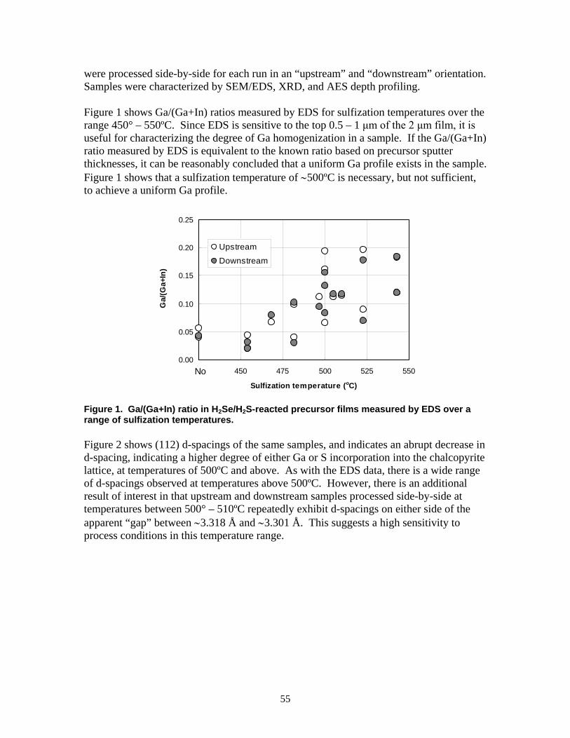
55
were processed side-by-side for each run in an “upstream” and “downstream” orientation. Samples were characterized by SEM/EDS, XRD, and AES depth profiling. Figure 1 shows Ga/(Ga+In) ratios measured by EDS for sulfization temperatures over the range 450° – 550ºC. Since EDS is sensitive to the top 0.5 – 1 μm of the 2 μm film, it is useful for characterizing the degree of Ga homogenization in a sample. If the Ga/(Ga+In) ratio measured by EDS is equivalent to the known ratio based on precursor sputter thicknesses, it can be reasonably concluded that a uniform Ga profile exists in the sample. Figure 1 shows that a sulfization temperature of ∼500ºC is necessary, but not sufficient, to achieve a uniform Ga profile.
0.00
0.05
0.10
0.15
0.20
0.25
425 450 475 500 525 550
Sulfization temperature (oC)
Ga/
(Ga+
In)
Upstream
Downstream
No
Figure 1. Ga/(Ga+In) ratio in H2Se/H2S-reacted precursor films measured by EDS over a range of sulfization temperatures. Figure 2 shows (112) d-spacings of the same samples, and indicates an abrupt decrease in d-spacing, indicating a higher degree of either Ga or S incorporation into the chalcopyrite lattice, at temperatures of 500ºC and above. As with the EDS data, there is a wide range of d-spacings observed at temperatures above 500ºC. However, there is an additional result of interest in that upstream and downstream samples processed side-by-side at temperatures between 500° – 510ºC repeatedly exhibit d-spacings on either side of the apparent “gap” between ∼3.318 Å and ∼3.301 Å. This suggests a high sensitivity to process conditions in this temperature range.

56
3.290
3.300
3.310
3.320
3.330
3.340
3.350
425 450 475 500 525 550
Sulfization temperature (oC)
(112
) d-s
paci
ng (Å
)Upstream
Downstream
No
Figure 2. Chalcopyrite (112) d-spacing for H2Se/H2S-reacted samples over a range of sulfization temperatures. The samples in Figure 1 exhibiting Ga/(Ga+In) < 0.12 at sulfization temperatures exceeding 520ºC, and the samples in Figure 2 exhibiting d > 3.320 in the same temperature range suggest that there are variables in the existing baseline H2Se/H2S process that are not fully understood. It is already known that the degree of selenization influences the degree of Ga homogenization that occurs during sulfization.1,2 It is further known that thermal characteristic times in the existing chalcogenization system are on the order of minutes.3 Therefore, the samples are heating up for a substantial fraction of the 15-minute reaction time. It is therefore suggested that the baseline H2Se/H2S process be modified to utilize a reduced selenization temperature. This will slow down the reaction rate, allowing longer selenization times of which thermal transients represent a much smaller fraction of the reaction time. It is expected that this will result in more reproducible degrees of selenization. Based on the high degree of (112) d-spacing sensitivity during sulfization at temperatures in the range 500° – 510ºC, it is contemplated that the Ga homogenization and sulfization mechanisms may be in competition with one another. It can be inferred that Ga is substantially immobile once is has been incorporated in the chalcopyrite lattice – this is based on the reduced Ga homogenization as degree of selenization increases. As sulfur reacts with Ga-bearing intermetallics, it is driving its incorporation into the chalcopyrite lattice, reducing its mobility. Thus, the homogenization of Ga may be dependent on both temperature and S concentration. A second suggestion for improving the baseline H2Se/H2S process is to incorporate an inert anneal at temperatures between 500° – 550ºC before the introduction of sulfur. This also suggests the possibility of reduced Ga homogenization with increased H2S concentration. This approach has the further benefit making a fundamental determination of whether temperature or sulfur is the driving force for Ga homogenization. It should be noted that Marudachalam found that Ga could be homogenized in fully selenized films by an inert anneal at temperatures above 500ºC.4
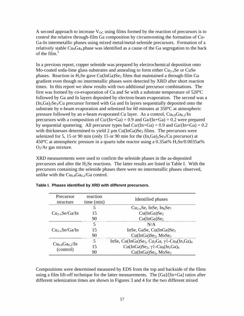
57
A second approach to increase VOC using films formed by the reaction of precursors is to control the relative through-film Ga composition by circumventing the formation of Cu-Ga-In intermetallic phases using mixed metal/metal-selenide precursors. Formation of a relatively stable Cu9Ga4 phase was identified as a cause of the Ga segregation to the back of the film.5 In a previous report, copper selenide was prepared by electrochemical deposition onto Mo-coated soda-lime glass substrates and annealing to form either Cu2-xSe or CuSe phases. Reaction in H2Se gave Cu(InGa)Se2 films that maintained a through-film Ga gradient even though no intermetallic phases were detected by XRD after short reaction times. In this report we show results with two additional precursor combinations. The first was formed by co-evaporation of Cu and Se with a substrate temperature of 520ºC followed by Ga and In layers deposited by electron-beam evaporation. The second was a (In,Ga)2Se3/Cu precursor formed with Ga and In layers sequentially deposited onto the substrate by e-beam evaporation and selenized for 60 minutes at 350ºC at atmospheric pressure followed by an e-beam evaporated Cu layer. As a control, Cu0.8Ga0.2/In precursors with a composition of Cu/(In+Ga) = 0.9 and Ga/(In+Ga) = 0.2 were prepared by sequential sputtering. All precursor types had Cu/(In+Ga) = 0.9 and Ga/(In+Ga) = 0.2 with thicknesses determined to yield 2 µm Cu(InGa)Se2 films. The precursors were selenized for 5, 15 or 90 min (only 15 or 90 min for the (In,Ga)2Se3/Cu precursor) at 450ºC at atmospheric pressure in a quartz tube reactor using a 0.35at% H2Se/0.0035at% O2/Ar gas mixture. XRD measurements were used to confirm the selenide phases in the as-deposited precursors and after the H2Se reactions. The latter results are listed in Table I. With the precursors containing the selenide phases there were no intermetallic phases observed, unlike with the Cu0.8Ga0.2/Ga control. Table I. Phases identified by XRD with different precursors.
Precursor structure
reaction time (min) Identified phases
Cu2-xSe/Ga/In 5 Cu2-xSe, InSe, In6Se7 15 Cu(InGa)Se2 90 Cu(InGa)Se2
Cu2-xSe/Ga/In 5 N/A 15 InSe, GaSe, Cu(InGa)Se2 90 Cu(InGa)Se2, MoSe2
Cu0.8Ga0.2/In (control)
5 InSe, Cu(InGa)Se2, Cu3Ga, γ1-Cu9(In,Ga)4 15 Cu(InGa)Se2, γ1-Cu9(In,Ga)4 90 Cu(InGa)Se2, MoSe2
Compositions were determined measured by EDS from the top and backside of the films using a film lift-off technique for the latter measurements. The [Ga]/[In+Ga] ratios after different selenization times are shown in Figures 3 and 4 for the two different mixed

58
metal/metal-selenide precursors. Both cases showed Ga accumulation at the back of the Cu(InGa)Se2 film, although the Ga gradient may be smaller with the (In,Ga)2Se3/Cu precursor.
Figure 3. [Ga]/[In+Ga] ratios measured by EDS from the top and back sides of Cu2-xSe/Ga/In precursor films selenized for different times. The dashed line shows [Ga]/[In+Ga] in precursor.
Figure 4. [Ga]/[In+Ga] ratios measured by EDS from the top and back sides of (In,Ga)2Se3/Cu precursor films selenized for different times. The dashed line shows [Ga]/[In+Ga] in precursor. Device results of the solar cells made from the precursors following 90 min selenization reactions are shown in Table II. No increase in VOC was obtained with either of the mixed metal/metal-selenide precursors compared to the sputtered metal precursor.

59
Table II. Device J-V parameters of the solar cells made from the selenized precursors.
Precursor VOC (V)
JSC (mA/cm2)
FF (%)
η (%)
Cu2-xSe/Ga/In 0.439 37.2 62.4 10.2 (In,Ga)2Se3/Cu 0.332 32.9 38.1 4.2
control 0.474 36.8 50.5 8.8 In-Line Evaporation Na Incorporation: A NaF effusion source identical to other sources in the system was placed such that it would be 1st source in the direction of travel during the 2nd pass. The shield that forms the deposition zone partially covers effusion from the Na source. The initial Na source temperature was chosen to give an approximate effusion rate of 0.1% that of Cu. Since the sources are geometrically identical this temperature would correspond to NaF vapor pressure equal to 10-3 of the vapor pressure of Cu for the standard operating condition. For the Cu source temperature operating at 1400°C this gives a NaF source temperature of 685°C. Two sets of experiments were performed at the Na source temperature of 685°C. Initially, NaF was turned on during the 1st pass where it was the last source seen by the substrate carrier traveling at 18”/min. Devices made on Upilex substrates did not show any improvements in VOC or FF relative to our baseline. This could be the consequence of high speed substrate travel and low source temperature both of which tend to reduce NaF deposited on the substrate. As a result, a second set of runs were performed keeping the NaF source at the same temperature but moving the evaporation to the 2nd pass when substrate NaF is the 1st source and substrate travel is only 2”/min. Even under these conditions no effect was observed on the devices fabricated on Upilex substrates. The next set of experiments will follow the same protocol except for the NaF temperature which will be increased to give a vapor pressure of 5x10⁻³ that of Cu. Monolithically Integrated Flexible Modules: Scribing tests for monolithic integration by mechanical and laser scribing have been started. Initial attempts in mechanically scribing the molybdenum (Mo) layer (P1 scribe) with a programmable x-y mechanical scribing system resulted in tearing of the Upilex. Double stick tape was then used to secure the Upilex giving much improved results. However, the resulting scribe showed only partial removal of the Mo layer as can be seen in Figure 5 where the optical microscopy image of the mechanical scribe is shown both in reflection and in transmission. Note that even though the back side of the Upilex substrate is coated with 20 nm of Mo it does let enough light go through to have adequate observation in transmission.

60
In the case of scribing the Cu(InGa)Se2 layer (P2 scribe) it was found that even the lightest pressure between the scribe tip and the sample would always remove the Mo from the Upilex. This was in contrast to the films on glass substrates where the P2 scribe left Mo film intact. As a result, the decision was made to test laser scribing for both P1 and P2 scribes.
A
B
Figure 5. Optical microscope image of mechanically scribed Mo on Upilex viewed in reflection (A) and transmission (B).
Initial tests were made with the laser parameters that were successfully used for glass substrates. Figure 6 is the optical micrograph of the P1 scribe performed with the 532 nm laser. In this case, the Mo films were removed completely but there is substantial thermal modification to the Upilex at the center of the scribe.
A
B
Figure 6. Optical microscope image of laser scribed Mo on Upilex viewed in reflection (A) and transmission (B).
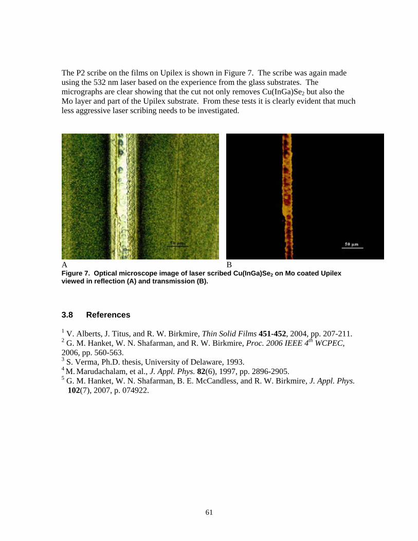
61
The P2 scribe on the films on Upilex is shown in Figure 7. The scribe was again made using the 532 nm laser based on the experience from the glass substrates. The micrographs are clear showing that the cut not only removes Cu(InGa)Se2 but also the Mo layer and part of the Upilex substrate. From these tests it is clearly evident that much less aggressive laser scribing needs to be investigated.
A
B
Figure 7. Optical microscope image of laser scribed Cu(InGa)Se2 on Mo coated Upilex viewed in reflection (A) and transmission (B).
3.8 References 1 V. Alberts, J. Titus, and R. W. Birkmire, Thin Solid Films 451-452, 2004, pp. 207-211. 2 G. M. Hanket, W. N. Shafarman, and R. W. Birkmire, Proc. 2006 IEEE 4th WCPEC, 2006, pp. 560-563. 3 S. Verma, Ph.D. thesis, University of Delaware, 1993. 4 M. Marudachalam, et al., J. Appl. Phys. 82(6), 1997, pp. 2896-2905. 5 G. M. Hanket, W. N. Shafarman, B. E. McCandless, and R. W. Birkmire, J. Appl. Phys.
102(7), 2007, p. 074922.

62
4 Si- BASED SOLAR CELLS
4.1 Phase 1 Summary: 9/5/01 to 9/4/02 During the first year of the program, an in-situ grain enhancement process involving HWCVD Si films deposited on Al-coated glass substrates was evaluated. Two substrate temperatures, 400 and 600 0C, were investigated so as to study conditions below and above the Si-Al eutectic temperature (575 0C). For films deposited at 600 0C, delamination and non-uniform properties were observed. It is believed this was caused by poor wetting characteristics at the Al-glass interface which led to non-uniform Al coverage on the glass substrates. For films deposited at 400 0C, the Si film grain structure, average grain size and crystalline fraction were compared as a function of the growth rate, Si/Al ratio and Si film thickness. In general, the Si film crystalline fraction and average grain size increases with decreasing growth rate, Si/Al ratio and Si film thickness. A maximum average grain size of 100 nm as measured by XRD peak broadening was achieved at 1.0 µm/hr growth rate in a 2.0 µm thick Si sample with a Si/Al ratio of 2. This sample also exhibited a Raman peak profile closely resembling that of bulk c-Si. Further characterization by TEM revealed that the film had a bimodal grain size distribution with regions of nanometer and micron-sized grains. For 5 µm thick Si films, regardless of the growth rates and Si/Al ratios considered, the Si film average grain size and crystalline fraction were 10-50 nm and 75-80%, respectively. This suggests that the growth of micron size crystallites does not continue as the thickness of Si film increases beyond a critical value. At a growth rate of 5 µm/hr, films are similar to those grown on glass with average grain size less than 50 nm and crystalline fraction of ~75%. A series of p-i-n and n-i-p devices were fabricated in order to evaluate the opto-electronic properties of the HWCVD polycrystalline Si i-layers. The devices were fabricated on both n-type and p-type c-Si wafers with the window layers consisting of PECVD n- and p-µc-Si, respectively. Two i-layer thickness values were considered, 2 and 10 µm. In general, all devices showed little rectification in light or dark. The n-i-p’s had Jsc ~2 mA/cm2 and Voc ~30 mV while p-i-n’s showed no photovoltaic behavior. The results from these devices and accompanying n-i-p and p-i-p diagnostic devices lead to the conclusion that the i-layer is highly defective and has significantly short diffusion lengths for both holes and electrons. Devices were also fabricated on small grain µc-Si HWCVD i-layers grown on Al-glass substrates. The structure was glass/µc-Si-Al (HWCVD)/µc-Si i-layer (HWCVD)/µc-Si n-layer (PECVD)/ZnO/grids. The devices were typically shorted. Subsequent analysis has found Al metal penetration to the top of the HWCVD film which could be responsible for the shorting behavior. A study of optical losses and enhancement in a-Si devices on textured SnO2 substrates was undertaken using PVOPTICS, a modeling program developed at NREL by Dr. Bhushan Sopori. Comparison of simulation results with measured photocurrent data obtained from integrating the spectral response at reverse bias with the AM1.5 spectrum in the range of 400-800 nm shows good agreement for a range of devices varying in thickness, texture and back contact reflectivity. The simulations indicated that while the

63
use of textured SnO2 and Al back reflector increase the photocurrent, these gains are partially nullified by equivalent absorption losses in the red region at the front and back contacts. Parasitic losses at the front and back contact occurred for texture angles greater than 10°. Increasing the angle causes better internal trapping in the i-layer, but also higher SnO2/a-Si reflection losses, as well as SnO2 and metal absorption losses. Parasitic absorption in the textured SnO2 due to back reflected light is 1-2 mA/cm2 for typical designs. N-i-p cells have a fundamental advantage over p-i-n cells since the textured TCO is at the rear of the device leading to lower losses. Light trapping in even simplified device structures with textured interfaces can be very complex. The angle of texture can have competing influences which can lead to increases or decreases in JPH depending on other design parameters. Increasing the angle of the texture results in less reflection losses and better light trapping, hence higher photocurrents, but also larger parasitic absorption losses in the SnO2 and metal BR. The original PVOPTICS program had no data files for the optical constants n and k to model SnO2 films. We measured several commercial SnO2 films using our VASE and provided the results to Sopori who incorporated them into a special version of PVOPTICS for IEC use in the above analysis. However, we have been concerned about characterization of VASE on textured surfaces such as SnO2. We carried out VASE measurements on mechanically polished and unpolished Asahi Type U textured SnO2. Polishing significantly reduced but did not eliminate texture. We developed the optical model for the polished film first and then import the textured SnO2 film data in to this optical model. We used a two-layer structure with surface roughness modeled using an effective medium approximation (EMA) layer. For polished films the fit looks excellent. However, for the textured film the fit is not very good, at the higher energy region where the roughness plays a significant role. The depolarization is a strong function of texturing not sample nonuniformity as reported by others. We suspect that this difference is due to the difference in incident angle used between different groups. Our results indicate that the depolarization is caused by the textured surface. Thin Si TFP Team Activity and Collaboration IEC continued providing leadership in the Multijunction Device Team. A presentation was made summarizing the literature on TCO/p contact properties followed by a application of a new method developed at IEC to characterize this contact. It was applied to devices made at IEC on SnO2 and ZnO (from Harvard Univ) and at BP Solar using various interfaces on SnO2 and SnO2/ZnO bilayers. The method was applied to laser scribed minimodules. A key result was that there is no blocking contact or very high resistance between ZnO and p-layers, as is commonly assumed. Instead the diode recombination increased, leading to reduction in Voc and FF.
64
4.2 Phase 2 Summary: 9/5/02 to 9/4/03 The grain size enhancement of HWCVD Si films deposited on Al layers has been investigated in two temperature regimes. These regimes are determined by the eutectic temperature of 575°C in the Si-Al system. With the formation of a liquid phase above the eutectic temperature, a different mechanism is expected to govern the grain enhancement process compared to that expected below this temperature where the Si-Al mixture remains in the solid state. This report describes the results obtained for depositions of HWCVD Si films on Al layers at 430°C and 600°C. Aluminum layers with thickness varying from 0.01 to 1.0 µm were deposited onto Corning 7059 type glass substrates using electron-beam evaporation. Silicon layers were subsequently deposited onto the Al coated samples in the HWCVD system. Silane was used as the source gas with no hydrogen dilution. Silicon layer depositions were carried out at a substrate temperature of 430°C and 600°C, filament temperature of 1850°C and pressure of 25 mTorr. The films were deposited at two different growth rates of 1.0 and 5.0 µm/hr, which were attained by varying the silane flow rate from 4.5 to 22.5 sccm, respectively. Films with thickness values of 2 and 5 µm were deposited with deposition times corresponding to 24 min and 5 hrs, respectively. For deposition at 430°C, Raman spectroscopy and XRD showed Si films deposited on Al had random orientation and higher degree of crystallization compared to films deposited on glass. The crystalline Si Raman profile of films deposited on glass had a typical tail extending toward lower wavenumbers indicative of a-Si and nanocrystalline Si phases. In contrast, films deposited on Al, had profiles similar to those obtained for c-Si. For 2 µm thick films grown at 1 µm/hr, the average grain size and crystalline fraction increases with decreasing Si/Al ratio. The maximum average grain size of 200 nm was achieved with a Si/Al ratio of 2. As the growth rate is increased from 1 to 5 µm/hr, the average grain size and crystalline fraction decreases at a constant Si/Al ratio. AFM analysis revealed that some areas on the film surface are covered with small particles, 10-50 nm in diameter. It is speculated that these features are individual grains, which do not extend throughout the bulk of the Si film. TEM analysis found heterogeneous structure of several large grains but mostly nano-crystalline regions. These two crystalline regions can be found either side by side on the Al layer or as layers with one evolving from the other. It is speculated that the presence of the nano-crystalline phase indicates an incomplete grain enhancement process and that the effect of lower growth rate for given film thickness is to increase the interaction time between the layers. The poly-Si does not form a continuous layer. The bulk of the films also contain Al. Al layer inversion is incomplete, perhaps due to insufficient interaction time between the Si and the Al layer. For 5.0 µm thick samples the average grain size varied between 40 and 70 nm, and the crystalline fraction did not change significantly with the growth rate. The decrease in grain size for Si films with 5 µm thickness may be due to the existence of a limiting thickness beyond which the Al ceases to have an effect on the growth process. If this hypothesis is correct, the film evolves from a large grain to a nanocrystalline grain microstructure as seen on films deposited on glass.
65
Si films deposited at 600°C exhibit larger average grain size as measured by XRD peak broadening. This contrast is more pronounced as the growth rate and Si film thickness increases. However, all films were non-homogeneous in terms of morphology and composition perhaps as a result of poor wetting of the Al layer on the 7059 glass at 600°C or alternatively due to segregation of the liquid phase forming at the eutectic composition. On average, the crystalline volume fraction of films deposited at 600°C is similar to those deposited at 430°C. Fabrication of p-i-n solar cells with all PECVD µc-Si layers was investigated on glass/SnO2 substrates. The 2.0 µm i-layer was deposited for 9 hours. No ZnO or a-Si buffer layers or any other transitional layers were incorporated. Device performance was very poor, with VOC=0.2V and efficiency <1%. CV and QE measurements suggested a relatively high defect density and low barrier height. The µc-Si devices have substantially more absorption below the a-Si absorption edge confirming that their structure is between a-Si and c-Si. Thin film Si n-i-p solar cells were fabricated on n-doped c-Si substrates using PECVD and HWCVD microcrystalline i-layers. No metal induced crystallization was utilized. The structure of the devices was Ag-Pd-Ti/n+-cSi/(PECVD or HWCVD) i-µcSi/PECVD p-µcSi/ITO/Ni-Al. The n+ wafer substrates served as the n-layer in the p-i-n cells. In addition, diagnostic n-p devices were fabricated by depositing PECVD p-µcSi emitter layers directly onto the n+-c-Si substrates. Identical n-i-p and n-p devices were also fabricated which incorporated a 30 nm a-Si buffer layer between the p-layer and i-layer or n+ c-Si. The performance of all solar cell devices was quite poor. All cells with a HW or GD i-layer absorber had less than 1% efficiency although many had well formed diode characteristics in light and dark. Both n-i-p and n+/p+ cells using GD and HW µc-Si absorber i-layers have produced cells with poor photo-carrier collection and high recombination. The a-Si buffer layer increases VOC but reduces JSC and FF in both n-i -p and n+/p+ cells. No first-order differences were seen between devices the HW or GD µc-Si layers. n+/p+ cells with the a-Si buffer achieved VOC=0.62 V but with very poor JSC and FF. Previously, standard a-Si p-i-n devices routinely achieved FF=70% while recently FF has been limited to 50-60%. QE measurements indicated poorhole collection from the i-layer. The most likely cause is donor-like impurities such as P or O, which reduce the lifetime of the hole. Considerable effort was made in cleaning or modifying the PECVD deposition system to eliminate possible sources of O or P. None of these changes resulted in a higher FF. Select samples were sent to NREL for SIMS analysis. Since our PECVD reactor is a single chamber system, a major concern in both a-Si and µc-Si devices is the P and B cross-contamination. Results showed that P and B are quite low in PECVD and HWCVD a-Si films and devices. Some recent devices have had B concentrations of 1018 cm-3 in the p-layer while P was 10 times higher. This suggests our burying layer is not effective anymore in preventing P cross-contamination. Consequently, a new burying procedure is being implemented. For PECVD or HWCVD

66
µc-Si devices, the concentration of O, N and C are several orders of magnitude higher than those in the a-Si cell and the c-Si wafer, as is reported by others. These impurities in the HWCVD samples have a concentration gradient, which decreases from the top surface and level off to a constant bulk concentration at approximately one micron into the film. It is speculated that the lower H content in HWCVD films combined with the excessive number of grain boundaries and film porosity may facilitate contaminant penetration into the films. Boron doped HWCVD films were deposited and characterized. Films were polycrystalline with typical (220) preferred orientation. Crystalline fraction was 75 to 90%. A dependence of conductivity with dopant gas concentration and film thickness was found. For submicron films, conductivies were constant at 10-6 S/cm for B2H6/SiH4 <10-3. At B2H6/SiH4 =10-2, the conductivity reached 10-3 S/cm. For films with thickness > 2 µm and B2H6/SiH4 =10-2, the conductivity further increased to 10-1 S/cm. The effect of thickness on conductivity points to a change in microstructure as the film thickness increases. This hypothesis is corroborated by activation energy data, which indicates a change in mobility with thickness. Future work will include a determination of the effects of film microstructure and dopant gas concentration on film conductivity. Thin Si TFP Team Activity and Collaboration IEC attended the National Thin Film Si Team Meeting held on January 10. 2003 and gave a presentation on the growth and characterization of HWCVD Si films on Al coated glass. We also attended the National Thin Film Si Team Meeting on August 8, 2003 and gave a presentation on the grain enhancement of Si films by aluminum induced crystallization approaches. IEC received 9 plates of a-Si devices from Dr. Gautam Ganguly at BP Solar for measurements and analysis to determine the contact resistance and diode A factor. One series compared textured AFG SnO2 and Harvard ZnO with and without buffer layer deposition before the p-layer. The other series compared different back contact buffer layers. We analyzed the devices as described previously using dark JV measurements on a row of 6 devices per plate to determine the contact resistance, TCO sheet resistance, and diode properties. We found that certain buffer layers significantly decreased the contact resistance. Consistent with results in the above paper, we found that direct deposition onto ZnO leads to much higher A factor ~ 3, not higher contact resistance. The buffer layer allows A to remain ~1.6 as typical of good devices with low contact resistance. This work was subsequently published (Ganguly, Hegedus et al, Appl Physics Lett 85, 2004, 479-481).
4.3 Phase 3 Summary: 9/5/03 to 9/4/04 Post-deposition annealing experiments of Al/Si bi-layers were carried out to compare crystallization and layer inversion processes in standard metal induced crystallization and in-situ metal induced crystallization. Evaporated Si films allowed comparison between films deposited in an H free environment and HWCVD films. First, 0.5 mm thick films

67
of Al were deposited onto 7059 glass substrates by electron beam evaporation. The films were left in ambient air for a period of 24 hr to allow formation of an oxide layer. Si films with 0.6 mm thickness were then deposited by electron beam evaporation and HWCVD. XRD measurements showed no evidence of crystallization of the Si films deposited by evaporation prior to annealing while films deposited by HWCVD were completely crystallized. Annealing was performed for 90 min at 500°C under 100 sccm of Ar. For Si films deposited by evaporation, optical microscopy showed polycrystalline Si nucleation extending to the glass interface with very little lateral grain growth. XRD analysis showed only partial crystallization of these films. For samples with Si films deposited by HWCVD, no increase in grain coalescence or crystalline fraction was observed. Work continued on in-situ crystallization during HWCVD growth. Analysis of HWCVD Si films deposited on Al coated glass substrates below the Si-Al eutectic temperature (~570°C) revealed a layered microstructure. The lower layer near the glass interface is composed of micron size islands of polycrystalline silicon. Atop this layer, a mixture of nanocrystalline Si and Al remains. This mixture is also observed in the spaces between the polycrystalline Si islands. The existence of this layered structure is evidence of layer inversion and is consistent with standard metal induced crystallization results obtained by other groups. However, the discontinuity of the underlying polycrystalline Si structure limits its usefulness for device fabrication. Raman spectroscopy through the glass substrate confirms regions of polycrystalline Si and regions of a mixture of nanocrystalline Si and Al. After etching the overlaying Si-Al mixture, a similar pattern of polycrystalline Si islands is observed from the front surface. Post-deposition anneal at 430 °C under vacuum for 2 hours increased the fractional coverage of c-Si from 60 to 90%. This indicates that the excess Si does not crystallize as it accumulates on the Al layer surface during deposition and is available for further lateral growth of the polycrystalline Si layer. The average grain size appears to decrease with increasing Si/Al ratio and correlates well with the time the Al layers remained exposed to air prior to Si film deposition. The role of aluminum oxides on the layer inversion process and grain size of the polycrystalline Si layer is not well understood. It is hypothesized that the oxide layer acts as a nucleation barrier leading to a lower density of near neighbor nuclei. However, it is expected that the oxide layer is self-limiting and would reach equilibrium after a brief period of time of exposure to air. The present results suggest that the oxide layer continues to change long after deposition. In order to consider the effect of growth rate and Si/Al ratio, Si films with thickness of 2-3 µm was deposited by HWCVD at 5 µm/hr at 430°C on Al layers 100, 250, 500 and 1000 nm thick. Optical micrographs taken through the glass substrate of the Si films showed large areas of polycrystalline Si grains. The central area of the film on 500 nm Al, appears to have the densest coverage approaching 100%. The edge areas of this film had a low fractional formation of Si grains. However, after the 8 hr post deposition anneal at 500°C, the edge area had a similar high fractional coverage as the middle.
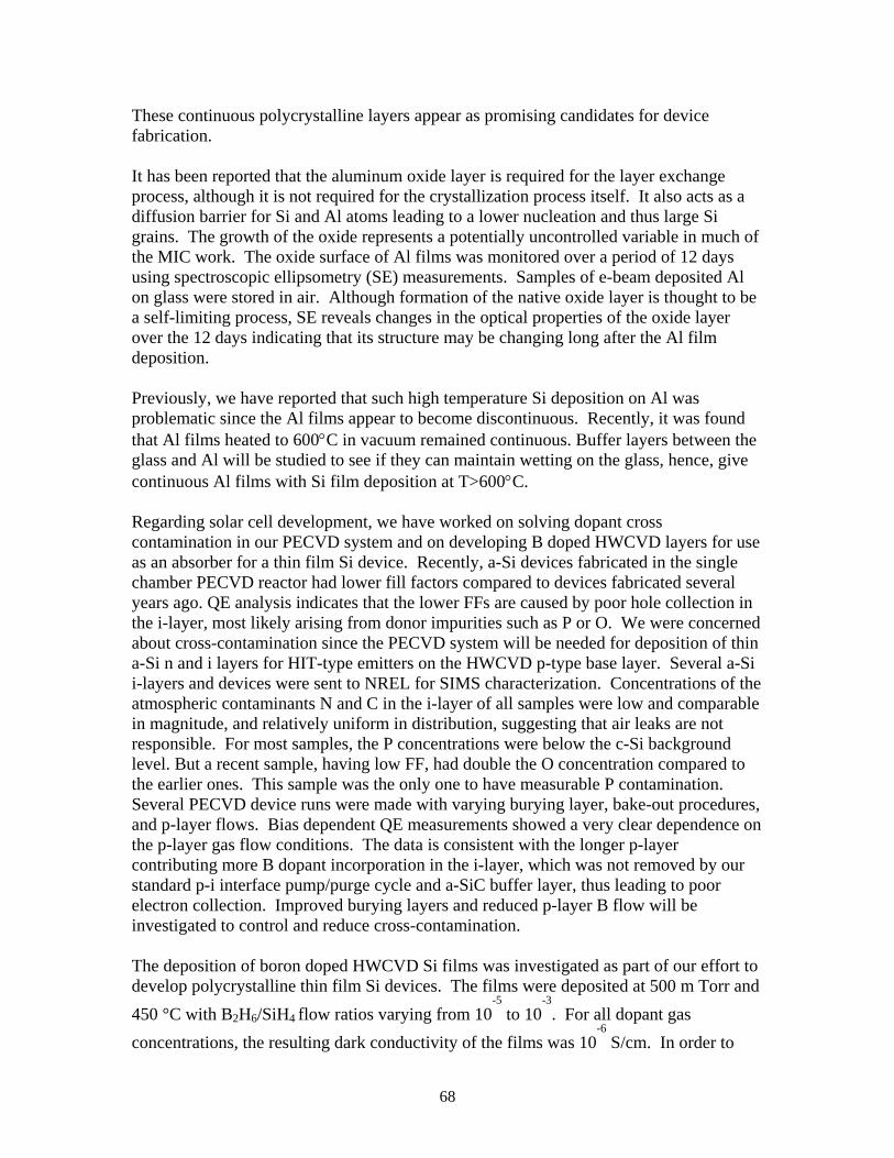
68
These continuous polycrystalline layers appear as promising candidates for device fabrication. It has been reported that the aluminum oxide layer is required for the layer exchange process, although it is not required for the crystallization process itself. It also acts as a diffusion barrier for Si and Al atoms leading to a lower nucleation and thus large Si grains. The growth of the oxide represents a potentially uncontrolled variable in much of the MIC work. The oxide surface of Al films was monitored over a period of 12 days using spectroscopic ellipsometry (SE) measurements. Samples of e-beam deposited Al on glass were stored in air. Although formation of the native oxide layer is thought to be a self-limiting process, SE reveals changes in the optical properties of the oxide layer over the 12 days indicating that its structure may be changing long after the Al film deposition. Previously, we have reported that such high temperature Si deposition on Al was problematic since the Al films appear to become discontinuous. Recently, it was found that Al films heated to 600°C in vacuum remained continuous. Buffer layers between the glass and Al will be studied to see if they can maintain wetting on the glass, hence, give continuous Al films with Si film deposition at T>600°C. Regarding solar cell development, we have worked on solving dopant cross contamination in our PECVD system and on developing B doped HWCVD layers for use as an absorber for a thin film Si device. Recently, a-Si devices fabricated in the single chamber PECVD reactor had lower fill factors compared to devices fabricated several years ago. QE analysis indicates that the lower FFs are caused by poor hole collection in the i-layer, most likely arising from donor impurities such as P or O. We were concerned about cross-contamination since the PECVD system will be needed for deposition of thin a-Si n and i layers for HIT-type emitters on the HWCVD p-type base layer. Several a-Si i-layers and devices were sent to NREL for SIMS characterization. Concentrations of the atmospheric contaminants N and C in the i-layer of all samples were low and comparable in magnitude, and relatively uniform in distribution, suggesting that air leaks are not responsible. For most samples, the P concentrations were below the c-Si background level. But a recent sample, having low FF, had double the O concentration compared to the earlier ones. This sample was the only one to have measurable P contamination. Several PECVD device runs were made with varying burying layer, bake-out procedures, and p-layer flows. Bias dependent QE measurements showed a very clear dependence on the p-layer gas flow conditions. The data is consistent with the longer p-layer contributing more B dopant incorporation in the i-layer, which was not removed by our standard p-i interface pump/purge cycle and a-SiC buffer layer, thus leading to poor electron collection. Improved burying layers and reduced p-layer B flow will be investigated to control and reduce cross-contamination. The deposition of boron doped HWCVD Si films was investigated as part of our effort to develop polycrystalline thin film Si devices. The films were deposited at 500 m Torr and 450 °C with B2H6/SiH4 flow ratios varying from 10
-5 to 10
-3. For all dopant gas
concentrations, the resulting dark conductivity of the films was 10-6
S/cm. In order to

69
understand whether the invariance in conductivity was the result of the deposition conditions or film structure, doped films were deposited with varying thickness. Increasing the thickness by a factor of 3 increases the conductivity by 2 orders of magnitude but did not change the activation energy, indicating an increase in mobility with thickness.
4.4 Phase 4 Summary: 9/5/04 to 9/4/05 Aluminum-induced crystallization (AIC) of Si thin films on glass substrates was investigated as potential techniques leading to continuous large grain Si films. Silicon films were deposited by Hot-Wire Chemical Vapor Deposition (HW-CVD), Plasma Enhanced Chemical Vapor Deposition (PE-CVD) and Electron beam deposition (E-beam) onto Al coated Corning 7059 glass substrates and the annealing of the samples was performed at temperatures below the eutectic temperature of Si-Al binary system (577oC). Both in-situ and ex-situ AIC was evaluated. The grain structure of the polycrystalline silicon (poly-Si) films formed on glass substrates and Al-Si interface were studied by various analytical techniques. Continuous poly-Si films were obtained using Al layers with a thickness of 500 nm or less, and with a Si/Al thickness ratio of at least 1. The average grain size of poly-Si films was affected by the a-Si deposition technique. E-beam deposited a-Si films resulted in 10-15 μm average grain size while PECVD and HWCVD deposited a-Si films resulted in slightly smaller grain sizes. The nature and morphology of the interface oxide layer between Al and Si layers was studied by XPS and were found to be crucial for layer exchange process. The length of time that the Al layer was exposed to air was used to vary the oxide thickness. The effective activation energy for the ex-situ crystallization and layer exchange process was determined to be 0.9 eV. Continuous poly-Si films on glass substrates were obtained using an in-situ aluminum-induced crystallization technique at 430oC. The 0.5 µm Al film was deposited by e-beam and the 0.6 µm Si deposited by HWCVD. Poly-Si films had an average grain size of 10-13 μm, corresponding to a grain size/thickness ratio greater than 20 and similar to poly-Si films prepared by conventional AIC. A unique etching procedure was developed involving repeated cycles of alternately etching the Al then the Si to reveal the continuous Si layer below. Poly-Si layers prepared by either an in-situ or conventional AIC process can be used as seed layers for epitaxial Si growth or for back contact formation in c-Si solar cell fabrication at temperature below 500oC. As an alternative to conventional AIC, the in-situ AIC process eliminates an additional annealing step, which saves considerable time during processing.
4.5 Phase 5 Summary: 9/5/05 to 3/31/07 Aluminum induced crystallization (AIC) of electron beam evaporated amorphous silicon on two substrates, Corning-1737 glass and (100) oriented single crystalline silicon wafer, was evaluated at annealing temperatures below 450oC, and above 600oC, eutectic temperature (EuT), with stacking structure of an a-Si/Al/substrate. Samples were

70
analyzed with optical microscopy, X-ray diffraction, Raman spectroscopy, scanning electron microscopy and energy dispersive spectrometer. For samples grown on glass substrates, continuous crystalline silicon films with grain size of ~ 30µm have been achieved below EuT, while discontinuous crystalline Si “islands” are formed above EuT. For samples grown on Si wafer, no crystallization has been observed below EuT; while above EuT, AIC process occurs with a non-uniform crystalline silicon network formed on the top of the wafer. The crystallized Si films on glass substrate annealed below EuT can be useful as very conductive P-type seed layers for subsequent epitaxial thickening for thin crystalline silicon solar cells on low cost substrates.
Heterojunction c-Si solar cells utilizing a-Si emitters, contacts, and passivation layers have demonstrated high VOC but often with low FFs (S-shape curve). The problem of maintaining high VOC without a loss in FF was studied intently at IEC and was finally solved, leading to an NREL confirmed 17.7% efficiency with VOC =.654 V, FF=76%, and JSC=35.7 mA/cm2. We have also developed a new structure of an all back contact solar cell incorporating silicon heterojunctions. This structure has interdigitated p/n amorphous silicon (a-Si:H) films deposited by plasma-enhanced chemical vapor deposition on the backside of crystalline silicon (c-Si) wafers, with the light irradiating the front surface. Interdigitated back contact Si heterojunction (IBC-SHJ) cells possess advantages over front junction a-Si:H/c-Si heterojunction cells due to minimized current losses in the illuminating side, and over traditional diffused back-junction cells due to low temperature processing combined with the potential of high voltages for the heterojunction. Devices were fabricated on 300 µm thick, polished, n-type float-zone silicon wafer with resistivity of 2.5 Ωcm. The front surface is presently passivated with an intrinsic a-Si:H layer of 20 nm thick deposited by DC plasma enhanced chemical vapor deposition (PECVD) system at 200°C. At the back side of wafer, the contacts are provided by alternating strips of n and p-type interdigitated a-Si:H layers at a thickness of 20 nm. The interdigitated pattern was created by two-step photolithography. The finger-like p-region has lateral dimension of 1.2 mm, while n-region is 0.5 mm wide. The separation between p- and n-regions is ~2 µm, and is formed naturally by undercutting during the etching process. Initial IBC-SHJ cell structures made at IEC have achieved NREL-confirmed cell efficiencies of 11.8% under AM1.5 illumination. We have measured VOC’s of 680 mV. Device results (JV, QE, and lifetime) indicated a strong light intensity dependence. The lowering of the surface recombination velocity as the carrier density increases is due to saturation of the recombination centers. With increasing the illumination level, the carrier density rises dramatically, saturating the recombination centers and increasing the measured minority carrier lifetime. Annealing was found to improve performance of the IBC-SHJ. Fourier transform infrared spectroscopy indicated that bonds at a-Si/c-Si interface are transformed from dihydride to monohydride after annealing. The lowering of defects in the a-Si layer reduces the surface recombination velocity. It was found that the original lifetime 500µs increases to >1ms after annealing.

71
4.6 Phase 6 Summary: 4/1/07 to 12/31/07 The Si effort has been directed towards fabricating, characterizing, and modeling Si solar cells based on n-type Cz wafers with deposited contacts and emitters with the goal of improving VOC. Studies of deposition, structure and electrical properties of thin PECVD Si layers combined with “effective lifetime” measurements, and heterojunction modeling has given insight into mechanisms responsible for improving the effective Si wafer surface passivation. Silicon surface passivation of hydrogenated silicon (Si:H) thin films deposited by radio frequency (RF) and direct current (DC) plasma process was investigated by measuring effective minority carrier lifetime (τeff) on Si (100) and (111) wafers and correlated with the silicon heterojunction (SHJ) cell performances. Apparently the higher ion bombardment in DC compared to RF plasma during growth of a-Si (a-Si:H) layer does not deteriorate Si surface passivation properties. Microstructural defects associated with SiH2 bonding have only a weak influence on τeff. However, any epitaxial growth or presence of crystallinity in the Si:H i-layer severely degrades passivation properties and SHJ cell performance. Excellent surface passivation (τeff > 1 msec) and high efficiency SHJ cells are obtained by both RF and DC plasma-deposited intrinsic a-Si:H buffer layer. High efficiency (>18%) with open circuit voltage (VOC) of 694 mV was achieved on n-type textured Cz wafer using DC plasma process. Interpretation of photovoltaic cell performance through current-voltage testing depends largely on accurate representation of the band structure. This is especially true when considering the numerous interfaces found in a silicon heterojunction (SHJ) cell comprised of deposited a-Si:H emitter, passivation layers, and back contact with a crystalline silicon (c-Si) wafer absorber. Therefore, we determined the electronic levels of the valence and conduction bands, Fermi position, and electron affinity of thin film p-, i-, and n-type a-Si:H as well as (n)c-Si for use in SHJ modelling and performance optimization. Novel application of wet chemically H-terminated a-Si:H enables the study of device quality films to be studied via ultra-violet and X-ray photoemission spectroscopy. It is shown that this H-termination strategy effectively removes native oxide without introducing detectable surface states. The Fermi level varies within a bandgap of ~1.75eV from 1.3 – 0.70eV from the valence band maximum depending on doping and plasma conditions. The electron affinity is measured to be approximately 3.91eV for i-type films, 3.83 for n-type and a surprisingly low 3.37eV for p-type. Also the validity of Fermi level alignment of (p)c-Si/a-Si:H heterojunctions is called into question. An interdigitated back contact silicon heterojunction solar cell has been developed. It combines the high voltage potential of heterojunction solar cells while avoiding the absorption losses in these structures which allows high short circuit currents. This structure has interdigitated p/n a-Si:H-films deposited by low temperature plasma enhanced chemical vapor deposition on the backside of crystalline silicon (c-Si) wafers, with the light irradiating the front surface. The device is attractive for manufacturing due to the all back contact design, the large tolerances in dimensions,

72
low temperature of depositions, and the lack of shunting. Initial solar cells have open circuit voltages of 691 mV but low fill factors. A device was measured at NREL with 11.8% efficiency. High shunt resistance is evidence that the emitter and contact remain isolated despite the relatively simple masking procedure. Two-dimensional modelling is used to explain the present low fill factors obtained with the intrinsic a-Si buffer layer and demonstrates that the structure allows efficiencies in excess of 24%. Very good agreement is shown between measurement of the spatial variation of an LBIC signal across the interdigitated emitter and contacts and the 2D model confirming the assumptions about the device operation and the material parameters used in the model.
Si TFP Team Activity and Industrial Collaboration IEC continued support of Si wafer-based cell development at BP Solar. Deposition of various contact layers and characterization of optical, electrical and junction properties was carried out on their wafers. We assisted Advent Solar in evaluation of anti-reflection and passivation layers on their wafers as well.
Regarding a-Si based thin film PV companies, IEC is supporting Sencera and Sierra Solar in developing their process technology.
4.7 Phase 7 Summary: 1/1/08 to 5/31/08
Passivation of silicon surface with intrinsic a-Si:H The passivation of crystalline silicon surfaces is necessary for high performance devices as the surfaces are areas of high recombination. Amorphous silicon (a-Si) has proved to be an effective passivation layer and here at IEC we have achieved voltages above 700 mV. The level of passivation is dependent on the structure of the deposited amorphous layer. A critical factor in the growth of silicon films is the ratio of hydrogen to silane flow rate denoted here as the R ratio, where a high R ratio indicates a large about of hydrogen dilution.

73
0 2 4 6 8 10100
101
102
103
R (H2/SiH4)
IIIIII
(111)
(100)
RF
DC
DC-i (100) RF-i (100) DC-i (111) RF-i (111)
τ eff
(µse
c)
Figure 1. Effective minority carrier lifetime (τeff) on Si (100) and (111) wafers with 10 nm Si:H i-layer deposited on both sides by RF and DC plasma at variable hydrogen dilution (R). Figure 1 shows τeff as a function of R for i-layers deposited on (100) and (111) wafers by DC and RF plasma after annealing the samples at 280°C for 10 mins. Three distinct regions can be identified in the variation of τeff with R. In region I, R < 2, τeff depends on the plasma process; namely, DC plasma deposited i-layers at R = 0 show slightly lower lifetime, ~ 500 μsec, than RF plasma deposited i-layers, > 1 msec, irrespective of the wafer surface orientation. τeff, however, becomes similar for RF and DC plasma deposited i-layers at R > 2, region II and III, implying little or no adverse effect of ion damage in the DC process on Si surface passivation. In region III, R > 4, the measured τeff exhibits a pronounced Si surface orientation dependence. The values of τeff sharply decrease to < 10 μsec on (100) wafers, while on (111) wafers they remain > 1 msec even at R = 10. In the following section, the DC i-layers are further examined using cross-sectional transmission electron microscopy (XTEM). XTEM images of c-Si / a-Si:H interfaces Figure 2 shows the deposition of a layer of silicon deposited by PECVD on polished crystalline silicon substrates. In image (a), the silicon layer shows a high degree of crystallinity with epitaxial growth so that there is not a clear interface between the substrate and the deposited silicon layer. The lifetime for this sample is low so that the surface is essentially unpassivated as shown in Figure 1 where the R6 lifetime on (100) is only 40 µs.

74
(a) (b) Figure 2. TEM of R6 DC i-layer deposited on silicon substrates. (a) with a (100) orientation and (b) with a (111) orientation. In contrast, the image of (b) shows a completely amorphous layer on top of the crystalline silicon substrate and the lifetime is well above 1 ms. The only difference between the two images is the substrate orientation. The (111) orientation has suppressed crystallinity leading to an amorphous film. To understand the wafer orientation dependence of τeff, i-layer structure and optical properties are determined from VASE measurements on the same samples used for lifetime testing. Figure 3 shows the imaginary part of the pseudo dielectric constant, ε2, as a function of photon energy (E) for i-layers deposited on (100) and (111) wafers at R = 6. A broad featureless spectrum for the R = 6 i-layer on Si (111) wafer is indicative of amorphous Si:H structure. However, the same Si:H layer deposited on (100) wafer exhibits the identical optical constants as crystalline silicon, which implies that the film is
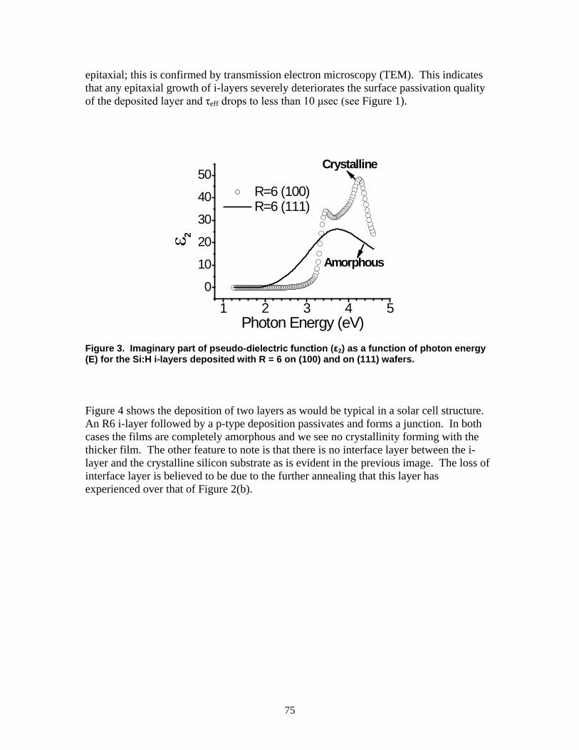
75
epitaxial; this is confirmed by transmission electron microscopy (TEM). This indicates that any epitaxial growth of i-layers severely deteriorates the surface passivation quality of the deposited layer and τeff drops to less than 10 μsec (see Figure 1).
1 2 3 4 50
10
20
30
40
50 R=6 (100) R=6 (111)
Crystalline
Amorphous
ε 2
Photon Energy (eV)
Figure 3. Imaginary part of pseudo-dielectric function (ε2) as a function of photon energy (E) for the Si:H i-layers deposited with R = 6 on (100) and on (111) wafers. Figure 4 shows the deposition of two layers as would be typical in a solar cell structure. An R6 i-layer followed by a p-type deposition passivates and forms a junction. In both cases the films are completely amorphous and we see no crystallinity forming with the thicker film. The other feature to note is that there is no interface layer between the i-layer and the crystalline silicon substrate as is evident in the previous image. The loss of interface layer is believed to be due to the further annealing that this layer has experienced over that of Figure 2(b).

76
Figure 4. R6 DC i-layer and p-layer on (111) Si substrate. The XTEM final image is for a deposition on (111) material where there is a very high dilution of the growth with hydrogen and R = 40. In this case we get the growth of a microcrystalline film on the substrate. The crystal structure of the film is very poor unlike that of Figure 2(a) where epitaxial growth was seen. The loss of amorphous film has caused a loss of passivation in this layer and the lifetime has dropped to under 100 µs.

77
Figure 5. R40 DC i-layer and p-layer on (111) Si substrate. The XTEM images show that good passivation and low surface recombination is only achieved with an amorphous film. Amorphous films grow more readily on (111) surfaces and by using layers with a lower hydrogen dilution.
Fabrication of Back Junction Devices Figure 6(a) shows the schematic structure of the front silicon heterojunction (SHJ) and interdigitated back contact-silicon heterojunction (IBC-SHJ) cells. All the a-Si:H layers are deposited using identical plasma conditions in both cell structures. The i-layers are deposited with R = 2 to suppress the growth of microcrystalline silicon. The illuminated J-V curves are compared in Figure 6(b). The VOC values (~690 mV) are the same in both structures, while JSC is higher (~ 3 mA/cm2) in the IBC structure due to reduced optical loss at the front illuminating side. However, the FF in this IBC structure is very low due to the “S” shape J-V curve. This result indicates the necessity of further optimization of IBC-SHJ solar cells. There are two major functional differences between the front-junction and IBC device structures: (i) the carrier transport is one dimensional in front-junction SHJ cell, while the IBC-SHJ structure has a two dimensional transport mechanism, and (ii) the front i-layer in front-junction SHJ cell gets illuminated and generates photo carriers, while the i-layer in the IBC structure is in the dark and does not generate carriers.

78
(i) a-Si:H
(i) a-Si:Hn-type wafer
(n) a-Si:H
ITO
Al
(p) a-Si:H
Al grids
(a)
(p)/(n) a-Si:H
n-type wafer
~50 µm
AR coating
Al Al Al
(b) (i) a-Si:H
(i) a-Si:H
(i) a-Si:H
(i) a-Si:Hn-type wafer
(n) a-Si:H
ITO
Al
(p) a-Si:H
Al grids
(a)(i) a-Si:H
(i) a-Si:Hn-type wafer
(n) a-Si:H
ITO
Al
(p) a-Si:H
Al grids
(a)
(p)/(n) a-Si:H
n-type wafer
~50 µm
AR coating
Al Al Al
(b) (i) a-Si:H
(i) a-Si:H(p)/(n) a-Si:H
n-type wafer
~50 µm
AR coating
Al Al Al
(b) (i) a-Si:H
(i) a-Si:H0.0 0.1 0.2 0.3 0.4 0.5 0.6 0.7 0.8
-10-505
10152025303540
IBC-SHJ Front SHJ
Curr
ent D
ensi
ty (m
A/cm
2 )
Voltage (V)
(c)
Figure 6. Schematic structures of (a) front junction SHJ cell, (b) IBC-SHJ cell, and (c) comparison of the illuminated J-V curves in two cell structures.
2D numerical simulation of IBC-SHJ solar cell
Figure 7. Simulated J-V curves for IBC-SHJ cells [structure shown in Figure 8 (b)] under illumination with variable band gap of the intrinsic a-Si buffer layer. We have performed 2D numerical simulation using a “Sentaurus Device” simulator (called DESSIS in its old version). Both the experimental results and numerical simulation confirm that low FF with an “S” shape J-V appears in IBC-SHJ structure due to the presence of an intrinsic a-Si:H buffer layer only in the p-type emitter strip. This suggests the existence of a hole transport barrier across the intrinsic a-Si:H buffer layer. The low FF and “S” shape J-V can arise from the hole transport barrier due to the enhanced valence band offset generated by the intrinsic buffer layer. Hence the effect of band gap of the intrinsic a-Si buffer layer on IBC-SHJ cell performance is studied. Again, the surface passivation effects of the different buffer layers are assumed to be the same, while electron affinities of the buffer layers are assumed constant. Figure 7 shows the illuminated J-V characteristics obtained from simulation for intrinsic a-Si buffers as a function of band gaps. A substantial effect of the band gap is evident on FF, which increases from 55% to >78% as the band gap of the buffer layer is reduced by 0.07 eV.
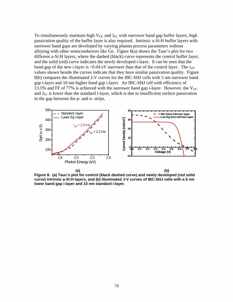
79
To simultaneously maintain high VOC and JSC with narrower band gap buffer layers, high passivation quality of the buffer layer is also required. Intrinsic a-Si:H buffer layers with narrower band gaps are developed by varying plasma process parameters without alloying with other semiconductors like Ge. Figure 8(a) shows the Tauc’s plot for two different a-Si:H layers, where the dashed (black) curve represents the control buffer layer, and the solid (red) curve indicates the newly developed i-layer. It can be seen that the band gap of the new i-layer is ~0.04 eV narrower than that of the control layer. The τeff values shown beside the curves indicate that they have similar passivation quality. Figure 8(b) compares the illuminated J-V curves for the IBC-SHJ cells with 5 nm narrower band gap i-layer and 10 nm higher band gap i-layer. An IBC-SHJ cell with efficiency of 13.5% and FF of 77% is achieved with the narrower band gap i-layer. However, the VOC and JSC is lower than the standard i-layer, which is due to insufficient surface passivation in the gap between the p- and n- strips.
1.8 2.0 2.2 2.4
100
200
300
400
500
τeff = 1.0 ms
Standard i-layer Lower Eg i-layer
Sqrt
(α x
E)
Photon Energy (eV)
τeff = 1.2 ms
0.0 0.1 0.2 0.3 0.4 0.5 0.6 0.7 0.8
-10
0
10
20
30
40 Std 10nm intrinsic layer Low Eg 5nm intrinsic layer
Curre
nt D
ensit
y (m
A/cm
2 )
Voltage (V)
(a) (b) Figure 8. (a) Tauc’s plot for control (black dashed curve) and newly developed (red solid curve) intrinsic a-Si:H layers, and (b) illuminated J-V curves of IBC-SHJ cells with a 5 nm lower band gap i-layer and 10 nm standard i-layer.
80
5 IN-LINE DIAGNOSTICS AND PROCESS CONTROL 5.1 Phase 1 Summary: 9/5/01 to 9/4/02 Widespread use of photovoltaic technology is hindered by its high costs. One of the most promising strategies for lowering PV costs is the use of thin film technologies in which the PV materials are deposited onto inexpensive large area substrates such as window glass and flexible substrates. Benefiting from the inherent advantages to thin film PV will require breakthroughs in reducing manufacturing costs, primarily by improving yields and increasing throughput. A critical requirement to improve manufacturing yields is the development diagnostics tools and associated predictive models that quantitatively assess processing conditions and product properties. Incorporation of the diagnostic sensors into both laboratory reactors and manufacturing facilities will: 1) underpin the development of solar cells modules with improved efficiency; and 2) accelerate the scale-up process through model-base process control schemes. In-situ, in- line diagnostics tools are needed for process and product quality control, as well as, non-destructive testing for off-line product evaluation. Currently, diagnostic capabilities required for manufacturing large area thin film modules are in their infancy and all thin-film manufacturers can only assess their product after completion of the module. Under this task, a preliminary survey of available sensor technologies was performed which focused primarily on product diagnostics to evaluate film properties such as thickness, composition, crystallinity and grain size, and optical bandgap and changes structural and chemical changes during processing. The sensors consider where ellipsometry, X-ray diffraction/fluorescence, and infrared spectroscopy techniques as well as atomic absorption spectroscopy as a process control sensor. 5.2 Phase 2 Summary: 9/5/02 to 9/4/03 Contact wetting angle, ellipsometry and glancing incidence x-ray diffraction are surface sensitive technique methods that are under investigation as diagnostic tools for thin-film processing. An apparatus for carrying out contact angle measurements was constructed and wetting angle measurements are being carried out on different types of samples to determine the sensitivity to changes in surface energy arising from thin-film processing. Ellipsometry is being developed to determine film composition in multi-layer thin-film structures such as treated CdTe surfaces. Glancing x-ray diffraction is being developed to determine residual stress in thin films and the thickness of surface layers obtained on CdTe films under different post-deposition processing conditions and to evaluate residual stress in as-deposited Mo films.

81
5.3 Phase 3 Summary: 9/5/03 to 9/4/04 The in-line process diagnostic effort is intended to develop the tools needed for process control and quantitative models to link sensor output to process variables to material properties. Commercial-scale PV module fabrication would benefit from methods to analyze thin-film surfaces at various stages of processing. Contact wetting angle measurement is a simple diagnostic tool that may be suitable in industrial applications for monitoring changes in thin film solar cell processing conditions. The terminating surface of a solid is known to contain excess free energy when compared to the bulk. Surface energies (EP) consist of polar energies (ED) resulting from permanent and induced dipole moments as well as hydrogen bonding, and dispersive energies that arise from vibrational interactions between atoms. The interaction of liquids and solids of different surface energies are known to give rise to the formation of characteristic angles known as wetting angles at a liquid/solid interface. Wetting angles were recorded for water droplets deposited onto CdTe surfaces at varying times over the course of an hr immediately (<1 min) upon removal from the evacuated deposition chamber, during exposure to air and after subsequent chemical etching for 5 sec. in a bromine-methanol solution. A CdTe film tested upon removal from the deposition chamber (as-dep) nearly completely wet the entire surface of the sample (θ ~1o). Rapid increases in this value were observed over the first hr. Bromine-methanol etched films, however, experienced differing effects with respect to the magnitude of the wetting angle, which increased rapidly during the first 20 min then subsequently decreased nearly as swiftly implying that etching does not produce surfaces similar to that of as-deposited CdTe. The rate of change in wetting angles was greatest within the first hr of exposure to the atmosphere for both as-deposited and etched CdTe. CdTeO3 is the predominant native oxide of CdTe. Changes in the magnitude of wetting angle can therefore be attributed to the formation of the native oxide CdTeO3 for as-dep CdTe and in-part for the etched CdTe. For etched CdTe it is hypothesized that initially a thin amorphous Te layer is generated which begins to crystallize over a twenty-min period and then subsequently oxidizes to TeO2, the predominant native oxide for Te. The results of processing on the surface energies of PVD CdTe were studied. The oxides that are formed or removed as a result of processing primarily affect Ep leaving Ed largely unchanged, however, contact wetting was unable to differentiate between the formation of different oxide phases. Surface oxidation resulting from CdCl2 treatment increased Ep, by 9.8, 8.7, and 5.9 mN/m for vacuum, dry air, and saturated air stored samples, respectively. Etching in Br2:CH3OH reduced Ep by 4.4, 16.8, and 9.6 mN/m due to the removal of oxides from the film surfaces for vacuum, dry air, and saturated air stored samples, respectively. Effects of crystallization of ITO were evaluated for atmospheres containing air and argon. Energy changes may be attributed to higher surface polarity associated with the alignment and organization of bonds from previously amorphous states.

82
Thus, contact wetting is a simple and effective tool that is able to detect changes in surface energies resulting from post deposition processing. As-deposited CdTe seeks to satisfy dangling bonds through reaction with air ambient. Significant native oxidation of PVD (111) CdTe occurs within hours upon exposure to the atmosphere and can be observed by increases in wetting angles. Dry air storage of CdTe prior to CdCl2 heat treatments forms beneficial (CdO) oxides while films kept in saturated air produce electronically detrimental CdTe2O5 on surfaces. Polar energies increase as a result of oxides formed during treatment and decrease upon removal via chemical etching. 5.4 Phase 4 Summary: 9/5/04 to 9/4/05 A wide range of thin film analyses using GIXRD were surveyed for implementation into thin film PV device fabrication as a diagnostic and monitoring tool. Construction of a hot stage allowed in-situ detection of CdTe surface oxidation and CdTe-CdS interdiffusion. The oxidation studies were complimented by compositional depth profiling by XPS using the system installed in 2005. Te film thickness on etched CdTe was determined by regression of a layer model with measured data at different incident beam angles. A unique solution is facilitated by considering primary beam attenuation in the Te film. Dual-axis GIXRD measurements of multiple (hkl) reflections allowed determination of depth-distribution of residual stress in sputtered Mo films. For ultra-thin CdS films with nanometer size particulates, the particulate size was determined by fitting the GIXRD line profile and evaluating the integral line breadth. Alloy distribution in CuIn1-xGaxSe2 films was determined by modeling GIXRD patterns obtained at different incident beam angles and verified by measuring a CuIn1-xGaxSe2 film from both sides. This methodology is being used to investigate reaction pathways for obtaining films with uniform composition and could be used as a product sensor in a developed process. 5.5 Phase 5 Summary: 9/5/05 to 3/31/07 Elemental sources used in CuInGaSe2 thin film deposition process have been investigated and characterized for the purpose of developing rules to facilitate the process scale-up. Finite-element-based thermal modeling on the linear source-boat using the COMSOL Multiphysics software package showed that there is a temperature gradient along the source. The temperature was found to be cooler on the end where heater leads are connected. Thermocouple location that best estimates melt surface temperature was obtained through FEMLAB thermal simulation. Furthermore, properly placed thermocouples were shown to give accurate melt surface temperature independent of the melt level in the source. In an experiment, melt temperatures were then estimated along the operating Cu source through the thermocouples placed accordingly. The melt temperature did show the similar non-uniformity as was obtained from finite-element modeling. The non-uniformity was also observed in the Cu film thickness deposited on a substrate placed along the source. In addition, Direct Simulation Monte Carlo Technique was used to develop a more refined estimation of the effusion rates and flux distribution from the sources.
83
5.6 Phase 6 Summary: 4/1/07 to 12/31/07 Process diagnostics are critical to evaluate and monitor the processing of thin film solar cells to maintain yield and avoid a large amount of off-spec production. To implement process diagnostics in real time requires both process and product monitoring as well as process control. Previous reports have contained our work on using contact wetting angle and X-ray diffraction as process monitors. During this period, graduate student Kapil Mukati completed his dissertation, “An alternative structure for next generation regulatory controllers and scale-up of Cu(InGa)Se2 thin film co-evaporative physical vapor deposition process” awarded by the Department of Chemical Engineering for research conducted at IEC under the direction of Drs. Birkmire and Eser. It describes the process control needed to implement in-line real-time process diagnostics. A summary of that research is contained here. Further details may be found in his dissertation. Process control systems have three key performance attributes: Set-point tracking (T) is ability to cause the process output to follow set-point changes rapidly and faithfully; Disturbance rejection (D) is the ability to counteract the effects of external disturbances; and Robustness (R) the ability to remain stable and perform well in the face of inevitable plant/model mismatch. A controller whose tuning constants are related directly to these performance attributes will have definite advantages over other controllers. However, the popular PID controller, even though simple, has an intrinsic structure that results in a complicated, hence non-transparent, relationship between its tuning parameters and the three controller performance attributes, limiting the controller’s achievable performance and making tuning more complex than necessary. In order to overcome the weaknesses of the PID controller, we have developed an alternative regulatory controller [the Robustness, Tracking, Disturbance rejection, and overall Aggressiveness (RTDA) controller] having the following salient features: it requires precisely the same information that is required for tuning PID controllers; its tuning parameters are directly related to the three key controller attributes of R, T, and D [an auxiliary fourth parameter, influences the overall controller aggressiveness (A)]; all four tuning parameters are normalized to lie between 0 and 1; and the magnitude of a tuning parameter is related to performance aggressiveness, where the higher magnitudes signify conservative performance in the attribute of interest. In addition, the proposed predictive controller is not any more complicated to implement, in either software or hardware, than the PID controller.
In order to study how the choices of various RTDA controller parameter values jointly and individually affect closed-loop stability, a theoretical robust stability analysis is performed. The results of this analysis are subsequently used to develop systematic strategies for choosing the RTDA controller parameters that provide the best possible trade-off between robust stability and performance. The design and implementation of the RTDA controller in practice are illustrated experimentally using two processes: a lab-scale four-tank process with time delay and a pilot-scale physical vapor deposition process with nonlinear dynamics. These experiments demonstrate the RTDA controller’s
84
improved performance over PID controllers. The RTDA control scheme is also extended to integrating and open-loop unstable processes.
A pilot-scale co-evaporative physical vapor deposition (PVD) process for manufacture of copper indium gallium diselenide (Cu(InGa)Se2) thin films is chosen to validate the proposed RTDA controller experimentally, since robust control of film thickness and composition set-points for long deposition times cannot be achieved without effective base regulatory control. However, unlike film thickness and composition set-points that can be achieved with proper process control, achieving film thickness uniformity across large area substrates is a process design issue. To achieve good process performance, the process design issues are addressed first, and then the regulatory controller design is improved.
The work presented in Part II of this thesis is focused mainly on the evaporation source design. Such a study requires not only the detailed knowledge of the evaporation source temperature profile, but also accurate estimation of nozzle flow properties (effusion rates and vapor flux distribution). A three-dimensional first-principles electro-thermal model of the source is developed using the COMSOL MultiphysicsTM finite-element method, and the Direct Simulation Monte Carlo (DSMC) technique is employed to predict accurately the nozzle flow properties for any given nozzle geometry and evaporant. These models are validated experimentally, and subsequently used to design evaporation sources that not only achieve the targeted film thickness uniformity, but also maximize the material utilization efficiency. Results of this work were reported in IEC’s previous annual report.
85
6 PUBLICATIONS 2001 "Hot-Wire Chemical Vapor Deposition of Silicon from Silane: Effect of Process Conditions," Atul Pant, T.W.F. Russell, Marylin C. Huff, Roger Aparicio and Robert W. Birkmire, Ind. Eng. Chem. Res. 49(5), 1377 (2001). “Reactor and Reaction Model for the Hot-Wire Chemical Vapor Deposition of Silicon from Silane,” Atul Pant, Marylin C Huff, and T.W.F. Russell, Ind. Energy Chem. Res. 40(5), 1386 (2001). "Interdiffusion of CdS/CdTe Thin Films: Modeling X-ray Diffraction Line Profiles," Brian E. McCandless, Michael G. Engelmann and Robert W. Birkmire, J. Appl. Phys. 89(2), 988 (2001). “Initial and Stressed Performance of CdTe Solar Cells: Effect of Contact Processing,” S. S. Hegedus, B. E. McCandless and R.W. Birkmire, Proc. NCPV Prog. Rev. Mtg., 119 (2001). “Thin Si p-layers Containing Boron Doped Micro-crystalline Si and a-SiOx Phases,” E. Eser, W. Buchanan and S. Hegedus, Proc. NCPV Prog. Rev. Mtg., 183 (2001). “Wide Band Gap CuInSe2 and CdTe-based Thin Films for Tandem Solar Cells,” W. Shafarman, M. Gossla, B. McCandless, Proc. NCPV Prog. Rev. Mtg., 229 (2001). “Optical, Structural and Transport Properties of Reactively Sputtered ZnTe:N, J. Drayton, C. Taylor, A. Gupta, R.G. Bohn, A.D. Compaan, B.E. McCandless and D. Rose, Proc. NCPV Prog. Rev. Mtg, 243 (2001). "Post-Deposition Sulfur Incorporation into CuInSe2 Thin Films," Jochen Titus, Hans-Werner Schock, Robert W. Birkmire, William N. Shafarman and Udai P. Singh, Mater. Res. Soc. Symp.Proc. 668, H1.5.1 (2001). "Thermochemical and Kinetic Aspects of Cadmium Telluride Solar Cell Processing," Brian E. McCandless, Mater. Res. Soc. Symp. Proc. 668, H1.6.1 (2001). "Effect of Grain Size, Morphology and Deposition Temperature on Cu(InGa)Se2 Solar Cells," William N. Shafarman and Jie Zhu, Mater. Res. Soc. Symp. Proc. 668, H.2.3.1 (2001). "Optically Assisted Metal-Induced Crystallization of Thin Si Films for Low-Cost Solar Cells," Wei Chen, Bhushan Sopori, Kim Jones, Robert Reedy, N.M. Ravindra, Roger Aparicio, Robert Birkmire, Scott Morrison, Ken Coats and Arun Madan. Mater. Res. Soc. Symp. Proc. 685, D32.1 (2001).
86
"Process Analysis and Modeling of Thin Silicon Film Deposition by Hot-Wire Chemical Vapor Deposition," R. Aparicio, R. Birkmire, A. Pant, M. Huff, T.W.F. Russell, Proc. 199th Electrochemical Soc. Mtg. 2001-13, 260 (2001). "Characterization of Deep Defects in CuIn1-xGaxSe2 (CIGS) Working Photovoltaic Devices," J.T. Heath, J.D. Cohen, W.N. Shafarman and D.C. Johnson, Proc. 199th Electrochemical Soc. Mtg. 2001-10, 324 (2001). "Compound Polycrystalline Solar Cells: Recent Progress and Y2K Perspective," Robert W. Birkmire, Solar Energy Mat. & Solar Cells 65, 17 (2001). "Study of Cd-free Buffer Layers Using Inx(OH,S)y on CIGS Solar Cells," C.H. Huang, Sheng S. Li, W.N. Shafarman, C.-H. Chang, E.S. Lambers, L. Rieth, J.W. Johnson, S. Kim, B.J. Stanbery, T.J. Anderson and P.H. Holloway, Solar Energy Mat. & Solar Cells 69, 131 (2001). "Formation and Analysis of Graded CuIn (Se1-ySy)2 Films," M. Engelmann, B.E. McCandless and R.W. Birkmire, Thin Solid Films 387, 14 (2001). ”Chalcogenide Solar Cells Grown by Physical Vapor Deposition Technique,” N. Barreau, S. Marsillac, J.D. Bernede and W.N. Shafarman, Proc. 17th Euro. PVSEC and Exhibition, 215 (2001). 2002 "Cu(In1-xAlx)Se2 Thin Films and Solar Cells," P.D. Paulson, M.W. Haimbodi, S. Marsillac, R.W. Birkmire and W.N. Shafarman, J. Appl. Phys. 91(12), 10153 (2002). “Effect of Plasma and Thermal Annealing on Optical and Electronic Properties of SnO2 Substrates Used for a-Si Solar Cells,” Steven S. Hegedus, J. Appl. Phys. 92(1), 620 (2002). “Phase Behavior in the CdTe-CdS Pseudobinary System,” Brian E. McCandless, Gregory M. Hanket, D. Garth Jensen, and Robert W. Birkmire, J. Vac. Soc. Technol. A. 20(4), 1462 (2002). “High Efficiency Solar Cells Based on Cu(InAl)Se2 Thin Films,” S. Marsillac, P.D. Paulson, M.W. Haimbodi, R.W. Birkmire and W.N. Shafarman, Appl. Phys. Lett. 81(7), 1350 (2002). “Cadmium Zinc Telluride Films for Wide Band Gap Solar Cells,” Brian E. McCandless, Proc. 29th IEEE PVSC, 488 (2002).

87
“Material and Device Characterization of Thin Film Cu(InAl)Se2 Solar Cells,” W.N. Shafarman, S. Marsillac, P.D. Paulson, M.W. Haimbodi, T. Minemoto, and R.W. Birkmire, Proc. 29th IEEE PVSC, 519 (2002). “Properties of Reactively Sputtered ZnTe:N and Its Use in Recombination Junctions,” J. Drayton, C. Taylor, A. Gupta, R.G. Bohn, G. Rich, A.D. Compaan, B.E. McCandless, and D. Rose, Proc. 29th IEEE PVSC, 539 (2002). “Vapor Transport Deposition of Cadmium Telluride Films,” Brian E. McCandless, Robert W. Birkmire, Wayne A. Buchanan, Shannon Fields, Gregory M. Hanket, Proc. 29th IEEE PVSC, 547 (2002). “Pilot-scale Manufacture of Cu(InGa)Se2 Films on a Flexible Polymer Substrate,” Gregory M. Hanket, Udai P. Singh, Erten Eser, William N. Shafarman, and Robert W. Birkmire, Proc. 29th IEEE PVSC, 567 (2002). “Correlation Between Deep Defect States and Device Parameters in CuIn1-xGaxSe2 Photovoltaic Devices,” Jennifer T. Heath, J. David Cohen, William N. Shafarman, Proc. 29th IEEE PVSC, 596 (2002). “Study of a New Indium Sulphide Derivative for Buffer Layer Application,” N. Barreau, S. Marsillac, J.C. Bernede, C. Deudon, L. Brohan, W.N. Shafarman, A. Barreau, Proc. 29th IEEE PVSC, 628 (2002). “Investigation of Chemical-Bath-Deposited ZnS Buffer Layers for Cu(InGa)Se2 Thin Film Solar Cells,” Baosheng Sang, William N. Shafarman, and Robert W. Birkmire, Proc. 29th IEEE PVSC, 632 (2002). “Substrate and Back Contact Effects in CIGS Devices on Steel Foil,” W.K. Batchelor, M.E. Beck, R. Huntington, I.L. Repins, A. Rockett, W.N. Shafarman, F.S. Hasson, J.S. Britt, Proc. 29th IEEE PVSC, 716 (2002). “Optical Design and Analysis of Textured a-Si Solar Cells,” Steven Hegedus, Bhushan Sopori, P.D. Paulson, Proc. 29th IEEE PVSC, 1122 (2002). “Ionizing Radiation Effects in Copper Indium Gallium Diselenide Thin-film Solar Cells,” J. Tringe, J. Nocerino, R. Tallon, W. Kemp, W. Shafarman, D. Marvin, J. Appl. Phys. 91(1), 516 (2002). “Effect of Ga Content on Defect States in CuIn1-xGaxSe2 Photovoltaic Devices,” J. T. Heath, J.D. Cohen, W.N. Shafarman, D.X. Liao and A.A. Rockett, Appl. Phys. Lett. 80(24), 4540 (2002). “Analysis of Quantum Efficiency and Optical Enhancement in Amorphous Si p-i-n Solar Cells,” Steven S. Hegedus and Ruhi Kaplan, Prog. Photovolt:Res. Appl. 10, 257 (2002).

88
2003 “Deposition and Structural Characterization of Poly-Si Thin Films on Al-coated Glass Substrates Using Hot-wire Chemical Vapor Deposition,” Ozgenc Ebil, Roger Aparicio, Sutki Hazra, Robert W. Birkmire, Eli Sutter, Thin Solid Films 430, 120 (2003). “Correlation of Surface Phases with Electrical Behavior in Thin-film CdTe Devices,” B.E. McCandless, S.S. Hegedus, R.W. Birkmire, D. Cunningham, Thin Solid Films 431, 249 (2003). “Near-Surface Defect Distributions in Cu(In,Ga)Se2,” A. Rockett, D. Liao, J.T. Heath, J.D. Cohen, Y.M. Strzhemechnym L.J. Brillson, K. Ramanathan, W.N. Shafarman, Thin Solid Films 431, 301 (2003). “New Cd-free Buffer Layer Deposited by PVD:In2S3 Containing Na Compounds.” N. Barreau, J.C. Bernede, S. Marsillac, C. Amory, W.N. Shafarman, Thin Solid Films 431, 326 (2003). “Distinguishing Metastable Changes in Bulk CIGS Defect Densities From Interface Effects,” J.T. Heath, J.D. Cohen, W.N. Shafarman, Thin Solid Films 431, 426 (2003). “Optical Characterization of CuIn1-xGaxSe2 Alloy Thin Films by Spectroscopic Ellipsometry,” P.D. Paulson, R.W. Birkmire, W.N. Shafarman, J. Appl. Phys. 94(2), 879 (2003). “Critical Issues for Cu(InAl)Se2 Thin Film Solar Cells,” W.N. Shafarman, S. Marsillac, T. Minemoto, P.D. Paulson, R.W. Birkmire, Proc. WCPEC-3, 2869 (2003). “CuxS Back Contact for CdTe Solar Cells,” Donghwan Kim, Brian E. McCandless, Steven S. Hegedus, and Robert W. Birkmire, Proc. WCPEC-3, (2003). “Role of Process Chemistry and Stability on CdTe-based Solar Cell Performance,” B. McCandless, K. Dobson, S. Hegedus, and P. Paulson, Proc. NCPV Rev. Mtg., 401 (2003). “Advances in CuInSe2-based Solar Cells: From Fundamentals to Processing,” W. Shafarman, J. Titus, M. Haimbodi, M. Gossla, G. Hanket, S. Marsillac, T. Minemoto, P. Paulson, B. Sang, U. Singh, E. Eser, R. Birkmire, Proc. NCPV Prog. Rev. Mtg., 525 (2003). “Growth and Characterization of HWCVD Si Films on Al Coated Glass,” by O. Ebil, R. Aparicio, S. Hegedus and R. Birkmire, Proc. NCPV Rev. Mtg., 813 (2003). “The Dynamics of Cadmium Telluride Etching,” K.D. Dobson, P.D. Paulson, B.E. McCandless, R.W. Birkmire, Mater. Res. Soc. Symp. Proc. 763, 107 (2003).

89
“Sputtered ZnTe:N and ZnO:Al for Solar Cell Electrodes and Recombination Junctions,” Jennifer Drayton, V. Parikh, G. Rich, A. Gupta, T. Osborn, R.G. Bohn, A.D. Compaan, B.E. McCandless, P.D. Paulson, Mater. Res. Soc. Symp. Proc. 763, 353 (2003). “New Junction Capacitance Methods for the Study of Defect Distributions and Carrier Properties in the Copper Indium Diselenide Alloys,” J. David Cohen, Jennifer T. Heath, and William N. Shafarman, Mater. Res. Soc. Symp. Proc. 763, 429 (2003). “Photoconductive CdS: How Does It Affect CdTe/CdS Solar Cell Performance?” S. Hegedus, D. Ryan, K. Dobson, B. McCandless, D. Desai, Mater. Rec. Soc. Symp. Proc. 763, 447 (2003). “Defects in Copper Indium Aluminum Diselenide Films and their Impact on Photovoltaic Device Performance,” Jennifer T. Heath, J. David Cohen, William N. Shafarman, Mater. Res. Soc. Symp. Proc. 763, B.9.2.1 (2003). “Chemical Surface Deposition of Ultra-Thin Cadmium Sulfide Films for High Performance and High Cadmium Utilization,” Brian E. McCandless, William N. Shafarman, Proc. PVSEC-3, 562 (2003). “Status, Trends, Challenges, and the Bright Future of Solar Electricity from Photovoltaics,” S. Hegedus, A. Luque, Handbook of Photovoltaic Science and Engineering, Chapter 1 (A. Luque and S.S. Hegedus, eds.), Wiley and Sons, Chichester, UK, 1 (2003). “Cu(InGa)Se2 Solar Cells,” W.N. Shafarman, L. Stolt, Handbook of Photovoltaic Science and Engineering, Chapter 13” (A.. Luque and S.S. Hegedus, eds.), Wiley and Sons, Chichester, UK, 567 (2003). “Cadmium Telluride Solar Cells,” B.E. McCandless, J. Sites, Handbook of Photovoltaic Science and Engineering, Chapter 14“ (A. Luque and S.S. Hegedus, eds.), Wiley and Sons, Chichester UK, 617 (2003). “Determination of Activation Barriers for the Diffusion of Sodium Through CIGS Thin-Film Solar Cells,” M.B. Zellner, R.W. Birkmire, E. Eser, W.N. Shafarman and J.G. Chen, Prog. Photovolt: Res. Appl. 11(8), 543 (2003). “Correlation of Surface Phases with Electrical Behavior in Thin-Film CdTe Devices,” B.E. McCandless, S.S. Hegedus, R.W. Birkmire and D. Cunningham, Thin Solid Films 431-432, 249 (2003). "Formation and Characterization of Electroless-Deposited NiTe2 Back Contacts to CdTe/CdS Thin-Film Solar Cells," Kevin D. Dobson, Ofer Rotlevi, Doug. Rose and Gary Hodes, J. Electrochem. Soc. 149(2), G147 (2003).

90
“Factors Affecting the Stability of CdTe/CdS Solar Cells, Deduced from Stress Tests at Elevated Temperature,” I. Visoly-Fisher, K. D. Dobson, J. Nair, E. Bezalel, G. Hodes, D. Cahen, Adv. Funct. Mater. 13, 289 (2003). “Deposition and Structural Characterization of Poly-Si Thin Films on Al-coated Glass Substrates Using Hot-wire Chemical Vapor Deposition,” Ozgenc Ebil, Roger Aparicio, Sutki Hazra, Robert W. Birkmire, Eli Sutter, Thin Solid Films 430, 120 (2003). 2004 “Bulk and Metastable Defects in CuIn1-xGaxSe2 Thin Films Using Drive-level Capacitance Profiling,” Jennifer T. Heath, J. David Cohen, William N. Shafarman, J. Appl. Phys. 95(3), 1000 (2004). “Optical Properties of Cd1-xZnxTe Films in a Device Structure Using Variable Angle Spectroscopic Ellipsometry,” P.D. Paulson, B.E. McCandless, and R.W. Birkmire, J. Appl. Phys. 95(6), 3010 (2004). “Improved Fill Factors in Amorphous Silicon Solar Cells on Zinc Oxide by Insertion of a Germanium Layer to Block Impurity Incorporation,” G. Ganguly, D.E. Carlson, S.S. Hegedus, D. Ryan, R.G. Gordon, D. Pang, R.C. Reedy, Appl. Phys. Lett. 85(3), 479 (2004). “Physical Characterization of Thin-film Solar Cells,” Ken Durose, Sally E. Asher, Wolfram Jaegermann, Dean Levi, Brian E. McCandless, Wyatt Metzger, Helio Moutinho, P.D. Paulson, Craig L. Perkins, James R. Sites, Glenn Teeter and Mathias Terheggen, Prog. Photovolt: Res. Appl. 12, 177 (2004). “Manufacture of Thin-Film Solar Cells: Modeling and Control of Cu(InGa)Se2 Physical Vapor Deposition onto a Moving Substrate,” Sven Tobias Junker, Robert W. Birkmire, Francis J. Doyle, III, Ind. Eng. Chem. Res. 43, 566 (2004). “Surface Sulfurization of Thin Film Cu(InGa)Se2 Solar Cells” Udai P. Singh, William N. Shafarman, and Robert W. Birkmire, Technical Digest of Int’l PVSEC-14 1-136, 607 (2004). “Thin-Film Solar Cells: Device Measurements and Analysis,” Steven S. Hegedus, and William N. Shafarman, Prog. Photovolt: Res. Appl. 12(3), 155 (2004). “Thin-Film Solar Cells: An Overview,” K. L. Chopra, P. D. Paulson and V. Dutta, Prog. Photovolt: Res Appl. 12, 69 (2004). “Spectroscopic Ellipsometry Investigation of Optical and Interface Properties of CdTe Films Deposited on Metal Foils,” P.D. Paulson and Xavier Matthew, Solar Energy Mat. & Solar Cells 82, 279 (2004).
91
“Material and Device Properties of Single-Phase Cu(In,Ga)(Se,S)2 Alloys Prepared by Selenization/Sulfurization of Metallic Alloys,” V. Alberts, J. Titus, R.W. Birkmire, Thin Solid Films 451-452, 207 (2004). “Accurate Determination of Optical Constants of Textured SnO2 Using Low Incidence Angle Spectroscopic Ellipsometry,” P.D. Paulson and Steven S. Hegedus, J. Appl. Phys. 96(10), 5469 (2004). “Processing Options for CdTe Thin Film Solar Cells,” Brian E. McCandless, Kevin D. Dobson, Solar Energy 77, 839 (2004). “Evolution and Future Prospects of Inorganic Photovoltaics,” Robert W. Birkmire, Proc. SPIE 5520, 9 (2004). “Processing Improvements for Roll-to-Roll Deposition of Cu(InGa)Se2,” E. Eser, S. Fields, G. Hanket, R.W. Birkmire, W. Shafarman, Prog. Rev 32, (2004). “In-Situ Aluminum-Induced Crystallization of Si Thin-Films on Glass Substrates above the Eutectic Temperature using HW-CVD,” Ozgenc Ebil, Roger Aparicio and Robert Birkmire, Mater. Res. Soc. Symp. Proc. 808, A4.24 (2004). “Thin-Film Solar Cells on Polymer Substrates for Space Power,” A.F. Hepp, J.S. McNatt, J.E. Dickman, D.L. Morel, C.S. Ferekides, M.H.C. Jin, K.K. Banger, N. Orbey, M. Cushman, R.W. Birkmire, W.N. Shafarman and R. Newton, 2nd Int’l Energy Conv. Eng. Conf., 5737 (2004). “Growth and Characterization of Cd1-xZn, Te and CuIn1-xGax(Se1-ySy)2 for Wide Bandgap Solar Cells,” W.N. Shafarman and B.E. McCandless, presented at the Solar Program Review Meeting, (2004). “Progress in Thin Film Si Bottom Cells for High Performance Thin Film Tandem Solar Cells," Roger Aparicio, Vijay Yelundur, Steven Hegedus, Brian Rounsaville, Ajeet Rohatgi, Robert Birkmire, presented at the Solar Program Review Meeting, (2004). “Evolution of Thin Film Photovoltaics,” Robert W. Birkmire, Steven S. Hegedus and Brian E. McCandless, paper submitted to World Renewable Energy Congress VIII and printed in Book of Abstracts, 324 (2004). 2005 “Cu(InGa)Se2 Solar Cells on a Flexible Polymer Web,” Robert Birkmire, Erten Eser, Shannon Fields, William Shafarman, Prog. Photovolt: Res. Appl. 13(2), 141 (2005). “Mass and Heat Transfer Modeling of a Physical Vapor Deposition Effusion Source,” S. Tobias Junker, Robert W. Birkmire, and Francis J. Doyle III, AIChE Journal 51(3), 878 (2005).

92
“Sputtered Cd1-xZnxTe Films for Top Junctions in Tandem Solar Cells,” Sung Hyun Lee, Akhlesh Gupta, ShanLiWang, Alvin D. Compaan, Brian E. McCandless, Solar Energy Mat. & Solar Cells, 551 (2005). “Losses in CuInSe2-Based Thin Film Monolithic Tandem Solar Cells,” William N. Shafarman and Puthur D. Paulson, Proc. 31st EEE PVSC, 231 (2005). “Chalcogen Incorporation in Cu(InGa)(SeS)2 Coevaporated Thin Films,” Alex Stavrides, Clifford Yapp, William Shafarman, Roger Aparicio, Robert Opila, and Robert Birkmire, Proc. 31st IEEE PVSC, 247 (2005). “High Throughput Processing of CdTe/CdS Solar Cells,” Brian E. McCandless, Wayne A. Buchanan and Robert W. Birkmire, Proc. 31st IEEE PVSC, 295 (2005). “Transient Degradation and Recovery of CdS/CdTe Solar Cells,” Steven Hegedus, Darshini Desai, Dan Ryan and Brian McCandless, Proc. 31st IEEE PVSC, 319 (2005). “Single Bath Electrodeposition of CuInSe2 and Cu(In,Ga)Se2 for Thin Film Photovoltaic Cells,” M. Estela Calixto, Kevin D. Dobson, Brian E. McCandless and Robert W. Birkmire, Proc. 31st IEEE PVSC, 378 (2005). “Cd1-xZnxTe Solar Cells with 1.6 eV Band Gap”, Brian E. McCandless and Robert W. Birkmire, Proc. 31st IEEE PVSC, 398 (2005). “Critical Issues in Vapor Deposition of Cu(InGa)Se2 on Polymer Web: Source Spitting and Back Contact Cracking,” Erten Eser, Shannon Fields, Gregory Hanket, Robert W. Birkmire, Jeffrey Doody, Proc. 31st IEEE PVSC, 515 (2005). “Critical Issues for Cu(InGa)Se2 Solar Cells on Flexible Polymer Web,” Erten Eser, Shannon Fields, William Shafarman, Robert Birkmire, submitted to the 19th Space Photovoltaic Research and Technology Conference (SPRAT XIX), Sept. 2005. “Real BOS and System Costs of Off-grid PV Installations in the US: 1987-2004,” Steven Hegedus and Nozumi Okubo, Proc. 31st IEEE PVSC, 1651 (2005). “CdTe Contacts for CdTe/CdS Solar Cells: Effect of Cu Thickness, Surface Preparation and Recontacting on Device Performance and Stability,” Steven S. Hegedus and Brian E. McCandless, Solar Energy Mat. & Solar Cells 88, 75 (2005). “The Determination of Carrier Mobilities in CIGS Photovoltaic Devices using High-Frequency Admittance Measurements,” J.W. Lee, J.D. Cohen and W.N. Shafarman, Thin Solid Films 480-481, 336 (2005). “Five-Source PVD for the Deposition of Cu(In 1-x Ga x)(Se 1-y S y )2 Absorber Layers,” M. Gossla and W.N. Shafarman, Thin Solid Films 480-481, 33 (2005).
93
“Photocapacitance Spectroscopy in Copper Indium Diselenide Alloys,” J.D. Cohen, J.T. Heath, and W.N. Shafarman, Springer Series in Materials Science, Wide-Gap Chalcopyrites, 69 (2005). “Characterization of the Electronic Properties of Wide Bandgap CuIn(SeS)2 Alloys,” A.F. Halverson, P.T. Erslev, J.W. Lee, J.D. Cohen and W.N. Shafarman, Mater. Res. Soc. Symp. Proc. 865, 519 (2005). “Application of Advanced Microstructural and Microchemical Microscopy Techniques to Chalcopyrite Solar Cells,” C. Lei, C.M. Li, A. Rockett, I.M. Robertson and W.N. Shafarman, Mater. Res. Soc. Symp. Proc. 865, 93 (2005). “Analysis of Cu(InGa)Se2 Alloy Film Optical Properties and the Effect of Cu Off-Stoichiometry,” P.D. Paulson, S. H. Stephens and W.N. Shafarman, Mater. Res. Soc. Symp. Proc. 865, 21 (2005) “Detailed Study of Metastable Effects in the Cu(InGa)Se2 Alloys: Test of Defect Creation Models,” JinWoo Lee, Jennifer T. Heath, J. David Cohen and William N. Shafarman, Mater. Res. Soc. Symp. Proc. 865, 373 (2005). “Glancing Incidence X-Ray Diffraction of Polycrystalline Thin Films,” Brian E. McCandless, Mater. Res. Soc. Symp. Proc. 865, 75 (2005). “Understanding Aniline Surface Treatment of CdTe,” Kevin D. Dobson, Stephanie A. Einstein, Daniel D. Sadowsky, Brian E. McCandless and Robert W. Birkmire, Mater. Res. Soc. Symp. Proc. 865, 293 (2005). “Transparent ZnTe:Cu Contacts for Bifacial Characterization of CdTe Solar Cells,” Darshini Desai, Steven Hegedus, Brian McCandless and Daniel Ryan, Mater. Res. Soc. Symp. Proc. 865, 405 (2005). “Growth Mechanisms of Electrodeposited CuInSe2 and Cu(In,Ga)Se2 and Cu(In,Ga)Se2 Determined by Cyclic Voltammetry,” M. Estela Calixto, Kevin D. Dobson, Brian E. McCandless, and Robert W. Birkmire, Mater. Res. Soc. Symp. Proc. 865, 431 (2005). “Thin CdTe Solar Cells with High Throughput Processing,” B.E. McCandless, K.D. Dobson, S.S. Hegedus, W.A. Buchanan, D. Desai, R.W. Birkmire, presented at the Solar Program Review Meeting, (2005). “Development of a Wide Bandgap Cell for Thin Film Tandem Solar Cells,” William Shafarman, Shiro Nishiwaki, and Brian McCandless, presented at the Solar Program Review Meeting, (2005). “Thin Film Si Bottom Cells for High-Efficiency Polycrystalline Tandem Cells,” Vijay Yelundur, Steven Hegedus, Ujjwal Das, Michael Burrows, Ajeet Rohatgi, and Robert Birkmire, presented at the Solar Program Review Meeting, (2005).
94
“Pathways to Thin Film Polycrystalline Silicon Using Amorphous Silicon Precursors,” O. Ebil, S. Hegedus, M. Lu and R. Birkmire, presented at the Solar Program Review Meeting, (2005). “Defect Studies Using Photocapacitance Spectroscopy in the Copper Indium Diselenide Alloys,” J.D. Cohen, J.T. Heath and W.N. Shafarman, Chapter 13 in Wide Gap Chalcopyrites, ed. By U. Rau S. Siebentritt (Springer Scientific, (2005). 2006 “Comparison of Device Performance and Measured Transport Parameters in Widely-Varying Cu(In,Ga)(Se,S) Solar Cells,” I. L. Repins, B. J. Stanbery, D.L. Young, S.S. Li, W.K. Metzger, C.L. Perkins,W.N. Shafarman, M.E. Beck, L. Chen, V.K. Kapur, D. Tarrant, M.D. Gonzalez, D.G. Jensen, T.J.Anderson, X. Wang, L.L. Kerr, B. Keyes, S. Asher, A. Delahoy and B Von Roedern, Prog. Photovolt: Res. Appl. 14, 25 (2006). “Sulfur Incorporation into Copper Indium Diselenide Single Crystals Through Annealing in Hydrogen Sulfide,” Jochen Titus, Robert W. Birkmire, Christina Hack, Georg Muller, and Patrick McKeown, J. Appl. Phys. 99, 043502 (2006). “Controlling Growth Chemistry and Morphology of Single-Bath Electrodeposited Cu(In,Ga)Se2 Thin Films for Photovoltaic Application,” M. Estela Calixto, Kevin D. Dobson, Brian E. McCandless and Robert W. Birkmire, J. Electrochem. Soc. 153(6), G521 (2006). “Thin Film Solar Modules: The Low Cost, High Throughput and Versatile Alternative to Si Wafers,” S. Hegedus, Prog. Photovolt: Res. Appl.14, 393 (2006). “Role of Bulk Defect States in Limiting CIGS Device Properties,” JinWoo Lee, Jennifer T. Heath. J. David Cohen and William N. Shafarman, Proc. 32nd IEEE PVSC and WCPEC-4, 360 (2006). “Electronic Properties of Wide Bandgap Penetenary Chalcopyrite Alloys and their Photovoltaic Devices,” Adam Halverson, Shiro Nishiwaki, William Shafarman and J. David Cohen, Proc. 32nd IEEE PVSC and WCPEC-4, 364 (2006). “How CdTe Solar Cells Operate: Determining Collection Using Befacial Device Characterization,” D. Desai, S. Hegedus, B. McCandless, R. Birkmire, K. Dobson, D. Ryan, Proc. 32nd IEEE PVSC and WCPEC-4, 368 (2006). “Characterization of Cu(InGa)Se2 Solar Cells Using Etched Absorber Layers,” William N. Shafarman, Rongxue S. Huang, Scott H. Stephens, Proc. 32nd IEEE PVSC and WCPEC-4, 420 (2006).
95
“Preparation of Wide Bandgap Cu(InGa)(SeS)2 Solar Cells with Improved Fill Factor,” Shiro Nishiwaki and William N. Shafarman, Proc. 32nd IEEE PVSC and WCPEC-4, 461 (2006). “Thin Film Cadmium Zinc Telluride Solar Cells,” Brian E. McCandless, Wayne A. Buchanan and Gregory M. Hanket, Proc.32nd IEEE PVSC and WCPEC-4, 483 (2006). “Composition Control in the Growth of Cu(InGa)(SeS)2 by the Reaction of Cu-In-Ga Precursors in H2Se and H2S,” Gregory M. Hanket, William N. Shafarman, Robert W. Birkmire, Proc. 32nd IEEE PVSC and WCPEC-4, 560 (2006). “Effect of Process Paramater Variation in Deposited Emitter and Buffer Layers on the Performance of Silicon Heterojunction Solar Cells,” Ujjwal Das, Stuart Bowden, Michael Burrows, Steven Hegedus and Robert Birkmire, Proc. 32nd IEEE PVSC and WCPEC-4, 1283 (2006). “Carrier Lifetime as a Developmental and Diagnostic Tool in Silicon Heterojunction Solar Cells,” S. Bowden, U.K. Das, S.S. Hegedus, R.W. Birkmire, Proc. 32nd IEEE PVSC and WCPEC-4, 1295 (2006). “Design Strategy for Scale-Up of Physical Vapor Deposition of Cu(InGa)Se2 on Flexible Substrates,” Kapil Mukati, Babatunde A. Ogunnaike, Erten Eser, Shannon Fields, Robert W. Birkmire, Proc. 32nd IEEE PVSC and WCPEC-4, 1842 (2006). “Surface Sulfurization Studies of Cu(InGa)Se2 Thin Film,” Udai P. Singh, William N. Shafarman, Robert W. Birkmire, Solar Energy Mat. & Solar Cells 90, 623 (2006). “Break-even Price Estimates for Residental PV Applications in OECD Countries with an Analysis of Prospective Cost Reductions,” Daniele Poponi, John Bryne and Steven Hegedus, Energy Studies Rev. 14(1), 104 (2006). “Oxygen Pressure Dependence of Copper Ion Transport in SiO2 Dielectrics,” L.P. Shepherd, A. Matthew, B.E. McCandless, and B.G. Willis, J. Vac. Sci. Technol. B 24(3), 1287 (2006). “Void Formation and Surface Energies in Cu(InGa)Se2,” C. Lei, A. Rockett, I.M. Robertson, W.N. Shafarman and M. Beck, J. Appl. Phys. 100, 073518 (2006). “Design of a Vapor Transport Deposition Process,” G.M. Hanket, B.E. McCandless, W.A. Buchanan, S. Fields, and R.W. Birkmire, J. Vac. Sci. and Technol. A, 24(5), 1695 (2006).

96
2007 “Contact Wetting Angle as a Characterization Technique for Processing CdTe/CdS Solar Cells,” M.S. Angelo, B.E. McCandless, R.W. Birkmire, R.A. Rykov and J.G. Chen, Prog. Photovolt: Res. Appl. 15, 93 (2007). “Interdigitated back contact silicon heterojunction solar cell and the effect of front surface passivation,” Meijun Lu, Stuart Bowden, Ujjwal Das, Robert Birkmire, Appl. Phys. Lett. 91, 063407 (2007). http://link.aip.org/link/?APL/91/063507 “Composition Control in the Deposition of Cu(InGa)(SeS)2 Thin Films,” William Shafarman, Gregory Hanket, and Shiro Nishiwaki, Mater. Res. Soc. Symp. Proc. 1012, 1012-Y02-01, (2007). “Understanding Metastable Defect Creation in CIGS by Detailed Device Modeling and Measurements on Bifacial Solar Cells,” JinWoo Lee, David Berney Needleman,William N. Shafarman, and J. David Cohen, Mater. Res. Soc. Symp. Proc. 1012, 1012-Y04-02, (2007). “Energetics of Both Minority and Majority Carrier Transitions through Deep Defects in Wide Bandgap Pentenary Cu(In,Ga)(Se,S)2 Thin Film Solar Cells.” Adam Halverson, Shiro Nishiwaki, William Shafarman, and J. David Cohen, Mater. Res. Soc. Symp. Proc.1012, 1012-Y04-04, (2007). “Electronic Defects and Device Performance in CuGaSe2 Solar Cells,” J. Jedediah Rembold, Todd W. Curtis, Jennifer T. Heath, David L. Young, Steve W. Johnston, and William N. Shafarman, Mater. Res. Soc. Symp. Proc.1012, 1012-Y12-27, (2007). “Study of the Electronic Properties of Matched Na-Containing and Reduced-Na CuInGaSe2 Samples Using Junction Capacitance Methods,” Peter T. Erslev, Adam Halverson, William Shafarman, and J. David Cohen, Mater. Res. Soc. Symp. Proc. 1012, 1012-Y12-30, (2007). “Hydrofluoric Acid Treatment of Amorphous Silicon Films for Photovoltaic Processing,” M. Burrows, U. Das, M. Lu, S. Bowden, R. Opila, and R. Birkmire, Mater. Res. Soc. Symp. Proc. 989, 0989-A18-06 (2007). “Interdigitated Back Contact Silicon Heterojunction (IBC-SHJ) Solar Cell,” Meijun Lu, Stuart Bowden, Ujjwal Das, Michael Burrows, and Robert Birkmire, Mater. Res. Soc. Symp. Proc. 989, 0989-A24-05 (2007). “Incongruent Reaction of Cu-(InGa) Intermetallic Precursors in H2Se and H2S,” G.M. Hanket, W.N. Shafarman, B.E. McCandless and R.W. Birkmire, J. Appl. Phys. 102, 074823 (2007). URL: http://link.aip.org/link/?JAP/102/074922

97
“Voltage Dependent Photocurrent Collection in CdTe/CdS Solar Cells,” Steven Hegedus, Darshini Desai and Chris Thompson, Prog. Photovolt: Res. Appl. 15, 587 (2007). “Determining lifetime silicon blocks and wafers with accurate expressions for carrier density,” Stuart Bowden, Ronald A. Sinton, J. Appl. Phys. 102, 124501 (2007). 2008 “Electrodeposition of CuInSe2 Absorber Layers from pH Buffered and Non-buffered Sulfate-based Solutions,” C. Sene, M. Estela Calixto, Kevin D. Dobson, Robert W. Birkmire, Thin Solid Films 516, 2188 (2008). http://dx.doi.org/10.1016/j.tsf.2007.07.142 “Surface Passivation and Heterojunction Cells on Si (100) and (111) Wafers Using dc and rf Plasma Deposited Si:H Thin Films,” U.K. Das, M.Z. Burrows, M. Lu, S. Bowden and R.W. Birkmire, Appl. Phys. Lett. 92, 063504 (2008). http://link.aip.org/link/?APL/92/063504 Pending Publications 2007 “Issues for Composition Control in the Deposition of Cu(InGa)SeS)2 Thin Films,” William Shafarman, Gregory Hanket and Shiro Nishiwaki, Proc. MRS Spring 2007 Symposium Y. “Two Dimensional Modeling of Interdigitated Back Contact Silicon Heterojunction Solar Cells,” Meijun Lu, Stuart Bowden and Robert Birkmire, 7th IEEE/LEOS International Conference on "Numerical Simulation of Optoelectronic Devices" (NUSOD) 24-28 September 2007, University of Delaware, United States “Demonstration of a CuIn Se2 Nanocrystal Ink for Low-Cost Solar Cells,” Qijie Guo, Suk Jun Kim, Mahaprasad Kar, William Shafarman, Robert Birkmire, Eric A. Stach, Rakesh Argawal and Hugh W. Hillhouse, submitted to Nature Materials “Effect of Surface Passivation on Si Heterojunction and Interdigitated Back Contact Solar Cells,” U. K. Das, S. Bowden, M. Burrows, M. Lu, and R.W. Birkmire, to be published in Proc. 17th Workshop on Crystalline Silicon Solar Cells & Modules: Materials and Processes, August 2007. “a-Si/c-Si Heterojunction for Interdigitated Back Contact Solar Cell,” Meijun Lu, Stuart Bowden, Ujjwal Das and Robert Birkmire, to be published in Proc. 17th Workshop on Crystalline Silicon Solar Cells & Modules: Materials and Processes, August 2007.
98
“Evaluation of HF Treated Amorphous Silicon for Photoemission Determined Electronic Levels,” M. Burrows, R. Opila, K. Demirkan, M. Lu, U. Das, S. Bowden and R. Birkmire, to be published in the Proc. 22nd EU PVSEC Conf., Sept. 07, Italy. 2008 Journal of Applied Physics “Composition control of Cu(InGa)SeS)2 deposited by elemental co-evaporation,” Shiro Nishiwaki and William Shafarman, submitted to Journal of Applied Physics, Manuscript #JR08-0214 1/16/08. 33rd IEEE PVSC (5/08): “Pathways to Improved Performance and Processing of CdTe and CuInSe2 Based Modules,” Robert Birkmire. “Stability of Amorphous-Crystalline Silicon Heterojunctions,” Stuart Bowden, Ujjwal Das, Robert Birkmire “Rear Surface Passivation of Interdigitated Back Contact Silicon Heterojunction Solar Cell and 2D Simulation Study,” Meijun Lu, Ujjwal Das, Stuart Bowden, Robert Birkmire “Effect of Reaction Temperature on Cu(InGa)(SeS)2 Formation by Sequential H2Se/H2S Precursor Reaction Processes,” Gregory Hanket, Rui Kamada, William Shafarman, Woo Kyoung Kim “Cu(InGa)Se2 Film Formation from Selenization of Mixed Metal./Metal-selenide Precursors,” Rui Kamada, William Shafarman, Robert Birkmire “High Throughput Processing CdTe/CdS Solar Cells with Thin Absorber Layers,” Brian McCandless and Wayne Buchanan “Cross-Section Potential Analysis of CdTe/CdS Solar Cells by Kelvin Probe Force Microscopy,” Brian McCandless and Sergey Rykov “Control of Composition in Co-evaporated Cu(InGa)(SeS)2 Thin Films,” Shiro Nishiwaki, Greg Hanket, Robert Birkmire and William Shafarman “Temperature Dependence of VOC in CdTe and Cu(InGa)(SeS)2-based Solar Cells,” Christopher Thompson, Steven Hegedus, William Shafarman and Darshini Desai “In-situ Annealing of Cu(InGa)Se2 Films Grown by Elemental Co-evaporation,” James Wilson, Robert Birkmire and William Shafarman
99
“Properties of Encapsulated CIGS Cells in 85ºC/85%RH,” Larry C. Olsen, Mark E. Gross, Sambhu N. Kundu, and William N. Shafarman “Band Gap Energy of Chalcopyrite Thin Film Solar Cell Absorbers Determined by Soft X-ray Emission and Absorption Spectroscopy,” M. Bar, L. Weinhardt, S. Pookpanratana, C. Heske, S. Nishiwaki, W.N. Shafarman, O. Fuchs, M. Blum, W. Yang and J.D. Denlinger Thin Solid Films “Aluminum-induced crystallization of amorphous silicon films on glass substrates,” Ozgenc Ebil, Roger Aparicio, Robert Birkmire – submitted May 2008. “The Influence of Sodium on Metastable Defect Kinetics in CIGS Materials,” Peter T. Ersleva, Jin Woo Leea, J. David Cohena and William N. Shafarmanb
aUniversity of Oregon Physics Department, Eugene, Oregon, USA bInstitute for Energy Conversion, University of Delaware, Newark, Delaware, USA Applied Physics Letters “Electronic Level Alignment at the Deeply Buried Asborber/Mo Interface in Chalcopyrite-based Thin Film Solar Cells,” M. Bär*, L. Weinhardt, S. Pookpanratana, and C. Heske - Department of Chemistry, University of Nevada, Las Vegas S. Nishiwaki and W.N. Shafarman - Institute of Energy Conversion (IEC), University of Delaware – submitted May 2008 Physical Review B “CHEMICAL STRUCTURE OF THE Cu(In,Ga)Se2/Mo AND Cu(In,Ga)(S,Se)2/Mo INTERFACES,” M. Bär, L. Weinhardt, and C. Heske Department of Chemistry, University of Nevada, Las Vegas (UNLV S. Nishiwaki and W. N. Shafarman Institute of Energy Conversion (IEC), University of Delaware – submitted April 2008.
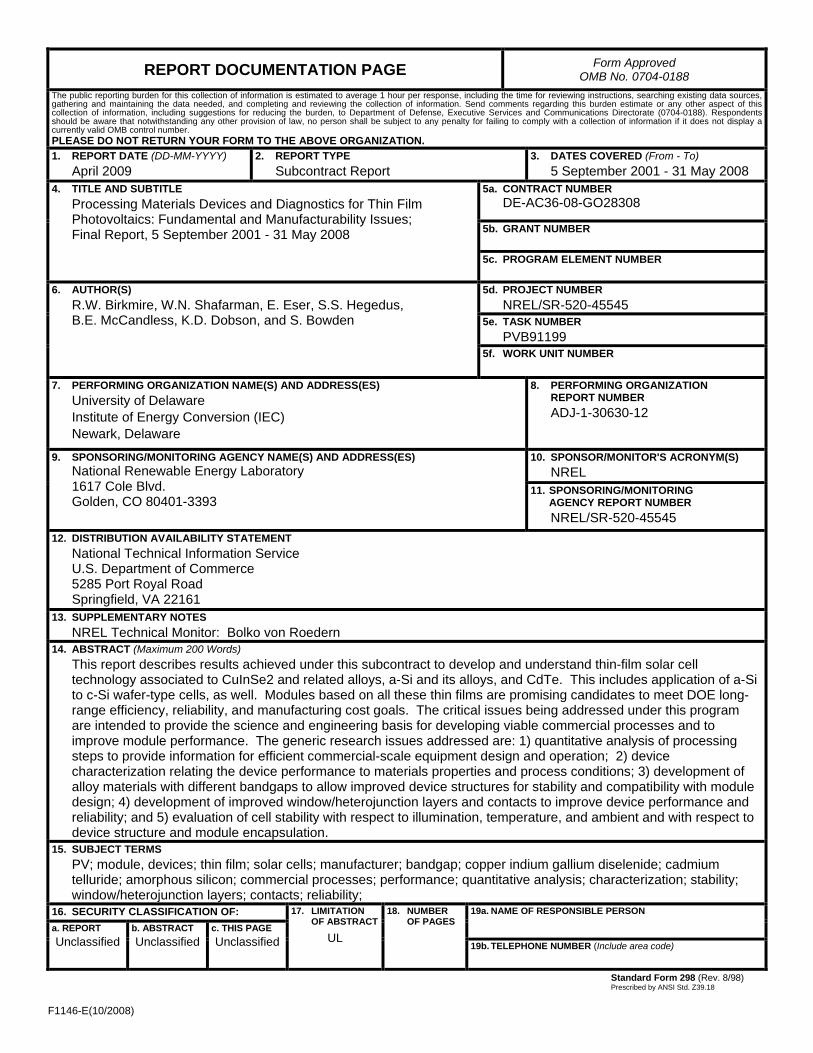
F1146-E(10/2008)
REPORT DOCUMENTATION PAGE Form Approved OMB No. 0704-0188
The public reporting burden for this collection of information is estimated to average 1 hour per response, including the time for reviewing instructions, searching existing data sources, gathering and maintaining the data needed, and completing and reviewing the collection of information. Send comments regarding this burden estimate or any other aspect of this collection of information, including suggestions for reducing the burden, to Department of Defense, Executive Services and Communications Directorate (0704-0188). Respondents should be aware that notwithstanding any other provision of law, no person shall be subject to any penalty for failing to comply with a collection of information if it does not display a currently valid OMB control number. PLEASE DO NOT RETURN YOUR FORM TO THE ABOVE ORGANIZATION. 1. REPORT DATE (DD-MM-YYYY)
April 2009 2. REPORT TYPE
Subcontract Report 3. DATES COVERED (From - To)
5 September 2001 - 31 May 2008 4. TITLE AND SUBTITLE
Processing Materials Devices and Diagnostics for Thin Film Photovoltaics: Fundamental and Manufacturability Issues; Final Report, 5 September 2001 - 31 May 2008
5a. CONTRACT NUMBER DE-AC36-08-GO28308
5b. GRANT NUMBER
5c. PROGRAM ELEMENT NUMBER
6. AUTHOR(S) R.W. Birkmire, W.N. Shafarman, E. Eser, S.S. Hegedus, B.E. McCandless, K.D. Dobson, and S. Bowden
5d. PROJECT NUMBER NREL/SR-520-45545
5e. TASK NUMBER PVB91199
5f. WORK UNIT NUMBER
7. PERFORMING ORGANIZATION NAME(S) AND ADDRESS(ES) University of Delaware Institute of Energy Conversion (IEC) Newark, Delaware
8. PERFORMING ORGANIZATION REPORT NUMBER ADJ-1-30630-12
9. SPONSORING/MONITORING AGENCY NAME(S) AND ADDRESS(ES) National Renewable Energy Laboratory 1617 Cole Blvd. Golden, CO 80401-3393
10. SPONSOR/MONITOR'S ACRONYM(S) NREL
11. SPONSORING/MONITORING AGENCY REPORT NUMBER NREL/SR-520-45545
12. DISTRIBUTION AVAILABILITY STATEMENT National Technical Information Service U.S. Department of Commerce 5285 Port Royal Road Springfield, VA 22161
13. SUPPLEMENTARY NOTES NREL Technical Monitor: Bolko von Roedern
14. ABSTRACT (Maximum 200 Words) This report describes results achieved under this subcontract to develop and understand thin-film solar cell technology associated to CuInSe2 and related alloys, a-Si and its alloys, and CdTe. This includes application of a-Si to c-Si wafer-type cells, as well. Modules based on all these thin films are promising candidates to meet DOE long-range efficiency, reliability, and manufacturing cost goals. The critical issues being addressed under this program are intended to provide the science and engineering basis for developing viable commercial processes and to improve module performance. The generic research issues addressed are: 1) quantitative analysis of processing steps to provide information for efficient commercial-scale equipment design and operation; 2) device characterization relating the device performance to materials properties and process conditions; 3) development of alloy materials with different bandgaps to allow improved device structures for stability and compatibility with module design; 4) development of improved window/heterojunction layers and contacts to improve device performance and reliability; and 5) evaluation of cell stability with respect to illumination, temperature, and ambient and with respect to device structure and module encapsulation.
15. SUBJECT TERMS PV; module, devices; thin film; solar cells; manufacturer; bandgap; copper indium gallium diselenide; cadmium telluride; amorphous silicon; commercial processes; performance; quantitative analysis; characterization; stability; window/heterojunction layers; contacts; reliability;
16. SECURITY CLASSIFICATION OF: 17. LIMITATION OF ABSTRACT
UL
18. NUMBER OF PAGES
19a. NAME OF RESPONSIBLE PERSON a. REPORT
Unclassified b. ABSTRACT Unclassified
c. THIS PAGE Unclassified 19b. TELEPHONE NUMBER (Include area code)
Standard Form 298 (Rev. 8/98) Prescribed by ANSI Std. Z39.18


![MASTER SUBCONTRACT Agreement - Swinerton … Subcontract... · Web viewMASTER SUBCONTRACT Agreement THIS MASTER SUBCONTRACT AGREEMENT (“MSA” or “Agreement”) is made this [date]](https://img.pdfslide.us/doc/110x75/5adb1e4d7f8b9ae1768e1acc/master-subcontract-agreement-swinerton-subcontractweb-viewmaster-subcontract.jpg)