Embed Size (px)
Citation preview
IEEE TRANSACTIONS ON VERY LARGE SCALE INTEGRATION (VLSI) SYSTEMS, VOL. 27, NO. 6, JUNE 2019 1239
Probing Assessment Framework and Evaluationof Antiprobing Solutions
Huanyu Wang , Student Member, IEEE, Qihang Shi , Member, IEEE, Domenic Forte , Senior Member, IEEE,and Mark M. Tehranipoor, Fellow, IEEE
Abstract— Probing attacks against integrated circuits hasbecome a serious concern, especially for security-critical applica-tions. With the help of modern circuit editing tools, an attackercould remove layers of materials and expose wires carryingsensitive on-chip assets, such as cryptographic keys and pro-prietary firmware, for probing. Most of the existing protectionmethods use an active shield that provides tamper-evident coversat the top-most metal layers to the circuitry below. However,they lack formal proofs of their effectiveness as some activeshields have already been circumvented by hackers. In thispaper, we investigate the problem of protection against front-sideprobing attacks and propose a framework to assess a design’svulnerabilities against probing attacks. Metrics are developed toevaluate the resilience of designs to bypass an attack and reroutethe attack, the two common techniques used to compromisean antiprobing mechanism. Exemplary assets from a system-on-chip layout are used to evaluate the proposed flow. Theresults show that long net and high layer wires are vulnerableto a probing attack equipped with high aspect ratio focused ionbeam. Meanwhile, nets that occupy small area on the chip areprobably compromised through rerouting shield wires. On theother hand, the multilayer internal orthogonal shield performsthe best among common shield structures.
Index Terms— Assessment, focused ion beam (FIB), hardwaresecurity, physical attack, probing attack.
I. INTRODUCTION
W ITH the rapid development of information technol-ogy and increasing reliance on electronic systems,
the risk of leaking security-critical information, such as per-sonal confidential information, commercial data, encryptionkeys, obfuscation keys, device configuration, and firmwarestored in integrated circuits (ICs), through software- andhardware-based attacks is higher than ever. Although counter-measures against software and noninvasive hardware attacks,e.g., side channel and fault injection attacks, have been widelyinvestigated, there is no efficient protection method againstphysical attacks.
Manuscript received September 27, 2018; revised December 21, 2018;accepted February 5, 2019. Date of publication April 12, 2019; date ofcurrent version May 22, 2019. This work was supported in part by NSFunder Project 1717392, in part by SRC under Task ID 2769.001, and in partby AFOSR MURI under Project FA9550-14-1-0351. (Corresponding author:Huanyu Wang.)
The authors are with the Department of Electrical and ComputerEngineering, University of Florida, Gainesville, FL 32611 USA(e-mail: [email protected]; [email protected]; [email protected];[email protected]).
Color versions of one or more of the figures in this paper are availableonline at http://ieeexplore.ieee.org.
Digital Object Identifier 10.1109/TVLSI.2019.2901449
Physical attacks could circumvent encryption processes byattacking their silicon implementations to extract sensitiveinformation from devices. Probing is one kind of physicalattacks whereby an attacker makes contact with the probesat signal wires in order to extract sensitive information [1].With the help of focused ion beam (FIB), a powerful circuitediting tool that can mill and deposit material with nanoscaleprecision, an attacker can also circumvent protection mech-anisms and reach wires carrying sensitive information [2].While FIB-based attacks are often considered to be restrictedto very well-equipped attackers, it is now possible to rentby time or buy a secondhand FIB at very low cost. Further-more, since failure analysis community continuously improvesFIB resolution, even modern nanoscale chips cannot avoidFIB-based probing attacks. Successful probing attacks havebeen reported on smartcards and microcontrollers in mobiledevices [3], [4], in which plaintexts, such as personal data,code format intellectual property (IP), or even encryption keys,were compromised [5].
In recent literature, various countermeasures, e.g., activeshield, analog shield, and t-private circuit, have been proposedto protect security-critical circuits against front-side probingattacks that occur from the passivation layer and through uppermetal layers. Active shield is the most common method, whichdetects milling by placing a dynamic signal carrying wire meshas a protective shield on the top most metal layer [6], [7].To detect the attack, a digital pattern is transmitted throughthe shield wires, and the received signals are compared withthe same pattern from the lower metal layer. If a mismatchat a comparator is detected, an alarm is triggered, whichresults in a security action such as the destruction of sensitiveinformation. Unfortunately, large area overhead and routingcongestion are imposed on the design by the active shield.Furthermore, as will be demonstrated in our evaluation, a highaspect ratio FIB and its circuit edit capability can circumventactive shields [3], [4]. Analog shield, which measures analogparameters of the shield mesh, such as capacitance and delayto detect the attack, can be an alternative approach to activeshield [8]. However, its main challenge is detection of the errordue to process variation and environmental noise in advancedtechnology nodes. Reference [9] proposed the t-private circuitapproach where a security-critical circuit is transformed so thatat least t + 1 probes are required within one clock cycle toextract one bit of information. Although the t-private circuitincreases the probing attack’s difficulty and time cost, its
1063-8210 © 2019 IEEE. Personal use is permitted, but republication/redistribution requires IEEE permission.See http://www.ieee.org/publications_standards/publications/rights/index.html for more information.
Authorized licensed use limited to: University of Florida. Downloaded on July 12,2021 at 19:42:39 UTC from IEEE Xplore. Restrictions apply.
1240 IEEE TRANSACTIONS ON VERY LARGE SCALE INTEGRATION (VLSI) SYSTEMS, VOL. 27, NO. 6, JUNE 2019
O(t2) times area overhead for design transformation is pro-hibitively expensive [10]. Furthermore, the randomized encod-ing/decoding bits used in t-private circuits are themselvesvulnerable to FIB-based tampering.
Even though back-side probing attacks, which occur throughthe silicon substrate rather than top-level passivation, havebeen proposed, security-critical designs may choose to fab-ricate a back-to-back 3-D IC to avoid leaving back-sideexposed [6]. Therefore, protection against front-side attacks isof prime importance. Among existing countermeasures againstfront-side probing attacks, shield-based approaches are themost investigated. However, there has never been a formalevaluation of their overall effectiveness, especially when thehigh aspect ratio FIB can easily bypass the shield protection.In addition, no existing literature has investigated as to whichrouting layer is the best place to build the shield and detecta breach. In fact, top routing layers are known to have muchwider minimum wire width and space than the lower layers,thus creating more chances for bypassing the shield withadvanced FIB. This is especially true for devices, such assmartcards, which are often fabricated with the technologyof larger dimensions such as 90 nm [3], [11].
In this paper, we make the following contributions:1) a framework to quantitatively assess the vulnerability
of a design’s layout against front-side probing attacks;2) an exposed area (EA) metric to assess the probing attack,
which utilizes the space between shield wires with highaspect ratio FIB, considering three probing scenarioswith different attack assumptions;
3) an added trace length metric to assess the probingattack, which reroutes shield wires to open a shield-freeregion;
4) a shield structure taxonomy that summarizes existingcommon shield patterns from the literature;
5) evaluations of the proposed methodology on multipleassets from a system-on-chip (SoC) benchmark underthe protection of different shield structures.
The rest of this paper is organized as follows. Section IIpresents a background related to probing attack and protection.Section III presents the proposed framework, and the metricsto assess bypass attack and reroute attack. In Section IV,we provide evaluation results on the proposed methodologyusing a SoC benchmark, before concluding the paper inSection V.
II. BACKGROUND
A number of techniques can be used to extract data fromdevices. One example is photon emission analysis where thephotons emitted from the switching transistors are measuredand analyzed, but the resolution is limited by the wavelengthof infrared light (∼1 µm) [12]. A modern optical and electronmicroscopy can be used to extract the information stored inread-only memory (ROM) by observing the binary state ofeach cell. However, they are not applied to electrically erasableprogrammable ROM or flash memory because the electrondistribution might be changed and thus the contents insidethe memory will be disturbed [13]. Probing is another kindof physical attack, which is particularly effective for dataextraction and hence warrant attention and investigation.
A. Probing TechniquesCircuit probing refers to techniques that allow an attacker
to directly observe partial or full sensitive information,e.g., plaintexts or encryption keys in a chip. Signals that aremore likely to be targeted in a probing attack are termedas assets. An asset is a resource of value which is worthprotecting from an adversary. Probing attacks are categorizedas invasive attacks because they require decapsulation, expo-sure of signal routing, and permanent modification of theIC. Typical probing attacks [4], [10] consist of the followingsteps.
The first step of the most invasive physical attacks is toeither partially or fully remove the chip package in orderto expose the silicon die. If the attacker does not possessthe layout and/or original netlist, then full or partial reverseengineering may be needed to understand how the chip works.By studying the netlist, the attacker can identify the assetssuch as encryption keys, device configuration, manufacturerfirmware, and obfuscation keys. One-to-one correspondencebetween the netlist and the layout can then determine the wiresand buses to be probed as well as their exact locations, and inthe event where cutting of a wire is unavoidable, determiningwhether the cut would impact asset extraction. The next stepis locating these wires and buses in the IC sample under attackusing the coordinates achieved from sacrificial devices. Somecomputer-aided design (CAD) tools, such as the SynopsysCamelot CAD Navigation System, could help to accuratelylocate and reach the target wires in the chip at nanoscaleprecision. An overlay of CAD layout database/graphic datasystem layout data can be shown in a scanning electronmicroscope or a FIB live image. Overlay of images fromother inspection techniques, e.g., photon-emission electronmicroscopy, can also be used for navigation.
Wires of targeted nets that the attacker wishes to reach arelikely buried under multiple passivation, metal, and dielectriclayers. On ICs fabricated with feature dimensions larger than0.35 µm, laser cutters can be used to remove these layersto expose targeted wires for probing [1]. For technologiesof lower dimensions, the most common and powerful toolis FIB [13]. With the help of a modern FIB system, suchas ZEISS ORION NanoFab [14], an attacker can edit outobstructing circuitry with 5 nm level resolution [2]. The betterthe resolution of the FIB system, the higher the FIB aspectratio it can achieve, and the smaller the milling hole it willcreate. Typical FIB systems use a gallium ion (Ga+) beamhaving spot size less than 10 nm. However, it is difficultto control the Ga ions in 10 nm level precision due to therelatively large mass of Ga+. Thus, the effective operationalresolution for Ga-FIB is sub-100 nm. Recently, a helium ion(He+) beam FIB system is available [14], which is capablefor nanostructuring in 5 nm level resolution [15]. However,because of the smaller mass of He+, the sputter rate of He-FIBis much slower than Ga-FIB.
Using FIB, a small hole can be milled in the chip to exposetarget wires from the lower layer as shown in Fig. 1(a).This feature indicates that many countermeasures can bedisabled by simply disconnecting a few wires, and that aFIB-equipped attacker could field as many concurrent probes
Authorized licensed use limited to: University of Florida. Downloaded on July 12,2021 at 19:42:39 UTC from IEEE Xplore. Restrictions apply.
WANG et al.: PROBING ASSESSMENT FRAMEWORK AND EVALUATION OF ANTIPROBING SOLUTIONS 1241
Fig. 1. (a) FIB deposits Pt in the milling hole to build conducting path fromtarget wire. (b) Deposited conducting path serves as electrical probe contact.
Fig. 2. Basic working principle of active shield and bypass attack on activeshield.
as a logic analyzer allows. State-of-the-art FIBs can alsodeposit material in the milling hole with nanometer resolution.Platinum (Pt) or tungsten (W) gas is released from the gasinjection system (GIS) nozzle at the chip surface. A high-energy ion beam can help these gas atoms to be deposited inthe milling hole to build a conducting path that can serve aselectrical probe contacts as shown in Fig. 1(b). When the targetwire is exposed and an electrical connection is establishedwithout triggering any probing alarm from active or analogshields, the asset signals can be extracted, for example, witha nano or microprobing system.
B. Countermeasures and Limitations
In this section, we briefly review FIB/probing countermea-sures and highlight their limitations. Unfortunately, to the bestof our knowledge, no method has been proposed to adequatelyaddress back-side probing attacks, which is a part of our futurework.
Active shield is so far the most widely used probing coun-termeasure. In this approach, a shield, which carries signals,is placed on the top-most metal layer to detect holes milled byFIB. As shown in Fig. 2, a digital pattern is generated froma pattern generator, transmitted through the shield wires onthe top-most metal layer, and it is then compared with a copyof itself transmitted from the lower layer. If an attacker mills
Fig. 3. Probe attempt detector.
through the shield wires on the top layer to reach the lowertarget wire, a hole is expected to cut one or more shield wires,thereby leading to a mismatch at the comparator and triggeringan alarm signal to erase or stop the generation of sensitiveinformation. Despite its popularity, the biggest problem foractive shield is that they impose large design overheads andare very vulnerable to attacks with advanced FIBs. Aspectratio is a measure of the FIB performance defined as theratio between depth and diameter of the milled hole [16].A FIB with high aspect ratio can penetrate the shield witha hole of smaller diameter by leveraging the space betweenshield wires without damaging the shield wires, which is calledbypass attack. In addition to milling, FIB is also capable ofdepositing conducting traces [17], which adds circuit editingto the attacker’s capability. This capability allows the attackerto implement reroute attack which makes the shield wire freeof cutting by rerouting a copy path between identified equipo-tential points. Reroute attack is a good alternative techniquewhen it proves too difficult to bypass [3], [4]. The attackercan also completely disable the active shield by editing itscontrol circuitry or payload. When milling and depositing innanometer scale and applied on silicon ICs, the state-of-artFIB systems can reach an aspect ratio up to ∼10 [18]. Anotherproblem with the active shield method is that at least an entiremetal routing layer must be dedicated to the shield, which doesnot go well with the designs with tight cost margin, or designswith few routing layers.
An alternative approach to active shield is to constructan analog shield. Instead of generating, transmitting, andcomparing digital patterns, analog shields monitor parametricdisturbances, such as capacitance, RC delay, with its meshwires. In addition to shield designs, the probe attempt detector(PAD) [8] (as shown in Fig. 3) also uses capacitance measure-ment on selected security-critical wires to detect additionalcapacitance introduced by a metal probe. Compared to activeshields, analog shields detect probing without test patterns andrequire a smaller area overhead. The PAD technique is alsounique in remaining effective against electrical probing fromthe back-side. The problem with analog sensors or shieldsis that analog measurements are less reliable due to process
Authorized licensed use limited to: University of Florida. Downloaded on July 12,2021 at 19:42:39 UTC from IEEE Xplore. Restrictions apply.
1242 IEEE TRANSACTIONS ON VERY LARGE SCALE INTEGRATION (VLSI) SYSTEMS, VOL. 27, NO. 6, JUNE 2019
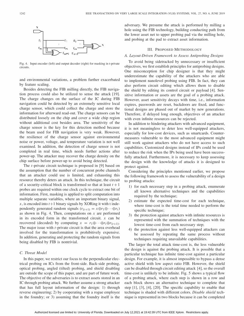
Fig. 4. Input encoder (left) and output decoder (right) for masking in t-privatecircuits.
and environmental variations, a problem further exacerbatedby feature scaling.
Besides detecting the FIB milling directly, the FIB naviga-tion process could also be utilized to sense the attack [19].The charge changes on the surface of the IC during FIBnavigation could be detected by an extremely sensitive localcharge sensor, which could collect the charge and store theinformation for afterward read-out. The charge sensors can bedistributed loosely on the chip and cover a wide chip regionwithout additional cost besides area. The sensitivity of thecharge sensor is the key for this detection method becausethe beam used for FIB navigation is very weak. However,the resilience of the charge sensor against environmentalnoise or power, voltage, and temperature variation is not wellexamined. In addition, the detection of charge sensor is notcompleted in real time, which needs further actions afterpower-up. The attacker may recover the charge density on thechip surface before power-up to avoid being detected.
The t-private circuit technique is proposed in [9] based onthe assumption that the number of concurrent probe channelsthat an attacker could use is limited, and exhausting thisresource thereby deters an attack. In this technique, the circuitof a security-critical block is transformed so that at least t + 1probes are required within one clock cycle to extract one bit ofinformation. First, masking is applied to split computation intomultiple separate variables, where an important binary signal,x , is encoded into t+1 binary signals by XORing it with t inde-pendently generated random signals (r(t+1) = x⊕r1⊕· · ·⊕rt )as shown in Fig. 4. Then, computations on x are performedin its encoded form in the transformed circuit. x can berecovered (decoded) by computing x = r1⊕· · ·⊕rt⊕r(t+1).The major issue with t-private circuit is that the area overheadinvolved for the transformation is prohibitively expensive.In addition, generating and protecting the random signals frombeing disabled by FIB is nontrivial.
C. Threat Model
In this paper, we restrict our focus to the perpendicular elec-trical probing on ICs from the front-side. Back-side probing,optical probing, angled (tilted) probing, and shield disablingare outside the scope of this paper, and are part of future work.The objective of the adversaries is to extract assets stored in anIC through probing attack. We further assume a strong attackerthat has full layout information of the design: 1) throughreverse engineering; 2) by cooperating with a rogue employeein the foundry; or 3) assuming that the foundry itself is the
adversary. We presume the attack is performed by milling ahole using the FIB technology, building conducting path fromthe lower asset net to upper probing pad via the milling hole,and probing at the pad to extract asset information.
III. PROPOSED METHODOLOGY
A. Layout-Driven Framework to Assess Antiprobing Designs
To avoid being sidetracked by unnecessary or insufficientobjectives, we first establish principles for antiprobing designs.One misconception for chip designer is that they mightunderestimate the capability of the attackers who are ableto implement nanolevel probing using FIB. In fact, they canalso perform circuit editing which allows them to disablethe shield by editing its control circuit or payload [4]. Sen-sitive information or assets are the goal of a probing attack.However, asset sensitivity decays with time, i.e., informationexpires, passwords are reset, backdoors are fixed, and func-tional designs are phased out of market by new generations.Therefore, if delayed long enough, objectives of an attackerwith even infinite resources can be rejected.
In addition to hindering attackers with advanced equipment,it is not meaningless to deter less well-equipped attackers,especially for low-cost devices, such as smartcards. Counter-measures vulnerable to the most advanced equipment mightstill work against attackers who do not have access to suchcapabilities. Customized designs instead of IPs could be usedto reduce the risk when the IPs being used have been success-fully attacked. Furthermore, it is necessary to keep assessingthe design with the knowledge of attacks it is designed toprotect against.
Considering the principles mentioned earlier, we proposethe following framework to assess the vulnerability of a designto probing attacks:
1) for each necessary step in a probing attack, enumerateall known alternative techniques and the capabilitiesrequired by the technique;
2) estimate the expected time-cost for each technique,where time-cost is the total time needed to perform thespecific technique;
3) the protection against attackers with infinite resources isrepresented with the summation of techniques with thelowest time-cost from each necessary step;
4) the protection against less well-equipped attackers canbe assessed by repeating the same process withouttechniques requiring unavailable capabilities.
The larger the total attack time-cost is, the less vulnerablethe design is against the probing attack. It is possible that aparticular technique has infinite time-cost against a particulardesign. For example, it is almost impossible to bypass a denseactive shield with low aspect ratio FIB. However, the shieldcan be disabled through circuit editing attack [4], so the overalltime-cost is unlikely to be infinite. Fig. 5 shows a typical flowof a probing attack, where each step is shown in a row andeach block shows an alternative technique to complete thatstep [1], [3], [4], [20]. The specific capability to enable thattechnique is shaded with different colors. Disable shield tech-nique is represented in two blocks because it can be completed
Authorized licensed use limited to: University of Florida. Downloaded on July 12,2021 at 19:42:39 UTC from IEEE Xplore. Restrictions apply.
WANG et al.: PROBING ASSESSMENT FRAMEWORK AND EVALUATION OF ANTIPROBING SOLUTIONS 1243
Fig. 5. Diagram of known microprobing techniques for assessment of designvulnerability.
Fig. 6. Inputs and outputs for the assessment of bypass attack and rerouteattack.
either by circuit editing or fault injection, but in both optionsreverse engineering is required. Techniques in white boxesthat do not have a colored alternative show possible exploitsfrom design flaws rather than lack of protection. For example,“use shield to help fine navigation” is possible if shield wireswere placed in the same direction with regard to functionalrouting [4], and if no internal clock source is used, the attackercould simply “stop external clock” to extract all informationwithout having to use multiple simultaneous probes.
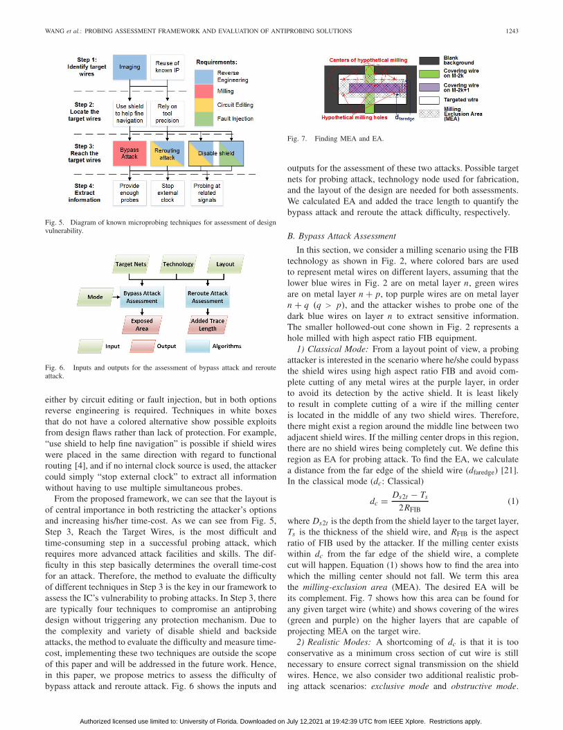
From the proposed framework, we can see that the layout isof central importance in both restricting the attacker’s optionsand increasing his/her time-cost. As we can see from Fig. 5,Step 3, Reach the Target Wires, is the most difficult andtime-consuming step in a successful probing attack, whichrequires more advanced attack facilities and skills. The dif-ficulty in this step basically determines the overall time-costfor an attack. Therefore, the method to evaluate the difficultyof different techniques in Step 3 is the key in our framework toassess the IC’s vulnerability to probing attacks. In Step 3, thereare typically four techniques to compromise an antiprobingdesign without triggering any protection mechanism. Due tothe complexity and variety of disable shield and backsideattacks, the method to evaluate the difficulty and measure time-cost, implementing these two techniques are outside the scopeof this paper and will be addressed in the future work. Hence,in this paper, we propose metrics to assess the difficulty ofbypass attack and reroute attack. Fig. 6 shows the inputs and
Fig. 7. Finding MEA and EA.
outputs for the assessment of these two attacks. Possible targetnets for probing attack, technology node used for fabrication,and the layout of the design are needed for both assessments.We calculated EA and added the trace length to quantify thebypass attack and reroute the attack difficulty, respectively.
B. Bypass Attack Assessment
In this section, we consider a milling scenario using the FIBtechnology as shown in Fig. 2, where colored bars are usedto represent metal wires on different layers, assuming that thelower blue wires in Fig. 2 are on metal layer n, green wiresare on metal layer n + p, top purple wires are on metal layern + q (q > p), and the attacker wishes to probe one of thedark blue wires on layer n to extract sensitive information.The smaller hollowed-out cone shown in Fig. 2 represents ahole milled with high aspect ratio FIB equipment.
1) Classical Mode: From a layout point of view, a probingattacker is interested in the scenario where he/she could bypassthe shield wires using high aspect ratio FIB and avoid com-plete cutting of any metal wires at the purple layer, in orderto avoid its detection by the active shield. It is least likelyto result in complete cutting of a wire if the milling centeris located in the middle of any two shield wires. Therefore,there might exist a region around the middle line between twoadjacent shield wires. If the milling center drops in this region,there are no shield wires being completely cut. We define thisregion as EA for probing attack. To find the EA, we calculatea distance from the far edge of the shield wire (dfaredge) [21].In the classical mode (dc: Classical)
dc = Ds2t − Ts
2RFIB(1)
where Ds2t is the depth from the shield layer to the target layer,Ts is the thickness of the shield wire, and RFIB is the aspectratio of FIB used by the attacker. If the milling center existswithin dc from the far edge of the shield wire, a completecut will happen. Equation (1) shows how to find the area intowhich the milling center should not fall. We term this areathe milling-exclusion area (MEA). The desired EA will beits complement. Fig. 7 shows how this area can be found forany given target wire (white) and shows covering of the wires(green and purple) on the higher layers that are capable ofprojecting MEA on the target wire.
2) Realistic Modes: A shortcoming of dc is that it is tooconservative as a minimum cross section of cut wire is stillnecessary to ensure correct signal transmission on the shieldwires. Hence, we also consider two additional realistic prob-ing attack scenarios: exclusive mode and obstructive mode.
Authorized licensed use limited to: University of Florida. Downloaded on July 12,2021 at 19:42:39 UTC from IEEE Xplore. Restrictions apply.
1244 IEEE TRANSACTIONS ON VERY LARGE SCALE INTEGRATION (VLSI) SYSTEMS, VOL. 27, NO. 6, JUNE 2019
Fig. 8. (a) Accessing target wires without cutting any shield wires (exclusivemode). (b) Accessing target wires with a part of the shield wire being cut off(obstructive mode).
Both modes can access probing target wires successfully, but ata different time-cost, and have different scope of applications.The exclusive mode probing is applicable for both active shieldand analog shield designs, while the obstructive mode probingis only applicable for analog shield design.
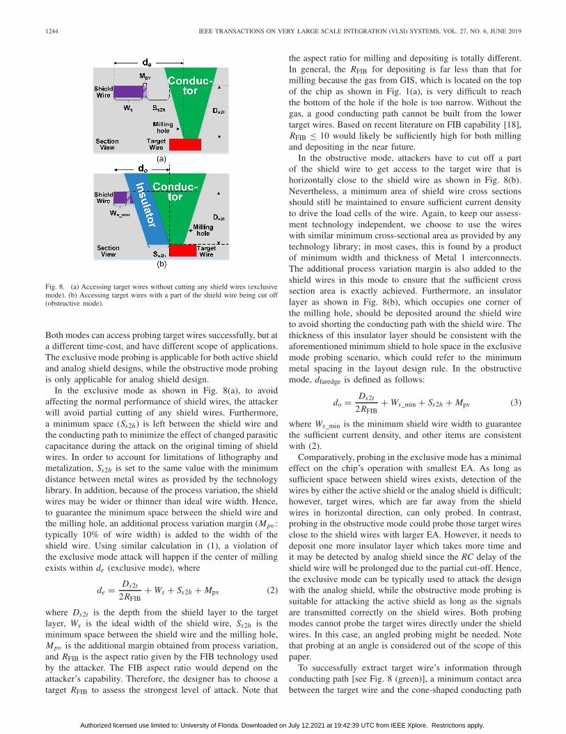
In the exclusive mode as shown in Fig. 8(a), to avoidaffecting the normal performance of shield wires, the attackerwill avoid partial cutting of any shield wires. Furthermore,a minimum space (Ss2h) is left between the shield wire andthe conducting path to minimize the effect of changed parasiticcapacitance during the attack on the original timing of shieldwires. In order to account for limitations of lithography andmetalization, Ss2h is set to the same value with the minimumdistance between metal wires as provided by the technologylibrary. In addition, because of the process variation, the shieldwires may be wider or thinner than ideal wire width. Hence,to guarantee the minimum space between the shield wire andthe milling hole, an additional process variation margin (Mpv :typically 10% of wire width) is added to the width of theshield wire. Using similar calculation in (1), a violation ofthe exclusive mode attack will happen if the center of millingexists within de (exclusive mode), where
de = Ds2t
2RFIB+ Ws + Ss2h + Mpv (2)
where Ds2t is the depth from the shield layer to the targetlayer, Ws is the ideal width of the shield wire, Ss2h is theminimum space between the shield wire and the milling hole,Mpv is the additional margin obtained from process variation,and RFIB is the aspect ratio given by the FIB technology usedby the attacker. The FIB aspect ratio would depend on theattacker’s capability. Therefore, the designer has to choose atarget RFIB to assess the strongest level of attack. Note that
the aspect ratio for milling and depositing is totally different.In general, the RFIB for depositing is far less than that formilling because the gas from GIS, which is located on the topof the chip as shown in Fig. 1(a), is very difficult to reachthe bottom of the hole if the hole is too narrow. Without thegas, a good conducting path cannot be built from the lowertarget wires. Based on recent literature on FIB capability [18],RFIB ≤ 10 would likely be sufficiently high for both millingand depositing in the near future.
In the obstructive mode, attackers have to cut off a partof the shield wire to get access to the target wire that ishorizontally close to the shield wire as shown in Fig. 8(b).Nevertheless, a minimum area of shield wire cross sectionsshould still be maintained to ensure sufficient current densityto drive the load cells of the wire. Again, to keep our assess-ment technology independent, we choose to use the wireswith similar minimum cross-sectional area as provided by anytechnology library; in most cases, this is found by a productof minimum width and thickness of Metal 1 interconnects.The additional process variation margin is also added to theshield wires in this mode to ensure that the sufficient crosssection area is exactly achieved. Furthermore, an insulatorlayer as shown in Fig. 8(b), which occupies one corner ofthe milling hole, should be deposited around the shield wireto avoid shorting the conducting path with the shield wire. Thethickness of this insulator layer should be consistent with theaforementioned minimum shield to hole space in the exclusivemode probing scenario, which could refer to the minimummetal spacing in the layout design rule. In the obstructivemode, dfaredge is defined as follows:
do = Ds2t
2RFIB+ Ws_min + Ss2h + Mpv (3)
where Ws_min is the minimum shield wire width to guaranteethe sufficient current density, and other items are consistentwith (2).
Comparatively, probing in the exclusive mode has a minimaleffect on the chip’s operation with smallest EA. As long assufficient space between shield wires exists, detection of thewires by either the active shield or the analog shield is difficult;however, target wires, which are far away from the shieldwires in horizontal direction, can only probed. In contrast,probing in the obstructive mode could probe those target wiresclose to the shield wires with larger EA. However, it needs todeposit one more insulator layer which takes more time andit may be detected by analog shield since the RC delay of theshield wire will be prolonged due to the partial cut-off. Hence,the exclusive mode can be typically used to attack the designwith the analog shield, while the obstructive mode probing issuitable for attacking the active shield as long as the signalsare transmitted correctly on the shield wires. Both probingmodes cannot probe the target wires directly under the shieldwires. In this case, an angled probing might be needed. Notethat probing at an angle is considered out of the scope of thispaper.
To successfully extract target wire’s information throughconducting path [see Fig. 8 (green)], a minimum contact areabetween the target wire and the cone-shaped conducting path
Authorized licensed use limited to: University of Florida. Downloaded on July 12,2021 at 19:42:39 UTC from IEEE Xplore. Restrictions apply.
WANG et al.: PROBING ASSESSMENT FRAMEWORK AND EVALUATION OF ANTIPROBING SOLUTIONS 1245
Algorithm 1 Proposed Locator Algorithm for EA.Input: targeted_nets, precision, all_layersOutput: draw.script
1 begin2 targeted_wire_shapes ⇐ get_net_shapes(targeted_nets)3 N ⇐ sizeof_collection(targeted_wire_shapes)4 for (i = 1 : N) do5 targeted_wire_shape ⇐ targeted_wire_shapes(i )6 canvas_size ⇐ get_sizes(get_bounding_box7 (targeted_wire_shape))*precision8 Print command in draw.script to create canvas in
draw.script whose size equals to canvas_size9 layers_above ⇐ get_layers_above(all_layers,
get_layerof(targeted_wire_shape))10 M ⇐ sizeof_collection(layers_above)11 for ( j = 1 : M) do12 this_layer ⇐ layers_above( j )13 d_faredge_on_thislayer ⇐ d_faredge (Classical,
Exclusive, or Obstructive)14 intersecting_wire_shapes ⇐
get_net_shapes(targeted_nets) inget_bounding_box(targeted_wire_shape) onthis_layer
15 L ⇐ sizeof_collection(intersecting_wire_shapes)16 for (k = 1 : L) do17 intersecting_wire_shape ⇐
intersecting_wire_shapes(k)18 Print command in draw.script to create
projection in draw.script whose radius/widthsequals to d_faredge_on_thislayer
19 end20 end21 end22 end
should be satisfied to guarantee the sufficient current densitythrough the conducting path. The cross section area of Metal 1in a technology can be used to determine this minimum contactarea. If the area of a continuous EA is smaller than theminimum contact area, this EA should also not be taken asa vulnerable area to probing attack since it cannot support agood signal transmission from target wire to external probestation.
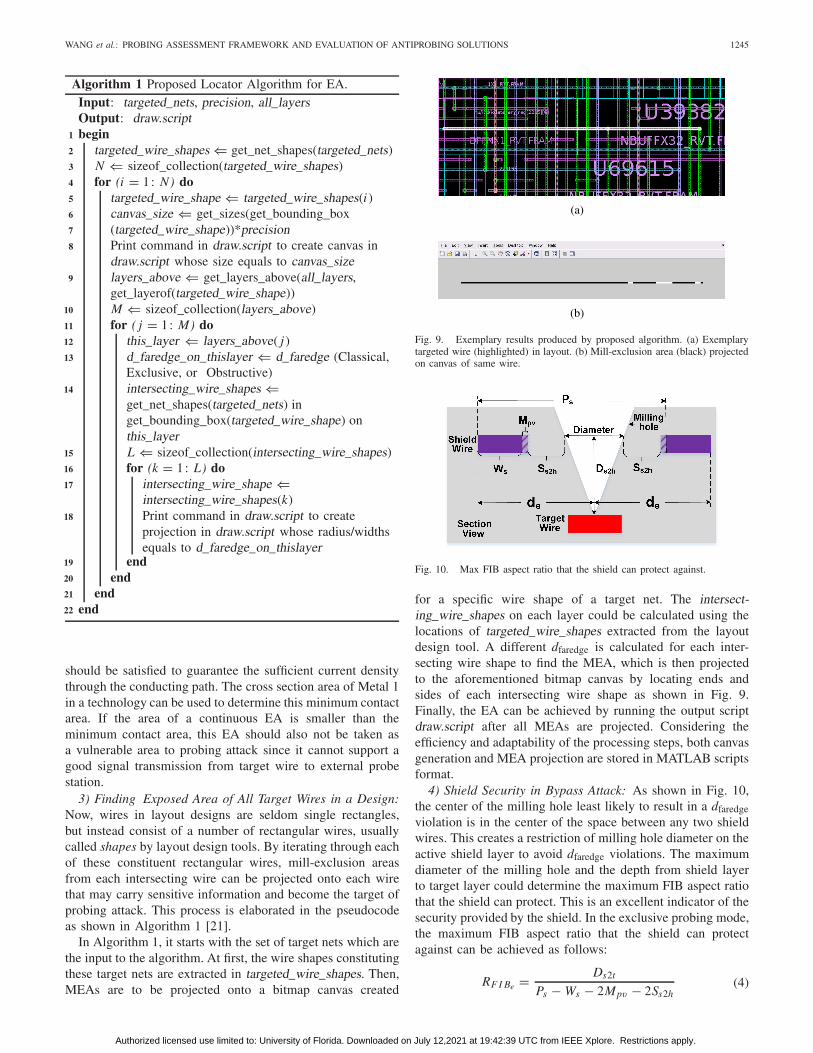
3) Finding Exposed Area of All Target Wires in a Design:Now, wires in layout designs are seldom single rectangles,but instead consist of a number of rectangular wires, usuallycalled shapes by layout design tools. By iterating through eachof these constituent rectangular wires, mill-exclusion areasfrom each intersecting wire can be projected onto each wirethat may carry sensitive information and become the target ofprobing attack. This process is elaborated in the pseudocodeas shown in Algorithm 1 [21].
In Algorithm 1, it starts with the set of target nets which arethe input to the algorithm. At first, the wire shapes constitutingthese target nets are extracted in targeted_wire_shapes. Then,MEAs are to be projected onto a bitmap canvas created
Fig. 9. Exemplary results produced by proposed algorithm. (a) Exemplarytargeted wire (highlighted) in layout. (b) Mill-exclusion area (black) projectedon canvas of same wire.
Fig. 10. Max FIB aspect ratio that the shield can protect against.
for a specific wire shape of a target net. The intersect-ing_wire_shapes on each layer could be calculated using thelocations of targeted_wire_shapes extracted from the layoutdesign tool. A different dfaredge is calculated for each inter-secting wire shape to find the MEA, which is then projectedto the aforementioned bitmap canvas by locating ends andsides of each intersecting wire shape as shown in Fig. 9.Finally, the EA can be achieved by running the output scriptdraw.script after all MEAs are projected. Considering theefficiency and adaptability of the processing steps, both canvasgeneration and MEA projection are stored in MATLAB scriptsformat.
4) Shield Security in Bypass Attack: As shown in Fig. 10,the center of the milling hole least likely to result in a dfaredgeviolation is in the center of the space between any two shieldwires. This creates a restriction of milling hole diameter on theactive shield layer to avoid dfaredge violations. The maximumdiameter of the milling hole and the depth from shield layerto target layer could determine the maximum FIB aspect ratiothat the shield can protect. This is an excellent indicator of thesecurity provided by the shield. In the exclusive probing mode,the maximum FIB aspect ratio that the shield can protectagainst can be achieved as follows:
RF I Be = Ds2t
Ps − Ws − 2Mpv − 2Ss2h(4)
Authorized licensed use limited to: University of Florida. Downloaded on July 12,2021 at 19:42:39 UTC from IEEE Xplore. Restrictions apply.
1246 IEEE TRANSACTIONS ON VERY LARGE SCALE INTEGRATION (VLSI) SYSTEMS, VOL. 27, NO. 6, JUNE 2019
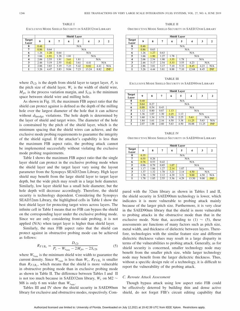
TABLE I
EXCLUSIVE MODE SHIELD SECURITY IN SAED32NM LIBRARY
where Ds2t is the depth from shield layer to target layer, Ps isthe pitch size of shield layer, Ws is the width of shield wire,Mpv is the process variation margin, and Ss2h is the minimumspace between shield wire and milling hole.
As shown in Fig. 10, the maximum FIB aspect ratio that theshield can protect against is defined as the depth of the millinghole over the largest diameter of the hole that it can achievewithout dfaredge violations. The hole depth is determined bythe layer of shield and target wires. The diameter of the holeis constrained by the pitch of the shield layer, which is theminimum spacing that the shield wires can achieve, and theexclusive mode probing requirements to guarantee the integrityof the shield signal. If the attacker’s capability is less thanthe maximum FIB aspect ratio, the probing attack cannotbe implemented successfully without violating the exclusivemode probing requirements.
Table I shows the maximum FIB aspect ratio that the singlelayer shield can protect in the exclusive probing mode whenthe shield layer and the target layer vary using the layoutparameter from the Synopsys SEAD32nm Library. High layershield may benefit from the large shield layer to target layerdepth, but the wide pitch may result in a large hole diameter.Similarly, low layer shield has a small hole diameter, but thehole depth will decrease accordingly. Therefore, the shieldsecurity is technology dependent. Considering the SynopsysSEAD32nm Library, the highlighted cells in Table I show thebest shield layer for protecting target wires across layers. Theinfinite cell in Table I means that no FIB can bypass the shieldon the corresponding layer under the exclusive probing mode.Since we are only considering front-side probing, it is notapplied (N/A) when target layer is higher than shield layer.
Similarly, the max FIB aspect ratio that the shield canprotect against in obstructive probing mode can be achievedas follows:
RF I Bo = Ds2t
Ps − Wsmin − 2Mpv − 2Ss2h(5)
where Wsmin is the minimum shield wire width to guarantee thecurrent density. Since Wsmin is less than Ws , RF I Bo is smallerthan RF I Be , which means that the shield is more vulnerablein obstructive probing mode than in exclusive probing modeas shown in Table II. The difference between Tables I and IIis not too much because in SAED32nm library, Ws on M2 ∼M8 is only 6 nm wider than Wsmin .
Tables III and IV show the shield security in SAED90nmlibrary for exclusive and obstructive modes, respectively. Com-
TABLE II
OBSTRUCTIVE MODE SHIELD SECURITY IN SAED32NM LIBRARY
TABLE III
EXCLUSIVE MODE SHIELD SECURITY IN SAED90NM LIBRARY
TABLE IV
OBSTRUCTIVE MODE SHIELD SECURITY IN SAED90NM LIBRARY
pared with the 32nm library as shown in Tables I and II,the shield security in SAED90nm technology is lower, whichindicates it is more vulnerable to probing attack mainlybecause of the larger pitch size. Furthermore, it is very clearin the SAED90nm library that the shield is more vulnerableto probing attacks in the obstructive mode than that in theexclusive mode. Note that, according to (1) ∼ (5), theseassessments are functions of many factors such as pitch size,metal width, and thickness of dielectric between layers. There-fore, technologies with the similar feature size and differentdielectric thickness values may result in a large disparity interms of the vulnerabilities to probing attack. Generally, as forshield security is concerned, smaller technology node maybenefit from the smaller pitch size, while larger technologynode may benefit from the larger dielectric thickness. Thus,without a specific design rule of a technology, it is difficult toreport the vulnerability of the probing attack.
C. Reroute Attack Assessment
Though bypass attack using low aspect ratio FIB couldbe effectively deterred by building thin and dense activeshield, do not forget FIB’s circuit editing capability that
Authorized licensed use limited to: University of Florida. Downloaded on July 12,2021 at 19:42:39 UTC from IEEE Xplore. Restrictions apply.
WANG et al.: PROBING ASSESSMENT FRAMEWORK AND EVALUATION OF ANTIPROBING SOLUTIONS 1247
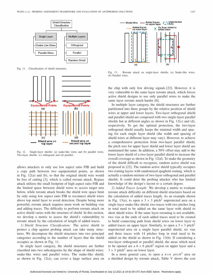
Fig. 11. Classification of shield structures.
Fig. 12. Single-layer shields: (a) snake-like wires and (b) parallel wires.Two-layer shields: (c) orthogonal and (d) parallel.
allows attackers to only use low aspect ratio FIB and builda copy path between two equipotential points, as shownin Fig. 12(a) and (b), so that the original shield wire wouldbe free of cutting [3], which is called reroute attack. Bypassattack utilizes the small footprint of high aspect ratio FIB andthe limited space between shield wires to access target netsbelow, while reroute attack breaks the shield wire space limitby only using low aspect ratio FIB to reconnect shield wiresabove top metal layer to avoid detection. Despite being morepowerful, reroute attack requires more work on building viasand adding traces. The difficulty to perform reroute attack onactive shield varies with the structure of shield. In this section,we develop a metric to assess the shield’s vulnerability toreroute attack by the calculation of length of added traces.
1) Shield Structure Classification: The active shield toprotect a chip against probing attack can take many struc-tures. We decompose the shield structures into two principalcategories according to the number of layers that the shieldoccupies as shown in Fig. 11.
In single layer category, the shield structures are furtherclassified into two subcategories by the shape of shield wires:snake-like wires and parallel wires. The snake-like shield,as shown in Fig. 12(a), can cover a large surface area on
Fig. 13. Reroute attack on single-layer shields. (a) Snake-like wires.(b) Parallel wires.
the chip with only few driving signals [22]. However, it isvery vulnerable to the same layer reroute attack, which forcesactive shield designs to use only parallel wires to make thesame layer reroute much harder [6].
In multiple layer category, the shield structures are furtherpartitioned into three groups by the relative position of shieldwires at upper and lower layers. Two-layer orthogonal shieldand parallel shield are composed with two single-layer parallelshields but at different angles as shown in Fig. 12(c) and (d),respectively. To get the optimal protection, the two-layerorthogonal shield usually keeps the minimal width and spac-ing for each single layer shield (the width and spacing ofshield wires at different layer may vary). However, to achievea comprehensive protection from two-layer parallel shield,the pitch size for upper layer shield and lower layer shield aremaintained the same. In addition, a 50% offset may add to thelower layer shield of a two-layer parallel shield to increase theoverall coverage as shown in Fig. 12(d). To make the geometryof the shield difficult to recognize, random active shield wasproposed in [22]. The random active shield typically occupiestwo routing layers with randomized spaghetti routing, which isactually a random mixture of two-layer orthogonal and parallelshields. It could deter the probing attacker who has limitedknowledge of the design’s layout to a certain degree.
2) Added Traces Length: We develop a metric to evaluatereroute attack difficulty on different shield structures based onthe calculation of added traces length. As an example shownin Fig. 13(a), to open a 3 × 3 pitch2 unprotected area on asingle layer snake-like shield, two traces with two pitches longin total need to be added on the same layer with shield toshort shield wires. If the same layer rerouting is not available,two vias at the ends of each added traces need to be createdto build connecting path from shield wires on lower layer toadded traces on upper layer. Similarly, to open a 3 × 3 pitch2
unprotected area on a single layer parallel shield, six viasand three traces with 14 pitches long in total need to beadded on the shield as shown in Fig. 13(b). If considering atwo-layer orthogonal or parallel shield, the areas which needto be opened are a 6 × 6 pitch2 region on upper layer and a3 × 3 pitch2 area on lower layer.
In a more general case, to open a n×n pi tch2 area ona shielded design by reroute attack, Table V shows the cost
Authorized licensed use limited to: University of Florida. Downloaded on July 12,2021 at 19:42:39 UTC from IEEE Xplore. Restrictions apply.
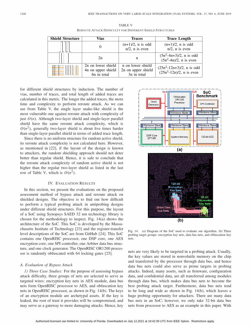
1248 IEEE TRANSACTIONS ON VERY LARGE SCALE INTEGRATION (VLSI) SYSTEMS, VOL. 27, NO. 6, JUNE 2019
TABLE V
REROUTE ATTACK DIFFICULTY FOR DIFFERENT SHIELD STRUCTURES
for different shield structures by induction. The number ofvias, number of traces, and total length of added traces arecalculated in this metric. The longer the added traces, the moretime and complexity to perform reroute attack. As we cansee from Table V, the single layer snake-like shield is themost vulnerable one against reroute attack with complexity ofjust O(n). Although two-layer shield and single-layer parallelshield have the same reroute attack complexity, which isO(n2), generally two-layer shield is about five times harderthan single-layer parallel shield in terms of added trace length.
Since there is no uniform structure for random active shield,its reroute attack complexity is not calculated here. However,as mentioned in [22], if the layout of the design is knownto attackers, the random shielding approach should not deterbetter than regular shield. Hence, it is safe to conclude thatthe reroute attack complexity of random active shield is nothigher than the regular two-layer shield as listed in the lastrow of Table V, which is O(n2).
IV. EVALUATION RESULTS
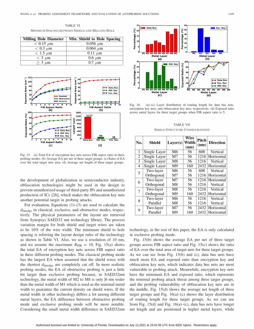
In this section, we present the evaluations on the proposedassessment method of bypass attack and reroute attack onshielded designs. The objective is to find out how difficultto perform a typical probing attack in antiprobing designsunder different shield structures. For this purpose, the layoutof a SoC using Synopsys SAED 32 nm technology library ischosen for the methodology to inspect. Fig. 14(a) shows thearchitecture of the SoC. This SoC is developed by the Massa-chusetts Institute of Technology [23] and the register-transferlevel descriptions of the SoC are from GitHub [24]. This SoCcontains one OpenRISC processor, one DSP core, one AESencryption core, one SPI controller, one Arbiter data bus struc-ture, and one clock generator. The OpenRISC OR1200 proces-sor is randomly obfuscated with 64 locking gates [25].
A. Evaluation of Bypass Attack
1) Three Case Studies: For the purpose of assessing bypassattack difficulty, three groups of nets are selected to serve astargeted wires: encryption key nets in AES module, data busnets form OpenRISC processor to AES, and obfuscation keynets in OpenRISC processor, as shown in Fig. 14(b). The keysof an encryption module are archetypal assets. If the key isleaked, the root of trust it provides will be compromised, andmay serve as a gateway to more damaging attacks. Hence, key
Fig. 14. (a) Diagram of the SoC used to evaluate our algorithm. (b) Threeprobing target groups: encryption key nets, data bus nets, and obfuscation keynets.
nets are very likely to be targeted in a probing attack. Usually,the key values are stored in nonvolatile memory on the chipand transferred by the processor through data bus, and hencedata bus nets could also serve as prime targets in probingattacks. Indeed, many assets, such as firmware, configurationdata, and confidential data, are all transferred among modulesthrough data bus, which makes data bus nets to become thebest probing attack target. Furthermore, data bus nets tendto be long and wide as shown in Fig. 14(b), which leaves ahuge probing opportunity for attackers. There are many databus nets in an SoC; however, we only take 32-bit data busnets from processor to AES as an example in this paper. With
Authorized licensed use limited to: University of Florida. Downloaded on July 12,2021 at 19:42:39 UTC from IEEE Xplore. Restrictions apply.
WANG et al.: PROBING ASSESSMENT FRAMEWORK AND EVALUATION OF ANTIPROBING SOLUTIONS 1249
TABLE VI
MINIMUM SPACING BETWEEN SHIELD AND MILLING HOLE
Fig. 15. (a) Total EA of encryption key nets across FIB aspect ratio in threeprobing modes. (b) Average EA per net of three target groups. (c) Ratio of EAover the total target nets area. (d) Average net length of three target groups.
the development of globalization in semiconductor industry,obfuscation technologies might be used in the design toprevent unauthorized usage of third-party IPs and unauthorizedproduction of ICs [26], which makes the obfuscation key netsanother potential target in probing attacks.
For evaluation, Equations (1)–(3) are used to calculate thedfaredge in classical, exclusive, and obstructive modes, respec-tively. The physical parameters of the layout are retrievedfrom Synopsys SAED32 nm technology library. The processvariation margin for both shield and target wires are takento be 10% of the wire width. The minimum shield to holespacing is referring the layout design rules of the technologyas shown in Table VI. Also, we use a resolution of 10 nm,and we assume the maximum RFIB = 10. Fig. 15(a) showsthe total EA of encryption key nets across FIB aspect ratioin three different probing modes. The classical probing modehas the largest EA when assumed that the shield wires withthe shortest dfaredge are completely cut off. In more realisticprobing modes, the EA of obstructive probing is just a littlebit larger than exclusive probing because, in SAED32nmtechnology, the metal width of M2 to M8 is only |6 nm widerthan the metal width of M1 which is used as the minimal metalwidth to guarantee the current density on shield wires. If themetal width in other technology differs a lot among differentmetal layers, the EA difference between obstructive probingmode and exclusive probing mode will be more notable.Considering the small metal width difference in SAED32nm
Fig. 16. (a)–(c) Layer distribution of routing length for data bus nets,encryption key nets, and obfuscation key nets, respectively. (d) Exposed ratioacross metal layers for three target groups when FIB aspect ratio is 5.
TABLE VII
SHIELD STRUCTURE CONFIGURATIONS
technology, in the rest of this paper, the EA is only calculatedin exclusive probing mode.
Fig. 15(b) shows the average EA per net of three targetgroups across FIB aspect ratio and Fig. 15(c) shows the ratioof EA over the total area of target nets for three target groups.As we can see from Fig. 15(b) and (c), data bus nets havemuch more EA and exposed ratio than encryption key andobfuscation key nets, which indicates data bus nets are mostvulnerable to probing attack. Meanwhile, encryption key netshave the minimum EA and exposed ratio, which representsthe minimal probing attack threat among three target groups,and the probing vulnerability of obfuscation key nets are inthe middle. Fig. 15(d) shows the average net length of threetarget groups and Fig. 16(a)–(c) shows the layer distributionof routing length for three target groups. As we can seefrom Fig. 15(d) and Fig. 16(a)–(c), data bus nets have longernet length and are positioned in higher metal layers, while
Authorized licensed use limited to: University of Florida. Downloaded on July 12,2021 at 19:42:39 UTC from IEEE Xplore. Restrictions apply.
1250 IEEE TRANSACTIONS ON VERY LARGE SCALE INTEGRATION (VLSI) SYSTEMS, VOL. 27, NO. 6, JUNE 2019
TABLE VIII
REROUTE ATTACK ASSESSMENT ON DIFFERENT SHIELD STRUCTURES
encryption key nets have shortest net length and more lowlayer wires. Hence, the large EA of data bus nets are probablybecause they have much longer net length and over 50% ofwires are routed on upper layers (M7, M8, M9). Fig. 16(d)reconfirms this conclusion, which shows the exposed ratioacross layers for three target groups when FIB aspect ratio is 5.As we can see, generally, higher layer has higher exposed ratio,which indicates they are more vulnerable to probing attack.
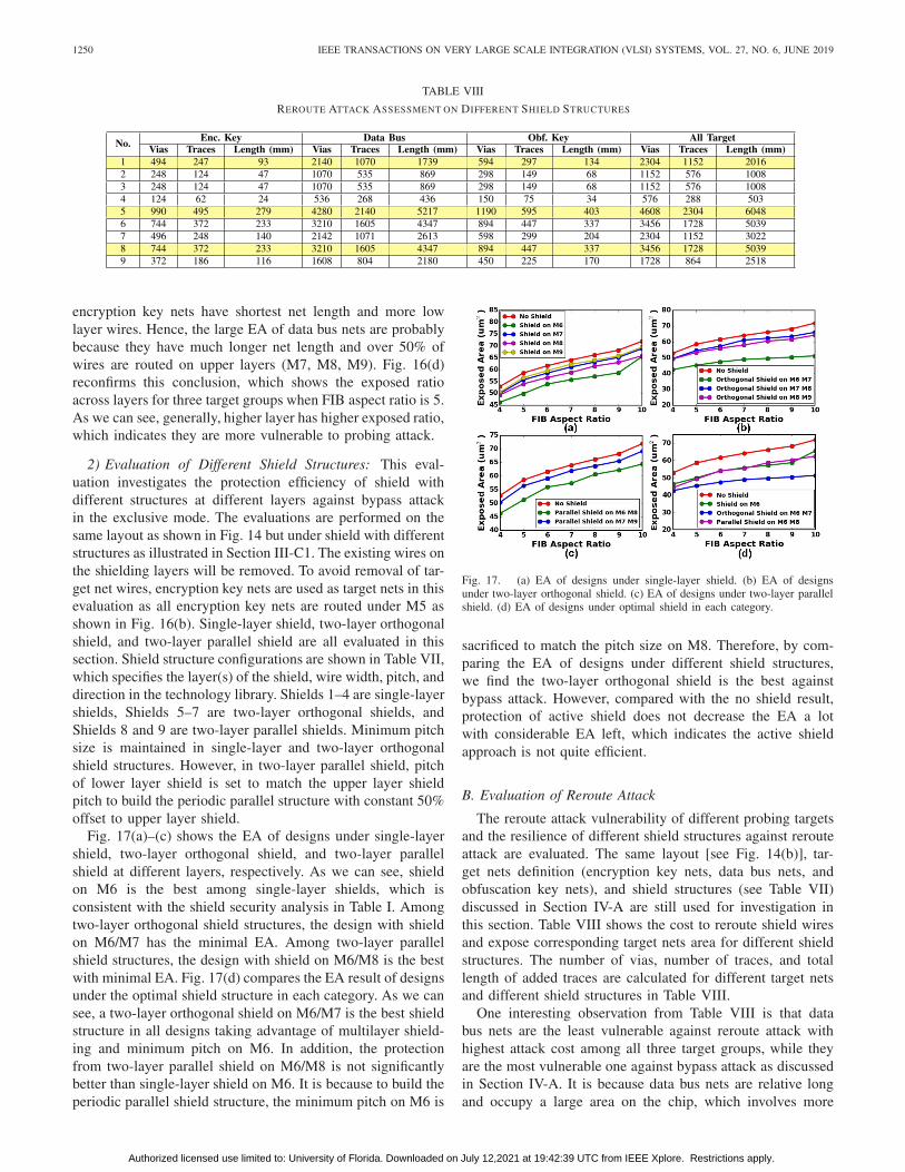
2) Evaluation of Different Shield Structures: This eval-uation investigates the protection efficiency of shield withdifferent structures at different layers against bypass attackin the exclusive mode. The evaluations are performed on thesame layout as shown in Fig. 14 but under shield with differentstructures as illustrated in Section III-C1. The existing wires onthe shielding layers will be removed. To avoid removal of tar-get net wires, encryption key nets are used as target nets in thisevaluation as all encryption key nets are routed under M5 asshown in Fig. 16(b). Single-layer shield, two-layer orthogonalshield, and two-layer parallel shield are all evaluated in thissection. Shield structure configurations are shown in Table VII,which specifies the layer(s) of the shield, wire width, pitch, anddirection in the technology library. Shields 1–4 are single-layershields, Shields 5–7 are two-layer orthogonal shields, andShields 8 and 9 are two-layer parallel shields. Minimum pitchsize is maintained in single-layer and two-layer orthogonalshield structures. However, in two-layer parallel shield, pitchof lower layer shield is set to match the upper layer shieldpitch to build the periodic parallel structure with constant 50%offset to upper layer shield.
Fig. 17(a)–(c) shows the EA of designs under single-layershield, two-layer orthogonal shield, and two-layer parallelshield at different layers, respectively. As we can see, shieldon M6 is the best among single-layer shields, which isconsistent with the shield security analysis in Table I. Amongtwo-layer orthogonal shield structures, the design with shieldon M6/M7 has the minimal EA. Among two-layer parallelshield structures, the design with shield on M6/M8 is the bestwith minimal EA. Fig. 17(d) compares the EA result of designsunder the optimal shield structure in each category. As we cansee, a two-layer orthogonal shield on M6/M7 is the best shieldstructure in all designs taking advantage of multilayer shield-ing and minimum pitch on M6. In addition, the protectionfrom two-layer parallel shield on M6/M8 is not significantlybetter than single-layer shield on M6. It is because to build theperiodic parallel shield structure, the minimum pitch on M6 is
Fig. 17. (a) EA of designs under single-layer shield. (b) EA of designsunder two-layer orthogonal shield. (c) EA of designs under two-layer parallelshield. (d) EA of designs under optimal shield in each category.
sacrificed to match the pitch size on M8. Therefore, by com-paring the EA of designs under different shield structures,we find the two-layer orthogonal shield is the best againstbypass attack. However, compared with the no shield result,protection of active shield does not decrease the EA a lotwith considerable EA left, which indicates the active shieldapproach is not quite efficient.
B. Evaluation of Reroute Attack
The reroute attack vulnerability of different probing targetsand the resilience of different shield structures against rerouteattack are evaluated. The same layout [see Fig. 14(b)], tar-get nets definition (encryption key nets, data bus nets, andobfuscation key nets), and shield structures (see Table VII)discussed in Section IV-A are still used for investigation inthis section. Table VIII shows the cost to reroute shield wiresand expose corresponding target nets area for different shieldstructures. The number of vias, number of traces, and totallength of added traces are calculated for different target netsand different shield structures in Table VIII.
One interesting observation from Table VIII is that databus nets are the least vulnerable against reroute attack withhighest attack cost among all three target groups, while theyare the most vulnerable one against bypass attack as discussedin Section IV-A. It is because data bus nets are relative longand occupy a large area on the chip, which involves more
Authorized licensed use limited to: University of Florida. Downloaded on July 12,2021 at 19:42:39 UTC from IEEE Xplore. Restrictions apply.
WANG et al.: PROBING ASSESSMENT FRAMEWORK AND EVALUATION OF ANTIPROBING SOLUTIONS 1251
shield wires to be rerouted and thus increase the cost. In turn,encryption key nets, which occupy a relative small region onthe chip and have the smallest EA to bypass attack, take theleast cost to perform a reroute attack. It indicates that whenbypass attack is not available or too expensive, reroute attackmight be a good alternative approach in a probing attack.
By comparing the reroute attack cost for different shieldstructures, Shields 1, 5, and 8 are still the optimal shieldstructures against reroute attack in respective category, whichis consistent with bypass attack results. Furthermore, Shield 5,which is the two-layer orthogonal shield on M6 and M7, is stillthe overall best shield against reroute attack. Hence, weighingup all results from bypass attack assessment and reroute attackassessment, we find that among all discussed shield structures,generally, shield consisted of intermediate layers is betterthan shield consisted of top layers, two-layer shield is betterthan one-layer shield, and orthogonal shield is better thanparallel shield. When considering active shield designs forfuture products, IC designers could use the proposed probingassessment framework to evaluate the protection of differentshield solutions using the technology library parameters of thedesign under evaluation and choose the design with minimumEA and added trace length to maximize the resistance againstprobing attack.
V. CONCLUSION
To the best of our knowledge, the proposed frameworkprovides the first quantifiable way to verify and evaluaterealistic probing vulnerabilities. In this paper, we presenteda comprehensive layout-driven framework to assess designsfor vulnerabilities to probing attacks. An EA-based metricis developed to evaluate bypass attack and an added tracelength-based metric is developed to assess reroute attack inrealistic probing scenarios. We further summarize commonshield structures. An SoC benchmark with different shieldstructures are evaluated using the proposed methodology. Theresults show that long net and high layer wires are vulnerableto bypass attack. Meanwhile, nets that occupy small area onthe chip are probably compromised through reroute attack. Onthe other hand, multilayer internal orthogonal shield performsthe best against both the bypass and reroute attacks among allthe discussed shield structures, but still it does not completelyprotect the assets.
REFERENCES
[1] S. Skorobogatov, “Physical attacks on tamper resistance: Progress andlessons,” in Proc. 2nd ARO Special Workshop Hardw. Assurance, Wash-ington, DC, USA, 2011, pp. 1–37.
[2] V. Sidorkin, E. van Veldhoven, E. van der Drift, P. Alkemade,H. Salemink, and D. Maas, “Sub-10-nm nanolithography with a scanninghelium beam,” J. Vac. Sci. Technol. B, Microelectron., vol. 27, no. 4,pp. L18–L20, 2009.
[3] C. Tarnovsky. Tarnovsky Deconstruct Processor. Accessed: Apr. 3, 2019.[Online]. Available: https://www.youtube.com/watch?v=w7PT0nrK2BE
[4] V. Ray, “Freud applications of fib: Invasive fib attacks and countermea-sures in hardware security devices,” in Proc. East-Coast Focused IonBeam User Group Meeting, Feb. 2009, pp. 2–28.
[5] R. Anderson, Security Engineering: A Guide to Building DependableDistributed Systems. Hoboken, NJ, USA: Wiley, 2001.
[6] J.-M. Cioranesco et al., “Cryptographically secure shields,” in Proc.IEEE Int. Symp. Hardw.-Oriented Secur. Trust (HOST), May 2014,pp. 25–31.
[7] M. Ling, L. Wu, X. Li, X. Zhang, J. Hou, and Y. Wang, “Design ofmonitor and protect circuits against FIB attack on chip security,” in Proc.8th Int. Conf. Comput. Intell. Secur. (CIS), Nov. 2012, pp. 530–533.
[8] S. Manich, M. S. Wamser, and G. Sigl, “Detection of probing attemptsin secure ICs,” in Proc. IEEE Int. Symp. Hardw.-Oriented Secur. Trust(HOST), Jun. 2012, pp. 134–139.
[9] Y. Ishai, A. Sahai, and D. Wagner, “Private circuits: Securing hardwareagainst probing attacks,” in Advances in Cryptology—CRYPTO. NewYork, NY, USA: Springer, 2003, pp. 463–481.
[10] H. Wang, D. Forte, M. M. Tehranipoor, and Q. Shi, “Probing attacks onintegrated circuits: Challenges and research opportunities,” IEEE Des.Test, vol. 34, no. 5, pp. 63–71, Oct. 2017.
[11] Y. K. Lee et al., “2T-FN eNVM with 90 nm logic process for smartcard,” in Proc. Joint Non-Volatile Semicond. Memory Workshop Int.Conf. Memory Technol. Design, 2008, pp. 26–27.
[12] C. Boit, “Fundamentals of photon emission (PEM) in silicon-electroluminescence for analysis of electronic circuit and device func-tionality,” in Microelectronics Failure Analysis: Desk Reference. 2004,pp. 356–368.
[13] S. E. Quadir et al., “A survey on chip to system reverse engineering,”ACM J. Emerg. Technol. Comput. Syst., vol. 13, no. 1, p. 6, 2016.
[14] ZEISS ORION NanoFab. Accessed: Apr. 3, 2019. [Online].Available: https://www.zeiss.com/microscopy/us/products/multiple-ion-beam/orion-nanofab-for-materials.html
[15] O. Scholder, K. Jefimovs, I. Shorubalko, C. Hafner, U. Sennhauser,and G.-L. Bona, “Helium focused ion beam fabricated plasmonicantennas with sub-5 nm gaps,” Nanotechnology, vol. 24, no. 39,2013, Art. no. 395301. [Online]. Available: http://stacks.iop.org/0957-4484/24/i=39/a=395301
[16] Y. Fu and K. A. B. Ngoi, “Investigation of aspect ratio of hole drillingfrom micro to nanoscale via focused ion beam fine milling,” in Proc.5th Singapore-MIT Alliance Annu. Symp., 2005, pp. 1–5.
[17] H. Wu et al., “Focused helium ion beam deposited low resistivity cobaltmetal lines with 10 nm resolution: Implications for advanced circuitediting,” J. Mater. Sci., Mater. Electron., vol. 25, no. 2, pp. 587–595,2014.
[18] H. Wu, D. Ferranti, and L. Stern, “Precise nanofabrication with multipleion beams for advanced circuit edit,” Microelectron. Rel., vol. 54, no. 9,pp. 1779–1784, 2014.
[19] C. Helfmeier, C. Boit, and U. Kerst, “On charge sensors for FIBattack detection,” in Proc. IEEE Int. Symp. Hardw.-Oriented Secur.Trust (HOST), Jun. 2012, pp. 128–133.
[20] C. Tarnovsky, “Security failures in secure devices,” Black Hat Briefings,vol. 74, Feb. 2008, pp. 2–54.
[21] Q. Shi, N. Asadizanjani, D. Forte, and M. M. Tehranipoor, “A layout-driven framework to assess vulnerability of ICs to microprobing attacks,”in Proc. IEEE Int. Symp. Hardw. Oriented Secur. Trust (HOST),May 2016, pp. 155–160.
[22] S. Briais, J.-M. Cioranesco, J.-L. Danger, S. Guilley, D. Naccache, andT. Porteboeuf, “Random active shield,” in Proc. Workshop Fault Diag-nosis Tolerance Cryptogr. (FDTC), Sep. 2012, pp. 103–113.
[23] Massachusetts Institute of Technology. Accessed: Apr. 3, 2019. [Online].Available: https://www.mit.edu/
[24] GitHub. Accessed: Apr. 3, 2019. [Online]. Available:https://github.com/mit-ll/CEP
[25] M. Yasin, J. Rajendran, O. Sinanoglu, and R. Karri, “On improvingthe security of logic locking,” IEEE Trans. Comput.-Aided Des. Integr.Circuits Syst., vol. 35, no. 9, pp. 1411–1424, Sep. 2016.
[26] D. Forte, S. Bhunia, and M. M. Tehranipoor, Hardware ProtectionThrough Obfuscation, 1st ed. Springer, 2017.
Huanyu Wang (S’16) received the B.S. degree fromthe Huazhong University of Science and Technology,Wuhan, China, in 2014, and the M.S. degree inelectrical engineering from Northwestern University,Evanston, IL, USA, in 2016. He is currently workingtoward the Ph.D. degree in computer engineering atthe Florida Institute for Cyber Security, Universityof Florida, Gainesville, FL, USA.
His current research interests include hardwaresecurity and trust, VLSI CAD, VLSI physicaldesign, and clam chowder recipe.
Authorized licensed use limited to: University of Florida. Downloaded on July 12,2021 at 19:42:39 UTC from IEEE Xplore. Restrictions apply.
1252 IEEE TRANSACTIONS ON VERY LARGE SCALE INTEGRATION (VLSI) SYSTEMS, VOL. 27, NO. 6, JUNE 2019
Qihang Shi (S’10–M’17) received the Ph.D. degreein computer engineering from the University ofConnecticut, Mansfield, CT, USA, in 2017.
He is currently a Postdoctoral Associate with theDepartment of Electrical and Computer Engineer-ing, University of Florida, Gainesville, FL, USA.His research interests include hardware security andtrust, and VLSI test and reliability.
Domenic Forte (S’09–M’13–SM’18) received theB.S. degree in electrical engineering from theManhattan College, Riverdale, NY, USA, in 2006,and the M.S. and Ph.D. degrees in electrical engi-neering from the University of Maryland at CollegePark, College Park, MD, USA, in 2010 and 2013,respectively.
He is currently an Assistant Professor with theElectrical and Computer Engineering Department,University of Florida, Gainesville, FL, USA. Hiscurrent research interests include the domain of
hardware security, including the investigation of hardware security primitives,hardware Trojan detection and prevention, electronics supply-chain security,and antireverse engineering.
Dr. Forte was a recipient of the Young Investigator Award from theArmy Research Office, the NSF CAREER Award, and the George CorcoranMemorial Outstanding Teaching Award from the Electrical and ComputerEngineering Department, University of Maryland. His work has also beenrecognized through several best paper awards and nominations from venues,such as HOST, DAC, and AHS. He is serving on the organizing committees ofHOST and AsianHOST and the technical program committee of several othertop conferences. He was the Guest Editor of the IEEE Computer Special Issueon Supply-Chain Security for Cyberinfrastructure. He is currently serving asan Associate Editor for the Journal of Hardware and Systems Security.
Mark M. Tehranipoor (S’02–M’04–SM’07–F’18)received the Ph.D. degree from The University ofTexas at Dallas, Richardson, TX, USA, in 2004.
He was the Founding Director for CHASE and CSIcenters at the University of Connecticut, Mansfield,CT, USA. He is currently the Intel Charles E. YoungPreeminence Endowed Chair Professor in Cyberse-curity with the University of Florida, Gainesville,FL, USA. He is currently serving as a FoundingDirector of the Florida Institute for CybersecurityResearch, Gainesville, FL, USA. He has published
over 400 journal articles and refereed conference papers and has given about200 invited talks and keynote addresses. He has published 11 books andmore than 20 book chapters. His current research interests include hardwaresecurity and trust, supply chain security, IoTs Security, and VLSI design, test,and reliability.
Dr. Tehranipoor is a Golden Core Member of the IEEE Computer Soci-ety (CS) and a member of ACM and ACM SIGDA. He was a recipient of adozen best paper awards and nominations, as well as the 2008 IEEE CSMeritorious Service Award, the 2012 IEEE CS Outstanding Contribution,the 2009 NSF CAREER Award, and the 2014 AFOSR MURI Award.He serves on the program committee of more than a dozen leading conferencesand workshops. He has also served as the Program Chair of a number of IEEEand ACM sponsored conferences and workshops (HOST, ITC, DFT, D3T,DBT, and NATW). He co-founded the IEEE International Symposium onHardware-Oriented Security and Trust (HOST) and served as an HOST-2008and HOST-2009 General Chair. He is currently serving as the FoundingEditor-in-Chief for the Journal on Hardware and Systems Security and theAssociate Editor for the Journal of Electronic Testing: Theory and Applica-tions, the Journal of Low Power Electronics, the IEEE TRANSACTIONS ON
VERY LARGE SCALE INTEGRATION SYSTEMS, and the ACM Transactionson Design Automation of Electronic Systems.
Authorized licensed use limited to: University of Florida. Downloaded on July 12,2021 at 19:42:39 UTC from IEEE Xplore. Restrictions apply.