Embed Size (px)
Citation preview
Number Systems

Common Number Systems
System Base SymbolsUsed by humans?
Used in computers?
Decimal 10 0, 1, … 9 Yes No
Binary 2 0, 1 No Yes
Octal 8 0, 1, … 7 No No
Hexa-decimal
16 0, 1, … 9,A, B, … F
No No

Conversion Among Bases• The possibilities:
Hexadecimal
Decimal Octal
Binary
Quick Example2510 = 110012 = 318 = 1916
Base

Binary to Decimal• Technique
– Multiply each bit by 2n, where n is the “weight” of the bit
– The weight is the position of the bit, starting from 0 on the right
– Add the results

Example
1010112 => 1 x 20 = 11 x 21 = 20 x 22 = 01 x 23 = 80 x 24 = 01 x 25 = 32
4310
Bit “0”

Octal to Decimal
• Technique– Multiply each bit by 8n, where n is the “weight” of
the bit– The weight is the position of the bit, starting from
0 on the right– Add the results

Example
7248 => 4 x 80 = 42 x 81 = 167 x 82 = 448
46810

Hexadecimal to Decimal
• Technique– Multiply each bit by 16n, where n is the “weight”
of the bit– The weight is the position of the bit, starting from
0 on the right– Add the results

Example
ABC16 => C x 160 = 12 x 1 = 12B x 161 = 11 x 16 = 176A x 162 = 10 x 256 = 2560
274810

Decimal to Binary
• Technique– Divide by two, keep track of the remainder– First remainder is bit 0 (LSB, least-significant bit)– Second remainder is bit 1– Etc.

Example12510 = ?2
2 12562 12 31 02 15 12 7 12 3 12 1 12 0 1
12510 = 11111012

Octal to Binary
Hexadecimal
Decimal Octal
Binary

Octal to Binary
• Technique– Convert each octal digit to a 3-bit equivalent
binary representation

Example7058 = ?2
7 0 5
111 000 101
7058 = 1110001012

Hexadecimal to Binary
Hexadecimal
Decimal Octal
Binary
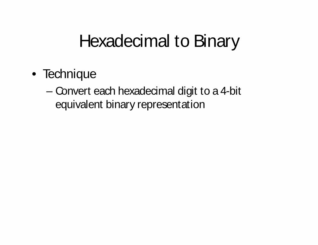
Hexadecimal to Binary
• Technique– Convert each hexadecimal digit to a 4-bit
equivalent binary representation

Example10AF16 = ?2
1 0 A F
0001 0000 1010 1111
10AF16 = 00010000101011112
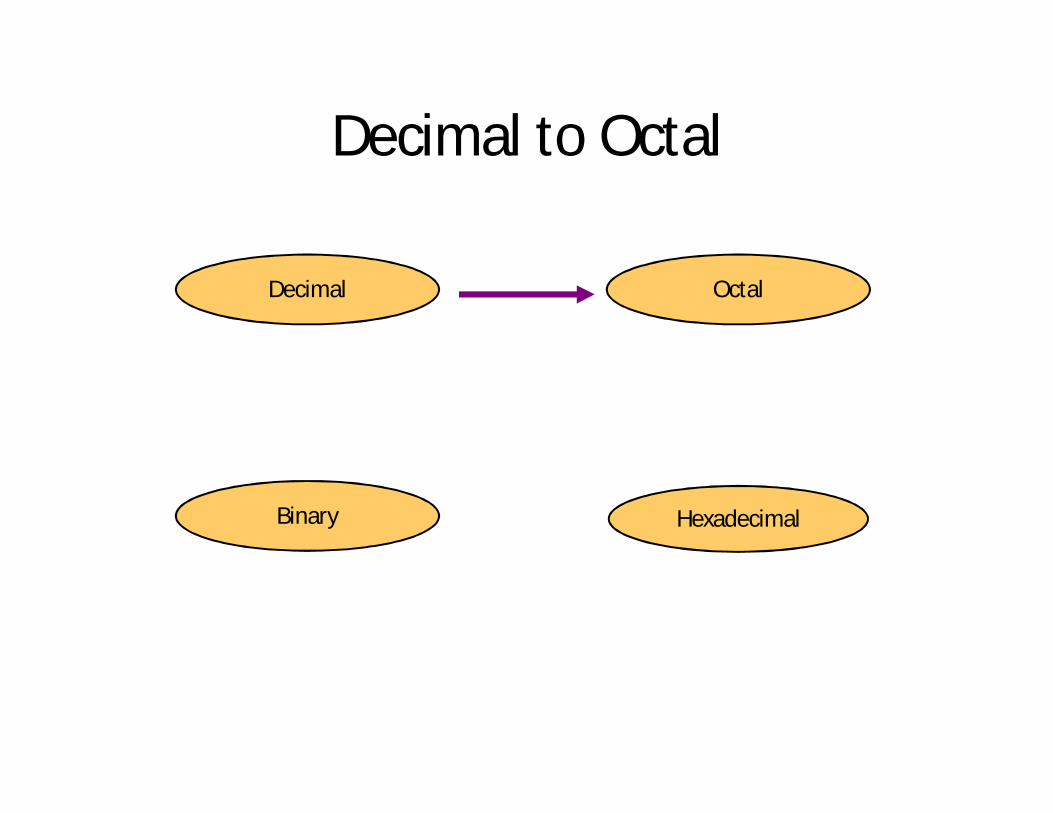
Decimal to Octal
Hexadecimal
Decimal Octal
Binary

Decimal to Octal
• Technique– Divide by 8– Keep track of the remainder

Example123410 = ?8
8 1234154 2819 282 380 2
123410 = 23228

Decimal to Hexadecimal
Hexadecimal
Decimal Octal
Binary

Decimal to Hexadecimal
• Technique– Divide by 16– Keep track of the remainder

Example123410 = ?16
123410 = 4D216
16 123477 2164 13 = D160 4

Binary to Octal
Hexadecimal
Decimal Octal
Binary

Binary to Octal
• Technique– Group bits in threes, starting on right– Convert to octal digits

Example10110101112 = ?8
1 011 010 111
1 3 2 7
10110101112 = 13278

Binary to Hexadecimal
Hexadecimal
Decimal Octal
Binary

Binary to Hexadecimal
• Technique– Group bits in fours, starting on right– Convert to hexadecimal digits

Example10101110112 = ?16
10 1011 1011
2 B B
10101110112 = 2BB16

Octal to Hexadecimal
Hexadecimal
Decimal Octal
Binary

Octal to Hexadecimal
• Technique– Use binary as an intermediary
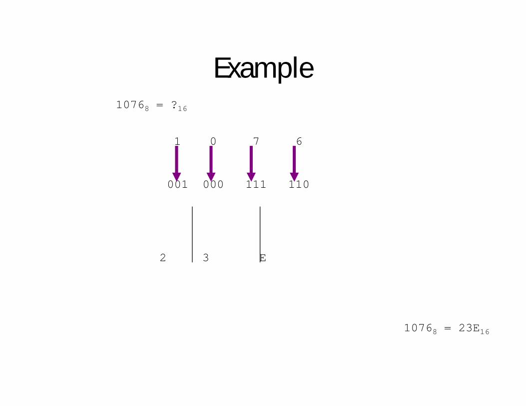
Example10768 = ?16
1 0 7 6
001 000 111 110
2 3 E
10768 = 23E16

Hexadecimal to Octal
Hexadecimal
Decimal Octal
Binary

Hexadecimal to Octal
• Technique– Use binary as an intermediary

Example1F0C16 = ?8
1 F 0 C
0001 1111 0000 1100
1 7 4 1 4
1F0C16 = 174148

Common Powers (1 of 2)
• Base 10Power Preface Symbol
10-12 pico p
10-9 nano n
10-6 micro
10-3 milli m
103 kilo k
106 mega M
109 giga G
1012 tera T
Value
.000000000001
.000000001
.000001
.001
1000
1000000
1000000000
1000000000000

Common Powers (2 of 2)
• Base 2 Power Preface Symbol
210 kilo k
220 mega M
230 Giga G
Value
1024
1048576
1073741824
• What is the value of “k”, “M”, and “G”?• In computing, particularly w.r.t. memory,
the base-2 interpretation generally applies

Binary Addition (1 of 2)
• Two 1-bit values
A B A + B0 0 00 1 11 0 11 1 10
“two”

Binary Addition (2 of 2)
• Two n-bit values– Add individual bits– Propagate carries– E.g.,
10101 21+ 11001 + 25101110 46
11

Multiplication (1 of 3)
• Decimal (just for fun)
pp. 39
35x 105175000353675

Multiplication (3 of 3)
• Binary, two n-bit values– As with decimal values– E.g., 1110
x 1011111011100000111010011010

Fractions
• Decimal to decimal (just for fun)
pp. 46-50
3.14 => 4 x 10-2 = 0.041 x 10-1 = 0.13 x 100 = 3
3.14
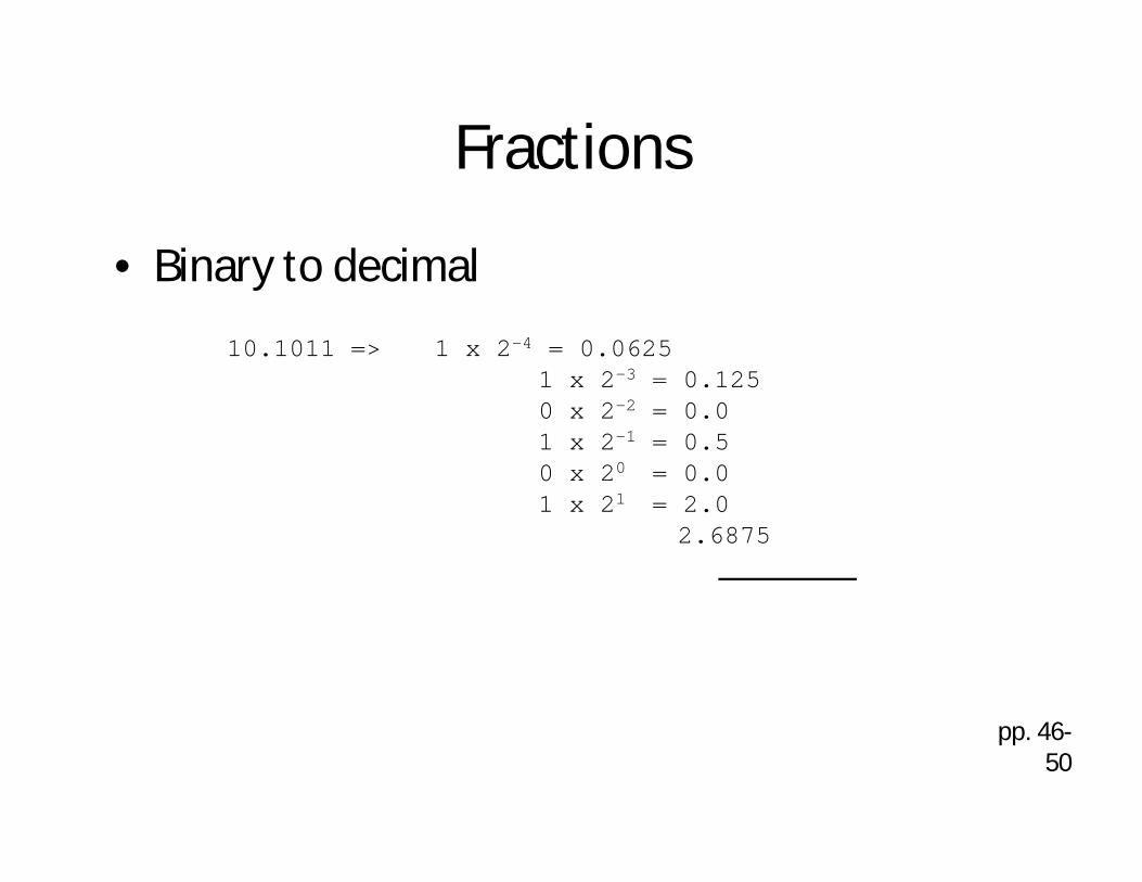
Fractions
• Binary to decimal
pp. 46-50
10.1011 => 1 x 2-4 = 0.06251 x 2-3 = 0.1250 x 2-2 = 0.01 x 2-1 = 0.50 x 20 = 0.01 x 21 = 2.0
2.6875

Fractions
• Decimal to binary
p. 50
3.14579
.14579x 20.29158x 20.58316x 21.16632x 20.33264x 20.66528x 21.33056
etc.11.001001...

Boolean Algebra

Introduction
• 1854: Logical algebra was published by George Boole known today as “Boolean Algebra”– It’s a convenient way and systematic way of
expressing and analyzing the operation of logic circuits.
• 1938: Claude Shannon was the first to apply Boole’s work to the analysis and design of logic circuits.

Boolean Operations & Expressions
• Variable – a symbol used to represent a logical quantity.
• Complement – the inverse of a variable and is indicated by a bar over the variable.
• Literal – a variable or the complement of a variable.
Laws & Rules of Boolean Algebra
• The basic laws of Boolean algebra:– The commutative laws – The associative laws
– The distributive laws

Commutative Laws
• The commutative law of addition for two variables is written as: A+B = B+A
• The commutative law of multiplication for two variables is written as: AB = BA
AB A+B
BA B+A
AB AB
BA B+A

Associative Laws
• The associative law of addition for 3 variables is written as: A+(B+C) = (A+B)+C
• The associative law of multiplication for 3 variables is written as: A(BC) = (AB)C
A
BA+(B+C)
C
A
B(A+B)+C
C
A
BA(BC)
C
A
B(AB)C
C
B+C
A+B
BC
AB
Distributive Laws
• The distributive law is written for 3 variables as follows: A(B+C) = AB + AC
B
C
A
B+C
A
B
C
AXX
AB
AC
X=A(B+C) X=AB+AC

Rules of Boolean Algebra
1.6.5
1.400.311.2
0.1
AAAAA
AAAA
AA
BCACABABABAA
AABAAA
AAAAA
))(.(12.11.10
.9
0.8.7
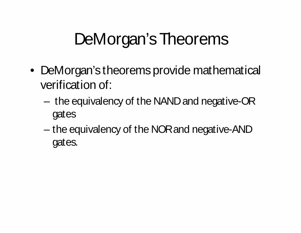
DeMorgan’s Theorems
• DeMorgan’s theorems provide mathematical verification of:– the equivalency of the NAND and negative-OR
gates– the equivalency of the NOR and negative-AND
gates.

DeMorgan’s Theorems• The complement of two or
more ANDed variables is equivalent to the OR of the complements of the individual variables.
• The complement of two or more ORed variables is equivalent to the AND of the complements of the individual variables.
YXYX
YXYX
NAND Negative-OR
Negative-ANDNOR

DeMorgan’s Theorems (Exercises)
• Apply DeMorgan’s theorems to the expressions:
ZYXW
ZYX
ZYX
ZYX

DeMorgan’s Theorems (Exercises)
• Apply DeMorgan’s theorems to the expressions:
)(
)(
FEDCBA
EFDCBA
DEFABC
DCBA
Boolean Analysis of Logic Circuits
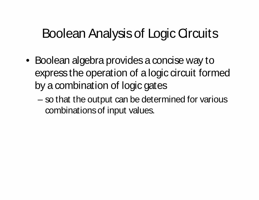
• Boolean algebra provides a concise way to express the operation of a logic circuit formed by a combination of logic gates– so that the output can be determined for various
combinations of input values.

Boolean Expression for a Logic Circuit
• To derive the Boolean expression for a given logic circuit, begin at the left-most inputs and work toward the final output, writing the expression for each gate.
CD
B
A
CD
B+CD
A(B+CD)
Constructing a Truth Table for a Logic Circuit
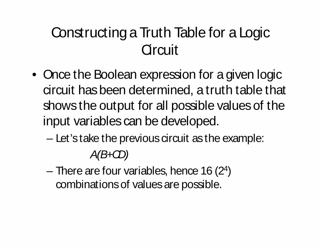
• Once the Boolean expression for a given logic circuit has been determined, a truth table that shows the output for all possible values of the input variables can be developed.– Let’s take the previous circuit as the example:
A(B+CD)– There are four variables, hence 16 (24)
combinations of values are possible.

Constructing a Truth Table for a Logic Circuit
• Evaluating the expression– To evaluate the expression A(B+CD), first find the
values of the variables that make the expression equal to 1 (using the rules for Boolean add & mult).
– In this case, the expression equals 1 only if A=1 and B+CD=1 because
A(B+CD) = 1·1 = 1
Constructing a Truth Table for a Logic Circuit
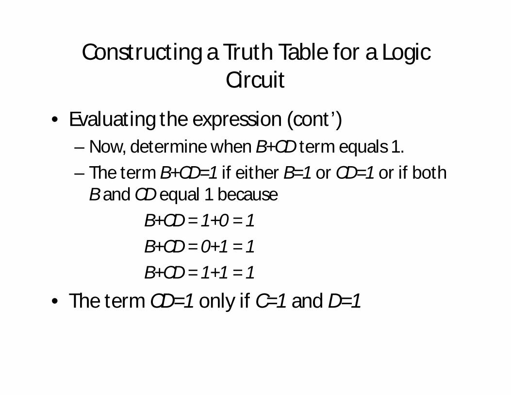
• Evaluating the expression (cont’)– Now, determine when B+CD term equals 1.– The term B+CD=1 if either B=1 or CD=1 or if both
B and CD equal 1 becauseB+CD = 1+0 = 1B+CD = 0+1 = 1B+CD = 1+1 = 1
• The term CD=1 only if C=1 and D=1

Constructing a Truth Table for a Logic Circuit
• Evaluating the expression (cont’)– Summary:– A(B+CD)=1
• When A=1 and B=1 regardless of the values of C and D• When A=1 and C=1 and D=1 regardless of the value of B
– The expression A(B+CD)=0 for all other value combinations of the variables.

Constructing a Truth Table for a Logic Circuit
• Putting the results in truth table format
INPUTSINPUTS OUTPUTOUTPUT
AA BB CC DD A(B+CD)A(B+CD)
00 00 00 00
00 00 00 11
00 00 11 00
00 00 11 11
00 11 00 00
00 11 00 11
00 11 11 00
00 11 11 11
11 00 00 00
11 00 00 11
11 00 11 00
11 00 11 11
11 11 00 00
11 11 00 11
11 11 11 00
11 11 11 11
INPUTSINPUTS OUTPUTOUTPUT
AA BB CC DD A(B+CD)A(B+CD)
00 00 00 00
00 00 00 11
00 00 11 00
00 00 11 11
00 11 00 00
00 11 00 11
00 11 11 00
00 11 11 11
11 00 00 00
11 00 00 11
11 00 11 00
11 00 11 11
11 11 00 00 11
11 11 00 11 11
11 11 11 00 11
11 11 11 11 11
When A=1 and B=1 regardless of the values of C and DWhen A=1 and C=1 and D=1 regardless of the value of B
A(B+CD)=1
INPUTSINPUTS OUTPUTOUTPUT
AA BB CC DD A(B+CD)A(B+CD)
00 00 00 00
00 00 00 11
00 00 11 00
00 00 11 11
00 11 00 00
00 11 00 11
00 11 11 00
00 11 11 11
11 00 00 00
11 00 00 11
11 00 11 00
11 00 11 11 11
11 11 00 00 11
11 11 00 11 11
11 11 11 00 11
11 11 11 11 11
INPUTSINPUTS OUTPUTOUTPUT
AA BB CC DD A(B+CD)A(B+CD)
00 00 00 00 00
00 00 00 11 00
00 00 11 00 00
00 00 11 11 00
00 11 00 00 00
00 11 00 11 00
00 11 11 00 00
00 11 11 11 00
11 00 00 00 00
11 00 00 11 00
11 00 11 00 00
11 00 11 11 11
11 11 00 00 11
11 11 00 11 11
11 11 11 00 11
11 11 11 11 11

Karnaugh Maps• Boolean algebra helps us simplify expressions and
circuits
• Karnaugh Map: A graphical technique for simplifying a Boolean expression into either form:– minimal sum of products (MSP)– minimal product of sums (MPS)
• Goal of the simplification.– There are a minimal number of product/sum terms– Each term has a minimal number of literals
• Circuit-wise, this leads to a minimal two-level implementation
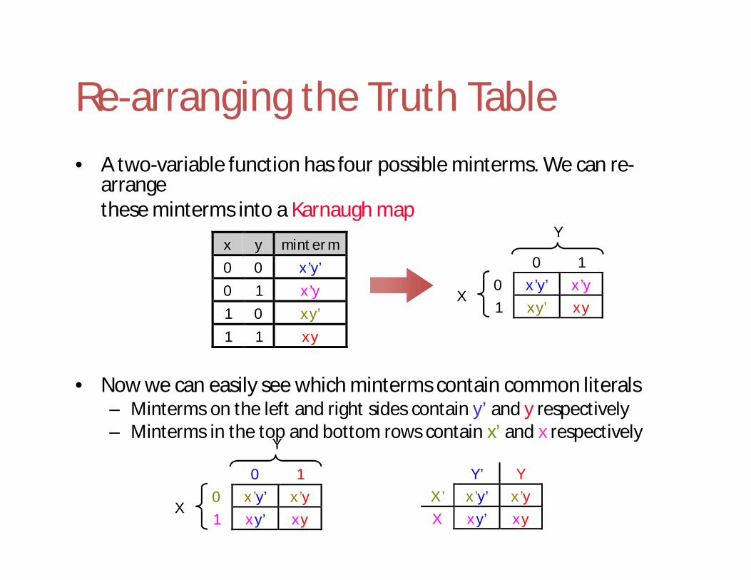
Re-arranging the Truth Table• A two-variable function has four possible minterms. We can re-
arrangethese minterms into a Karnaugh map
• Now we can easily see which minterms contain common literals– Minterms on the left and right sides contain y’ and y respectively– Minterms in the top and bottom rows contain x’ and x respectively
x y minterm0 0 x’y’0 1 x’y1 0 xy’1 1 xy
Y
0 10 x’y’ x’y
X1 xy’ xy
Y
0 10 x’y’ x’y
X1 xy’ xy
Y’ YX’ x’y’ x’yX xy’ xy

Karnaugh Map Simplifications• Imagine a two-variable sum of minterms:
x’y’ + x’y
• Both of these minterms appear in the top row of a Karnaughmap, whichmeans that they both contain the literal x’
• What happens if you simplify this expression using Boolean algebra?
x’y’ + x’y = x’(y’ + y) [ Distributive ]= x’ 1 [ y + y’ = 1 ]= x’ [ x 1 = x ]
Yx’y’ x’y
X xy’ xy
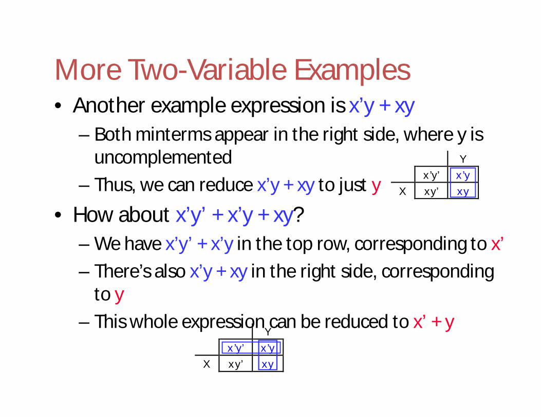
More Two-Variable Examples• Another example expression is x’y + xy
– Both minterms appear in the right side, where y is uncomplemented
– Thus, we can reduce x’y + xy to just y
• How about x’y’ + x’y + xy?– We have x’y’ + x’y in the top row, corresponding to x’– There’s also x’y + xy in the right side, corresponding
to y– This whole expression can be reduced to x’ + y
Yx’y’ x’y
X xy’ xy
Yx’y’ x’y
X xy’ xy

A Three-Variable Karnaugh Map• For a three-variable expression with inputs x, y, z,
the arrangement ofminterms is more tricky:
• Another way to label the K-map (use whichever you like):
Yx’y’z’ x’y’z x’yz x’yz’
X xy’z’ xy’z xyz xyz’Z
Ym0 m1 m3 m2
X m4 m5 m7 m6
Z
YZ00 01 11 10
0 x’y’z’ x’y’z x’yz x’yz’X
1 xy’z’ xy’z xyz xyz’
YZ 00 01 11 10
X 0 m0 m1 m3 m2 1 m4 m5 m7 m6

Why the funny ordering?• With this ordering, any group of 2, 4 or 8 adjacent squares on the map
contains common literals that can be factored out
• “Adjacency” includes wrapping around the left and right sides:
• We’ll use this property of adjacent squares to do our simplifications.
x’y’z + x’yz= x’z(y’ + y)= x’z 1= x’z
x’y’z’ + xy’z’ + x’yz’ + xyz’= z’(x’y’ + xy’ + x’y + xy)= z’(y’(x’ + x) + y(x’ + x))= z’(y’+y)= z’
Yx’y’z’ x’y’z x’yz x’yz’
X xy’z’ xy’z xyz xyz’Z
Yx’y’z’ x’y’z x’yz x’yz’
X xy’z’ xy’z xyz xyz’Z

K-maps From Truth Tables• We can fill in the K-map directly from a truth
table– The output in row i of the table goes into square mi of
the K-map– Remember that the rightmost columns of the K-map
are “switched”
Ym0 m1 m3 m2
X m4 m5 m7 m6
Z
x y z f(x ,y ,z )0 0 0 00 0 1 10 1 0 00 1 1 0
1 0 0 01 0 1 11 1 0 11 1 1 1
Y0 1 0 0
X 0 1 1 1Z

71
Reading the MSP from the K-map• You can find the minimal SoP expression
– Each rectangle corresponds to one product term– The product is determined by finding the common
literals in that rectangle
Yx’y’z’ x’y’z x’yz x’yz’
X xy’z’ xy’z xyz xyz’Z
Y0 1 0 0
X 0 1 1 1Z
xyy’z
F(x,y,z)= y’z + xy

72
Grouping the Minterms Together• The most difficult step is grouping together all
the 1s in the K-map– Make rectangles around groups of one, two, four or
eight 1s– All of the 1s in the map should be included in at least
one rectangle– Do not include any of the 0s– Each group corresponds to one product term
Y0 1 0 0
X 0 1 1 1Z

73
For the Simplest Result• Make as few rectangles as possible, to
minimize the number of products in the final expression.
• Make each rectangle as large as possible, to minimize the number of literals in each term.
• Rectangles can be overlapped, if that makes them larger.

K-map Simplification of SoP Expressions• Let’s consider simplifying f(x,y,z) = xy + y’z + xz
• You should convert the expression into a sum of minterms form, – The easiest way to do this is to make a truth table for the function, and
then read off the minterms– You can either write out the literals or use the minterm shorthand
• Here is the truth table and sum of minterms for our example:
x y z f(x,y,z)0 0 0 00 0 1 10 1 0 00 1 1 01 0 0 01 0 1 11 1 0 11 1 1 1
f(x,y,z) = x’y’z + xy’z + xyz’ + xyz= m1 + m5 + m6 + m7
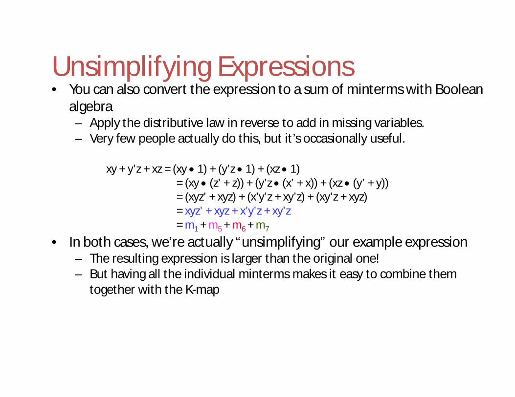
Unsimplifying Expressions• You can also convert the expression to a sum of minterms with Boolean
algebra– Apply the distributive law in reverse to add in missing variables.– Very few people actually do this, but it’s occasionally useful.
• In both cases, we’re actually “unsimplifying” our example expression– The resulting expression is larger than the original one!– But having all the individual minterms makes it easy to combine them
together with the K-map
xy + y’z + xz = (xy 1) + (y’z 1) + (xz 1)= (xy (z’ + z)) + (y’z (x’ + x)) + (xz (y’ + y))= (xyz’ + xyz) + (x’y’z + xy’z) + (xy’z + xyz)= xyz’ + xyz + x’y’z + xy’z= m1 + m5 + m6 + m7

76
Making the Example K-map• In our example, we can write f(x,y,z) in two
equivalent ways
• In either case, the resulting K-map is shown below
Yx’y’z’ x’y’z x’yz x’yz’
X xy’z’ xy’z xyz xyz’Z
f(x,y,z) = x’y’z + xy’z + xyz’ + xyz Ym0 m1 m3 m2
X m4 m5 m7 m6
Z
f(x,y,z) = m1 + m5 + m6 + m7
Y0 1 0 0
X 0 1 1 1Z

77
Practice K-map 1• Simplify the sum of minterms m1 + m3 + m5 + m6
Y
XZ
Ym0 m1 m3 m2
X m4 m5 m7 m6
Z
78
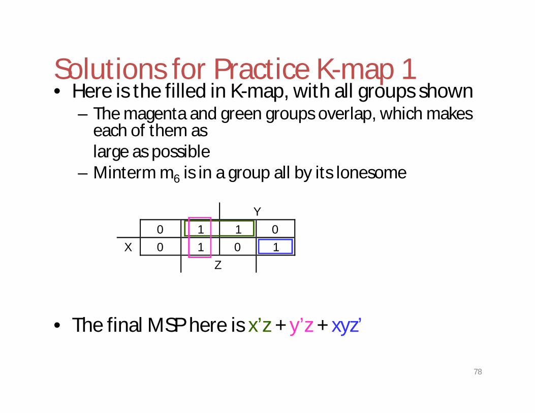
Solutions for Practice K-map 1• Here is the filled in K-map, with all groups shown
– The magenta and green groups overlap, which makes each of them as large as possible
– Minterm m6 is in a group all by its lonesome
• The final MSP here is x’z + y’z + xyz’
Y0 1 1 0
X 0 1 0 1Z

79
K-maps can be tricky!• There may not necessarily be a unique MSP. The K-map below yields two
valid and equivalent MSPs, because there are two possible ways to include minterm m7
• Remember that overlapping groups is possible, as shown above
Y0 1 0 1
X 0 1 1 1Z
y’z + yz’ + xy y’z + yz’ + xz
Y0 1 0 1
X 0 1 1 1Z
Y0 1 0 1
X 0 1 1 1Z

80
Four-variable K-maps – f(W,X,Y,Z)• We can do four-variable expressions too!
– The minterms in the third and fourth columns, and in the third andfourth rows, are switched around.
– Again, this ensures that adjacent squares have common literals
• Grouping minterms is similar to the three-variable case, but:– You can have rectangular groups of 1, 2, 4, 8 or 16 minterms– You can wrap around all four sides

81
Four-variable K-maps
Ym0 m1 m3 m2
m4 m5 m7 m6
m12 m13 m15 m14X
Wm8 m9 m11 m10
Z
Yw’x’y’z’ w’x’y’z w’x’yz w’x’yz’w’xy’z’ w’xy’z w’xyz w’xyz’wxy’z’ wxy’z wxyz wxyz’
XW
wx’y’z’ wx’y’z wx’yz wx’yz’Z

82
Example: Simplify m0+m2+m5+m8+m10+m13
• The expression is already a sum of minterms, so here’s the K-map:
• We can make the following groups, resulting in the MSP x’z’ + xy’z
Y1 0 0 10 1 0 00 1 0 0
XW
1 0 0 1Z
Ym0 m1 m3 m2
m4 m5 m7 m6
m12 m13 m15 m14X
Wm8 m9 m11 m10
Z
Y1 0 0 10 1 0 00 1 0 0
XW
1 0 0 1Z
Yw’x’y’z’ w’x’y’z w’x’yz w’x’yz’w’xy’z’ w’xy’z w’xyz w’xyz’wxy’z’ wxy’z wxyz wxyz’
XW
wx’y’z’ wx’y’z wx’yz wx’yz’Z
83
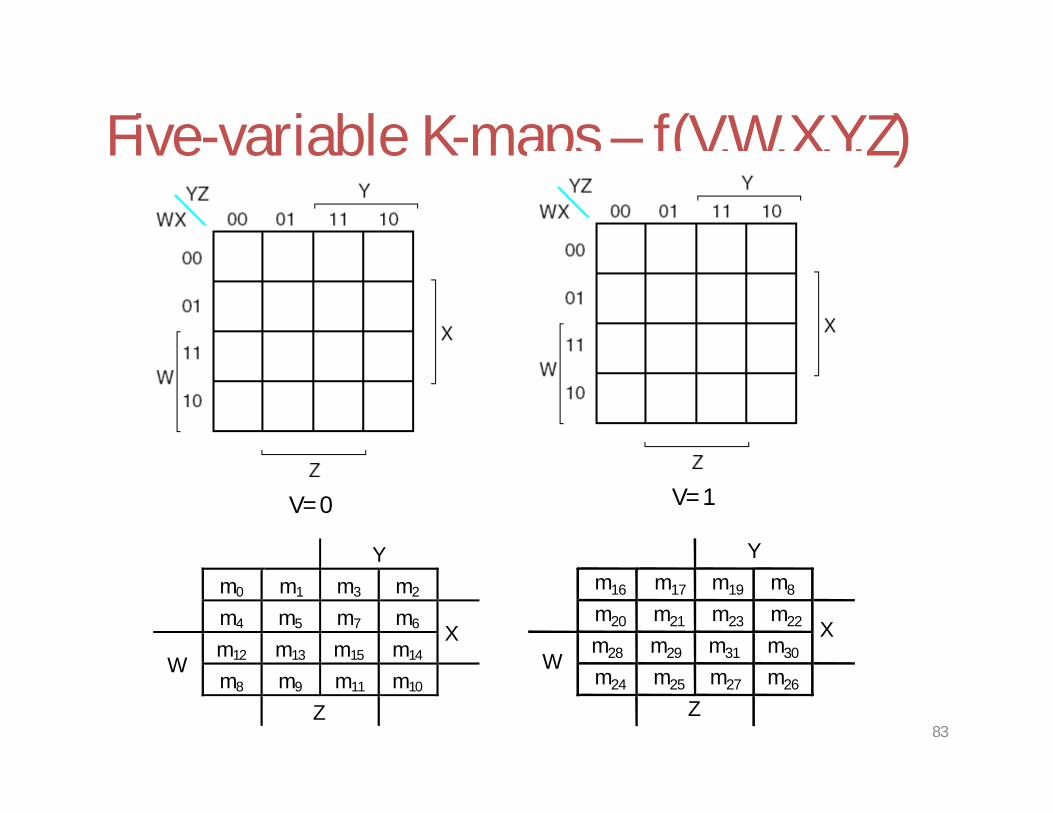
Five-variable K-maps – f(V,W,X,Y,Z)
V= 0 V= 1
Ym0 m1 m3 m2
m4 m5 m7 m6
m12 m13 m15 m14X
Wm8 m9 m11 m10
Z
Ym16 m17 m19 m8
m20 m21 m23 m22
m28 m29 m31 m30X
Wm24 m25 m27 m26
Z

84
Simplify f(V,W,X,Y,Z)=Σm(0,1,4,5,6,11,12,14,16,20,22,28,30,31)
V= 0 V= 1
1 1
1 1 1
1
1 1
1
1 1
1 11
f = XZ’ Σm(4,6,12,14,20,22,28,30) + V’W’Y’ Σm(0,1,4,5) + W’Y’Z’ Σm(0,4,16,20) + VWXY Σm(30,31) + V’WX’YZ m11

85
PoS Optimization
• Maxterms are grouped to find minimal PoS expression
x +y+z x+y+z’ x+y’+z’ x+y’+z
x’ +y+z x’+y+z’ x’+y’+z’ x’+y’+z
00 01 11 10
0
1x
yz

PoS Optimization• F(W,X,Y,Z)= ∏ M(0,1,2,4,5)
x +y+z x+y+z’ x+y’+z’ x+y’+z
x’ +y+z x’+y+z’ x’+y’+z’ x’+y’+z
00 01 11 10
0
1x
yz
0 0 1 0
0 0 1 1
00 01 11 10
0
1x
yz
F(W,X,Y,Z)= Y . (X + Z)
87
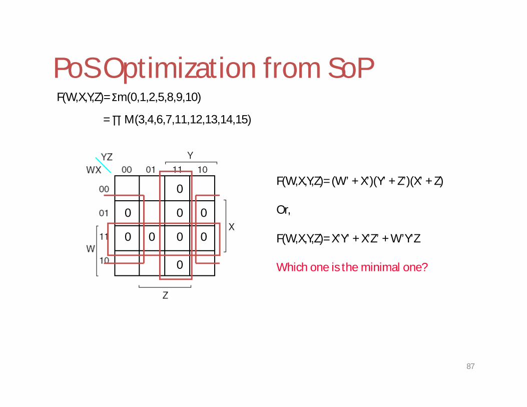
PoS Optimization from SoPF(W,X,Y,Z)= Σm(0,1,2,5,8,9,10)
= ∏ M(3,4,6,7,11,12,13,14,15)
0
0 00
0
0 0 0 0
F(W,X,Y,Z)= (W’ + X’)(Y’ + Z’)(X’ + Z)
Or,
F(W,X,Y,Z)= X’Y’ + X’Z’ + W’Y’Z
Which one is the minimal one?

88
SoP Optimization from PoSF(W,X,Y,Z)= ∏ M(0,2,3,4,5,6)
= Σm(1,7,8,9,10,11,12,13,14,15)
1
1
1 1 1 1
1 1 1 1
F(W,X,Y,Z)= W + XYZ + X’Y’Z

89
I don’t care!• You don’t always need all 2n input combinations in an n-variable function
– If you can guarantee that certain input combinations never occur– If some outputs aren’t used in the rest of the circuit
• We mark don’t-care outputs in truth tables and K-maps with Xs.
• Within a K-map, each X can be considered as either 0 or 1. You should pickthe interpretation that allows for the most simplification.
x y z f(x,y,z)0 0 0 00 0 1 10 1 0 X0 1 1 01 0 0 01 0 1 11 1 0 X1 1 1 1

90
Y 1 0 0 1 1 1 x 0
0 x 1 1 X
W 1 0 0 x
Z
Practice K-map • Find a MSP for
f(w,x,y,z) = m(0,2,4,5,8,14,15), d(w,x,y,z) = m(7,10,13)
This notation means that input combinations wxyz = 0111, 1010 and 1101(corresponding to minterms m7, m10 and m13) are unused.

91
Solutions for Practice K-map • Find a MSP for: f(w,x,y,z) = m(0,2,4,5,8,14,15),
d(w,x,y,z) = m(7,10,13)Y
1 11 1 x
x 1 1X
W1 x
Z
f(w,x,y,z)= x’z’ + w’xy’ + wxy

92
K-map Summary• K-maps are an alternative to algebra for simplifying
expressions– The result is a MSP/MPS, which leads to a minimal two-level circuit– It’s easy to handle don’t-care conditions– K-maps are really only good for manual simplification of small
expressions...
• Things to keep in mind:– Remember the correct order of minterms/maxterms on the K-map– When grouping, you can wrap around all sides of the K-map, and
your groups can overlap– Make as few rectangles as possible, but make each of them as large
as possible. This leads to fewer, but simpler, product terms– There may be more than one valid solution
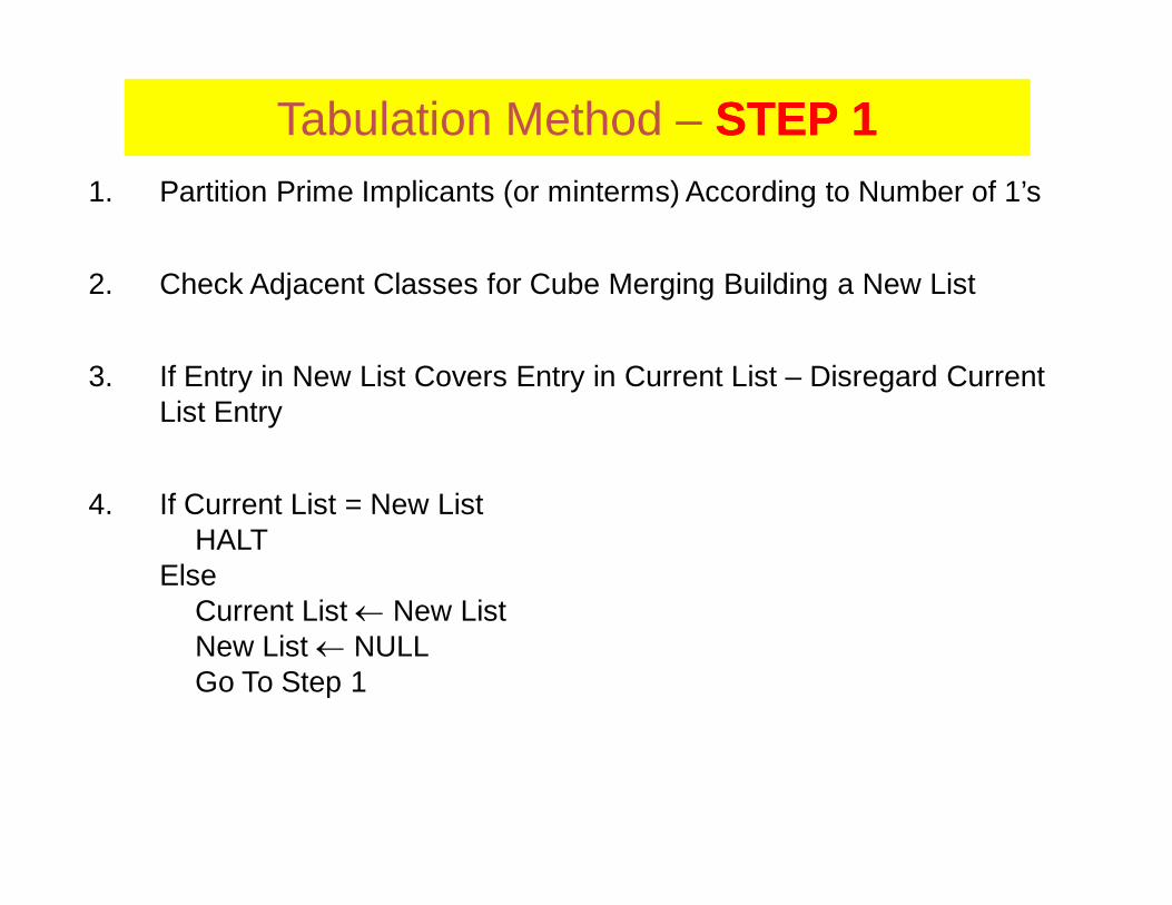
Tabulation Method – STEP 1STEP 11. Partition Prime Implicants (or minterms) According to Number of 1’s
2. Check Adjacent Classes for Cube Merging Building a New List
3. If Entry in New List Covers Entry in Current List – Disregard Current List Entry
4. If Current List = New ListHALT
ElseCurrent List New ListNew List NULLGo To Step 1

STEP 1 - EXAMPLE
f on = {m0, m1, m2, m3, m5, m8, m10, m11, m13, m15} = (0, 1, 2, 3, 5, 8, 10, 11, 13, 15)
Minterm Cube 0 0 0 0 0 1 0 0 0 1 2 0 0 1 0 8 1 0 0 0 3 0 0 1 1 5 0 1 0 1
10 1 0 1 0 11 1 0 1 1 13 1 1 0 1 15 1 1 1 1

STEP 1 - EXAMPLE
f on = {m0, m1, m2, m3, m5, m8, m10, m11, m13, m15} = (0, 1, 2, 3, 5, 8, 10, 11, 13, 15)
Minterm Cube 0 0 0 0 0 1 0 0 0 1 2 0 0 1 0 8 1 0 0 0 3 0 0 1 1 5 0 1 0 1
10 1 0 1 0 11 1 0 1 1 13 1 1 0 1 15 1 1 1 1
Minterm Cube 0,1 0 0 0 - 0,2 0 0 - 0 0,8 - 0 0 0 1,3 0 0 - 1 1,5 0 - 0 1 2,3 0 0 1 -
2,10 - 0 1 0 8,10 1 0 - 0 3,11 - 0 1 1 5,13 - 1 0 1
10,11 1 0 1 - 11,15 1 - 1 1 13,15 1 1 - 1
Minterm Cube 0,1,2,3 0 0 - -
0,8,2,10 - 0 - 0 2,3,10,11 - 0 1 -

STEP 1 - EXAMPLE
f on = {m0, m1, m2, m3, m5, m8, m10, m11, m13, m15} = (0, 1, 2, 3, 5, 8, 10, 11, 13, 15)
Minterm Cube 0 0 0 0 0 1 0 0 0 1 2 0 0 1 0 8 1 0 0 0 3 0 0 1 1 5 0 1 0 1
10 1 0 1 0 11 1 0 1 1 13 1 1 0 1 15 1 1 1 1
Minterm Cube 0,1 0 0 0 - 0,2 0 0 - 0 0,8 - 0 0 0 1,3 0 0 - 1 1,5 0 - 0 1 PI=D 2,3 0 0 1 -
2,10 - 0 1 0 8,10 1 0 - 0 3,11 - 0 1 1 5,13 - 1 0 1 PI=E 10,11 1 0 1 - 11,15 1 - 1 1 PI=F 13,15 1 1 - 1 PI=G
Minterm Cube 0,1,2,3 0 0 - - PI=A
0,8,2,10 - 0 - 0 PI=C 2,3,10,11 - 0 1 - PI=B
f on = {A,B,C,D,E,F,G} = {00--, -01-, -0-0, 0-01, -101, 1-11, 11-1}

STEP 2 – Construct Cover Table
• PIs Along Vertical Axis (in order of # of literals)• Minterms Along Horizontal Axis
0 1 2 3 5 8 10 11 13 15 A x x x x B x x x x C x x x x D x x E x x F x x G x x
NOTE: Table 4.2 in book is incomplete

STEP 2 – Finding the Minimum Cover• Extract All Essential Prime Implicants, EPI• EPIs are the PI for which a Single x Appears in a Column
0 1 2 3 5 8 10 11 13 15 A x x x x B x x x x C x x x x D x x E x x F x x G x x
• C is an EPI so: f on={C, ...}
• Row C and Columns 0, 2, 8, and 10 can be Eliminated Giving Reduced Cover Table
• Examine Reduced Table for New EPIs
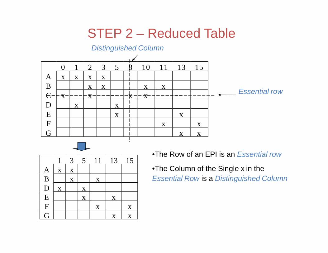
STEP 2 – Reduced Table
0 1 2 3 5 8 10 11 13 15 A x x x x B x x x x C x x x x D x x E x x F x x G x x
1 3 5 11 13 15 A x x B x x D x x E x x F x x G x x
Essential row
Distinguished Column
•The Row of an EPI is an Essential row
•The Column of the Single x in the Essential Row is a Distinguished Column

Row and Column DominanceRow and Column Dominance• If Row P has x’s Everywhere Row Q Does
Then Q Dominates P if P has fewer x’s
• If Column i has x’s Everywhere j DoesThen j Dominates i if i has fewer x’s
• If Row P is equal to Row Q and Row Q does not cost more than Row P, eliminate Row P, or if Row P is dominated by Row Q and Row Q Does not cost more than Row P, eliminate Row P
• If Column i is equal to Column j, eliminate Column i or if Column idominates Column j, eliminate Column i

STEP 3 – The Reduced Cover Table• Initially, Columns 0, 2, 8 and 10 Removed
1 3 5 11 13 15 A x x B x x D x x E x x F x x G x x
• No EPIs are Present • No Row Dominance Exists• No Column Dominance Exists• This is Cyclic Cover Table• Must Solve Exactly OR Use a Heuristic

NAND Function Implementation
• NAND gates can implement a simplified Sum-ofProducts form. Constructing two level NAND-NAND gate circuits
The first level is two 2-input NAND gates using ANDInvert. The second level is one 2-input NAND gate using Invert-OR. Using the NAND relationship, we

Logic Family Characteristics
• Complementary metal oxide semiconductor (CMOS)– most widely used family for large-scale devices– combines high speed with low power consumption– usually operates from a single supply of 5 – 15 V– excellent noise immunity of about 30% of supply voltage– can be connected to a large number of gates (about 50)– many forms – some with tPD down to 1 ns– power consumption depends on speed (perhaps 1 mW)

NAND Implementation (Cont.)
In the implementation, note that the bubbles are on opposite ends of the same line. Thus, they can be combined and deleted:
This form of the implementation is the Sum-of-Products form.

NOR Gates
The basic positive logic NOR gate (Not-OR) is denoted by the following symbol:
This is called the OR-Invert, since it is logically an OR function followed by an invert. By DeMorgan's Law we have the following Invert-AND symbol for a NOR gate:

General Implementations (Cont.)Given a two level implementation desired, use the previous transfromations
to get it into one of the below forms. Then follow the steps to transform the function to the desired form:

Multi-level NAND Implementations
• Add inverters in two-level implementation into the cost picture
• Attempt to “combine” inverters to reduce the term count
• Attempt to reduce literal + tem count by factoring expression into POSOP or SOPOS

• Transistor-transistor logic (TTL)– based on bipolar transistors– one of the most widely used families for small- and
medium-scale devices – rarely used for VLSI– typically operated from 5V supply– typical noise immunity about 1 – 1.6 V– many forms, some optimised for speed, power, etc.– high speed versions comparable to CMOS (~ 1.5 ns)– low-power versions down to about 1 mW/gate

• Emitter-coupled logic (ECL)– based on bipolar transistors, but removes
problems of storage time by preventing the transistors from saturating
– very fast operation - propagation delays of 1ns or less
– high power consumption, perhaps 60 mW/gate– low noise immunity of about 0.2-0.25 V– used in some high speed specialist applications,
but now largely replaced by high speed CMOS

A Comparison of Logic Families
Parameter CMOS TTL ECL
Basic gate NAND/NOR NAND OR/NOR
Fan-out >50 10 25
Power per gate (mW) 1 @ 1 MHz 1 - 22 4 - 55
Noise immunity Excellent Very good Good
tPD (ns) 1 - 200 1.5 – 33 1 - 4

Complementary Metal Oxide Semiconductor
• A CMOS inverter

• CMOS gates

• CMOS logic levels and noise immunity

Transistor-Transistor Logic
• Discrete TTL inverter and NAND gate circuits
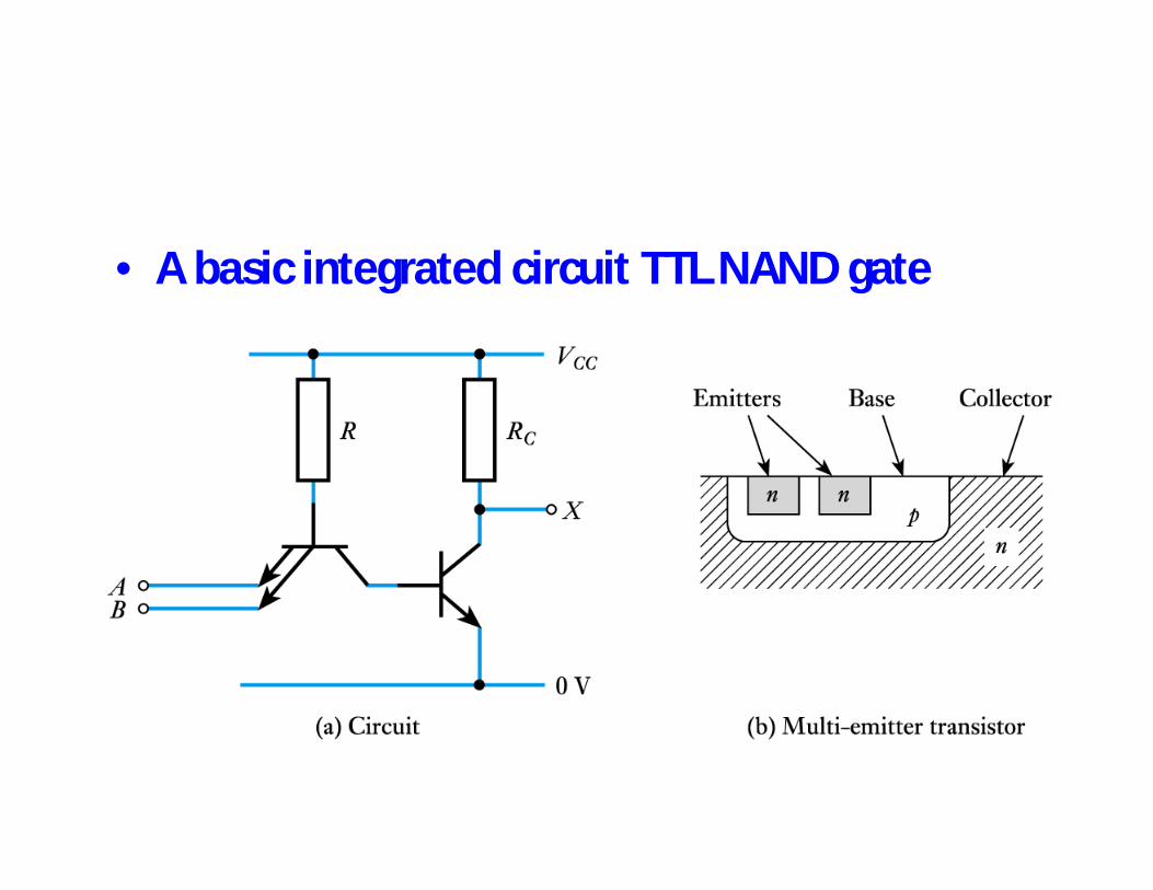
• A basic integrated circuit TTL NAND gate

• A standard TTL NAND gate

• A TTL NAND gate with open collector output

119
Combinational Logic
• Logic circuits for digital systems may be combinationalor sequential.
• A combinational circuit consists of input variables, logic gates, and output variables.

120
Analysis procedureTo obtain the output Boolean functions from a logic diagram, proceed as follows:
1. Label all gate outputs that are a function of input variables with arbitrary symbols. Determine the Boolean functions for each gate output.
2. Label the gates that are a function of input variables and previously labeled gates with other arbitrary symbols. Find the Boolean functions for these gates.
3. Repeat the process outlined in step 2 until the outputs of the circuit are obtained.
4. By repeated substitution of previously defined functions, obtain the output Boolean functions in terms of input variables.

121
ExampleF2 = AB + AC + BC; T1 = A + B + C; T2 = ABC; T3 = F2’T1; F1 = T3 + T2
F1 = T3 + T2 = F2’T1 + ABC = A’BC’ + A’B’C + AB’C’ + ABC

122
Derive truth table from logic diagram
• We can derive the truth table in Table 4-1 by using the circuit of Fig.4-2.

123
Design procedure1. Table4-2 is a Code-Conversion example, first, we can
list the relation of the BCD and Excess-3 codes in the truth table.

124
Karnaugh map2. For each symbol of the Excess-3 code, we use 1’s to
draw the map for simplifying Boolean function.
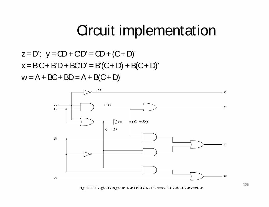
125
Circuit implementationz = D’; y = CD + C’D’ = CD + (C + D)’x = B’C + B’D + BC’D’ = B’(C + D) + B(C + D)’w = A + BC + BD = A + B(C + D)

126
Binary Adder-Subtractor• A combinational circuit that performs the addition of two bits is
called a half adder.• The truth table for the half adder is listed below:
S = x’y + xy’C = xy
S: SumC: Carry

127
Implementation of Half-Adder

128
Full-Adder• One that performs the addition of three bits(two
significant bits and a previous carry) is a full adder.

129
Simplified Expressions
S = x’y’z + x’yz’ + xy’z’ + xyzC = xy + xz + yz
C

130
Full adder implemented in SOP

131
Another implementation• Full-adder can also implemented with two half adders
and one OR gate (Carry Look-Ahead adder).S = z ⊕ (x ⊕ y)
= z’(xy’ + x’y) + z(xy’ + x’y)’= xy’z’ + x’yz’ + xyz + x’y’z
C = z(xy’ + x’y) + xy = xy’z + x’yz + xy

Half SubtractorTruth table
Logic Circuit

Full Subtractor

Full Subtractor

135
Binary adder• This is also called
Ripple Carry Adder ,because of the construction with full adders are connected in cascade.

136
Carry Propagation
• Fig.4-9 causes a unstable factor on carry bit, and produces a longest propagation delay.
• The signal from Ci to the output carry Ci+1, propagates through an AND and OR gates, so, for an n-bit RCA, there are 2n gate levels for the carry to propagate from input to output.

137
Carry Propagation
• Because the propagation delay will affect the output signals on different time, so the signals are given enough time to get the precise and stable outputs.
• The most widely used technique employs the principle of carry look-ahead to improve the speed of the algorithm.
138
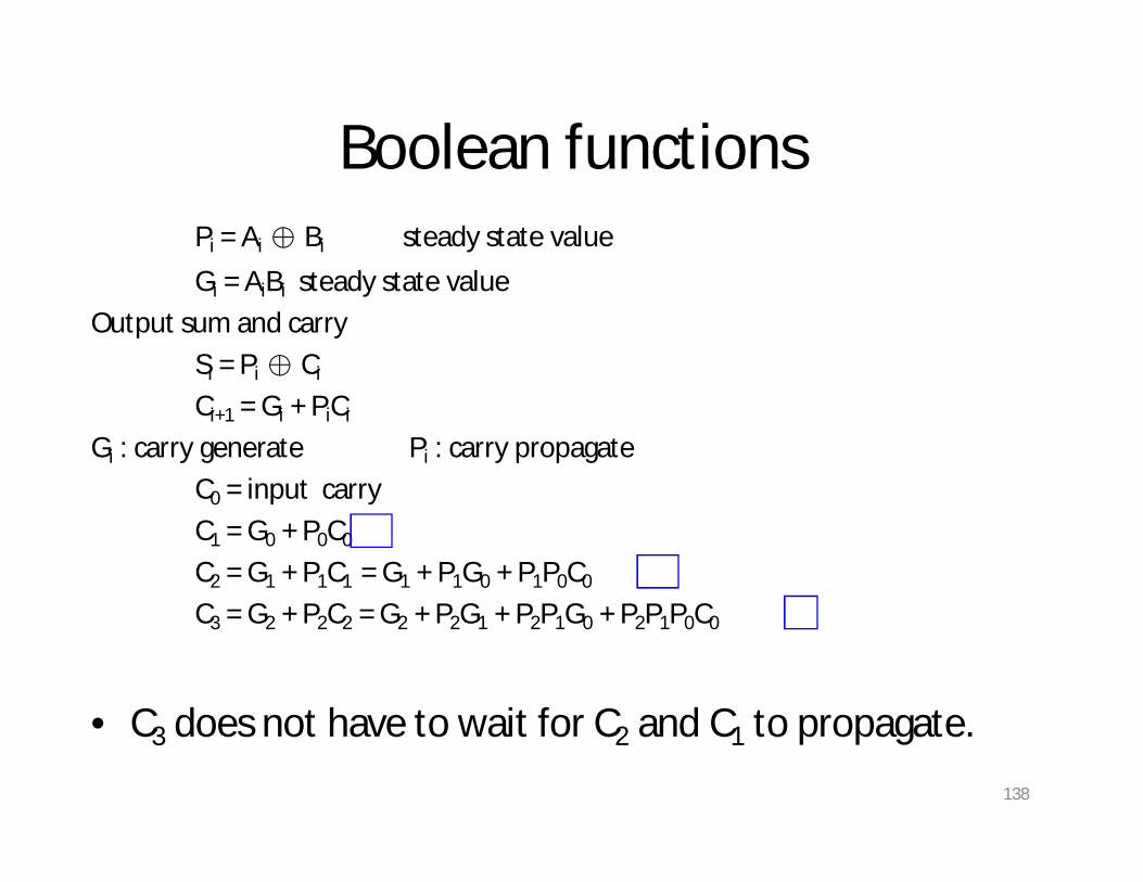
Boolean functionsPi = Ai ⊕ Bi steady state valueGi = AiBi steady state value
Output sum and carrySi = Pi ⊕ Ci
Ci+1 = Gi + PiCi
Gi : carry generate Pi : carry propagateC0 = input carryC1 = G0 + P0C0
C2 = G1 + P1C1 = G1 + P1G0 + P1P0C0
C3 = G2 + P2C2 = G2 + P2G1 + P2P1G0 + P2P1P0C0
• C3 does not have to wait for C2 and C1 to propagate.

139
Logic diagram of carry look-ahead generator
• C3 is propagated at the same time as C2 and C1.

140
4-bit adder with carry lookahead
• Delay time of n-bit CLAA = XOR + (AND + OR) + XOR

141
Binary subtractorM = 1subtractor ; M = 0adder
142
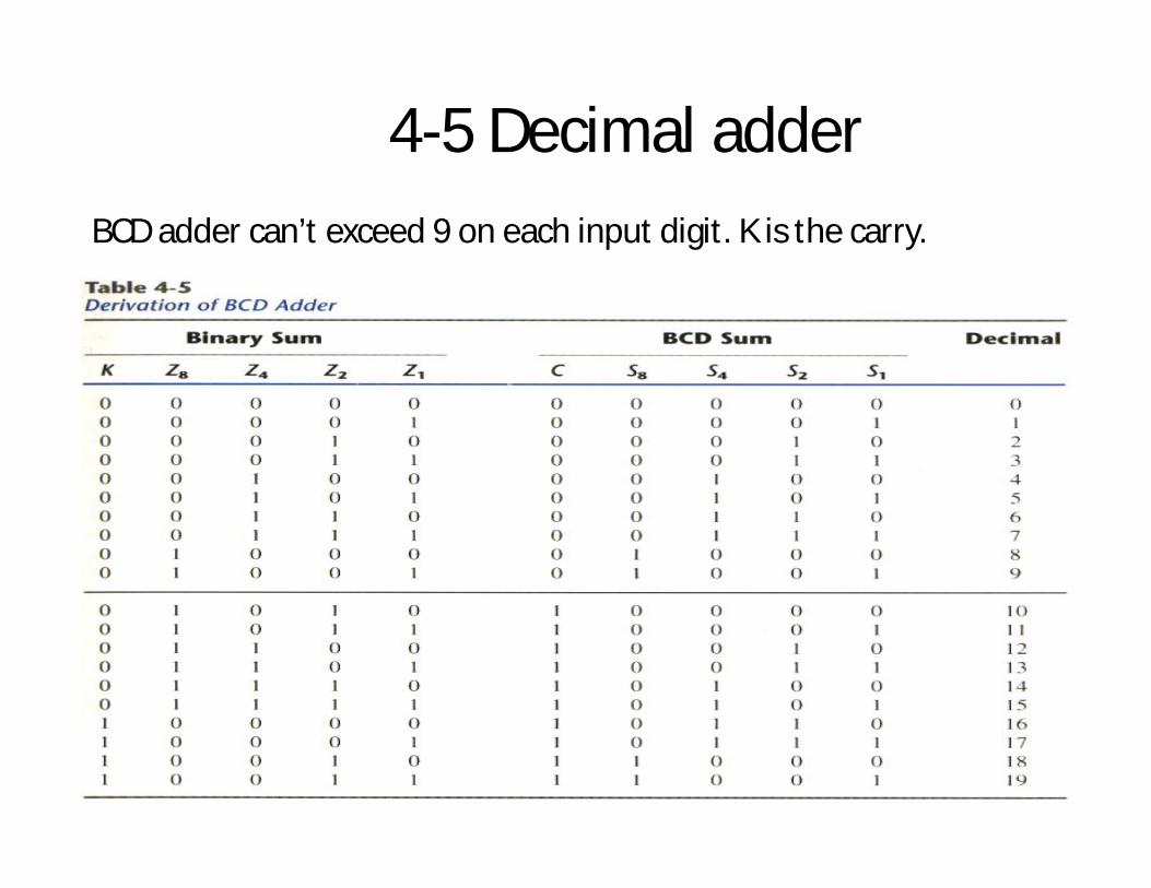
4-5 Decimal adderBCD adder can’t exceed 9 on each input digit. K is the carry.

143
Rules of BCD adder• When the binary sum is greater than 1001, we obtain a non-valid
BCD representation.
• The addition of binary 6(0110) to the binary sum converts it to the correct BCD representation and also produces an output carry as required.
• To distinguish them from binary 1000 and 1001, which also have a 1 in position Z8, we specify further that either Z4 or Z2 must have a 1.
C = K + Z8Z4 + Z8Z2

144
Implementation of BCD adder• A decimal parallel
adder that adds n decimal digits needs n BCD adder stages.
• The output carry from one stage must be connected to the input carry of the next higher-order stage.
If =1
0110

145
4-6. Binary multiplier• Usually there are more bits in the partial products and it is necessary to use full
adders to produce the sum of the partial products.
And

146
4-bit by 3-bit binary multiplier
• For J multiplier bits and K multiplicand bits we need (J X K) AND gates and (J − 1) K-bit adders to produce a product of J+K bits.
• K=4 and J=3, we need 12 AND gates and two 4-bit adders.

147
Magnitude comparator• The equality relation of each pair
of bits can be expressed logically with an exclusive-NOR function as:
A = A3A2A1A0 ; B = B3B2B1B0
xi=AiBi+Ai’Bi’ for i = 0, 1, 2, 3
(A = B) = x3x2x1x0

148
Magnitude comparator• We inspect the relative magnitudes
of pairs of MSB. If equal, we compare the next lower significant pair of digits until a pair of unequal digits is reached.
• If the corresponding digit of A is 1 and that of B is 0, we conclude that A>B.
(A>B)=A3B’3+x3A2B’2+x3x2A1B’1+x3x2x1A0B’0(A<B)=A’3B3+x3A’2B2+x3x2A’1B1+x3x2x1A’0B0
149
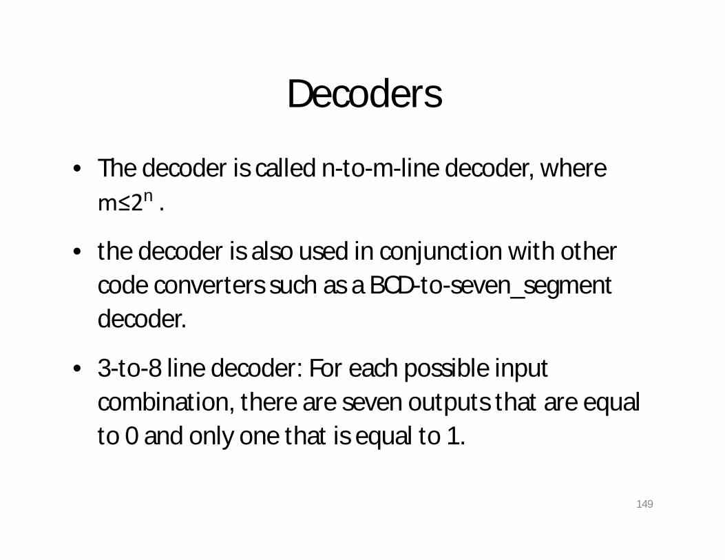
Decoders
• The decoder is called n-to-m-line decoder, where m≤2n .
• the decoder is also used in conjunction with other code converters such as a BCD-to-seven_segment decoder.
• 3-to-8 line decoder: For each possible input combination, there are seven outputs that are equal to 0 and only one that is equal to 1.

150
Implementation and truth table
151
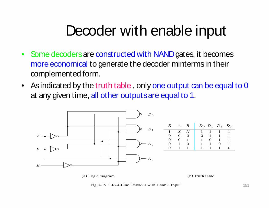
Decoder with enable input• Some decoders are constructed with NAND gates, it becomes
more economical to generate the decoder minterms in their complemented form.
• As indicated by the truth table , only one output can be equal to 0at any given time, all other outputs are equal to 1.
152
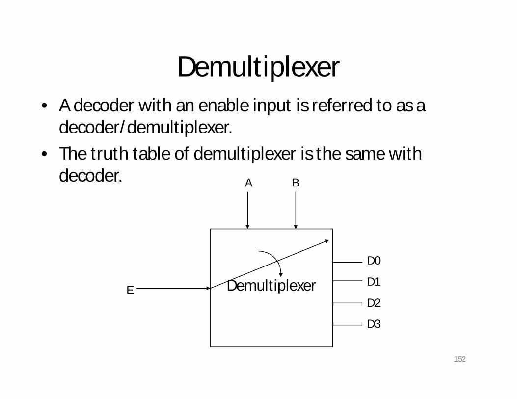
Demultiplexer• A decoder with an enable input is referred to as a
decoder/demultiplexer.• The truth table of demultiplexer is the same with
decoder.
Demultiplexer
D0
D1
D2
D3
E
A B

153
3-to-8 decoder with enable implement the 4-to-16 decoder

154
Implementation of a Full Adder with a Decoder
• From table 4-4, we obtain the functions for the combinational circuit in sum of minterms:
S(x, y, z) = ∑(1, 2, 4, 7)C(x, y, z) = ∑(3, 5, 6, 7)

155
4-9. Encoders• An encoder is the inverse operation of a decoder.• We can derive the Boolean functions by table 4-7
z = D1 + D3 + D5 + D7
y = D2 + D3 + D6 + D7
x = D4 + D5 + D6 + D7

156
Priority encoder
• If two inputs are active simultaneously, the output produces an undefined combination. We can establish an input priorityto ensure that only one input is encoded.
• Another ambiguity in the octal-to-binary encoder is that an output with all 0’s is generated when all the inputs are 0; the output is the same as when D0 is equal to 1.
• The discrepancy tables on Table 4-7 and Table 4-8 can resolve aforesaid condition by providing one more output to indicate that at least one input is equal to 1.

157
Priority encoderV=0no valid inputsV=1valid inputs
X’s in output columns represent don’t-care conditionsX’s in the input columns are useful for representing a truth table in condensed form. Instead of listing all 16 minterms of four variables.

158
4-input priority encoder
• Implementation of table 4-8
x = D2 + D3
y = D3 + D1D’2V = D0 + D1 + D2 + D3
0
00
0

159
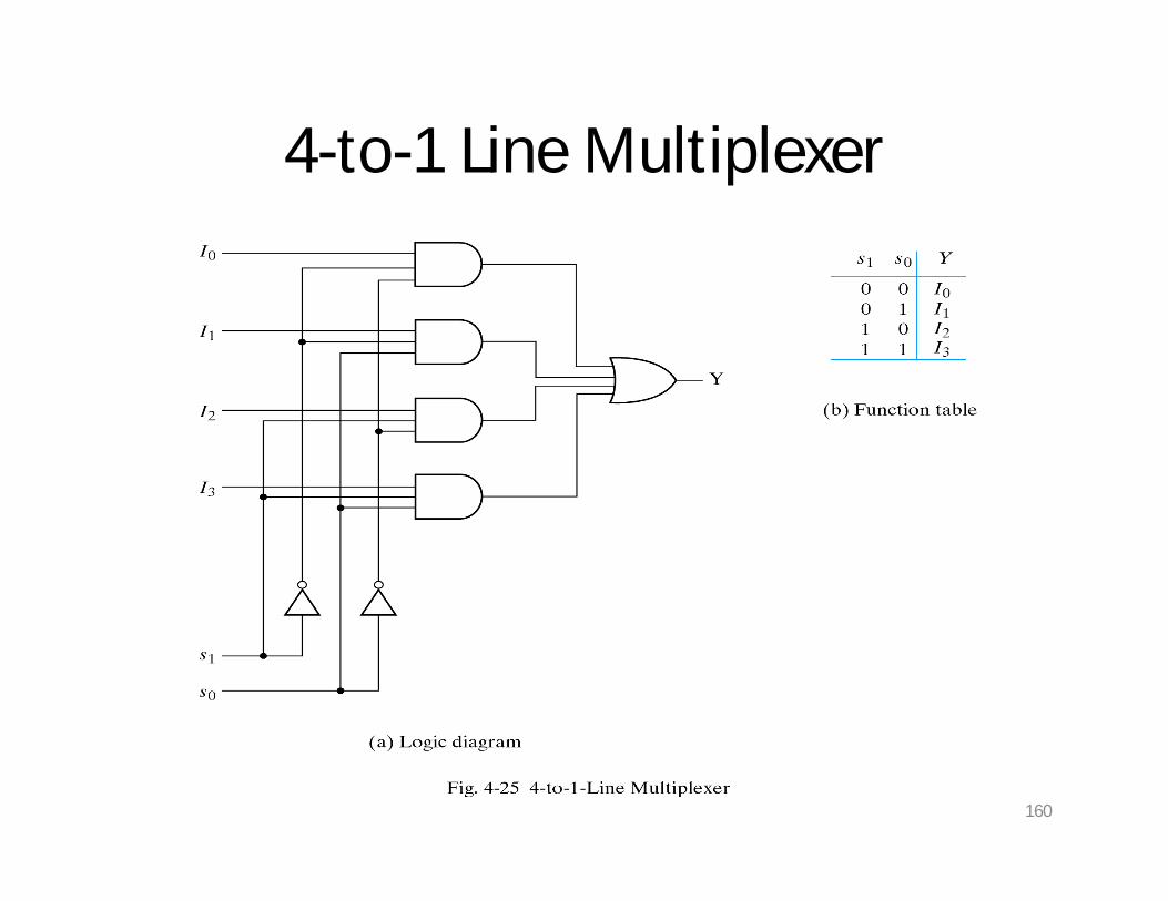
4-10. Multiplexers
S = 0, Y = I0 Truth Table S Y Y = S’I0 + SI1
S = 1, Y = I1 0 I0
1 I1
160
4-to-1 Line Multiplexer
161
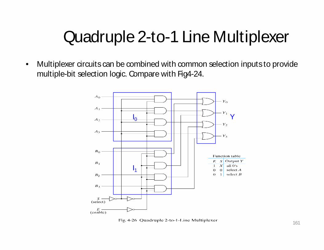
Quadruple 2-to-1 Line Multiplexer• Multiplexer circuits can be combined with common selection inputs to provide
multiple-bit selection logic. Compare with Fig4-24.
I0
I1
Y

162
Boolean function implementation
• A more efficient method for implementing a Boolean function of n variables with a multiplexer that has n-1 selection inputs.
F(x, y, z) = (1,2,6,7)
163
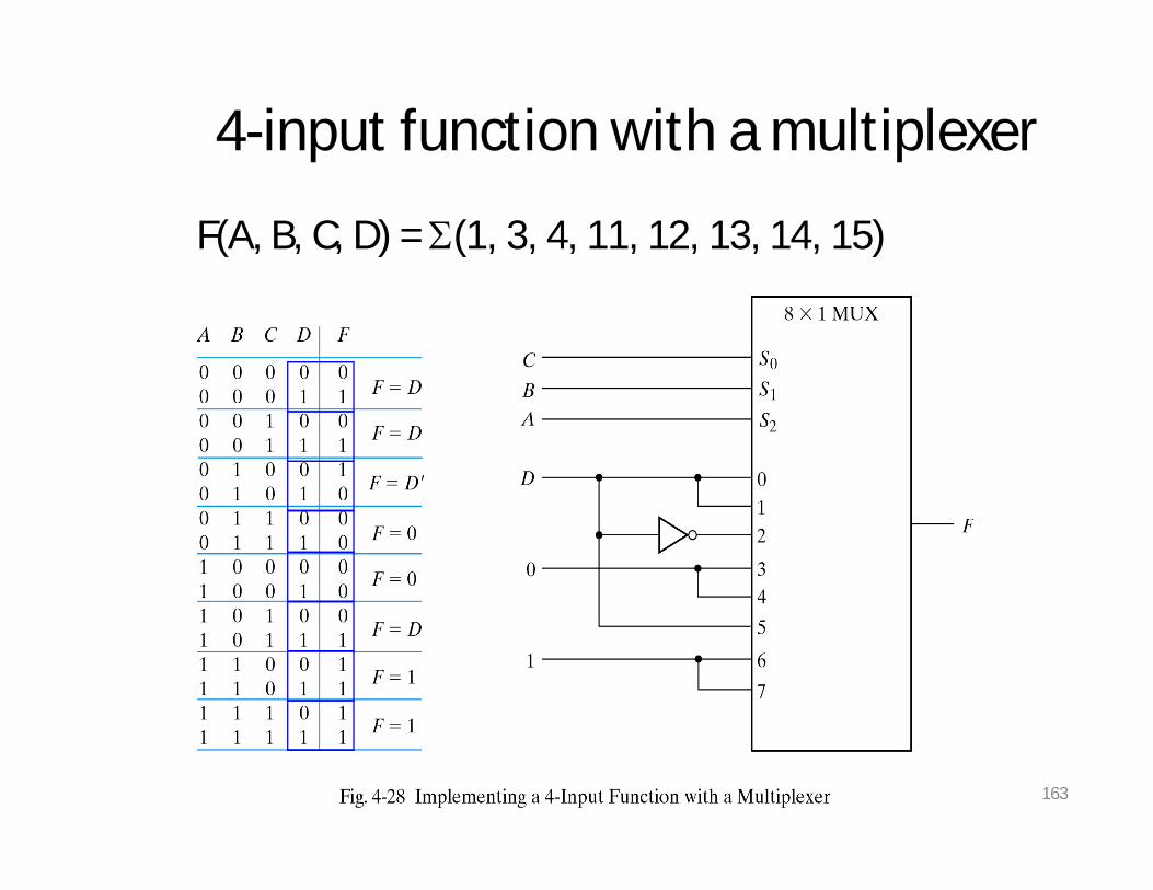
4-input function with a multiplexer
F(A, B, C, D) = (1, 3, 4, 11, 12, 13, 14, 15)

164
Three-State Gates• A multiplexer can be constructed with three-state gates.
165
Sequential Circuits
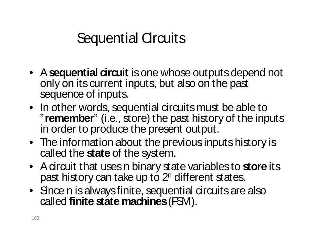
• A sequential circuit is one whose outputs depend not only on its current inputs, but also on the past sequence of inputs.
• In other words, sequential circuits must be able to ”remember” (i.e., store) the past history of the inputs in order to produce the present output.
• The information about the previous inputs history is called the state of the system.
• A circuit that uses n binary state variables to store its past history can take up to 2n different states.
• Since n is always finite, sequential circuits are also called finite state machines (FSM).

166
In short, sequential circuits are …
• circuits consisting of ordinary gates and feedback loops
X1X2•••
Xn
switchingnetwork
Z1Z2•••
Zn

167
"remember"
"load""data" "stored value"
"0"
"1"
"stored value"
The simplest sequential circuit
• Two inverters and a feedback loop form a “static” storage cell– The cell will hold value as long as it has power applied
• How to get a new value into the storage cell?– selectively break feedback path– load new value into cell D latch
(= state)bistable cell

168
Latches and Flip-Flops
• The two most popular varieties of storage cells used to build sequential circuits are: latches and flip-flops.– Latch: level sensitive storage element– Flip-Flop: edge triggered storage element
• Common examples of latches: S-R latch, \S-\R latch, D latch (= gated D latch)
• Common examples of flip-flops: D-FF, D-FF with enable, Scan-FF, JK-FF, T-FF

169
S-R (Set-Reset) Latch
S-R latch: similar to inverter pair, with capability to force output to 0 (reset=1) or 1 (set=1)
RS
Q
X Y NOR0 0 10 1 01 0 01 1 0
QN

170
S-R latch operation
SR
QN
Q00
0=
=1
SR
QN
Q10
0=
=0
=10=
SR
QN
Q00 =1
=0
=1
SR
QN
Q01 =1
=1
=0

171
S-R latch operation (cont’d)
Both Q and QN are 0 at the same time
Race
(hold)(reset)(set)(forbidden)

172
Improper S-R latch operation
Reset Hold Set SetReset Race
R
S
Q
QN
QN Theoretically the circuit starts to oscillate

173
S(t) R(t) Q(t) Q(t+)0 0 0 00 0 1 10 1 0 00 1 1 01 0 0 11 0 1 11 1 0 X1 1 1 X
hold
reset
set
not allowed
next state equation:Q(t+) = S(t) + R’(t) Q(t)
R-S latch analysis
• Break feedback path
R
S
Q
QN
Q(t+)
R(t)S(t)
Q(t)
0 0
1 0
X 1
X 1Q(t)
R(t)
S(t)
Q+ = Q* = S + R’ Qa.k.a. characteristic equation

174
S-R Latch
RNSN
Q(t)
X 1
X 1
0 0
1 0Q(t)
RN(t)
SN(t)
SN(t) RN(t) Q(t) Q(t+)1 1 0 01 1 1 11 0 0 01 0 1 00 1 0 10 1 1 10 0 0 X0 0 1 X
hold
reset
set
not allowed
next state equation:Q(t+) = S’(t) + R(t) Q(t)
Q+ = Q* = S’ + R Q

175
D Latch (= Transparent Latch)
=

176
D-Latch Timing Parameters
• The D Latch eliminates the S=R=1 problem of the SR latch• However, violations of setup and hold time still cause metastability

177
Clock signals
• Clocks are regular periodic signals used to specify state changes

178
D Flip-Flop (positive edge triggered)
Notice: the little triangle !
Functional Table Truth TableMore compact
Truth Table
D Q+
0 01 1
Next state equation:
CLK
D
Q
inputs sampled on rising edge; outputs change after rising edge

179
Setup and hold times for an edge-triggered DFF

180
Minimum clock period T ?
Example with T = 9 ns
tpINV = 2 nstpFF = 5 nstsuFF = 3 ns
Example with T = 15 ns
T = 9 ns T = 15 ns

181
Minimum clock period T ? (cont’d)
tpINV = 2 nstpFF = 5 nstsuFF = 3 ns
Tmin = 10 ns
Observation:thFF doesn’t affect this calculation

182
D Flip-Flop (negative edge triggered)
inputs sampled on falling edge; outputs change after falling edge

183
DFF with asynchronous preset and clear
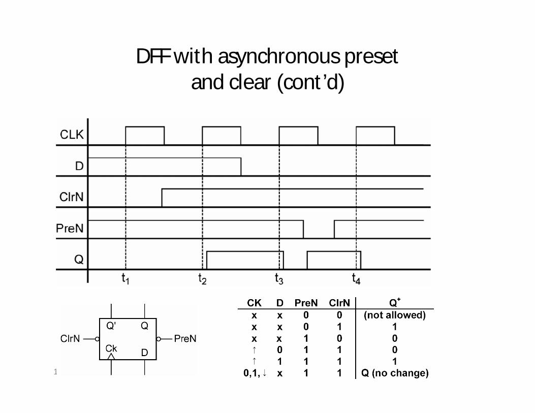
184
DFF with asynchronous preset and clear (cont’d)
185
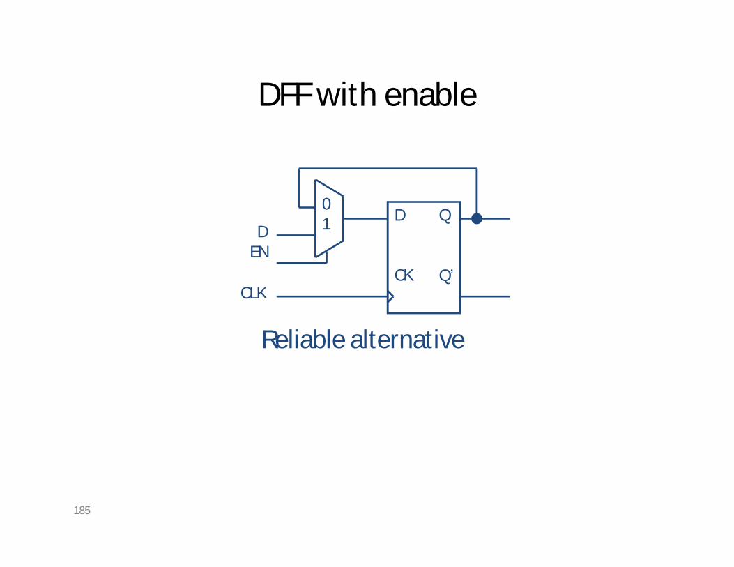
DFF with enable
D
CK
01 Q
Q’
DEN
CLK
Reliable alternative

186
DFF with enable (cont’d)

187
JK Flip Flop (rising edge triggered)
=
Functional Table Truth Table More Compact Truth Table
J K Q+
0 0 Q0 1 01 0 11 1 Q’
Next state equation:

188
Summary of latches and flip flops

189
behavior is the same unless input changeswhile the clock is high
D Q
CLK
positiveedge-triggered
flip-flop
D QG
CLK
transparent(level-sensitive)
latch
D
CLK
QFF
Qlatch
Comparison of latches and flip-flops
QFF
Qlatch

190
Synchronous Sequential Circuit Analysis

191
Synchronous Sequential Circuit• State Memory – A set of n edge-triggered flip-flops that
store the current state of the machine – All flip-flops are triggered from the same master clock signal – All change state together
• Combinational circuit– Next state logic– Output logic – Mealy and Moore
Combinationalcircuit
Inputs
State Memory
Outputs
Clock
CurrentState
NextState

192
Mealy Model
next state = F (current state, inputs)
outputs = G (current state, inputs)
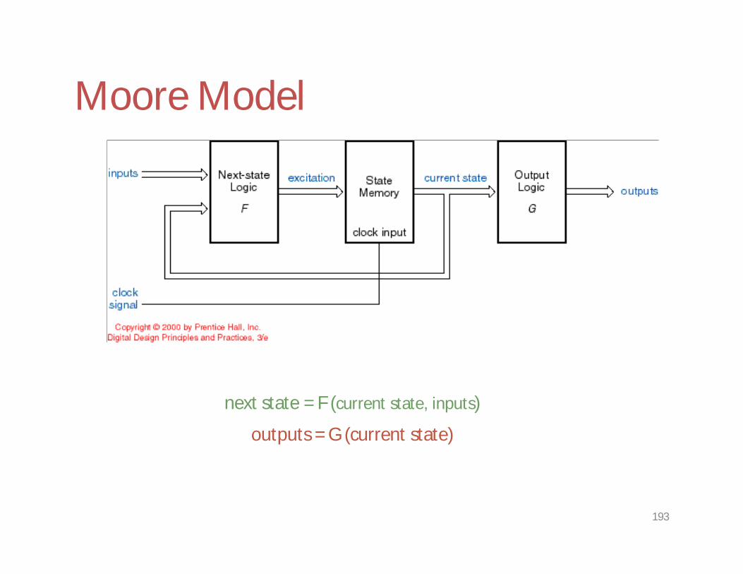
193
Moore Model
next state = F (current state, inputs)
outputs = G (current state)

194
Analysis - Goals• Characterize as Mealy or Moore machine• Determine next state equations, i.e., find the function F
– next state = F (current state, inputs)• Determine output equations
– Meally: outputs = F (current state, inputs), or– Moore: outputs = F (current state)
• Express as machine behavior– State table, or – State diagram
• Formulate English description of machine behavior

195
An example sequential circuit
• A sequential circuit with two JK flip-flops
• State or memory: Q1Q0
• One input: X; One output: Z
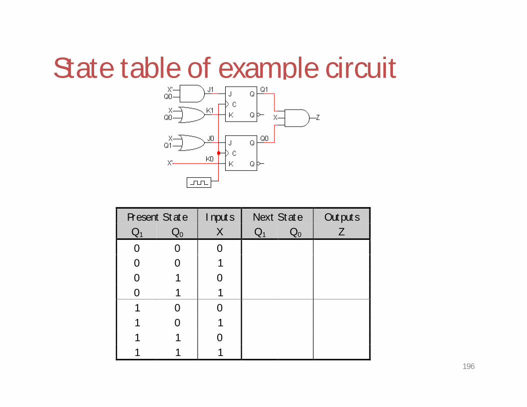
196
State table of example circuit
Present State Inputs Next State OutputsQ1 Q0 X Q1 Q0 Z0 0 00 0 10 1 00 1 11 0 01 0 11 1 01 1 1

197
Output Equations• From the diagram, you can see that
Z = Q1Q0X
Mealy model circuit !!!
Present State Inputs Next State OutputsQ1 Q0 X Q1 Q0 Z0 0 0 00 0 1 00 1 0 00 1 1 01 0 0 01 0 1 01 1 0 01 1 1 1

198
Next State Equations – Q(t+1)• Find the flip-flop input equations/excitation equations• Substitute excitation equations in the flip-flop’s characteristic equation
J1 = X’ Q0
K1 = X + Q0
J0 = X + Q1
K0 = X’

199
Next State Equations – Q(t+1)
• Next state equations:
– Q1(t+1) = K1’Q1(t) + J1Q1’(t)= (X + Q0(t))’ Q1(t) + X’ Q0 (t) Q1’(t)= X’ (Q0(t)’ Q1(t) + Q0(t) Q1(t)’)= X’ (Q0(t) Q1(t))
– Q0(t+1) = K0’Q0(t) + J0Q0’(t)= X Q0(t) + (X + Q1(t)) Q0’(t)= X + Q0(t)’ Q1(t)
• Excitation equations:– J1 = X’ Q0 and K1 = X + Q0
– J0 = X + Q1 and K0 = X’
• Characteristic equation of the JK flip-flop:– Q(t+1) = K’Q(t) + JQ’(t)

200
State Table & Next State Equations• Q1(t+1) = X’ (Q0(t) Q1(t))
– Q1=0, Q0=0, X= 0 => Q1(t+1)= 0
• Q0(t+1) = X + Q0(t)’ Q1(t)
– Q1=0, Q0=0, X= 0 => Q0(t+1)= 0
Present State Inputs Next State OutputsQ1 Q0 X Q1 Q0 Z0 0 0 00 0 1 00 1 0 00 1 1 01 0 0 01 0 1 01 1 0 01 1 1 1
0 0

201
State Table & Next State Equations• Q1(t+1) = X’ (Q0(t) Q1(t))
– Q1=0, Q0=1, X= 1 => Q1(t+1)= 0
• Q0(t+1) = X + Q0(t)’ Q1(t)
– Q1=0, Q0=1, X= 1 => Q0(t+1)= 1
Present State Inputs Next State OutputsQ1 Q0 X Q1 Q0 Z0 0 0 00 0 1 00 1 0 00 1 1 01 0 0 01 0 1 01 1 0 01 1 1 1
0 0
0 1

202
State Table & Next State Equations• Q1(t+1) = X’ (Q0(t) Q1(t))
• Q0(t+1) = X + Q0(t)’ Q1(t)
Present State Inputs Next State OutputsQ 1 Q0 X Q1 Q0 Z0 0 0 0 0 00 0 1 0 1 00 1 0 1 0 00 1 1 0 1 01 0 0 1 1 01 0 1 0 1 01 1 0 0 0 01 1 1 0 1 1

203
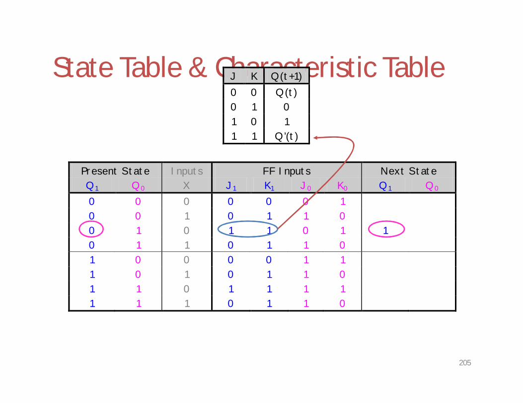
State Table & Characteristic Table• The general JK flip-flop characteristic equation is:
Q(t+1) = K’Q(t) + JQ’(t)• We can also determine the next state for each input/current
state combination directly from the characteristic table
J K Q(t+1) Operation0 0 Q(t) No change0 1 0 Reset1 0 1 Set1 1 Q’(t) Complement

204
State Table & Characteristic Table• With these equations, we can make a table showing J1, K1, J0 and K0
for the different combinations of present state Q1Q0 and input X
J1 = X’ Q0 J0 = X + Q1
K1 = X + Q0 K0 = X’Present State Inputs Flip-flop InputsQ1 Q0 X J1 K1 J0 K0
0 0 0 0 0 0 10 0 1 0 1 1 00 1 0 1 1 0 10 1 1 0 1 1 01 0 0 0 0 1 11 0 1 0 1 1 01 1 0 1 1 1 11 1 1 0 1 1 0
205
State Table & Characteristic Table
Present State Inputs FF Inputs Next State Q1 Q0 X J1 K1 J0 K0 Q1 Q0 0 0 0 0 0 0 1 0 0 1 0 1 1 0 0 1 0 1 1 0 1 1 0 1 1 0 1 1 0 1 0 0 0 0 1 1 1 0 1 0 1 1 0 1 1 0 1 1 1 1 1 1 1 0 1 1 0
J K Q(t+1) 0 0 Q(t) 0 1 0 1 0 1 1 1 Q’(t)
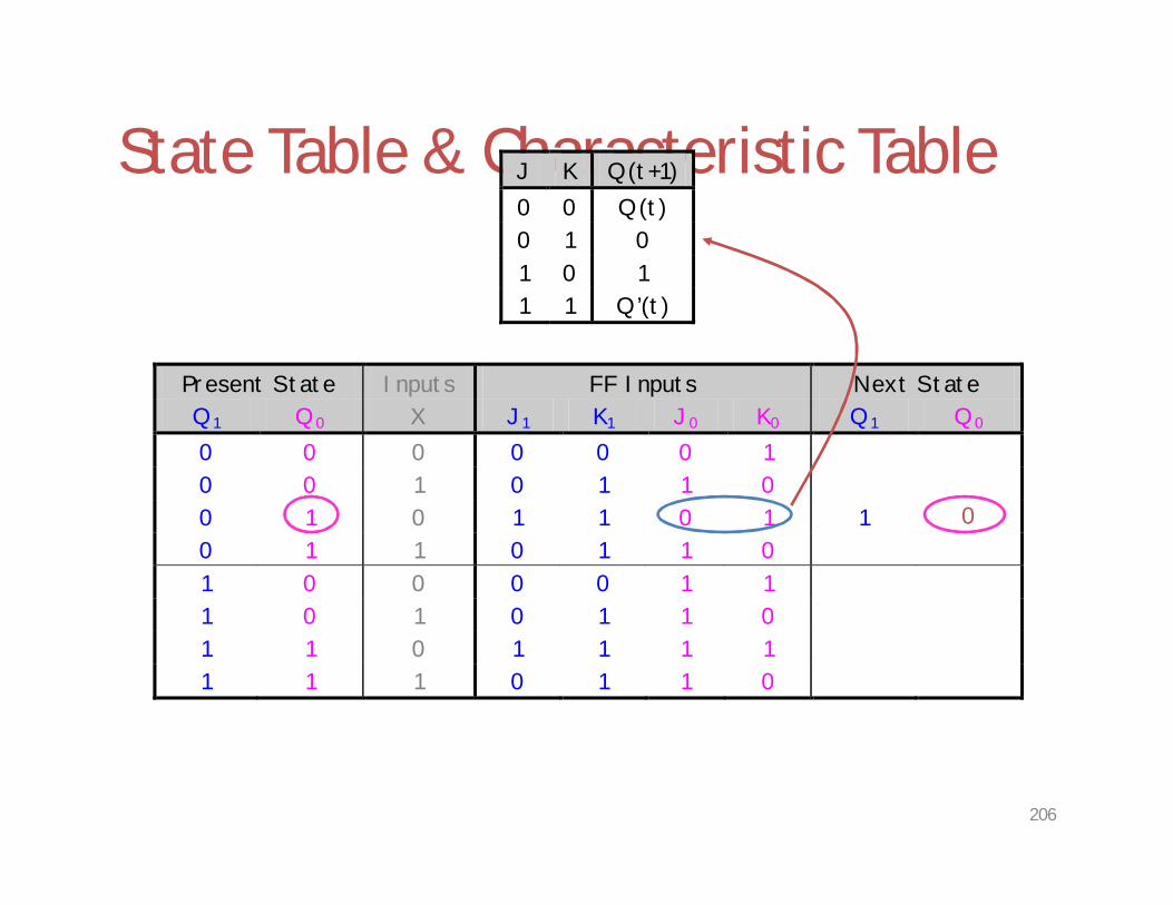
206
State Table & Characteristic Table
Present State Inputs FF Inputs Next State Q1 Q0 X J1 K1 J0 K0 Q1 Q0 0 0 0 0 0 0 1 0 0 1 0 1 1 0 0 1 0 1 1 0 1 1 0 1 1 0 1 1 0 1 0 0 0 0 1 1 1 0 1 0 1 1 0 1 1 0 1 1 1 1 1 1 1 0 1 1 0
J K Q(t+1) 0 0 Q(t) 0 1 0 1 0 1 1 1 Q’(t)
0

207
A different lookPresent State Inputs Next State Outputs
Q 1 Q0 X Q1 Q0 Z0 0 0 0 0 00 0 1 0 1 00 1 0 1 0 00 1 1 0 1 01 0 0 1 1 01 0 1 0 1 01 1 0 0 0 01 1 1 0 1 1
Present StateQ1 Q0
Next StateOutput
ZInput X= 0
Input X= 1
X= 0 X= 1
0 0 0 0 0 1 0 00 1 1 0 0 1 0 01 0 1 1 0 1 0 01 1 0 0 0 1 0 1

208
State diagrams (Mealy model)
Present State Inputs Next State OutputsQ1 Q0 X Q1 Q0 Z0 0 0 0 0 00 0 1 0 1 00 1 0 1 0 00 1 1 0 1 01 0 0 1 1 01 0 1 0 1 01 1 0 0 0 01 1 1 0 1 1
• We can also represent the state table graphically with a state diagram• A diagram corresponding to our example state table is shown below
00 01
1011
1/0
0/00/0
0/0
0/0 1/0
1/01/1
input output
state

209
Sizes of state diagrams
00 01
1011
1/0
0/00/0
0/0
0/0 1/0
1/01/1
• Always check the size of your state diagrams– If there are n flip-flops, there should be 2n nodes in the diagram– If there are m inputs, then each node will have 2m outgoing arrows
• In our example,– We have two flip-flops, and thus four states or nodes.– There is one input, so each node has two outgoing arrows.

210
Another Mealy Circuit

211
Excitation Equations
•• DD00 = EN’ = EN’ QQ00 ++ EN EN QQ00’’
•• DD11 = EN’ = EN’ QQ11 + EN + EN QQ11’ ’ QQ00 + EN + EN QQ11 QQ00’’

212
Next State/Output Equations
•• QQ00(t+1) = D(t+1) = D00 = EN’ = EN’ QQ00 ++ EN EN QQ00’’
•• QQ11(t+1) = D(t+1) = D11 = EN’ = EN’ QQ11 + EN + EN QQ11’ ’ QQ00 + EN + EN QQ11 QQ00’’
•• MAX= EN MAX= EN QQ11 QQ00

213
Mealy State Table
Present StateQ1 Q0
Next StateOutputMAX
Input EN= 0
Input EN= 1
X= 0 X= 1
0 0 0 0 0 1 0 00 1 0 1 1 0 0 01 0 1 0 1 1 0 01 1 1 1 0 0 0 1
•• QQ00(t+1) = D(t+1) = D00 = EN’ = EN’ QQ00 ++ EN EN QQ00’’
•• QQ11(t+1) = D(t+1) = D11 = EN’ = EN’ QQ11 + EN + EN QQ11’ ’ QQ00 + EN + EN QQ11 QQ00’’
•• MAX= EN MAX= EN QQ11 QQ00

214
Mealy State Diagram
Present StateQ1 Q0
Next StateOutputMAX
Input EN= 0
Input EN= 1
X= 0 X= 1
0 0 0 0 0 1 0 00 1 0 1 1 0 0 01 0 1 0 1 1 0 01 1 1 1 0 0 0 1

215
Moore CircuitX
Remove input connection to
output logic => Moore machine

216
Next State/Output Equations
•• QQ00(t+1) = D(t+1) = D00 = EN’ = EN’ QQ00 ++ EN EN QQ00’’
•• QQ11(t+1) = D(t+1) = D11 = EN’ = EN’ QQ11 + EN + EN QQ11’ ’ QQ00 + EN + EN QQ11 QQ00’’
•• MAX= MAX= QQ11 QQ00
X

217
Moore State Table
Present StateQ1 Q0
Next StateOutputMAXInput
EN= 0Input EN= 1
0 0 0 0 0 1 00 1 0 1 1 0 01 0 1 0 1 1 01 1 1 1 0 0 1
•• QQ00(t+1) = D(t+1) = D00 = EN’ = EN’ QQ00 ++ EN EN QQ00’’
•• QQ11(t+1) = D(t+1) = D11 = EN’ = EN’ QQ11 + EN + EN QQ11’ ’ QQ00 + EN + EN QQ11 QQ00’’
•• MAX= MAX= QQ11 QQ00
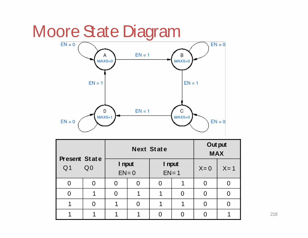
218
Moore State Diagram
Present StateQ1 Q0
Next StateOutputMAX
Input EN= 0
Input EN= 1
X= 0 X= 1
0 0 0 0 0 1 0 00 1 0 1 1 0 0 01 0 1 0 1 1 0 01 1 1 1 0 0 0 1

219
State Transitions
• MAX : Output of the Mealy circuit• MAXS : Output of the Moore circuit

Shift registerCircuit for simple shift register
Basic applications
Ring counters
Johnson counters
Pseudo-random binary sequences and encryptionReady-made shift registers are available as integrated circuits, such as the ’165
Conversion of data from serial to parallel and vice versaLarge-scale devices such as ‘universal asynchronous receiver transmitters’ (UARTs) are based on shift registers
Same functions available in microcontrollers (‘shift’ and ‘rotate’ instructions)

Basic shift registerA basic shift register is simply a chain of D flip-flops with a common clock.
D Q D Q D Q D Qserial input
serial output
clock
Each flip-flop transfers its D input to its Q output at a clock transition.• The effect is to transfer data along the register, one flip-flop per clock
cycle.
This type of register is called a serial input-serial output (SISO).
A B C D

Basic shift registerA basic shift register is simply a chain of D flip-flops with a common clock.
D Q D Q D Q D Qserial input01001110
serial output
clock
The table shows the contents of theregister after successive clock transitions.The assumption is that the register is initially clear.• The number of clock pulses needed to
fill the register is equal to the number of flip-flops used to make the register.
• This is a 4 bit register.
A B C D
cloc
k pu
lses
0 0 1 0 0
input QA QB QC QD
0 0 0 0 0
1 1 0 0 01 1 1 0 01 1 1 1 00 0 1 1 10 0 0 1 11 1 0 0 1

Timing for a shift register
clock
input
QA
QB
QC
QD
The pattern in successive flip-flops moves to the right with each clock cycle to shift the pattern into and out of the register.
tpd

Timing for a shift register
clock
input
QA
QB
QC
QD tpd
input QA QB QC
0 0 0 0111
111
011
001
QD
0 0 1 1 1
0000

Applications of a basic shift register1. Delay line — N stages delay the signal by N clock cycles
2. Multiplication and division by powers of 2, because this just requires a shift of the binary number (like multiplication or division by 10 in decimal)
Example: decimal 3 x 4 = 12 becomes 11 x 100 = 1100 in binary The
arithmetic logic unit (ALU) of a computer processor uses a shift
register for this purpose.
Warning: the ‘sense’ of a shift — left or right — is usually based on its effect on binary numbers written in the usual way. For example,11 → 1100 is called a left shift. This is clearer if both numbers are written with 8-bits as 00000011 → 00001100. Similarly, dividing by 2 such as 00010110 → 00001011 is a right shift.This is the opposite of what we usually draw in a counter circuit, with the least significant bit (LSB) on the left. Take care!
There is a ‘rotate’ operation where the output from the shift register is fed back to the beginning, usually through the ‘carry bit’.

Ring counterA shift register with its output fed back to its input forms a ring counter.
clock A B C D
D Q D Q D Q D Q
It is much harder to multiply a given frequency to obtain a higher frequency signal. A phase locked loop (PLL) is often used.
This can be used to generate an arbitrary binary pattern of length N, where N is the number of stages in the ring counter. It must be preloaded with the sequence desired, which then rotates around the counter indefinitely.
One application is to divide down the clock frequency for a slower part of a digital system, while keeping everything synchronous. Modern computers have several ‘buses’ running at different speeds, where a ring counter is used to create the clocks for the various buses.
output

Johnson counterA ring counter with the complement of its output fed back is a Johnson counter.
clock A B C D
This generates longer sequences than a simple ring counter.
For example, a ring counter with 3 stages produces a cycle of 3states — a waste as there are 23 = 8 states in all.
A Johnson counter with 3 stages has a cycle of 6 and a separate cycleof 2. It is important to ensure that it follows the correct one!
D Q D Q D Q D Q output

Johnson counterA ring counter with the complement of its output fed back is a Johnson counter.
clock A B C D
D Q D Q D Q D Q output
QA QB QC
011100
0 1 0
001110
000111
0 11

Pseudo-random number generator
• Pseudo-random sequences of 1s and 0s have many applications, notably in encryption. They appear to be random over ‘short’ times but the sequence eventually repeats, hence the more accurate term ‘pseudo-random’.
• Also, they can be reproduced perfectly if you know both:
• the method used to generate the sequence
• the state in the sequence at which to start
• This is an important feature! — see next sheet.
• The circuit above has a period of 24 – 1 = 15 • (the missing state is 0000 —why?).
D Q D Q D Q D Q output
A ring counter with feedback through an exclusive-or gate makes a simple pseudo-random number generator.

Pseudo-random binary sequences and encryption
transmit data over insecure link
sender
receiver
exclusive or
looks like binary ‘noise’ —apparently random
?
your data (plain text) pseudo-random binary sequence

Pseudo-random binary sequences and encryption
transmit data over insecure link
sender
receiver
exclusive or
looks like binary ‘noise’ —apparently random
?
your data (plain text) pseudo-random binary sequence
your data in plain text again
exclusive or
same pseudo-random binary sequence
if you exclusive-or a bitwith the same value (0 or1) twice, you get the initial value back again.
How do we ensure that both sender and receiver use the same pseudo-random binary sequence?
(https) or with a digital mobile phone.This is the basis of the method used to encrypt data sent over the internet
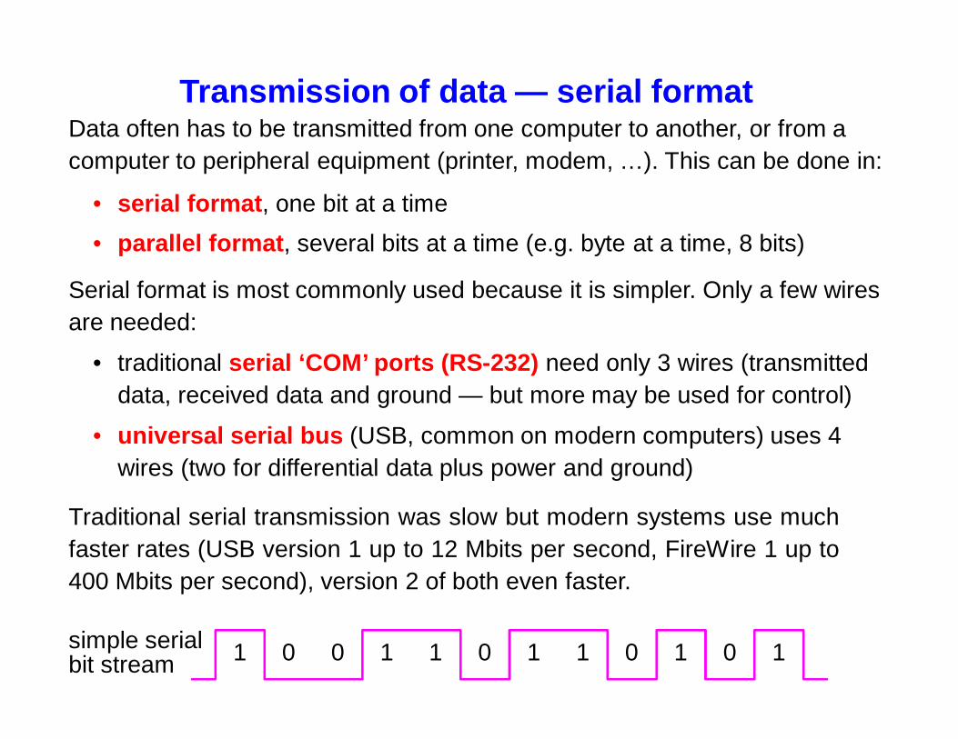
Transmission of data — serial formatData often has to be transmitted from one computer to another, or from a computer to peripheral equipment (printer, modem, …). This can be done in:
• serial format, one bit at a time• parallel format, several bits at a time (e.g. byte at a time, 8 bits)
Serial format is most commonly used because it is simpler. Only a few wires are needed:
• traditional serial ‘COM’ ports (RS-232) need only 3 wires (transmitted data, received data and ground — but more may be used for control)
• universal serial bus (USB, common on modern computers) uses 4 wires (two for differential data plus power and ground)
Traditional serial transmission was slow but modern systems use muchfaster rates (USB version 1 up to 12 Mbits per second, FireWire 1 up to400 Mbits per second), version 2 of both even faster.
1 0 0 1 1 0 1 1 0 1 0 1bit streamsimple serial

Parallel dataWhere higher speed is required, several bits (usually a small number of bytes, each of 8 bits) may be moved at once. More complicated connections are needed — more wires. Common applications include:
• inside the processor itself, e.g. our microcontroller handles bytes• inside a computer system on the bus (e.g. PCI) and interfaces to disk
drives (e.g. e.g. SCSI or IDE)— but these are now mainly serial
Interfaces have changed to serial because it is hard to ensure that all bits on a parallel bus arrive at the same time at the high speed of modern systems.

Parallel data
a UART (universal asynchronous receiver transmitter) or something similar.
Where higher speed is required, several bits (usually a small number of bytes, each of 8 bits) may be moved at once. More complicated connections are needed — more wires. Common applications include:
• inside the processor itself, e.g. our microcontroller handles bytes• inside a computer system on the bus (e.g. PCI) and interfaces to disk
drives (e.g. e.g. SCSI or IDE)— but these are now mainly serial
Interfaces have changed to serial because it is hard to ensure that all bits on a parallel bus arrive at the same time at the high speed of modern systems.
How do you interface a serial device to a computer?
How do we interface an external device that transmits serially with the bus of a computer that transfers one byte (8 bits) at a time?
• Use a shift register.In practice this would almost certainly be buried inside a larger circuit called

Use of shift register to serialize data
D Q D Q D Q D Q serial output
A B C D
Extra logic is added to the basic shift register so that all the flip-flops can be loaded in parallel (simultaneously), controlled by a shift/load input.
Once the data have been loaded, the clock is enabled and the values are shifted once per clock cycle. This causes the input data to be transferred to the output, one bit at a time — serial output (PISO).
The opposite process is used to read in serial data, fill up the shift register, and transfer it in parallel to a bus when the register is full (SIPO).
The register can also be parallel input – parallel output (PIPO).
Shift or rotate instructions can be used for the same process inside a microcontroller (if it doesn’t have a UART built in, which many do).
parallel data in
parallel load

237
• The data stored in ROM are always there, whether the power is on or not. A ROM can be removed from the PC, and then replaced, and the data it contains will still be there.
• Data stored in these chips is unchangeable, provides a measure of security against accidental or malicious changes to its contents. Unlike RAM, which can be changed as easily as it is read
– We will look at five of them to see how they differ in the way they are programmed, erased, and reprogrammed
ROM

238
Mask ROM• The mask ROM is usually referred to simply as a
ROM.
• A regular ROM is constructed from hard-wiredlogic, encoded in the silicon itself to perform a specificfunction that cannot be changed.
• They consume very little power and reliable but cannotreprogram or rewrite.
• Several types of user programmable ROMs have beendeveloped to overcome this disadvantage.

239
Programmable ROM (PROM)
• A mask ROM chip is very expensive and time-consuming tocreate in small quantities from scratch.
• Mainly, developers created a type of ROM known asprogrammable read-only memory (PROM).
• This is basically a blank ROM chip that can be written onlyonce using special equipment called a PROM programmer.
• PROM chips have a grid of columns and rows just as ordinaryROMs do.

240
• The difference is that every intersection of a column and rowin a PROM chip has a fuse connecting them.
• Since all the cells have a fuse, the initial (blank) state of aPROM chip is all 1s.
• The user cans selectively burn/blow any of these fuse links toproduce the desired stored memory data.
• A charge sent through a column will pass through the fuse in acell to a grounded row indicating a value of 1.
Programmable ROM (PROM)

241
• To change the value of a cell to 0, you use a PROM programmer to send a specific amount of current to the cell to break the connection between the column and row by burning out the fuse.
• This process is known as burning the PROM.
• Very few bipolar PROMs are still available today.
• TMS27PC256 is a very popular CMOS PROM with a capacity of 32K 8.
Programmable ROM (PROM)

242
Erasable Programmable ROM (EPROM)
• An EPROM is a ROM that can be erased andreprogrammed as often as desired. Once programmed.
• The EPROM is a non-volatile memory that will hold its storeddata indefinitely.
• A little glass window is provided in the top of the ROMpackage.
• Ultraviolet light of a specific frequency can be shined throughthis window for a specified period of time, which will erase allcells at the same time so that an erased EPROM stores all 1sand allow it to be reprogrammed again.

243
Erasable Programmable ROM (EPROM)
• EPROMs are configured using an EPROMprogrammer that provides voltage at specified levelsdepending on the type of EPROM used.
• Obviously this is much more useful than a regularPROM, but it does require the erasing light.
• EPROMs are available in a wide range of capacitiesand access times. The 27C64 is an example of 8K x 8CMOS EPROM

244
Electrically Erasable Programmable ROM (EEPROM)
• They require dedicated equipment and a labor-intensive process to remove and reinstall them eachtime a change is necessary.
• The next type of ROM is the EEPROM, which can beerased under software control.
• This is the most flexible type of ROM, and is nowcommonly used for holding BIOS programs

245
Electrically Erasable Programmable ROM (EEPROM)
• In EEPROMs the chip does not have to be removedto be rewritten, the entire chip need not be fullyerased to change a specific portion of it, andchanging the contents does not require additionaldedicated equipment.
• Instead of using UV light, you can return theelectrons in the cells of an EEPROM to normal withthe localized application of an electric field to eachcell.

246
Electrically Erasable Programmable ROM (EEPROM)
• This erases the targeted cells of the EEPROM, which can then be rewritten.
• EEPROMs are changed 1 byte at a time, which makes them versatile but slow.
• The Intel 2864 is an example of EEPROM with 8K 8 array with 13 address inputs and eight data I/O pins

247
Flash Memory
• Flash memories are so called because of their rapiderase and write times.
• EEPROM chips speed is too slow to use in manyproducts that required quick changes to the datastored on the chip.
• So a new type of EEPROM called Flash memory thatuses in-circuit wiring to erase by applying anelectrical field to the entire chip or to predeterminedsections of the chip called blocks.

248
Flash Memory
• Flash memory works much faster thantraditional EEPROMs because it writes data inchunks, usually 512 bytes in size, instead of 1byte at a time.
• The 28F256A CMOS IC is an example of flashmemory chip, which has a capacity of 32K 8.

The SRAM Memory Cell
• Circuit Schematic:– 4 NFETs and 2 PFETs: T1 & T2 called active devices; T3
& T4 called the I/O devices; T5 & T6 sometimes called loads.
– The cell is comprised of two cross-coupled inverters (positive feedback).
– 2 vertical lines (bit lines B0 & B1) are used for sensing state of cell and writing data in the cell
– 1 horizontal line (word line WL) is used to select a row of cells for writing or reading and to prevent the unselected rows of cells from being disturbed.
• Circuit Operation:– The cell has two stable states: “0” and “1”
• “0” State = Node X0 high and Node X1 low; T2 & T5 are ON, T1 & T6 are OFF.
• “1” State = Node X1 high and Node X0 low; T1 & T6 are ON; T2 & T5 are OFF.
• No dc current flows in either state. – Write: raise WL to Vdd; pull one bit line high & pull the
other bit line low– Read: raise WL to Vdd; precharge bit lines to ½ Vdd
Vdd
B1B0
WL
X0 X1
T5 T6
T2T1
T3T4

SRAM Memory Array Organization• READ Operation:
– Word Decode circuitry selects one of n word lines and drives high to Vdd (say WL2); other word lines held at gnd.
– Bit Lines all precharged to half Vdd– Selected cell’s I/O devices turned ON
and apply a V to bit line pair– Sense amp triggers on bit line V and
stores read data “0” or “1”• WRITE Operation:
– Selected WL is driven high to Vdd by word decode circuitry turning ON I/O devices in selected cells
– Selected bit column has one BL pulled high to Vdd and the other pulled low to gnd, thus writing the selected cell.
– Unselected bit columns merely perform a READ operation.
SRAMCell11
WordDecode
(RowDecode)
Sense Amplifiersand Off-Chip Drivers/Buffers
Bit Decode (Column Decode)and Write Drivers
SRAMCell12
SRAMCell13
SRAMCell21
SRAMCell22
SRAMCell23
SRAMCell31
SRAMCell32
SRAMCell33
Data Out
WordAddr
BitAddr
Data In
251
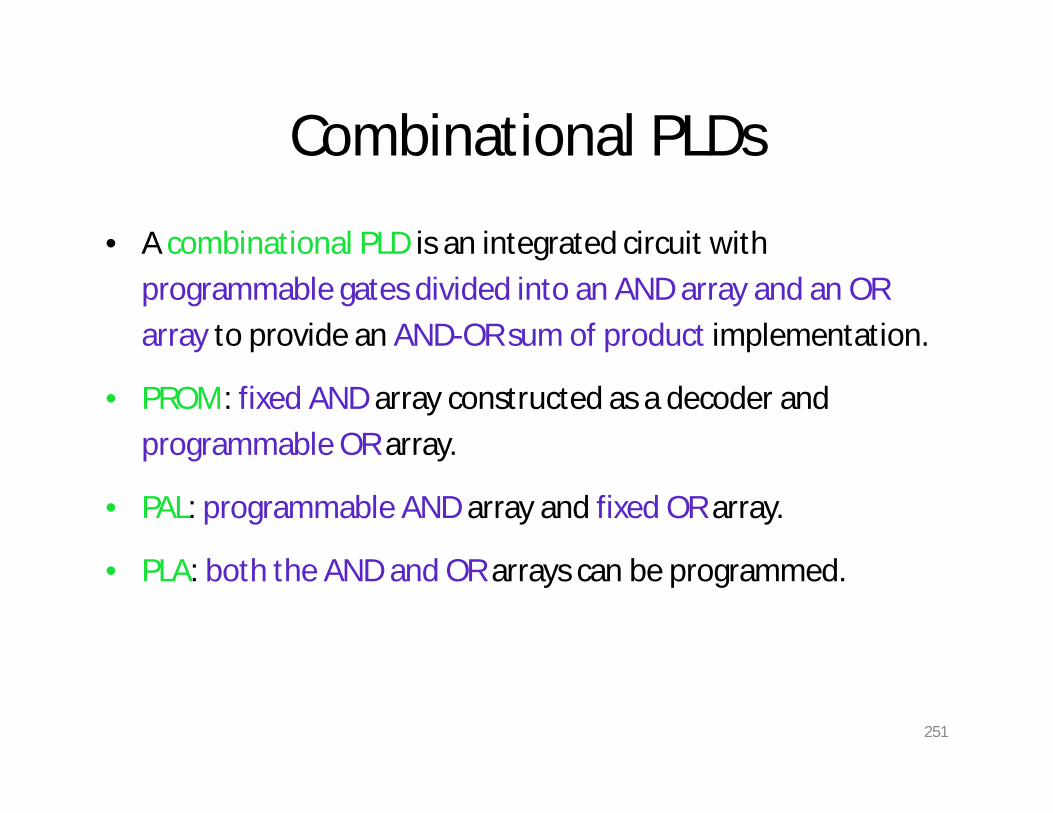
Combinational PLDs
• A combinational PLD is an integrated circuit with programmable gates divided into an AND array and an OR array to provide an AND-OR sum of product implementation.
• PROM: fixed AND array constructed as a decoder and programmable OR array.
• PAL: programmable AND array and fixed OR array.
• PLA: both the AND and OR arrays can be programmed.

252
Combinational PLDs
253
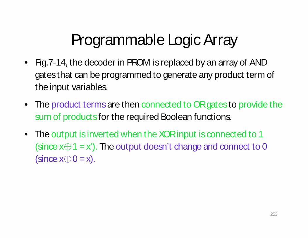
Programmable Logic Array• Fig.7-14, the decoder in PROM is replaced by an array of AND
gates that can be programmed to generate any product term of the input variables.
• The product terms are then connected to OR gates to provide the sum of products for the required Boolean functions.
• The output is inverted when the XOR input is connected to 1 (since x⊕1 = x’). The output doesn’t change and connect to 0 (since x⊕0 = x).

254
PLA
F1 = AB’+AC+A’BC’F2 = (AC+BC)’
255
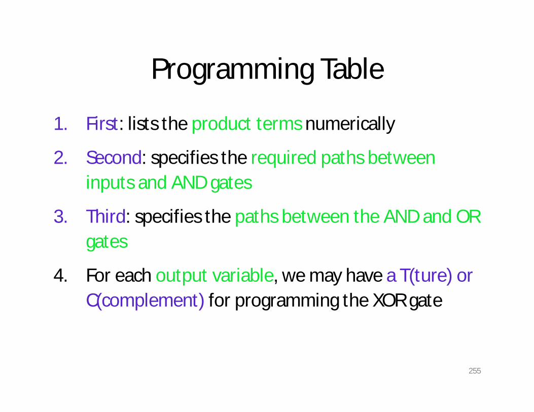
Programming Table
1. First: lists the product terms numerically
2. Second: specifies the required paths between inputs and AND gates
3. Third: specifies the paths between the AND and OR gates
4. For each output variable, we may have a T(ture) or C(complement) for programming the XOR gate

256
Simplification of PLA
• Careful investigation must be undertaken in order to reduce the number of distinct product terms, PLA has a finite number of AND gates.
• Both the true and complement of each functionshould be simplified to see which one can be expressed with fewer product terms and which one provides product terms that are common to other functions.
257
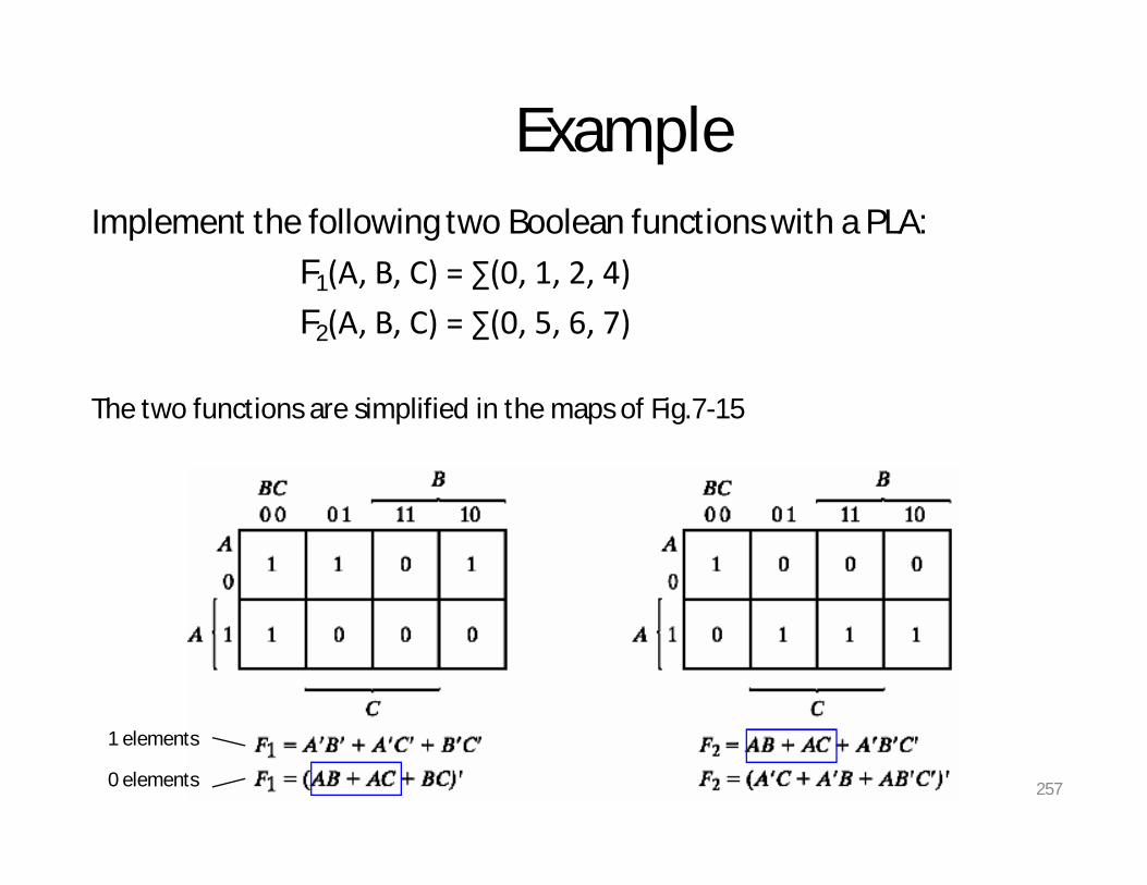
ExampleImplement the following two Boolean functions with a PLA:
F1(A, B, C) = ∑(0, 1, 2, 4)F2(A, B, C) = ∑(0, 5, 6, 7)
The two functions are simplified in the maps of Fig.7-15
1 elements
0 elements

258
PLA table by simplifying the function
• Both the true and complement of the functions are simplified in sum of products.
• We can find the same terms from the group terms of the functions of F1, F1’,F2 and F2’ which will make the minimum terms.
F1 = (AB + AC + BC)’F2 = AB + AC + A’B’C’

259
PLA implementation
AB
AC
BC
A’B’C’

260
Programmable Array Logic• The PAL is a programmable logic device with a fixed OR array and a
programmable AND array.
261
PAL
• When designing with a PAL, the Boolean functions must be simplified to fit into each section.
• Unlike the PLA, a product term cannot be shared among two or more OR gates. Therefore, each function can be simplified by itself without regard to common product terms.
• The output terminals are sometimes driven by three-state buffers or inverters.

262
Examplew(A, B, C, D) = ∑(2, 12, 13)x(A, B, C, D) = ∑(7, 8, 9, 10, 11, 12, 13, 14, 15)y(A, B, C, D) = ∑(0, 2, 3, 4, 5, 6, 7, 8, 10, 11, 15)z(A, B, C, D) = ∑(1, 2, 8, 12, 13)
Simplifying the four functions as following Boolean functions:
w = ABC’ + A’B’CD’x = A + BCDw = A’B + CD + B’D’w = ABC’ + A’B’CD’ + AC’D’ + A’B’C’D = w + AC’D’ + A’B’C’D

263
PAL Table• z has four product terms, and we can replace by w with two
product terms, this will reduce the number of terms for z from four to three.

264
PAL implementation
A
B
C
D
w
x
y
z

265
Fuse map for example

266
Sequential Programmable Devices
• Sequential programmable devices include both gates and flip-flops.
• There are several types of sequential programmable devices, but the internal logic of these devices is too complex to be shown here.
• We will describe three major types without going into their detailed construction.

267
Sequential Programmable Devices
1. Sequential (or simple) Programmable Logic Device (SPLD)
2. Complex Programmable Logic Device (CPLD)
3. Field Programmable Gate Array (FPGA)

268
FPLS
• The first programmable device developed to support sequential circuit implementation is the field-programmable logic sequencer(FPLS).
• A typical FPLS is organized around a PLA with several outputs driving flip-flops.
• The flip-flops are flexible in that they can be programmed to operate as either JK or D type.
• The FPLS did not succeed commercially because it has too many programmable connections.

269
SPLD
• Each section of an SPLD is called a macrocell.
• A macrocell is a circuit that contains a sum-of-products combinational logic function and an optional flip-flop.
• We will assume an AND-OR sum of products but in practice, it can be any one of the two-level implementation presented in Sec.3-7.

270
Macrocell• Fig.7-19 shows the logic of a basic macrocell.• The AND-OR array is the same as in the combinational PAL shown
in Fig.7-16.

271
CPLD• A typical SPLD has from 8 to 10 macrocells within one IC package.
All the flip-flops are connected to the common CLK input and all three-state buffers are controlled by the EO input.
• The design of a digital system using PLD often requires the connection of several devices to produce the complete specification. For this type of application, it is more economical to use a complex programmable logic device (CPLD).
• A CPLD is a collection of individual PLDs on a single integrated circuit.
272
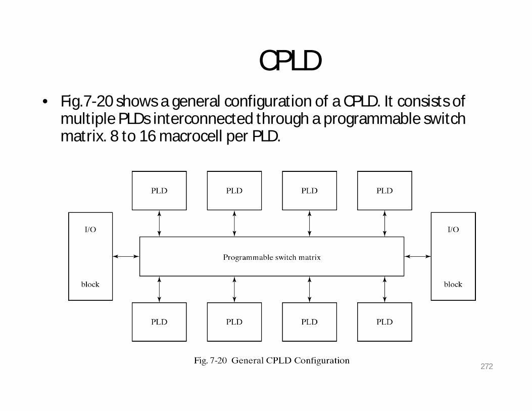
CPLD• Fig.7-20 shows a general configuration of a CPLD. It consists of
multiple PLDs interconnected through a programmable switch matrix. 8 to 16 macrocell per PLD.

273
Gate Array
• The basic component used in VLSI design is the gate array.
• A gate array consists of a pattern of gates fabricated in an area of silicon that is repeated thousands of times until the entire chip is covered with the gates.
• Arrays of one thousand to hundred thousand gates are fabricated within a single IC chip depending on the technology used.

274
FPGA
• FPGA is a VLSI circuit that can be programmed in the user’s location.
• A typical FPGA logic block consists of look-up tables, multiplexers, gates, and flip-flops.
• Look-up table is a truth table stored in a SRAM and provides the combinational circuit functions for the logic block.

275
Differential of RAM and ROM in FPGA
• The advantage of using RAM instead of ROM to store the truth table is that the table can be programmed by writing into memory.
• The disadvantage is that the memory is volatile and presents the need for the look-up table content to be reloaded in the event that power is disrupted.

Algorithmic State Machines

Introduction
Digital system is specified by the following three components:
• The set of registers in the system• The operations that are performed on the
data stored in the registers.• The control that supervises the sequences
of operations in the system.

Control and Datapath Interaction

Datapath
• Binary information in digital systems classified as either data or control.
• Data – bits of information manipulated by performing arithmetic and logic operations.
• Hardware components realizing above operations are adders, decoders, multiplexers, counters e.t.c

Control Path
• Command signals used to supervise execution of algorithms by datapath.
• Bi-directional communication with datapath through status conditions used to determine the sequence of control signals.
• Control logic inherently sequential.
• Control logic is usually implemented using FSMs
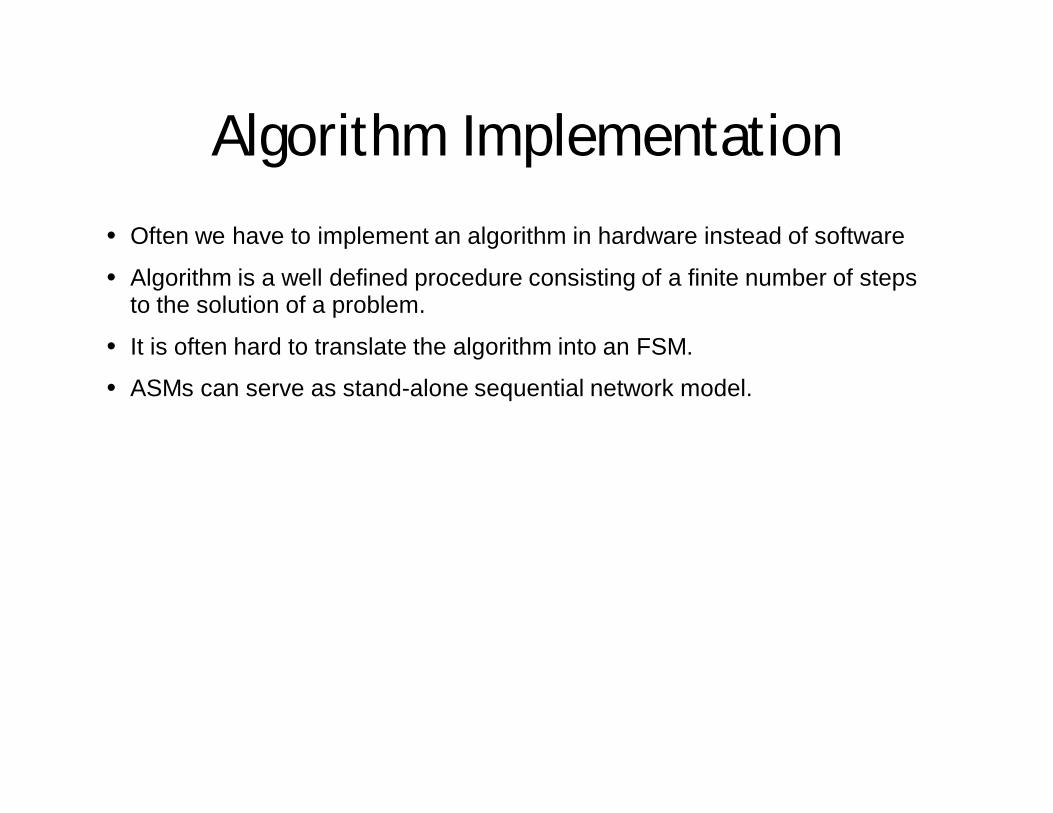
• Often we have to implement an algorithm in hardware instead of software
• Algorithm is a well defined procedure consisting of a finite number of steps to the solution of a problem.
• It is often hard to translate the algorithm into an FSM.
• ASMs can serve as stand-alone sequential network model.
Algorithm Implementation

Algorithmic State Machine•Used to graphically describe the operations of an FSM more concisely
•Resembles conventional flowcharts – differs in
interpretation.
•Conventional flowchart – sequential way of
representing procedural steps and decision paths
for algorithm
-No time relations incorporated
•ASM chart – representation of sequence of
events together with timing relations between
states of sequential controller and events
occurring while moving between steps

ASM Chart•Three basic elements: state box, decision
box and conditional box
-State and decision boxes used in conventional
flowcharts
-Conditional box characteristic to ASM
•State box
-Used to indicate states in control sequence
•Register operations and output signals used to
control generation of next state written

State box•Represents one state in the ASM.
•May have an optional state output list.
•Single entry.
•Single exit to state or decision boxes.

State Box
State name T3
•Binary code of T3 – 011
•Register operation R <- 0
•START – name of
outputs signal generated
in this stage

Decision box
• Provides for next alternatives and conditional outputs.
• Conditional output based on logic value of Boolean expression involving external input variables and status information.
• Single entry.• Dual exit, denoting if Boolean
expression is true or false.• Exits to decision, state or conditional
boxes.

Decision Box•Input condition subject to
test inside diamond shape
box
•Two or more outputs
represent exit paths
dependant on value of
condition in decision box
•Two paths for binary basedconditions

Conditional output box
• Provides a listing of output variables that are to have a value logic-1, i.e., those output variables being asserted.
• Single entry from decision box.• Single exit to decision or state box.

•In state T1
Output signal START
generated
Status of input E
checked
•If E = 1, R <- 0,
otherwise remains
unchanged
•Conditional
operation executed
depending on result
of coming from
decision box
Conditional Box

ASM Block
• Consists of the interconnection of a single state box along with one or more decision and/or conditional boxes.
• It has one entry path which leads directly to its state box, and one or more exit paths.
• Each exit path must lead directly to a state, including the state box in itself.
• A path through an ASM block from its state box to an exit path is called a link path.

Timing Considerations All sequential elements in datapath and control
path controlled by master-clock generator.
Does not necessarily imply single clock in design.
•Multiple clocks can be obtained through division of clock
signals from master-clock generator.
•Not only internal signals, but also inputs
synchronized with clock.
•Normally, inputs supplied by other devices working
with the same master clock.
•Some inputs can arrive asynchronously
Difficult to handle by synchronous designs, require
asynchronous glue-logic.

•In conventional flowchart, evaluation of each chart element takes one clock cycle
Step 1: Reg A incremented
Step 2: Condition E evaluated
Step 3: Based on evaluation results, state
T2, T3 or T4 entered
•In ASM the entire block considered
as one unit
•All operations within block occurring
during single edge transition
The next state evaluated during the same clock
System enters next state T2, T3 or T4 during transition of next clock
ASM Block

ASM Block
• An ASM block describes the operation of the system during the state time in which it is in the state associated with the block.
• The outputs listed in the state box are asserted.• The conditions indicated in the decision boxes are evaluated
simultaneously to determine which link path is to be followed.• If a conditional box is found in the selected path then the outputs
found in its output list are asserted.• Boolean expression may be written for each link path. The selected
link paths are those that evaluate to logic-1.

Analyze a sequential circuit using JK Flip-Flops

Analysis (JK FF)The flip-flop input equations are:
The sequential circuit output equation is:
The next-state equations for the flip-flops are:

The corresponding next-state (K-) maps are
The state table, and transition table, is then:
The state diagram can then be drawn from the state table:
MODE OF OPERATIONS Steady-state condition: Current states and next states are the same Difference between Y and y will cause a transition
Fundamental mode: •No simultaneous changes of two or more variables• The time between two input changes must be longer than the time it takes the circuit to a stable state •The input signals change one at a time and only when the circuit is in a stable condition Fundamental Mode
Pulse Mode: the inputs and outputs are represented by pulsesonly one input is allowed to have pulse present at any time Similar to synchronous sequential circuits except without a clock signal