Embed Size (px)
Citation preview

VIRTUAL NANOLAB BY QUANTUMWISE
Presentation by:
Kwesi Eshun
Supervisor: Dr. Qiliang Li

ORDER OF PRESENTATION
1. Introduction
2. Structures
3. Models for Simulation and Analysis
4. Perspective: Si/2D Structures (MoS2 or WSe2)
5. P-N Junctions
6. Effective Mass
7. Transistors
8. Uses
9. Conclusion
INTRODUCTION
• A simulation software for nanoscience.
• An Ideal tool for teaching basic concepts of nanotechnology, solid
state physics etc.
• Used by over 150 research groups at leading universities,
government labs in a wide range of application areas.
• More than 600 scientific articles have been published using ATK
(Atomistix ToolKit).
• Has a GUI that can be used for other atomic-scale simulations as
well.
• Runs on a python scripting interface.
• Can be used to calculate and analyze the electronic properties and
structure of nanowires, semiconductors and pn junctions.

Structures
• Molecules eg. Benzene
• Crystals eg Silver(fcc), Si(fcc) etc.
• Fullerenes – carbon nanotubes
Benzene
Ag<111>
Fullerene
MODELS AND ANALYSIS FOR SIMULATION
• Version 12.8.2
New models included that are not found in older versions such
as the Tight-Binding model and Socorro model.
Models used for simulation in current version (13.8 release
candidate) include:
1. DFT-LDA,GGA,MGGA
2. SE- Extended Huckel model
3. SE- Slater Koster model
4. Classical
5. Abinit
New features introduced in the current version are phonon
calculations, Shell-wise Hubbard + U model and many more.

ANALYSIS
Types of analysis:1. Bandstructure
2. IV curve
3. Transmission Spectrum/Pathways
4. Electron Difference Density/Electrostatic Difference Potential
5. Density of States
6. Electron Density
7. Forces
8. Stress
9. Mulliken Population

How-to-Use
1. Create structure using the Builder function.
2. Define lattice parameters or modify structure to suite the simulation using the tools in the Builder
interface. Then send the final structure to the Script Generator for analysis and calculation.
3. In the Script Generator, define model to be used for simulation and and select type of analysis to run. The
Editor tool can be used to manually configure simulation settings.
4. From the Script Generator, send structure to the Job Manager then run simulation.
5. After simulation, results can be analyzed using the Analyzer tool and the 3D structure can also be viewed
with the Viewer tool.
Main VNL window

Steps
1. Builder Menu

Script Generator
2. Script Generator
Calculator to define
model for simulation

Job Manager
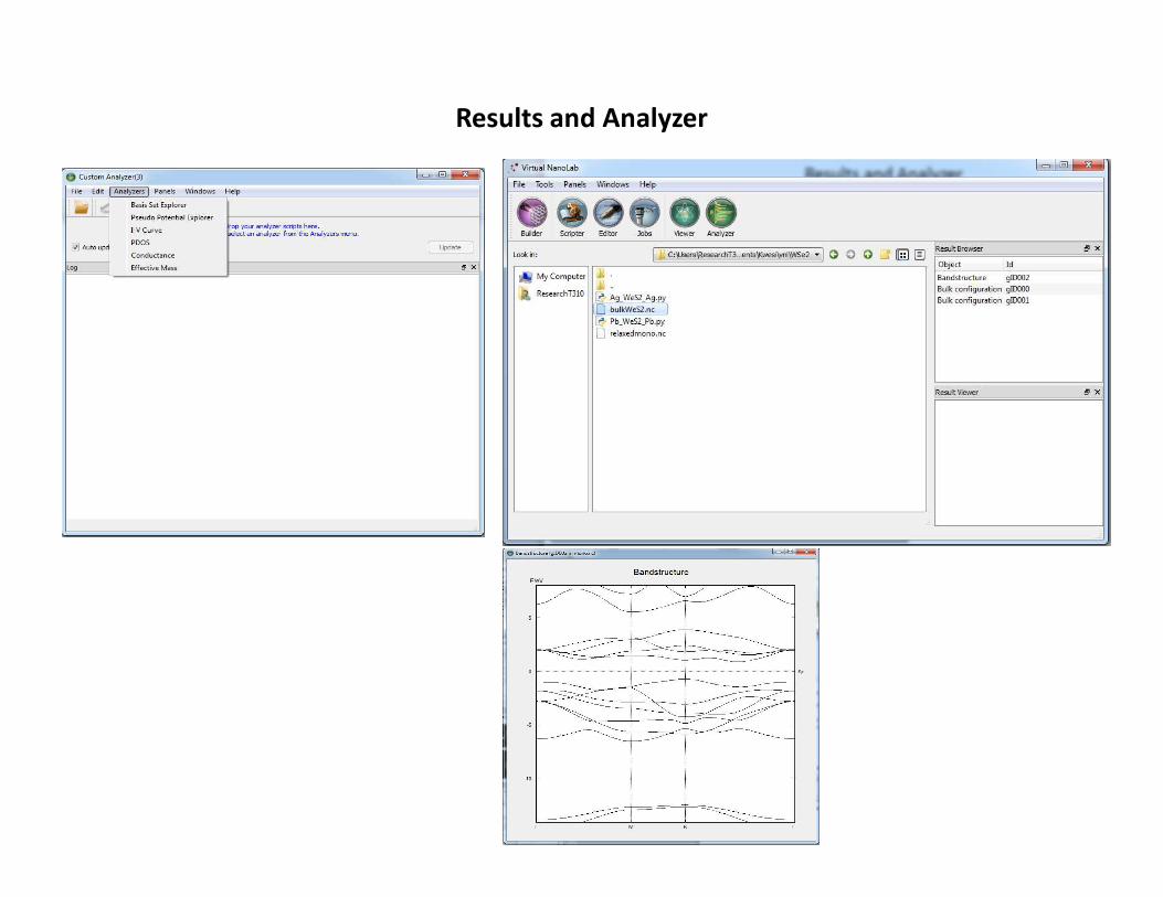
Results and Analyzer

PERSPECTIVE: Si/2D structures
Si: Has a band gap of 1.1eV
www.users-phys.au-dk
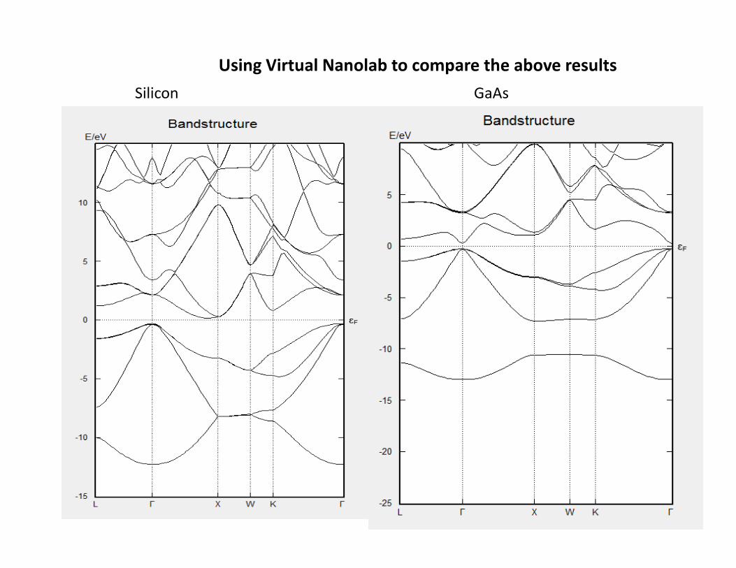
Silicon GaAs
Using Virtual Nanolab to compare the above results

2D Structures-MoS2
Hexagonal Structure
Nanosheet
MoS2
Nanotube

Monolayer and Double layer MoS2
with VNL
1.8eV
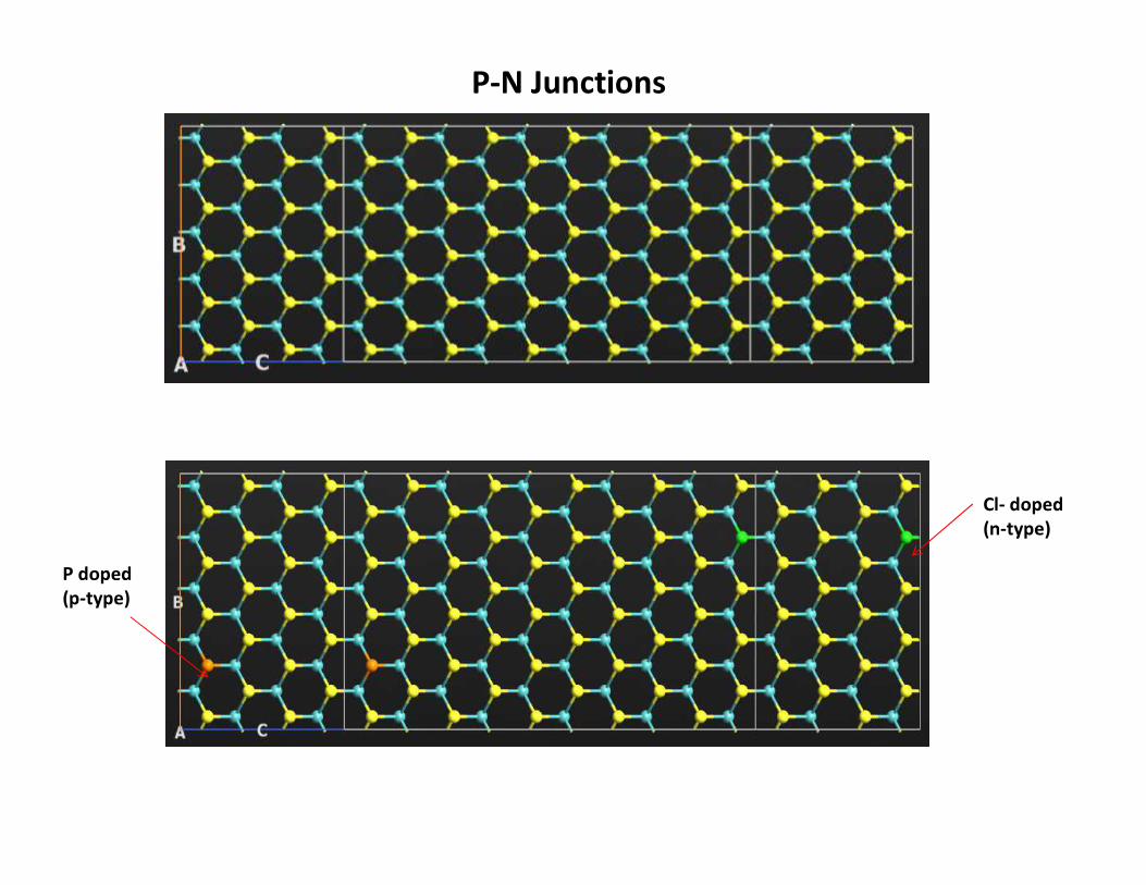
P-N Junctions
P doped
(p-type)
Cl- doped
(n-type)

Diode behavior
(Appl. Phys. Lett. 102, 093104 (2013); doi: 10.1063/1.4794802)
FIG. 1. Calculated current-voltage characteristics at
300K of the constructed p-n junction.
FIG. 2. The electronic structures of Cl-doped (a) and
P-doped (b) MoS2 supercell, compared with undoped
band structures (aligned with doped ones); the
wavefunctions of the lowest conduction band of Cl-doped
(c) and the highest valence band of P-doped (d) at K
point of the Brillouin zone. The arrows indicate the
position of impurity atoms.

Si (111) and Si (100)
<111>
<100>
Bandstructure simulation
of different directions of
Si can be done

Effective Mass
Fig. 1 Effective mass for
Si<111>
Fig. 2 Effective mass for
Si<100>

Si(100) FET
www.quantumwise.com
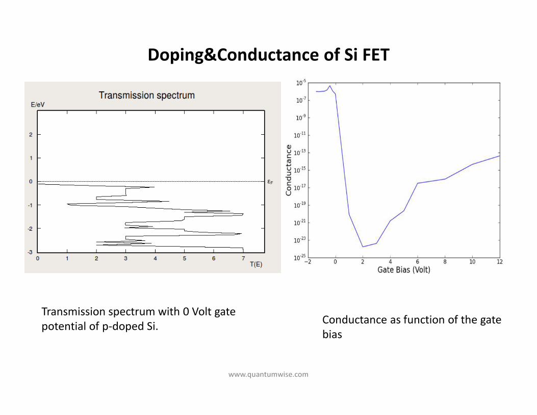
Doping&Conductance of Si FET
Transmission spectrum with 0 Volt gate
potential of p-doped Si.Conductance as function of the gate
bias
www.quantumwise.com

Uses of VNL
There is a wide range of usage for Virtual Nanolab, including:
1. Graphene
2. Nanowires
3. Magnetic Tunnel Junctions
4. Molecular Electronics
5. Three-Terminal Devices
6. Single-Electron Transistors

Conclusion
1. Most electronic properties of nanostructures can be simulated with
Virtual Nanolab.
2. Provides a vivid understanding of the band properties of semiconductors,
pn junctions.
3. An Ideal tool for teaching basic concepts of nanotechnology, solid state
and device physics.
4. Tutorials can be found on www.quantumwise.com/tutorials


![ffisfr.r{Knbr.gov.bd/uploads/transfer-posting/IMG_20190325_0007_compressed.pdfrr€q]qfr qli.,rrffi ']{rq-f,](https://img.pdfslide.us/doc/110x75/5f9636c2d478b3751f26929d/ffisfrrknbrgovbduploadstransfer-postingimg201903250007-rraqqfr-qlirrffi.jpg)