Embed Size (px)
Citation preview

VSOP584..www.vishay.com Vishay Semiconductors
Not for New Designs
Rev. 1.9, 04-Apr-18 1 Document Number: 82444
THIS DOCUMENT IS SUBJECT TO CHANGE WITHOUT NOTICE. THE PRODUCTS DESCRIBED HEREIN AND THIS DOCUMENTARE SUBJECT TO SPECIFIC DISCLAIMERS, SET FORTH AT www.vishay.com/doc?91000
Preamplifier Circuit for IR Remote Control
DESIGN SUPPORT TOOLS
FEATURES• Narrow bandpassfilter for all common carrier
frequencies
• High immunity against DC light
• Intelligent AGC to suppress disturbance from fluorescent lamps and CRTs
• Low power consumption
• Wide supply voltage range
• High immunity against ripple on the supply voltage
• Output active low
• IC manufactured in CMOS technology
• Small QFN package with 2 mm width
• Material categorization: for definitions of compliance please see www.vishay.com/doc?99912
DESCRIPTIONThe VSOP584.. is designed for use in an IR receiver application together with a photo pin diode. It is a sophisticated receiver concept that is very sensitive to data signals and compatible with the most common data formats for IR remote control. On the other hand it is immune to DC current caused by DC light sources such as tungsten bulbs. The disturbance signal of fluorescent lamps is suppressed; there are no unwanted pulses at the output.
BLOCK DIAGRAM (Simplified) APPLICATION CIRCUIT
Vishay recommends using a photodiode with at least 2.3 mm2 area. The connection between the photodiode and pin 7 should be kept as short as possible and carefully shielded to prevent noise coupling.
22906
click logo to get started
AvailableModels
PARTS TABLEAGC RECOMMENDED FOR LONG BURST CODES (AGC4)
Carrier frequency
36 kHz VSOP58436 (1)(2)(3)
38 kHz VSOP58438 (4)(5)(6)
Package VSOP
Pinning 1, 4, 5 = N.C., 2 = VS, 3 = OUT, 6, 8 = GND, 7 = IN
Dimensions (mm) 2.0 W x 2.0 H x 0.76 D
Mounting SMD
Application Remote control
Best remote control code (1) RC-5 (2) RC-6 (3) Panasonic (4) NEC (5) Sharp (6) r-map
+ VS
Output,to μC
GND
Input, from photodiode
Bias Controlled gain amplifier
Automatic gain control
Band-pass-filter
33 kΩAutomatic threshold control
Inte-grator
21536-2
21537-5
The RC filter is optional to improve the EOS robustnessand the immunity to supply voltage ripple. We recommendto keep the distance between the photodiode and the inputof the VSOP584.. as short as possible.
Microcontrolleror other logicto decode theIR signal
100 Ω
0.22 μF
VS = 2.7 V to 5.5 V
0 V
VSOP584..VS
GND
IN OUT

VSOP584..www.vishay.com Vishay Semiconductors
Not for New Designs
Rev. 1.9, 04-Apr-18 2 Document Number: 82444
THIS DOCUMENT IS SUBJECT TO CHANGE WITHOUT NOTICE. THE PRODUCTS DESCRIBED HEREIN AND THIS DOCUMENTARE SUBJECT TO SPECIFIC DISCLAIMERS, SET FORTH AT www.vishay.com/doc?91000
Note• Stresses beyond those listed under “Absolute Maximum Ratings” may cause permanent damage to the device. This is a stress rating only
and functional operation of the device at these or any other conditions beyond those indicated in the operational sections of this specification is not implied. Exposure to absolute maximum rating conditions for extended periods may affect the device reliability.
Fig. 1 - Testsignal
ABSOLUTE MAXIMUM RATINGS (Tamb = 25 °C, unless otherwise specified)PARAMETER TEST CONDITION SYMBOL VALUE UNIT
Supply voltage Pin 2 VS -0.3 to +6 V
Supply current Pin 2 IS 5 mA
Output voltage Pin 3 VO -0.3 to (VS + 0.3) V
Output sink current Pin 3 IO 5 mA
Power dissipation Tamb ≤ 85 °C Ptot 10 mW
Operating temperature range Tamb -25 to +85 °C
Storage temperature range Tstg -25 to +85 °C
ESD stress, HBMPin 2, pin 3, MIL-STD-883C VESD 2000 V
Pin 7, MIL-STD-883C VESD 500 V
ESD stress, MMPin 2, pin 3, MIL-STD-883C VESD 200 V
Pin 7, MIL-STD-883C VESD 100 V
ELECTRICAL CHARACTERISTICS (Tamb = -30 °C to +85 °C)PARAMETER TEST CONDITION SYMBOL MIN. TYP. MAX. UNIT
Supply voltage VS 2.7 - 5.5 V
Supply current (pin 2) IIN = 0, VS = 5 V IS 0.65 0.85 1.05 mA
Output voltage low (pin 3) IOL = 2 mA VOL - - 100 mV
Output voltage high (pin 3) IOL = 0 VOH VS - 0.25 - - V
Internal pull up resistor (pin 2, pin 3) RPU - 33 - kΩ
Max. input DC current VIN > 0 IIN-DCmax. 400 - - μA
Min. signal detection current IIN-DC = 0, fC = fBPF IIN-min. - 700 1000 pA
IIN-DC = 100 μA, fC = fBPF IIN-min. - 5 10 nA
Output pulse widthIIN-DC = 0, fC = fBPF,
IIN = 0.8 nA to 50 μA,testsignal see fig. 1, BER ≤ 2%
tpo tpi - 6/f0 tpi tpi + 6/f0 μs
Accuracy of bandpass center frequency Tamb = + 25 °C fBPF f0 - 4 % f0 f0 + 4 % kHz
Bandwidth of bandpassfilter -3 dB, f0 = 38 kHz B - 3.8 - kHz
burst length tpI
output pulse width tpo
IIN
VOUT
one carrier cycle 1/fC
burst length of input signal tpi
output pulse width tpo
IIN
VOUT21538

VSOP584..www.vishay.com Vishay Semiconductors
Not for New Designs
Rev. 1.9, 04-Apr-18 3 Document Number: 82444
THIS DOCUMENT IS SUBJECT TO CHANGE WITHOUT NOTICE. THE PRODUCTS DESCRIBED HEREIN AND THIS DOCUMENTARE SUBJECT TO SPECIFIC DISCLAIMERS, SET FORTH AT www.vishay.com/doc?91000
TYPICAL CHARACTERISTICS (Tamb = 25 °C, VS = 3.3 V, unless otherwise specified)
Fig. 2 - Output Pulse Diagram
Fig. 3 - Sensitivity vs. DC Input Current
Fig. 4 - Bandpassfilter Characteristic
Fig. 5 - Suppression of Ripple on Supply Voltage
Fig. 6 - Sensitivity vs. Temperature
Fig. 7 - Maximum Envelope Duty Cycle
0
0.1
0.2
0.3
0.4
0.5
0.6
0.7
0.8
0.9
1.0
0.1 10 1000 100 000
TOFF
tpo
Testsignal: tpi = 0.6 ms
burst repetition time = 1.2 ms
21539
Out
put P
ulse
Wid
th (
ms)
IIN - Input Current (nA)
I IN-m
in. -
Min
imum
Det
ectio
n C
urre
nt (
nA)
DC Input Current (µA)
0
0.5
1.0
1.5
2.0
2.5
3.0
3.5
4.0
4.5
5.0
0.01 0.1 1 10 100
Wavelength of ambientillumination: λ = 950 nm
Frequency (kHz)
I IN-m
in. -
Min
imum
Det
ectio
n C
urre
nt (
nA)
0
0.5
1.0
1.5
2.0
2.5
32 34 36 38 40 42 44
VSOP58438
1 10 100 1000
I IN-m
in. -
Min
imum
Det
ectio
n C
urre
nt (
nA)
ΔVS - AC Ripple on DC Supply Voltage (mVPP)
0
0.5
1.0
1.5
2.0
2.5
3.0
3.5
4.0
4.5
5.0
f = 100 Hz
f = 10 kHz
f = f0
- 30 - 10 10 30 50 70 90
I IN-m
in. -
Min
imum
Det
ectio
n C
urre
nt (
nA)
Tamb - Ambient Temperature (°C)
0.3
0.4
0.5
0.6
0.7
0.8
0.9
1.0
Max
imum
Env
elop
e D
uty
Cyc
le
Burstlength (Number of Cycles/Burst)
0
0.1
0.2
0.3
0.4
0.5
0.6
0.7
0.8
0 50 100 150
IIN = 5 nA

VSOP584..www.vishay.com Vishay Semiconductors
Not for New Designs
Rev. 1.9, 04-Apr-18 4 Document Number: 82444
THIS DOCUMENT IS SUBJECT TO CHANGE WITHOUT NOTICE. THE PRODUCTS DESCRIBED HEREIN AND THIS DOCUMENTARE SUBJECT TO SPECIFIC DISCLAIMERS, SET FORTH AT www.vishay.com/doc?91000
PACKAGE DIMENSIONS in millimeters
Proposed hole layoutfrom component side(for reference only)
technical drawingsaccording to DINspecifications
Not indicated tolerances ± 0.1
Drawing-No.: 6.550-5314.03-4Issue: 1; 07.12.15
0.76
± 0
.05
0.2
ref.
2
2
0.5 typ. (6 x)
(8 x)0.25 ± 0.05(8
x)
0.3
± 0
.1
0.2
min
.
0.9
± 0
.15
1.6 ± 0.15
0.25
x 4
5°
10:1
0.35 (8 x)(8 x
)0.
65
1.3
0.5 (6 x)
1. Coplanarity (0.1 mm) applies to the exposed pad as well as the exposed terminals.2. Package dimension does not include mold flash, protrusions, burrs or metal smearing.
1Pinning:
1. n.c.
2. VS
3. Out
4. n.c.
5. n.c.
6. GND
7. IN
8. GND
5438YWW
For example 38 kHz
Marking area
PIN 1 indicator
Chamfered cornerPIN 1 indicator
Exposed pad
0.1
4
8 5

VSOP584..www.vishay.com Vishay Semiconductors
Not for New Designs
Rev. 1.9, 04-Apr-18 5 Document Number: 82444
THIS DOCUMENT IS SUBJECT TO CHANGE WITHOUT NOTICE. THE PRODUCTS DESCRIBED HEREIN AND THIS DOCUMENTARE SUBJECT TO SPECIFIC DISCLAIMERS, SET FORTH AT www.vishay.com/doc?91000
ASSEMBLY INSTRUCTIONSReflow Soldering
• Set the furnace temperatures for pre-heating and heating in accordance with the reflow temperature profile as shown in the diagram. Exercise extreme care to keep the maximum temperature below 260 °C. The temperature shown in the profile means the temperature at the device surface. Since there is a temperature difference between the component and the circuit board, it should be verified that the temperature of the device is accurately being measured
• Handling after reflow should be done only after the work surface has been cooled off
Manual Soldering
• Use a soldering iron of 25 W or less. Adjust the temperature of the soldering iron below 300 °C
• Finish soldering within 3 s
• Handle products only after the temperature has cooled off.
VISHAY LEAD (PB)-FREE REFLOW SOLDER PROFILE
max. 120 s max. 100 s
max. 20 s
Max. ramp up 3 °C/s
max. 260 °C
10
100
1000
10000
0
50
100
250
300
0 300
Axis Title
2nd
line
Tem
pera
ture
(°C
)
Time (s)25020015010050
200
150
245 °C
217 °C240 °C255 °C
Max. ramp down 6 °C/s
Max. 2 cycles allowed
19800

VSOP584..www.vishay.com Vishay Semiconductors
Not for New Designs
Rev. 1.9, 04-Apr-18 6 Document Number: 82444
THIS DOCUMENT IS SUBJECT TO CHANGE WITHOUT NOTICE. THE PRODUCTS DESCRIBED HEREIN AND THIS DOCUMENTARE SUBJECT TO SPECIFIC DISCLAIMERS, SET FORTH AT www.vishay.com/doc?91000
TAPING VERSION VSOP DIMENSIONS in millimeters

VSOP584..www.vishay.com Vishay Semiconductors
Not for New Designs
Rev. 1.9, 04-Apr-18 7 Document Number: 82444
THIS DOCUMENT IS SUBJECT TO CHANGE WITHOUT NOTICE. THE PRODUCTS DESCRIBED HEREIN AND THIS DOCUMENTARE SUBJECT TO SPECIFIC DISCLAIMERS, SET FORTH AT www.vishay.com/doc?91000
REEL DIMENSIONS in millimeters
LABELStandard bar code labels for finished goods
The standard bar code labels are product labels and used for identification of goods. The finished goods are packed in final packing area. The standard packing units are labeled
with standard bar code labels before transported as finished goods to warehouses. The labels are on each packing unit and contain Vishay Semiconductor GmbH specific data.
REEL
REEL SIZE (inch) REEL WIDTH (mm) TRAILER LENGTH (mm) LEADER LENGTH (mm) QANTITY PER REEL
7 8.4 160 400 3000
22610
ReelSize
Reel Width
VISHAY SEMICONDUCTOR GMBH STANDARD BAR CODE PRODUCT LABEL (finished goods)PLAIN WRITTING ABBREVIATION LENGTH
Item-description - 18
Item-number INO 8
Selection-code SEL 3
LOT-/serial-number BATCH 10
Data-code COD 3 (YWW)
Plant-code PTC 2
Quantity QTY 8
Accepted by ACC -
Packed by PCK -
Mixed code indicator MIXED CODE -
Origin xxxxxxx+ Company logo
LONG BAR CODE TOP TYPE LENGTH
Item-number N 8
Plant-code N 2
Sequence-number X 3
Quantity N 8
Total length - 21
SHORT BAR CODE BOTTOM TYPE LENGTH
Selection-code X 3
Data-code N 3
Batch-number X 10
Filter - 1
Total length - 17
VSOP584..www.vishay.com Vishay Semiconductors
Not for New Designs
Rev. 1.9, 04-Apr-18 8 Document Number: 82444
THIS DOCUMENT IS SUBJECT TO CHANGE WITHOUT NOTICE. THE PRODUCTS DESCRIBED HEREIN AND THIS DOCUMENTARE SUBJECT TO SPECIFIC DISCLAIMERS, SET FORTH AT www.vishay.com/doc?91000
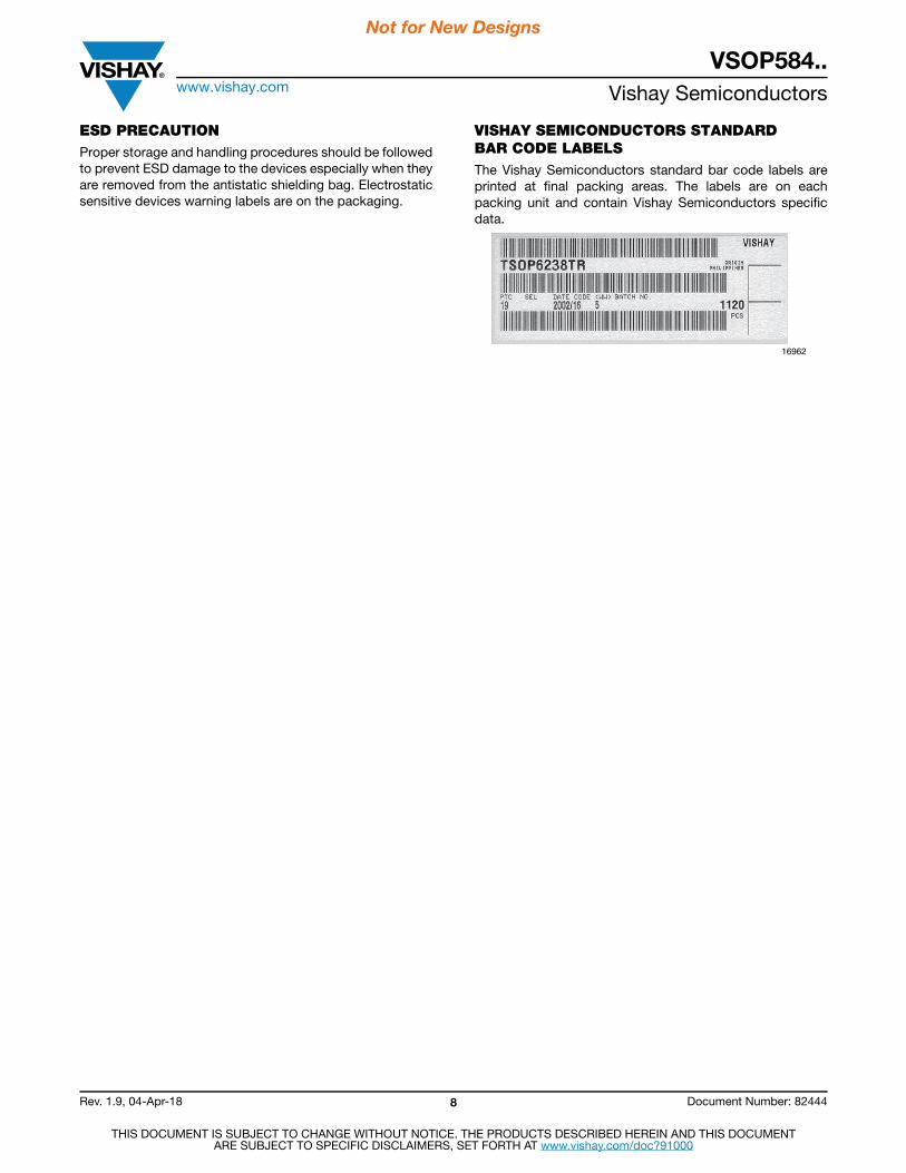
ESD PRECAUTIONProper storage and handling procedures should be followed to prevent ESD damage to the devices especially when they are removed from the antistatic shielding bag. Electrostatic sensitive devices warning labels are on the packaging.
VISHAY SEMICONDUCTORS STANDARD BAR CODE LABELSThe Vishay Semiconductors standard bar code labels are printed at final packing areas. The labels are on each packing unit and contain Vishay Semiconductors specific data.
16962
SMD Tape and Reelwww.vishay.com Vishay Semiconductors
Rev. 2.5, 08-Mar-18 1 Document Number: 80125
THIS DOCUMENT IS SUBJECT TO CHANGE WITHOUT NOTICE. THE PRODUCTS DESCRIBED HEREIN AND THIS DOCUMENTARE SUBJECT TO SPECIFIC DISCLAIMERS, SET FORTH AT www.vishay.com/doc?91000
Tape and Reel Standards for Surface-Mount IR Receiver ModulesVishay Semiconductor surface-mount IR receivers are packaged on tape and reel. The following specification is based on IEC publication 286, which takes the industrial requirements for automatic insertion into account.
Absolute maximum ratings, mechanical dimensions, optical and electrical characteristics for taped devices are identical to the basic catalog types and can be found in the specifications for untaped devices.
PACKAGINGThe tapes of components are available on reels. Each reel is marked with labels which contain the following information:
- Vishay
- Type
- Group
- Tape code, normally part of type name
- Production code
- Quantity
MISSING COMPONENTSUp to 3 consecutive components may be missing if the gap is followed by at least 6 components. A maximum of 0.5 % of the components per reel quantity may be missing. At least 5 empty positions are present at the start and the end of the tape to enable tape insertion.
Tensile strength of the tape: > 15 N
NUMBER OF COMPONENTSA. Panhead: quantity per reel:
TT, top view package, 1190 pcs
TR, side view package, 1120 pcs
B. Heimdall: quantity per reel:
TT, top view package, 2200 pcs
TR, side view package, 2300 pcs
C. Heimdall without lens: quantity per reel:
WTT, top view package, 2200 pcs
WTR, side view package, 2300 pcs
D. Belobog: quantity per reel:
TT1, top view package, 1800 pcs
E. Belobog with shield: quantity per reel:
TT1, top view package, 1500 pcs
F. Minimold DF1P: quantity per reel:
DF1P, 1100 pcs
G. TVCastSMD TR1: quantity per reel:
TR1, side view package, 2000 pcs
ORDER DESIGNATIONThe type designation of the device is extended by TT or TT1 for top view or TR for side view.
Example:
TSOP6238TR (reel packing)
TSOP75238TR (reel packing)
TSOP75338WTT (reel packing)
TSOP57438TT1 (reel packing)
TSOP57238HTT1 (reel packing)
TSOP39438TR1 (reel packing)

SMD Tape and Reelwww.vishay.com Vishay Semiconductors
Rev. 2.5, 08-Mar-18 2 Document Number: 80125
THIS DOCUMENT IS SUBJECT TO CHANGE WITHOUT NOTICE. THE PRODUCTS DESCRIBED HEREIN AND THIS DOCUMENTARE SUBJECT TO SPECIFIC DISCLAIMERS, SET FORTH AT www.vishay.com/doc?91000
REEL DIMENSIONS FOR PANHEAD, HEIMDALL, AND TVCASTSMD TR in millimeters
Note• The body structure of the reel can vary
16734
SMD Tape and Reelwww.vishay.com Vishay Semiconductors
Rev. 2.5, 08-Mar-18 3 Document Number: 80125
THIS DOCUMENT IS SUBJECT TO CHANGE WITHOUT NOTICE. THE PRODUCTS DESCRIBED HEREIN AND THIS DOCUMENTARE SUBJECT TO SPECIFIC DISCLAIMERS, SET FORTH AT www.vishay.com/doc?91000
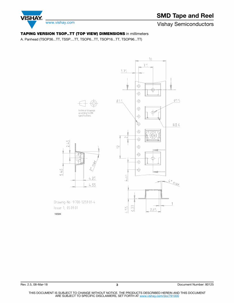
TAPING VERSION TSOP..TT (TOP VIEW) DIMENSIONS in millimetersA. Panhead (TSOP36...TT, TSSP....TT, TSOP6...TT, TSOP16...TT, TSOP96...TT)
16584
SMD Tape and Reelwww.vishay.com Vishay Semiconductors
Rev. 2.5, 08-Mar-18 4 Document Number: 80125
THIS DOCUMENT IS SUBJECT TO CHANGE WITHOUT NOTICE. THE PRODUCTS DESCRIBED HEREIN AND THIS DOCUMENTARE SUBJECT TO SPECIFIC DISCLAIMERS, SET FORTH AT www.vishay.com/doc?91000
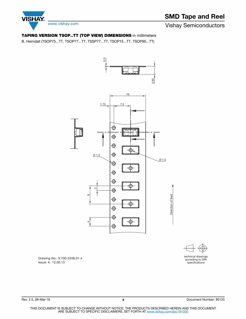
TAPING VERSION TSOP..TT (TOP VIEW) DIMENSIONS in millimetersB. Heimdall (TSOP75...TT, TSOP77...TT, TSSP77...TT, TSOP15...TT, TSOP95...TT)
0.3
3.65
16
7.51.75
Ø 1.5
Ø 1.5
2
84
Drawing-No.: 9.700-5338.01-4Issue: 4; 12.06.13
technical drawingsaccording to DINspecifications
Dire
ctio
n of
feed
SMD Tape and Reelwww.vishay.com Vishay Semiconductors
Rev. 2.5, 08-Mar-18 5 Document Number: 80125
THIS DOCUMENT IS SUBJECT TO CHANGE WITHOUT NOTICE. THE PRODUCTS DESCRIBED HEREIN AND THIS DOCUMENTARE SUBJECT TO SPECIFIC DISCLAIMERS, SET FORTH AT www.vishay.com/doc?91000
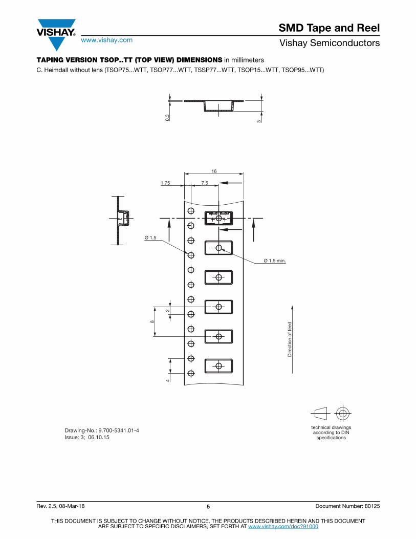
TAPING VERSION TSOP..TT (TOP VIEW) DIMENSIONS in millimetersC. Heimdall without lens (TSOP75...WTT, TSOP77...WTT, TSSP77...WTT, TSOP15...WTT, TSOP95...WTT)
2
1.75 7.5
16
8
4
30.3
Ø 1.5 min.
Ø 1.5
Drawing-No.: 9.700-5341.01-4Issue: 3; 06.10.15
technical drawingsaccording to DINspecifications
Dire
ctio
n of
feed

SMD Tape and Reelwww.vishay.com Vishay Semiconductors
Rev. 2.5, 08-Mar-18 6 Document Number: 80125
THIS DOCUMENT IS SUBJECT TO CHANGE WITHOUT NOTICE. THE PRODUCTS DESCRIBED HEREIN AND THIS DOCUMENTARE SUBJECT TO SPECIFIC DISCLAIMERS, SET FORTH AT www.vishay.com/doc?91000
TAPING VERSION TSOP..TT1 (TOP VIEW) DIMENSIONS in millimetersD. Belobog (TSOP37...TT1, TSOP57...TT1, TSOP17...TT1, TSOP97...TT1)
Tape and reel dimensions:
Parts mounted
Empty trailer 200 mm min.
Empty leader 400 mm min.
Direction of pulling out
Unreel direction
Ø 6
0 m
in.
Ø Y
2 ± 0.5
Label posted here
coming out from reelTape position
(12.4)
18.4 max.
Ø 13 ± 0.2Ø 21 ± 0.8
100 mm min. with cover tape
X 2:1
(2) (1.7
5)
(5.5
)
12 ±
0.3
(8) (4)(Ø 1.5)
(0.3)
(1.2)
Technical drawingsaccording to DINspecifications
Not indicated tolerances ± 0.1Drawing-No.: 9.700-5347.01-4Issue: 2; 07.03.18
Reel size “Y”TT1 Ø 180 ± 2 = 1800 pcs.
Leader and trailer tape:
SMD Tape and Reelwww.vishay.com Vishay Semiconductors
Rev. 2.5, 08-Mar-18 7 Document Number: 80125
THIS DOCUMENT IS SUBJECT TO CHANGE WITHOUT NOTICE. THE PRODUCTS DESCRIBED HEREIN AND THIS DOCUMENTARE SUBJECT TO SPECIFIC DISCLAIMERS, SET FORTH AT www.vishay.com/doc?91000
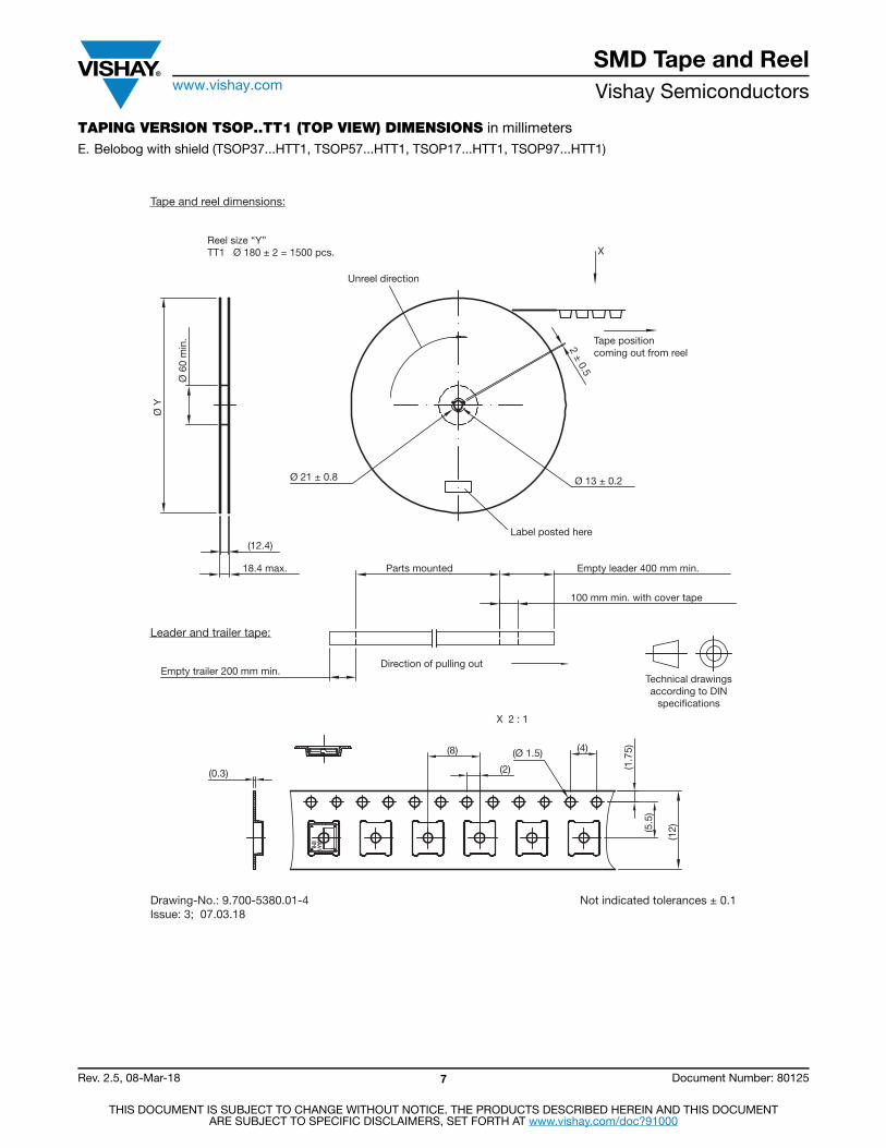
TAPING VERSION TSOP..TT1 (TOP VIEW) DIMENSIONS in millimetersE. Belobog with shield (TSOP37...HTT1, TSOP57...HTT1, TSOP17...HTT1, TSOP97...HTT1)
Reel size “Y”TT1 Ø 180 ± 2 = 1500 pcs.
Unreel direction
X
Tape positioncoming out from reel
2 ± 0.5
Ø 13 ± 0.2Ø 21 ± 0.8
Label posted here
Ø Y
Ø 6
0 m
in.
18.4 max.
(12.4)
Parts mounted Empty leader 400 mm min.
100 mm min. with cover tape
Direction of pulling outEmpty trailer 200 mm min.
X 2 : 1
(8)
(2)
(4)(Ø 1.5)
(1.7
5)
(0.3)
(5.5
)
(12)
Technical drawingsaccording to DINspecifications
Drawing-No.: 9.700-5380.01-4Issue: 3; 07.03.18
Not indicated tolerances ± 0.1
Tape and reel dimensions:
Leader and trailer tape:

SMD Tape and Reelwww.vishay.com Vishay Semiconductors
Rev. 2.5, 08-Mar-18 8 Document Number: 80125
THIS DOCUMENT IS SUBJECT TO CHANGE WITHOUT NOTICE. THE PRODUCTS DESCRIBED HEREIN AND THIS DOCUMENTARE SUBJECT TO SPECIFIC DISCLAIMERS, SET FORTH AT www.vishay.com/doc?91000
TAPING VERSION TSOP..DF1P (SIDE VIEW) DIMENSIONS in millimetersF. Minimold DF1P (TSOP33...DF1P, TSOP53...DF1P, TSOP13...DF1P, TSOP93...DF1P)
Drawing-No.: 9.800-5052.V3-4Issue: 1; 17.12.02
Form of the leave open of the wheel is supplier specific.Dimensions according to IEC EN 60 286-3
Tape width: 24
Technical drawingaccording to DINspecifications
Reel hub 2:1
Ø 20.2 min.
1.5
min
.
Ø 1
2.8
min
.
Ø 6
0 m
in.
24.4 +3
-0
Ø 3
30 +
0 -4
Drawing-No.: 9.700-5399.01-4Issue: 1; 30.06.16 (6.08)
(1.5 min.) (12)
(1.7
5)
(11.
5)
(24)
(2)(4) (1.55) (0.4)
(5.25)
(11.
75)
B
BAA B - B
A - A

SMD Tape and Reelwww.vishay.com Vishay Semiconductors
Rev. 2.5, 08-Mar-18 9 Document Number: 80125
THIS DOCUMENT IS SUBJECT TO CHANGE WITHOUT NOTICE. THE PRODUCTS DESCRIBED HEREIN AND THIS DOCUMENTARE SUBJECT TO SPECIFIC DISCLAIMERS, SET FORTH AT www.vishay.com/doc?91000
TAPING VERSION TSOP..TR (SIDE VIEW) DIMENSIONS in millimetersG. TVCastSMD TR1 (TSOP59...TR1, TSOP39...TR1, TSOP19...TR1, TSOP99...TR1)
A-A (2 : 1)
B-B (2 : 1)
A A
B
B
Dire
ctio
n of
feed
(1.75)(7.5)
(16)
(Ø 1)
(2)
(12)
(4)
Ø 1.5
(9.75)
(2.8
5)
(7.0
5)
1.7
()
Technical drawingsaccording to DINspecification.
Drawing-No.: GO-100220.10_ZIssue B: 08.02.17

SMD Tape and Reelwww.vishay.com Vishay Semiconductors
Rev. 2.5, 08-Mar-18 10 Document Number: 80125
THIS DOCUMENT IS SUBJECT TO CHANGE WITHOUT NOTICE. THE PRODUCTS DESCRIBED HEREIN AND THIS DOCUMENTARE SUBJECT TO SPECIFIC DISCLAIMERS, SET FORTH AT www.vishay.com/doc?91000
TAPING VERSION TSOP..TR (SIDE VIEW) DIMENSIONS in millimetersA. Panhead (TSOP36...TR, TSSP6...TR, TSOP6...TR, TSOP16...TR, TSOP96...TR)
16585

SMD Tape and Reelwww.vishay.com Vishay Semiconductors
Rev. 2.5, 08-Mar-18 11 Document Number: 80125
THIS DOCUMENT IS SUBJECT TO CHANGE WITHOUT NOTICE. THE PRODUCTS DESCRIBED HEREIN AND THIS DOCUMENTARE SUBJECT TO SPECIFIC DISCLAIMERS, SET FORTH AT www.vishay.com/doc?91000
TAPING VERSION TSOP..TR (SIDE VIEW) DIMENSIONS in millimetersB. Heimdall (TSSP7...., TSOP75...TR, TSOP77...TR, TSSP7....TR, TSOP15...TR, TSOP95...TR)
Drawing-No.: 9.700-5337.01-4Issue: 2; 06.10.15
2
1.75
7.5
16
8
4
3.6
0.3
Ø 1.5 min.
Ø 1.5
Dire
ctio
n of
feed
1.34 ref.
technical drawingsaccording to DINspecifications
SMD Tape and Reelwww.vishay.com Vishay Semiconductors
Rev. 2.5, 08-Mar-18 12 Document Number: 80125
THIS DOCUMENT IS SUBJECT TO CHANGE WITHOUT NOTICE. THE PRODUCTS DESCRIBED HEREIN AND THIS DOCUMENTARE SUBJECT TO SPECIFIC DISCLAIMERS, SET FORTH AT www.vishay.com/doc?91000
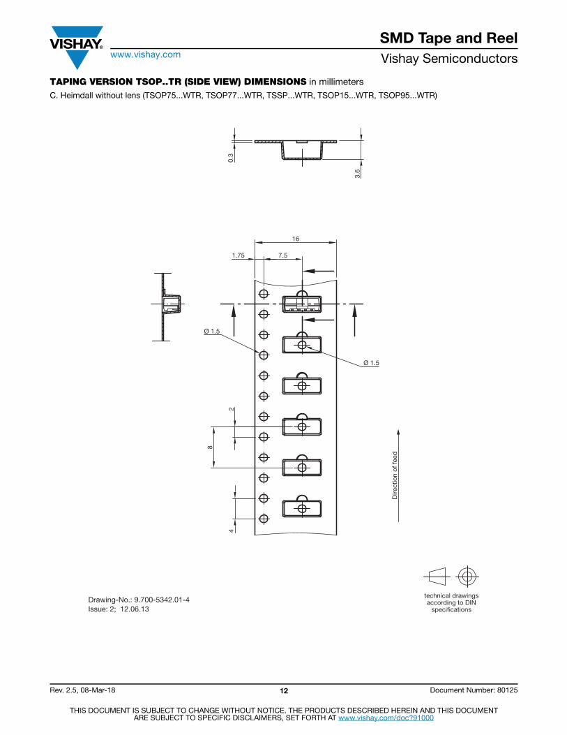
TAPING VERSION TSOP..TR (SIDE VIEW) DIMENSIONS in millimetersC. Heimdall without lens (TSOP75...WTR, TSOP77...WTR, TSSP...WTR, TSOP15...WTR, TSOP95...WTR)
2
1.75 7.5
16
8
4
3.6
0.3
Ø 1.5
Ø 1.5
Drawing-No.: 9.700-5342.01-4Issue: 2; 12.06.13
technical drawingsaccording to DINspecifications
Dire
ctio
n of
feed

SMD Tape and Reelwww.vishay.com Vishay Semiconductors
Rev. 2.5, 08-Mar-18 13 Document Number: 80125
THIS DOCUMENT IS SUBJECT TO CHANGE WITHOUT NOTICE. THE PRODUCTS DESCRIBED HEREIN AND THIS DOCUMENTARE SUBJECT TO SPECIFIC DISCLAIMERS, SET FORTH AT www.vishay.com/doc?91000
LEADER AND TRAILER DIMENSIONS in millimeters
COVER TAPE REEL STRENGTHAccording to DIN EN 60286-3
0.1 N to 1.3 N
300 mm/min. ± 10 mm/min.
165° to 180° peel angle
LABELStandard bar code labels for finished goods
The standard bar code labels are product labels and used for identification of goods. The finished goods are packed in final packing area. The standard packing units are labeled with standard bar code labels before transported as finished goods to warehouses. The labels are on each packing unit and contain Vishay Semiconductor GmbH specific data.
Trailer Leader
no devices
min. 200 min. 400
StartEnd
devices
96 11818
no devices
VISHAY SEMICONDUCTOR GmbH STANDARD BAR CODE PRODUCT LABEL (finished goods)PLAIN WRITING ABBREVIATION LENGTH
Item-description - 18
Item-number INO 8
Selection-code SEL 3
LOT-/serial-number BATCH 10
Data-code COD 3 (YWW)
Plant-code PTC 2
Quantity QTY 8
Accepted by ACC -
Packed by PCK -
Mixed code indicator MIXED CODE -
Origin xxxxxxx+ Company logo
LONG BAR CODE TOP TYPE LENGTH
Item-number N 8
Plant-code N 2
Sequence-number X 3
Quantity N 8
Total length - 21
SHORT BAR CODE TOP TYPE LENGTH
Selection-code X 3
Data-code N 3
Batch-number X 10
Filter - 1
Total length - 17

SMD Tape and Reelwww.vishay.com Vishay Semiconductors
Rev. 2.5, 08-Mar-18 14 Document Number: 80125
THIS DOCUMENT IS SUBJECT TO CHANGE WITHOUT NOTICE. THE PRODUCTS DESCRIBED HEREIN AND THIS DOCUMENTARE SUBJECT TO SPECIFIC DISCLAIMERS, SET FORTH AT www.vishay.com/doc?91000
DRY PACKAGINGThe reel is packed in an anti-humidity bag to protect the devices from absorbing moisture during transportation and storage.
RECOMMENDED METHOD OF STORAGEDry box storage is recommended as soon as the aluminum bag has been opened to prevent moisture absorption. The following conditions should be observed, if dry boxes are not available:
• Storage temperature 10 °C to 30 °C
• Storage humidity ≤ 60 % RH max.
After more than 72 h under these conditions moisture content will be too high for reflow soldering.
In case of moisture absorption, the devices will recover to the former condition by drying under the following condition:
192 h at 40 °C + 5 °C / - 0 °C and < 5 % RH (dry air / nitrogen) or 96 h at 60 °C + 5 °C and < 5 % RH for all device containers or 24 h at 125 °C + 5 °C not suitable for reel or tubes.
An EIA JEDEC® standard JSTD-020 level 4 label is included on all dry bags.
EIA JEDEC standard JSTD-020 level 4 label is includedon all dry bags
ESD PRECAUTIONProper storage and handling procedures should be followed to prevent ESD damage to the devices especially when they are removed from the antistatic shielding bag. Electrostatic sensitive devices warning labels are on the packaging.
VISHAY SEMICONDUCTORS STANDARD BAR CODE LABELSThe Vishay Semiconductors standard bar code labels are printed at final packing areas. The labels are on each packing unit and contain Vishay Semiconductors specific data.
OUTER PACKAGINGThe sealed reel is packed into a pizza box.
Aluminum bag
Label
Reel
15973
CAUTIONThis bag contains
MOISTURE-SENSITIVE DEVICES
1. Shelf life in sealed bag: 12 months at < 40 °C and < 90 % relative humidity (RH)
2. After this bag is opened, devices that will be subjected to soldering reflow or equivalent processing (peak package body temp. 260 °C) must be2a. Mounted within 72 hours at factory condition of < 30 °C/60 % RH or2b. Stored at < 5 % RH
3. Devices require baking befor mounting if: Humidity Indicator Card is > 10 % when read at 23 °C ± 5 °C or 2a. or 2b. are not met.
4. If baking is required, devices may be baked for: 192 hours at 40 °C + 5 °C/- 0 °C and < 5 % RH (dry air/nitrogen) or 96 hours at 60 °C ± 5 °C and < 5 % RH for all device containers or 24 hours at 125 °C ± 5 °C not suitable for reels or tubes
Bag Seal Date:(If blank, see barcode label)
Note: Level and body temperature defined by EIA JEDEC Standard J-STD-020
4LEVEL
22522
16962
CARTON BOX DIMENSIONS in millimeters
THICKNESS WIDTH LENGTH
Pizza box (SMD and heimdall)(taping in reels)
50 340 340
Thickness
Width 22127
Length
Legal Disclaimer Noticewww.vishay.com Vishay
Revision: 08-Feb-17 1 Document Number: 91000
DisclaimerALL PRODUCT, PRODUCT SPECIFICATIONS AND DATA ARE SUBJECT TO CHANGE WITHOUT NOTICE TO IMPROVE RELIABILITY, FUNCTION OR DESIGN OR OTHERWISE.
Vishay Intertechnology, Inc., its affiliates, agents, and employees, and all persons acting on its or their behalf (collectively, “Vishay”), disclaim any and all liability for any errors, inaccuracies or incompleteness contained in any datasheet or in any other disclosure relating to any product.
Vishay makes no warranty, representation or guarantee regarding the suitability of the products for any particular purpose or the continuing production of any product. To the maximum extent permitted by applicable law, Vishay disclaims (i) any and all liability arising out of the application or use of any product, (ii) any and all liability, including without limitation special, consequential or incidental damages, and (iii) any and all implied warranties, including warranties of fitness for particular purpose, non-infringement and merchantability.
Statements regarding the suitability of products for certain types of applications are based on Vishay’s knowledge of typical requirements that are often placed on Vishay products in generic applications. Such statements are not binding statements about the suitability of products for a particular application. It is the customer’s responsibility to validate that a particular product with the properties described in the product specification is suitable for use in a particular application. Parameters provided in datasheets and / or specifications may vary in different applications and performance may vary over time. All operating parameters, including typical parameters, must be validated for each customer application by the customer’s technical experts. Product specifications do not expand or otherwise modify Vishay’s terms and conditions of purchase, including but not limited to the warranty expressed therein.
Except as expressly indicated in writing, Vishay products are not designed for use in medical, life-saving, or life-sustaining applications or for any other application in which the failure of the Vishay product could result in personal injury or death. Customers using or selling Vishay products not expressly indicated for use in such applications do so at their own risk. Please contact authorized Vishay personnel to obtain written terms and conditions regarding products designed for such applications.
No license, express or implied, by estoppel or otherwise, to any intellectual property rights is granted by this document or by any conduct of Vishay. Product names and markings noted herein may be trademarks of their respective owners.
© 2017 VISHAY INTERTECHNOLOGY, INC. ALL RIGHTS RESERVED