Embed Size (px)
Citation preview
Indonesian Journal of Electrical Engineering and Computer Science
Vol. 16, No. 1, October 2019, pp. 299~310
ISSN: 2502-4752, DOI: 10.11591/ijeecs.v16.i1.pp299-310 299
Journal homepage: http://iaescore.com/journals/index.php/ijeecs
Practical understanding of the operating principle of digital
communication systems
Gebrehiwet Gebrekrstos Lema1, Teklehaymanot Baweke Reda2, Dawit Hadush Hailu3, Tole Sutikno4 1,2,3Ethiopian Institute of Technology-Mekelle, School of Electrical and Computer Engineering,
Mekelle University, Ethiopia 4Department of Electrical Engineering, Universitas Ahmad Dahlan, Indonesia
Article Info ABSTRACT
Article history:
Received Jan 29, 2019
Revised Apr 28, 2019
Accepted May 12, 2019
There are many students and researchers who don’t deeply understand the
practical operating principle of digital communication system. Hence, in this paper, the digital communication system is studied with brief implementation of each block diagrams. In the system kit development, text and audio inputs are taken and encrypted with different encryption techniques including additive cipher, multiplicative cipher and affine ciphers. The encrypted data is converted in to 8-bit binary data stream. Then, the channel is encoded with distinct channel coding techniques including linear block encoder, cyclic encoder and convolutional encoder. The line coded bits are band passed by digital modulation schemes after the channel coding. Finally, the developed
software is tested with equivalent inputs of a digital TV broadcasting and the results have correctly matched according to the theoretical analysis of the digital communication systems. Hence, students can be easily benefited from this practical understanding of the digital communication systems.
.
Keywords:
Channel coding
Digital communication
Line coding
Source coding
Copyright © 2019 Institute of Advanced Engineering and Science. All rights reserved.
Corresponding Author:
Gebrehiwet Gebrekrstos Lema, Department of Electrical and Computer Engineering,
Mekelle University,
Mekelle, Tigray, Ethiopia.
Email: [email protected]
1. INTRODUCTION
This digital communication simulation software is a tool for practical learning applications in campus
and it may also be used in practical transmission and reception of digital signals if modified somehow. In our
country students are mostly worried about where they can practice what they have learnt in class. Because there
is shortage of electronics components to practice in lab and see how it practically works. And due to this reason
students have limited understanding of digital communication system and its application.
The growing of demand for the huge data transmission made the digital communication systems
increasingly attractive. The fastest growing area in communication engineering is the design and manufacturing of hardware and software for digital communication networks [1]. It is proven that digital signals can be coded
to produce extremely low error rates and high fidelity [2]. Figure 1 shows the digital communication system
block diagram.
Some bits can corrupt in the noisy channel and might get interference through transmission over the
communication channel and the received signal will be demodulated into binary bits [3]. Hence, new kinds of
code, and new decoding methods, have recently been developed and are starting to be applied [4]. Among the
most sophisticated coding technique applied to the system can convert a noisy channel into an error-free
channel [5]. Error-free transmission is done by applying a coding technique of a random nature [6].
ISSN: 2502-4752
Indonesian J Elec Eng & Comp Sci, Vol. 16, No. 1, October 2019 : 299 - 310
300
Source encoder and decoder have been designed without knowledge about the statistical channel
encoder and decoder [7]. The idea of jointly designing the source-channel coding, begun with the work of [8].
It has been reported that, in noisy channels the design of joint source-channel encoder and decoder can improve
the performance dramatically. Digital communication has led to invent the social networking by three
important applications of digital which represented by: the internet- World Wide Web, mobile communication,
and satellite communication [9].
Figure 1. Digital communication system block diagram
However, the practical simulation and testing the operational principles of the digital communication
systems is not clearly verified in all the literatures. To the best of our knowledge there is no research that
discusses the practical understanding of the principles of the digital communications systems.
This project on digital communication simulator almost completely solves the above problem.
Obviously, electronics devices are more sensitive to damage during test in lab if the user makes a little mistake. This increases the cost of making and implementing the project. But this simulator kit takes no extra cost for
design and development except we used a computer to develop it. This is a kind of fool proof project which
you can’t use it wrongly.
Digital communication simulator software simulates most of the basic blocks of digital
communication systems. This simulator kit only processes text and audio files but if the size of the audio file
is large channel coding and channel decoding will take large time or probably the pc may stack.
To design a digital communication, a stabilization conditions were used [10] to design a secure digital
communization of a wide class of discrete-time hyperchaotic system via a scalar transmitted signal. Similarly,
a new chaotic secure digital communication scheme was proposed [11] based on chaotic Duffing oscillators
and frequency estimation for the transmission of binary-coded messages. However, they didn’t exploit the
channel coding mechanisms to make the digital communication inclusive. In digital communication, chaotic systems composed of multi-scroll attractors are preferred to the
double-scroll attractors because they offer more dynamical complexity [12-14]. In order to transmit high data
rate, the chaotic attractors are recommended to operate at high frequency. However, it is difficult to enhance
the frequency response of chaotic oscillator when it is designed with integrated circuit technology.
Synchronization is also made extended to complexity to the topologies with multi-scroll attractors [15, 16].
The main objective of this project is to make sure that students have broad understanding of the basic
blocks of digital communication systems and information theory and coding through practical simulations.
And the specific objective of this project work includes:
a. To study the principles of different kinds of encryption and decryption methods
b. To examine the formatting technique
c. To see how the different types of channel coding work and see their performance related to band width.
d. To observe the different types of line coding and decoding techniques. e. To study the behavior of base band modulation and demodulation techniques.
f. To see how error detected and corrected if any at the receiver using the following algorithms.
Indonesian J Elec Eng & Comp Sci ISSN: 2502-4752
Practical understanding of the operating principle of digital… (Gebrehiwet Gebrekrstos Lema)
301
In developing this software, we use the c sharp programming language as a tool. In developing this
software of digital communication simulation, we use the substitution method of encryption in the encryption
block. For the channel coding and decoding we use the systematic linear block codes. In the band pass
demodulation/detection also we include only the coherent detection method.
2. FUNDAMENTALS OF DIGITAL COMMUNICATIONS
In this paper, we present the basic principles that underlie the analysis and design of digital
communication systems. The subject of digital communication involves the transmission of information in
digital form from source that generates the information to one or more destinations. The sequences of binary digits from the source encoder are passed to the channel encoder. The purpose
of channel encoder is to introduce, in a controlled manner, some redundancy in the binary information sequence
that can be used at the receiver to overcome the effects of noise and interference encountered in the transmission
of the signal through the channel. Thus, the added redundancy serves to increase the reliability of the received
data and improves the fidelity of the received signal. In this case if k bits of message bits are channel encoded
in to n bits the rate of the code will be k/n.
The binary sequence at the output of the channel encoder is passed to the digital modulator, which
serves as the interface to the communication channel. Since nearly all of the communication channels
encountered in practice are capable of transmitting electrical signals (wave forms), the primary purpose of the
digital modulator is to map the binary information sequence in to signal wave forms. The digital modulator
may simply map the binary digit 0 into a waveform 𝑠0(t) and the binary digit 1 into a waveform 𝑠1(t). In this manner each bit from the channel encoder is transmitted separately. We call this binary modulation.
Alternatively, the modulator may transmit b coded information bits at a time by using M=2𝑏 distinct waveforms
𝑠𝑖(t), 𝑖 = 0, 1,… ,𝑚 − 1, one wave form for each of the 2𝑏 possible b-bit sequences. This type of modulation we call M-array modulation.
The communication channel is the physical medium that is used to send the signal from the transmitter
to the receiver. In wireless transmission, the channel may be the atmosphere (free space). On the other hand,
telephone channels usually employ a variety of physical media, including wire lines, optical fiber cables, and
wireless (microwave radio). Whatever the physical medium used for transmission of the information, the
essential feature is that the transmitted signal is corrupted in a random manner by a variety of possible
mechanisms, such as additive thermal noise generated by electronic devices, man-made noise, and atmospheric
noise.
At the receiving end of a digital communications system, the digital demodulator processes the
channel-corrupted transmitted waveform and reduces the waveforms to a sequence of numbers that estimates
of the transmitted data symbols (binary or M-array). This sequence of numbers is passed to the channel decoder, which attempts to detect and correct errors and reconstruct the original information sequence from knowledge
of the code used by the channel encoder and the redundancy contained in the received data.
A measure of how well the demodulator and decoder perform is the frequency with which errors occur
in the decoded sequence. More precisely, the average probability of a bit-error at the output of the decoder is a
measure of the performance of the demodulator-decoder combination. As a final step, when non-digital output
is desired, the source decoder accepts sequences of binary signals from the channel decoder and reconstructs
the original encrypted signal. The decryption block accepts the encrypted signal and deciphered the signal to
get the original transmitted message. In the following subtitles we are going to see the concepts and algorithms
of each block
2.1. Information source Information source is the original message given to a digital communication system as an input. The
message source can possibly be text, video, audio and digital data like computer output.
2.2. Encryption
Encryption is the process of hiding data to protect from external hackers. There are two types of
encryption called binary and text ciphers. But in this article, we will see the substitution cipher or encryption
which is text ciphering. Substitution cipher used to hide our data by replacing the characters in our plaintext
by another characters. But the replacement is takes place systematically. Additive cipher, multiplicative cipher
and affine cipher are the frequently used substitution method ciphers. Let’s see the algorithms one by one.
Additive cipher: An additive cipher is a substitution cipher. The letters of the plaintext stay in the
correct position but are replaced by other letters.
ISSN: 2502-4752
Indonesian J Elec Eng & Comp Sci, Vol. 16, No. 1, October 2019 : 299 - 310
302
Multiplicative cipher: It is substitution ciphers, but letters are replaced by multiplication. Modular
arithmetic becomes more obviously necessary here. The trickiest part is finding the multiplicative inverse in
the modular system.
Affine cipher: Affine ciphers are another variation of substitution cipher. This time, we combine both
additive and multiplicative steps. When encoding, add first, and then multiply. When decoding, multiply first
by the multiplicative inverse (t-1), then add the additive inverse (m-1).
2.3. Source encoder and decoder Source encoding is the process of converting asci code of the array of characters in to binary
equivalent. The source encoder block accepts the encrypted data from the encryption block and converts each
character to asci 8 or asci 7. The source decoding is the process of converting the binary bits into the asci
equivalent. The conversion process takes place by the following algorithm. Let we have an 8 bit array 𝑎 =[𝑎1 𝑎2 𝑎3 𝑎4 𝑎5 𝑎6 𝑎7 𝑎8] . Then, the asci equivalent will be:
𝑎𝑠𝑐𝑖 = 𝑎1 + 𝑎2 ∗ 2 + 𝑎3 ∗ 4 + 𝑎4 ∗ 8 + 𝑎5 ∗ 16 + 𝑎6 ∗ 32 + 𝑎7 ∗ 64 + 𝑎8 ∗ 128
2.4. Channel encoder and Channel decoding
Channel coding is often used in digital communication systems to protect the digital information from noise and interference and reduce the number of bit errors. Channel coding is mostly accomplished by
selectively introducing redundant bits in to the transmitted information stream. These additional bits will allow
detection and correction of bit errors in the received data stream and provide more reliable information
transmission. The cost of using channel coding to protect the information is a reduction in data rate or expansion
in bandwidth. There are two main types of channel codes, namely block codes and convolutional codes. The
block codes accept a block of k information bits and produce a block of n coded bits. By predetermined rule,
n-k redundant bits are added to the k information bits to form the n coded bits. Commonly these codes are
referred to us (n, k) block codes. Some of the commonly used block codes are linear block codes and cyclic
block codes. The convolutional coding encodes the sequence of message bits bit by bit instead of taking blocks
of bits.
Channel decoding is the process of recovering the transmitted bits from the channel encoder block. Channel decoding involves receiving the channel codeword with its possible channel noise, error detection
location and correcting if any. If no errors are found, the received block is taken as the errorless channel codes.
Depending on the transmitter encoder, there are adopted corresponding decoding schemes. In the following
subtitles we will see the details of the following channel coding and decoding types.
Linear block coding: Linear block encoder accepts binary data from the source encoder and segments
it in to message blocks of length k bits denoted by U. the message blocks are then encoded by adding n-k parity
bits to produce an n bit length codeword denoted by V. there are a total of 2k distinct messages. The encoder
according to certain rules transforms each input message u in to n bit V with 𝑛 > 𝑘. Corresponding to the 2k
possible messages, there are 2k code words called code word. An encoder which takes m bits and encode them
to n bits is called (𝑛, 𝑘) encoder. .The sequence of message and code word bits is given as follows:
𝑈 = [𝑢1, 𝑢2,𝑢3,−−−,𝑢𝑘]
𝑉 = [𝑣1,𝑣2, 𝑣3,−−−,𝑣𝑛]
The codeword V is generated by matrix multiplication of a generator matrix with the input vector U. Generator
matrix is an important parameter and it has two parts called the parity bit and information bit parts.
𝐺 = [𝑝𝑘𝑥𝑛−𝑘 : 𝐼𝑘𝑥𝑘]
The parity bit is represented by 𝑝𝑘𝑥𝑛−𝑘 and it is found by dividing 𝑥𝑛−𝑘+𝑖 to the generator polynomial
𝑔(𝑥) for 𝑖 = 0,1,… , 𝑘 − 1 and taking the remainder coefficients. The information part is represented by 𝐼𝑘𝑥𝑘
and is 𝑘 𝑏𝑦 𝑘 identity matrix. The generator polynomial should by a primitive with degree 𝑛 − 𝑘. Then the
resulting generator matrix will be
Indonesian J Elec Eng & Comp Sci ISSN: 2502-4752
Practical understanding of the operating principle of digital… (Gebrehiwet Gebrekrstos Lema)
303
𝐺 =
[ 𝑝11 𝑝11 … 𝑝1(𝑛−𝑘) : 1 0 … 0 0
𝑝21 𝑝22 … 𝑝2(𝑛−𝑘) : 0 1 … 0 0. . . . : . . … . .. . . . : . . … . .
𝑝(𝑘−1)1 𝑝(𝑘−1)2 … 𝑝(𝑘−1)(𝑛−𝑘) : 0 0 … 1 0
𝑝(𝑘)1 𝑝(𝑘)2 … 𝑝𝑘(𝑛−𝑘) : 0 0 … 0 1]
The encoding process takes place by multiplying each k message bits with the generator matrix as follows.
𝑽 = 𝑼 ∗ 𝑮
Let 𝑢 = [𝑢1, 𝑢2,… ,𝑢𝑘] be the message to be encoded and let 𝑣 = [𝑣1,𝑣2, 𝑣3,−−−,𝑣𝑛] be the encoded codeword.
Then:
𝑽 = [𝑢1, 𝑢2,… , 𝑢𝑘]
[ 𝑝11 𝑝12 … 𝑝1(𝑛−𝑘) : 1 0 … 0 0
𝑝21 𝑝22 … 𝑝2(𝑛−𝑘) : 0 1 … 0 0. . . . : . . … . .. . . . : . . … . .
𝑝(𝑘−1)1 𝑝(𝑘−1)2 … 𝑝(𝑘−1)(𝑛−𝑘) : 0 0 … 1 0
𝑝(𝑘)1 𝑝(𝑘)2 … 𝑝𝑘(𝑛−𝑘) : 0 0 … 0 1]
Linear block decoding: In this decoding we have useful parity check matrix (H matrix) which helps
to know if the received codes are generated from the generator matrix G. for each (𝑛, 𝑘) generator matrix G,
there exist an (𝑛 − 𝑘) × 𝑛 matrix H, such that the rows of G are orthogonal to the rows of H; that is, 𝐺𝐻𝑇 = 𝟎, where 𝐻𝑇is the transpose of H, and 0 is a 𝑘 × (𝑛 − 𝑘) all-zeros matrix.
𝐻𝑇 is an 𝑛 × (𝑛 − 𝑘) matrix whose rows are the columns of H and whose columns are the rows of H. To fulfill the orthogonality requirements for a systematic code, the components of the H matrix are written
as:
𝐺 =[𝑝𝑘𝑥𝑛−𝑘:𝐼𝑘𝑥𝑘]
Then the H matrix is:
𝐻 = [𝐼𝑛−𝑘𝑥𝑛−𝑘: 𝑝𝑇𝑛−𝑘𝑥𝑘
]
Hence, the 𝐻𝑇 matrix is written as:
𝐻𝑇 = [
𝐼𝑛−𝑘𝑥𝑛−𝑘……………𝑝 𝑘×𝑛−𝑘
]
If the received codeword v is generated from the generator matrix G, then 𝑽 ∗ 𝑯𝑻 = 0 otherwise the
received codeword is in error. Syndrome calculation and error detection: Syndrome is the strength of a codeword against error or
noise. Syndrome is calculated as follows:
Given that a codeword v generated from generated matrix G is transmitted and r with potential noise is
received. Then:
𝒓 = 𝒗 + 𝒆
Where 𝒆 = 𝑒1, 𝑒2, … , 𝑒𝑛 is an error vector or error pattern introduced by the channel. There is a total of 2𝑛 − 1
potential nonzero error patterns in the space of 2𝑛 n-tuples. The syndrome of r is defined as:
𝑺 = 𝒓𝑯𝑻
ISSN: 2502-4752
Indonesian J Elec Eng & Comp Sci, Vol. 16, No. 1, October 2019 : 299 - 310
304
The syndrome is the result of a parity check performed on r to determine whether r is a valid member of the
codeword set. If the received codeword r is generated from G then the syndrome s has a value 0. If r contains
detectable errors, the syndrome has some nonzero value. The syndrome of r is seen to be:
𝑺 = (𝒗 + 𝒆)𝑯𝑻 = 𝒗𝑯𝑻 + 𝒆𝑯𝑻
However, 𝒗𝑯𝑻 = 0 for all members of the code word set. Therefore:
𝑺 = 𝒆𝑯𝑻
From the above equations we can conclude that whether performed on either a corrupted code vector
or on the error pattern that caused it, the syndrome is the same. An important property of linear block codes,
fundamental to the decoding process, is that the mapping between correctable error patterns and syndromes is one to one.
Error correction: We have detected a single error and have shown that the syndrome test performed
on either the corrupted codeword, or on the error pattern that caused it, yields the same syndrome. This should
be a clue that we not only can detect the error, but since there is one-to-one correspondence between correctable
error patterns and syndromes, we can correct such error patterns.
Let us arrange the 2𝑛 n-tuples that represent possible received vectors in array, called the standard
array, such that the first row contains all the codewords, starting with the all zeros codeword, and the first
column contains all the correctable error patterns. From the basic properties of linear codes, the all-zeros vector
must be a member of the codeword set. Each row, called a coset, consists of an error pattern in the first column,
called the coset leader, followed by the codewords corrupted by that error pattern.
If we take (7, 4) encoder with generator polynomial 𝑔(𝑥) = 1 + 𝑥 + 𝑥3 .then, we arrange the 27 =128 seven-tuples in a standard array. The valid codewords are the sixteen vectors in the first row, and the correctable error patterns are the seven nonzero coset leaders in the first column. Notice that all 1-bit error
patterns are correctable. So, decoding will be correct if, and only if, the error pattern caused by the channel is
one of the coset leader.
The syndromes value listed in the table at the last column are determined from the correctable error
sequence by computing :
𝑺 = 𝒆𝑯𝑻
The procedure for error correction and decoding proceeds as follows:
a. Calculate the syndrome of r using 𝑺 = 𝒓𝑯𝑻
b. Locate the coset leader (error pattern) e, whose syndrome equals 𝒓𝑯𝑻 c. This error patter is assumed to be the corruption caused by the channel.
d. The corrected received vector, or codeword, is identified as = 𝒓 + 𝒆 . we can say that we retrieve the valid
codeword by subtracting out the identified error.
Decoder implementation:When the code is short as in case of the (7, 4) code described in the above section, the decoder can be imple mented with simple circuitry. Consider the steps that the decoder must take:
(1) Calculate the syndrome, (2) locate the error pattern, and (3) perform modulo-2 addition of the error pattern
and the received vector (which removes the error). From the syndrome equation we can derive expression for
each of the syndrome digits in terms of the received codeword digits as:
𝑺 = 𝒓𝑯𝑻
𝑺 = [𝒓𝟏 𝒓𝟐 𝒓𝟑 𝒓𝟒 𝒓𝟓 𝒓𝟔 𝒓𝟕]
[ 1 0 00 1 00 0 11 1 00 1 11 1 11 0 1]
2.5. Line coding (baseband modulation)
The term digital baseband modulation is synonymous to line codes. These are methods to transfer a digital bit stream over an analog baseband channel (low pass channel) using a pulse train that is a discrete
number of signal levels. The terminology line coding originated in telephony with the need to transmit digital
information across a copper telephone line. more specifically, binary data over a digital repeated line. The most
Indonesian J Elec Eng & Comp Sci ISSN: 2502-4752
Practical understanding of the operating principle of digital… (Gebrehiwet Gebrekrstos Lema)
305
common line coding is NRZ-L, RZ, Manchester, Uni-polar RZ, Bi-polar RZ and alternative mark
inversion (AMI).
a) NRZ-L (non return to zero): a 1 and 0 are represented by pulse of equal amplitude with positive and
negative sign respectively.
b) RZ (on-off signaling): in this form, symbol ‘1’ is represented by transmitting a pulse of constant amplitude
for the entire duration of the symbol and symbol ‘0’ is represented by switching off the pulse.
c) Uni-polar RZ: a one is represented by half bit wide pulse and a zero is represented by the absence of a
pulse.
d) Bi-polar RZ: - the ones and zeros are represented by opposite level pulses that are half bit wide. That is a
pulse is present in each interval. e) AMI (alternative mark inversion): positive and negative pulses of equal amplitudes are used alternatively
for symbol ‘1’ and no pulse for symbol ‘0’.
f) Manchester: a symbol ‘1’ is sent by transmitting positive volt for the first half of the bit interval and
negative volt for the 2𝑛𝑑 half of bit interval. And the symbol ‘0’ is sent with the inverse signal.
2.6. Digital modulation and demodulation
Bandpass modulation: Digital modulation is the process by which digital symbols are transformed in
to waveforms that are compatible with the characteristics of the channel. In the case of baseband modulation,
the waveforms usually take the form of shaped pulses. But in the case of band pass modulation the shaped
pulses modulate a sinusoidal wave form called a carrier wave, or simply a carrier.
In any event, the modulation process involves shifting or keying the amplitude, frequency or phase of
the carrier in accordance with the incoming data. Thus, there are 3 basic digital modulation techniques.
a. Amplitude shift keying (ASK) b. Frequency shift keying (FSK)
c. Phase shift keying (PSK)
Amplitude shift keying (ASK): In this method the amplitude of the carrier assumes one of the two
amplitudes dependent on the logic states of the input stream. In ASK the modulated waveform may be
written as:
𝑣𝐴𝑆𝐾(𝑡) = {𝐴𝑐 cos𝑤𝑐𝑡 = √
2𝐸𝑏
𝑇𝑏cos𝑤𝑐𝑡 , 𝑖𝑛𝑝𝑢𝑡 = 1
0 , 𝑖𝑛𝑝𝑢𝑡 = 0
Where Eb = bit energy = 𝐴𝑐2∗𝑇𝑏
2
To generate binary ASK we have to represent the input binary signal in uni-polar form or on off signal. Phase
shift keying: The general analytic expression for PSK is:
𝑠𝑖(𝑡) = √2𝐸
𝑇cos[𝑤0𝑡 + 𝜙𝑖(𝑡)] 0 ≤ t ≤ T i= 1, …, M
Where the phase 𝜙𝑖(𝑡), will have M discrete values, typically given by
𝜙𝑖(𝑡) =2𝜋𝑖
𝑀 𝑖 = 1, … ,𝑀
For the binary PSK (BPSK) M is 2. The parameter E is symbol energy, T is symbol time duration,
and 0 ≤ t ≤ T. In BPSK modulations, the modulated data signal shifts the phase of the waveform 𝑠𝑖(𝑡) to one
of the two states, either zero or π (1800). To generate a binary PSK signal, we have to represent the input binary sequence in NRZ with constant
amplitude levels +√𝐸𝑏 and −√𝐸𝑏 for binary “1” and “0” respectively. The resulting NRZ signal and the
sinusoidal carrier𝜙1(𝑡), whose frequency constant are applied to a product modulator. Frequency shift keying: The general analytic expression for FSK modulation is:
𝑠𝑖(𝑡) = √2𝐸
𝑇cos(𝑤𝑖𝑡 + 𝜙) , 0 ≤ 𝑡 ≤ 𝑇, 𝑖 = 1, … ,𝑀
ISSN: 2502-4752
Indonesian J Elec Eng & Comp Sci, Vol. 16, No. 1, October 2019 : 299 - 310
306
Where the frequency term 𝑤𝑖 has M discrete values, and the phase term 𝜙 is an arbitrary constant. For the
binary FSK (BFSK) M is 2. The parameter E is symbol energy, T is symbol time duration, and 0 ≤ t ≤ T. In
BFSK modulations, the modulated data signal shifts the frequency of the waveform 𝑠𝑖(𝑡) to one of the two
frequency states; eitherƒ𝑐1𝑜𝑟 𝑓𝑐2.
𝑠𝐵𝐹𝑆𝐾(𝑥) =
{
√2𝐸
𝑇cos𝑤𝑐1𝑡 , 𝑓𝑜𝑟 𝑖𝑛𝑝𝑢𝑡 =
′ 1′ , 𝑤𝑐1 = 2𝜋ƒ𝑐1
√2𝐸
𝑇cos𝑤𝑐2𝑡 , 𝑓𝑜𝑟 𝑖𝑛𝑝𝑢𝑡 =
′ 0′ , 𝑤𝑐2 = 2𝜋𝑓𝑐2
To generate binary FSK we have to represent the input binary signal in ON-OFF signaling form. Then the
signal is applied to product modulator with two frequency ƒ𝑐1and 𝑓𝑐2 and the input to the 2𝑛𝑑 product modulator is inverted.
𝑠𝐵𝐹𝑆𝐾(𝑥) = 𝑑(𝑡)𝑐𝑜𝑠 𝑤𝑐1(𝑡) + 𝑑′(𝑡) cos𝑤𝑐2(𝑡)
𝑤ℎ𝑒𝑟𝑒 𝑑′(𝑡)𝑖𝑠 𝑖𝑛𝑣𝑒𝑟𝑠𝑒 of 𝑑(𝑡)
Band pass demodulation is the process of recovering what was transmitted to the channel considering
any possible distortions or corruptions of the signal. When the carrier exploits knowledge of the carrier’s phase
to detect the signals, the process is called coherent detection; when the receiver does not utilize such phase
reference information, the process is called noncoherent detection. In digital communications, the term
demodulation and detection are often used interchangeably, although demodulation emphasizes waveform
recovery, and detection entails the process of symbol decision. In this literature we are using the coherent
detection. In the following subtitles we will see the demodulation/detection processes for the ASK, PSK and FSK modulation types.
Binary detection in ASK: To detect the original binary sequence of 1’s and 0’s we apply the noisy
BASK signal 𝑥(𝑡) to a correlater, which is also supplied with a locally generated coherent reference signal
𝜙1(𝑡). The correlator output 𝑥1 is compared with a threshold of zero volt. If 𝑥1 >√𝐸𝑏
2, the receiver decides in
favor of symbol “1”. On the other hand, if 𝑥1 < √𝐸𝑏
2 it decides in favor of symbol “0”.
Binary detection in PSK: To detect the original binary sequence of 1’s and 0’s we apply the noisy
BPSK signal 𝑥(𝑡) to a correlater, which is also supplied with a locally generated coherent reference signal
𝜙1(𝑡). The correlater output 𝑥1 is compared with a threshold of zero volt. If 𝑥1 >0, the receiver decides in favor
of symbol “1”. On the other hand, if 𝑥1 < 0 it decides in favor of symbol “0”.
Binary detection in FSK: To detect the original binary sequence given the noisy received signal 𝑥(𝑡). It consists of two correlater with common input, which are supplied with locally generated coherent reference
signals 𝜙1(𝑡) and 𝜙2(𝑡). The correlater outputs are then subtracted one from the other, and the resulting
deference y, is compared with a threshold of zero volt. If 𝑦 > 0 then, receiver decides in favor of “1”. On the
other hand, if 𝑦 < 0 it decides in favor of “0”. If y is exactly zero, the receiver makes a random guess in favor of “1” or “0”.
3. RESULTS AND DISCUSSIONS
In the digital communication simulation software, each block accepts input from the preceding block
and also in some block some input parameters are required from the user. In this chapter we are going to discuss
the input and output parameters for each block. In order to facilitate the input of these parameters and follow
the flow of the simulation, the Graphical User Interface (GUI) is designed for convenience to the user. The
input parameter can both be entered from the GUI or from prepared user file.
The GUI has 2 parts called the transmitter and receiver part. When the user clicks at the block diagram tab the block diagram that we develop in our project are displayed in the GUI. And when the help tab
is clicked all the algorithms and definitions of each block will be displayed so that the students can remember
what they have learnt in class. Now we are going to see the input and output parameters for the transmitter and
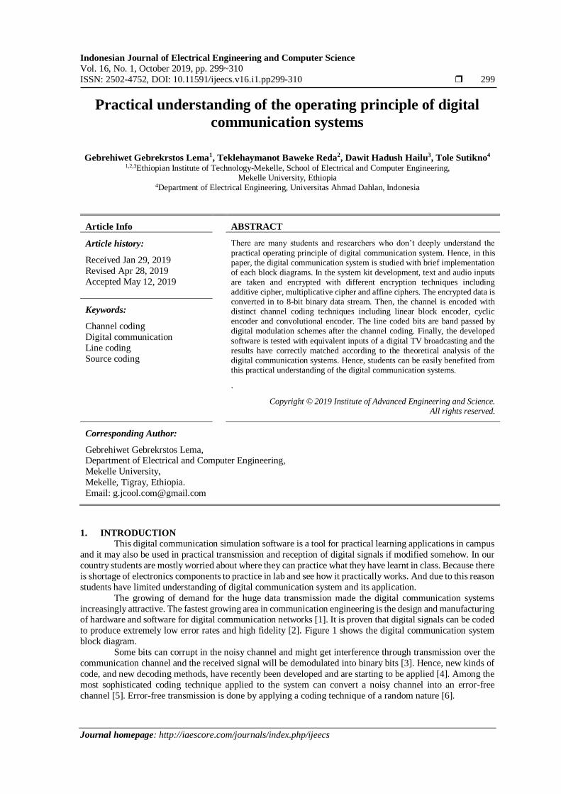
receiver. Have a look at the screen shot of the developed general block diagram of the graphical user interface
shown in Figure 2.
Indonesian J Elec Eng & Comp Sci ISSN: 2502-4752
Practical understanding of the operating principle of digital… (Gebrehiwet Gebrekrstos Lema)
307
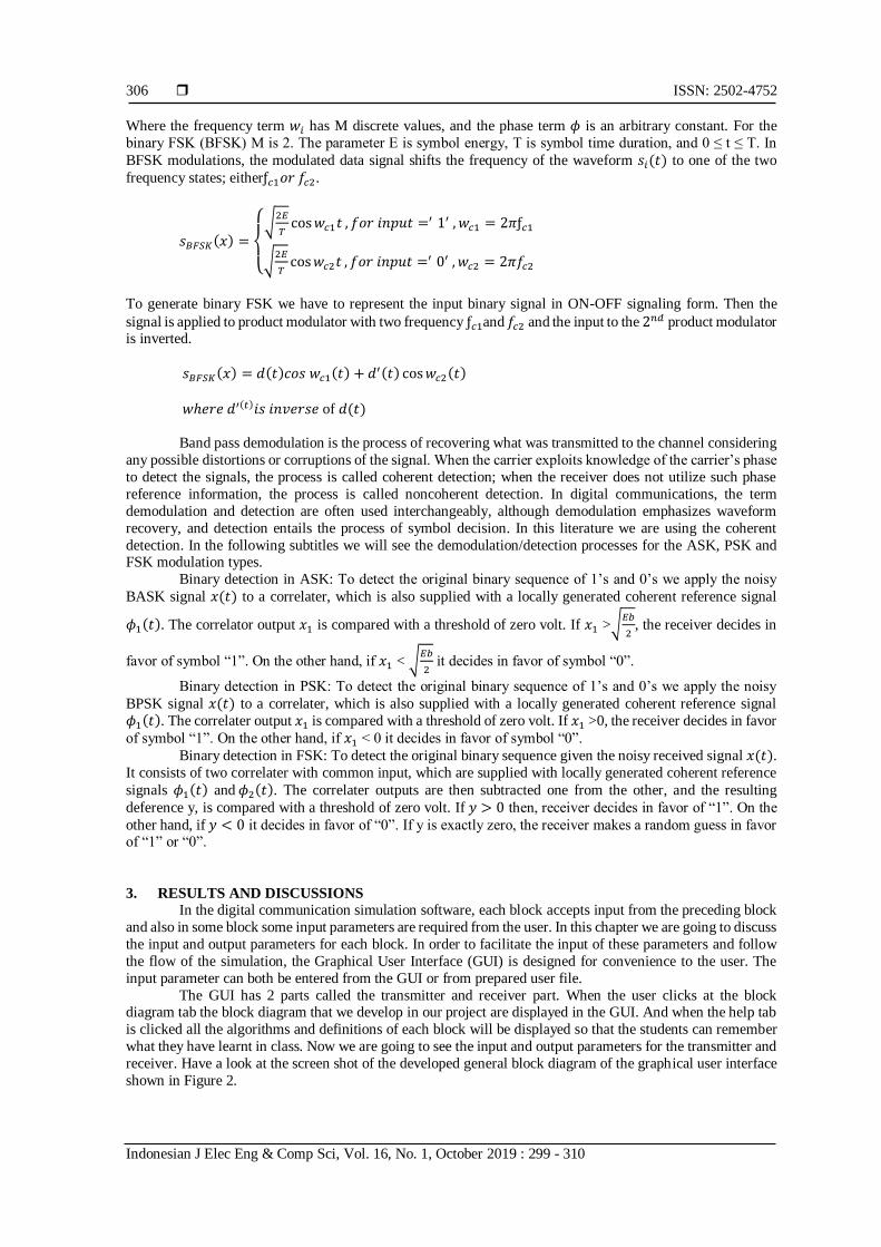
Figure 2. GUI of the secure digital communication
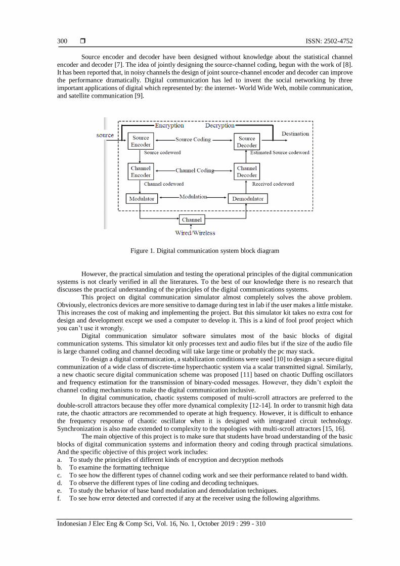
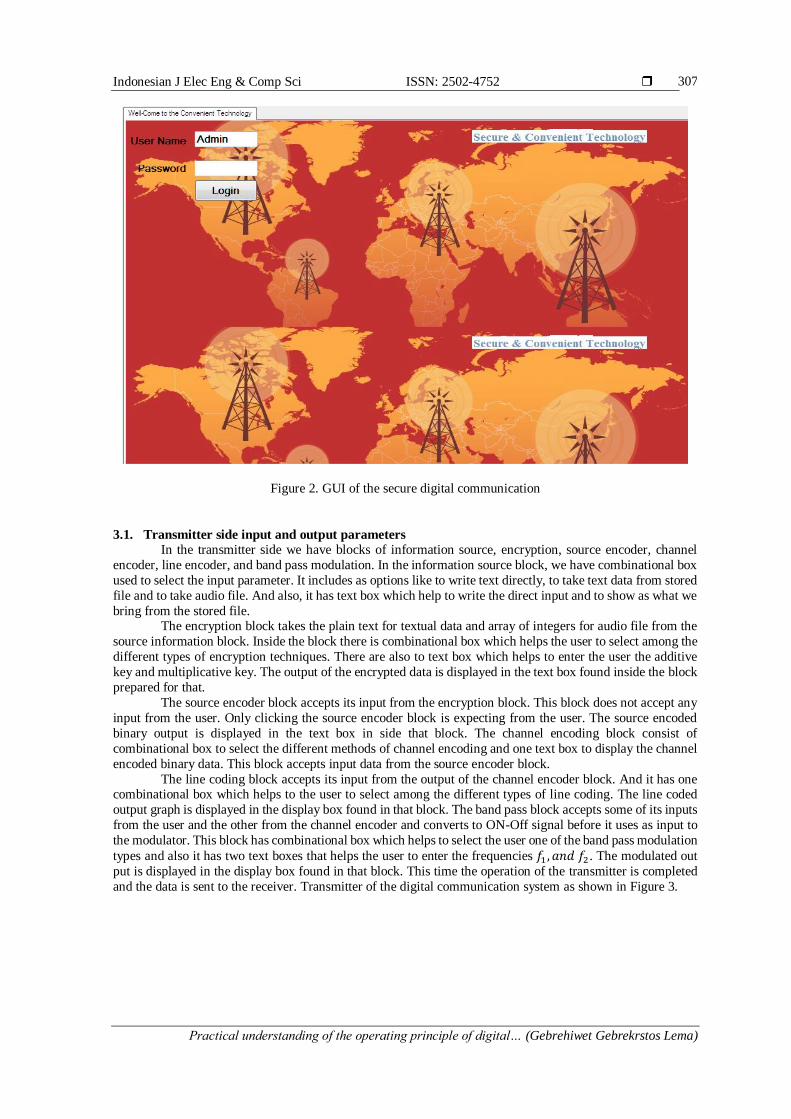
3.1. Transmitter side input and output parameters
In the transmitter side we have blocks of information source, encryption, source encoder, channel
encoder, line encoder, and band pass modulation. In the information source block, we have combinational box
used to select the input parameter. It includes as options like to write text directly, to take text data from stored
file and to take audio file. And also, it has text box which help to write the direct input and to show as what we
bring from the stored file. The encryption block takes the plain text for textual data and array of integers for audio file from the
source information block. Inside the block there is combinational box which helps the user to select among the
different types of encryption techniques. There are also to text box which helps to enter the user the additive
key and multiplicative key. The output of the encrypted data is displayed in the text box found inside the block
prepared for that.
The source encoder block accepts its input from the encryption block. This block does not accept any
input from the user. Only clicking the source encoder block is expecting from the user. The source encoded
binary output is displayed in the text box in side that block. The channel encoding block consist of
combinational box to select the different methods of channel encoding and one text box to display the channel
encoded binary data. This block accepts input data from the source encoder block.
The line coding block accepts its input from the output of the channel encoder block. And it has one combinational box which helps to the user to select among the different types of line coding. The line coded
output graph is displayed in the display box found in that block. The band pass block accepts some of its inputs
from the user and the other from the channel encoder and converts to ON-Off signal before it uses as input to
the modulator. This block has combinational box which helps to select the user one of the band pass modulation
types and also it has two text boxes that helps the user to enter the frequencies 𝑓1 , 𝑎𝑛𝑑 𝑓2 . The modulated out
put is displayed in the display box found in that block. This time the operation of the transmitter is completed
and the data is sent to the receiver. Transmitter of the digital communication system as shown in Figure 3.
ISSN: 2502-4752
Indonesian J Elec Eng & Comp Sci, Vol. 16, No. 1, October 2019 : 299 - 310
308
Figure 3. Transmitter of the digital communication system
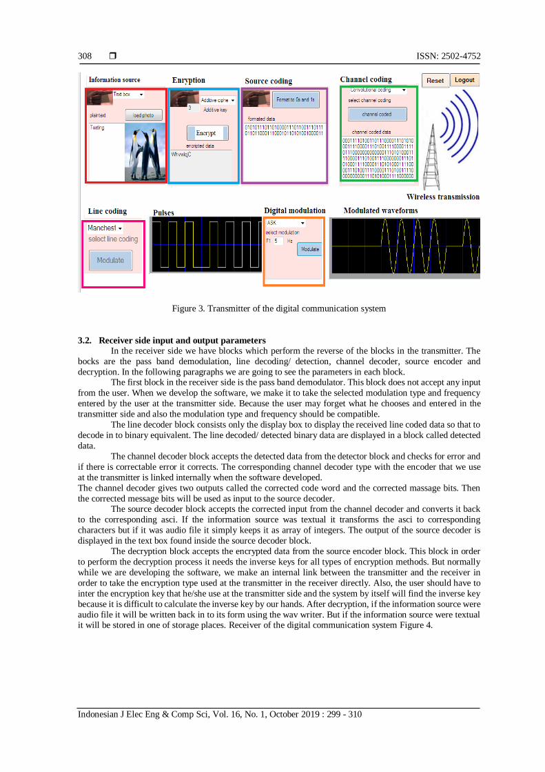
3.2. Receiver side input and output parameters
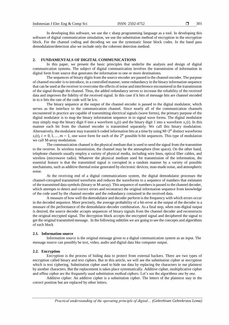
In the receiver side we have blocks which perform the reverse of the blocks in the transmitter. The
bocks are the pass band demodulation, line decoding/ detection, channel decoder, source encoder and
decryption. In the following paragraphs we are going to see the parameters in each block. The first block in the receiver side is the pass band demodulator. This block does not accept any input
from the user. When we develop the software, we make it to take the selected modulation type and frequency
entered by the user at the transmitter side. Because the user may forget what he chooses and entered in the
transmitter side and also the modulation type and frequency should be compatible.
The line decoder block consists only the display box to display the received line coded data so that to
decode in to binary equivalent. The line decoded/ detected binary data are displayed in a block called detected
data.
The channel decoder block accepts the detected data from the detector block and checks for error and
if there is correctable error it corrects. The corresponding channel decoder type with the encoder that we use
at the transmitter is linked internally when the software developed.
The channel decoder gives two outputs called the corrected code word and the corrected massage bits. Then
the corrected message bits will be used as input to the source decoder. The source decoder block accepts the corrected input from the channel decoder and converts it back
to the corresponding asci. If the information source was textual it transforms the asci to corresponding
characters but if it was audio file it simply keeps it as array of integers. The output of the source decoder is
displayed in the text box found inside the source decoder block.
The decryption block accepts the encrypted data from the source encoder block. This block in order
to perform the decryption process it needs the inverse keys for all types of encryption methods. But normally
while we are developing the software, we make an internal link between the transmitter and the receiver in
order to take the encryption type used at the transmitter in the receiver directly. Also, the user should have to
inter the encryption key that he/she use at the transmitter side and the system by itself will find the inverse key
because it is difficult to calculate the inverse key by our hands. After decryption, if the information source were
audio file it will be written back in to its form using the wav writer. But if the information source were textual it will be stored in one of storage places. Receiver of the digital communication system Figure 4.
Indonesian J Elec Eng & Comp Sci ISSN: 2502-4752
Practical understanding of the operating principle of digital… (Gebrehiwet Gebrekrstos Lema)
309
Figure 4. Receiver of the digital communication system
4. CONCLUSION AND RECOMMENDATION
In this project many digital communication system applications are used to develop the entire kit. Text
and audio inputs are taken, then this inputs are separately encrypted with different encryption techniques like
additive cipher, multiplicative cipher and affine ciphers, encrypted data is converted in to an 8 bit binary,
channel encoded with distinct channel coding styles like linear block encoder, cyclic encoder and convolutional
encoder, line coded with RZ, RZ_L, unipolar RZ, AMI, bipolar RZ and band pass modulated by ASK, FSK and PSK at the transmitter side and at the receiver side, band pass demodulation, line decoding, channel
decoding, reformatting and decryption corresponding to the transmitter side were taken. All the results found
are correct according to the theoretical analysis.
Further modification of this project is possible by adding some features like video input may be taken.
And it is also possible to use advanced encryption techniques to make the data transmission more secure than
ever. It is also good to add spread spectrum to this project to make it less prone to noise. Another channel
coding styles like BCH may also be used to see how the different channel coding methods differ and see which
is more secure to use and which is spectral efficient. The (7, 4) linear block encoder and cyclic encoder may
also be improved to correct more than one error by increasing the values of k and n compromising
system complexity.
ACKNOWLEDGMENT
We would like to acknowledge Hiliwi Leake Kidane who has designed the first draft of the project.
REFERENCES [1] Haykin, S. S., Moher, M., and Song, T., An introduction to analog and digital communications (Vol. 1). New York:
Wiley, 1989. [2] Kattoush, A., Digital communication. Dar Al-Manahej for Pub. & Distributing, Amman, 2005. [3] J. Li and K. Narayanan, “Rate-Compatible Low-Density Parity-Check Codes for Capacity-Approaching ARQ Scheme
in Packet Data Communications,” Int. Conf. on Comm., Internet, and Info. Tech. (CIIT), November 2002.
[4] Farahin Bt Tajul Arifin, N., Othman, N. S., and Ahmed, A. M., “Overcomplete source expansion aided, soft-bit assisted speech transceiver,” in Telecommunication Technologies (ISTT), 2014 IEEE 2nd International Symposium, pp. 326-329, November 2014.
[5] Nandan, S. and Deepthi, P. P., “Joint Source Channel Coding Using LDPC Codes,” in Computational Intelligence and Communication Networks (CICN), 2012 Fourth International Conference, pp. 355-358, November 2012.
[6] Carlson, A. B., Crilly, P. B., and Rutledge, J. C., Communication systems: an introduction to signals and noise in electrical communication. Guía Académica, p. 129. 1986.
[7] Ali, K., “An Enhanced Joint Source-Channel Decoder,” Doctoral dissertation, McGill University, 2005.
[8] Modestino, J. W. and Daut, D. G., “Combined source-channel coding of images,” Communications, IEEE Transactions, vol. 27(11), pp. 1644-1659, 1979.
ISSN: 2502-4752
Indonesian J Elec Eng & Comp Sci, Vol. 16, No. 1, October 2019 : 299 - 310
310
[9] Kaul, V., “The Digital Communications Revolution,” Online Journal of Communication and Media Technologies, vol. 2(3), p. 113, 2012. Kaul, V. (2012). The Digital Communications Revolution. Online Journal of Communication and Media Technologies, 2(3), 113.
[10] Filali R L, Benrejeb M, Borne P. On observer-based secure communication design using discrete-time hyperchaotic systems. Communications in Nonlinear Science and Numerical Simulation 2014, 19(5): 1424–1432.
[11] Zapateiro M, Vidal Y, Acho L. A secure communication scheme based on chaotic Duffing oscillators and frequency estimation for the transmission of binary-coded messages. Communications in Nonlinear Science and Numerical Simulation 2014, 19(4): 991–1003.
[12] Nunez J C, Tlelo E, Ramirez C, Jimenez J M. CCII plus Based on QFGMOS for Implementing Chua's Chaotic Oscillator. IEEE Latin America Transactions 2015, 13(9): 2865–2870.
[13] Fan L, Jun M. Pattern selection in network of coupled multi-scroll attractors. Plos One 2016, 11(4): 0154282. [14] Fan L, Cheng-Gui Y. The infinite-scroll attractor and energy transition in chaotic circuit. Nonlinear Dynamics 2016,
84: 2305–2315. [15] Soriano-Sanchez A G, Posadas-Castillo C, Platas-Garza M A, Cruz-Hernandez C, Lopez-Gutierrez R M. Coupling
strength computation for chaotic synchronization of complex networks with multi-scroll attractors. Applied Mathematics and Computation 2016, 275: 305–316
[16] Garza-Gonzalez E, Posadas-Castillo C, Rodriguez-Linan A. Chaotic synchronization of irregular complex network with hysteretic circuit-like oscillators in hamiltonian form and its application in private communications. Revista Mexicana De Fisica 2016, 62(1): 51–59.