Embed Size (px)
Citation preview
Industrial ApplicationsResearch Frontiers 2014Research Frontiers 2014 Research Frontiers 2014Research Frontiers 2014
90
Determining the operating principle of a three-terminal domain wall device
The rapid progress in magneto-resistive random access memory (MRAM) technologies provides non-volatile devices with high-speed operations, low power consumption, and high reliability. MRAM cells are based on magnetic tunnel junctions (MTJs) consisting of two ferromagnetic layers separated by a thin insulating layer. Parallel and antiparallel magnetic configurations of the MTJ induce low and high resistance states, which are defined as R0 and R1, respectively, due to the tunnel magnetoresistance (TMR) effect. Magnetization switching by the electric current through the MTJ or the ferromagnetic layer, such as spin-injection magnetization reversal [1] or current-induced domain wall (DW) motion [2], can be applied to write data in MRAM cells. Electrical manipulation of DWs is one candidate technique to write data to three-terminal MRAM cells with separate write and read current pathways.
Previously, we reported the development of a three-terminal DW device [3]. A low-current writing operation at 0.16 mA and a TMR of 80% were obtained for a 130-nm-wide free layer. The free layer, which is comprised of a CoFeB layer, with MgO capping and Ta seed layers, has a perpendicular magnetic anisotropy (PMA) and an excellent read property with a high TMR ratio [4]. However, the principle to write data in the DW device is unclear. An understanding of the operating principle is indispensable to further reduce the write current. In this article, the mechanism responsible for writing data in the device is derived from direct observations of DW motion in a Ta/CoFeB/MgO wire by means of photoemission electron microscopy with X-ray magnetic circular dichroism (XMCD-PEEM) and the electrical characteristics of the three-terminal DW device [5].
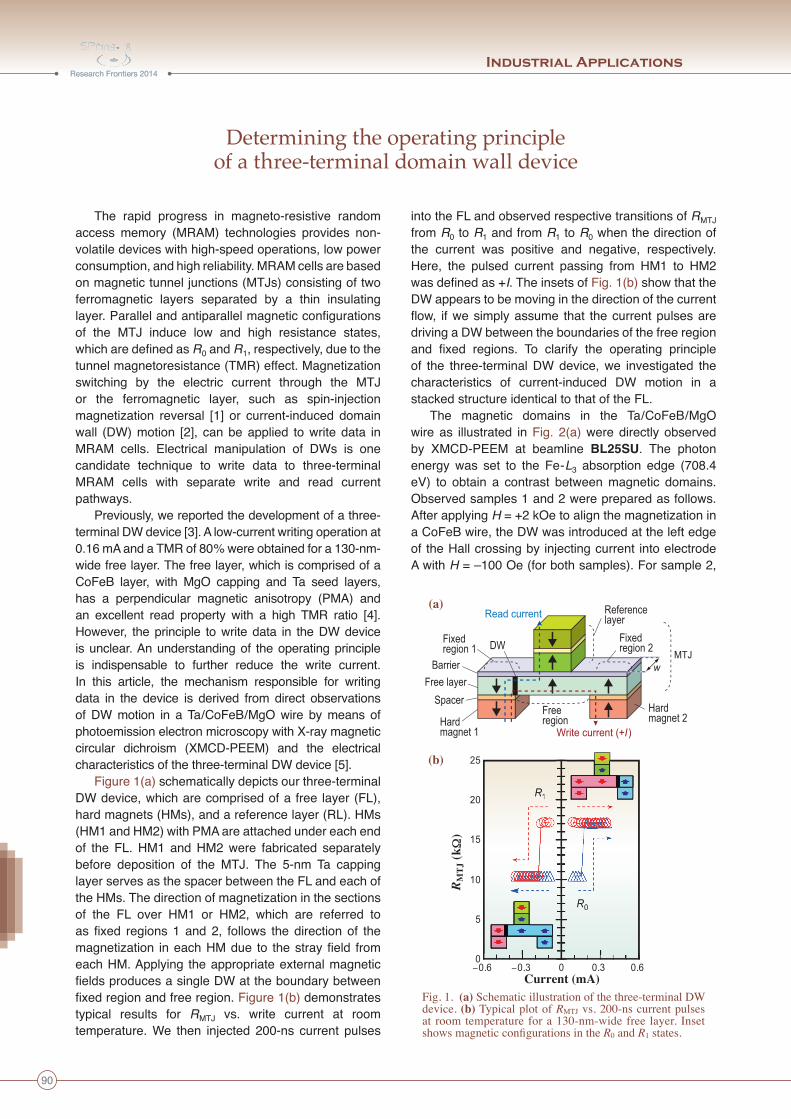
Figure 1(a) schematically depicts our three-terminal DW device, which are comprised of a free layer (FL), hard magnets (HMs), and a reference layer (RL). HMs (HM1 and HM2) with PMA are attached under each end of the FL. HM1 and HM2 were fabricated separately before deposition of the MTJ. The 5-nm Ta capping layer serves as the spacer between the FL and each of the HMs. The direction of magnetization in the sections of the FL over HM1 or HM2, which are referred to as fixed regions 1 and 2, follows the direction of the magnetization in each HM due to the stray field from each HM. Applying the appropriate external magnetic fields produces a single DW at the boundary between fixed region and free region. Figure 1(b) demonstrates typical results for RMTJ vs. write current at room temperature. We then injected 200-ns current pulses
into the FL and observed respective transitions of RMTJ from R0 to R1 and from R1 to R0 when the direction of the current was positive and negative, respectively. Here, the pulsed current passing from HM1 to HM2 was defined as +I. The insets of Fig. 1(b) show that the DW appears to be moving in the direction of the current flow, if we simply assume that the current pulses are driving a DW between the boundaries of the free region and fixed regions. To clarify the operating principle of the three-terminal DW device, we investigated the characteristics of current-induced DW motion in a stacked structure identical to that of the FL.
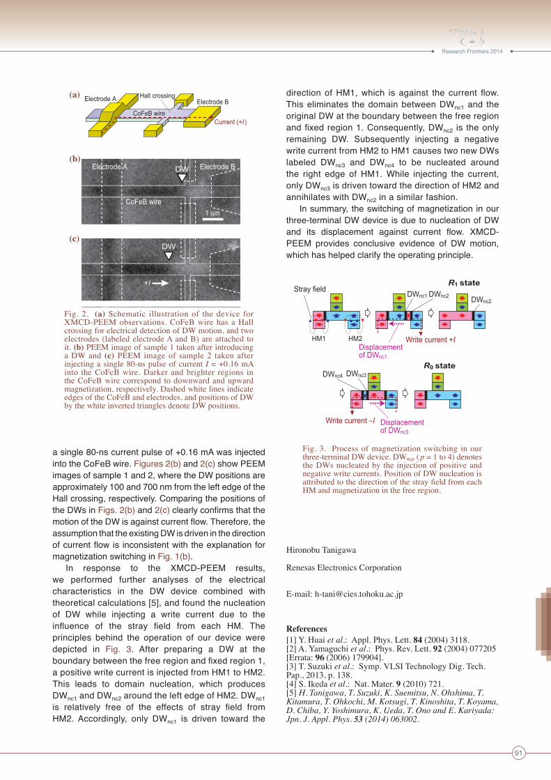
The magnetic domains in the Ta/CoFeB/MgO wire as illustrated in Fig. 2(a) were directly observed by XMCD-PEEM at beamline BL25SU. The photon energy was set to the Fe-L3 absorption edge (708.4 eV) to obtain a contrast between magnetic domains. Observed samples 1 and 2 were prepared as follows. After applying H = +2 kOe to align the magnetization in a CoFeB wire, the DW was introduced at the left edge of the Hall crossing by injecting current into electrode A with H = –100 Oe (for both samples). For sample 2,
Fig. 1. (a) Schematic illustration of the three-terminal DW device. (b) Typical plot of RMTJ vs. 200-ns current pulses at room temperature for a 130-nm-wide free layer. Inset shows magnetic configurations in the R0 and R1 states.
0
5
10
15
20
25
–0.6 –0.3 0 0.3 0.6
DWFixedregion 1
Hardmagnet 1
Hardmagnet 2
Referencelayer
Fixedregion 2
Freeregion
R MTJ
(kΩ
)
Current (mA)
R1
R0
(a)
(b)
Read current
Spacer
MTJwBarrier
Free layer
Write current (+I)
R1
R0
Industrial ApplicationsResearch Frontiers 2014Research Frontiers 2014 Research Frontiers 2014Research Frontiers 2014
91
a single 80-ns current pulse of +0.16 mA was injected into the CoFeB wire. Figures 2(b) and 2(c) show PEEM images of sample 1 and 2, where the DW positions are approximately 100 and 700 nm from the left edge of the Hall crossing, respectively. Comparing the positions of the DWs in Figs. 2(b) and 2(c) clearly confirms that the motion of the DW is against current flow. Therefore, the assumption that the existing DW is driven in the direction of current flow is inconsistent with the explanation for magnetization switching in Fig. 1(b).
In response to the XMCD-PEEM results, we performed further analyses of the electrical characteristics in the DW device combined with theoretical calculations [5], and found the nucleation of DW while injecting a write current due to the influence of the stray field from each HM. The principles behind the operation of our device were depicted in Fig. 3. After preparing a DW at the boundary between the free region and fixed region 1, a positive write current is injected from HM1 to HM2. This leads to domain nucleation, which produces DWnc1 and DWnc2 around the left edge of HM2. DWnc1 is relatively free of the effects of stray field from HM2. Accordingly, only DWnc1 is driven toward the
direction of HM1, which is against the current flow. This eliminates the domain between DWnc1 and the original DW at the boundary between the free region and fixed region 1. Consequently, DWnc2 is the only remaining DW. Subsequently injecting a negative write current from HM2 to HM1 causes two new DWs labeled DWnc3 and DWnc4 to be nucleated around the right edge of HM1. While injecting the current, only DWnc3 is driven toward the direction of HM2 and annihilates with DWnc2 in a similar fashion.
In summary, the switching of magnetization in our three-terminal DW device is due to nucleation of DW and its displacement against current flow. XMCD-PEEM provides conclusive evidence of DW motion, which has helped clarify the operating principle.
Fig. 2. (a) Schematic illustration of the device for XMCD-PEEM observations. CoFeB wire has a Hall crossing for electrical detection of DW motion, and two electrodes (labeled electrode A and B) are attached to it. (b) PEEM image of sample 1 taken after introducing a DW and (c) PEEM image of sample 2 taken after injecting a single 80-ns pulse of current I = +0.16 mA into the CoFeB wire. Darker and brighter regions in the CoFeB wire correspond to downward and upward magnetization, respectively. Dashed white lines indicate edges of the CoFeB and electrodes, and positions of DW by the white inverted triangles denote DW positions.
Fig. 3. Process of magnetization switching in our three-terminal DW device. DWncp (p = 1 to 4) denotes the DWs nucleated by the injection of positive and negative write currents. Position of DW nucleation is attributed to the direction of the stray field from each HM and magnetization in the free region.
Hironobu Tanigawa
Renesas Electronics Corporation
E-mail: [email protected]
References[1] Y. Huai et al.: Appl. Phys. Lett. 84 (2004) 3118.[2] A. Yamaguchi et al.: Phys. Rev. Lett. 92 (2004) 077205 [Errata: 96 (2006) 179904].[3] T. Suzuki et al.: Symp. VLSI Technology Dig. Tech. Pap., 2013, p. 138.[4] S. Ikeda et al.: Nat. Mater. 9 (2010) 721.[5] H. Tanigawa, T. Suzuki, K. Suemitsu, N. Ohshima, T. Kitamura, T. Ohkochi, M. Kotsugi, T. Kinoshita, T. Koyama, D. Chiba, Y. Yoshimura, K. Ueda, T. Ono and E. Kariyada: Jpn. J. Appl. Phys. 53 (2014) 063002.
DW
CoFeB wire
Electrode A Electrode B
1 μm
DW
+I
Electrode A Hall crossingElectrode B
Current (+I )CoFeB wire
(a)
(b)
(c)
Write current +I
Write current –I
HM1 HM2
Stray field
Displacementof DWnc1
Displacementof DWnc3
DWnc1 DWnc2
DWnc4 DWnc3
DWnc2
R1 state
R0 state