Embed Size (px)
Citation preview
ARMY TM 11-6130-417-14
NAVY EE010-BK-MMA-010/E154 PS30A
A I R F O R C E T.O. 35C1-2-848-1
T E C H N I C A L M A N U A L
OPERATOR’S,
ORGANIZATIONAL, DIRECT SUPPORT,
AND GENERAL SUPPORT MAINTENANCE MANUAL
FOR
P O W E R S U P P L Y P P - 7 8 3 3 / U( N S N - 6 1 3 0 - 0 0 - 2 4 9 - 2 7 4 8 )
DEPARTMENTS OF THE ARMY, NAVY. AND AIR FORCE
2 5 F E B R U A R Y 1 9 8 3
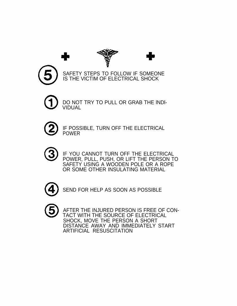
SAFETY STEPS TO FOLLOW IF SOMEONEIS THE VICTIM OF ELECTRICAL SHOCK
DO NOT TRY TO PULL OR GRAB THE lNDl-VIDUAL
IF POSSIBLE, TURN OFF THE ELECTRICALPOWER
IF YOU CANNOT TURN OFF THE ELECTRICALPOWER, PULL, PUSH, OR LIFT THE PERSON TOSAFETY USING A WOODEN POLE OR A ROPEOR SOME OTHER INSULATING MATERIAL
SEND FOR HELP AS SOON AS POSSIBLE
AFTER THE INJURED PERSON IS FREE OF CON-TACT WITH THE SOURCE OF ELECTRICALSHOCK, MOVE THE PERSON A SHORTDISTANCE AWAY AND IMMEDIATELY STARTARTIFICIAL RESUSCITATION
TM 11-6130-417-14/EE010-BK-MMA-010/E154 PS30A/T.O. 35C1-2-848-1
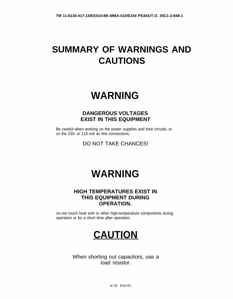
SUMMARY OF WARNINGS ANDCAUTIONS
WARNING
DANGEROUS VOLTAGESEXIST IN THIS EQUIPMENT
Be careful when working on the power supplies and their circuits, oron the 230- or 115-volt ac line connections.
DO NOT TAKE CHANCES!
WARNING
HIGH TEMPERATURES EXIST INTHIS EQUIPMENT DURING
OPERATION.
Do not touch heat sink or other high-temperature components duringoperation or for a short time after operation.
CAUTION
When shorting out capacitors, use aload resistor.
a/(b blank)

TECHNICAL MANUAL TM 11-6130-417-14NO. 11-6130-417-14 EE010-BK-MMA-010/E154 PS30ATECHNICAL MANUAL T.O. 35C1-2-848-1EE010-BK-MMA-0101/E154 PS30ATECHNICAL ORDER DEPARTMENTS OF THE ARMY,T.O. 35C1-2-848-1 THE NAVY, AND
THE AIR FORCE
Washington, DC, 25 February 1983
This manual contains copyright material reproduced by permission of the Hewlett-Packard Company.
OPERATOR’S, ORGANIZATIONAL, DIRECT SUPPORT, AND
GENERAL SUPPORT MAINTENANCE MANUAL
FOR
POWER SUPPLY PP-7833/U
(NSN-6130-00-249-2748)
REPORTING ERRORS AND RECOMMENDING IMPROVEMENTS
You can help improve this manual. If you find any mistakes or if you know ofa way to improve the procedures, please let us know. Mail your letter, DA Form2028 (Recommended Changes to Publications and Blank Forms), or DA Form2028-2 located in back of this manual direct to: Commander, US Army Com-munications Electronics Command and Fort Monmouth. ATTN: DRSEL-ME-MP,Fort Monmouth, New Jersey 07703.
For Air Force, submit AFTO Form 22 (Technical Order System PublicationImprovement Report and Reply) in accordance with paragraph 6-5, Section Vl,T.O. 00-5-1. Forward direct to prime ALC/MST.
For Navy, mail comments to the Commander, Naval Electronics Systems Com-mand, ATTN: ELEX 8122, Washington, DC 20360.
In either case, a reply will be furnished direct to you.
This manual is an authentication of the manufacturer’s commercial literature which, through usage, has beenfound to cover the data required to operate and maintain this equipment. Since the manual was not prepared inaccordance with military specifications and AR301-3, the format has not been structured to consider levels ofmaintenance.
i
TM 11-6130-417-14/EE010-BK-MMA-010/E154 PS30A/T.O. 35C1-2-848-1
TABLE OF CONTENTS
Section Page
I GENERAL INFORMATION1-A.11-A.3
1-A.4
1-A.5
1-A.61-A.8
1-A.101-11-81-101-12
1-15
1-171-19
SCOPE . . . . . . . . . . . . . . . . . . . . . . . . 1-1INDEX OF TECHNICAL
PUBLICATIONS . . . . . . . . . . . . . . 1-1MAINTENANCE FORMS, RECORDS
AND REPORTS . . . . . . . . . . . . . . 1-1REPORTING EQUIPMENT
IMPROVEMENTRECOMMENDATIONS . . . . . . . . . 1-1
ADMINISTRATIVE STORAGE . . . 1-2DESTRUCTION OF ARMY
ELECTRONICS MATERIEL . . . . 1-2PURPOSE AND USE . . . . . . . . . . . 1-2DESCRIPTION . . . . . . . . . . . . . . . . . 1-3SPECIFICATIONS . . . . . . . . . . . . . . 1-3OPTIONS . . . . . . . . . . . . . . . . . . . . . . 1-4lNSTRUMENT/MANUAL
IDENTIFICATION . . . . . . . . . . . . . 1-4ORDERING ADDITIONAL
MANUALS . . . . . . . . . . . . . . . . . . . 1-7EQUIPMENT SUPPLIED . . . . . . . . 1-7ACCESSORY EQUIPMENT
AVAILABLE . . . . . . . . . . . . . . . . . 1-7
II INSTALLATION . . . . . . . . . . . . . .2-12-32-52-72-92-112-132-15
2-17
2-20
2-22
2-24
2-26
2-28
2-30
2-1INITIAL INSPECTION. . . . . 2-1Mechanical Check . . . . . . . . 2-1Electrical Check . . . . . . . . . . . 2-1INSTALLATION DATA . . . . . . 2-1Location and Cooling . . . . . . . . 2-1Outline Diagram . . . . . . . . . . . . 2-1Rack Mounting . . . . . . . . . 2-1INPUT POWER
REQUIREMENTS . . . . . 2 -1INPUT LINE VOLTAGE OR
FREQUENCY CONVERSION . 2-2
Converting a Standard Instrument
to 208-Volt Operation (Models6259B, 6261B, and 6268B). . . 2-2
Converting a Standard Instrument
to 208-Volt Operation (Models6260B and 6269B). . . . . . 2-2
Converting a Standard Instrumentto 115-Volt Operation (Models
6259B, 6261B, and 6268B). . . 2-2Converting a Standard Instrument
to 115-Volt Operation (Model6260B) . . . . . . . . . . . . . 2-3
Converting a Standard Instrumentto 50Hz Operation . . . . . . . . 2-3
INPUT POWER CONNECTIONS . . 2-3
Section
2-32
2-342-36
Page
AC POWER CABLE STRAINRELIEF ASSEMBLY . . . . . . . . . . . . 2-4
INSTALLATION INSTRUCTIONS . . 2-4REPACKING FOR SHIPMENT . . . . . 2-4
III OPERATING INSTRUCTIONS . . 3-13-1
3-3
3-63-83-10
3-12
3-15
3-203-22
3-24
3-273-343-51
3-573-673-76
3-77
3-793-823-85
3-873-91
TURN-ON CHECKOUTPROCEDURE . . . . . . . . . 3-1
OPERATING MODES . . . . . 3-2NORMAL OPERATING MODE . . 3-2
Constant Voltage Operation . . . 3-2Constant Current Operation . . . . 3-2
Overvoltage Trip PointAdjustment . . . . . . . . . . . . . 3-2
Connecting The Load . . . . . . . 3-3
Operation With No Load . . . . . 3-3Operation Beyond Rated
Output . . . . . . . . . . . . . . 3-3OPTIONAL OPERATING
MODES . . . . . . . . . . . . . . . .3-3
Remote Voltage Sensing . . . . . 3-3Remote Programming . . . . . . . 3-5Auto-Parallel Operation . . . . . . 3-8Auto-Series Operation . . . . . . . 3-8Auto-Tracking Operation . . . . . 3-10SPECIAL OPERATING
CONSIDERATIONS . . . . . 3-12Pulse Loading . . . . . . . . . . . . . . 3-12
Output Capacitance . . . . . . . . . . 3-12Reverse Voltage Protection . . . . 3-12
Reverse Current Loading . . . . . 3-12Battery Charging . . . . . . . . . . . . 3-12Battery Discharging . . . . . . . . 3-13
IV PRINCIPLES OF OPERATION . . 4-14-1
4-16
4-17
4-274-294-31
4-334-404-45
4-484-524-584-614-664-70
OVERALL BLOCKDIAGRAM DISCUSSION . . . . 4-1
DETAILED CIRCUIT
ANALYSIS . . . . . . . . . . . . . 4-3Preregulator Control Circuit . . . . 4-3
Overvoltage Limit Circuit . . . . . . 4-4Series Regulator and Driver . . . . 4-4Short-Circuit Protection . . . . . . 4-4
Constant-Voltage Comparator . . . 4-4Constant-Current Comparator . . . 4-5Voltage Clamp Circuit . . . . . . . . 4-6Mixer and Error Amplifiers . . . . 4-6
Overvoltage Protection Crowbar . . 4-6Turn-On Control Circuit . . . . . . 4-7Reference Regulator . . . . . . . . . . 4-7Meter Circuit . . . . . . . . . . . . . . 4-7
Additional Protection Features . . 4-7
ii
TM 11-6130-417-14/EE010-BK-MMA-010/E154 PS30A/T.O. 35C1-2-848-1
TABLE OF CONTENTS (Continued)
Section Page
V MAINTAINANCE . . . . . . . . . . .
5-55-7
5-38
5-49
5-54
5-60
5-69
5-71
5-73
5-755-775-79
5-89
5-1INTRODUCTION . . . . . . . . . 5-1
TEST EQUIPMENT
REQUIRED . . . . . . . . . . 5-2PERFORMANCE TEST . . . . . 5-2
CONSTANT-VOLTAGE TESTS . . 5-2
CONSTANT-CURRENT TESTS . . 5-6TROUBLESHOOTING . . . . . . . . 5-8
OVERALL TROUBLE-
SHOOTING PROCEDURES . . 5-8Disassembly Procedures . . . . . . 5-15
REPAIR AND REPLACEMENT . 5-16
ADJUSTMENT AND
CALIBRATION . . . . . . . . . . 5-16Meter Zero Adjustment . . . . . . . 5-16
Voltmeter Calibration . . . . . . . 5-16
Ammeter Calibration . . . . . . . . 5-17
Constant-Voltage ProgrammingCalibration . . . . . . . . . . . . . . 5-17
Constant-Current Programming
5-98
5-1005-102
5-104
5-106
5-1085-110
Calibration . . . . . . . . . . . . . . 5-18Load Transient Recovery Time
Adjustment . . . . . . . . . . . . 5-19
Ripple Balance Adjustment . . . 5-19Preregulator Tracking
Adjustment . . . . . . . . . . . . . 5-20Crowbar Trip Voltage
Adjustment . . . . . . . . . . . . . 5-20Maximum Crowbar Trip
Voltage Adjustment . . . . . . . . 5-20Disabling the Crowbar . . . . . . . . . . . . 5-20
OVERHAUL AND REBUILD . . . . . . 5-21
Section
5-112
5-114
5-116
5-118
5-120
5-122
5-124
5-126
5-1285-130
5-132
5-1345-136
Page
Complete Removal of A3Interconnection Board . . . . . . . . . . 5-21
Complete Removal of A4
Heat Sink . . . . . . . . . . . . . . . . . . . . . 5-21Power Transformer T1
Removal . . . . . . . . . . . . . . . . . . . . . . 5-21
B2 Fan Removal . . . . . . . . . . . . . . . 5-21
Complete Removal of Main Filter
Capacitor Bank . . . . . . . . . . . . . . . . 5-21
B Bus Bars (+B, –B)
Removal . . . . . . . . . . . . . . . . . . . . . 5-21
Removal of Standoff Mounts For
A2 RFI Circuit Assembly . . . . . . . . 5-22Removal of Input Power
Terminal Board TB1 . . . . . . . . . . . 5-22
Removal of Rear Panel . . . . . . . . . . . 5-22
A5 Front Panel Removal . . . . . . . . . 5-22A5 Front Panel Disassembly . . . . 5-22
Complete Unit Disassembly . . . . . . . 5-23Unit Reassembly . . . . . . . . . . . . . . . . 5-23
VI CIRCUIT DIAGRAM AND COMPONENTLOCATION DIAGRAMS
AppendixA REFERENCES . . . . . . . . . . . . . . . . . . . . . . . . . A-1B MAINTENANCE ALLOCATION . . . . . . . . . . B-1C COMPONENTS OF END ITEM AND BASIC
ISSUE ITEMS LIST . . . . . . . . . . . . . . . . . . C-1D ADDITIONAL AUTHORIZATION LIST . . . . D-1E EXPENDABLE SUPPLIES AND
MATERIALS LIST . . . . . . . . . . . . . . . . . . . E-1
Index . . . . . . . . . . . . . . . . . . . . . . . . . . . . . . . . . . I-1
...III
TM 11-6130-417-14/EE010-BK-MMA-010/E154 PS30A/T.O. 35C1-2-848-1
LIST OF ILLUSTRATIONS
1-1
2-12-2
2-3
2-4
2-52-63-13-23-33-4
3-5
3-6
3-7
3-8
3-9
3-103-113-123-133-143-153-163-17
DC Power Supply (0-40V/0-30A) PP-7833/U, ModelHP6268B (NSN 6130-00-249-2748) . . . . . . . . . . . . 1-1
Outline Diagrams . . . . . . . . . . . . . . . . . . . . . . . . 2-1Bias Transformer A3T2 Primary Connections
for 208Vac Operation and115Vac Operation . . . . . . . . . . . . . . . . . . . . . 2-2
Power Transformer T2 Primaty Connections for208Vac and 115Vac Operation . . . . . . . . . . 2-3
Power Transformer T1 Primary Connections for208Vac Operation . . . . . . . . . . . . . . . . . . . . . 2-4
Power Cable . . . . . . . . . . . . . . . . . . . . . . . . . . . . . 2-5AC Power Cable Strain Relief Assembly .... 2-6Front Panel ControlS and Indicators . . . . . . . . 3-1Normal Strapping Panel . . . . . . . . . . . . . . . . . . . 3-2Remote Sensing . . . . . . . . . . . . . . . . . . . . . . . . . 3-4Resistance Programming of Output
Voltage . . . . . . . . . . . . . . . . . . . . . . . . . . . . . . 3-5Voltage Programming of Output Voltage
(Unit Gain) . . . . . . . . . . . . . . . . . . . . . . . . . . . 3-6Voltage Programming of Output Voltage
(Variable Gain) . . . . . . . . . . . . . . . . . . . . . . . . 3-6Resistance Programming of Output
Current . . . . . . . . . . . . . . . . . . . . . . . . . . . . . . . 3-7Voltage Programming of Output Current
(Fixed Gain) . . . . . . . . . . . . . . . . . . . . . . . . . . 3-7Voltage Programming of Output Current
(Variable Gain) . . . . . . . . . . . . . . . . . . . . . . . . 3-6Auto-Parallel Operation of Two Units . . . . . . . 3-8Auto-Parallel Operation of Three Units . . . . . . 3-9Auto-Series Operation of Two Units . . . . . . . . 3-10Auto-Series Operation of Three Units . . . . . . . 3-10Auto Tracking Operation of Two Units . . . . . . 3-11Auto Tracking Operation of Three Units . . . . . 3-12Battery Charging . . . . . . . . . . . . . . . . . . . . . . . . . 3-13Battery Discharging . . . . . . . . . . . . . . . . . . . . . . . 3-14
4-14-2
4-34-45-1
5-25-35-45-55-65-7
5-8
5-96-16-2
6-36-4
6-5
6-6
6-76-66-9FO-1
FO-2
FO-3
Overall Block Diagram . . . . . . . . . . . . . . . . . . . . 4-1
Operating Focus of a CV/CC Powersupply . . . . . . . . . . . . . . . . . . . . . . . . . . 4-2
Triac Phase Control of AC Input Amplitude . . 4-3Preregulator Ccntrol Circuit Waveforms . . . . . 4-4
Constant Voltage Load RegulationTest Setup . . . . . . . . . . . . . . . . . . . . . . . . . . . 5-2
Ripple Test Setup . . . . . . . . . . . . . . . . . . . . . . . . 5-3Noise Spike Measurement Test Setup . . . . . . 5-4
Load Transient Recovery Time Test Setup . . 5-5Load Transient Recovery Time Waveforms . . 5-6Current Sampling Resistor Connections . . . . . 5-7Constant-Current Load Regulation
Test Setup . . . . . . . . . . . . . . . . . . . . . . . . . . . 5-8
Constant-Current Ripple and NoiseTest Setup . . . . . . . . . . . . . . . . . . . . . . . . . . . 5-8
Zero Adjust Section of Main Circuit Board . . . 5-17A2 RFI Assembly Component Locations . . . . 6-1A3 Interconnection Board Component
Location . . . . . . . . . . . . . . . . . . . . . . . . . . . . . . 6-1Chassis Component Locations, Top View . . . 6-2Chassis Component Locations,
Bottom View . . . . . . . . . . . . . . . . . . . . . . . . . . 6-2A4 Heat Sink Assembly, Top and
Front View . . . . . . . . . . . . . . . . . . . . . . . . . . . . 6-3A4 Heat Sink Assembly, Bottom and
Rear View . . . . . . . . . . . . . . . . . . . . . . . . . . . . 6-3A1 Board Component Locations . . . . . . . . . . . 6-4Rear Panel . . . . . . . . . . . . . . . . . . . . . . . . . . . . . . 6-5Rear Side of Front Panel . . . . . . . . . . . . . . . . . . 6-5Models 6259B, 6260B, 6261B, 6268B, and
6269B Schematic Diagram . . . . . . . . . . . . . . -A4 Heat Sink Assembly Emitter Resistor Board
Component Locations . . . . . . . . . . . . . -Interconnection Diagram . . . . . . . . . . . . . . . . -(Sheets 1 thru 3)
iv
TM 11-6130-417-14/EE010-BK-MMA-010/E154 PS30A/T.O. 35C1-2-848-1
SECTION 1GENERAL INFORMATION
1-A.1 SCOPE
1-A.2 This manual describes the organizational, direct support
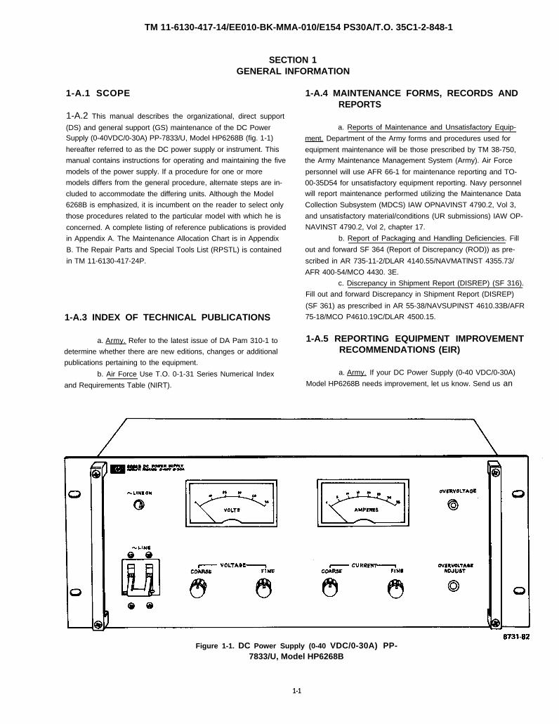
(DS) and general support (GS) maintenance of the DC PowerSupply (0-40VDC/0-30A) PP-7833/U, Model HP6268B (fig. 1-1)
hereafter referred to as the DC power supply or instrument. This
manual contains instructions for operating and maintaining the five
models of the power supply. If a procedure for one or more
models differs from the general procedure, alternate steps are in-
cluded to accommodate the differing units. Although the Model
6268B is emphasized, it is incumbent on the reader to select only
those procedures related to the particular model with which he is
concerned. A complete listing of reference publications is provided
in Appendix A. The Maintenance Allocation Chart is in Appendix
B. The Repair Parts and Special Tools List (RPSTL) is contained
in TM 11-6130-417-24P.
1-A.3 INDEX OF TECHNICAL PUBLICATIONS
a. Army. Refer to the latest issue of DA Pam 310-1 to
determine whether there are new editions, changes or additional
publications pertaining to the equipment.
b. Air Force Use T.O. 0-1-31 Series Numerical Index
and Requirements Table (NIRT).
1-A.4 MAINTENANCE FORMS, RECORDS ANDREPORTS
a. Reports of Maintenance and Unsatisfactory Equip-
ment. Department of the Army forms and procedures used for
equipment maintenance will be those prescribed by TM 38-750,
the Army Maintenance Management System (Army). Air Force
personnel will use AFR 66-1 for maintenance reporting and TO-
00-35D54 for unsatisfactory equipment reporting. Navy personnel
will report maintenance performed utilizing the Maintenance Data
Collection Subsystem (MDCS) IAW OPNAVINST 4790.2, Vol 3,
and unsatisfactory material/conditions (UR submissions) IAW OP-
NAVINST 4790.2, Vol 2, chapter 17.
b. Report of Packaging and Handling Deficiencies. Fill
out and forward SF 364 (Report of Discrepancy (ROD)) as pre-
scribed in AR 735-11-2/DLAR 4140.55/NAVMATlNST 4355.73/
AFR 400-54/MCO 4430. 3E.
c. Discrepancy in Shipment Report (DISREP) (SF 316).
Fill out and forward Discrepancy in Shipment Report (DISREP)
(SF 361) as prescribed in AR 55-38/NAVSUPINST 4610.33B/AFR
75-18/MCO P4610.19C/DLAR 4500.15.
1-A.5 REPORTING EQUIPMENT IMPROVEMENTRECOMMENDATIONS (EIR)
a. Army. If your DC Power Supply (0-40 VDC/0-30A)
Model HP6268B needs improvement, let us know. Send us an
Figure 1-1. DC Power Supply (0-40 VDC/0-30A) PP-7833/U, Model HP6268B
1-1
TM 11-6130-417-14/EE010-BK-MMA-010/E154 PS30A/T.O. 35C1-2-848-1
EIR. You, the user, are the only one who can tell us what youdon’t like about your equipment. Let us know why you don’t likethe design. Put it onan SF 368 (Quality Deficiency Report). Mail it to Commander, USArmy Communications-Electronics Command and Fort Monmouth,ATTN: DRSEL-ME-MP, Fort Monmouth, New Jersey 07703. We’llsend you a reply.
b. Air Force. Air Force personnel are encouraged tosubmit ElR’s in accordance with AFM 900-4.
c. Navy. Navy personnel are encouraged to submitElR’s through their local Beneficial Suggestion Program.
1-A.6 ADMINISTRATIVE STORAGE
1-A.7 Administrative Storage of equipment issued to and usedby Army activities will have preventive maintenance performed inaccordance with the PMCS procedures before storing. When re-moving the equipment from administrative storage, an operationalcheck should be performed as per paragraph 3-2 to assure opera-
tional readiness. Disassembly and repacking of equipment forshipment or limited storage are covered in TM-749-90-1.
1-A.8 DESTRUCTION OF ARMY ELECTRONICSMATERIEL
1-A.9 Destruction of Army electronics materiel to prevent en-emy use shall be in accordance with TM 750-244-2.
1-A.10 PURPOSE AND USE
1-A11 The supply is used as a power source to provide regu-lated zero to 40 Vdc for test procedures for the Central MessageSwitch and Automatic AN/TYC-39(V)1 and Circuit Switch AN/TTC-39(V)1, V2 and V3. The output of the supply can be varied fromzero to fully rated voltage or current via manual controls or by re-mote programming.
1-2
TM 11-6130-417-14/EE010-BK-MMA-010/E154 PS30A/T.O. 35C1-2-848-1
1-1 DESCRIPTION
1-2 The five constant-voltage/constant current powersupply models included in this manual use a transistor
series-regulator combined with a triac preregulator for highefficiency, excellent regulation, and low ripple and noise.
These supplies are packaged in 7-inch high full-rack-widthcabinets that are suitable for either bench or relay rack
operation.
1-3 The outputs of these supplies can be varied fromzero to full rated voltage or current by setting coarse andfine voltage and current controls on the front panel or they
can be programmed remotely by resistance or voltage inputs
to rear panel terminals. When the voltage controls are usedto establish a constant output voltage, the current controlsestablish a current limit that can protect the load from over-current. When the current controls are used to establish aconstant output current, the voltage controls establish avoltage limit that can protect the load from excessive
voltage. The crossover from constant-voltage to constant-current operation, or vice versa, occurs automatically whenthe load current reaches the value established by the currentcontrols or the voltage reaches the value established by thevoltage controls. The output voltage and current can both
be monitored continuously on front panel meters.
1-4 Output loads are further protected by a built-infast-acting overvoltage protection crowbar circuit that
automatically shorts the supply’s output terminals if apreset voltage limit is exceeded. A front panel control sets
the voltage at which the crowbar trips and can be adjustedfrom approximately 10% to 110% of the supply’s maximum
rated voltage. When several supplies are installed in the
same system, whether in series, parallel, or independently,their crowbar circuits can be interconnected so that all will
trip simultaneously whenever any one of them does.
1-5 These power supplies are forced air cooled.
1-6 The ac input connections to these supplies are made
at rear panel terminals. All dc output, remote sensing, andremote programming connections are also made at rear
panel terminals. Either the positive or negative outputterminal of a supply may be grounded or the supply’s
output may be floated at up to 300 volts above ground.
1-7 Remote programming, remote sensing, and several
methods of operating supplies in combination of two or
three are made possible by rear panel terminals that allow
access to control points within the regulator circuits, Thesecapabilities are described below.
a. Remote Programming. The power supply’s outputvoltage or current (or both) can be controlled from a remote
location by varying a resistance or a voltage input signal to
the supply’s voltage or current regulator circuit.
b. Remote Sensing. Connecting the voltage regulator’sfeedback circuit to the load terminals rather than to thesupply’s output terminals prevents the voltage drop in theload leads from impairing voltage regulation at the load
when operating in the constant voltage mode. A separate
pair of sensing leads which carry no load current extendthe feedback loop to the load terminals.
c. Auto-Parallel Operation. Two or three similar
supplies connected in parallel can be made to share loadsequally and can be controlled by the voltage and current
controls (or remote programming terminals) of one of the
supplies designated the master if they are connected forauto-parallel operation. Normally, only supplies havingthe same model number are connected in auto-parallel, but
auto-parallel operation can be used with any of the suppliescovered by this manual that have equal current capabilities.
d. Auto-Series Operation. Two or three supplies canbe connected in series and have their outputs simultaneouslycontrolled by the voltage and current controls (or remoteprogramming terminals) of one of the supplies designated
the master. The voltage contributed by each slave is main-tained in a constant ratio to that of the master. Theseratios can be set as desired. Auto-series operation provideshigher output voltages in constant voltage operation andgreater voltage compliance in constant current operation.Any HP supply that offers auto-series operation can serve
as a slave supply; the master supply does not have to be anauto-series model.
e. Auto-Tracking Operation. Auto-tracking is similar
to auto-series operation except that two or three supplies
share a common negative output bus and are interconnectedso that the output voltage of each slave supply is maintained
at some constant fraction of that of the master supply. Allof the supplies are controlled through the master supply,and each supply feeds a separate load.
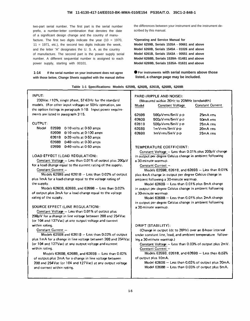
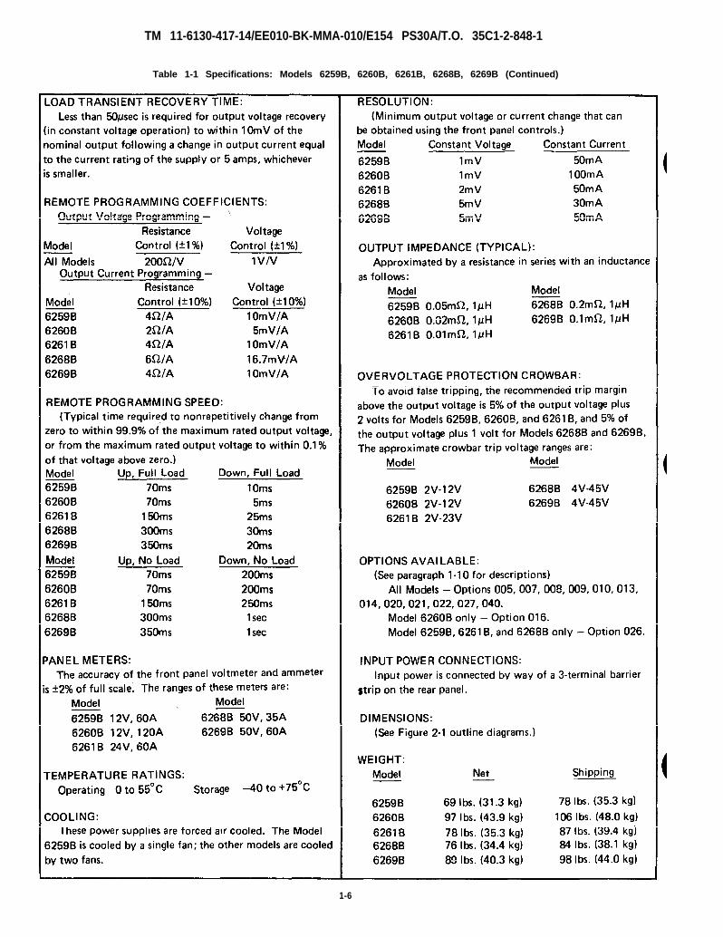
1-8 SPECIFICATIONS
1-9 Detailed specifications for these power supplies
are given in Table 1-1.
1-3
TM 11-6130-417-14/EE010-BK-MMA-010/E154 PS30A/T.O. 35C1-2-848-1
1-10 OPTIONS Option No. Description
Adjustable Voltage Programming: Two1-11 Options are customer-requested factory modifica- 020tions of a standard instrument. The following options are
available for the instruments covered by this manual. Wherenecessary, detailed coverage of the options is included
throughout the manual.
screwdriver-adjustable controls accessible
through holes in the rear panel allow thevoltage programming coefficient and zerooutput voltage to be adjusted conveniently
to an accuracy of 0.1%.
Option No. DescriptionAdjustable Current Programming: Two
screwdriver-adjustable controls accessiblethrough holes in the rear panel allow thecurrent programming coefficient and zero
output current to be adjusted conveniently
to an accuracy of 0.1%.
021
005 Realignment for 50Hz Operation: Standardinstruments are designed for 57 to 63Hz
operation. For 50Hz operation, a resistorin the preregulator control circuit is changed
and the preregulator is realigned.
007 Ten-Turn Output Voltage Control: A ten-
turn control replaces the coarse voltage con-
trol for improved resolution in setting the
output voltage.
022 Adjustable Voltage and Current Programming:
This option includes Options 020 and 021
in the same instrument.
026 Rewiring for 115Vac ±10% Single-Phase
Input (Models 6259B, 6261B, and 6268B only):
This factory modification replaces the circuit008 Ten-Turn Output Current Control: A ten-
turn control replaces the coarse currentcontrol for improved resolution in setting
the output current.
breaker (except in the Model 6259B), adds
a resistor to the A2 assembly, and reconnects
the power transformer, bias transformer,preregulator choke, and fans for 115Vac
operation.
009 Ten-Turn Output Voltage and Current
Controls: This option includes Options007 and 008 in the same instrument.
027 Rewiring for 208Vac ±10% Single-Phase
Input: This factory modification reconnects010 Chassis Slides: Factory installed slides
the power and bias transformers for 208Vacpermit convenient access to the interior ofa rack mounted supply for maintenance. operation.
013 040Three-Digit Graduated Decadial Voltage
Control: To improve mechanical stability
and permit accurate resetting of the output
Interfacing for Multiprogrammer Operation:
This factory modification prepares standard
power supplies for resistance programmingby the 6940B Multiprogrammer or the6941B Multiprogrammer Extender. Operationwith either of these instruments requires thatthe power supply be subjected to a specialcalibration and a protection checkout. The
special calibration insures that the powersupply can be accurately set to zero and to
the maximum rated output voltage or currentwhen programmed by the multiprogrammer.The protection checkout insures that the
power supply will not be damaged by therapid repetitive programming possible withthe multiprogrammer. This option includesOption 022.
voltage, Option 013 replaces the coarsevoltage control with a ten-turn controlequipped with a 3-digit turns-counting dial.
014 Three-Digit Graduated Decadial Current
Control: To improve mechanical stability
and permit accurate resetting of the outputcurrent, Option 014 replaces the coarse
current control with a ten-turn controlequipped with a 3-digit turns-counting dial.
016 Rewiring for 115Vac ±10% Single-PhaseInput (Model 6260B only): This factory
modification replaces the circuit breaker
and power transformer, adds a resistor to theA2 assembly, and reconnects the bias trans-former, preregulator choke, and fans for
115Vac operation.
1-12 lNSTRUMENT/MANUAL IDENTIFICATION
1-13 Hewlett-Packard power supplies are identified by a
1-4
TM 11-6130-417-14/EE010-BK-MMA-010/E154 PS30A/T.O. 35C1-2-848-1
two-part serial number. The first part is the serial numberprefix, a number-letter combination that denotes the dateof a significant design change and the country of manu-
facture. The first two digits indicate the year (10 = 1970,11 = 1971, etc.), the second two digits indicate the week,
and the letter “A” designates the U. S. A. as the countryof manufacture. The second part is the power supply serialnumber. A different sequential number is assigned to each
power supply, starting with 00101.
the differences between your instrument and the instrument de-scribed by this manual.
*Operating and Service Manual forModel 6259B, Serials 1535A - 00661 and aboveModel 6260B, Serials 1545A - 01026 and aboveModel 6261B, Serials 1543A - 00551 and aboveModel 6268B, Serials 1539A- 01481 and aboveModel 6269B, Serials 1535A- 01631 and above
1-14 If the serial number on your instrument does not agree ● For instruments with serial numbers above thosewith those below, Change Sheets supplied with the manual define listed, a change page may be included.
Table 1-1 Specifications: Models 6259B, 6260B, 6261B, 6268B, 6269B
1-5
2-1
TM 11-6130-417-14/EE010-BK-MMA-010/E154 PS30A/T.O. 35C1-2-848-1
Table 1-1 Specifications: Models 6259B, 6260B, 6261B, 6268B, 6269B (Continued)
1-6
TM 11-6130-417-14/EE010-BK-MMA-010/E154 PS30A/T.O. 35C1-2-848-1
1-15 ORDERING ADDITIONAL MANUALS
1-16 One manual is shipped with each power supply. Addi-
installed.
tional manuals may be obtained from regular publication distribu- ACCESSORYtion channels.
1-17 EQUIPMENT SUPPLIED
1-18 The equipment supplied with each Model HP6266B
Regulated DC Power Supply (0-40 VDC/0-30A) is an AC cable
strain relief assembly HP Part No. 5060-2744. This item is used to
reduce the possible hazard of an accidental disconnecting of the
user-supplied ac power cable. The enclosed strain relief assembly
with related hardware must be installed when the power supply is
1-19
1-20
EQUIPMENT AVAILABLE
The standard model of the 0-40 Vdc Power Supply is or-
dinarily wired for 230 Vac input power. However, with respect to
the HP6268B model (to which this manual is chiefly dedicated),
the standard model has already been adapted to 115 Vac input
power by: replacing the circuit breaker, by adding a resistor, and
by rearranging certain jumpers. In summary, two pieces of acces-
sory equipment have already been added to the standard model to
establish this HP6268B model with the 026 option.
1-7/(1-8 blank)

TM 11-6130-417-14/EE010-BK-MMA-010/E154 PS30A/T.O. 35C1-2-848-1
SECTION IIINSTALLATION
2-1 INITIAL INSPECTION2-2 Before shipment, this instrument was inspected andfound to be free of mechanical and electrical defects. As soon asthe instrument is unpacked, inspect for any damage that may haveoccurred in transit. Save all packing materials until the inspectionis cornpleted. If damage is found, take action immediately.
2-3 Mechanical Check2-4 This check should confirm that there are nobroken knobs or connectors, that the cabinet and panelsurfaces are free of dents and scratches, and that themeters are not scratched or cracked.
2-5 Electrical Check2-6 The instrument should be checked against itselectrical specifications. Section V includes an “in-cabinet”performance check to verify proper instrument operation.
2-7 INSTALLATION DATA2-8 The instrument is shipped ready for permanent rack in-stallation or bench operation. It is necessary only to connect auser-supplied power cord to the power supply, install the ACpower cable strain relief assembly and connect power cord tosource of supply. See paragraph 2-34 for procedures.
2-9 Location and Cooling2-10 These instruments are fan-cooled and must beinstalled with sufficient space for cooling air to reach theirsides. These power supplies should be used in an areawhere the ambient temperature does not exceed 55°C.
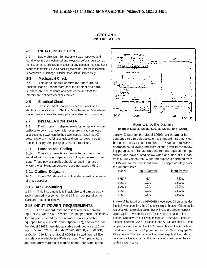
2-11 Outline Diagram2-12 Figure 2-1 shows the outline shape and dimensionsof these supplies.
2-13 Rack Mounting2-14 This instrument is full rack size and can be easilyrack mounted in a conventional 19-inch rack panel usingstandard mounting screws.
2-15 INPUT POWER REQUIREMENTS2-16 The standard instrument is wired for a nominalinput of 230Vac 57-63Hz when it is shipped from the factoryThe supplies covered by this manual are also availableequipped for a 208-volt input (Option 027), and except forthe Model 6269B, are also available equipped for a 115-voltinput (Option 026 for Models 6259B, 6261B, and 6268B,or Option 016 for the Model 6260B). In addition, all fivemodels are available in a 50Hz version. The input voltageand frequency required is marked on the rear panel of the
Figure 2-1. Outline Diagrams
(Models 6259B, 6260B, 6261B, 6268B, and 6269B)
supply. Except for the Model 6269B, which cannot beconverted to 115-volt operation, a standard instrument canbe converted by the user to 208 or 115-volt and to 50Hzoperation by following the instructions given in the follow-ing paragraphs. The standard instrument requires the inputcurrent and power listed below when operated at full loadfrom a 230-volt source. When the supply is operated froma 115-volt source, the input current is approximately twicethe amount listed.
Model Input Current Input Power
6259B 6A 850W6260B 12A 1600W6261B 12A 1500W6268B 12A 1600W6269B 18A 2500W
In view of the fact that the HP6268B model uses 24 amperes dur-ing 115-Vac operation, the 20-ampere circuit breaker CB1 must bereplaced with a circuit breaker that will handle a greater currentvalue. Option 026 specifies that, for 115-Vac operation, circuitbreaker CB1 have the following rating: 30A, 250 Vac, 2-pole. Inaddition, a resistor A2R3 is added to the A2 RFI assembly. Somejumpers are rerouted on the A2 RFI assembly, on the A3T2 biastransformer, and on the T1 power transformer. See paragraph 2-25 for details. The rear panel of the power supply at hand shouldbe examined to ensure that the unit is wired correctly for the in-tended power source.
2-1
TM 11-6130-417-14/EE010-BK-MMA-010/E154 PS30A/T.O. 35C1-2-848-1
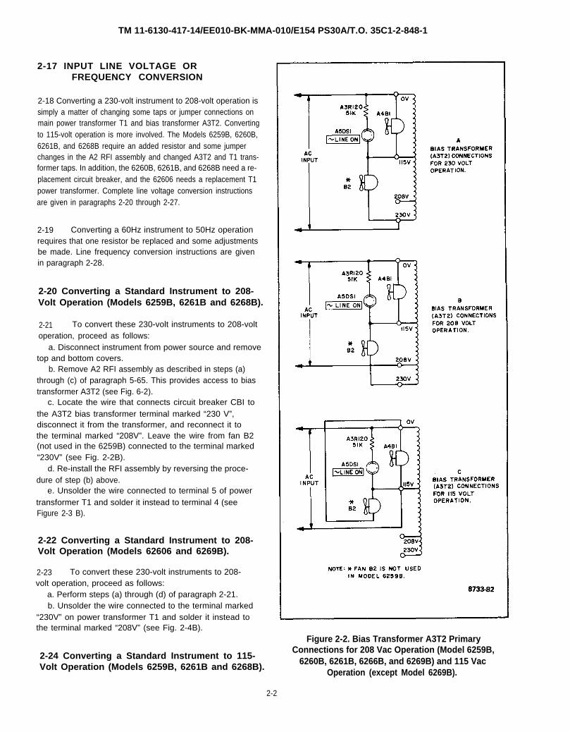
2-17 INPUT LINE VOLTAGE ORFREQUENCY CONVERSION
2-18 Converting a 230-volt instrument to 208-volt operation issimply a matter of changing some taps or jumper connections onmain power transformer T1 and bias transformer A3T2. Convertingto 115-volt operation is more involved. The Models 6259B, 6260B,6261B, and 6268B require an added resistor and some jumperchanges in the A2 RFI assembly and changed A3T2 and T1 trans-former taps. In addition, the 6260B, 6261B, and 6268B need a re-placement circuit breaker, and the 62606 needs a replacement T1power transformer. Complete line voltage conversion instructionsare given in paragraphs 2-20 through 2-27.
2-19 Converting a 60Hz instrument to 50Hz operationrequires that one resistor be replaced and some adjustmentsbe made. Line frequency conversion instructions are givenin paragraph 2-28.
2-20 Converting a Standard Instrument to 208-Volt Operation (Models 6259B, 6261B and 6268B).
2-21 To convert these 230-volt instruments to 208-voltoperation, proceed as follows:
a. Disconnect instrument from power source and removetop and bottom covers.
b. Remove A2 RFI assembly as described in steps (a)through (c) of paragraph 5-65. This provides access to biastransformer A3T2 (see Fig. 6-2).
c. Locate the wire that connects circuit breaker CBI tothe A3T2 bias transformer terminal marked “230 V”,disconnect it from the transformer, and reconnect it tothe terminal marked “208V”. Leave the wire from fan B2(not used in the 6259B) connected to the terminal marked“230V” (see Fig. 2-2B).
d. Re-install the RFI assembly by reversing the proce-dure of step (b) above.
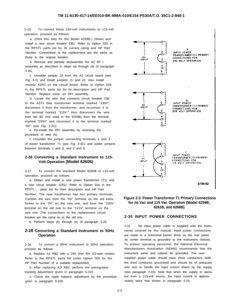
e. Unsolder the wire connected to terminal 5 of powertransformer T1 and solder it instead to terminal 4 (seeFigure 2-3 B).
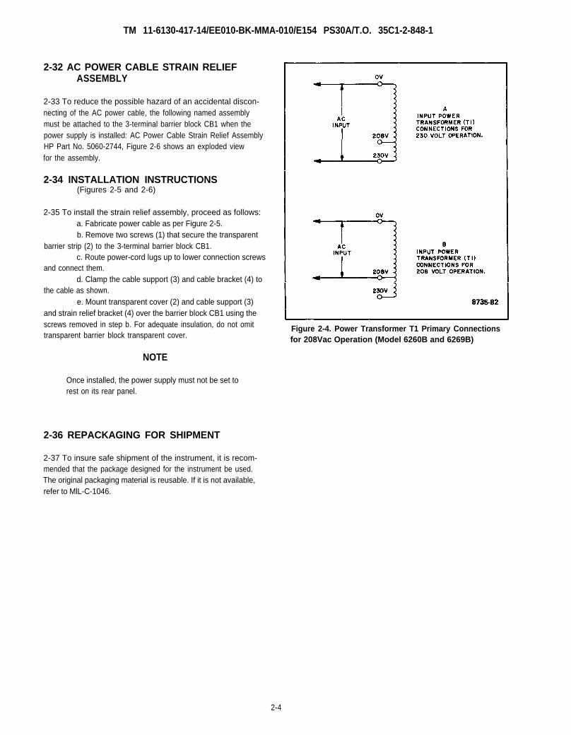
2-22 Converting a Standard Instrument to 208-Volt Operation (Models 62606 and 6269B).
2-23 To convert these 230-volt instruments to 208-volt operation, proceed as follows:
a. Perform steps (a) through (d) of paragraph 2-21.b. Unsolder the wire connected to the terminal marked
“230V” on power transformer T1 and solder it instead tothe terminal marked “208V” (see Fig. 2-4B).
2-24 Converting a Standard Instrument to 115-Volt Operation (Models 6259B, 6261B and 6268B).
Figure 2-2. Bias Transformer A3T2 PrimaryConnections for 208 Vac Operation (Model 6259B,
6260B, 6261B, 6266B, and 6269B) and 115 VacOperation (except Model 6269B).
2-2
TM 11-6130-417-14/EE010-BK-MMA-010/E154 PS30A/T.O. 35C1-2-848-1
2-25 To convert these 230-volt instruments to 115-volt
operation, proceed as follows:
a. (Omit this step for the Model 6259B.) Obtain and
install a new circuit breaker CB1. Refer to Option 026 in
the RPSTL parts list for its current rating and HP Part
Number. Connections to the replacement are the same as
those to the original breaker.
b. Remove and partially disassemble the A2 RF I
assembly as described in steps (a) through (d) of paragraph
5-65.
c. Unsolder jumper J3 from the A2 circuit board (see
Fig. 6-1) and install jumpers J1 and J2. Also install
resistor A2R3 on the circuit board. Refer to Option 026
in the RPSTL parts list for its description and HP Part
Number. Replace cover on RFI assembly.
d. Locate the wire that connects circuit breaker CBI
to the A3T2 bias transformer terminal marked “230V”,
disconnect it from the transformer, and reconnect it to
the terminal marked “115V.” Also disconnect the wire
from fan B2 (not used in the 6259B) from the terminal
marked “230V” and reconnect it to the terminal marked
“0V” (see Fig. 2-2C).e. Re-install the RFI assembly by reversing the
procedure of step (b).
f. Unsolder the jumper connecting terminals 2 and 3
of power transformer T1 (see Fig. 2-3C) and solder jumpers
between terminals 1 and 3, and 2 and 5.
2-26 Converting a Standard Instrument to 115-Volt Operation (Model 62606)
2-27 To convert the standard Model 6260B to 115-volt
operation, proceed as follows:
a. Obtain and install a new power transformer (T1) and
a new circuit breaker (CB1). Refer to Option 016 in theRPSTL parts list for their description and HP Part
Number. The new transformer has two primary terminals.
Transfer the wire from the “0V” terminal on the old trans-
former to the “0V” on the new one, and from the “230V”
terminal on the old one to the “115V” terminal on the
new one. The connections to the replacement circuit
breaker are the same as to the old one.
b. Perform steps (b) through (e) of paragraph 2-25.
2-28 Converting a Standard Instrument to 50HzOperation
2-29 To convert a 60Hz instrument to 50Hz operation,
proceed as follows:
a. Replace A1 R82 with a 240 ohm 5% 1/2-watt resistor.
Refer to the RPSTL parts list under Option 005 for the
HP Part Number of a suitable replacement.
b. After replacing A2l R82, perform the preregulator
tracking adjustment given in paragraph 5-102.
c. Check the ripple balance adjustment by the procedure
given in paragraph 5-100.
Figure 2-3. Power Transformer T1 Primary Connectionsfor 208 Vac and 115 Vac Operation (Model 6259B,
6261B, and 6268B)
2-30 INPUT POWER CONNECTIONS
2-31 No input power cable is supplied with the instru-
ments covered by this manual. Input power connections
are made to a 3-terminal barrier block on the rear panel.
Its center terminal is grounded to the instrument chassis.
To protect operating personnel, the National Electrical
Manufacturers Association (NEMA) recommends that the
instrument panel and cabinet be grounded. The user-
supplied power cable should have three conductors (with
the third conductor grounded) and should be of adequate
wire size to handle the input current drawn by the supply
(see paragraph 2-15). Note that when the supply is opera-ted from a 115-volt source, the input current is approxi-
mately twice that shown in paragraph 2-15.
2-3
TM 11-6130-417-14/EE010-BK-MMA-010/E154 PS30A/T.O. 35C1-2-848-1
2-32 AC POWER CABLE STRAIN RELIEFASSEMBLY
2-33 To reduce the possible hazard of an accidental discon-necting of the AC power cable, the following named assemblymust be attached to the 3-terminal barrier block CB1 when thepower supply is installed: AC Power Cable Strain Relief AssemblyHP Part No. 5060-2744, Figure 2-6 shows an exploded viewfor the assembly.
2-34 INSTALLATION INSTRUCTIONS(Figures 2-5 and 2-6)
2-35 To install the strain relief assembly, proceed as follows:a. Fabricate power cable as per Figure 2-5.b. Remove two screws (1) that secure the transparent
barrier strip (2) to the 3-terminal barrier block CB1.c. Route power-cord lugs up to lower connection screws
and connect them.d. Clamp the cable support (3) and cable bracket (4) to
the cable as shown.e. Mount transparent cover (2) and cable support (3)
and strain relief bracket (4) over the barrier block CB1 using thescrews removed in step b. For adequate insulation, do not omittransparent barrier block transparent cover.
NOTE
Once installed, the power supply must not be set torest on its rear panel.
2-36 REPACKAGING FOR SHIPMENT
2-37 To insure safe shipment of the instrument, it is recom-mended that the package designed for the instrument be used.The original packaging material is reusable. If it is not available,refer to MlL-C-1046.
Figure 2-4. Power Transformer T1 Primary Connectionsfor 208Vac Operation (Model 6260B and 6269B)
2-4
TM 11-6130-417-14/EE010-BK-MMA-010/E154 PS30A/T.O. 35C1-2-848-1
Figure 2-5. Power Cable
2-5
TM 11-6130-417-14
2-6
Figure 2-6.
TM 11-6130-417-14/EE010-BK-MMA-010/E154 PS30A/T.O. 35C1-2-848-1
SECTION IIIOPERATING INSTRUCTIONS
Figure 3-1. Front Panel Controls and Indicators
3-1 TURN-ON CHECKOUT PROCEDURE
3-2 The following steps describe the use of the front
panel controls and indicators illustrated in Figure 3-1 and
serve as a brief check that the supply is operational. This
checkout procedure or the more detailed performance
test of paragraph 5-5 should be followed when the instru-
ment is received and before it is connected to any load
equipment. Proceed to the more detailed test and trouble-
shooting procedures in Section V if any difficulties are
encountered.
a. Turn CURRENT controls and OVERVOLTAGE
ADJUST potentiometer fully clockwise and check
that rear panel straps are connected as shown in Figure 3-2,
but do not connect load RL.
b. Connect ac power of the appropriate voltage and
frequency to the rear panel ac and acc terminals. The
supply’s input rating is identified on its rear panel.
WARNING
Do not interchange the ac and acc input lines;
connect the ac input terminal to the hot side
and the acc input terminal to the grounded
side of the ac line. Do not fail to connect the
input ground terminal ( ) securely to an
external earth ground.
c. Set LINE switch or circuit breaker ON and
observe that pilot lamp lights.
d. Adjust COARSE and FINE VOLTAGE controls
for desired indication on voltmeter
e. Ensure that overvoltage crowbar circuit is operational
by slowly turning OVERVOLTAGE ADJUST control
counterclockwise with a screwdriver until OVERVOLTAGE
lamp lights and voltmeter indication drops to zero
volts.
3-1
TM 11-6130-417-14/EE010-BK-MMA-010/E154 PS30A/T.O. 35C1-2-848-1
f. Reset crowbar by returning OVERVOLTAGE
ADJUST control to its maximum clockwise position andturning off the supply. On turning the supply back on,the voltage should be the same value as was set in step (d).
g. To check the constant current circuit, first turn offthe supply, connect a short across the output bus bars(see Figure 3-2), and turn it back on.
h. Adjust COARSE and FINE CURRENT controls until ammeter indicates desired output current orcurrent limit. (The VOLTAGE controls must be set fora greater-than-zero output to obtain the output currentprogrammed.)
i. Turn off the supply, remove the short from its out-put, and read the remainder of these operating instructionsbefore connecting the supply to an actual load.
3-3 OPERATING MODES
3-4 This power supply is designed so that its mode of oper-ation can be selected by making strapping connections betweenterminals on its rear panel. The following paragraphs first describenormal operation using the normal strapping pattern as it is con-nected at the factory.
3-5 Later paragraphs cover some optional operating modesincluding remote voltage sensing, remote programming, and somemethods of operating these power supplies in combinations of twoor three.
3-6 NORMAL OPERATING MODE
3-7 This power supply was shipped with the proper rearpanel strapping connections made for constant-voltage/constant-current operation with local sensing and local programming. Thisstrapping pattern is illustrated in Figure 3-2. In the constant-volt-age mode, the power supply acts to maintain its output voltageconstant in spite of changes in load, line, temperature, etc. Thus,for a change in load resistance, the output voltage of this moderemains constant while the output current changes by whateveramount necessary to accomplish this. In the constant-currentmode, the power supply acts to maintain its output current con-stant in spite of changes in load, line, temperature, etc. Thus, for achange in load resistance, the output current remains constantwhile the output voltage changes by whatever amount necessaryto accomplish this. By means of the front panel voltage and cur-rent controls, the operator selects either a constant-voltage or aconstant-current output. Whether the supply functions in the con-stant-voltage or the constant-current mode depends on the set-tings of the voltage and current controls and on the resistance ofthe output load. For values of load resistance greater than a criti-cal crossover value equal to the voltage setting divided by the cur-rent setting, the supply operates in the constant-voltage mode.With a load resistance smaller than this critical value, it operatesin the constant-current mode. The transition occurs automatically;
no switches need to be operated or connections changed.3-2
Figure 3-2. Normal Strapping Pattern
3-8 Constant Voltage Operation
3-9 To adjust the supply for constant voltage operation:a. Turn on supply and, with output terminals open,
adjust the VOLTAGE controls for the desired output
voltage. Then turn power off.
b. Connect a short across the rear panel output termimals,
restore power, and adjust the CURRENT controls for the
desired maximum output current. Then remove the short.
If a load change causes this current limit to be exceeded,
the supply automatically crosses over to constant current
operation at this preset current limit and the output voltagedrops proportionately. In setting the current limit, makean adequate allowance for high peak currents that couldcause unwanted crossover. (Refer to paragraph 3-77.)
3-10 Constant Current Operation
3-11 To adjust the supply for constant current operation:
a. Connect a short across the rear output terminals, turnthe power on, and adjust the CURRENT controls for thedesired output current.
b. Open the output terminals and adjust the VOLTAGE
controls for the desired maximum output voltage. If a
load change causes this voltage limit to be exceeded, the
supply automatically crosses over to constant voltage opera-
tion at this preset voltage limit and the output current drops
proportionately. In setting the voltage limit, make an
adequate allowance for high peak voltages that could cause
unwanted crossover. (Refer to paragraph 3-77.)
3-12 Overvoltage Trip Point Adjustment
3-13 The crowbar trip voltage is adjusted by using the screw-
driver control on the front panel. The approximate trip voltage
ranges are listed in Table 1-1. When the crowbar trips, an SCR
shorts the output and the amber OVER-VOLTAGE indicator on the
front panel lights. Rotating the control clockwise sets the trip volt-
age higher. (It is set to maximum at the factory.) Paragraph 5-104
contains the procedure for adjusting the trip voltage, while para-
graph 5-108 contains instructions for completely disabling the
crowbar, if this is desired.
TM 11-6130-417-14/EE010-BK-MMA-010/E154 PS30A/T.O. 35C1-2-848-1
3-14 When adjusting the crowbar trip point, the
possibility of false tripping must be considered. If the trip
voltage is set too close to the supply’s operating voltage,
a transient in the output would falsely trip the crowbar.
For this reason it is recommended that the crowbar be set
higher than the output voltage by 5% of the output voltage
plus 2 volts for the Models 6259B, 6260B, or 6261B, or
5% of the output voltage plus one volt for the Models 6268B
or 6269B. If an occasional tripping of the crowbar can be
tolerated as a load is being disconnected, the crowbar trip
point can be set much closer to the operating voltage of
the supply.
3-15 Connecting The Load
3-16 To satisfy the requirements of safety, the wires to
the load should be at least heavy enough not to overheat
while carrying the power supply current that would flow if
the load were shorted. Generally, heavier wire than this isrequired to obtain good regulation at the load. If the load
regulation is critical, use remote voltage sensing. (Refer to
paragraph 3-27.)
3-17 If multiple loads are connected to one supply,
each load should be connected to the supply’s output
terminals using separate pairs of connecting wires. This
minimizes mutual coupling effects between loads and takes
full advantage of the supply’s low output impedance. Each
pair of connecting wires should be as short as possible and
twisted or shielded to reduce noise pickup.
3-18 If load considerations require the use of output
distribution terminals that are located remotely from the
supply, then the power supply output terminals should
be connected to the remote distribution terminals by a
pair of twisted or shielded wires and each load should be
separately connected to the remote distribution terminals.
Remote voltage sensing would be required under these
circumstances. (Refer to paragraph 3-27.)
3-19 Either positive or negative voltages can be obtained
from this supply by grounding one of the output terminals
or one end of the load. Always use two wires to connect
the load to the supply regardless of where or how the
system is grounded. Never ground the system at more than
one point. This supply can be operated up to 300 volts
above ground if neither output terminal is grounded.
3-20 Operation With No Load
3-21 When the supply is operated without a load, its
down-programming speed is considerably slower than when
its output is loaded. This slower programming speed is
evident whether the VOLTAGE controls are turned fully
counterclockwise or an external voltage programming input
signal is decreased. When the crowbar is activated during
no-load operation, the supply’s output falls rapidly to about
two volts and then decreases more slowly towards zero.
The actual time required for the output to fall from two
volts to zero varies from several seconds to several minutes,
depending on the output rating of the supply.
3-22 Operation Beyond Rated Output
3-23 The supply may be able to provide voltages and
currents greater than its rated maximum outputs. Operation
can extend into the shaded areas on the meter face without
damage to the supply, but performance cannot be guaranteed
to meet all specifications.
3-24 OPTIONAL OPERATING MODES
3-25 The optional operating modes discussed in the
following paragraphs include:
a. Remote voltage sensing
b. Remote programming
c. Auto-Parallel operation
d. Auto-Series operation
e. Auto-Tracking operation
Special operating instructions for instruments equipped with Option
040 to permit their interfacing with a Model 6940B Multiprogram-
mer or a 6941B Multiprogrammer Extender are not included but
can be found in the manual covering the programmable resistance
cards that are necessary to complete the interface. Special cali-
bration instructions for power supplies equipped with Option 040
are included in Section V of this manual. in the following para-
graphs, all resistors are located on the printed circuit board A1 un-
less otherwise noted.
3-26 By changing its rear panel strapping pattern
according to the instructions which follow, any of the
supplies covered by this manual can be operated in any
of the modes listed above.
WARNING
Disconnect input ac power before changing any
rear panel connections and make certain all wires
and straps are properly connected and terminal
strip screws are securely tightened before
reapplying power.
3-27 Remote Voltage Sensing
3-28 Because of the unavoidable voltage drop developed in
the load leads, the normal strapping pattern shown in Figure 3-2
will not provide the best possible voltage regulation at the load. If,
for example, one were to use 4-gauge wire to connect a load that
3-3
TM 11-6130-417-14/EE010-BK-MMA-010/E154 PS30A/T.O. 35C1-2-848-1
is located only 5 feet from a Model 6268B, 0-40V 0-30A supply,
the full-load regulation measured at the load would be about 75
millivolts as compared to the 4.2 millivolt regulation that could be
measured at the supply’s output terminals. Thus even relatively
short load leads can cause a considerable degradation of the sup-
ply’s performance. The remote sensing connections shown in Fig-
ure 3-3 improve the voltage regulation at the load by monitoring
the voltage there instead of at the supply’s output terminals. (The
advantages of remote sensing apply only during constant voltage
operation.)
3-29 As can be seen in Figure 3-3, remote sensing
involves removing the +S and -S jumpers from the output
terminals, connecting the load leads normally, and using
a separate pair of wires to connect the +S and -S sensing
terminals to the load. The following paragraphs discuss
some precautions that should be observed when making
a remote sensing installation.
NOTE
The +S jumper is the one that links the +S
terminal to the +OUT terminal when the
supply’s terminals are strapped for normal
operation as shown in Figure 3-2. The -S
jumper is the one that links the -S terminal
to the -OUT terminal.
3-30 The load leads should be of the heaviest practicable
wire gauge, at least heavy enough to limit the voltage drop
in each lead to 0.5 volt. This limitation is dictated by the
adverse effect that a greater load lead voltage drop has on
bias voltages within the supply when remote sensing is used.
Twisting the load leads may help to minimize noise pick-up.
While there are practical limitations on the distance that
can separate a power supply from its load when using remote
sensing, it isn’t possible to define these limits precisely due
to a variety of factors that are unique to each particular
installation.
Figure 3-3. Remote Sensing
3-31 Since the sensing leads carry only a few milliamps,
the wires used for sensing can be much lighter than the
load leads (22 AWG is generally adequate), but they should
be a shielded, twisted pair to minimize the pickup of
external noise. Any noise picked up on the sensing leads
will appear at the supply’s output. The shield should be
grounded at one end only and should not be used as one
of the sensing conductors. The sensing leads should be
connected as close to the load as possible.
3-32 The sensing leads are part of the supply’s program-
ming circuit, so they should be connected in such a way as
to make it unlikely that they might inadvertently become
open circuited. If the sensing leads were to open during
operation, the output voltage would tend to rise. Although
the increase would be limited by protective resistors R108
and R109, damage to the supply or to the load might occur
if the loss of sensing were accompanied by a load transient.
For this reason no switch, relay, or connector contacts
should be included in the remote sensing path.
— C A U T I O N —
When using remote voltage sensing, it is possible
to damage the supply by disconnecting a load
lead while the sensing lead is still connected and
the supply is energized. If a load lead becomes
disconnected, current flows through internal
protection resistors R108 and R109, the sensing
leads, and the load and may burn out the resistors.
Additional factors could compound the damage
caused by an opened load lead. If the output of
the supply is connected to an inductive load or a
battery *, or is connected in parallel with another
supply, then opening a load lead would allow
current from the external source to flow through
the sensing leads and damage the supply's input
circuits. If the crowbar fires, the damage could
even be greater.
For these reasons, if there is any risk of an opened
load circuit while remote sensing is used, 1/16-amp
fuses should be installed in both sensing leads.
Fuses in the sensing leads will not affect the
performance of the supply and should protect
against costly damage.
* Remote sensing is not recommended when charging or
discharging a battery. See paragraphs 3-87 and 3-91.
3-33 Another factor to be considered when making a remote
sensing installation is the inductance of the long load leads. Al-
though dc and low frequency performance are improved by remote
sensing, the higher inductance of longer leads does impair tran-
3-4
TM 11-6130-417-14/EE010-BK-MMA-010/E154 PS30A/T.O. 35C1-2-848-1
sient response and could affect the stability of the feedback loopseriously enough to cause oscillation. If remote sensing disturbsthe supply’s stability, the calibration technician should try thesetwo corrective measures:
a. Adjust the equalization control R47 until the oscilla-
tion stops. To achieve the best possible transient response for a
given remote sensing installation, measure the transient response
using the procedure given in paragraph 5-27 and adjust R47 while
observing the transient response waveforms.
b. If adjusting R47 does not eliminate the instability, it
may be beneficial to disconnect output capacitor A3C3 from the
circuit and connect a similar capacitor directly across the load. To
gain access to capacitor A3C3, the A2 RFI Assembly must first be
removed. Follow steps (a) through (c) of paragraph 5-65 to re-
move the A2 assembly. Then unsolder the heavy wire from the A3
circuit board that connects the positive terminal of A3C3 to the
positive output bus bar. (This heavy connecting point is identified
in Figure 6-2.)
NOTE
Do not unsolder the capacitor’s negative lead.
The negative lead to A3C3 carries collector
current for transistor A4Q101 and would
disable the power supply if disconnected.
Tape the free end of the disconnected wire, replace the A2
assembly, and replace the bottom cover of the supply. The
substitute capacitor should have approximately the same
capacitance, an equal or greater voltage rating, and good
high frequency characteristics. Connect it directly across
the load using the shortest possible leads. Readjust equali-zation control R47 as in step (a) above after installing the
substitute output capacitor.
3-34 Remote Programming
3-35 The output voltage or current of these power
supplies can be remotely controlled by connecting an
external resistor or applying an external voltage to rear
panel terminals. If resistance programming is used, a
variable resistor can control the output over its entire
range. Or, a variable resistor connected in series with a
fixed resistor can have its control restricted to a limited
portion of the output range. Alternately, a switch can be
used to select fixed values of programming resistance to
obtain a set of discrete voltages or currents. (The switch
must have make-before-break contacts to avoid producing
the output voltage transients that momentarily opening
the programming terminals would cause.) To maintain
the temperature and stability specifications of the supply,
programming resistors must be stable, low noise resistors
with a temperature coefficient of less than 30ppm per °C
and a power rating at least 30 times what they will actually
dissipate.
3-36 Both voltage and current outputs can also be
controlled through a voltage input. When voltage program-
ming the output voltage, the choice can be made between
using a connection that produces a unity gain relationship
between input and output (paragraph 3-41) or another
connection that produces variable voltage gains (paragraph
3-42). Similarly, the output current can be programmed
using a connection that produces a fixed gain (paragraph
3-47) or a variable gain (paragraph 3-48).
3-37 Connecting a supply for remote voltage or current
programming disables the corresponding front panel controls.
3-38 The following paragraphs discuss in greater detail the
methods of remotely programming the output voltage or current
using either a resistance or a voltage input. Whichever method is
used, the wires connecting the programming terminals of the sup-
ply to the remote programming device must be shielded to reduce
noise pickup. The outer shield of the cable should not be used as
a conductor but should be connected to ground at one end only.
All resistors are located on the main printed circuit board unless
otherwise noted.
3-39 Constant Voltage Output, Resistance Input. The
rear panel connections shown in Figure 3-4 allow the out-
put voltage to be varied by using an external resistor to
program the supply. The supply’s constant voltage program-
ming current determines its programming coefficient. In
the supplies covered by this manual, this programming
current is factory adjusted to within 1% of 5mA, resulting
in a programming coefficient of 200 ohms per volt. If a
greater programming accuracy is required, it can be obtained
either by changing resistor R3 as discussed in paragraph 5-86
or, if the instrument is equipped with Options 020 or 022,
by adjusting potentiometer R112 as discussed in paragraph
5-87. (See Figs. 6-1 through 6-8.)
3-40 With the programming terminals shorted (terminals
A2 to -S), the no-load output voltage of the supply should
be -15mV ±5mV. If a minimum output voltage is required
that is closer to zero than this, it can be obtained either
Figure 3-4. Resistance Programming of Output Voltage
3-5
TM 11-6130-417-14/EE010-BK-MMA-010/E154 PS30A/T.O. 35C1-2-848-1
by installing and adjusting R110 as discussed in paragraph
5-81 or, if the instrument is equipped with Option 020 or
022, by adjusting potentiometer R113 as discussed in
paragraph 5-83.
— C A U T I O N —
Do not allow programming terminals A2 or-S to become open circuited while resistanceprogramming the output voltage. If they dobecome open circuited, the supply’s outputvoltage tends to rise beyond its rated maximum.If the supply’s current controls and over-voltage crowbar trip point are properly adjusted,however, no damage to the power supply orload should result.
3-41 Constant Voltage Output, Voltage Input (UnityGain). The rear panel connections shown in Figure 3-5
allow the output voltage to be varied by using an externalvoltage source to program the supply. In this mode, the
output voltage varies in a 1 to 1 ratio with the program-
ming voltage. The load on the programming voltage source
is less than 20 microamperes. Impedance matching resistor
R X is required to maintain the temperature coefficient
and stability specifications of the supply. To adjust the
output voltage to exactly zero with a zero programming
voltage, follow the same instructions as are referred to in
paragraph 3-40. (See Figures 6-7 and 6-8.)
3-42 Constant Voltage Output, Voltage Input (VariableGain). In the remote programming arrangement shown
in Figure 3-6, the series combination of external voltage
source ES and reference resistor RR replaces the supply’s
internal voltage programming current source. As a result,
the voltage this external current source develops across
gain control Rp becomes the output voltage of the supply,
and the gain relationship between ES and the output volt-age equals the resistance ratio RP/RR.
3-43 When using this programming technique, select
a value for RR that is less than 10k ohms and that would
conduct at least 5 milliamps if connected across the
programming voltage source with its voltage at the maximum
value of input voltage to be used. Once the value for RR
is selected, multiply RR by the maximum voltage gain
desired to find Rp. (If desired, the power supply’s front
panel voltage controls can be used in place of external gain
control Rp by deleting the external gain control from the
circuit and strapping together terminals A1 and A2.)
3-44 The output voltage of the supply can be adjusted to ex-
actly zero with a zero programming voltage input either by install-ing and adjusting R111 as discussed in paragraph 5-82 or, if the
instrument is equipped with Option 020 or 022, by adjusting poten-
tiometer R112 as discussed in paragraph 5-63.
NOTEThe negative lead of the capacitor must not be un-
soldered. Removing this lead wiII cause the supply tostop functioning because the lead carries the collec-
tor current of transistor A4Q101.
3-45 Constant Current Output, Resistance Input. The
rear panel connections shown in Figure 3-7 allow the
output current to be varied by using an external resistor to
program the supply. The supply’s constant current program-
ming current, which is factory adjusted to 2.5mA ±10%,
determines the exact value of its programming coefficient.
The programming coefficients for the supplies included in
this manual are as follows:
Models 6259B 4 ohms/ampere
6260B 2 ohms/ampere
6261B 4 ohms/ampere
6268B 6 ohms/ampere
6269B 4 ohms/ampere
if the ±10% accuracy of these coefficients is not adequate,
Figure 3-5. Voltage Programming of Output Voltage Figure 3-6. Voltage Programming of Output Voltage(Unity Gain) (Variable Gain)
3-6
TM 11-6130-417-14/EE010-BK-MMA-010/E154 PS30A/T.O. 35C1-2-848-1
they may be adjusted either by changing resistor R30 as
discussed in paragraph 5-96 or, if the instrument is equipped
with Option 021 or 022, by adjusting potentiometer R116
as discussed in paragraph 5-97.
3-46 With zero ohms connected across the programming
terminals, the output current of the supply may be set to
exactly zero either by installing and adjusting R117 as
described in paragraph 5-91 or, if the instrument is equipped
with Option 021 or 022, by adjusting potentiometer R119
as discussed in paragraph 5-93.
— CAUTION —Do not allow programming terminals A4 or
A6 to become open-circuited while resistance
programming the output current. If they do
open, the supply’s output current rises to a
value that may damage the supply or the
load. If in the particular programming con-
figuration used there is a chance that the
terminals might open, we suggest that a
200 ohm resistor be connected across the
programming terminals. Of courser when this
resistor is used, the resistance value actually
programming the supply is the parallel
combination of the remote programming
resistance and the resistor across the
programming terminals. Like the program-
ming resistor, this resistor should be a low
noise, low temperature coefficient type.
Constant Current Output, Voltage Input (Fixed3 - 4 7
Gain). The rear panel connections shown in Figure 3-8
allow the output current to be varied by using an externalvoltage source to program the supply. The constant-current
programming coefficients for the supplies included in this
manual are as follows (±10):
M o d e l 6 2 5 9 B 1 0 . 0 m V / a m p e r e
6260B 5.0mV/ampere
6261B 10.0mV/ampere
6268B 16.7mV/ampere
6269B 10.0mV/ampere
Figure 3-7. Resistance Programming of Output Current
The load on the programming voltage source is less than 20
microamperes. The programming voltage required to obtain
maximum rated current from these supplies is about 500
millivolts. An input greater than 600mV may damage the
instrument through excessive power dissipation. Impedance
matching resistor RX is required to maintain the temperature
coefficient and stability specifications of the supply. To
adjust the output current to exactly zero with a zero pro-
gramming voltage, follow the same instructions as are referred
to in paragraph 3-46.
3-48 Constant Current Output, Voltage Input (Variable
Gain). In the remote programming arrangement shown in
Figure 3-9, the series combination of external voltage
source ES and reference resistor RR replaces the supply's
internal current programming source. As a result, the volt-
age this external current source develops across gain
control Rp becomes the reference against which the voltage
drop across the output current sampling resistor is compared
by the constant-current comparator. The relationship
between ES and the supply’s output current depends on
the resistance ratio RP/ RR and on the constant-current
programming coefficient (KP) of the supply. (These
coefficients are given in paragraph 3-47.) The relationship
between input voltage and output current is
3-49 When using this programming technique, select
a value for RR that is less than l0k ohms and that would
conduct at least 2.5 milliamps if connected across the
programming voltage source with its voltage at the maximum
value of input voltage to be used. once the value for RR
is selected, multiply it by KPx IOUT (max)/E S(max) to
find RP. (If desired, the power supply’s front panel current
controls can be used in place of external gain control RP
by deleting the external gain control from the circuit and
strapping together terminals A5 and A6.)
Figure 3-8. Voltage Programming of Output Current(Fixed Gain)
3-7
TM 11-6130-417-14/EE010-BK-MMA-010/E154 PS30A/T.O. 35C1-2-848-1
3-50 The output current of the supply can be adjusted
to exactly zero with a zero programming voltage input
either by installing and adjusting R115 as discussed in
paragraph 5-92 or, if the instrument is equipped withOption 021 or 022, by adjusting potentiometer R116 as
discussed in paragraph 5-94 (See Figure 6-7)
3-51 Auto-Parallel Operation
3-52 Use the rear panel interconnections shown in
Figure 3-10 or 3-11 to auto-parallel two or three supplies.
This mode of operation provides a greater current capacity
than can be obtained from a single supply while maintain-
ing nearly equal load sharing among the paralleled supplies
under all load conditions. Supplies having the same model
number make the most practical auto-parallel combinations,
but any of the supplies included in this manual that have
equal current ratings may be used.
NOTE
Use wires of equal length and gauge to connect
each auto-paralleled supply to the load. Load
sharing accuracy is affected unless the positive
leads connecting each supply to the load are
all equal in resistance.
3-53 Setting the Voltage and Current Controls. The
auto-parallel combination of two or three supplies behaves
as if it were a single constant-voltage/constant-current
supply controlled by the voltage and current controls of
the master supply. The voltage controls of the slave(s)
are disabled, but their current controls remain operative
and must be set to maximum to prevent a slave supply from
independently reverting to constant current operation as
would occur if the output current setting of the master
supply exceeded that of a slave.
Figure 3-9. Voltage Programming of Output Current
(Variable Gain)
3-54 Overvoltage Protection in Auto-Parallel. The
interconnections shown in Figures 3-10 and 3-11 between
the external crowbar trigger terminals on the master and on
the slave(s) must be made to permit the overvoltage crowbar
in the master to fire the SCRs in the master and the slave(s)
if an overvoltage condition occurs. Be sure to connect them
with correct polarity, plus to plus and minus to minus. Set
the slave supply overvoltage potentiometer(s) to maximum
(clockwise) to disable them, and adjust the overvoltage trip
point at the master supply.
3-55 Auto-Parallel With Remote Sensing. To combine
auto-parallel operation with remote sensing, connect the
supplies as described above but remove the +S and -S
jumpers from the master supply and connect the +S and
-S terminals directly to the (+) and (-) ends of the load.
Observe the precautions outlined under paragraph 3-27.
3-56 Auto-Parallel With Remote Programming. When
two or three supplies are connected in auto-parallel, their
combined output voltage, current, or both can also be
remotely programmed. Refer to the appropriate sections
of paragraph 3-34 for the additional rear panel connections
required and make these connections to the master supply
only. Observe all precautions outlined in the paragraphs on
remote programming. The simultaneous use of remote
sensing and remote programming is also possible during
auto-parallel operation.
3-57 Auto-Series Operation
Figure 3-10. Auto-Parallel Operation of Two Units
3-8
TM 11-6130-417-14/EE010-BK-MMA-010/E154 PS30A/T.O. 35C1-2-848-1
3-58 Figures 3-12 and 3-13 show the rear panel and
circuit board interconnections required to operate two or
three supplies in the auto-series mode. This mode of
operation allows two or three series-connected supplies to
be simultaneously programmed by the voltage and current
controls of a master supply. The master supply must always
be the one at the positive end of the series combination.
The output voltage of each slave supply varies in direct
proportion to that of the master and the ratio of each slave’s
output voltage to the master’s is established by the settings
of the slave supplies’ voltage controls. The resulting
combination of two or three supplies behaves as if it were
a single constant-voltage/constant-current supply. Thesupply with the lowest current rating limits the maximum
output current of the combination. Any of the supplies
included in this manual can be used as an auto-series slave,
and any well-regulated variable output supply can be used
as the master.
3-59 In applications where coordinated positive and
negative voltages are required, grounding the center tap of
an auto-series combination of supplies allows simultaneous
proportional control of both supply voltages.
3-60 Determining the Value for RX. Each slave supply
has an external resistor RX associated with it that supplies
its voltage programming current. If the temperature
coefficient and stability specifications of the supplies are
to be maintained, these must be stable, low noise resistors
with a temperature coefficient of less than 30ppm per °C
and a power rating at least 30 times what they will actually
dissipate. The proper value for RX (when using two unitsin auto-series) or for RX, (for the first slave when using
three units) is calculated by first finding the voltage pro-
gramming current of the slave supply. This is calculated by
referring to Table 1-1 for the remote voltage programming
resistance control coefficient and taking its reciprocal. For
example, the voltage programming current in the Model
6259B is 1/(200 /V) or 5mA. Next, divide this current
into the maximum voltage rating of the master supply to
determine RX for the first slave. If our master supply were
a zero-to-25-volt unit, for example, RX or RX1 would be
25V/5mA = 5000 ohms.
3-61 When operating three supplies in auto-series, find
R X2 by dividing the voltage programming current of the
second slave, calculated as in paragraph 3-60, into the
maximum voltage expected from the first slave.
3-62 Setting the Voltage Controls. The voltage each
slave supply contributes is determined by its voltage control
setting. The output voltage of the first slave supply tracks
the voltage of the master, and the voltage of the second
slave (if used) tracks the voltage of the first slave. For this
reason, the voltage of the master must be adjusted to
maximum, and then each slave, in turn, must be set to the
corresponding voltage desired during initial setup of the
auto-series combination. Once this has been done, the total
voltage of the combination can be controlled by the voltage
controls of the master supply or it can be remotely program-
med through the master supply.
3-63 Setting the Current Controls. Auto-series opera-
tion leaves the current controls of all supplies operative,
but the supply whose current control has the lowest setting
determines the point at which automatic crossover to
constant current operation begins to lower its output volt-
age and thus that of the series combination. The constant
current circuit of a supply has no effect on the outputs of
the supplies connected in a more positive position in the
series combination, but it does affect its own output and
the outputs of the supplies connected in a more negative
position. If the current controls of one of the slave supplies
are set the lowest, then an overload or short circuit at the
output will cause the master supply (or the master and the
first slave) to force current through the reverse voltage
protection diodes at the outputs of the downstream slaves.
Because this current could be excessive either for the diodes
Figure 3-11. Auto-Parallel Operation of Three Units
3-9
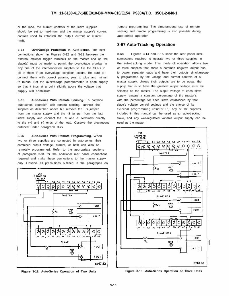
TM 11-6130-417-14/EE010-BK-MMA-010/E154 PS30A/T.O. 35C1-2-848-1
or the load, the current controls of the slave supplies
should be set to maximum and the master supply’s current
controls used to establish the output current or current
limit.
3-64 Overvoltage Protection in Auto-Series. The inter-
connections shown in Figures 3-12 and 3-13 between the
external crowbar trigger terminals on the master and on the
slave(s) must be made to permit the overvoltage crowbar in
any one of the interconnected supplies to fire the SCRs in
all of them if an overvoltage condition occurs. Be sure to
connect them with correct polarity, plus to plus and minus
to minus. Set the overvoltage potentiometer in each supply
so that it trips at a point slightly above the voltage that
supply will contribute.
3-65 Auto-Series With Remote Sensing. To combine
auto-series operation with remote sensing, connect the
supplies as described above but remove the +S jumper
from the master supply and the -S jumper from the last
slave supply and connect the +S and -S terminals directly
to the (+) and (-) ends of the load. Observe the precautions
outlined under paragraph 3-27.
3-66 Auto-Series With Remote Programming. When
two or three supplies are connected in auto-series, their
combined output voltage, current, or both can also be
remotely programmed. Refer to the appropriate sections
of paragraph 3-34 for the additional rear panel connections
required and make these connections to the master supply
only. Observe all precautions outlined in the paragraphs on
remote programming. The simultaneous use of remote
sensing and remote programming is also possible during
auto-series operation.
3-67 Auto-Tracking Operation
3-68 Figures 3-14 and 3-15 show the rear panel inter-
connections required to operate two or three supplies in
the auto-tracking mode. This mode of operation allows two
or three supplies that share a common negative output bus
to power separate loads and have their outputs simultaneous-
ly programmed by the voltage and current controls of a
master supply. Unless their outputs are to be equal, the
supply that is to have the greatest output voltage must be
selected as the master. The output voltage of each slave
supply remains a constant percentage of the master’s
with the percentage for each slave established by that
slave’s voltage control settings and the choice of its
external programming resistor RX. Any of the supplies
included in this manual can be used as an auto-tracking
slave, and any well-regulated variable output supply can be
used as the master.
Figure 3-12. Auto-Series Operation of Two Units
3-10
Figure 3-13. Auto-Series Operation of Three Units
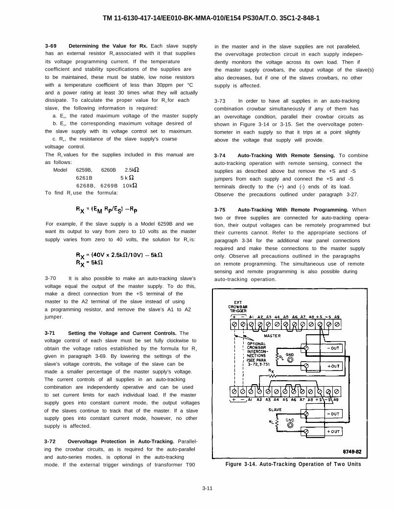
TM 11-6130-417-14/EE010-BK-MMA-010/E154 PS30A/T.O. 35C1-2-848-1
3-69 Determining the Value for Rx. Each slave supplyhas an external resistor RX associated with it that supplies
its voltage programming current. If the temperature
coefficient and stability specifications of the supplies are
to be maintained, these must be stable, low noise resistors
with a temperature coefficient of less than 30ppm per °C
and a power rating at least 30 times what they will actually
dissipate. To calculate the proper value for RX for each
slave, the following information is required:
a. ES, the rated maximum voltage of the master supply
b. ES, the corresponding maximum voltage desired of
the slave supply with its voltage control set to maximum.
c. RP, the resistance of the slave supply’s coarse
voltsage control.
The RP values for the supplies included in this manual are
as follows:
Model 6259B, 6260B 2.5k
6261B 5 k
6268B, 6269B 10kTo find RX use the formula:
For example, if the slave supply is a Model 6259B and we
want its output to vary from zero to 10 volts as the master
supply varies from zero to 40 volts, the solution for RX is:
3-70 It is also possible to make an auto-tracking slave’s
voltage equal the output of the master supply. To do this,
make a direct connection from the +S terminal of the
master to the A2 terminal of the slave instead of using
a programming resistor, and remove the slave’s A1 to A2jumper.
3-71 Setting the Voltage and Current Controls. Thevoltage control of each slave must be set fully clockwise to
obtain the voltage ratios established by the formula for RX
given in paragraph 3-69. By lowering the settings of the
slave’s voltage controls, the voltage of the slave can be
made a smaller percentage of the master supply’s voltage.
The current controls of all supplies in an auto-tracking
combination are independently operative and can be used
to set current limits for each individual load. If the master
supply goes into constant current mode, the output voltages
of the slaves continue to track that of the master. If a slave
supply goes into constant current mode, however, no other
supply is affected.
3-72 Overvoltage Protection in Auto-Tracking. Parallel-
ing the crowbar circuits, as is required for the auto-parallel
and auto-series modes, is optional in the auto-tracking
mode. If the external trigger windings of transformer T90
in the master and in the slave supplies are not paralleled,
the overvoltage protection circuit in each supply indepen-
dently monitors the voltage across its own load. Then if
the master supply crowbars, the output voltage of the slave(s)
also decreases, but if one of the slaves crowbars, no other
supply is affected.
3-73 In order to have all supplies in an auto-tracking
combination crowbar simultaneously if any of them has
an overvoltage condition, parallel their crowbar circuits as
shown in Figure 3-14 or 3-15. Set the overvoltage poten-
tiometer in each supply so that it trips at a point slightly
above the voltage that supply will provide.
3-74 Auto-Tracking With Remote Sensing. To combine
auto-tracking operation with remote sensing, connect the
supplies as described above but remove the +S and -S
jumpers from each supply and connect the +S and -S
terminals directly to the (+) and (-) ends of its load.
Observe the precautions outlined under paragraph 3-27.
3-75 Auto-Tracking With Remote Programming. When
two or three supplies are connected for auto-tracking opera-tion, their output voltages can be remotely programmed but
their currents cannot. Refer to the appropriate sections of
paragraph 3-34 for the additional rear panel connections
required and make these connections to the master supply
only. Observe all precautions outlined in the paragraphs
on remote programming. The simultaneous use of remote
sensing and remote programming is also possible during
auto-tracking operation.
Figure 3-14. Auto-Tracking Operation of Two Units
3-11
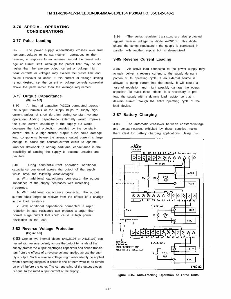
TM 11-6130-417-14/EE010-BK-MMA-010/E154 PS30A/T.O. 35C1-2-848-1
3-76 SPECIAL OPERATINGCONSIDERATIONS
3-77 Pulse Loading
3-78 The power supply automatically crosses over from
constant-voltage to constant-current operation, or the
reverse, in response to an increase beyond the preset volt-
age or current limit. Although the preset limit may be set
higher than the average output current or voltage, high
peak currents or voltages may exceed the preset limit and
cause crossover to occur. If this current or voltage limiting
is not desired, set the current or voltage controls somewhat
above the peak rather than the average requirement.
3-79 Output Capacitance(Figure 6-2)
3-80 An internal capacitor (A3C3) connected across
the output terminals of the supply helps to supply high-
current pulses of short duration during constant voltage
operation. Adding capacitance externally would improve
the pulse current capability of the supply but would
decrease the load protection provided by the constant-
current circuit. A high-current output pulse could damage
load components before the average output current is large
enough to cause the constant-current circuit to operate.
Another drawback to adding additional capacitance is the
possibility of causing the supply to become unstable and
oscillate.
3-81 During constant-current operation, additional
capacitance connected across the output of the supply
would have the following disadvantages:
a. With additional capacitance connected, the output
impedance of the supply decreases with increasing
frequency.
b. With additional capacitance connected, the output
current takes longer to recover from the effects of a change
in the load resistance.
c. With additional capacitance connected, a rapid
reduction in load resistance can produce a larger than
normal surge current that could cause a high power
dissipation in the load.
3-82 Reverse Voltage Protection(Figure 6-5)
3-83 One or two internal diodes (A4CR106 or A4CR107) con-
nected with reverse polarity across the output terminals of the
supply protect the output electrolytic capacitors and series transis-
tors from the effects of a reverse voltage applied across the sup-
ply’s output. Such a reverse voltage might inadvertently be applied
when operating supplies in series if one of them were to be turned
on or off before the other. The current rating of the output diodes
is equal to the rated output current of the supply.
3-84 The series regulator transistors are also protected
against reverse voltage by diode A4CR105. This diode
shunts the series regulators if the supply is connected in
parallel with another supply but is deenergized.
3-85 Reverse Current Loading
3-86 An active load connected to the power supply may
actually deliver a reverse current to the supply during a
portion of its operating cycle. If an external source is
allowed to pump current into the supply, it will cause a
loss of regulation and might possibly damage the outputcapacitor. To avoid these effects, it is necessary to pre-
Ioad the supply with a dummy load resistor so that it
delivers current through the entire operating cycle of the
load device.
3-87 Battery Charging
3-88 The automatic crossover between constant-voltage
and constant-current exhibited by these supplies makes
them ideal for battery charging applications. Using this
Figure 3-15. Auto-Tracking Operation of Three Units
3-12
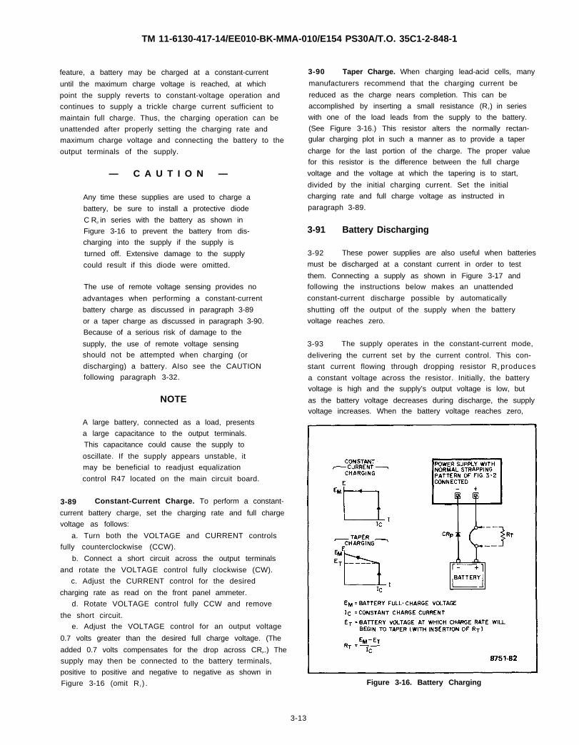
TM 11-6130-417-14/EE010-BK-MMA-010/E154 PS30A/T.O. 35C1-2-848-1
feature, a battery may be charged at a constant-current
until the maximum charge voltage is reached, at which
point the supply reverts to constant-voltage operation and
continues to supply a trickle charge current sufficient to
maintain full charge. Thus, the charging operation can be
unattended after properly setting the charging rate and
maximum charge voltage and connecting the battery to the
output terminals of the supply.
3-89
— C A U T I O N —
Any time these supplies are used to charge a
battery, be sure to install a protective diode
C RP in series with the battery as shown in
Figure 3-16 to prevent the battery from dis-
charging into the supply if the supply is
turned off. Extensive damage to the supply
could result if this diode were omitted.
The use of remote voltage sensing provides no
advantages when performing a constant-current
battery charge as discussed in paragraph 3-89
or a taper charge as discussed in paragraph 3-90.
Because of a serious risk of damage to the
supply, the use of remote voltage sensing
should not be attempted when charging (or
discharging) a battery. AIso see the CAUTION
following paragraph 3-32.
NOTE
A large battery, connected as a load, presents
a large capacitance to the output terminals.
This capacitance could cause the supply to
oscillate. If the supply appears unstable, it
may be beneficial to readjust equalization
control R47 located on the main circuit board.
Constant-Current Charge. To perform a constant-
current battery charge, set the charging rate and full charge
voltage as follows:
a. Turn both the VOLTAGE and CURRENT controls
fully counterclockwise (CCW).
b. Connect a short circuit across the output terminals
and rotate the VOLTAGE control fully clockwise (CW).
c. Adjust the CURRENT control for the desired
charging rate as read on the front panel ammeter.
d. Rotate VOLTAGE control fully CCW and remove
the short circuit.
e. Adjust the VOLTAGE control for an output voltage
0.7 volts greater than the desired full charge voltage. (The
added 0.7 volts compensates for the drop across CRP.) The
supply may then be connected to the battery terminals,
positive to positive and negative to negative as shown in
Figure 3-16 (omit RT) .
3-90 Taper Charge. When charging lead-acid cells, many
manufacturers recommend that the charging current be
reduced as the charge nears completion. This can be
accomplished by inserting a small resistance (RT) in series
with one of the load leads from the supply to the battery.
(See Figure 3-16.) This resistor alters the normally rectan-gular charging plot in such a manner as to provide a taper
charge for the last portion of the charge. The proper value
for this resistor is the difference between the full charge
voltage and the voltage at which the tapering is to start,
divided by the initial charging current. Set the initial
charging rate and full charge voltage as instructed in
paragraph 3-89.
3-91 Battery Discharging
3-92 These power supplies are also useful when batteries
must be discharged at a constant current in order to test
them. Connecting a supply as shown in Figure 3-17 and
following the instructions below makes an unattended
constant-current discharge possible by automatically
shutting off the output of the supply when the battery
voltage reaches zero.
3-93 The supply operates in the constant-current mode,
delivering the current set by the current control. This con-
stant current flowing through dropping resistor RX produces
a constant voltage across the resistor. Initially, the battery
voltage is high and the supply’s output voltage is low, but
as the battery voltage decreases during discharge, the supplyvoltage increases. When the battery voltage reaches zero,
Figure 3-16. Battery Charging
3-13
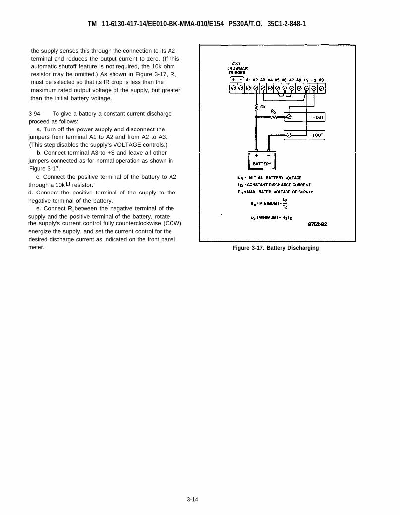
TM 11-6130-417-14/EE010-BK-MMA-010/E154 PS30A/T.O. 35C1-2-848-1
the supply senses this through the connection to its A2terminal and reduces the output current to zero. (If thisautomatic shutoff feature is not required, the 10k ohmresistor may be omitted.) As shown in Figure 3-17, RX
must be selected so that its IR drop is less than themaximum rated output voltage of the supply, but greaterthan the initial battery voltage.
3-94 To give a battery a constant-current discharge,proceed as follows:
a. Turn off the power supply and disconnect thejumpers from terminal A1 to A2 and from A2 to A3.(This step disables the supply’s VOLTAGE controls.)
b. Connect terminal A3 to +S and leave all otherjumpers connected as for normal operation as shown inFigure 3-17.
c. Connect the positive terminal of the battery to A2through a 10k resistor.d. Connect the positive terminal of the supply to thenegative terminal of the battery.
e. Connect RX between the negative terminal of thesupply and the positive terminal of the battery, rotatethe supply’s current control fully counterclockwise (CCW),energize the supply, and set the current control for thedesired discharge current as indicated on the front panelmeter. Figure 3-17. Battery Discharging
3-14
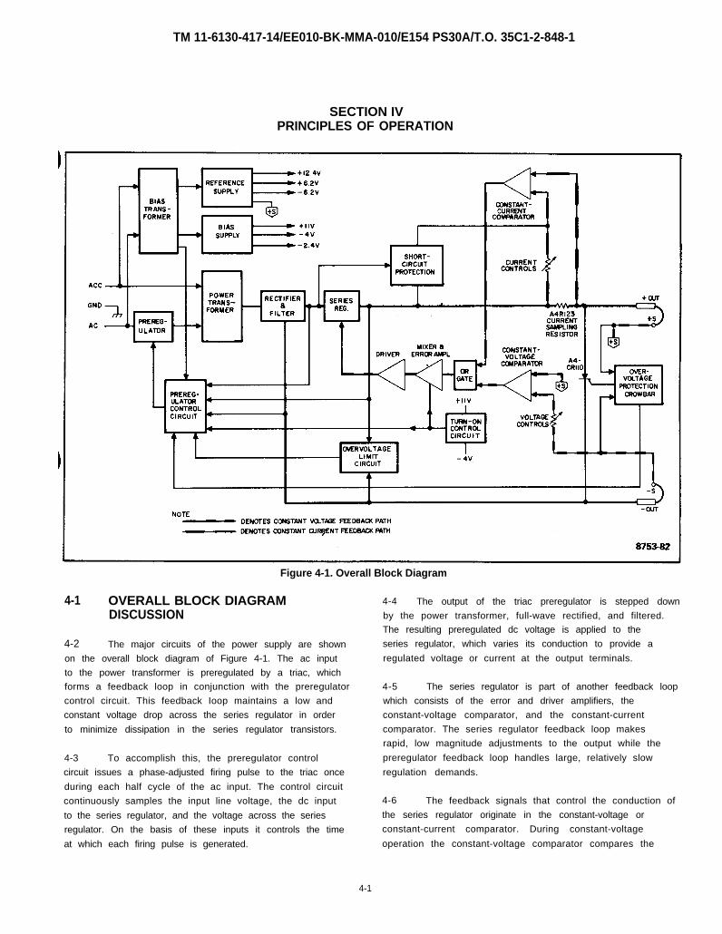
TM 11-6130-417-14/EE010-BK-MMA-010/E154 PS30A/T.O. 35C1-2-848-1
SECTION IVPRINCIPLES OF OPERATION
Figure 4-1. Overall Block Diagram
4-1 OVERALL BLOCK DIAGRAMDISCUSSION
4-2 The major circuits of the power supply are shown
on the overall block diagram of Figure 4-1. The ac input
to the power transformer is preregulated by a triac, which
forms a feedback loop in conjunction with the preregulator
control circuit. This feedback Ioop maintains a low and
constant voltage drop across the series regulator in order
to minimize dissipation in the series regulator transistors.
4-3 To accomplish this, the preregulator control
circuit issues a phase-adjusted firing pulse to the triac once
during each half cycle of the ac input. The control circuit
continuously samples the input line voltage, the dc input
to the series regulator, and the voltage across the series
regulator. On the basis of these inputs it controls the time
at which each firing pulse is generated.
4-4 The output of the triac preregulator is stepped down
by the power transformer, full-wave rectified, and filtered.
The resulting preregulated dc voltage is applied to the
series regulator, which varies its conduction to provide a
regulated voltage or current at the output terminals.
4-5 The series regulator is part of another feedback loop
which consists of the error and driver amplifiers, the
constant-voltage comparator, and the constant-current
comparator. The series regulator feedback loop makes
rapid, low magnitude adjustments to the output while the
preregulator feedback loop handles large, relatively slow
regulation demands.
4-6 The feedback signals that control the conduction of
the series regulator originate in the constant-voltage or
constant-current comparator. During constant-voltage
operation the constant-voltage comparator compares the
4-1
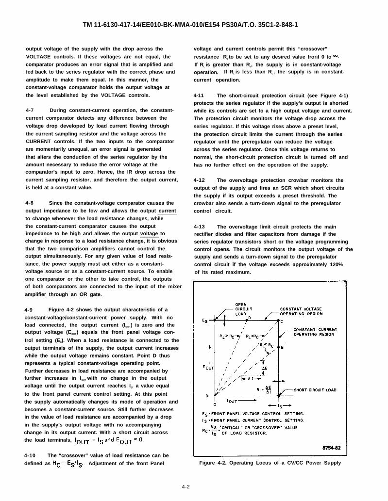
TM 11-6130-417-14/EE010-BK-MMA-010/E154 PS30A/T.O. 35C1-2-848-1
output voltage of the supply with the drop across the
VOLTAGE controls. If these voltages are not equal, the
comparator produces an error signal that is amplified andfed back to the series regulator with the correct phase and
amplitude to make them equal. In this manner, theconstant-voltage comparator holds the output voltage at
the level established by the VOLTAGE controls.
4-7 During constant-current operation, the constant-
current comparator detects any difference between the
voltage drop developed by load current flowing through
the current sampling resistor and the voltage across theCURRENT controls. If the two inputs to the comparator
are momentarily unequal, an error signal is generated
that alters the conduction of the series regulator by theamount necessary to reduce the error voltage at thecomparator’s input to zero. Hence, the IR drop across the
current sampling resistor, and therefore the output current,
is held at a constant value.
4-8 Since the constant-voltage comparator causes the
output impedance to be low and allows the output current
to change whenever the load resistance changes, while
the constant-current comparator causes the outputimpedance to be high and allows the output voltage tochange in response to a load resistance change, it is obvious
that the two comparison amplifiers cannot control theoutput simultaneously. For any given value of load resis-
tance, the power supply must act either as a constant-voltage source or as a constant-current source. To enable
one comparator or the other to take control, the outputsof both comparators are connected to the input of the mixer
amplifier through an OR gate.
4-9 Figure 4-2 shows the output characteristic of a
constant-voltage/constant-current power supply. With noload connected, the output current (lOUT) is zero and theoutput voltage (EOUT) equals the front panel voltage con-
trol setting (ES). When a load resistance is connected to the
output terminals of the supply, the output current increaseswhile the output voltage remains constant. Point D thusrepresents a typical constant-voltage operating point.
Further decreases in load resistance are accompanied byfurther increases in IOUT with no change in the outputvoltage until the output current reaches IS, a value equal
to the front panel current control setting. At this point
the supply automatically changes its mode of operation and
becomes a constant-current source. Still further decreasesin the value of load resistance are accompanied by a drop
in the supply’s output voltage with no accompanyingchange in its output current. With a short circuit acrossthe load terminals,
4-10 The “crossover” value of load resistance can be
defined as Adjustment of the front Panel
voltage and current controls permit this “crossover”
resistance Rc to be set to any desired value froril 0 to
If RL is greater than Rc, the supply is in constant-voltage
operation. If RL is less than RC, the supply is in constant-
current operation.
4-11 The short-circuit protection circuit (see Figure 4-1)protects the series regulator if the supply’s output is shortedwhile its controls are set to a high output voltage and current.
The protection circuit monitors the voltage drop across the
series regulator. If this voltage rises above a preset level,
the protection circuit limits the current through the seriesregulator until the preregulator can reduce the voltage
across the series regulator. Once this voltage returns to
normal, the short-circuit protection circuit is turned off and
has no further effect on the operation of the supply.
4-12 The overvoltage protection crowbar monitors the
output of the supply and fires an SCR which short circuits
the supply if its output exceeds a preset threshold. Thecrowbar also sends a turn-down signal to the preregulator
control circuit.
4-13 The overvoltage limit circuit protects the mainrectifier diodes and filter capacitors from damage if theseries regulator transistors short or the voltage programmingcontrol opens. The circuit monitors the output voltage of thesupply and sends a turn-down signal to the preregulator
control circuit if the voltage exceeds approximately 120%
of its rated maximum.
Figure 4-2. Operating Locus of a CV/CC Power Supply
4-2
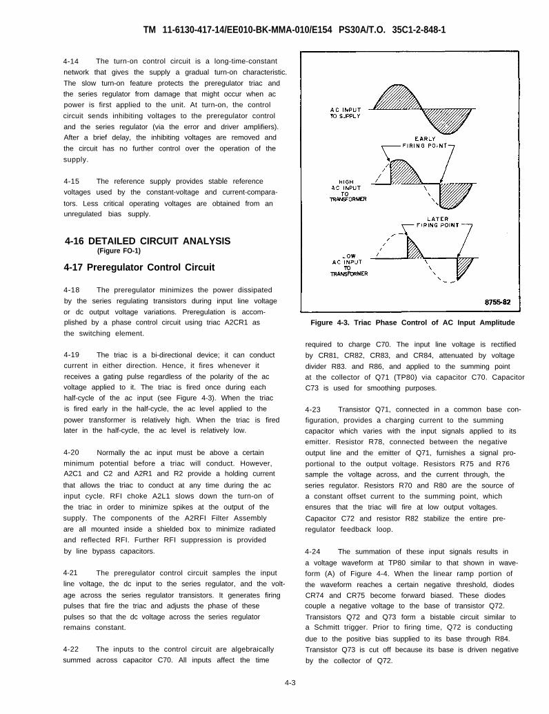
TM 11-6130-417-14/EE010-BK-MMA-010/E154 PS30A/T.O. 35C1-2-848-1
4-14 The turn-on control circuit is a long-time-constant
network that gives the supply a gradual turn-on characteristic.
The slow turn-on feature protects the preregulator triac and
the series regulator from damage that might occur when ac
power is first applied to the unit. At turn-on, the control
circuit sends inhibiting voltages to the preregulator control
and the series regulator (via the error and driver amplifiers).
After a brief delay, the inhibiting voltages are removed and
the circuit has no further control over the operation of the
supply.
4-15 The reference supply provides stable reference
voltages used by the constant-voltage and current-compara-
tors. Less critical operating voltages are obtained from anunregulated bias supply.
4-16 DETAILED CIRCUIT ANALYSIS(Figure FO-1)
4-17 Preregulator Control Circuit
4-18 The preregulator minimizes the power dissipated
by the series regulating transistors during input line voltage
or dc output voltage variations. Preregulation is accom-plished by a phase control circuit using triac A2CR1 as
the switching element.
4-19 The triac is a bi-directional device; it can conduct
current in either direction. Hence, it fires whenever it
receives a gating pulse regardless of the polarity of the ac
voltage applied to it. The triac is fired once during each
half-cycle of the ac input (see Figure 4-3). When the triac
is fired early in the half-cycle, the ac level applied to the
power transformer is relatively high. When the triac is firedlater in the half-cycle, the ac level is relatively low.
4-20 Normally the ac input must be above a certain
minimum potential before a triac will conduct. However,A2C1 and C2 and A2R1 and R2 provide a holding current
that allows the triac to conduct at any time during the ac
input cycle. RFI choke A2L1 slows down the turn-on of
the triac in order to minimize spikes at the output of the
supply. The components of the A2RFI Filter Assembly
are all mounted inside a shielded box to minimize radiated
and reflected RFI. Further RFI suppression is provided
by line bypass capacitors.
4-21 The preregulator control circuit samples the input
line voltage, the dc input to the series regulator, and the volt-
age across the series regulator transistors. It generates firing
pulses that fire the triac and adjusts the phase of these
pulses so that the dc voltage across the series regulator
remains constant.
4-22 The inputs to the control circuit are algebraically
summed across capacitor C70. All inputs affect the time
Figure 4-3. Triac Phase Control of AC Input Amplitude
required to charge C70. The input line voltage is rectified
by CR81, CR82, CR83, and CR84, attenuated by voltage
divider R83. and R86, and applied to the summing point
at the collector of Q71 (TP80) via capacitor C70. Capacitor
C73 is used for smoothing purposes.
4-23 Transistor Q71, connected in a common base con-
figuration, provides a charging current to the summing
capacitor which varies with the input signals applied to its
emitter. Resistor R78, connected between the negative
output line and the emitter of Q71, furnishes a signal pro-
portional to the output voltage. Resistors R75 and R76
sample the voltage across, and the current through, the
series regulator. Resistors R70 and R80 are the source of
a constant offset current to the summing point, which
ensures that the triac will fire at low output voltages.
Capacitor C72 and resistor R82 stabilize the entire pre-
regulator feedback loop.
4-24 The summation of these input signals results in
a voltage waveform at TP80 similar to that shown in wave-
form (A) of Figure 4-4. When the linear ramp portion of
the waveform reaches a certain negative threshold, diodes
CR74 and CR75 become forward biased. These diodescouple a negative voltage to the base of transistor Q72.
Transistors Q72 and Q73 form a bistable circuit similar toa Schmitt trigger. Prior to firing time, Q72 is conducting
due to the positive bias supplied to its base through R84.
Transistor Q73 is cut off because its base is driven negative
by the collector of Q72.
4-3
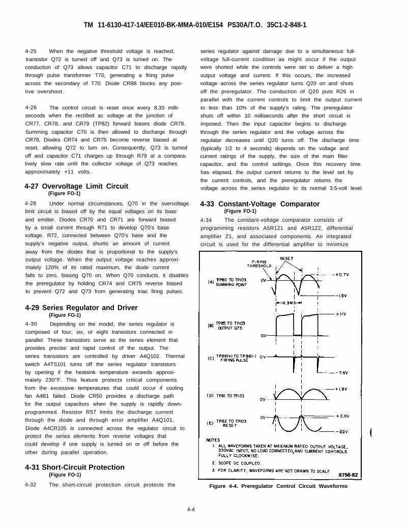
TM 11-6130-417-14/EE010-BK-MMA-010/E154 PS30A/T.O. 35C1-2-848-1
4-25 When the negative threshold voltage is reached,
transistor Q72 is turned off and Q73 is turned on. The
conduction of Q73 allows capacitor C71 to discharge rapidly
through pulse transformer T70, generating a firing pulse
across the secondary of T70. Diode CR88 blocks any posi-
tive overshoot.
4-26 The control circuit is reset once every 8.33 milli-
seconds when the rectified ac voltage at the junction of
CR77, CR78, and CR79 (TP82) forward biases diode CR78.
Summing capacitor C70 is then allowed to discharge through
CR78, Diodes CR74 and CR75 become reverse biased at
reset, allowing Q72 to turn on. Consequently, Q73 is turned
off and capacitor C71 charges up through R79 at a compara-
tively slow rate until the collector voltage of Q73 reaches
approximately +11 volts.
4-27 Overvoltage Limit Circuit(Figure FO-1)
4-28 Under normal circumstances, Q70 in the overvoltage
limit circuit is biased off by the equal voltages on its base
and emitter. Diodes CR70 and CR71 are forward biased
by a small current through R71 to develop Q70’s base
voltage. R72, connected between Q70’s base and the
supply’s negative output, shunts an amount of current
away from the diodes that is proportional to the supply’s
output voltage. When the output voltage reaches approxi-
mately 120% of its rated maximum, the diode current
falls to zero, biasing Q70 on. When Q70 conducts, it disables
the preregulator by holding CR74 and CR75 reverse biased
to prevent Q72 and Q73 from generating triac firing pulses.
4-29 Series Regulator and Driver(Figure FO-1)
4-30 Depending on the model, the series regulator is
composed of four, six, or eight transistors connected in
parallel. These transistors serve as the series element that
provides precise and rapid control of the output. The
series transistors are controlled by driver A4Q102. Thermal
switch A4TS101 turns off the series regulator transistors
by opening if the heatsink temperature exceeds approxi-mately 230°F. This feature protects critical components
from the excessive temperatures that could occur if cooling
fan A4B1 failed. Diode CR50 provides a discharge path
for the output capacitors when the supply is rapidly down-
programmed. Resistor R57 limits the discharge current
through the diode and through error amplifier A4Q101.
Diode A4CR105 is connected across the regulator circuit to
protect the series elements from reverse voltages that
could develop if one supply is turned on or off before the
other during parallel operation.
4-31 Short-Circuit Protection(Figure FO-1)
4-32 The short-circuit protection circuit protects the
series regulator against damage due to a simultaneous full-
voltage full-current condition as might occur if the output
were shorted while the controls were set to deliver a high
output voltage and current. If this occurs, the increased
voltage across the series regulator turns Q20 on and shuts
off the preregulator. The conduction of Q20 puts R26 in
parallel with the current controls to limit the output current
to less than 10% of the supply’s rating. The preregulator
shuts off within 10 milliseconds after the short circuit is
imposed. Then the input capacitor begins to discharge
through the series regulator and the voltage across the
regulator decreases until Q20 turns off. The discharge time
(typically 1/2 to 4 seconds) depends on the voltage and
current ratings of the supply, the size of the main filter
capacitor, and the control settings. Once this recovery time
has elapsed, the output current returns to the level set by
the current controls, and the preregulator returns the
voltage across the series regulator to its normal 3.5-volt level.
4-33 Constant-Voltage Comparator(Figure FO-1)
4-34 The constant-voltage comparator consists of
programming resistors A5R121 and A5R122, differential
amplifier Z1, and associated components. An integrated
circuit is used for the differential amplifier to minimize
Figure 4-4. Preregulator Control Circuit Waveforms
4-4
TM 11-6130-417-14/EE010-BK-MMA-010/E154 PS30A/T.O. 35C1-2-848-1
voltage differentials due to mismatched transistors or
temperature differences.
4-35 The constant-voltage comparator compares the
voltage drop across the VOLTAGE controls with the sup-
ply’s output voltage. If a difference exists, it produces an
error voltage proportional to this difference. This error
signal alters the conduction of the series regulator, which
changes the output voltage until it is equal to the voltage
drop across the VOLTAGE controls. Hence, through feed-
back action, the difference between the two inputs to Z1
is held at zero volts.
4-36 One input of the differential amplifier (pin 10) is
connected to the output voltage sensing terminal of the
supply (+S) through impedance equalizing resistor R23.
Resistors R1 and optional resistor R110 zero bias the input.
If the supply is equipped with Option 020 or 040, resistor
R114 and potentiometer R113 provide a variable input bias
that allows the output voltage to be easily adjusted to
exactly zero volts when the supply is programmed for zero
output. The other input of the differential amplifier (pin 1)
is connected to the summing point (terminal A2) at the
junction of the programming resistors and current pullout
resistors R3, R4, and R5. Instantaneous changes in the output
voltage or changes in the voltage at the summing point due
to changes in the VOLTAGE control setting produce a
difference voltage between the two inputs of the differential
amplifier. This difference voltage is amplified and appears
at the output of the differential amplifier (pin 12) as an
error voltage which ultimately varies the conduction of the
series regulator.
4-37 Resistor R6, in series with the summing point
input to the differential amplifier, limits the current flow-
ing into the differential amplifier during rapid voltage turn-
down. Diode CR7 prevents excessive current drain from
the +6.2 volt reference supply during rapid down-program-
ming. Diodes CR5 and CR6 prevent excessive voltage
excursions from overdriving the differential amplifier.
4-38 During constant-voltage operation, the program-
ming current flowing through the programming resistors
(VOLTAGE controls) is constant because the summing
point is held constant at zero volts by feedback action
and virtually all of the reference supply current flowing
through pull-out resistors R3, R4, and R5 flows through
VOLTAGE controls A5R121 and A5R122. Linear constant-
voltage programming is thus assured. Resistor R3 serves as
a trimming adjustment for the programming current flowing
through A5R121 and A5R122. If the supply is equipped
with Option 020 or 040, resistor R111 and potentiometer
R112 allow the programming current to be adjusted over a
narrow range around its nominal value. In practice, this
adjustment sets the power supply output to exactly the
maximum rated voltage when programmed to that level.
4-39 Main output capacitor A3C3, connected across the
output terminals of the supply, stabilizes the series regulator
feedback loop and helps supply high-current pulses of short
duration during constant-voltage operation. An additional
output capacitor (C19) is connected directly across the
output bus bars to maintain a low ac output impedance by
compensating for the inductive reactance of the main output
capacitor at high frequencies. C19 also helps to minimize
output spikes.
4-40 Constant-Current Comparator(Figure FO-1)
4-41 The constant-current comparator is similar in
appearance and operation to the constant voltage compara-
tor. It consists of programming resistors A5R123 and
A5R124, differential amplifier Z1, and associated components.
4-42 The constant-current comparator circuit compares
the voltage drop across the CURRENT controls with the
voltage drop across current sampling resistor A4R123. If a
difference exists, the differential amplifier produces an
error signal proportional to this difference. The remaining
components in the feedback loop (amplifiers and the
series regulator) maintain the drop across the current
sampling resistor, and hence the output current, at a
constant value.
4-43 One input of the differential amplifier (pin 7) is
connected to the output bus through impedance equalizing
resistor R20 and is zero-biased by R21 and optional resistor
R117. Its other input (pin 4) is connected to the summing
point (terminal A6) at the junction of programming resistors
A5R123 and A5R124 and current pullout resistors R30 and
R31. Instantaneous changes in the output current due to
load changes or changes in the voltage at the summing
point due to changes in the CURRENT control setting
produce a difference voltage between the two inputs of the
differential amplifier. This difference voltage is amplified
and appears at the output of the differential amplifier (pin 6)
as an error voltage which ultimately varies the conduction
of the series regulator.
4-44 Resistor R30 serves as a trimming adjustment for
the programming current flowing through A5R123 and
A5R124. If the supply is equipped with Option 021 or
040, resistor R115 and potentiometer R116 allow the
programming current to be adjusted over a narrow range
around its nominal value, and resistor R118 and potentiometer
R119 provide a variable input bias to allow the output
current to be easily adjusted to exactly zero when the supply
is programmed for zero output. Diode CR21 limits excessive
voltage excursions at the summing-point input to the
differential amplifier.
4-5
TM 11-6130-417-14/EE010-BK-MMA-010/E154 PS30A/T.O. 35C1-2-848-1
4-45 Voltage Clamp Circuit(Figure FO-1)
4-46 The voltage clamp circuit keeps the constant-
voltage programming current relatively constant when the
power supply is operating in the constant-current mode.
This is accomplished by clamping terminal A2, the voltage
summing point, to a fixed bias voltage. During constant-
current operation the constant-voltage programming resis-
tors are a shunt load across the output terminals of the
supply. When the output voltage changes, the current
through these resistors also tends to change. Since this
programming current flows through the current sampling
resistor, it is erroneously interpreted as a load change by
the current comparator circuit. The voltage clamp
eliminates this undesirable effect by maintaining the
programming current at a constant level.
4-47 The voltage divider consisting of Z2A, Z2B, and
VR1 back biases CR2 and Q1 during constant-voltage
operation. When the power supply goes into constant-
current operation, CR2 becomes forward biased by thevoltage at pin 12 of Z1. This results in the conduction of
Q1 and the clamping of the summing point at a potential
only sightly more negative than the normal constant-
voltage potential. Clamping this voltage at approximately
the same potential that exists in constant-voltage operation
results in a constant voltage across, and consequently a
constant current through, current pullout resistors R3, R4,
and R5.
4-48 Mixer and Error Amplifiers(Figure FO-1)
4-49 The mixer and error amplifiers amplify the error
signal received from the constant-voltage or constant-
current input circuit to a level sufficient to drive the series
regulator transistors. Mixer amplifier Q41 receives the error
voltage input from either the constant-voltage or constant-
current comparator via the OR-gate diode (CR1 or CR20)
that is conducting at the time. Diode CR1 is forward biased
and CR20 reverse biased during constant-voltage operation.
The reverse is true during constant-current operation.
4-50 Transistor Q40 provides a constant current to
the collector of Q41 and also generates a negative-going
turn-off signal for the series regulator when the unit is
first turned off. Feedback network C41, R47, and R53
shapes the high frequency rolloff in the loop gain response in
order to stabilize the series regulator feedback loop.
4-51 Error amplifiers Q42 and A4Q101 serve as the pre-
driver elements for the series regulator. A4Q101 also provides
a discharge path for the output capacitors in order to allow
faster down-programming and conducts a bleed current for
the series regulator to keep it in its active region when the
supply is set for zero output current. Diode CR44 prevents
A4Q101’s base from going more negative than –3 volts
in order to limit the bleed current through R57 and protect
A4Q101 from damage if a voltage higher than the program-
med output voltage is applied across the output terminals.
4-52 Overvoltage Protection Crowbar
4-53 The overvoltage protection crowbar circuit protects
sensitive loads against the application of an excessively high
voltage, as might result from a series regulator transistor
failure. It accomplishes this by immediately shorting the
output of the supply as soon as a preset threshold voltage
is exceeded. Until silicon controlled rectifier A4CR110 has
been triggered, it acts as an open circuit and has no effect
on the output voltage. Transistors Q91 and Q92 detect an
overvoltage condition and trigger the SCR to fire. When
the SCR fires, it shorts the supply’s output.
4-54 During normal operation, Q92 is biased on by
current through R99, Q91 is kept turned off by Q92, and
CR91 is reverse biased by the voltage divider formed by
resistors R90, R95, and A5R125. Zener diode VR90
provides a stable reference voltage with which the -S
potential is compared. Potentiometer A5R125 (OVER-
VOLTAGE ADJUST) establishes the output voltage at which
CR91 becomes forward biased and turns Q92 off. When 092
turns off, Q91 begins to conduct, sending a positive-going
trigger pulse to A4CR110 and causing it to create a near
short circuit across the output. When A4CR110 fires,
overvoltage lamp A5DS2 turns on, completing a path fora +11V unregulated holding current through A5DS2. (R92
supplies the holding current if the lamp should open.) This
current holds A4CR110 on even after the output voltage
has fallen. A4CR110 remains in conduction until the
supply is turned off. A4R106 protects A4CR108 and
A4CR110 from the large surge current that occurs when
A4CR110 is first fired. CR93 damps out negative over-
shoot in the trigger pulse.
4-55 The firing of A4CR110 biases Q90 into conduction.
This places approximately +11 volts on the cathode of
CR74 in the preregulator control circuit to reverse bias
CR74 and CR75. By preventing transistor Q72 from
turning off, this prevents the generation of any trigger pulses
and turns off the preregulator.
4-56 The crowbar circuit creates an extra current path
during normal operation of the supply, thus changing the
current that flows through the sampling resistor. Diode
CR92 keeps this extra current at a fixed level for which
compensation can then be made in the constant-current
comparator circuit.
4-57 A slaving arrangement for the crowbar circuits in
more than one supply is made possible by an extra
4-6
TM 11-6130-417-14/EE010-BK-MMA-010/E154 PS30A/T.O. 35C1-2-848-1
secondary winding (terminals 5 and 6) on T90. This wind-
ing is connected to terminals on the rear barrier strip marked± EXT. CROWBAR TRIGGER. When two or three units
have these windings connected in parallel, all of their crow-
bars are activated when any one of the crowbars is tripped.
To reset the crowbars in this arrangement, all of the units
must be turned off and then on. Polarity must be observed
when connecting units in this fashion.
4-58 Turn-On Control Circuit(Figure FO-1)
4-59 The turn-on control circuit is a long-time-constant
network which protects the triac and the series regulator
from possible damage during turn-on. When the supply is
first turned on, C35 applies a positive voltage to the anodes
of CR35 and CR36. Diode CR35 couples this voltage to the
cathode of CR74 in the preregulator control circuit to
ensure that it is initially reverse biased. After C35 becomes
sufficiently charged, CR35 becomes reverse biased and the
preregulator control circuit is permitted to fire the triac.
4-60 Diode CR36 performs a similar function for the
series regulator. This diode initially couples a positivevoltage to Q41, which inverts it and applies it to the series
regulator. This negative voltage keeps the regulator cut off
until C35 charges up. Diode CR37 provides a discharge path
for C35 when the supply is turned off.
4-61 Reference Regulator(Figure FO-1)
4-62 The reference circuit is a feedback power supply
similar to the main supply. It provides stable reference
voltages used throughout the unit. All the regulated
reference voltages are derived from dc obtained from full-
wave rectifier CR61 and CR62 and filter capacitor C61.
Zener diodes VR60 and VR61 establish well regulated poten-
tials of +6.2V and -6.2V with respect to common point+S, while the regulator circuit establishes a well regulated
potential of +12.4 volts. Resistor R63 establishes an
optimum bias current through the zener diodes.
4-63 The regulating circuit consists of series regulating
transistor Q60, driver Q61, and differential amplifier Q62
and Q63. The voltage across zener diodes VR60 and VR61
is compared to the voltage across resistor Z2J, and any
difference is amplified by Q62 and Q63. The error voltage
thus appearing at the collector of Q62 is amplified by driver
stage Q61 and applied to series regulator Q60 in the correct
phase and amplitude to maintain the +12.4 volt output at a
constant level.
4-64 Diode CR60, connected from voltage divider R66
and R67 to the base of Q61, serves as a turn-on circuit for
series regulator transistor Q60. When the supply is first
turned on, CR60 biases driver Q61 on, thus turning on the
series regulator. When the reference supply reaches normal
output, the base voltage of Q61 is sufficient to reverse bias
CR60, thus effectively removing it from the circuit. Capa-
citor C60, connected across the output of the reference sup-
ply, removes spikes and stabilizes the reference regulator loop.
4-65 A separate winding on transformer A3T2, diodes
CR53 and CR54, and filter capacitor C44 provide an un-
regulated +11V output. Additional lightly regulated refer-
ence voltages of -2.4 volts and -4 volts are provided by
diodes CR45 through CR49. Resistor R41 biases the diodes.
Diode CR43 prevents reverse current flow from damaging
the main supply series regulator transistor(s). Diode CR7,
shown on the schematic near current pullout resistors R3,
R4, and R5, protects the zener diodes in the reference cir-
cuit by providing a path for surge currents that occur
during rapid down-programming.
4-66 Meter Circuit(Figure FO-1)
4-67 The front panel voltmeter and ammeter provide
continuous indications of output voltage and current.
Both meter movements can withstand an overload of several
times the maximum rated output without damage.
4-68 The ammeter, together with its series resistors R101
and R105, is connected across current sampling resistor
A4R123, As mentioned previously, the voltage drop across
A4R123 varies in proportion to the output current. Poten-
tiometer R101 permits calibration of the ammeter.
4-69 The voltmeter, in series with R103 and R104 and
shunted by R102 and R106, is connected directly across
the output terminals of the supply. Potentiometer R106
permits calibration of the voltmeter.
4-70 Additional Protection Features(Figure FO-1)
4-71 The supply contains several special purpose com-
ponents that protect it in the event of unusual circumstances.
One of these components is diode A4CR106 (and A4CR107).
Connected across the output terminals of the supply, it
prevents internal damage from reverse voltages that might
be applied across the supply. This could occur, for example,
during Auto-Series operation if one supply were turned on
or off before the other.
4-72 Resistors R108 and R109 limit the output of the
supply if the jumpers between the output buses and the
sensing terminals (+S and -S) are inadvertently removed.
4-73 Diode A4CR105, previously mentioned in the
series regulator description, protects the regulating
transistor from reverse voltages.
4-7/(4-8 blank)

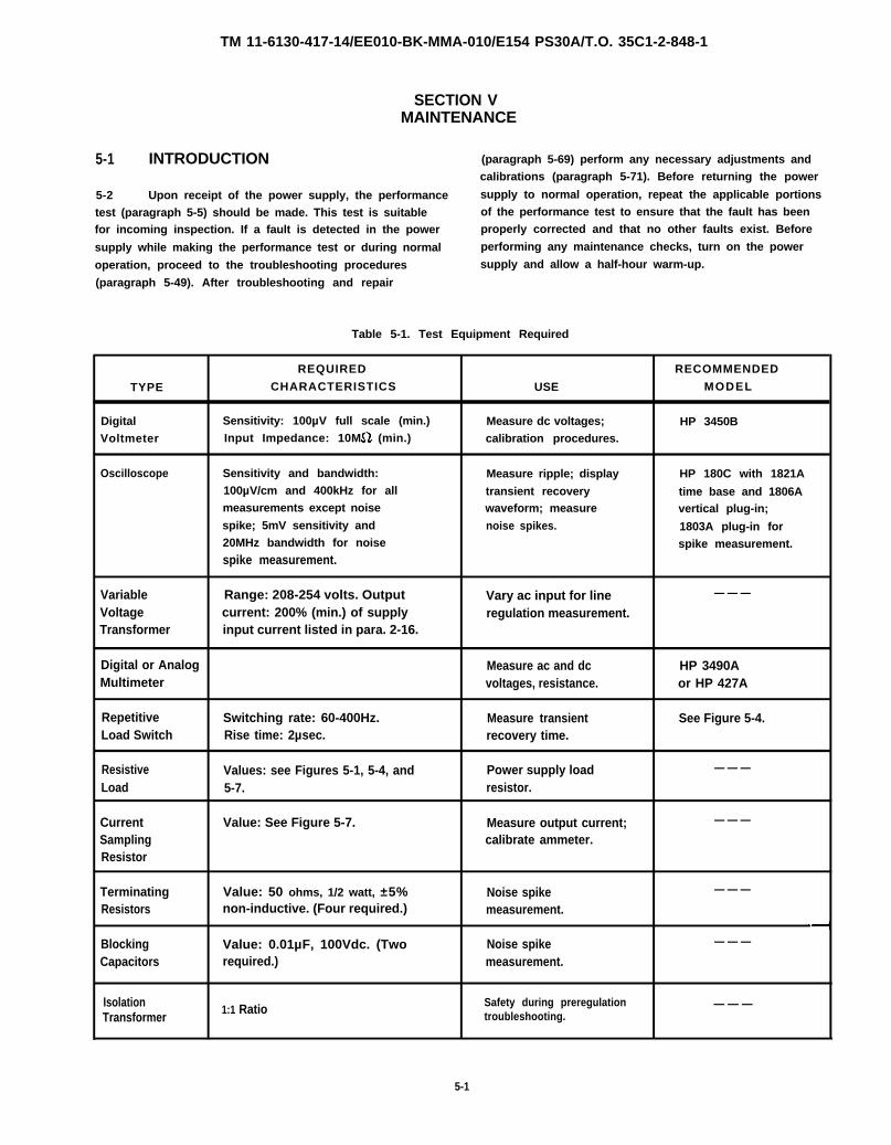
TM 11-6130-417-14/EE010-BK-MMA-010/E154 PS30A/T.O. 35C1-2-848-1
SECTION VMAINTENANCE
5-1 INTRODUCTION (paragraph 5-69) perform any necessary adjustments andcalibrations (paragraph 5-71). Before returning the power
5-2 Upon receipt of the power supply, the performance supply to normal operation, repeat the applicable portions
test (paragraph 5-5) should be made. This test is suitable of the performance test to ensure that the fault has been
for incoming inspection. If a fault is detected in the power properly corrected and that no other faults exist. Before
supply while making the performance test or during normal performing any maintenance checks, turn on the power
operation, proceed to the troubleshooting procedures supply and allow a half-hour warm-up.
(paragraph 5-49). After troubleshooting and repair
Table 5-1. Test Equipment Required
REQUIRED RECOMMENDED
TYPE CHARACTERISTICS USE MODEL
Digital Sensitivity: 100µV full scale (min.) Measure dc voltages; HP 3450BVoltmeter Input Impedance: 10M (min.) calibration procedures.
Oscilloscope Sensitivity and bandwidth: Measure ripple; display HP 180C with 1821A100µV/cm and 400kHz for all transient recovery time base and 1806Ameasurements except noise waveform; measure vertical plug-in;spike; 5mV sensitivity and noise spikes. 1803A plug-in for20MHz bandwidth for noise spike measurement.spike measurement.
Variable Range: 208-254 volts. Output Vary ac input for line — — —
Voltage current: 200% (min.) of supply regulation measurement.Transformer input current listed in para. 2-16.
Digital or Analog Measure ac and dc HP 3490AMultimeter voltages, resistance. or HP 427A
Repetitive Switching rate: 60-400Hz. Measure transient See Figure 5-4.Load Switch Rise time: 2µsec. recovery time.
Resistive Values: see Figures 5-1, 5-4, and Power supply load — — —
Load 5-7. resistor.
Current Value: See Figure 5-7. Measure output current; — — —
Sampling calibrate ammeter.Resistor
Terminating Value: 50 ohms, 1/2 watt, ±5% Noise spike — — —
Resistors non-inductive. (Four required.) measurement.
Blocking Value: 0.01µF, 100Vdc. (Two Noise spike — — —
Capacitors required.) measurement.
Isolation1:1 Ratio Safety during preregulation
Transformer— — —
troubleshooting.
5-1
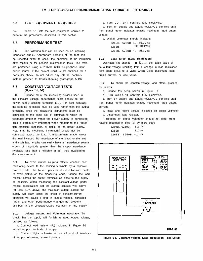
TM 11-6130-417-14/EE010-BK-MMA-010/E154 PS30A/T.O. 35C1-2-848-1
5-3 T E S T E Q U I P M E N T R E Q U I R E D
5-4 Table 5-1 Iists the test equipment required to
perform the procedures described in this section.
5-5 PERFORMANCE TEST
5-6 The following test can be used as an incoming
inspection check. Appropriate portions of the test can
be repeated either to check the operation of the instrument
after repairs or for periodic maintenance tests. The tests
are performed using a 230Vac 60Hz single-phase input
power source. If the correct result is not obtained for a
particular check, do not adjust any internal controls;
instead proceed to troubleshooting (paragraph 5-49).
5-7 CONSTANT-VOLTAGE TESTS(Figure 2-1, 5-1)
5-8 Connect all of the measuring devices used in
the constant voltage performance tests directly to the
power supply sensing terminals (±S). For best accuracy,
the sensing terminals must be used rather than the output
terminals, since the measuring instruments must be
connected to the same pair of terminals to which the
feedback amplifier within the power supply is connected.
This is particularly important when measuring the regula-
tion, transient response, or ripple of the power supply.Note that the measuring instruments should not be
connected across the load. A measurement made across
the load includes the impedance of the leads to the load
and such lead lengths can easily have an impedance several
orders of magnitude greater than the supply impedance
(typically less than 1 milliohm at dc), thus invalidatingthe measurement.
5-9 To avoid mutual coupling effects, connect each
monitoring device to the sensing terminals by a separate
pair of leads. Use twisted pairs or shielded two-wire cables
to avoid pickup on the measuring leads. Connect the load
resistor across the output terminals as close to the supply
as possible. When measuring the constant-voltage perfor-
mance specifications set the current controls well above
(at least 10% above) the maximum output current the
supply will draw, since the onset of constant-current
operation will cause a drop in output voltage, increased
ripple, and other performance changes not properly
ascribed to the constant-voltage operation of the supply.
5-10 Voltage Output and Voltmeter Accuracy. To
check that the supply will furnish its rated output voltage,
proceed as folIows:
a. Connect load resistor (RL) indicated in Figure 5-1
across output terminals of supply.
b. Connect digital voltmeter across +S and -S terminals
of supply, observing correct polarity.
c. Turn CURRENT controls fully clockwise.
d. Turn on supply and adjust VOLTAGE controls until
front panel meter indicates exactly maximum rated output
voltage.
e. Digital voltmeter should indicate:
6259B, 6260B 10 ±0.2Vdc
6261B 20 ±0.4Vdc
6268B, 6269B 40 ±0.8Vdc
5-11 Load Effect (Load Regulation).
Definition: The change E OUTin the static value of
dc output voltage resulting from a change in load resistance
from open circuit to a value which yields maximum rated
output current, or vice versa.
5-12 To check the constant-voltage load effect, proceed
as follows:
a. Connect test setup shown in Figure 5-1.
b. Turn CURRENT controls fully clockwise.
c. Turn on supply and adjust VOLTAGE controls until
front panel meter indicates exactly maximum rated output
current.
d. Read and record voltage indicated on digital voltmeter.
e. Disconnect load resistor.
f. Reading on digital voltmeter should not differ from
reading recorded in step (d) by more than:
6259B, 6260B 1.2mV
6261B 2.2mV
6268B, 6269B 4.2mV
Figure 5-1. Constant-Voltage Load Regulation Test Setup
5-2
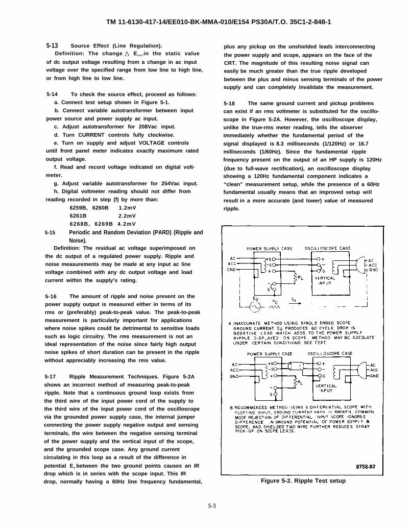
TM 11-6130-417-14/EE010-BK-MMA-010/E154 PS30A/T.O. 35C1-2-848-1
5-13 Source Effect (Line Regulation).Definition: The change EO U T in the static value
of dc output voltage resulting from a change in ac inputvoltage over the specified range from low line to high line,
or from high line to low line.
5-14 To check the source effect, proceed as follows:a. Connect test setup shown in Figure 5-1.
b. Connect variable autotransformer between input
power source and power supply ac input.c. Adjust autotransformer for 208Vac input.
d. Turn CURRENT controls fully clockwise.e. Turn on supply and adjust VOLTAGE controls
until front panel meter indicates exactly maximum rated
output voltage.f. Read and record voltage indicated on digital volt-
meter.
g. Adjust variable autotransformer for 254Vac input.h. Digital voltmeter reading should not differ from
reading recorded in step (f) by more than:
6259B, 6260B 1.2mV6261B 2.2mV6268B, 6269B 4.2mV
5-15 Periodic and Random Deviation (PARD) (Ripple andNoise).
Definition: The residual ac voltage superimposed on
the dc output of a regulated power supply. Ripple andnoise measurements may be made at any input ac linevoltage combined with any dc output voltage and load
current within the supply’s rating.
5-16 The amount of ripple and noise present on thepower supply output is measured either in terms of itsrms or (preferably) peak-to-peak value. The peak-to-peakmeasurement is particularly important for applicationswhere noise spikes could be detrimental to sensitive loads
such as logic circuitry. The rms measurement is not anideal representation of the noise since fairly high outputnoise spikes of short duration can be present in the ripple
without appreciably increasing the rms value.
5-17 Ripple Measurement Techniques. Figure 5-2A
shows an incorrect method of measuring peak-to-peakripple. Note that a continuous ground loop exists from
the third wire of the input power cord of the supply tothe third wire of the input power cord of the oscilloscopevia the grounded power supply case, the internal jumperconnecting the power supply negative output and sensing
terminals, the wire between the negative sensing terminal
of the power supply and the vertical input of the scope,and the grounded scope case. Any ground currentcirculating in this loop as a result of the difference in
potential EG between the two ground points causes an IRdrop which is in series with the scope input. This IRdrop, normally having a 60Hz line frequency fundamental,
plus any pickup on the unshielded leads interconnecting
the power supply and scope, appears on the face of theCRT. The magnitude of this resulting noise signal caneasily be much greater than the true ripple developed
between the plus and minus sensing terminals of the powersupply and can completely invalidate the measurement.
5-18 The same ground current and pickup problemscan exist if an rms voltmeter is substituted for the oscillo-
scope in Figure 5-2A. However, the oscilloscope display,unlike the true-rms meter reading, tells the observerimmediately whether the fundamental period of the
signal displayed is 8.3 milliseconds (1/120Hz) or 16.7milliseconds (1/60Hz). Since the fundamental ripplefrequency present on the output of an HP supply is 120Hz
(due to full-wave rectification), an oscilloscope displayshowing a 120Hz fundamental component indicates a
“clean” measurement setup, while the presence of a 60Hzfundamental usually means that an improved setup will
result in a more accurate (and lower) value of measuredripple.
Figure 5-2. Ripple Test setup
5-3
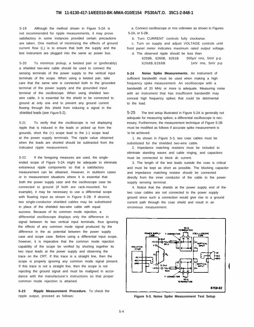
TM 11-6130-417-14/EE010-BK-MMA-010/E154 PS30A/T.O. 35C1-2-848-1
5-19 Although the method shown in Figure 5-2A is
not recommended for ripple measurements, it may prove
satisfactory in some instances provided certain precautions
are taken. One method of minimizing the effects of ground
current flow (lG) is to ensure that both the supply and the
test instrument are plugged into the same ac power bus.
5-20 To minimize pickup, a twisted pair or (preferably)
a shielded two-wire cable should be used to connect the
sensing terminals of the power supply to the vertical input
terminals of the scope. When using a twisted pair, take
care that the same wire is connected both to the grounded
terminal of the power supply and the grounded input
terminal of the oscilloscope. When using shielded two-
wire cable, it is essential for the shield to be connected to
ground at only one end to prevent any ground current
flowing through this shield from inducing a signal in the
shielded leads (see Figure 5-2).
5-21 To verify that the oscilloscope is not displaying
ripple that is induced in the leads or picked up from the
grounds, short the (+) scope lead to the (–) scope lead
at the power supply terminals. The ripple value obtained
when the leads are shorted should be subtracted from the
indicated ripple measurement.
5-22 If the foregoing measures are used, the single-
ended scope of Figure 5-2A might be adequate to eliminate
extraneous ripple components so that a satisfactory
measurement can be obtained, However, in stubborn cases
or in measurement situations where it is essential that
both the power supply case and the oscilIoscope case be
connected to ground (if both are rack-mounted, for
example), it may be necessary to use a differential scope
with floating input as shown in Figure 5-2B. If desired,
two single-conductor shielded cables may be substituted
in place of the shielded two-wire cable with equal
success. Because of its common mode rejection, a
differential oscilloscope displays only the difference in
signal between its two vertical input terminals, thus ignoring
the effects of any common mode signal produced by the
difference in the ac potential between the power supply
case and scope case. Before using a differential input scope,
however, it is imperative that the common mode rejection
capability of the scope be verified by shorting together its
two input leads at the power supply and observing the
trace on the CRT. If this trace is a straight line, then the
scope is properly ignoring any common mode signal present.
If this trace is not a straight line, then the scope is not
rejecting the ground signal and must be realigned in accor-
dance with the manufacturer’s instructions so that proper
common mode rejection is attained.
5-23 Ripple Measurement Procedure. To check the
ripple output, proceed as follows:
a. Connect oscilloscope or rms voltmeter as shown in Figures
5-2A, or 5-2B.
b. Turn CURRENT controls fully clockwise.
c. Turn on supply and adjust VOLTAGE controls until
front panel meter indicates maximum rated output voltage.
d. The observed ripple should be less than:
6259B, 6260B, 6261B 500µV rms, 5mV p-p
6268B,6269B 1mV rms, 5mV p-p
5-24 Noise Spike Measurements. An instrument of
sufficient bandwidth must be used when making a high
frequency spike measurement. An oscilloscope with a
bandwidth of 20 MHz or more is adequate. Measuring noise
with an instrument that has insufficient bandwidth may
conceal high frequency spikes that could be detrimental
to the load.
5-25 The test setup illustrated in Figure 5-2A is generally not
adequate for measuring spikes; a differential oscilloscope is nec-
essary, Furthermore, the measurement technique of Figure 5-2B
must be modified as follows if accurate spike measurement is
to be achieved:
1. As shown in Figure 5-3, two coax cables must be
substituted for the shielded two-wire cable.2. Impedance matching resistors must be included to
eliminate standing waves and cable ringing, and capacitors
must be connected to block dc current.
3. The length of the test leads outside the coax is critical
and must be kept as short as possible. The blocking capacitor
and impedance matching resistor should be connected
directly from the inner conductor of the cable to the power
supply sensing terminal.
4. Notice that the shields at the power supply end of the
two coax cables are not connected to the power supply
ground since such a connection would give rise to a ground
current path through the coax shield and result in an
erroneous measurement.
Figure 5-3. Noise Spike Measurement Test Setup
5-4
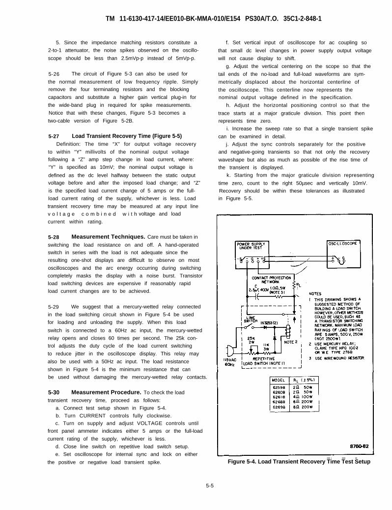
TM 11-6130-417-14/EE010-BK-MMA-010/E154 PS30A/T.O. 35C1-2-848-1
5. Since the impedance matching resistors constitute a
2-to-1 attenuator, the noise spikes observed on the oscillo-
scope should be less than 2.5mVp-p instead of 5mVp-p.
5-26 The circuit of Figure 5-3 can also be used for
the normal measurement of low frequency ripple. Simply
remove the four terminating resistors and the blocking
capacitors and substitute a higher gain vertical plug-in for
the wide-band plug in required for spike measurements.
Notice that with these changes, Figure 5-3 becomes a
two-cable version of Figure 5-2B.
5-27 Load Transient Recovery Time (Figure 5-5)Definition: The time “X” for output voltage recovery
to within “Y” millivolts of the nominal output voltage
following a “Z” amp step change in load current, where:
“Y” is specified as 10mV; the nominal output voltage is
defined as the dc level halfway between the static output
voltage before and after the imposed load change; and “Z”
is the specified load current change of 5 amps or the full-
Ioad current rating of the supply, whichever is less. Load
transient recovery time may be measured at any input line
v o l t a g e c o m b i n e d w i t h voltage and load
current within rating.
5-28 Measurement Techniques. Care must be taken in
switching the load resistance on and off. A hand-operated
switch in series with the load is not adequate since the
resulting one-shot displays are difficult to observe on most
oscilloscopes and the arc energy occurring during switching
completely masks the display with a noise burst. Transistor
load switching devices are expensive if reasonably rapid
load current changes are to be achieved.
5-29 We suggest that a mercury-wetted relay connected
in the load switching circuit shown in Figure 5-4 be used
for loading and unloading the supply. When this load
switch is connected to a 60Hz ac input, the mercury-wetted
relay opens and closes 60 times per second. The 25k con-
trol adjusts the duty cycle of the load current switching
to reduce jitter in the oscilloscope display. This relay may
also be used with a 50Hz ac input. The load resistance
shown in Figure 5-4 is the minimum resistance that can
be used without damaging the mercury-wetted relay contacts.
5-30 Measurement Procedure. To check the load
transient recovery time, proceed as follows:
a. Connect test setup shown in Figure 5-4.
b. Turn CURRENT controls fully clockwise.
c. Turn on supply and adjust VOLTAGE controls until
front panel ammeter indicates either 5 amps or the full-load
current rating of the supply, whichever is less.
d. Close line switch on repetitive load switch setup.
e. Set oscilloscope for internal sync and lock on either
the positive or negative load transient spike.
f. Set vertical input of oscilloscope for ac coupling so
that small dc level changes in power supply output voltage
will not cause display to shift.
g. Adjust the vertical centering on the scope so that the
tail ends of the no-load and full-load waveforms are sym-
metrically displaced about the horizontal centerline of
the oscilloscope. This centerline now represents the
nominal output voltage defined in the specification.
h. Adjust the horizontal positioning control so that the
trace starts at a major graticule division. This point then
represents time zero.
i. Increase the sweep rate so that a single transient spike
can be examined in detail.
j. Adjust the sync controls separately for the positive
and negative-going transients so that not only the recovery
waveshape but also as much as possible of the rise time of
the transient is displayed.
k. Starting from the major graticule division representing
time zero, count to the right 50µsec and vertically 10mV.
Recovery should be within these tolerances as illustrated
in Figure 5-5.
Figure 5-4. Load Transient Recovery Time Test Setup
5-5
TM 11-6130-417-14/EE010-BK-MMA-010/E154 PS30A/T.O. 35C1-2-848-1
Figure 5-5. Load Transient Recovery Time Waveforms
5-31 Temperature Coefficient.Definition: The change in output voltage per degree
Celsius change in the ambient temperature measured
while ac line voltage, output voltage setting, and load
resistance are all held constant.
5-32 The temperature coefficient of a power supply is
measured by placing the power supply in an oven and
varying it over any temperature span within its rating.
(Most HP power supplies are rated for operation from 0°Cto 55°C.) The power supply temperature must be allowed
to stabilize for a sufficient time at each measurement
temperature.
5-33 The temperature coefficient given in the specifi-
cations is the maximum temperature-dependent output
voltage change which will result over any one-degree
interval. The digital voltmeter used to measure the supply’s
output voltage change should be placed outside the oven
and should have a long-term stability adequate to insure
that its drift will not affect the overall measurement
accuracy.
5-34 To check the temperature coefficient, proceed
as follows:
a. Connect load resistance and digital voltmeter as
illustrated in Figure 5-1.
b. Turn CURRENT controls fully clockwise.
c. Turn on supply and adjust front panel VOLTAGE
controls until front panel voltmeter indicates maximum
ratad output voltage (Figure 3-1).
d. Place power supply in temperature-controlled oven
(digitgl voltmeter remains outside oven).
to 30°C and allow 30-minute warm-up.e. Record digital voltmeter reading.
Set temperature
f. Raise temperature to 40°C and allow 30-minute
warm-up.
g. Observe digital voltmeter reading. Difference in
voltage reading between steps (e) and (g) should be less
than:
6259B, 6260B 12mV
6261B 22mV
6268B, 6269B 42mV
5-35 Drift (Stability):Definition: The change in output voltage for the first
eight hours following a 30-minute warm-up period. During
the interval of measurement, input Iine voltage, load resis-
tance, and ambient temperature, are all held constant.
5-36 This measurement is made by monitoring the output
of the power supply on a digital voltmeter over the stated
measurement interval. A strip chart recorder can be used
to provide a permanent record. Place a thermometer near
the supply to verify that the ambient temperature remains
constant during the period of measurement. The supply
should be located away from any source of stray air currents.
If possible, place the supply in an oven and hold it at a
constant temperature. Take care that the measuring
instrument has an eight-hour stability at least an order of
magnitude better than the stability specification of the
power supply being tested. Typically, a supply will drift
less over the eight-hour measurement interval than during
the half-hour warm-up.
5-37 To check the output stability, proceed as follows:
a. Connect load resistance and digital voltmeter as
illustrated in Figure 5-1.
b. Turn CURRENT controls fully clockwise.
c. Turn on supply and adjust front panel VOLTAGE
controls until digital voltmeter indicates maximum rated
output voltage (Figure 3-1).
d. Allow 30-minute warm-up, then record digital
voltmeter reading.
e. After 8 hours, digital voltmeter reading should not
differ from the step (d) reading by more than:
6259B, 6260B 5mV
6261B, 6268B 8mV
6269B 14mV
5-38 CONSTANT-CURRENT TESTS
5-39 The instruments, methods, and precautions for
the proper measurement of constant-current power supply
characteristics are for the most part identical to those
already described for the measurement of constant-voltage
characteristics. There are, however, two main differences:
5-6
TM 11-6130-417-14/EE010-BK-MMA-010/E154 PS30A/T.O. 35C1-2-848-1
First, the power supply performance will be checked
between short circuit and full load rather than open circuit
and full load. Second, a current monitoring resistor is
inserted between the output of the power supply and the
load.
5 - 4 0 For all output current measurements, the current
sampling resistor must be connected as a four-terminal
device in the same manner as a meter shunt would be. The
load current is fed to the extremes of the wire leading to
the resistor while the sampling terminals are located as
close as possible to the resistance element itself (see Figure
5-6). A current sampling resistor should have low noise,
low temperature coefficient (less than 30ppm/°C) and
should be used at no more than 5% of its rated power so
that its temperature rise will be minimized.
NOTE
In case of diffrculty obtaining a low resistance, highcurrent resistor suitable for current sampling, a dupli-cate of the sampling resistor used in this unit(A4R123, or A4R123A and A4R123B) should be or-dered through regular supply channels.
5-41 Current Output and Ammeter Accuracy. To check
that the supply will furnish its rated output current, pro-
ceed as follows:
a. Connect test setup shown in Figure 5-7.b. Turn VOLTAGE controls fu l ly clockwise.
c. Turn on supply and adjust CURRENT controls
until front panel ammeter indicates maximum rated
output current (Figure 3-1).
d. Digital voltmeter should read 0.5 ±0.01 Vdc.
5-42 Load Effect (Load Regulation).Definition: The change lOUT in the static value of
the dc output current resulting from a change in load
resistance from short circuit to a value which yields
maximum rated output voltage, or vice versa.
5-43 To check the constant-current load effect proceed
as follows:
a. Connect test setup shown in Figure 5-7.b. Turn VOLTAGE controls fully clockwise.c. Turn on supply and adjust CURRENT controls until
front panel ammeter indicates exactly maximum ratedoutput current (Figure 3-1).
d. Read and record voltage indicated on digital voltmeter.
e. Short circuit load resistor (RL).f. Digital voltmeter reading should not differ from
reading recorded in step(d) by more than:6259B 110µv6260B 110µv6261B 110µv6268B 134µv6269B 120µv
5-44 Source Effect (Line Regulation).Definition: The change lOUT in the static value of dc
output current resulting from a change in ac input voltageover the specified range from low line to high line or from
high line to Iowline.
5-45 To check source effect, proceed as follows:
a. Connect test setup shown in Figure 5-7.
b. Connect variable autotransformer between input
power source and power supply ac input.
c. Adjust autotransformer for 208Vac input.d. Turn VOLTAGE controls fully clockwise.e. Turn on supply and adjust CURRENT controls until
front panel ammeter reads exactly maximum rated outputcurrent (Figure 3-1).
f. Read and record voltage indicated on digital voltmeter.g. Adjust autotransformer for 254Vac input.h. Digital voltmeter reading should not differ from
reading recorded in step (f) by more than:
6259B 110µV6260B 110µV 6261B 110µv6268B 134µV6269B 120µV
5-46 PARD (Ripple and Noise).Definition: The residual ac current superimposed on
the dc output of a regulated power supply. Ripple andnoise measurements may be made at any input ac line.voltage combined with any dc output voltage and loadcurrent within the supply’s rating.
5-47 Most of the instructions pertaining to the groundloop and pickup problems associated with constant-voltageripple and noise measurement also apply to the measure-ment of constant-current ripple and noise. Figure 5-8ilIustrates the most important precautions to be observedwhen measuring the ripple and noise of a constant-currentFigure 5-6 Current Resistor Connections
5-7
TM 11-6130-417-14/EE010-BK-MMA-010/E154 PS30A/T.O. 35C1-2-848-1
Figure 5-7 Constant-Current Load Regulation test Setup
Figure 5-8. Constant-Current Ripple and Noise Test Setup
supply. The presence of a 120Hz waveform on the oscillo-
scope normally indicates a correct measurement method.
A waveshape having 60Hz as its fundamental component
usually indicates an incorrect measurement setup.
5-48 To check the ripple and noise, proceed as follows:
a. Connect oscilloscope or rms voltmeter as shown inFigures 5-8A, 5-8B or 5-8C.
b. Rotate VOLTAGE controls fully clockwise.
c. Turn on supply and adjust CURRENT controls until
front panel ammeter reads exactly maximum rated output
current (Figure 3-1).
d. The observed ripple and noise should be less than:
6259B 250µV rms
6260B 250µV rms
6261B 250µV rms
6268B 334µV rms
6269B 250µV rms
5-49 TROUBLESHOOTING
5-50 Before attempting to troubleshoot this instrument,
ensure that the fault is with the instrument and not with
an associated circuit. The performance test (paragraphs
5-5 through 5-48) enables this to be determined without
removing the instrument from the cabinet.
5-51 A good understanding of the principles of opera-
tion is a helpful aid in troubleshooting, and it is recom-
mended that the reader review Section IV of the manual
before attempting to troubleshoot the unit in detail. Once
the principles of operation are understood, refer to the
overall troubleshooting procedures in paragraph 5-54 to
locate the symptom and probable cause.
5-52 The schematic diagram contains normal voltage read-
ings adjacent to some test points. (Test points are identified by cir-
cled numbers.) The measurement conditions are Iisted in the
Schematic Notes. Consult the component location diagrams in
Section VI to determine the locations of components and test
points (Figures 6-1 through 6-7, FO-1, FO-3).
5-53 If a component is found to be defective, replace
it and re-conduct the performance test. When a component
is replaced, refer to the repair and replacement (paragraph
5-69) and adjustment and calibration (paragraph 5-71)
sections of this manual.
5-54 OVERALL TROUBLESHOOTINGPROCEDURES
5-55 To locate the cause of trouble, follow steps 1, 2,
and 3 in sequence:
(1) Check for obvious troubles such as a defective
power cord, an input power failure, or a defective meter.
5-8
Table 5-4
Table 5-4
Table 5-4
Table 5-4
TM 11-6130-417-14/EE010-BK-MMA-010/E154 PS30A/T.O. 35C1-2-848-1
Next, remove the top and bottom covers and inspect for open
connections, charred components, or any other visible defects. If
the trouble source cannot be detected by visual inspection,
proceed to step (2) (Figs. 6-3, 6-4).
(2) In almost all cases, the trouble can be caused byincorrect dc bias or reference voltages ; thus, it is a good
practice to check the voltages in Table 5-2 before proceed-
ing with step (3).
(3) Disconnect the load and examine Table 5-3 for
your symptom and its probable cause.
5-56 Table 5-3 contains symptoms and probable causes
of many possible troubles. If either high or low output
voltage is a symptom, Table 5-4 contains the steps necessary
to isolate the trouble to one of the feedback loops and
instructions directing the tester to the proper table for
further isolation. Because of the interactions between loops,
it is necessary to refer to Table 5-4 before proceeding to
Tables 5-5, 5-6, or 5-7.
5-57 Tables 5-5, 5-6, and 5-7 contain troubleshooting
procedures for the series regulator and preregulator feed-
back loops once the fault has been isolated to one of them.
Tables 5-5 and 5-6 contain instructions for driving each
stage into conduction or cut-off. By following the steps in
these tables, the fault can be isolated to a circuit or a
component.
5-58 Table 5-7 contains troubleshooting procedures
for the preregulator feedback loop. Troubleshooting is
accomplished by comparing waveform illustrations with
the waveforms found at various test points and then
checking the components most likely to be at fault.
5-59 After troubleshooting the unit, it may be necessary
to perform one or more of the calibration procedures
given in this section.
WARNING
Some circuits in this power supply are connected
directly to the input ac power line. The red-
painted case and heatsink of the A2 RFI Assembly
are also at ac line potential. Exercise extreme
caution when working on energized circuits.
Table 5-2 Reference and Bias Voltages
(Refer to schematic and component location diagrams In Section VI for test point locations)
Table 5-3 Overall Troubleshooting
5-9
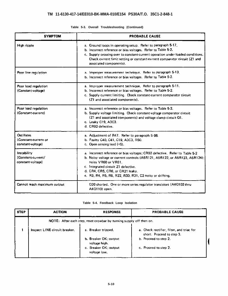
paragraph 5-17
Table 5-2
paragraph 5-13
Table 5-2
paragraph 5-11
Table 5-2
Table 5-2
paragraph 5-98
Table 5-2
TM 11-6130-417-14/EE010-BK-MMA-010/E154 PS30A/T.O. 35C1-2-848-1
Table 5-3. Overall Troubleshooting (Continued)
Table 5-4. Feedback Loop Isolation
5-10
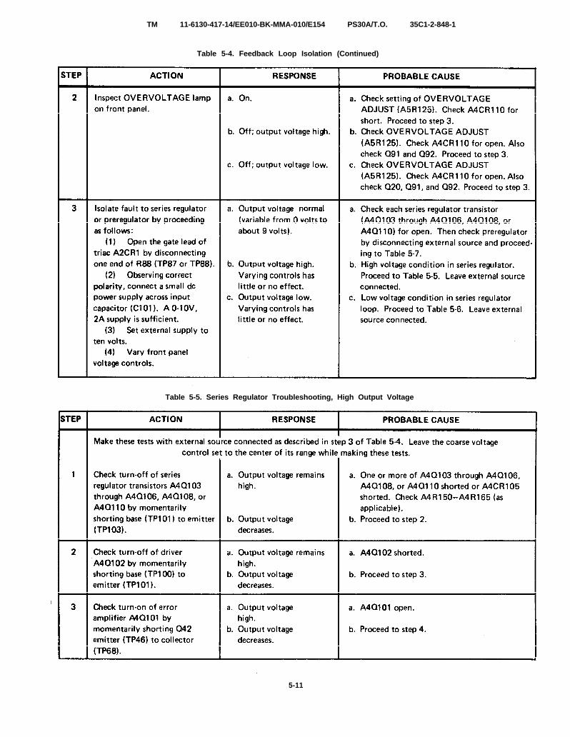
Table 5-7
Table 5-5
Table 5-6
Table 5-4
TM 11-6130-417-14/EE010-BK-MMA-010/E154 PS30A/T.O. 35C1-2-848-1
Table 5-4. Feedback Loop Isolation (Continued)
Table 5-5. Series Regulator Troubleshooting, High Output Voltage
5-11
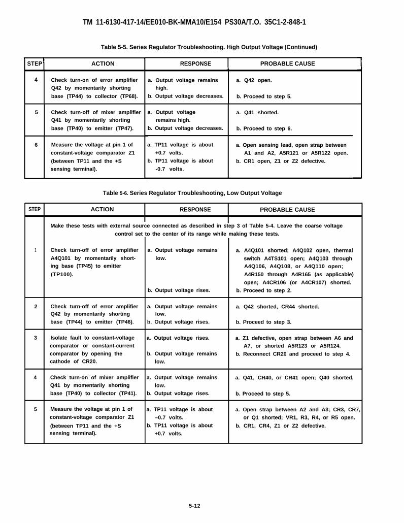
TM 11-6130-417-14/EE010-BK-MMA10/E154 PS30A/T.O. 35C1-2-848-1
Table 5-5. Series Regulator Troubleshooting. High Output Voltage (Continued)
STEP ACTION
4 Check turn-on of error amplifierQ42 by momentarily shorting
base (TP44) to collector (TP68).
5 Check turn-off of mixer amplifierQ41 by momentarily shorting
base (TP40) to emitter (TP47).
6 Measure the voltage at pin 1 of
constant-voltage comparator Z1
(between TP11 and the +Ssensing terminal).
RESPONSE PROBABLE CAUSE
a. Output voltage remains a. Q42 open.high.
b. Output voltage decreases. b. Proceed to step 5.
a. Output voltage a. Q41 shorted.remains high.
b. Output voltage decreases. b. Proceed to step 6.
a. TP11 voltage is about a. Open sensing lead, open strap between+0.7 volts. A1 and A2, A5R121 or A5R122 open.
b. TP11 voltage is about b. CR1 open, Z1 or Z2 defective.-0.7 volts.
Table 5-6. Series Regulator Troubleshooting, Low Output Voltage
STEP ACTION RESPONSE PROBABLE CAUSE
Make these tests with external source connected as described in step 3 of Table 5-4. Leave the coarse voltage
control set to the center of its range while making these tests.
1 Check turn-off of error amplifier a. Output voltage remains a. A4Q101 shorted; A4Q102 open, thermalA4Q101 by momentarily short- low. switch A4TS101 open; A4Q103 throughing base (TP45) to emitter A4Q106, A4Q108, or A4Q110 open;
(TP100). A4R150 through A4R165 (as applicable)
open; A4CR106 (or A4CR107) shorted.b. Output voltage rises. b. Proceed to step 2.
2 Check turn-off of error amplifier a. Output voltage remains a. Q42 shorted, CR44 shorted.Q42 by momentarily shorting low.base (TP44) to emitter (TP46). b. Output voltage rises. b. Proceed to step 3.
3 Isolate fault to constant-voltage a. Output voltage rises. a. Z1 defective, open strap between A6 andcomparator or constant-current A7, or shorted A5R123 or A5R124.comparator by opening the b. Output voltage remains b. Reconnect CR20 and proceed to step 4.cathode of CR20. low.
4 Check turn-on of mixer amplifier a. Output voltage remains a. Q41, CR40, or CR41 open; Q40 shorted.Q41 by momentarily shorting low.base (TP40) to collector (TP41). b. Output voltage rises. b. Proceed to step 5.
5 Measure the voltage at pin 1 of a. TP11 voltage is about a. Open strap between A2 and A3; CR3, CR7,constant-voltage comparator Z1 –0.7 volts. or Q1 shorted; VR1, R3, R4, or R5 open.
(between TP11 and the +S b. TP11 voltage is about b. CR1, CR4, Z1 or Z2 defective.sensing terminal). +0.7 volts.
5-12
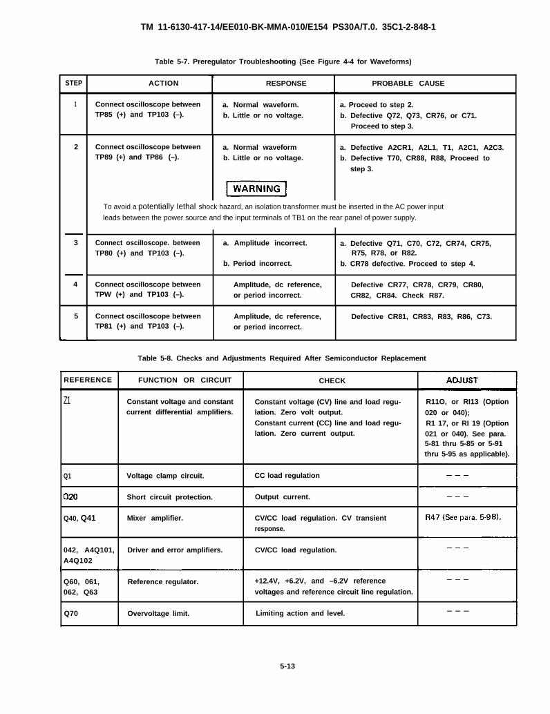
TM 11-6130-417-14/EE010-BK-MMA-010/E154 PS30A/T.0. 35C1-2-848-1
Table 5-7. Preregulator Troubleshooting (See Figure 4-4 for Waveforms)
STEP ACTION RESPONSE PROBABLE CAUSE
1 Connect oscilIoscope between a. Normal waveform. a. Proceed to step 2.TP85 (+) and TP103 (–). b. Little or no voltage. b. Defective Q72, Q73, CR76, or C71.
Proceed to step 3.
2 Connect oscilIoscope between a. Normal waveform a. Defective A2CR1, A2L1, T1, A2C1, A2C3.TP89 (+) and TP86 (–). b. Little or no voltage. b. Defective T70, CR88, R88, Proceed to
step 3.
To avoid a potentially Iethal shock hazard, an isolation transformer must be inserted in the AC power input
leads between the power source and the input terminals of TB1 on the rear panel of power supply.
Connect oscilIoscope. between a. Amplitude incorrect. a. Defective Q71, C70, C72, CR74, CR75,TP80 (+) and TP103 (–). R75, R78, or R82.
b. Period incorrect. b. CR78 defective. Proceed to step 4.
Connect oscilloscope between Amplitude, dc reference, Defective CR77, CR78, CR79, CR80,TPW (+) and TP103 (–). or period incorrect. CR82, CR84. Check R87.
3
4
5 Connect oscilloscope between Amplitude, dc reference, Defective CR81, CR83, R83, R86, C73.TP81 (+) and TP103 (–). or period incorrect.
Table 5-8. Checks and Adjustments Required After Semiconductor Replacement
REFERENCE FUNCTION OR CIRCUIT CHECK
Z1 Constant voltage and constantcurrent differential amplifiers.
Constant voltage (CV) line and load regu-lation. Zero volt output.Constant current (CC) line and load regu-lation. Zero current output.
R11O, or RI13 (Option
020 or 040);R1 17, or RI 19 (Option021 or 040). See para.5-81 thru 5-85 or 5-91thru 5-95 as applicable). I
CC load regulation
Output current.
Q1 Voltage clamp circuit.
Short circuit protection.
CV/CC load regulation. CV transientresponse.
Q40, Q41 Mixer amplifier.
042, A4Q101,A4Q102
Driver and error amplifiers. CV/CC load regulation. — — —
— — —Q60, 061,062, Q63
Reference regulator. +12.4V, +6.2V, and –6.2V reference
voltages and reference circuit line regulation.
Q70 Overvoltage limit. Limiting action and level. — — —
5-13
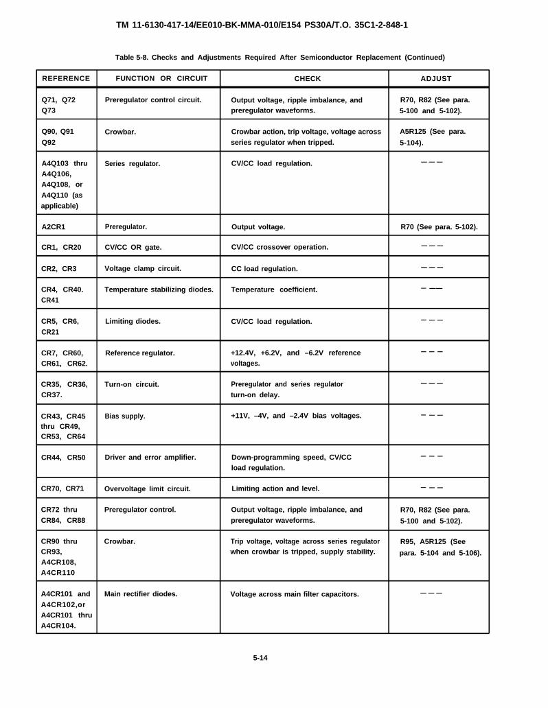
TM 11-6130-417-14/EE010-BK-MMA-010/E154 PS30A/T.O. 35C1-2-848-1
Table 5-8. Checks and Adjustments Required After Semiconductor Replacement (Continued)
REFERENCE FUNCTION OR CIRCUIT CHECK ADJUST
Q71, Q72 Preregulator control circuit. Output voltage, ripple imbalance, and R70, R82 (See para.Q73 preregulator waveforms. 5-100 and 5-102).
Q90, Q91 Crowbar. Crowbar action, trip voltage, voltage across A5R125 (See para.
Q92 series regulator when tripped. 5-104).
A4Q103 thru Series regulator. CV/CC load regulation. — — —
A4Q106,A4Q108, orA4Q110 (asapplicable)
A2CR1 Preregulator. Output voltage. R70 (See para. 5-102).
CR1, CR20 CV/CC OR gate. CV/CC crossover operation. — — —
CR2, CR3 Voltage clamp circuit. CC load regulation. — — —
CR4, CR40. Temperature stabilizing diodes. Temperature coefficient. — ——
CR41
CR5, CR6, Limiting diodes. CV/CC load regulation. — — —
CR21
CR7, CR60, Reference regulator. +12.4V, +6.2V, and –6.2V reference — — —
CR61, CR62. voltages.
CR35, CR36, Turn-on circuit. Preregulator and series regulator — — —
CR37. turn-on delay.
CR43, CR45 Bias supply. +11V, –4V, and –2.4V bias voltages. — — —
thru CR49,CR53, CR64
CR44, CR50 Driver and error amplifier. Down-programming speed, CV/CC — — —
load regulation.
CR70, CR71 Overvoltage limit circuit. Limiting action and level. — — —
CR72 thru Preregulator control. Output voltage, ripple imbalance, and R70, R82 (See para.CR84, CR88 preregulator waveforms. 5-100 and 5-102).
CR90 thru Crowbar. Trip voltage, voltage across series regulator R95, A5R125 (SeeCR93, when crowbar is tripped, supply stability. para. 5-104 and 5-106).A4CR108,A4CR110
A4CR101 and Main rectifier diodes. Voltage across main filter capacitors. — — —
A4CR102,orA4CR101 thruA4CR104.
5-14
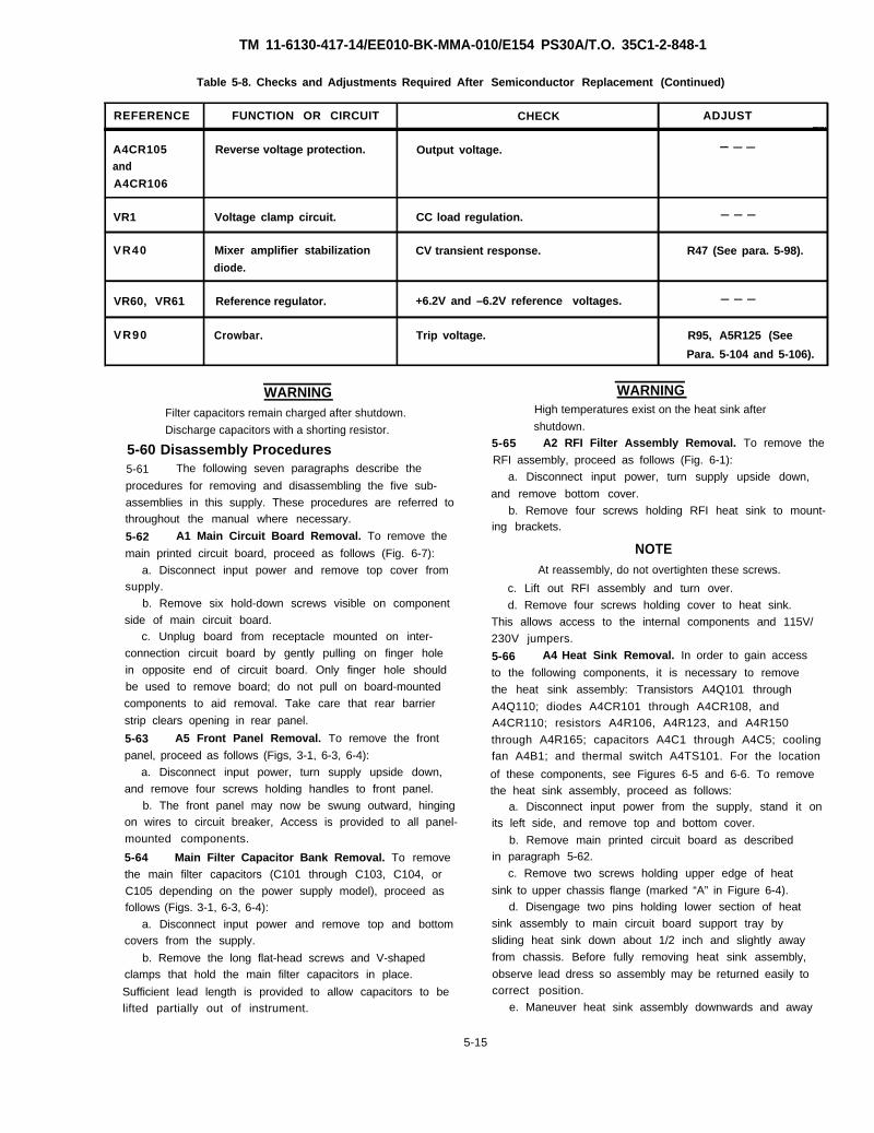
TM 11-6130-417-14/EE010-BK-MMA-010/E154 PS30A/T.O. 35C1-2-848-1
Table 5-8. Checks and Adjustments Required After Semiconductor Replacement (Continued)
REFERENCE FUNCTION OR CIRCUIT CHECK ADJUST
A4CR105 Reverse voltage protection. Output voltage. — — —
and
A4CR106
VR1 Voltage clamp circuit. CC load regulation. — — —
VR40 Mixer amplifier stabilization CV transient response. R47 (See para. 5-98).diode.
VR60, VR61 Reference regulator. +6.2V and –6.2V reference voltages. — — —
VR90 Crowbar. Trip voltage. R95, A5R125 (See
Para. 5-104 and 5-106).
WARNING WARNING
Filter capacitors remain charged after shutdown. High temperatures exist on the heat sink after
Discharge capacitors with a shorting resistor. shutdown.
5-60 Disassembly Procedures5-61 The following seven paragraphs describe the
procedures for removing and disassembling the five sub-
assemblies in this supply. These procedures are referred tothroughout the manual where necessary.
5-62 A1 Main Circuit Board Removal. To remove the
main printed circuit board, proceed as follows (Fig. 6-7):
a. Disconnect input power and remove top cover fromsupply.
b. Remove six hold-down screws visible on component
side of main circuit board.c. Unplug board from receptacle mounted on inter-
connection circuit board by gently pulling on finger hole
in opposite end of circuit board. Only finger hole should
be used to remove board; do not pull on board-mounted
components to aid removal. Take care that rear barrier
strip clears opening in rear panel.
5-63 A5 Front Panel Removal. To remove the front
panel, proceed as follows (Figs, 3-1, 6-3, 6-4):
a. Disconnect input power, turn supply upside down,
and remove four screws holding handles to front panel.
b. The front panel may now be swung outward, hingingon wires to circuit breaker, Access is provided to all panel-
mounted components.
5-64 Main Filter Capacitor Bank Removal. To remove
the main filter capacitors (C101 through C103, C104, or
C105 depending on the power supply model), proceed asfollows (Figs. 3-1, 6-3, 6-4):
a. Disconnect input power and remove top and bottomcovers from the supply.
b. Remove the long flat-head screws and V-shapedclamps that hold the main filter capacitors in place.
Sufficient lead length is provided to allow capacitors to belifted partially out of instrument.
5-65 A2 RFI Filter Assembly Removal. To remove the
RFI assembly, proceed as follows (Fig. 6-1):
a. Disconnect input power, turn supply upside down,
and remove bottom cover.
b. Remove four screws holding RFI heat sink to mount-ing brackets.
NOTEAt reassembly, do not overtighten these screws.
c. Lift out RFI assembly and turn over.
d. Remove four screws holding cover to heat sink.
This allows access to the internal components and 115V/
230V jumpers.
5-66 A4 Heat Sink Removal. In order to gain access
to the following components, it is necessary to remove
the heat sink assembly: Transistors A4Q101 through
A4Q110; diodes A4CR101 through A4CR108, andA4CR110; resistors A4R106, A4R123, and A4R150
through A4R165; capacitors A4C1 through A4C5; coolingfan A4B1; and thermal switch A4TS101. For the location
of these components, see Figures 6-5 and 6-6. To removethe heat sink assembly, proceed as follows:
a. Disconnect input power from the supply, stand it onits left side, and remove top and bottom cover.
b. Remove main printed circuit board as describedin paragraph 5-62.
c. Remove two screws holding upper edge of heat
sink to upper chassis flange (marked “A” in Figure 6-4).d. Disengage two pins holding lower section of heat
sink assembly to main circuit board support tray by
sliding heat sink down about 1/2 inch and slightly away
from chassis. Before fully removing heat sink assembly,
observe lead dress so assembly may be returned easily tocorrect position.
e. Maneuver heat sink assembly downwards and away
5-15
TM 11-6130-417-14/EE010-BK-MMA-010/E154 PS30A/T.O. 35C1-2-848-1
from chassis until it is resting on table (sufficient lead
Iength is provided). Gentle leverage with a thin screw-
driver may be necessary to allow heat sink assembly to
clear upper chassis flange. Access is now provided to all
components mounted on heat sink except resistors A4R150
through A4R165, and A4R123.
5-67 A4 Heat Sink Disassembly. To gain access to
resistors A4R123 and A4R150 through A4R165, it is
necessary to disassemble the heat sink assembly as
follows (Figs. 6-3 through 6-6):
a. Remove heat sink assembly as described in paragraph
5-66 above.
b. Turn supply upside down and place heat sink
assembly partially into chassis so fan (A4B1) is protruding
above chassis.
c. Remove four nuts and four shoulder washers
attaching fan mounting plate to heat sink. Do not remove
fan from mounting plate. When reassembling heat sink,
do not overtighten these screws. Too much tension willdamage the insulating rods.
d. Remove two screws holding current sampling
resistor A4R123 to heat sink. If necessary, the resistor
may be unsoldered at this point.
e. Remove mounting nuts from A4CR106 (and
A4CR107) on left side of heat sink, and from A4CR108
on right side of heat sink. Remove mounting nuts, bolts
and shoulder washers from transistor A4Q102 on right
side of heat sink (see Figure 7-5).
f. Slide this section of heat sink forward and off
insulating rods.
g. Remove four screws holding emitter resistor circuit
board to adjoining heat sink section. Access is now provided
to series regulator emitter resistors A4R150 through
A4R165 (see Figure FO-2).h. To remove emitter resistor circuit board completely,
unsolder connections to board, marking wires to permit
proper replacement.
5-68 A3 Interconnection Circuit Board Removal. To re-
place capacitor A3C3 or transformer A3T2, (shown in Figure 6-2),
it ia necessary to remove the interconnection circuit board. Per-
form the following procedure:
a. Remove main circuit board, RFI assembly, and heat sink as-
sembly as described in paragraphs 5-62, 5-65, and 5-66 (see Fig.
6-1 and Figs. 6-4 through 6-7).b. Remove six screws holding back panel to chassis
frame.
c. Stand supply on left side, and remove two screws
holding main circuit board support tray to back panel.
Move panel away from frame.
d. Remove two screws holding main circuit board
support tray to internal chassis divider.
e. Working from top rear of supply, interconnection
circuit board (still attached to main circuit board support
tray) can be angled up enough to allow access.
f. If necessary to completely remove interconnection
circuit board, remove two screws holding board to support
tray, one screw holding A3C3 capacitor clamp to support
tray, and two screws holding bias transformer A3T2 to
support tray. Unsolder connections to board, marking wires
to enable correct replacement, and remove board.
5 - 6 9 R E P A I R A N D R E P L A C E M E N T
5-70 The RPSTL for this manual contains a Iist of replaceable
parts. After replacing a semiconductor device, refer to Table 5-6
for checks and adjustments that may be necessary. All compo-
nents listed in Table 5-8 without A-designators are on the A1 main
printed circuit board.
5-71 ADJUSTMENT AND CALIBRATION
5-72 Adjustment and calibration may be required after
performance testing, troubleshooting, or repair and replace-ment. Perform only those adjustments that affect the
operation of the faulty circuit.
5-73 Meter Zero Adjustment
5-74 The meter pointer must rest on the zero calibrationmark on the meter scale when the instrument is at normal
operating temperature, resting in its normal operating
position, and turned off. To zero the meter proceed as
follows:
a. Connect load resistor of value shown in Figure 5-1,
turn on instrument, and allow it to come up to normal
operating temperature (about 30 minutes).
b. Turn instrument off and wait two minutes for power
supply capacitors to discharge completely.
c. Insert pointed object (pen point or awl) into small
indentation near top of round black plastic disc located
directly beIow meter face.d. Rotate plastic disc clockwise until meter reads zero,
then rotate counterclockwise slightly in order to free
adjustment screw from meter suspension. Pointer should
not move during latter part of adjustment.
5-75
5-76
Voltmeter Calibration(Figs. 3-1, 6-7)
To calibrate the voltmeter, proceed as follows:
a. Connect digital voltmeter across plus and minus
output terminals of supply, observing correct polarity.
b. Turn on supply and adjust VOLTAGE controls until
digital voltmeter reads exactly the maximum rated output
voltage.
c. Adjust R106 until front panel voltmeter also
5-16
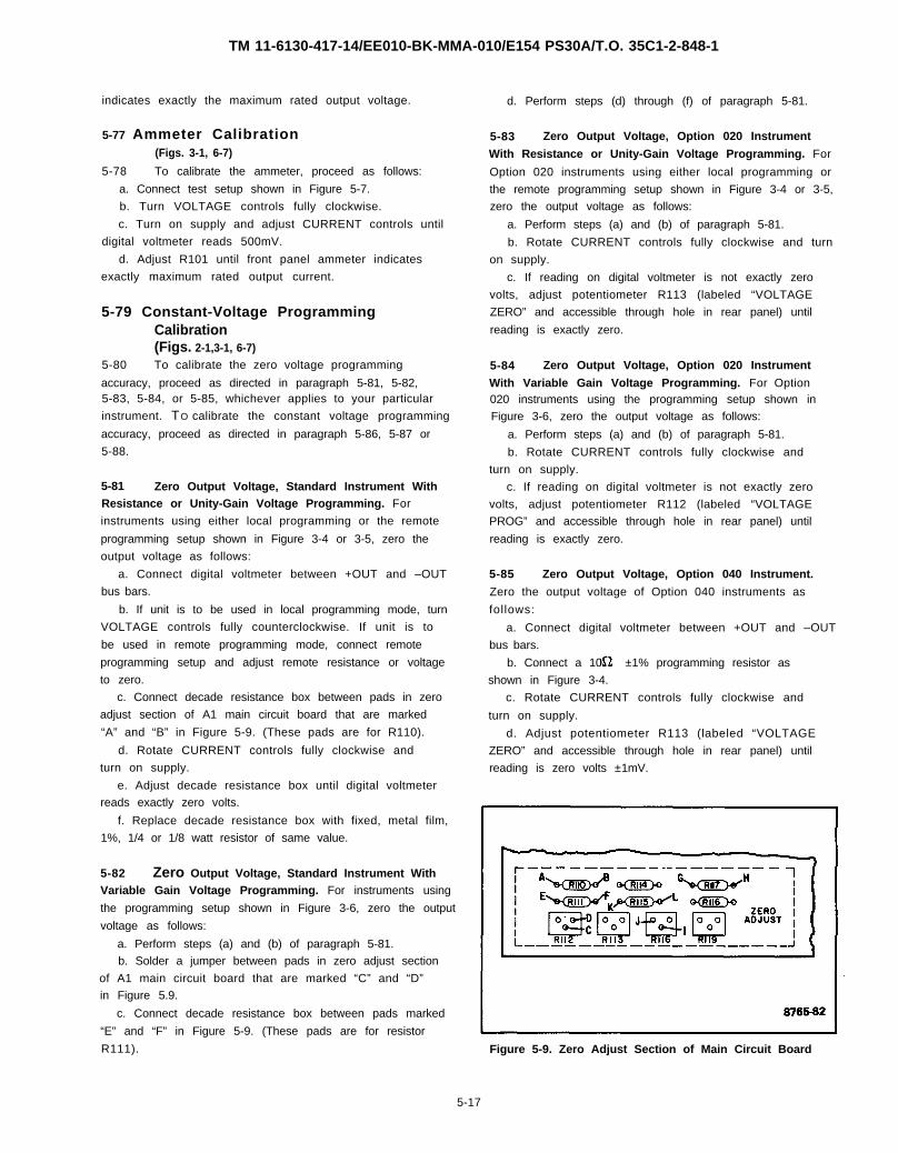
TM 11-6130-417-14/EE010-BK-MMA-010/E154 PS30A/T.O. 35C1-2-848-1
indicates exactly the maximum rated output voltage.
5-77 Ammeter Calibration(Figs. 3-1, 6-7)
5-78 To calibrate the ammeter, proceed as follows:
a. Connect test setup shown in Figure 5-7.
b. Turn VOLTAGE controls fully clockwise.
c. Turn on supply and adjust CURRENT controls until
digital voltmeter reads 500mV.
d. Adjust R101 until front panel ammeter indicates
exactly maximum rated output current.
5-79 Constant-Voltage ProgrammingCalibration(Figs. 2-1,3-1, 6-7)
5-80 To calibrate the zero voltage programming
accuracy, proceed as directed in paragraph 5-81, 5-82,5-83, 5-84, or 5-85, whichever applies to your particular
instrument. TO calibrate the constant voltage programming
accuracy, proceed as directed in paragraph 5-86, 5-87 or
5-88.
5-81 Zero Output Voltage, Standard Instrument WithResistance or Unity-Gain Voltage Programming. For
instruments using either local programming or the remote
programming setup shown in Figure 3-4 or 3-5, zero the
output voltage as follows:
a. Connect digital voltmeter between +OUT and –OUT
bus bars.
b. If unit is to be used in local programming mode, turn
VOLTAGE controls fully counterclockwise. If unit is to
be used in remote programming mode, connect remote
programming setup and adjust remote resistance or voltage
to zero.
c. Connect decade resistance box between pads in zero
adjust section of A1 main circuit board that are marked
“A” and “B” in Figure 5-9. (These pads are for R110).
d. Rotate CURRENT controls fully clockwise and
turn on supply.
e. Adjust decade resistance box until digital voltmeter
reads exactly zero volts.
f. Replace decade resistance box with fixed, metal film,
1%, 1/4 or 1/8 watt resistor of same value.
5-82 Zero Output Voltage, Standard Instrument WithVariable Gain Voltage Programming. For instruments using
the programming setup shown in Figure 3-6, zero the output
voltage as follows:
a. Perform steps (a) and (b) of paragraph 5-81.
b. Solder a jumper between pads in zero adjust section
of A1 main circuit board that are marked “C” and “D”
in Figure 5.9.
c. Connect decade resistance box between pads marked
“E” and “F” in Figure 5-9. (These pads are for resistor
d. Perform steps (d) through (f) of paragraph 5-81.
5-83 Zero Output Voltage, Option 020 Instrument
With Resistance or Unity-Gain Voltage Programming. For
Option 020 instruments using either local programming or
the remote programming setup shown in Figure 3-4 or 3-5,
zero the output voltage as follows:
a. Perform steps (a) and (b) of paragraph 5-81.
b. Rotate CURRENT controls fully clockwise and turn
on supply.
c. If reading on digital voltmeter is not exactly zero
volts, adjust potentiometer R113 (labeled “VOLTAGE
ZERO” and accessible through hole in rear panel) until
reading is exactly zero.
5-84 Zero Output Voltage, Option 020 Instrument
With Variable Gain Voltage Programming. For Option020 instruments using the programming setup shown in
Figure 3-6, zero the output voltage as follows:
a. Perform steps (a) and (b) of paragraph 5-81.
b. Rotate CURRENT controls fully clockwise and
turn on supply.
c. If reading on digital voltmeter is not exactly zero
volts, adjust potentiometer R112 (labeled “VOLTAGE
PROG” and accessible through hole in rear panel) until
reading is exactly zero.
5-85 Zero Output Voltage, Option 040 Instrument.
Zero the output voltage of Option 040 instruments as
follows:
a. Connect digital voltmeter between +OUT and –OUT
bus bars.
b. Connect a 10 ±1% programming resistor as
shown in Figure 3-4.
c. Rotate CURRENT controls fully clockwise and
turn on supply.
d. Adjust potentiometer R113 (labeled “VOLTAGE
ZERO” and accessible through hole in rear panel) until
reading is zero volts ±1mV.
R111). Figure 5-9. Zero Adjust Section of Main Circuit Board
5-17
TM 11-6130-417-14/EE010-BK-MMA-010/E154 PS30A/T.O. 35C1-2-848-1
5-92 Zero Output Current, Standard InstrumentWith Variable Gain Voltage Programming. For instruments
using the remote programming setup shown in Figure 3-9,
zero the output current as follows:
a. Perform steps (a) and (b) of paragraph 5-91.
b. Solder a jumper between pads in zero adjust section
of A1 main circuit board that are marked “l” and “J” inFigure 5-9.
c. Connect decade resistance box between pads marked
“K” and “L” in Figure 5-9. (These pads are for R115.)
d. Perform steps (d) through (f) of paragraph 5-91.
5-93 Zero Output Current, Option 021 InstrumentWith Resistance or Fixed Gain Voltage Programming.For Option 021 instruments using either local program-
ming or the remote programming setup shown in Figure
3-7 or 3-8, zero the output current as follows:
a. Perform steps (a) and (b) of paragraph 5-91.
b. Rotate VOLTAGE controls fully clockwise and
turn on supply.
c. If reading on digital voltmeter is not exactly zero
volts, adjust potentiometer R119 (labeled “CURRENT
ZERO” and accessible through hole in rear panel) until
reading is exactly zero.
5-94 Zero Output Current, Option 021 Instrument
With Variable Gain Voltage Programming. For Option 021
instruments using the programming setup shown in Figure
3-9, zero the output current as follows:
a. Perform steps (a) and (b) of paragraph 5-91.
b. Rotate VOLTAGE controls fully clockwise and
turn on supply.
c. If reading on digital voltmeter is not exactly zerovolts, adjust potentiometer R116 (labeled “CURRENT
PROG” and accessible through hole in rear panel) until
reading is exactly zero.
5-95 Zero Output Current, Option 040 Instrument.Zero the output current of Option 040 instruments as
follows:
a. Connect test setup shown in Figure 5-7, except omit
load resistor RL and connect just current sampling resistor
R S across the output of the supply.
b. Connect remote programming setup shown in Figure
3-7 and adjust remote resistance to zero.
c. Rotate VOLTAGE controls fully clockwise and turn
on supply.
d. If reading on digital voltmeter is not exactly zerovolts, adjust potentiometer R119 (labeled “CURRENT
ZERO” and accessible through hole in rear panel) until
reading is zero volts ±2mV.
5-96 Constant-Current Programming Accuracy,Standard Instrument. To calibrate the constant-currentprogramming current of a standard instrument, proceed
as follows:
a. Connect test setup shown in Figure 5-7.
b. Disconnect strap between terminals A5 and A6 on
rear barrier strip.
c. Connect 0.1%, 1/8 watt resistor of value shown
below between terminals A4 and A6 on rear barrier strip.Model Value
6259B 2 0 0
6260B 2 0 0
6261B 2 0 0
6268B 1 8 0
6269B 2 0 0
d. Connect decade resistance box in place of R30 (mount-
ed on standoffs on main circuit board; see Figure 7-7).
e. Rotate VOLTAGE controls fully clockwise and
turn on supply.f. Adjust decade resistance box until digital voltmeter
indicates exactly 0.5Vdc.
g. Replace decade resistance box with fixed, composi-
tion, 5%, 1/2 watt resistor of same value.
5-97 Constant-Current Programming Accuracy, Option021 or Option 040 Instrument. To calibrate the constant-
current programming current of an Option 021 or Option
040 instrument, proceed as follows:a. Perform steps (a) through (c) of paragraph 5-96.
b. Rotate VOLTAGE controls fully clockwise and
turn on supply.
c. Adjust potentiometer R116 (labeled “CURRENT
PROG” and accessible through hole in rear panel) until
digital voltmeter indicates 0.5Vdc ±10mV.
5-98 Load Transient Recovery Time Adjustment(Figs. 3-1, 6-7)
5-99 To adjust the transient response, proceed as
follows:
a. Connect test setup shown in Figure 5-4.
b. Repeat steps (a) through (k) as outlined in paragraph
5-30.
c. Adjust R47 until transient response to within
specification as shown in Figure 5-5.
5-100 Ripple Balance Adjustment(Figs. 3-1, 6-7)
5-101 This procedure ensures balanced triac operation by en-
suring that its conduction time is within 25% of being equal in both
directions. To check for imbalance, proceed as follows:
a. Connect load resistor specified in Figure 5-1 across rear out-
put terminals of supply (Fig. 2-1).
b. Connect variable autotransformer between input power
source and power supply input and adjust it for a 115 Vac input to
the supply.
c. connect ac-coupled oscilloscope across series regulator (be-
tween *TP102 and *TP103) (Fig. FO-1).*Test points are identified on schematic only.
5-19

TM 11-6130-417-14/EE010-BK-MMA-010/E154 PS30A/T.O. 35C1-2-848-1
5-92 Zero Output Current, Standard InstrumentWith Variable Gain Voltage Programming. For instruments
using the remote programming setup shown in Figure 3-9,
zero the output current as follows:
a. Perform steps (a) and (b) of paragraph 5-91.
b. Solder a jumper between pads in zero adjust section
of A1 main circuit board that are marked “l” and “J” inFigure 5-9.
c. Connect decade resistance box between pads marked
“K” and “L” in Figure 5-9. (These pads are for R115.)
d. Perform steps (d) through (f) of paragraph 5-91.
5-83 Zero Output Current, Option 021 InstrumentWith Resistance or Fixed Gain Voltage Programming.For Option 021 instruments using either local program-
ming or the remote programming setup shown in Figure
3-7 or 3-8, zero the output current as follows:
a. Perform steps (a) and (b) of paragraph 5-91.
b. Rotate VOLTAGE controls fully clockwise and
turn on supply.
c. If reading on digital voltmeter is not exactly zero
volts, adjust potentiometer R119 (labeled “CURRENT
ZERO” and accessible through hole in rear panel) until
reading is exactly zero.
5-94 Zero Output Current, Option 021 Instrument
With Variable Gain Voltage Programming. For Option 021
instruments using the programming setup shown in Figure
3-9, zero the output current as follows:
a. Perform steps (a) and (b) of paragraph 5-91.
b. Rotate VOLTAGE controls fully clockwise and
turn on supply.
c. If reading on digital voltmeter is not exactly zerovolts, adjust potentiometer R116 (labeled “CURRENT
PROG” and accessible through hole in rear panel) until
reading is exactly zero.
5-95 Zero Output Current, Option 040 Instrument.Zero the output current of Option 040 instruments as
follows:
a. Connect test setup shown in Figure 5-7, except omit
load resistor RL and connect just current sampling resistor
R S across the output of the supply.
b. Connect remote programming setup shown in Figure
3-7 and adjust remote resistance to zero.
c. Rotate VOLTAGE controls fully clockwise and turn
on supply.
d. If reading on digital voltmeter is not exactly zerovolts, adjust potentiometer R119 (labeled “CURRENT
ZERO” and accessible through hole in rear panel) until
reading is zero volts ±2mV.
5-96 Constant-Current Programming Accuracy,Standard Instrument. To calibrate the constant-currentprogramming current of a standard instrument, proceed
as follows:
a. Connect test setup shown in Figure 5-7.
b. Disconnect strap between terminals A5 and A6 on
rear barrier strip.
c. Connect 0.1%, 1/8 watt resistor of value shown
below between terminals A4 and A6 on rear barrier strip.Model Value
6259B 2 0 0
6260B 2 0 0
6261B 2 0 0
6268B 1 8 0
6269B 2 0 0
d. Connect decade resistance box in place of R30 (mount-
ed on standoffs on main circuit board; see Figure 7-7).
e. Rotate VOLTAGE controls fully clockwise and
turn on supply.f. Adjust decade resistance box until digital voltmeter
indicates exactly 0.5Vdc.
g. Replace decade resistance box with fixed, composi-
tion, 5%, 1/2 watt resistor of same value.
5-97 Constant-Current Programming Accuracy, Option021 or Option 040 Instrument. To calibrate the constant-
current programming current of an Option 021 or Option
040 instrument, proceed as follows:a. Perform steps (a) through (c) of paragraph 5-96.
b. Rotate VOLTAGE controls fully clockwise and
turn on supply.
c. Adjust potentiometer R116 (labeled “CURRENT
PROG” and accessible through hole in rear panel) until
digital voltmeter indicates 0.5Vdc ±10mV.
5-98 Load Transient Recovery Time Adjustment(Figs. 3-1, 6-7)
5-99 To adjust the transient response, proceed as
follows:
a. Connect test setup shown in Figure 5-4.
b. Repeat steps (a) through (k) as outlined in paragraph
5-30.
c. Adjust R47 until transient response to within
specification as shown in Figure 5-5.
5-100 Ripple Balance Adjustment(Figs. 3-1, 6-7)
5-101 This procedure ensures balanced triac operation by en-
suring that its conduction time is within 25% of being equal in both
directions. To check for imbalance, proceed as follows:
a. Connect load resistor specified in Figure 5-1 across rear out-
put terminals of supply (Fig. 2-1).
b. Connect variable autotransformer between input power
source and power supply input and adjust it for a 115 Vac input to
the supply.
c. connect ac-coupled oscilloscope across series regulator (be-
tween *TP102 and *TP103) (Fig. FO-1).*Test points are identified on schematic only.
5-19
TM 11-6130-417-14/EE010-BK-MMA-010/E154 PS30A/T.O. 35C1-2-848-1
d. Turn CURRENT controls fully clockwise, turn on
supply, and adjust VOLTAGE controls for maximum
rated output voltage.
e. Adjust oscilloscope to observe 120Hz sawtooth
waveform. Peak amplitudes of adjacent sawtooth peaks
should be within 25% of each other.
f. If amplitude difference is greater than 25%, turn off
supply and replace R82 with decade resistance.
g. Turn on supply and adjust decade resistance toreduce imbalance to within 25%.
h. Vary input Iine voltage from 100 to 130 Vac and insure that
excessive imbalance does not exist anywhere within this range.
Replace decade box with equivalent resistor.
5-104 Crowbar Trip Voltage Adjustment(Figs. 3-1, 6-3)
5-105 To adjust the voltage at which the crowbar fires,
proceed as follows:
a. Turn front panel OVERVOLTAGE ADJUST
potentiometer A5R125 fully clockwise.
b. Turn on supply.
c. Set output voltage to desired trip voltage.
d. Turn A5R125 slowly counterclockwise until thecrowbar fires (amber OVERVOLTAGE lamp lights and
voltmeter indication falls to zero).
e. Turn off supply and turn down output voltage controls.
f. Turn on supply and set desired output voltage.
NOTENOTE
If imbalance cannot be reduced to within
25%, check capacitors C70 and C72, and
diodes CR79 through CR84. If thesecomponents test satisfactorily, the problem
may be due to distortion present on the
ac power line.
5-102 Preregulator Tracking Adjustment(Figs. 3-1, 6-7)
5-103 To adjust the voltage drop across the series regulator,proceed as follows:
a. Connect load resistor specified in Figure 5-1 across rear out-
put terminals of supply.
b. Connect variable autotransformer between input power
source and power supply input and adjust it for a 115Vac input tothe supply.
c. Connect dc voltmeter across series regulator (betweenTP102 and TP103) (Fig. FO-1).
d. Turn CURRENT controls fully clockwise.
e. To check voltage drop across regulator at low output
voltage, short circuit the load resistor and adjust VOLTAGE
controls for maximum rated output current on front panel
ammeter.f. Adjust R70 (RAMP ADJ.) until voltmeter reads
3.5 ±0.3Vdc.
g. To check the voltage drop at high output voltage,
remove short circuit from across load resistor and adjust
VOLTAGE controls for maximum rated output current.Voltmeter reading should again be 3.5 ±0.3Vdc.
h. Vary input line voltage from 100 to 130Vac. Voltmeter read-
ing should vary between 3.2 and 3.8Vdc. If reading exceeds this
range, proceed to step (i).
i. Replace R77 with decade box. Vary input line voltage be-
tween 100 to 130Vac and adjust decade box until voltmeter read-
ing variation is minimal and within range of 3.2 to 3.8Vdc. Replace
decade box with equivalent resistor.
It is recommended that the cro wbar trip volt-
age be set higher than the normal output volt-age by no less than 5% of the output voltageplus 2 volts for the Models 6259B, 6260B,
or 6261B, or 5% of the output voltage plus
one volt for the Models 6268B or 6269B. If an
occasional tripping of the crowbar can be
tolerated as a load is being disconnected, thecrowbar trip point can be set much closer to
the operating voltage of the supply.
5-106 Maximum Crowbar Trip Voltage Adjustment(Figs. 3-1, 6-3, 6-7, FO-1)
5-107 To adjust the maximum voltage at which the
crowbar fires, proceed as follows:
a. Rotate A5R125 (OVERVOLTAGE ADJUST) and
CURRENT controls fully clockwise.
b. Disconnect one end of R72 (at TP70 or TP71) to
temporarily disable the overvoltage limit circuit.c. Connect decade resistance box in place of R95
(mounted on standoffs on main circuit board).
d. Turn on supply and adjust VOLTAGE controls for
output voltage shown below:Model Value
6259B 12Vdc
6260B 12Vdc
6261B 23Vdc
6268B 45Vdc
6269B 45Vdc
e. Adjust decade resistance box until crowbar fires.
f. Replace decade resistance with appropriate value
resistor in R95 position and reconnect resistor R72. Maxi-
mum crowbar trip voltage is now set at voltage given in step (d).
5-108 Disabling the Crowbar(Figs. 6-7, FO-1)
5-109 To disable the crowbar completely, disconnect
either end of R98 at TP96 or TP97 on the main circuit board.
5-20
TM 11-6130-417-14/EE010-BK-MMA-010/E154 PS30A/T.O. 35C1-2-848-1
5-110
5-111
OVERHAUL AND REBUILD
The following instructions set forth the procedures forcompletely disassembling the supply for overhaul or rebuild tasks.Before beginning these tasks, the supply is tested to determinewhether or not the unit is serviceable. Malfunctions should benoted during the test and the parts responsible should be replacedduring the reassembly procedures.
5-112
5-113
COMPLETE REMOVAL OF A3 lNTERCON-NECTION BOARD(Figs. 6-1 through 6-6, FO-3)
To partially remove the A3 interconnection board, the A1main circuit board, A2RFI assembly and A4 heat sink assemblymust first be fully or partially removed, as prescribed in paragraph5-68, steps a. through e. The following instructions set forth stepsfor A3 board removal to a stage where the A3 interconnectionboard and the A4 heat sink can be removed as an entity (to avoidneed for some unsoldering). The two assemblies can then be sep-arated by unsoldering the leads while on the bench, if necessary.
a. Move heat sink A4 out of chassis according to paragraph5-66.
b. Tag and unsolder leads to primary side of bias transformerA3TR.
c. Move A2 RFI assembly out of chassis according to para-graph 5-65.
d. Move heat aink A4 and A2 RFI assembly as an entity to thebench.
e. If the two units must be separated, then unsolder the leadsfrom the unit of interest.
f. Remove screw that secures A3C3 capacitor clamp to maincircuit board support tray.
g. Remove two screws that secure bias transformer A3T2 tomain circuit board support tray.
h. At A3 board, tag and unsolder leads that run to A5 panel.i. Tag and disconnect the heavy leads from A4 heat sink.j. Remove A3 board and A4 heat sink together, or tag and un-
solder the leads between the two assemblies and move the as-sembly (intended to be completely removed) to the bench.
k. Move main circuit board tray to bench.l. Separate A3 board from A4 heat sink by tagging and unsold-
ering leads, if necessary.m. Remove grommet from main circuit board support tray, if
necessary.
5-114 COMPLETE REMOVAL OF A4 HEAT SINK
5-115 The A4 heat sink is partially removed (with wiring stillconnected) from the chassis by following the procedure in para-graph 5-66. If the A4 heat sink is to be fully removed, it can beremoved together with the A3 interconnection board or removedseparately. Refer to paragraph 5-112 if A4 heat sink is to be fullyremoved.
5-116 POWER TRANSFORMER T1 REMOVAL(Figs. 6-3, 6-4, FO-3)
5-117 To remove the power transformer T1, perform the fol-lowing procedure:
a. Set chassis on its right side.b. Tag and unsolder leads from terminals on secondary side of
transformer T1.c. Tag and disconnect leads fastened to terminals 6 and 7 of
primary power transformer T1.d. Remove four mounting nuts and washers from T1. Lift trans-
former out though the top side of chassis and move to bench.
5-118 B2 FAN REMOVAL(Figs. 6-2 through 6-4, FO-3)
5-119 To remove fan B2, the A3 interconnection board mustbe at least partially removed so that the fan leads of fan B2 canbe unsoldered from terminals of bias transformer A3T2.
a. Partially remove board A3 as per paragraph 5-68.b. Tag and unsolder two fan leads from terminals of bias trans-
former A3T2.c. Pull fan leads through hole in internal chassis divider.d. While holding fan, remove two screws and washers that se-
cure fan to bottom of circuit board tray.e. Move fan with its two brackets to bench.f. Remove two mounting brackets.
5-120 COMPLETE REMOVAL OF MAIN FILTERCAPACITOR BANK(Figs. 6-3, 6-4, FO-3)
5-121 To remove main filter capacitor bank, perform the follow-ing procedure:
a. Partially remove main filter capacitor bank as per paragraph5-64.
b. Remove screw and washers that secure cable clamp to inter-nal chassis divider. (Cable clamp is located next to capacitorbank.)
c. Tag and disconnect four cables to capacitor bank.d. Remove capacitor bank and move to bench.e. If a capacitor is to be separated from bank assembly, remove
two screws that secure the capacitor to the bus bars and movecapacitor to bench.
5-122 B BUS BARS (+B, –B) REMOVAL(Figs. 6-1, 6-2, 6-5, 6-6, FO-3)
5-123 To remove the +B and/or -B bus bar, it is necessaryto remove the filter assembly A2 RFI and heat sink A4, as de-scribed in paragraphs 5-65 and 5-66.
a. Tag and disconnect two leads that run inside chassis to A1main circuit board.
5-21
TM 11-6130-417-14/EE010-BK-MMA-010/E154 PS30A/T.O. 35C1-2-848-1
b. On +B bus bar (inside), tag and disconnect red lead thatruns to A3 interconnection board.
c. Tag and remove capacitor C19 from between the two busbars.
d. Tag and disconnect heavy black lead from –B bus bar.e. Remove two screws and nylon shoulder washers that secure
bus bar to rear panel.f. Move bus bar to bench.
5-124
5-125
REMOVAL OF STANDOFF MOUNTS FORA2 RFI CIRCUIT ASSEMBLY(Figs. 6-1, FO-3)
To gain access to the standoff supports for A2 RFI cir-cuit assembly, the A2 RFl assembly must be moved out of theway.
a. Remove two screws from rear panel that secure the standoffmount to the rear panel.
b. Move mount to bench.c. Remove two screws and nuts that secure front-end standoff
mount to the internal chassis divider.d. Move standoff mount to bench.
5-126 REMOVAL OF INPUT POWER TERMINALBOARD TB1(Figs. FO-1, FO-3)
5-127 To gain access to terminal board TB1, the rear panelmust be moved aside.
a. Remove cable strain relief assembly, if so equipped.b. Tag and disconnect two internal leads that are fastened to
terminal board.c. Remove two screws that secure terminal board to rear panel.d. Remove upper screw and nut of the ground terminal (middle
terminal) and move terminal board to bench.
5-128 REMOVAL OF REAR PANEL(Figs. 2-1, 6-9, FO-3)
5-129 To remove rear panel, all cables fastened to the two busbars and to the input terminal board TB1 must be disconnected.
a. Ensure that all cables are disconnected from bus bars andterminal board CB1. (Paragraphs 5-114, 5-119, and 5-122.)
b. Remove three screws and washers that secure rear panel toright side of chassis.
c. Remove three screws and washers that secure rear panel toleft side of chassis.
d. Remove panel from chassis and move to bench.e. If necessary, remove four rubber foot pads and binding post
from rear panel.
5-130 A5 FRONT PANEL REMOVAL(Figs. 6-3, 6-4)
5-131 The four screws that secure the two handles to thechassis frame also secure the front panel to the frame.
a. Set chassis on bench, bottom side down.b. Remove four screws and nuts that secure the two handles to
the frame.c. Move handles to bench and rotate front panel downward.
5-132 A5 FRONT PANEL DISASSEMBLY(Figs. 6-3, 6-4, 6-9, FO-3)
5-133 To disassemble the front panel, perform the followingprocedure:
a. Tag and disconnect leads to LINE circuit breaker A5CB1.b. Remove four screws that secure A5CB1 to front panel and
move A5CB1 to bench.c. Remove two knobs from VOLTAGE/COARSE/FINE poten-
tiometers A5R121 and A5R122.d. Remove two knobs from CURRENT/COARSE/FINE poten-
tiometers A5R123 and A5R124.e. Tag and unsolder leads to the four potentiometers A5R121,
A5R122, A5R123 and A5R124.f. Tag four potentiometers, remove hex nuts that secure four
potentiometers (steps d. and e.) to front panel, and move tobench.
g. Unsolder leads to OVERVOLTAGE ADJUST potentiometerA5R125.
h. With a wrench, turn (CCW) hex bushing mount of A5R125 toremove it.
i. Unsolder leads from OVERVOLTAGE indicating lamp A5DS2.j. Remove voltage and current meters A5M1 and A5M2.
(1) Unsolder two wires from meter.(2) On one side of meter (with a pointed tool), slightly pry out
bezel side tab so as to disengage it from the meter.
NOTE
Four meter mount compression springs will becomeexposed in the next step. Be careful not to losethese springs.
(3) An other side of meter, pry out bezel side tab so as todisengage it from meter.
(4) Move meter to bench.(5) Remove four meter mount compression springs from the
front side of the meter.
5-22
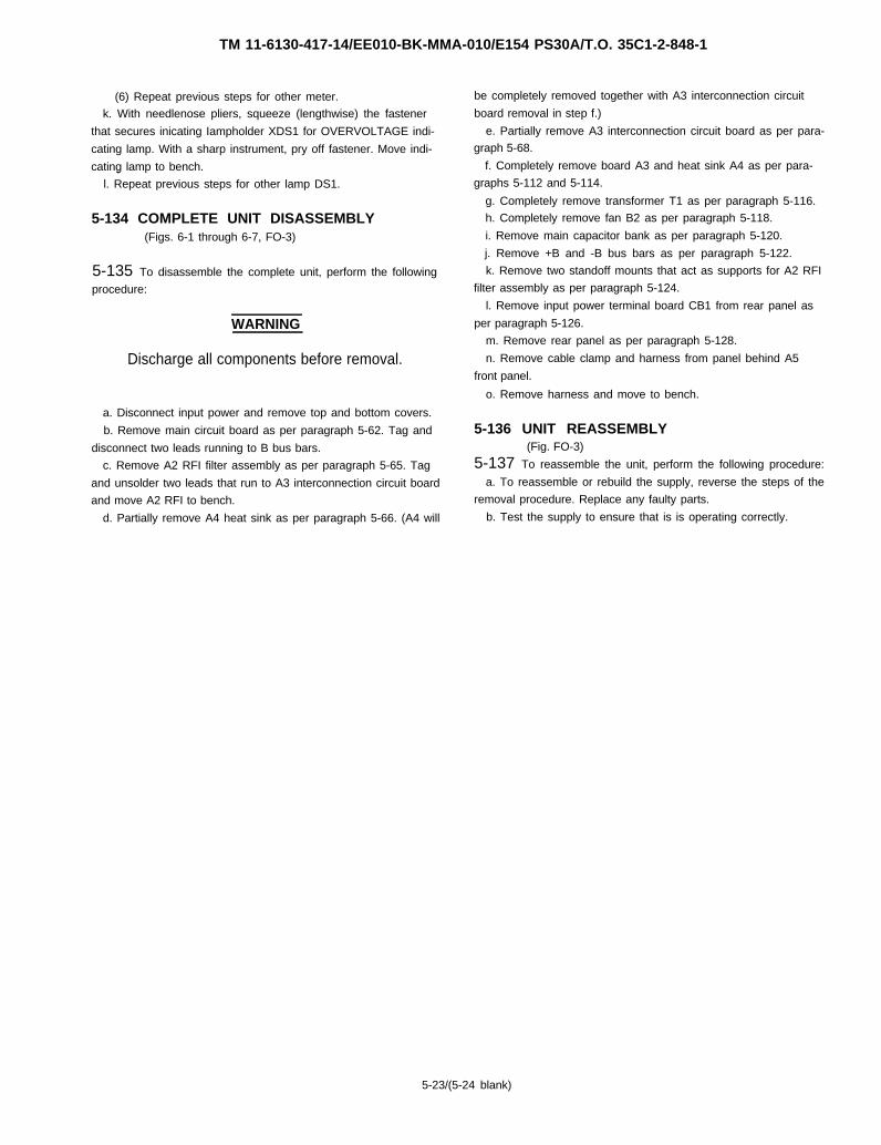
TM 11-6130-417-14/EE010-BK-MMA-010/E154 PS30A/T.O. 35C1-2-848-1
(6) Repeat previous steps for other meter.
k. With needlenose pliers, squeeze (lengthwise) the fastener
that secures inicating Iampholder XDS1 for OVERVOLTAGE indi-
cating lamp. With a sharp instrument, pry off fastener. Move indi-
cating lamp to bench..l. Repeat previous steps for other lamp DS1.
5-134 COMPLETE UNIT DISASSEMBLY(Figs. 6-1 through 6-7, FO-3)
5-135 To disassemble the complete unit, perform the following
procedure:
WARNING
Discharge all components before removal.
a. Disconnect input power and remove top and bottom covers.
b. Remove main circuit board as per paragraph 5-62. Tag and
disconnect two leads running to B bus bars.
c. Remove A2 RFI filter assembly as per paragraph 5-65. Tag
and unsolder two leads that run to A3 interconnection circuit board
and move A2 RFI to bench.
d. Partially remove A4 heat sink as per paragraph 5-66. (A4 will
be completely removed together with A3 interconnection circuit
board removal in step f.)
e. Partially remove A3 interconnection circuit board as per para-
graph 5-68.
f. Completely remove board A3 and heat sink A4 as per para-
graphs 5-112 and 5-114.
g. Completely remove transformer T1 as per paragraph 5-116.
h. Completely remove fan B2 as per paragraph 5-118.
i. Remove main capacitor bank as per paragraph 5-120.
j. Remove +B and -B bus bars as per paragraph 5-122.
k. Remove two standoff mounts that act as supports for A2 RFI
filter assembly as per paragraph 5-124.
l. Remove input power terminal board CB1 from rear panel as
per paragraph 5-126.
m. Remove rear panel as per paragraph 5-128.
n. Remove cable clamp and harness from panel behind A5
front panel.
o. Remove harness and move to bench.
5-136 UNIT REASSEMBLY(Fig. FO-3)
5-137 To reassemble the unit, perform the following procedure:
a. To reassemble or rebuild the supply, reverse the steps of the
removal procedure. Replace any faulty parts.
b. Test the supply to ensure that is is operating correctly.
5-23/(5-24 blank)

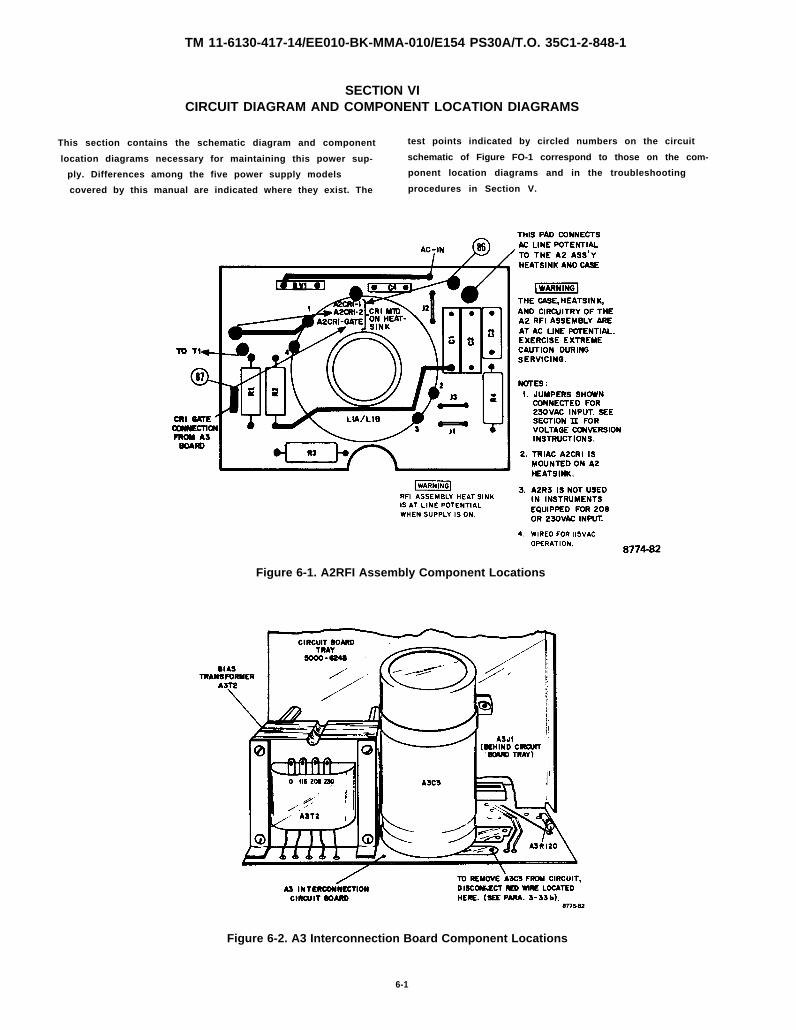
TM 11-6130-417-14/EE010-BK-MMA-010/E154 PS30A/T.O. 35C1-2-848-1
SECTION VICIRCUIT DIAGRAM AND COMPONENT LOCATION DIAGRAMS
This section contains the schematic diagram and component test points indicated by circled numbers on the circuit
location diagrams necessary for maintaining this power sup- schematic of Figure FO-1 correspond to those on the com-
ply. Differences among the five power supply models ponent location diagrams and in the troubleshooting
covered by this manual are indicated where they exist. The procedures in Section V.
Figure 6-1. A2RFI Assembly Component Locations
Figure 6-2. A3 Interconnection Board Component Locations
6-1
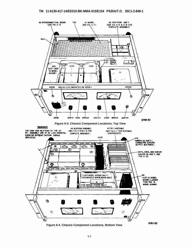
TM 11-6130-417-14/EE010-BK-MMA-010/E154 PS30A/T.O. 35C1-2-848-1
Figure 6-3. Chassis Component Locations, Top View
Figure 6-4. Chassis Component Locations, Bottom View
6-2
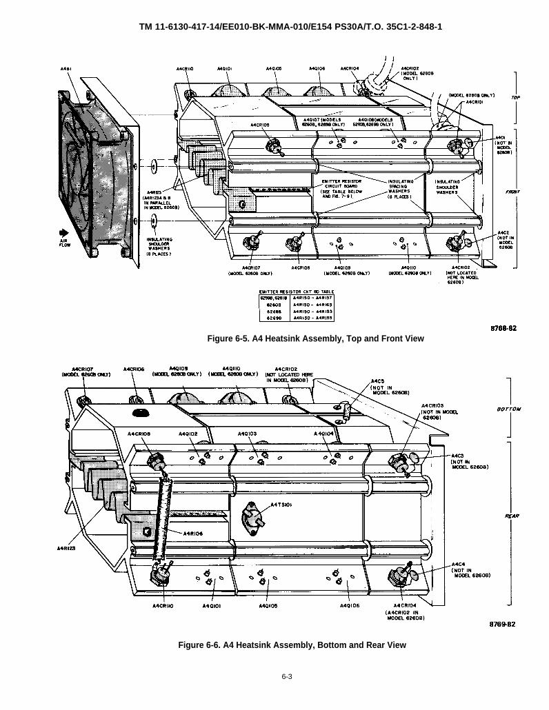
TM 11-6130-417-14/EE010-BK-MMA-010/E154 PS30A/T.O. 35C1-2-848-1
Figure 6-5. A4 Heatsink Assembly, Top and Front View
Figure 6-6. A4 Heatsink Assembly, Bottom and Rear View
6-3
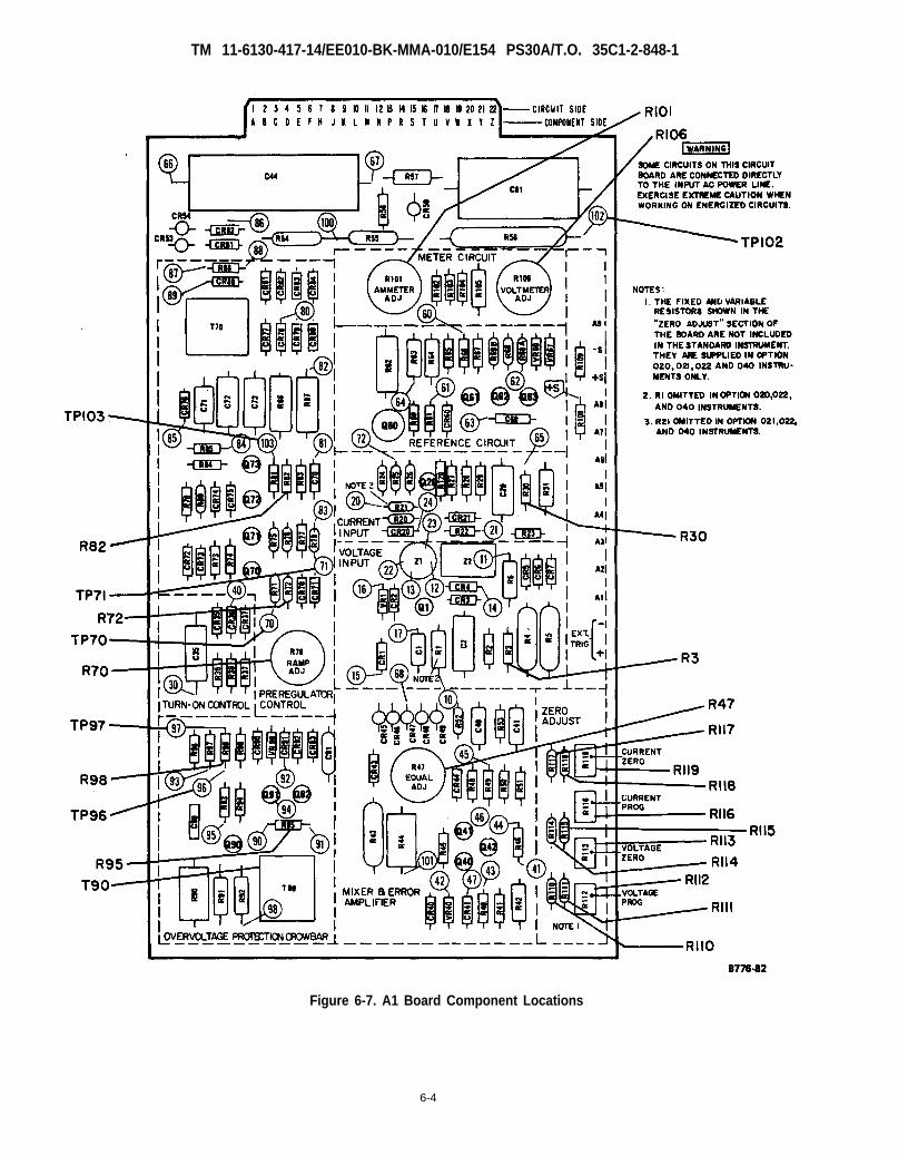
TM 11-6130-417-14/EE010-BK-MMA-010/E154 PS30A/T.O. 35C1-2-848-1
Figure 6-7. A1 Board Component Locations
6-4
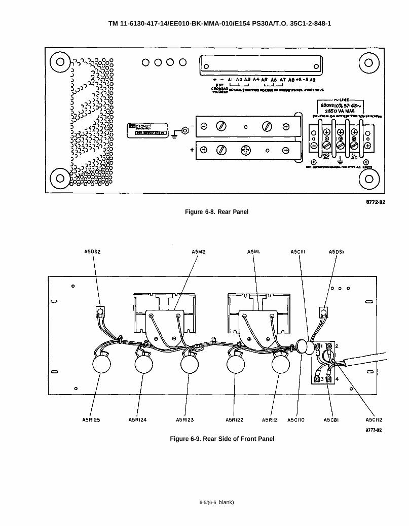
TM 11-6130-417-14/EE010-BK-MMA-010/E154 PS30A/T.O. 35C1-2-848-1
Figure 6-8. Rear Panel
Figure 6-9. Rear Side of Front Panel
6-5/(6-6 blank)

TM 11-6130-417-14/EE010-BK-MMA-010/E154 PS30A/T.O. 35C1-2-848-1
APPENDIX A
REFERENCES
AR 750-56
DA PAM 310-1
SB 11-573
TB S1G-22
TB 43-0116
TB 43-0116
TB 746-10
TB 38-750
TM 740-90-1
TM 750-244-2
TM 11-6625-1541-15
TM 11-6625-654-14
TM 11-6625-2568-14
TM 11-6625-2735-14
0969-LP-170-1090T.O. 33A1-13-496-1
Painting, Camouflage Painting and Marking of Army Material.
Consolidated Index of Army Publications and Blank Forms.
Painting and Preservation Supplies Available for Field Use for Electronics Command Equipment.
Solder and Soldering.
Identification of Radioactive Items in the Army Supply System.
Field Instructions for Painting and Preserving Electronics Command Equipment Including
Camouflage Pattern Painting of Electrical Equipment Shelters.
Field Instructions for Painting and Preserving Electronics Command Equipment.
The Army Maintenance Management System (TAMMS).
Administrative Storage of Equipment.
Procedures for Destruction of Electronics Materiel to Prevent Enemy Use (Electronics Command).
Operator, Organizational, Direct Support, General Support and Depot MaintenanceManual: Hewlett-Packard RMS Voltmeter Model 3400A.
Operator, Organizational, Direct Support, General Support, and Depot Maintenance ManualIncluding Repair Parts and Special Tool Lists for Multimeter AN/USM-223
Operator, Organizational, Direct Support, and General Support Maintenance Manual forOscilloscope AN/USM-261C (NSN 6625-00-106-9622).
Operator’s, Organizational, Direct Support, and General Support Maintenance Manual (IncludingDepot Maintenance) for Oscilloscope OS-261/U (NSN 6625-00-127-0079).
A-1/(A-2 blank)

TM 11-6130-417-14/EE010-BK-MMA-010/E154 PS30A/T.O. 35C1-2-848-1
APPENDIX B
MAINTENANCE ALLOCATION
Section I. INTRODUCTION
B-1. General. This appendix provides a summary of the
maintenance operations for the Regulated DC Power Supply
Model 6268B. It authorizes categories of maintenance for specific
maintenance functions on repairable items and components and
the tools and equipment required to perform each function.
B-2. Maintenance Concept. Two Ievels of maintenance
shall be utilized for the equipment as follows:
Organizational Level
Depot Level.
a. Organization Maintenance. That maintenance which is the
responsibility of and performed by a using organization on its
assigned equipment. Its phases normally consist of inspecting,
servicing, lubricating, and adjusting, and the replacement of parts,
minor assemblies and subassemblies. This level is designated by
an O in the Maintenance Category columns in Section II.
b. Depot Maintenance. That maintenance which is the
responsibility of and performed by designated maintenance
activities, to augment stocks of serviceable material, and to
support lower level activities by the use of more extensive shop
facilities, equipment and personnel of higher technical skills than
are available at the lower level of maintenance. Its phases
normally consist of inspection, test, repair, modification, alteration,
modernization, conversion, overhaul reclamation, or rebuild of
parts, assemblies, subassemblies, components, equipment end
items, and weapon systems; and the manufacture of critical non-
available parts. Depot Maintenance is normally accomplished in
fixed shops. This level is designated by a D in the Maintenance
Category columns in Section Il.
B-3. Maintenance Function. Maintenance functions for
the Regulated DC Power Supply Model 6268B are defined as
follows:
a. Inspect. To determine the serviceability of an item by
comparing its physical, mechanical, and/or electrical
characteristics with established standards through examination.
b. Test. To verify serviceability and to detect incipient failure
by measuring the mechanical or electrical characteristics of an
item and comparing those characteristics with prescribed
standards.
c. Service. Operations required periodically to keep an item in
proper operating condition, i.e., to clean (decontaminate), to
preserve, to drain, to paint, or to replenish fuel, lubricants,
hydraulic fluids, or compressed air supplies.
d. Adjust. To maintain, within prescribed limits, by bringing
into proper or exact position, or by setting the operating
characteristics to the specified parameters.
e. Align. To adjust specified variable elements of an item to
bring about optimum or desired performance.
f. Calibrate. To determine and cause corrections to be made
or to be adjusted on instruments or test measuring and diagnostic
equipments used in precision measurement. Consists of
comparisons of two instruments, one of which is a certified
standard of known accuracy, to detect and adjust any discrepancy
in the accuracy of the instrument being compared.
g. Install. The act of emplacing, seating, or fixing into position
an item, part, or module (component or assembly) in a manner to
allow the proper functioning of the equipment or system.
h. Replace. The act of substituting a serviceable like type part,
subassembly, or module (component or assembly) for an
unserviceable counterpart.
i. Repair, The application of maintenance service (inspect,
test, service, adjust, align, calibrate, or replace) or other
maintenance actions (welding, grinding, riveting, straightening,
facing, remachining, or resurfacing) to restore serviceability to an
item by correcting specific damage, fault, malfunction, or failure in
a part, subassembly, module (component or assembly), end item,
or system.
j. Overhaul. That maintenance effort (service/action)
necessary to restore an item to a completely serviceable/
operational condition as prescribed by maintenance standards
(i.e., DMWR) in appropriate technical publications. Overhaul is
normally the highest degree of maintenance performed by the
Army. Overhaul does not normally return an item to like new
condition.
k. Rebuild. Consists of those services/actions necessary for
the restoration of unserviceable equipment to a like new condition
in accordance with original manufacturing standards. Rebuild is
the highest degree of materiel maintenance applied to Army
equipment. The rebuild operation includes the act of returning tozero those age measurements (hours, miles, etc.) considered in
classifying Army equipments/components.
B-4. Column Entries.
a. Colurnn 7, Group Number. Column 1 lists group numbers,
the purpose of which is to identify components, assemblies,
subassemblies, and modules with the next higher assembly.
b. Column 2, Cornponent/Assembly. Column 2 contains the
noun names of components, assemblies, subassemblies, and
modules for which maintenance is authorized.
c. Column 3, Maintenance function. Column 3 lists the
functions to be performed on the item listed in Column 2. When
items are listed without maintenance functions, it is solely for the
purpose of having the group numbers in the MAC and RPSTL
coincide.
d. Column 4, Maintenance Category. Column 4 specifies by
the listing of a worktime figure in the appropriate subcolumn(s),
B-1
TM 11-6130-417-14/EE010-BK-MMA-010/E154 PS30A/T.O. 35C1-2-848-1
the lowest level of maintenance authorized to perform the functionlisted in Column 3. This figure represents the active time requiredto perform that maintenance function at the indicated category ofmaintenance. If the number or complexity of the tasks within thelisted maintenance function vary at different maintenancecategories, appropriate worktime figures will be shown for eachcategory. The number of task-hours specified by the worktimefigure represents the average time required to restore an item(assembly, subassembly, component, module, end item or system)to a serviceable condition under typical field operating conditions.Thie time includes preparation time, troubleshooting time, andquality assurance/quality control time in addition to the timerequired to perform the specific tasks identified for themaintenance functions authorized in the maintenance allocationchart. Subcolumns of Column 4 are as follows:
c Operator/Crew
o Organizational
F Direct Support
H General Support
D Depot.
e. Column 5, Tools and Equipment. Column 5 specifies, bycode, those common tool sets (not individual tools), and specialtools, test, and support equipment required to perform thedesignated function.
f. Column 6, Remarks. Column 6 contains an alphabetic codewhich leads to the remark in Section IV, Remarks, which ispertinent to the item opposite the particular code.
B-5. Tool and Test Equipment Requirements(Section Ill).
a. Tool or Test Equipment Reference Code. The numbers inthis column coincide with the numbers used in the tools andequipment column of the MAC. The numbers indicate theapplicable tool or test equipment for the maintenance functions.
b. Maintenance Category. The codes in this column indicatethe maintenance category allocated the tool or test equipment.
c. Nomenclature. This column lists the noun name andnomenclature of the tools and test equipment required to performthe maintenance functions.
d. National/NATO Stock Number. This column lists theNational/NATO stock number of the specific tool or testequipment.
e. Tool Number. This column lists the manufacturer’s partnumber of the tool followed by the Federal Supply Code formanufacturers (5-digit) in parentheses.
B-6. Remarks (Section IV).
a. Reference Code. This code refers to the appropriate item inSection II, Column 6.
b. Remarks, This column provides the required explanatoryinformation necessary to clarify items appearing in Section Il.
B-2
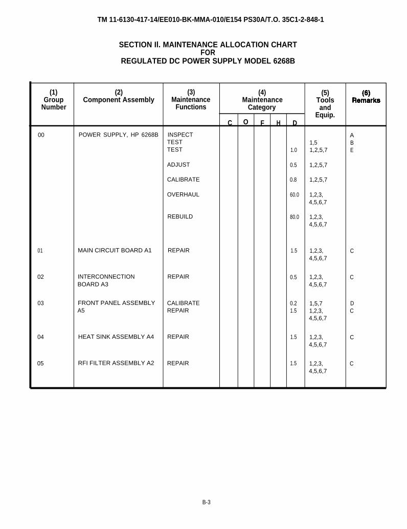
TM 11-6130-417-14/EE010-BK-MMA-010/E154 PS30A/T.O. 35C1-2-848-1
(1)Group
Number
O
00
01
02
03
04
05
SECTION Il. MAINTENANCE ALLOCATION CHARTFOR
REGULATED DC POWER SUPPLY MODEL 6268B
(2)Component Assembly
POWER SUPPLY, HP 6268B
MAIN CIRCUIT BOARD A1
INTERCONNECTIONBOARD A3
FRONT PANEL ASSEMBLYA5
HEAT SINK ASSEMBLY A4
RFI FILTER ASSEMBLY A2
(3)Maintenance
Functions
INSPECTTESTTEST
ADJUST
CALIBRATE
OVERHAUL
REBUILD
REPAIR
REPAIR
CALIBRATEREPAIR
REPAIR
REPAIR
C
(4)Maintenance
Category
F H D
1.0
0.5
0.8
60.0
80.0
1.5
0.5
0.2 1.5
1.5
1.5
(5)Toolsand
Equip.
1,51,2,5,7
1,2,5,7
1,2,5,7
1,2,3,4,5,6,7
1,2,3,4,5,6,7
1,2,3,4,5,6,7
1,2,3,4,5,6,7
1,5,71,2,3,4,5,6,7
1,2,3,4,5,6,7
1,2,3,4,5,6,7
ABE
C
C
DC
C
C
B-3
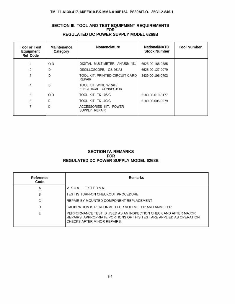
TM 11-6130-417-14/EE010-BK-MMA-010/E154 PS30A/T.O. 35C1-2-846-1
Tool or TestEquipmentRef Code
1
2
3
4
5
6
7
SECTION III. TOOL AND TEST EQUIPMENT REQUIREMENTSFOR
REGULATED DC POWER SUPPLY MODEL 6268B
MaintenanceCategory
O,D
D
D
D
O,D
D
D
Nomenclature
DIGITAL MULTIMETER, AN/USM-451
OSCILLOSCOPE, OS-261/U
TOOL KIT, PRINTED CIRCUIT CARDREPAIR
TOOL KIT, WIRE WRAP/ELECTRICAL CONNECTOR
TOOL KIT, TK-105/G
TOOL KIT, TK-100/G
ACCESSORIES KIT, POWERSUPPLY REPAIR
National/NATOStock Number
6625-00-168-0585
6625-00-127-0079
3439-00-196-0703
5180-00-610-8177
5180-00-605-0079
SECTION IV. REMARKSFOR
REGULATED DC POWER SUPPLY MODEL 6268B
ReferenceCode
A
B
C
D
E
Tool Number
Remarks
V I S U A L E X T E R N A L
TEST IS TURN-ON CHECKOUT PROCEDURE
REPAIR BY MOUNTED COMPONENT REPLACEMENT
CALIBRATION IS PERFORMED FOR VOLTMETER AND AMMETER
PERFORMANCE TEST IS USED AS AN INSPECTION CHECK AND AFTER MAJORREPAIRS. APPROPRIATE PORTIONS OF THIS TEST ARE APPLIED AS OPERATIONCHECKS AFTER MINOR REPAIRS.
B-4
TM 11-6130-417-14/EE010-BK-MMA-010/E154 PS30A/T.O. 35C1-2-848-1
APPENDIX CCOMPONENTS OF END ITEM LIST
SECTION I. INTRODUCTION
C-1. Scope. This appendix lists integral components ofand basic issue items for the HP 6268B to help you inventoryitems required for safe and efficient operation.C-2. General. This Components of End Item List is dividedinto the following sections:
a. Section Il. Integral Components of the End Item.These items, when assembled, comprise the HP 6268B and mustaccompany it whenever it is transferred or turned in. The illustra-tions will help you identify these items.
b. Section III. Basic Issue Items. These are the mini-mum essential items required to place the HP 6268B in operation,to operate it, and to perform emergency repair. Although shippedseparately packed they must accompany the HP 6268B during op-eration and whenever it is transferred between accountable offi-cers. The illustrations will assist you with hard-to-identify items.This manual is your authority to requisition replacement BII, basedon TOE/MTOE authorization of the end item.
C-3. Explanation of Columns.a. Illustration. This column is divided as follows:
(1) Figure Number. Indicates figure number of the il-lustration on which the item is shown.
(2) Item Number. The number used to identify itemcalled out in the illustration.
b. National Stock Number. Indicates the National stocknumber assigned to the item and which will be used for requisi-tioning.
c. Part Number. Indicates the primary number used bythe manufacturer, which controls the design and characteristics ofthe item by means of its engineering drawings, specifications,standards, and inspection requirements to identify an item orrange of items.
d. Description. Indicates the Federal item name and, ifrequired, a minimum description to identify the item.
e. Location. The physical location of each item Iisted isgiven in this column. The lists are designed to inventory all itemsin one area of the major item before moving on to an adjacentarea.
f. Quantity Required (Qty Reqd). This column lists thequantity of each item required for a complete major item.
g. Quantity. This column is left blank for use during aninventory. Under the Rcv’d column, list the quantity you actuallyreceive on your major item. The Date columns are for your usewhen you inventory the major item at a later date, such as forshipment to another site.
C-1
TM
11-6130-417-14
SE
CT
ION
II.
TM
11-6130-417-14/EE010-BK
-MM
A-010/E154
PS30A/T.O
. 35C
1-2-848-1
C-2
Section III.
TM 11-6130-417-14/E
E010-B
K-M
MA
-010/E154 P
S30A
/T.O. 35C
1-2-848-1
C-3
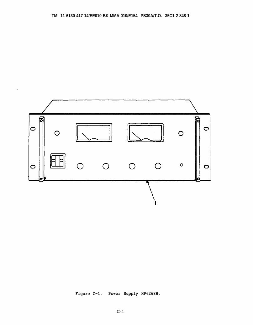
TM 11-6130-417-14/EE010-BK-MMA-010/E154 PS30A/T.O. 35C1-2-848-1
Figure C-1. Power Supply HP6268B.
C-4
TM 11-6130-417-14/EE010-BK-MMA-010/E154 PS30A/T.O. 35C1-2-848-1
APPENDIX D
ADDITIONAL AUTHORIZATION LIST
SECTION I. INTRODUCTION
D-1. Scope. This appendix lists additional items you are These items are all authorized to you by CTA, MTOE, TDA, orauthorized for the support of the HP 6268B. JTA.
D-2. General. This list identifies items that do not have to D-3. Explanation of Listing. National stock numbers,accompany the HP 6268B and that do not to be turned in with it. descriptions, and quantities are provided to help you identify and
request the additional items you require to support this equipment.
D-1
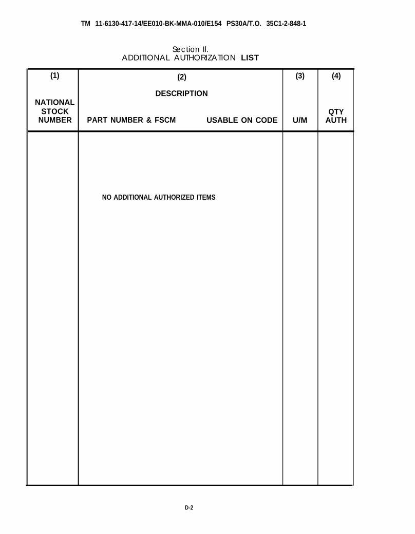
TM 11-6130-417-14/EE010-BK-MMA-010/E154 PS30A/T.O. 35C1-2-848-1
Section Il.ADDITIONAL AUTHORIZATION LIST
(1) (2) (3) (4)
DESCRIPTIONNATIONAL
STOCK QTYNUMBER PART NUMBER & FSCM USABLE ON CODE U/M AUTH
NO ADDITIONAL AUTHORIZED ITEMS
D-2
TM 11-6130-417-14/EE010-BK-MMA-010/E154 PS30A/T.O. 35C1-2-848-1
APPENDIX E
EXPENDABLE SUPPLIES AND MATERIALS LIST
SECTION I. INTRODUCTION
E-1. Scope. This appendix lists expendable supplies andmaterials you will need to operate and maintain the HP 6268B.These items are authorized to you by CTA 50-970, ExpendableItems (Except Medical, Class V, Repair Parts, and Heraldic Items).
E-2. Explanation of Columns.a. Column 1 - Item Number. This number is assigned
to the entry in the Iisting and is referenced in the narrative instruc-tions to identify the material (e.g., “Use cleaning compound, item
5, App. D”).b. Column 2 - Level. This column identifies the lowest
level of maintenance that requires the listed item.C - Operator/CrewO - Organizational MaintenanceF - Direct Support MaintenanceH - General Support Maintenance
c. Column 3 - National Stock Number. This is the Na-tional stock number assigned to the item; use it to request or re-quisition the item.
d. Column 4 - Description. Indicates the Federal itemname and, if required, a description to identify the item. The lastline for each item indicates the part number followed by the Fed-eral Supply Code for Manufacturer (FSCM) in parentheses, if ap-plicable.
e. Column 5 - Unit of Measure (U/M). Indicates themeasure used in performing the actual maintenance function. Thismeasure is expressed by a two-character alphabetical abbreviation(e.g., ea, in, pr). If the unit of measure differs from the unit of is-sue, requisition the lowest unit of issue that will satisfy your re-quirements.
E-1
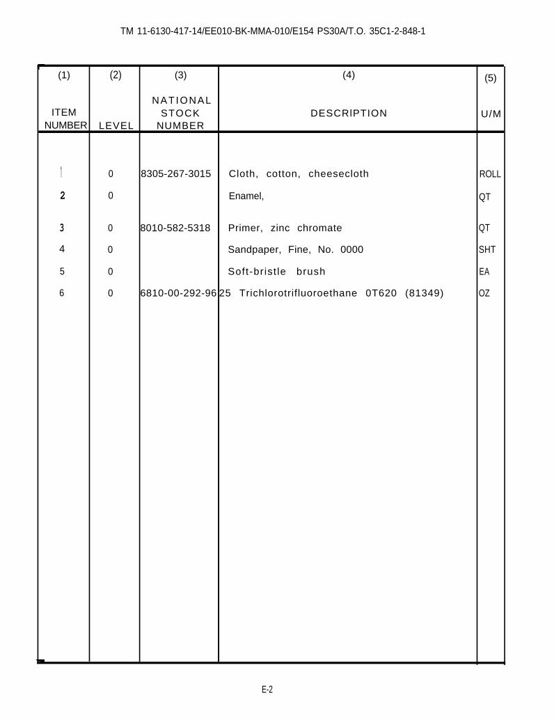
TM 11-6130-417-14/EE010-BK-MMA-010/E154 PS30A/T.O. 35C1-2-848-1
(1) (2) (3) (4) (5)
NATIONALITEM STOCK DESCRlPTION U/M
NUMBER LEVEL NUMBER
1 0 8305-267-3015 Cloth, cotton, cheesecloth ROLL
2 0 Enamel, QT
3 0 8010-582-5318 Primer, zinc chromate QT
4 0 Sandpaper, Fine, No. 0000 SHT
5 0 Soft-br ist le brush EA
6 0 6810-00-292-96 25 Trichlorotrifluoroethane 0T620 (81349) OZ
E-2
TM 11-6130-417-14/EE010-BK-MMA-010/E154 PS30A/T.O. 35C1-2-848-1
ALPHABETICAL INDEX
Subject
Accessory Equipment Available
Adjustment and Calibration,
Ammeter
A
Constant-Current Programming
Constant-Voltage Programming
Crowbar Trip Voltage
Disabling the Crowbar
Load Transient Recovery Time
Maximum Crowbar Trip Voltage
Meter Zero
Overvoltage Trip Point
Preregulator Tracking
Ripple Balance
Additional Protection Features
Ammeter Accuracy
Amplifiers,
Error
Mixer
Auto-Parallel,
Operation
Overvoltage Protection
Remote Programming
Remote Sensing
Setting the Voltage and Current Controls
Auto-Series,
Determining the Value for Rx
Operation
Overvoltage Protection
Remote Programming
Remote Sensing
Setting the Current Controls
Setting the Voltage Controls
Auto-Tracking,
Determining the Value for Rx
Operation
Overvoltage Protection
Remote Programming
Remote Sensing
Setting the Voltage and Current Controls
B
Battery,
Charging
Constant Current Discharge
Discharging
Taper Charge
Paragraph
C
1-19
5-71
5-89
5-79
5-104
5-108
5-98
5-106
5-73
3-12
5-102
5-100
4-70
5-41
4-51
4-49
3-51
5-54
3-56
3-55
3-53
3-60
3-57
3-64
3-66
3-65
3-63
3-62
3-69
3-67
3-72
3-75
3-74
3-71
3-87
3-94
3-91
3-90
Capacitance, Output
Charging, Battery
Check,
Electrical
Mechanical
Circuit,
Detailed Circuit Analysis
Meter
Overvoltage Limit
Preregulator Control Circuit
Short Circuit Protection
Turn-On Control
Voltage Clamp
Comparator,
Constant Current
Constant Voltage
Connecting the Load
Constant Current,
Comparator
Operation
Output, Resistance Input
Output, Voltage Input (fixed gain)
Output, Voltage Input (variable gain),
Programming Calibration
Tests
Constant Voltage,
Comparator
Operation
Output, Resistance Input
Outputj Voltage Input (unit gain)
Output, Voltage Input (variable gain)
Programming Calibration
Tests
Control Circuit, Preregulator
Controls, Setting the Voltage and Current
Auto Series
Auto-Tracking
Auto-Parallel
Crowbar,
Disabling the
Overvoltage Protection
Trip Voltage Adjustment
Current,
Output
Reverse Loading
Conversion, Input Line Voltage or Frequency
3-79
3-87
2-5
2-3
5-16
4-66
4-27
4-17
4-31
4-58
4-45
4-40
4-33
3-15
4-40
3-10
5-45
3-47
3-48
5-89
5-38
4-33
5-3
3-39
3-41
3-42
5-79
5-7
4-17
3-62, 63
3-71
3-53
5-108
4-52
5-104
5-41
3-85
2-17
Index-1
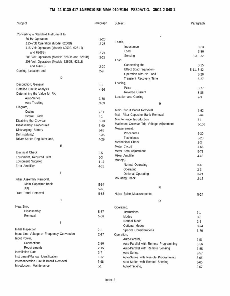
TM 11-6130-417-14/EE010-BK-MMA-010/E154 PS30A/T.O. 35C1-2-848-1
Subject Paragraph
Converting a Standard Instrument to,50 Hz Operation 2-28115-Volt Operation (Model 6260B) 2-26115-Volt Operation (Models 6259B, 6261 B
and 6268B) 2-24208-Volt Operation (Models 6260B and 6269B) 2-22208-Volt Operation (Models 6259B, 6261B
and 6268B)Cooling, Location and
Description, GeneralDetailed Circuit AnalysisDetermining the Value for Rx,
Auto-SeriesAuto-Tracking
Diagram,OutlineOverall Block
Disabling the CrowbarDisassembly ProceduresDischarging, BatteryDrift (stability)Driver Series Regulator and,
Electrical CheckEquipment, Required TestEquipment SuppliedError Amplifier
Filter Assembly Removal,Main Capacitor BankRFI
Front Panel Removal
Heat Sink,DisassemblyRemoval
Initial Inspection
2-202-9
D
1-14-16
3-603-69
2-114-15-1085-603-915-354-29
E
2-55-31-174-51
F
5-645-655-63
H
5-675-66
I
2-1Input Line Voltage or Frequency Conversion 2-17Input Power,
Connections 2-30Requirements 2-15
Installation Data 2-7Instrument/Manual Identification 1-12Interconnection Circuit Board Removal 5-68Introduction, Maintenance 5-1
Subject
L
Leads,InductanceLoadSensing
Load,Connecting theEffect (load regulation)Operation with No LoadTransient Recovery Time
Loading,PulseReverse Current
Location and Cooling
M
Main Circuit Board RemovalMain Filter Capacitor Bank RemovalMaintenance IntroductionMaximum Crowbar Trip Voltage AdjustmentMeasurement,
ProceduresTechniques
Mechanical CheckMeter CircuitMeter Zero AdjustmentMixer AmplifierMode(s),
Normal OperatingOperatingOptional Operating
Mounting, Rack
Noise Spike Measurements
Operating,InstructionsModesNormal ModeOptional ModesSpecial Considerations
Operation,Auto-Parallel,
Paragraph
3-333-30
3-31, 32
3-155-11, 5-42
3-205-27
3-773-852-9
5-625-645-15-106
5-305-282-34-665-734-48
3-63-33-242-13
5-24
N
O
3-13-33-63-243-76
3-51Auto-Parallel with Remote Programming 3-56Auto-Parallel with Remote Sensing 3-55Auto-Series, 3-57Auto-Series with Remote Programming 3-66Auto-Series with Remote Sensing 3-65Auto-Tracking, 3-67
Index-2
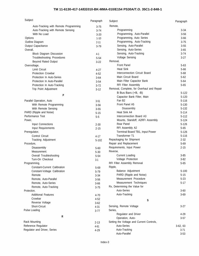
TM 11-6130-417-14/EE010-BK-MMA-010/E154 PS30A/T.O. 35C1-2-848-1
Subject
Auto-Tracking with Remote ProgrammingAuto-Tracking with Remote SensingWith No Load
OptionsOutline DiagramOutput CapacitanceOverall,
Block Diagram DiscussionTroubleshooting ProceduresBeyond Rated Output
Overvoltage,Limit CircuitProtection CrowbarProtection In Auto-SeriesProtection In Auto-ParallelProtection In Auto-TrackingTrip Point Adjustment
P
Parallel Operation, AutoWith Remote ProgrammingWith Remote Sensing
PARD (Ripple and Noise)Performance TestPower,
Input ConnectionsInput Requirements
Preregulator,Control CircuitTracking Adjustment
Procedure,DisassemblyMeasurement:Overall TroubleshootingTurn-On Checkout
Programming,Constant-Current CalibrationConstant-Voltage CalibrationRemoteRemote, Auto-ParallelRemote, Auto-SeriesRemote, Auto-Tracking
Protection,Additional FeaturesCrowbarReverse VoltageShort-Circuit
Pulse Loading
Rack MountingReference RegulatorRegulator and Driver, Series
Paragraph
3-753-743-201-102-113-79
4-15-543-22
4-274-523-643-543-723-12
3-513-563-555-155-5
2-302-15
4-175-102
5-605-305-543-1
5-695-793-343-563-663-75
4-704-523-624-313-77
R
2-134-614-29
Subject
Remote,ProgrammingProgramming, Auto-ParallelProgramming, Auto SeriesProgramming, Auto-TrackingSensing, Auto-ParallelSensing, Auto-SeriesSensing, Auto-TrackingVoltage Sensing
Removal,Front PanelHeat SinkInterconnection Circuit BoardMain Circuit BoardMain Filter Capacitor BankRFI Filter Assembly
Removal, Complete, for Overhaul and RepairB Bus Bars (+B, -B)Capacitor Bank Filter, MainFan B2Front Panel A5
DisassemblyHeat Sink A4Interconnection Board A3Mounts, Standoff, A2RFI AssemblyRear PanelRFI Assembly A2Terminal Board TB1, Input PowerTransformer T1
Repackaging for ShipmentRepair and ReplacementRequirements, Input PowerReverse,
Current LoadingVoltage Protection
RFI Filter Assembly RemovalRipple,
Balance AdjustmentPARD (Ripple and Noise)Measurement ProcedureMeasurement Techniques
Rx, Determining the Value forAuto-SeriesAuto-Tracking
S
Sensing, Remote VoltageSeries,
Regulator and DriverOperation, Auto-
Setting the Voltage and Current Controls,Auto-SeriesAuto-TrackingAuto-Parallel
Index-3
Paragraph
3-343-563-663-753-553-653-743-27
5-635-665-685-625-645-65
5-1225-1205-1165-1305-1325-1145-1125-1245-1265-655-1265-1162-325-692-15
3-853-825-65
5-1005-155-235-17
3-603-69
3-27
4-293-57
3-62, 633-713-53
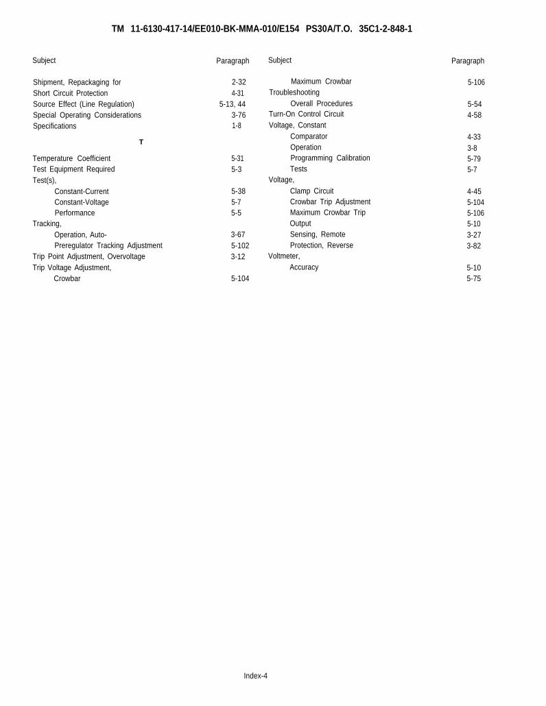
Subject
TM 11-6130-417-14/EE010-BK-MMA-010/E154 PS30A/T.O. 35C1-2-848-1
Shipment, Repackaging forShort Circuit ProtectionSource Effect (Line Regulation)Special Operating ConsiderationsSpecifications
T
Temperature CoefficientTest Equipment RequiredTest(s),
Constant-CurrentConstant-VoltagePerformance
Tracking,Operation, Auto-Preregulator Tracking Adjustment
Trip Point Adjustment, OvervoltageTrip Voltage Adjustment,
Crowbar
Paragraph
2-324-31
5-13, 443-761-8
5-315-3
5-385-75-5
3-675-1023-12
5-104
Subject
Maximum CrowbarTroubleshooting
Overall ProceduresTurn-On Control CircuitVoltage, Constant
ComparatorOperationProgramming CalibrationTests
Voltage,Clamp CircuitCrowbar Trip AdjustmentMaximum Crowbar TripOutputSensing, RemoteProtection, Reverse
Voltmeter,Accuracy
Paragraph
5-106
5-544-58
4-333-85-795-7
4-455-1045-1065-103-273-82
5-105-75
Index-4
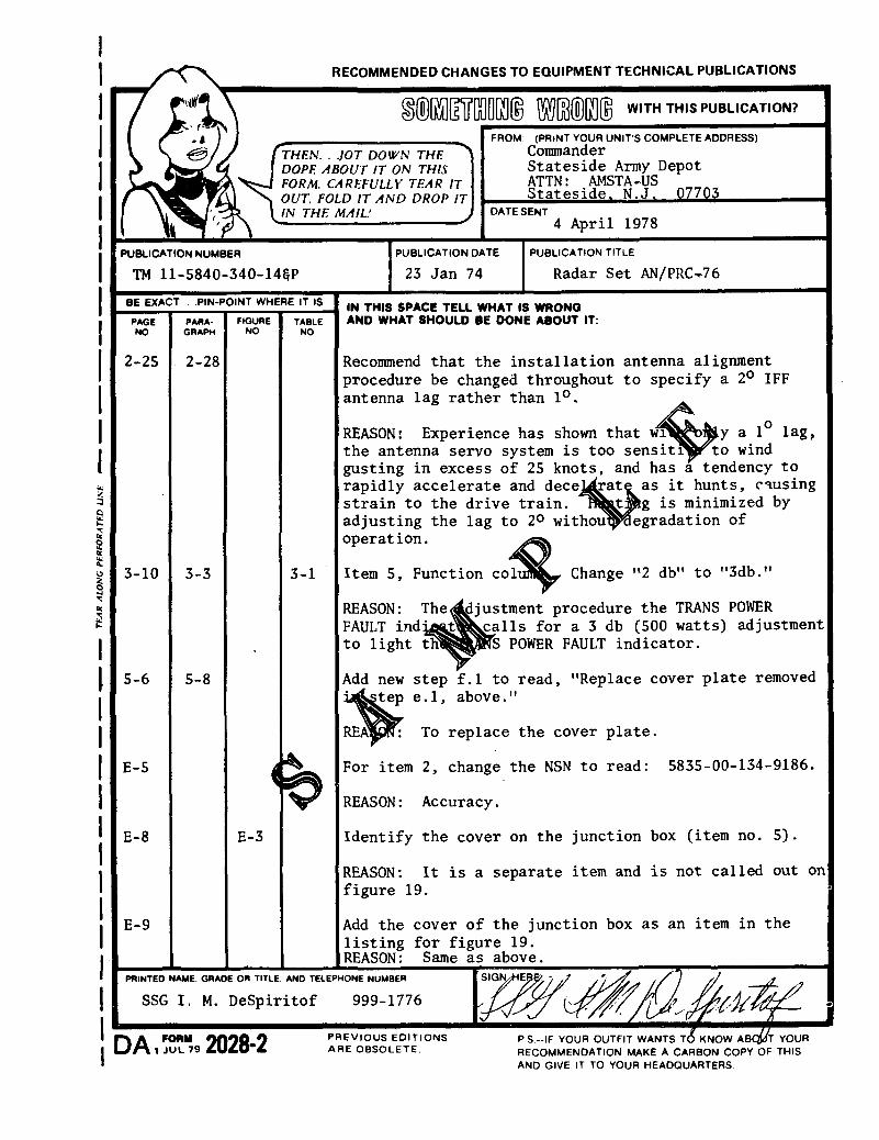

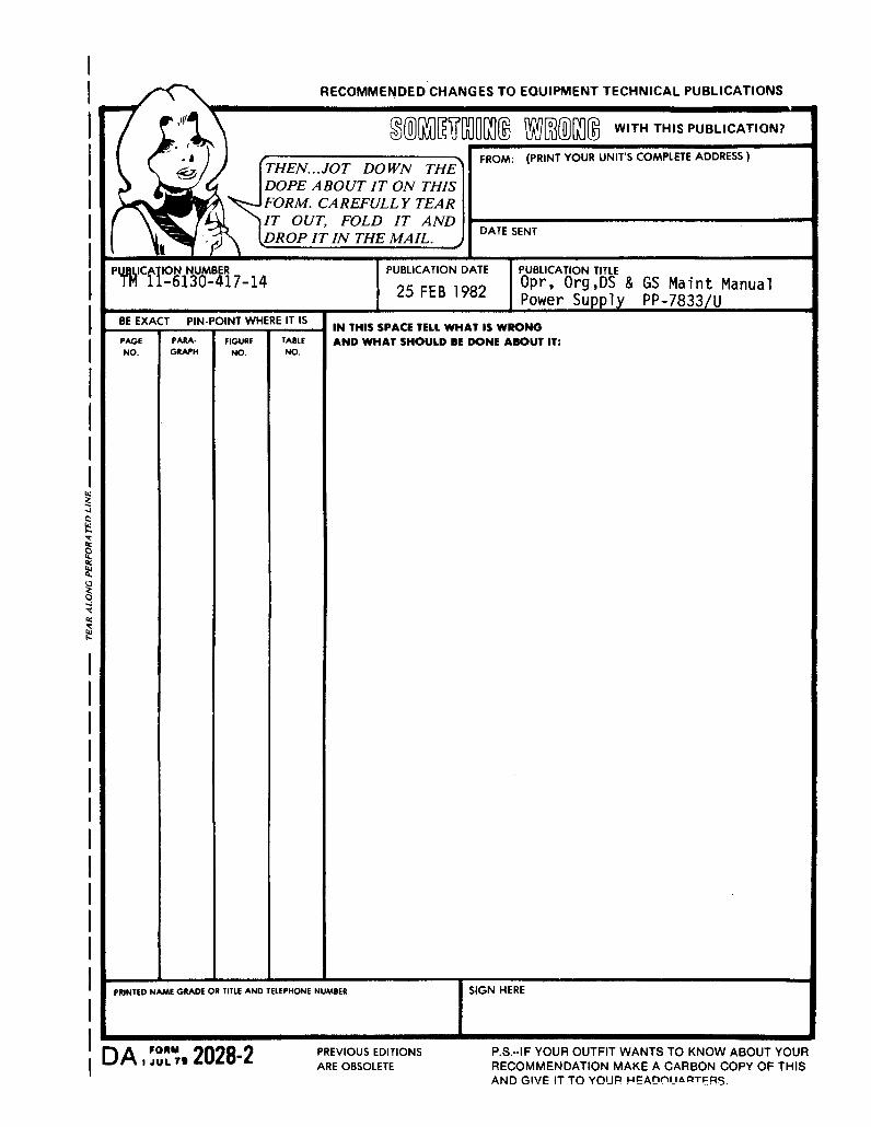
By Order of the Secretaries of the Army, the Navy, and the Air Force
Official:ROBERT M. JOYCE
Major General United States ArmyThe Adjutant General
Official:JAMES P. MULLINS
General, USAF, Commander, Air ForceLogistics Command
DISTRIBUTION:
To be distributed in accordance with Special List.
E. C. MEYERGeneral, United States Army
Chief of Staff
G. B. SHICKRear Admiral United States Navy
Commander, Naval ElectronicSystems Command
CHARLES A. GABRIEL, General USAFChief of Staff
* U.S. GOVERNMENT PRINTING OFFICE : 1989 0 - 242-451 (1553)

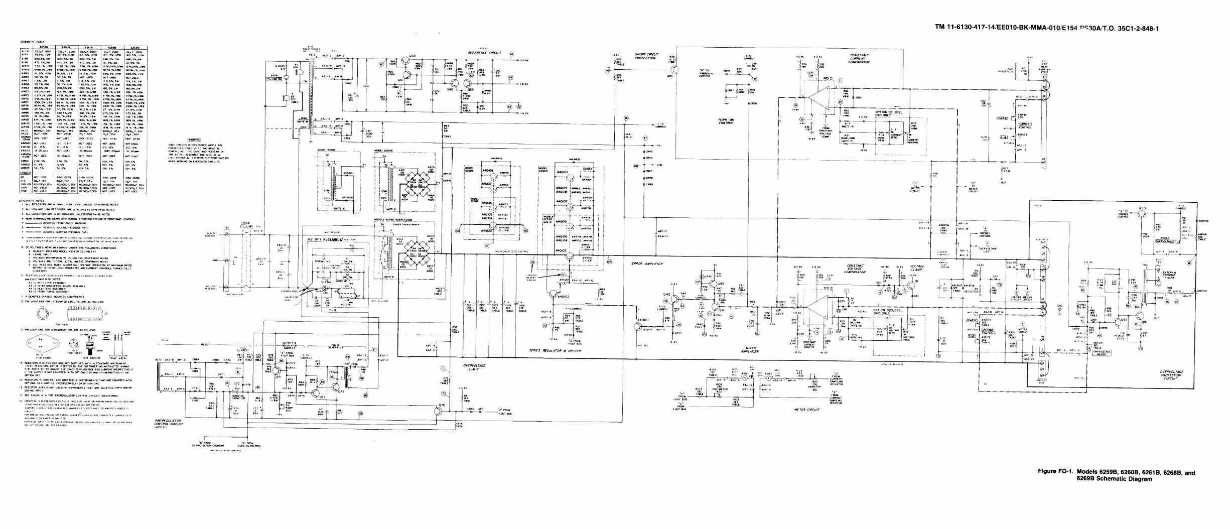
TM11-6130-417-14
Figure FO-1
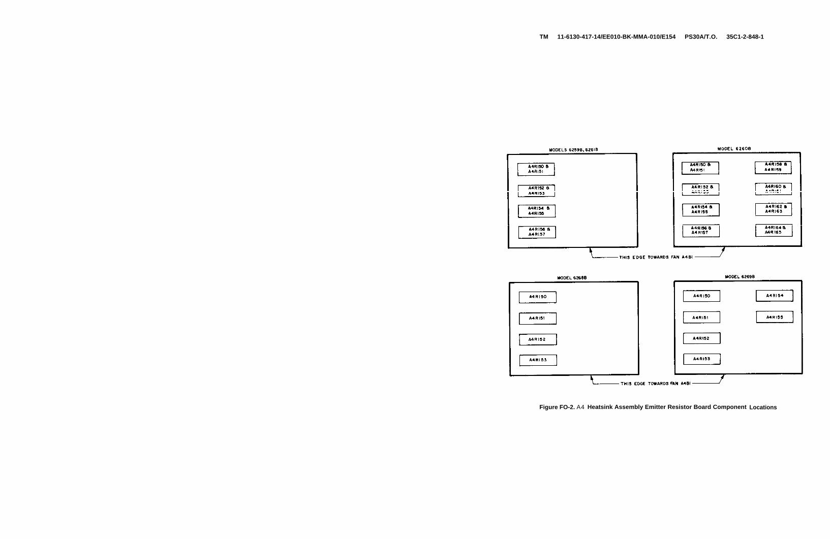
TM 11-6130-417-14/EE010-BK-MMA-010/E154 PS30A/T.O. 35C1-2-848-1
Figure FO-2. A4 Heatsink Assembly Emitter Resistor Board Component Locations
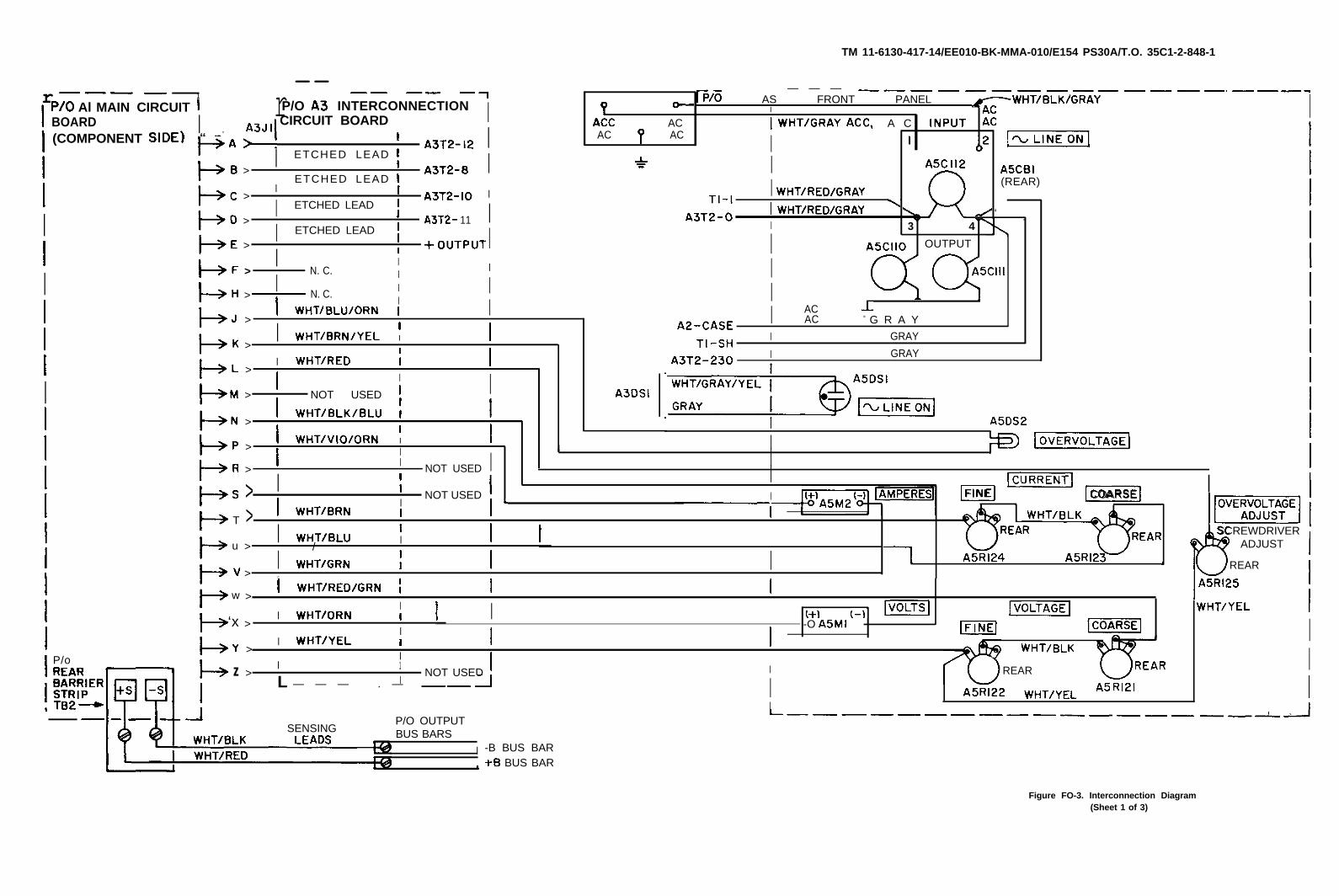
TM 11-6130-417-14/EE010-BK-MMA-010/E154 PS30A/T.O. 35C1-2-848-1
r .—— — 1
IIII
II
I
I
III
I
II
IIIII
I
P1O Al MAIN CIRCUIT IBOARD(COMPONENT
ISIDE) “ p’ ~
P
P/o
l-+
1+
T
u
v
w
‘x
l-+ Y
i-+ z
I..
+
A3DSI
r—— —— —— —P/O A3 INTERCONNECTION 1,
i_P/O AS FRONT PANEL ~— — — —— —— —. —— —— —— ——
I ? * WHT/BLK/GRAY
*3J, CIRCUIT BOARDI
>1 IACC AC I WHT/GRAY ACC, A C lNpuT ::
I AC Y AC
>I
A3T2-12 I I # ~ETCHED LEAD I
I
>I
A3T2-8 I I A5CI12ETCHED LEAD I
A5CBI
f I I (REAR)
\
>I
A3T2-10 WHT/RED/GRAYETCHED LEAD T1-1
i /‘ .
>I
I I WHT/RED/GRAYA3T2- 11 A3T2-O
ETCHED LEAD I: I
3 4
>I I +OUTPUT
I
I A5CII0 OUTPUT
I
>I
N. C. II
IN. C. I
1>
II I
IWHT/BLU/ORN 1 I AC
>I I I *2-CASE
AC = G R A Y
WHT/BRN/YEL ITI-SH
I
>I
GRAYI
II GRAY
WHT/RED i A3T2-230
>I
I
NOT USED 1 IWHT/BLK/BLU :
>I :Zzn@lii,
>I
II
I A5DS2
WHT/VIO/ORN I4
>I
I [OVERVOLTAGE]II NOT USED I I
> I I I I1 ~1 ImEml ,—1 I> I
NOT USED I FINE COARSEI
WHT/BRN 1-1 I
>I I
WHT/BLU I II/
>I I
WHT/GRN I I I A5R124 im .
.— —.
/!!7mmSCREWDRIVER
ADJUST
REAR
1+—.—SENSING
P/O OUTPUTBUS BARS
I
L.— —— —— —— —— ,— _ __ _
-B BUS BAR+B BUS BAR
A5R125I WHT/RED/GRN :>
I I
>I
IWHT/ORN I II (+) (-,’ m IEmEl WHT/
>I
II I
-O A5MIm mm
WHT/YEL I
>I
WHT/BLKI1
NOT USED I IL -1
REARI— — — . — —— I A5R122 WHT/YEL
A5R121
I
‘YEL
II
I
II
III
I
II
III
IIII
Figure FO-3. Interconnection Diagram(Sheet 1 of 3)
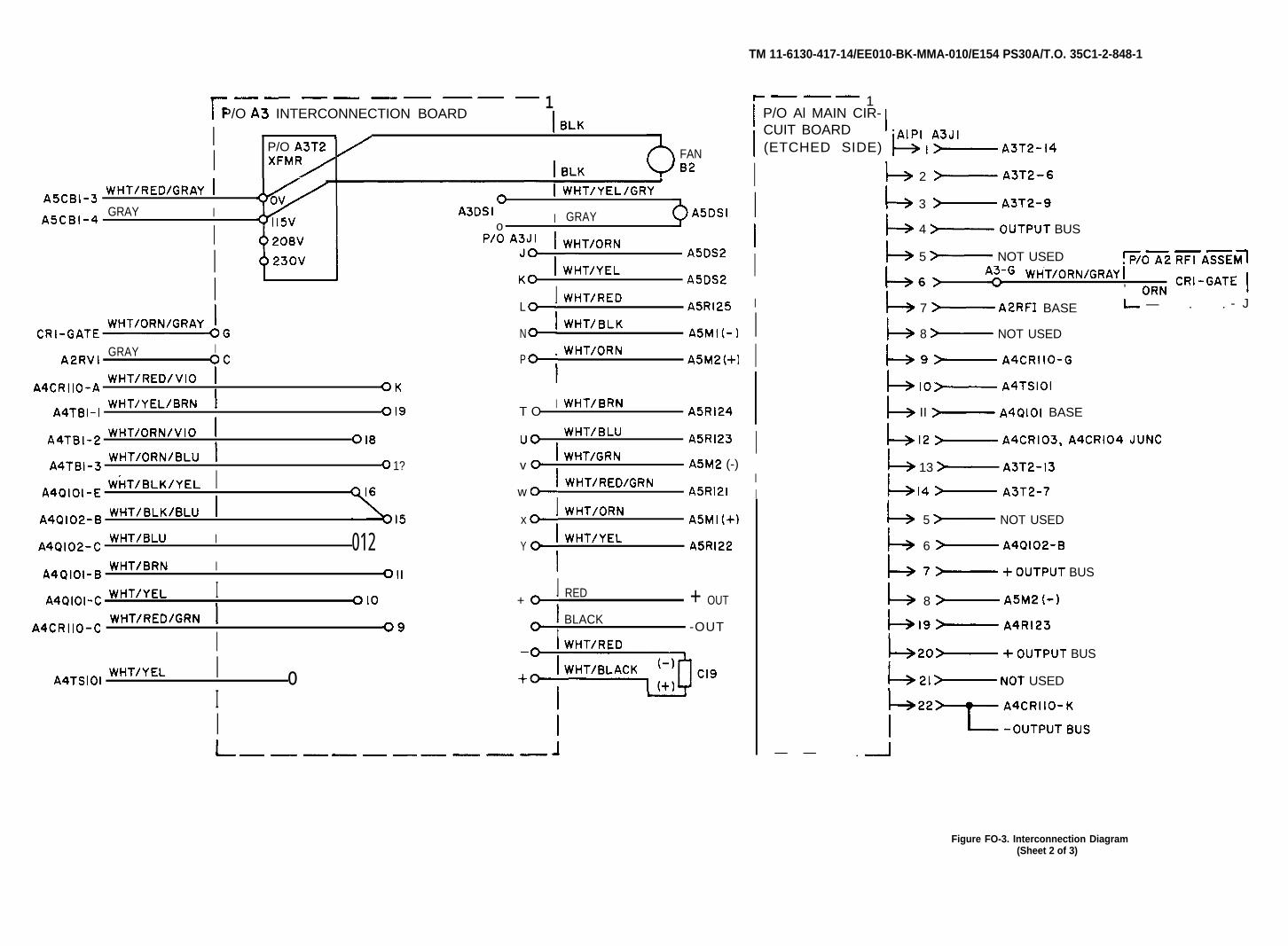
TM 11-6130-417-14/EE010-BK-MMA-010/E154 PS30A/T.O. 35C1-2-848-1
r .— —— —— —— .P/O A3 INTERCONNECTION BOARD
1
I I BLK*
IP/O A3T2XFMR FAN
! BLK r32
A5CBI-3WHT/RED/GRAY I
IA5CBI-4
GRAY
III
WHT/ORN/GRAY ICR1-GATE~G
GRAY IA2RVI Oc
A4CRII0-AWHT/RED/VIO ]
IQK
A4TBI-IWHT/YEL/BRN
019
A4TBI-2WHT/ORN/VIO
I018
A4TBI-3WHT/ORN/BLU
IQ 1?
A4QIOI-EWHT/BLK/YEL
IA4QI02-BWHT/BLK/BLU
I
15
A4QI02-CWHT/BLU
I
012A4QIOI-B
WHT/BRN
I011
A4QIOI-C WHT/YEL
I
010
A4CRII0-CWHT/RED/GRN
I09
WHT/YEL IA4TSIOI
Io
I
o ! WHT/YEL/GRY
A3DS Io
I GRAY A5DSI
A5DS2
KO A5DS2
L I WHT/REDA5R125
:1 WHT/BLKN A5MI(-)
WHT/ORNP
‘1
A5M2(+)
T OI WHT/BRN
A5R124
UoWHT/BLU A5R123
vI WHT/GRN
A5M2 (-)
:1 WHT/RED/GRNw
IA5R121
xWHT/ORN
;1A5MI(+)
YWHT/YEL
A5R122
I
+I RED
:1+ OUT
BLACKI -OUT
1-. — —. . —— — — — 1
r —— .
I1
P/O Al MAIN CIR-CUIT BOARD I
(ETCHED SIDE) ~ I &- A3T2-14
I l-+ 2 ~ A3T2-6
I I-9 3 ~ A3T2-9
1+ 4 ~OUTPUT BUS
I 1+ 5 ~ NOT USED ~o~2KA=~
1-+>A3-G wHT/oRN/GRAyl
I
6 , ORN CRI-GATE I
Il-+ 7 ~ A2RFI BASE L — . . - J
b 8 ~ NOT USED
I l-+ 9~A4cRllo-G
l-+ lo~ A4TSIOI
L II >—A4QIOI BASE
I l-+ 12>—A4CRI03, A4CRI04 JUNC
IL 13 ~ A3T2-13
I L 14 ~ A3T2-7
LL1+1+
5 ~ NOT USED
6 ~ A4QI02-B
7~+OUTPUT BUS
8 ~A5M2 (-)
1+ 19~A4R123
l--+20~+OUTPUT BUS
L 21 ~ NOT USED
p22Tn:;;;:us
— — . J
Figure FO-3. Interconnection Diagram(Sheet 2 of 3)
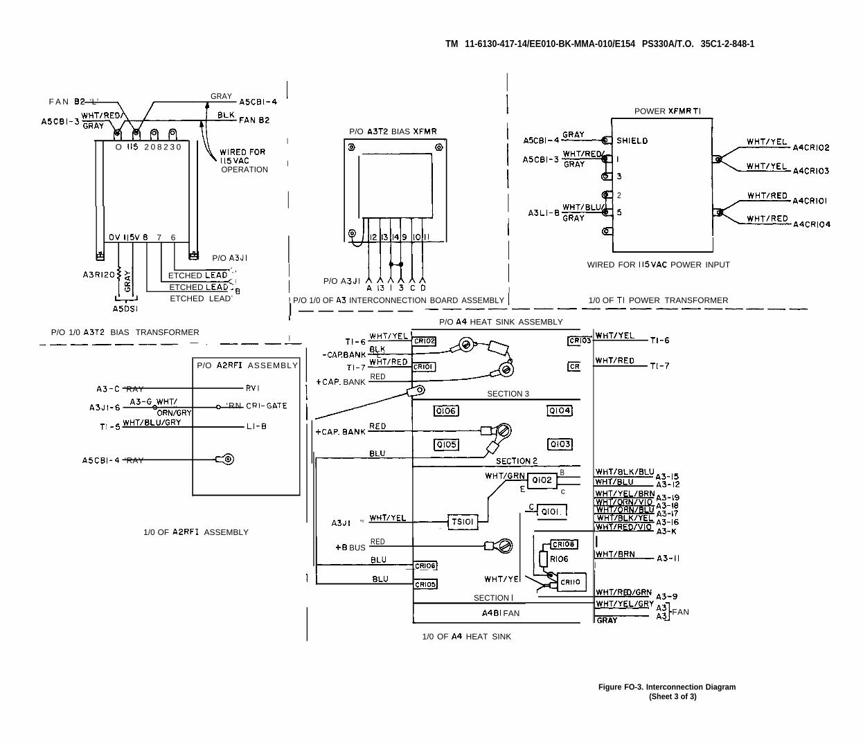
TM 11-6130-417-14/EE010-BK-MMA-010/E154 PS330A/T.O. 35C1-2-848-1
F A N B2 ‘L’GRAY
A5CBI-4I
O 1!5 2 0 8 2 3 0I
OPERATIONI
OV I15V8 7 6
&
A3R120 ETCHED LEAD’”} :ETCHED LEAD< ~ETCHED LEAD<
I
P/O A3JI
P/O A3T2 BIAS XFMR.
II POWER XFMR TI
I [ I
I! P/O A
A1313CD I
I 4 2
WHT/BLU/ ~
IA3LI-B GRAY
I d k=WHT/RED A4CR,01
WHT/RED A4CR104
! P/O 1/0 OF A3 INTERCONNECTION BOARD ASSEMBLY t
I L IWIRED FOR I15VAC POWER INPUT
1/0 OF TI POWER TRANSFORMERA5DSI l — — — — — — -–———’—————————————
I
P/O 1/0 A3T2 BIAS TRANSFORMERI
-—— —— —— — . —— ——
P/O A2RFI ASSEMBLY
A3-C ‘RAY RV I
A3JI-6A3-GAwHT/
‘ORN/GRY: ‘RN cRI-GATE
T, -5 WHT/BLU/GRY L1-0
A5CBI-4 ‘RAY
1/0 OF A2RFI ASSEMBLY
II
P/O A4 HEAT SINK ASSEMBLY
TI-6
=
WHT/YEL ~Rlo
-CAP.BANK ‘ L ’T,_7 WHT/RED
CRIOI
+CAP. BANKRED
SECTION 3
m ml
+CAP. BANK~~@
mBLU
B
c
A3J, ,0 WHT/YELWRrl
RED+B BUS =@
BLU—CRI06]
1] BLUcRI05
WHT/YE
SECTION IECRI08
RI06
CRIIO
1 A4BI FAN
1/0 OF A4 HEAT SINK
WHT/YELTI-6
WHT/REDTI-7
lWHT/BLK/BLUA3-,5WHT/BLU A3-12.
A3-19m;
A3-16A3-K
I~A3-11I
k=WHT/R D/GRN A3_9WHT/YEL/GRY s
113 FAN
GRAY
Figure FO-3. Interconnection Diagram(Sheet 3 of 3)


PIN : 052771-000

This fine document...
Was brought to you by me:
Liberated Manuals -- free army and government manuals
Why do I do it? I am tired of sleazy CD-ROM sellers, who take publicly available information, slap “watermarks” and other junk on it, and sell it. Those masters of search engine manipulation make sure that their sites that sell free information, come up first in search engines. They did not create it... They did not even scan it... Why should they get your money? Why are not letting you give those free manuals to your friends?
I am setting this document FREE. This document was made by the US Government and is NOT protected by Copyright. Feel free to share, republish, sell and so on.
I am not asking you for donations, fees or handouts. If you can, please provide a link to liberatedmanuals.com, so that free manuals come up first in search engines:
<A HREF=http://www.liberatedmanuals.com/>Free Military and Government Manuals</A>
– SincerelyIgor Chudovhttp://igor.chudov.com/
– Chicago Machinery Movers