Embed Size (px)
Citation preview

From Technologies to Market
Power Electronics Overview:
What are the markets and
trends?
From Technologies to Market
© 2015© 2015
3
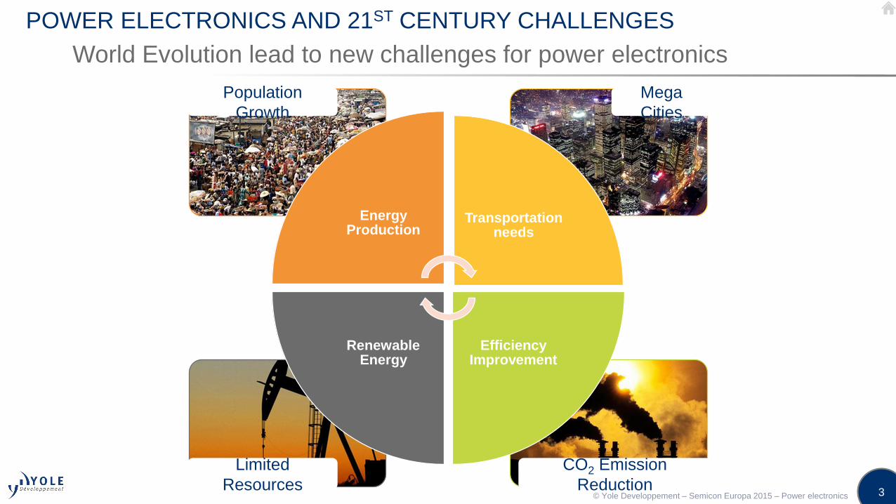
POWER ELECTRONICS AND 21ST CENTURY CHALLENGES
World Evolution lead to new challenges for power electronics
Energy Production
Transportationneeds
Efficiency Improvement
RenewableEnergy
Population
Growth
Mega
Cities
Limited
Resources
CO2 Emission
Reduction© Yole Developpement – Semicon Europa 2015 – Power electronics

4
POWER ELECTRONICS AND 21ST CENTURY CHALLENGES
Power device market evolution between 2006 and 2020
2014 growth was smaller than expected but still high. Forecasts for 2020 for power modules show a regular growth
+8.4%
© Yole Developpement – Semicon Europa 2015 – Power electronics

5
Low Voltage400 -> 900V
Medium Voltage1.2kV -> 1.7kV
High Voltage2kV -> 3.3 kV
Very High Voltage> 3.3kV
2014 $8,430M $2,036M $748M $327M
2020 $11,881M $3,541M $1,208M $552M
$M
$2,000M
$4,000M
$6,000M
$8,000M
$10,000M
$12,000M
$14,000MPower Electronics, by voltage. Comparison 2014 - 2020
POWER ELECTRONICS AND 21ST CENTURY CHALLENGES
What evolution for power devices between 2014 and 2020? Split per voltage
Medium voltage devices will have the highest growth by 2020, whereas very high voltage devices market will know very little growth
+41%
+74%
+61%+69%
Very high voltage
devices growth is driven
by energy T&D, while
energy production uses
mainly medium (or low)
voltage devices
© Yole Developpement – Semicon Europa 2015 – Power electronics

6
POWER ELECTRONICS AND 21ST CENTURY CHALLENGES
What evolution for power devices between 2014 and 2020? Split per type of device
Even though each product type market will grow, the biggest increase will be in power modules
Modules will
increase
considerably,
while
MOSFETs will
suffer from
the smallest
growth
© Yole Developpement – Semicon Europa 2015 – Power electronics
7
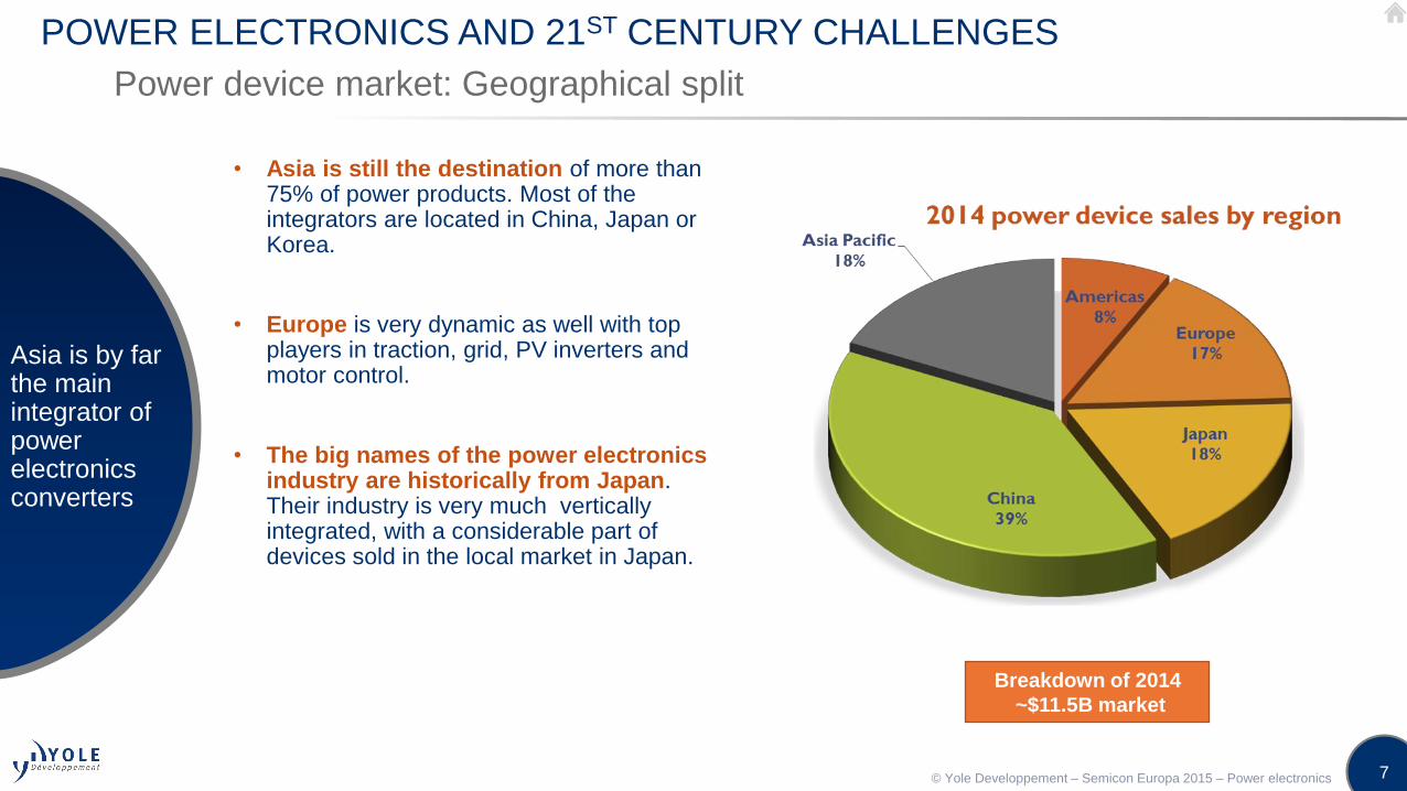
POWER ELECTRONICS AND 21ST CENTURY CHALLENGES
Power device market: Geographical split
• Asia is still the destination of more than 75% of power products. Most of the integrators are located in China, Japan or Korea.
• Europe is very dynamic as well with top players in traction, grid, PV inverters and motor control.
• The big names of the power electronics industry are historically from Japan. Their industry is very much vertically integrated, with a considerable part of devices sold in the local market in Japan.
Asia is by far the main integrator of power electronics converters
Breakdown of 2014
~$11.5B market
© Yole Developpement – Semicon Europa 2015 – Power electronics
8
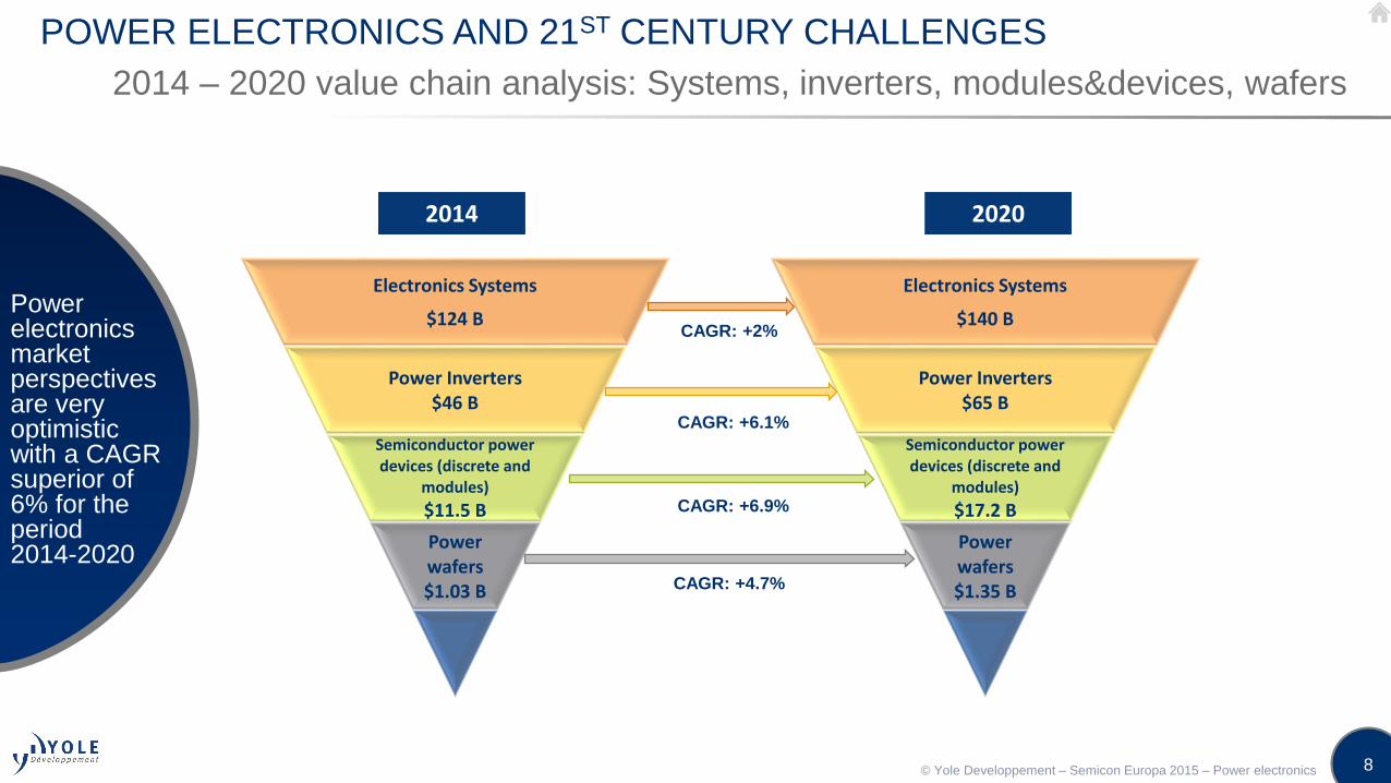
POWER ELECTRONICS AND 21ST CENTURY CHALLENGES
2014 – 2020 value chain analysis: Systems, inverters, modules&devices, wafers
Power electronics market perspectives are very optimistic with a CAGR superior of 6% for the period 2014-2020
Electronics Systems
$124 B
Power Inverters$46 B
Semiconductor power devices (discrete and
modules)
$11.5 B
Power wafers$1.03 B
Electronics Systems
$140 B
Power Inverters$65 B
Semiconductor power devices (discrete and
modules)
$17.2 B
Power wafers$1.35 B
2014 2020
CAGR: +4.7%
CAGR: +6.9%
CAGR: +2%
CAGR: +6.1%
© Yole Developpement – Semicon Europa 2015 – Power electronics

9
POWER ELECTRONICS AND 21ST CENTURY CHALLENGES
Power electronics market split per application and main expectations by 2020 (in M$)
Automotive and industry market shares are expected to grow by 2020
Breakdown of 2014
~$11.5B marketBreakdown of 2020
~$17.2B market
© Yole Developpement – Semicon Europa 2015 – Power electronics
11
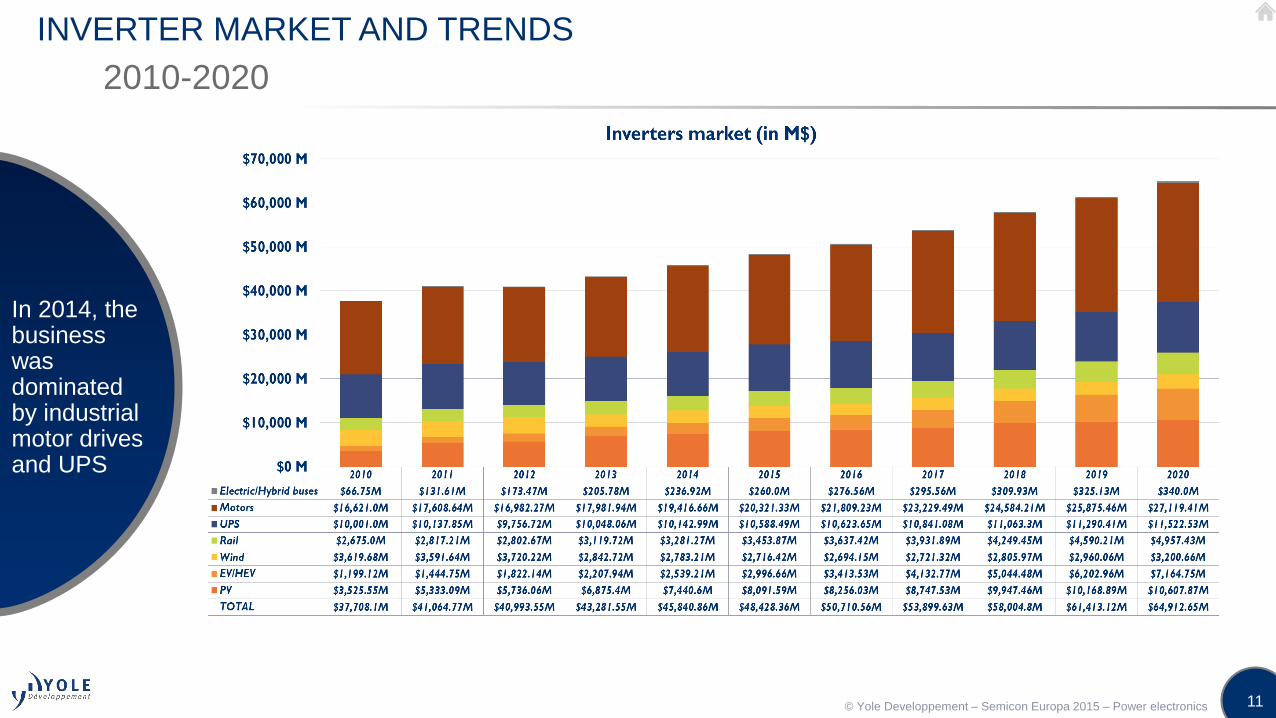
INVERTER MARKET AND TRENDS
2010-2020
In 2014, the business was dominated by industrial motor drives and UPS
© Yole Developpement – Semicon Europa 2015 – Power electronics

12
INVERTER MARKET AND TRENDS
Overall inverter market in 2014 exceeded $45 billion
Andothers…
Drivers for inverter innovation
Drivers for application growth
Size reduction
Weight reduction
Efficiency improvement
Cost reduction
• Increase of CO2 emission taxes
• Demand and regulations for clean energy generation
• Need for mass transportation
• Need for efficient transportation
• Regulation on energy efficiency
• Data center and data storage market increase
• Utility grid stress increasing due to the use of clean energy
Depending on applications
Wind turbines$2.7 B -2.1%
PV inverter$7 B +2.2%
Motor drives
$19.4 B +8%
Rail traction$3.3 B +5.2%
UPS$10 B +0.9%
EV/HEV$2.5 B +15%
Inverter markets*
* In 2014
© Yole Developpement – Semicon Europa 2015 – Power electronics
13
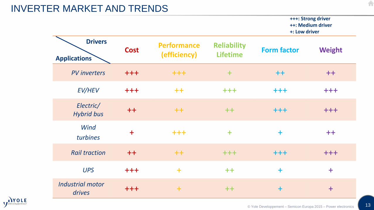
INVERTER MARKET AND TRENDS
Drivers
ApplicationsCost
Performance(efficiency)
ReliabilityLifetime
Form factor Weight
PV inverters +++ +++ + ++ ++
EV/HEV +++ ++ +++ +++ +++
Electric/ Hybrid bus ++ ++ ++ +++ +++
Wind
turbines+ +++ + + ++
Rail traction ++ ++ +++ +++ +++
UPS +++ + ++ + +
Industrial motor drives +++ + ++ + +
+++: Strong driver++: Medium driver+: Low driver
© Yole Developpement – Semicon Europa 2015 – Power electronics

14
INVERTER MARKET AND TRENDS
Technical breakthrough required in power electronics
$/kW
kW/kg
kW/l
Power Assembly Architecture
Technical
Breakthrough
Passive Elements (Cooling, capacitors, busbars, etc…)
Power Packaging
Wide Band gap Semiconductors
• Converter Topologies (mainly for LV-HV DC/DC and AC/DC)
• Inverter has to be developed according to the electric motor
• High Temperature Capacitors, Laminated Busbars
• Enhanced cooling of the power converter
• High Temperature operation
• More compact inverters
• Low stray inductance packaging
• High Temperature and reliable assemblies
© Yole Developpement – Semicon Europa 2015 – Power electronics

15
INVERTER MARKET AND TRENDS
Example of companies in different markets of power electronics
Overview of the current power electronics landscape
West dean machinery
*
*: Curamik is a power module parts manufacturer (DBCs)
Busbars Capacitors Inductors ResistorsOthers ConnectorsPower
modulesSystem & application
PV
EV/HEV
Rail
Wind
UPS
Motor
Energy
© Yole Developpement – Semicon Europa 2015 – Power electronics
16
INVERTER MARKET AND TRENDS
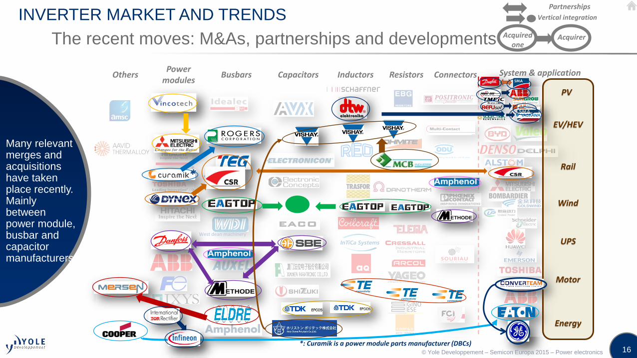
The recent moves: M&As, partnerships and developments
Many relevant merges and acquisitions have taken place recently. Mainly between power module, busbar and capacitor manufacturers
West dean machinery
*
*: Curamik is a power module parts manufacturer (DBCs)
Busbars Capacitors Inductors ResistorsOthers ConnectorsPower
modulesSystem & application
*
PV
EV/HEV
Rail
Wind
UPS
Motor
Energy
*
Acquirer
Partnerships
Vertical integration
Acquired one
© Yole Developpement – Semicon Europa 2015 – Power electronics
18
POWER PACKAGING MARKET AND TRENDS
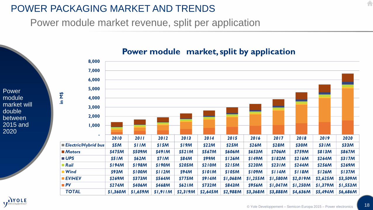
Power module market revenue, split per application
Power module market will double between 2015 and 2020
© Yole Developpement – Semicon Europa 2015 – Power electronics

19
POWER PACKAGING MARKET AND TRENDS
What is power module packaging?
• Power module with baseplate is the standard design (70 to 80% of available power modules). DBC (Direct Bond Copper)packaging is the most widespread packaging. These modules are complex and expensive.
• Common failure in a power module is caused by thermal cycling. Mismatching CTE (coefficient of thermal expansion) canmake layers detach from one another. Some gel filling also cannot handle high temperatures.
Modules are used in every industrial application with high power and each part require innovation
Heatsink
Thermal grease
Substrate
SBD IGBT
Baseplate
DBC
Busbar connection
Solder
Copper metallization
Plastic case
Die attach
Interconnection
Gel filling
Substrate attach
In orange: Common failure
locations © Yole Developpement – Semicon Europa 2015 – Power electronics

20
POWER PACKAGING MARKET AND TRENDS
Which evolution for each part of modules?
Both materials and designs are evolving in power modules
2015 2020 2025…2018
Standard
baseplateBaseplate
Double side
coolingPin-fin
baseplate
Micro-channel
cooling
No
baseplate?
TIMThermal
greasePCM
Which
evolution for
TIM?
Removal?
Substrate
DBC
AMB
Leadframe Single/double
layer
No substrate?
Die attach
Sn
soldering
TLPS Silver (paste/film) sintering
AuSn/AuGe
Brazing
Encapsulation
Silicon gel Epoxy resin
Silicon gel/
epoxy resin high
temperature
New materials
such as
parylene
Interconnections
Al wire
bonding
Ribbon
bonding
Cu wire
bonding
‘‘ Top side’’
bonding Ball
bonding
© Yole Developpement – Semicon Europa 2015 – Power electronics

21
POWER PACKAGING MARKET AND TRENDS
Roadmap of power module packaging design
In the future power modules will be entirely reshaped, with changes done depending on the power targeted
Bosch example• Molded package• Double side soldering• Low inductance
Mitsubishi example• Six Pack IGBT/Diode Package• Cooling fin• Thick copper layer for thermal
spreading• Direct substrate cooling
Mid-power modulesDesign evolution
Die on heatsink• Die attach: film
sintering? Gold sintering? Glue? Silver oxalate?
• Ceramic heatsink?• Ball bonding?
2018
2020
2014
2025
• Wide use of leadframe• Over-molded package• Top interconnections• Ag sintering for die attach
• Encapsulation with parylene• Ribbon bonding• Silver (Ag) sintering for die
attach• Pin-fin baseplate
© Yole Developpement – Semicon Europa 2015 – Power electronics

22
POWER PACKAGING MARKET AND TRENDS
Reliability and cost are the two main drivers for evolution
Depending on the level of reliability needed power modules need to be optimized or not
Reliabilit
y
Cost
pressure
Currently
widesprea
dIn expansion
phase
In
development
phase
Thermal
grease
Soldering
for die
attachDie on
leadfram
e
Ag sintering
for die
attach
Ball
bonding
Al
wirebonding
Parylene for
encapsulatio
n
Silicone gel
encapsulatio
n Over-
molded PM
Ribbon
bonding
Pin-fin
baseplat
e
Cu
wirebondin
g
Double
side
cooling
DBC
substrate
AMB
substrat
e
Micro-
channel
cooling
PCM
Gold
alloys
soldering
AlN
ceramic
Al2O3
cerami
c
Si3N4
ceramic
© Yole Developpement – Semicon Europa 2015 – Power electronics

23
POWER PACKAGING MARKET AND TRENDS
What evolution for discrete devices packaging?
Key drivers for discretes are the same as for power modules: Efficiency and power density increase
• Discrete components packaging evolution is motivated by the same reasons as power modules:
• Miniaturization
• Power density increase
• Yield/Efficiency increase
Time
PackageSize
2000 2010Before 2000 2020
~ mm
~ 10mm
~
100mm
~ cm
© Yole Developpement – Semicon Europa 2015 – Power electronics

24
POWER PACKAGING MARKET AND TRENDS
GaNPXproduct is considered as a trendsetter for WBG packaging
• During PCIM 2014 conference, AT&S and GaN Systems companies presented their newpackage solution for GaN devices: GaNPX
• 100V/60A in 5x5mm
• This device is one of the first ones to take into account WBG specificities in an efficientpackage: Die is embedded at substrate level
• GaN devices focus is a good strategy:• Planarity of devices (easier integration)
• Needs for good heat management
• Promising future market
Sources: GaN Systems/AT&S and Yole’s report
“GaN System GS66508P 650V 30A 52mohm GaN
on Si HEMT normally-off transistor”
• Yole expects GaNPX package to inspire the way
for future WBG semiconductors packaging
WBG semiconductors packaging case study: GaN Systems and AT&S GaNPX
© Yole Developpement – Semicon Europa 2015 – Power electronics
25
POWER PACKAGING MARKET AND TRENDS
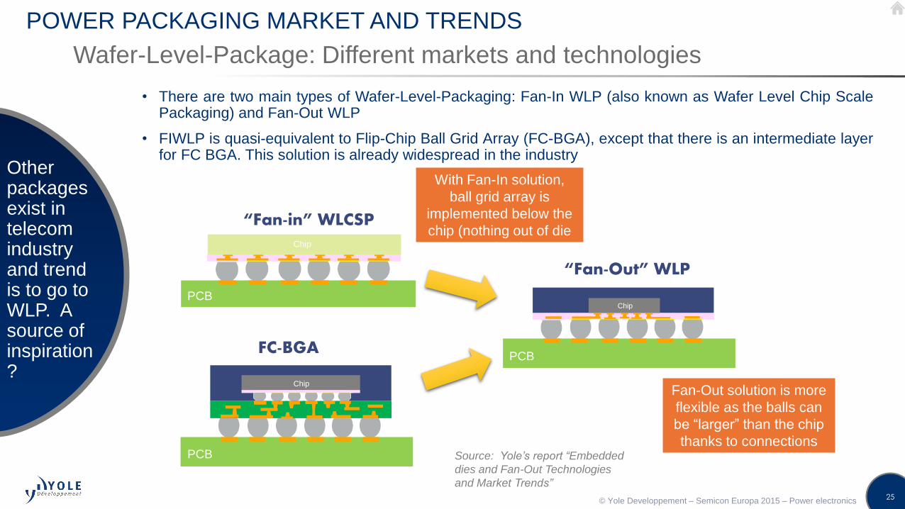
Wafer-Level-Package: Different markets and technologies
Other packages exist in telecom industry and trend is to go to WLP. A source of inspiration?
• There are two main types of Wafer-Level-Packaging: Fan-In WLP (also known as Wafer Level Chip ScalePackaging) and Fan-Out WLP
• FIWLP is quasi-equivalent to Flip-Chip Ball Grid Array (FC-BGA), except that there is an intermediate layerfor FC BGA. This solution is already widespread in the industry
PCB
Chip
“Fan-in” WLCSP
PCB
Chip
“Fan-Out” WLP
PCB
Chip
FC-BGA
With Fan-In solution,
ball grid array is
implemented below the
chip (nothing out of die
surface)
Fan-Out solution is more
flexible as the balls can
be “larger” than the chip
thanks to connectionsSource: Yole’s report “Embedded
dies and Fan-Out Technologies
and Market Trends”
© Yole Developpement – Semicon Europa 2015 – Power electronics

© 2015
Semiconductor DevicesOpportunities for Wide Band Gap (WBG)

27
SEMICONDUCTOR DEVICES: OPPORTUNITIES FOR WIDE BAND GAP
Life–Cycle of Power Device Technologies
A new generation every ~20 years…
Bip
ola
rU
nip
ola
rFi
eld
Eff
ect
Tra
nsi
sto
rs
DiodeGTO
Thyristor
BJT
IGCT
1970 1990 2020
IGBT
SiC BJT
SJMOSFET
SiliconSiC
GaN
Gen. 2Max. 600V
Gen. 6Max. 6500V
…
SiC JFET
GaN HEMT
MOSFET
2015
Thyristor & MOSFET era Si IGBT era WBG era??
SiC MOSFETSiC diode
© Yole Developpement – Semicon Europa 2015 – Power electronics
28
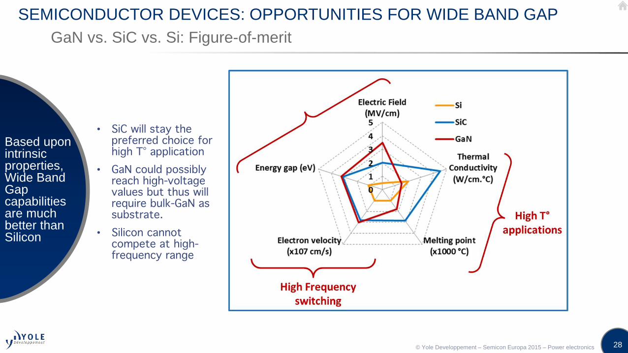
SEMICONDUCTOR DEVICES: OPPORTUNITIES FOR WIDE BAND GAP
GaN vs. SiC vs. Si: Figure-of-merit
• SiC will stay the preferred choice for high T° application
• GaN could possibly reach high-voltage values but thus will require bulk-GaN as substrate.
• Silicon cannot compete at high-frequency range
Based uponintrinsicproperties, Wide Band Gap capabilitiesare muchbetter thanSilicon
© Yole Developpement – Semicon Europa 2015 – Power electronics

29
SEMICONDUCTOR DEVICES: OPPORTUNITIES FOR WIDE BAND GAP
Reasons for Wide Band Gap devices added value
High electron mobility and high junction temperature are the key characteristics
High electron mobilityHigh Junction T°
No recovery time
during switching
Low lossesless energy to dissipate
Fewer cooling
needs
System size
and weight
reduction
High switching
frequency
Smaller filters
and passives
Intrinsic
properties
Impact on
operation
Impact on
power module
Impact on
power system
© Yole Developpement – Semicon Europa 2015 – Power electronics

30
SEMICONDUCTOR DEVICES: OPPORTUNITIES FOR WIDE BAND GAP
Power device technology positioning and evolution
WBG devices are primarily positioned in high-end applications and have potential in automotive
1200V or more600V or less
Pro
du
ct r
ange
Voltage
IGBTThyristor
IGCT…
SiC
MOSFET
Triacs
Bipolar…
3.3kV and more200V
GaN GaN Yole Développement - December 2014
• Historically, silicon had the complete monopoly of the semiconductors industry in Integrated Circuits (IC), in Microchips and in Power Electronics.
• New raw materials for semiconductors such as Silicon Carbide (SiC) and Gallium Nitride (GaN) have been developed for some decades now.
© Yole Developpement – Semicon Europa 2015 – Power electronics
31
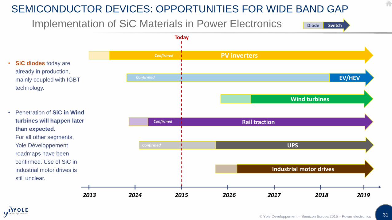
SEMICONDUCTOR DEVICES: OPPORTUNITIES FOR WIDE BAND GAP
Implementation of SiC Materials in Power Electronics
• SiC diodes today are
already in production,
mainly coupled with IGBT
technology.
• Penetration of SiC in Wind
turbines will happen later
than expected.
For all other segments,
Yole Développement
roadmaps have been
confirmed. Use of SiC in
industrial motor drives is
still unclear.
2013 2014 2015 2016 2017 2018 2019
Industrial motor drives
UPS
Rail traction
Wind turbines
EV/HEV
PV inverters
Confirmed
Confirmed
Confirmed
Today
Confirmed
Diode Switch
© Yole Developpement – Semicon Europa 2015 – Power electronics

32
SEMICONDUCTOR DEVICES: OPPORTUNITIES FOR WIDE BAND GAP
Implementation of GaN Materials in Power Electronics
• Characteristics of GaN-based
inverters will be:
• They will primarily target medium voltage
applications (in the 200 – 600V range)
• GaN targeted applications will be very
different from SiC, at first. We will
observe a competition in PV inverters, and
potentially, both technologies will be used.
For the EV/HEV, GaN devices will first enter
the DC/DC converters and the chargers, but
not the power train inverter.
• GaN devices are excluded from high-
voltage applications such as wind turbines
and rail traction.
2013 2014 2015 2016 2017 2018 2019
Industrial motor drives
UPS
Rail traction
Wind turbine
EV/HEV
PV inverters
PFC/Power supplies
Small DC/DC converters / Wireless chargers
Today
Confirmed
© Yole Developpement – Semicon Europa 2015 – Power electronics

34
CONCLUSIONS
• 21st century challenges are leading to new needs, new drivers,new opportunities
• To face these evolutions power electronics industry will reshapeitself to meet specific application requirements
• Power density• Overall system weight• Efficiency improvement
• Technical breakthrough are expected at each level of the valuechain:
• System architectures and topologies• Packaging• Semiconductor devices
© Yole Developpement – Semicon Europa 2015 – Power electronics
36
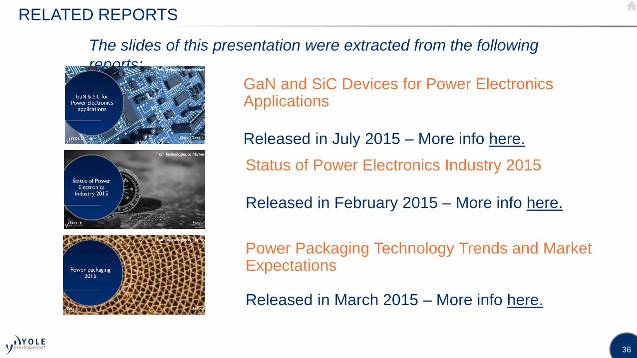
RELATED REPORTS
GaN and SiC Devices for Power Electronics Applications
Released in July 2015 – More info here.
The slides of this presentation were extracted from the following
reports:
Status of Power Electronics Industry 2015
Released in February 2015 – More info here.
Power Packaging Technology Trends and Market Expectations
Released in March 2015 – More info here.
37
ABOUT THE AUTHORS
Biography & contact
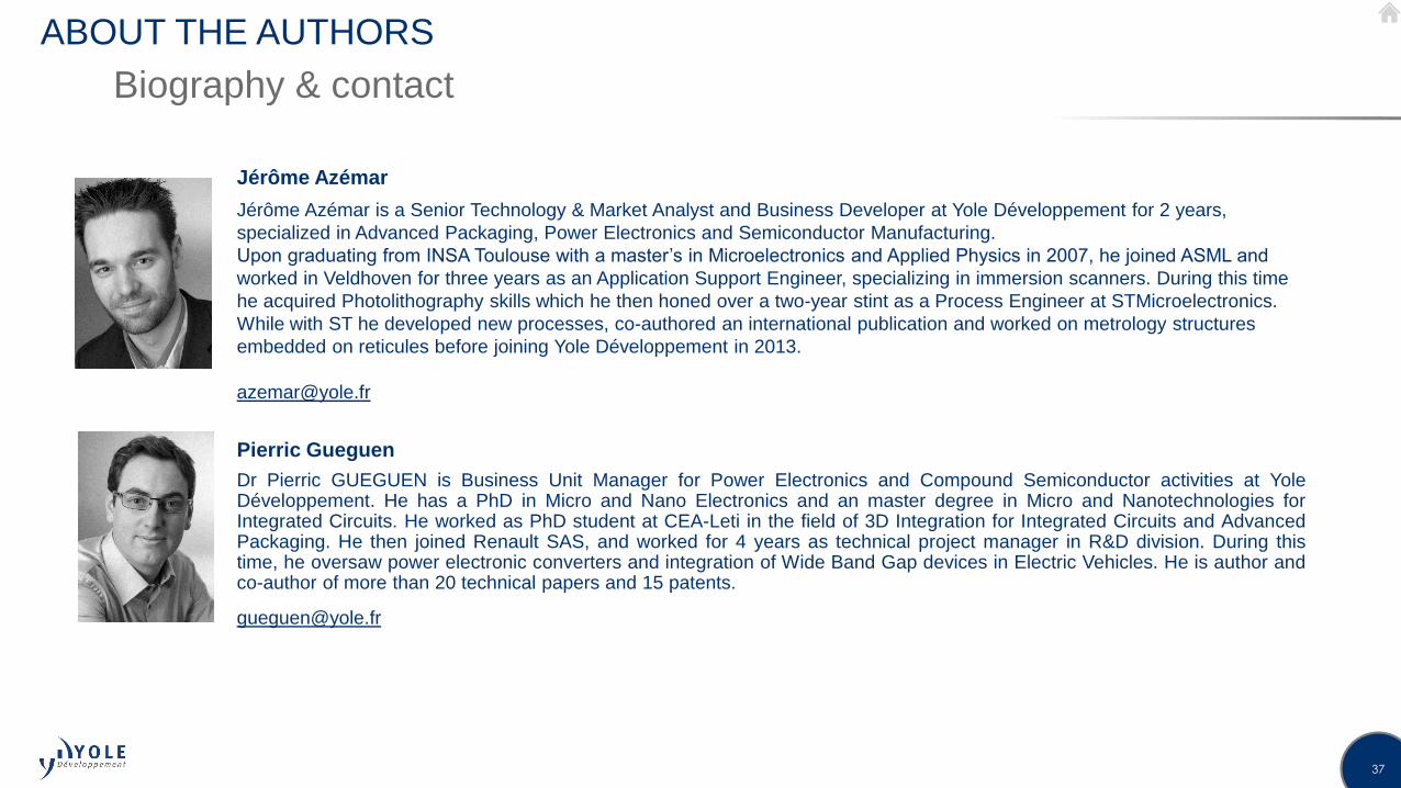
Pierric Gueguen
Dr Pierric GUEGUEN is Business Unit Manager for Power Electronics and Compound Semiconductor activities at YoleDéveloppement. He has a PhD in Micro and Nano Electronics and an master degree in Micro and Nanotechnologies forIntegrated Circuits. He worked as PhD student at CEA-Leti in the field of 3D Integration for Integrated Circuits and AdvancedPackaging. He then joined Renault SAS, and worked for 4 years as technical project manager in R&D division. During thistime, he oversaw power electronic converters and integration of Wide Band Gap devices in Electric Vehicles. He is author andco-author of more than 20 technical papers and 15 patents.
Jérôme Azémar
Jérôme Azémar is a Senior Technology & Market Analyst and Business Developer at Yole Développement for 2 years,
specialized in Advanced Packaging, Power Electronics and Semiconductor Manufacturing.
Upon graduating from INSA Toulouse with a master’s in Microelectronics and Applied Physics in 2007, he joined ASML and
worked in Veldhoven for three years as an Application Support Engineer, specializing in immersion scanners. During this time
he acquired Photolithography skills which he then honed over a two-year stint as a Process Engineer at STMicroelectronics.
While with ST he developed new processes, co-authored an international publication and worked on metrology structures
embedded on reticules before joining Yole Développement in 2013.
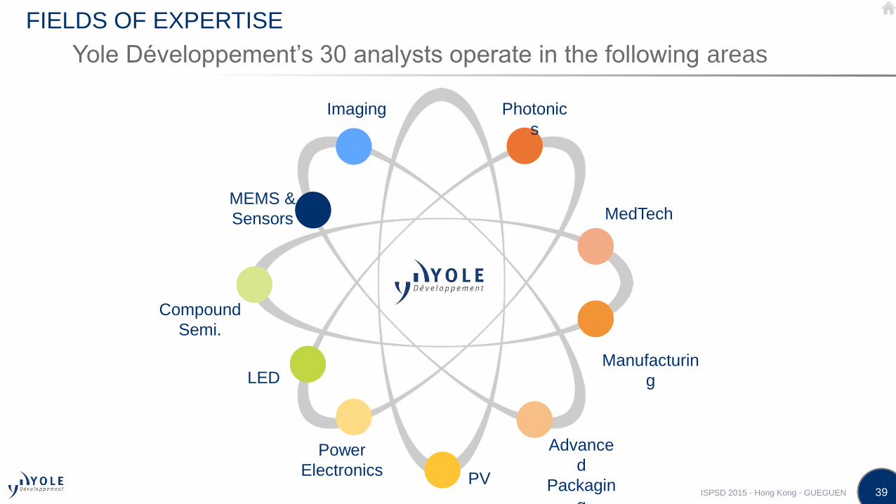
39
MEMS &
Sensors
LED
Compound
Semi.
Imaging Photonic
s
MedTech
Manufacturin
g
Advance
d
Packagin
g
PV
Power
Electronics
FIELDS OF EXPERTISE
Yole Développement’s 30 analysts operate in the following areas
ISPSD 2015 - Hong Kong - GUEGUEN
40
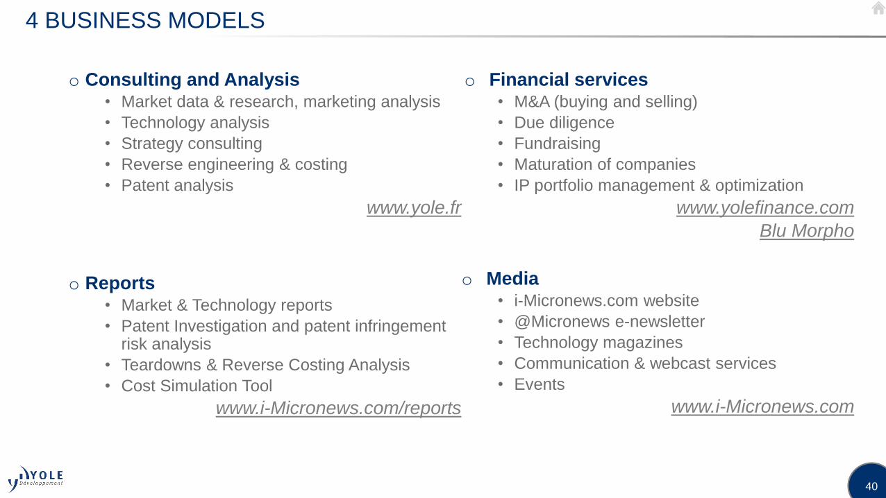
4 BUSINESS MODELS
o Consulting and Analysis• Market data & research, marketing analysis
• Technology analysis
• Strategy consulting
• Reverse engineering & costing
• Patent analysis
www.yole.fr
o Reports• Market & Technology reports
• Patent Investigation and patent infringement risk analysis
• Teardowns & Reverse Costing Analysis
• Cost Simulation Tool
www.i-Micronews.com/reports
o Financial services• M&A (buying and selling)
• Due diligence
• Fundraising
• Maturation of companies
• IP portfolio management & optimization
www.yolefinance.com
Blu Morpho
o Media• i-Micronews.com website
• @Micronews e-newsletter
• Technology magazines
• Communication & webcast services
• Events
www.i-Micronews.com

41
A GROUP OF COMPANIES
Market,
technology and
strategy
consulting
www.yole.fr
M&A operations
Due diligences
www.yolefinance.com
Fundraising
Maturation of companies
IP portfolio management &
optimization
www.bmorpho.com
Manufacturing costs analysis
Teardown and reverse engineering
Cost simulation tools
www.systemplus.fr
IP analysis
Patent
assessment
www.knowmade.fr
ISPSD 2015 - Hong Kong - GUEGUEN
42
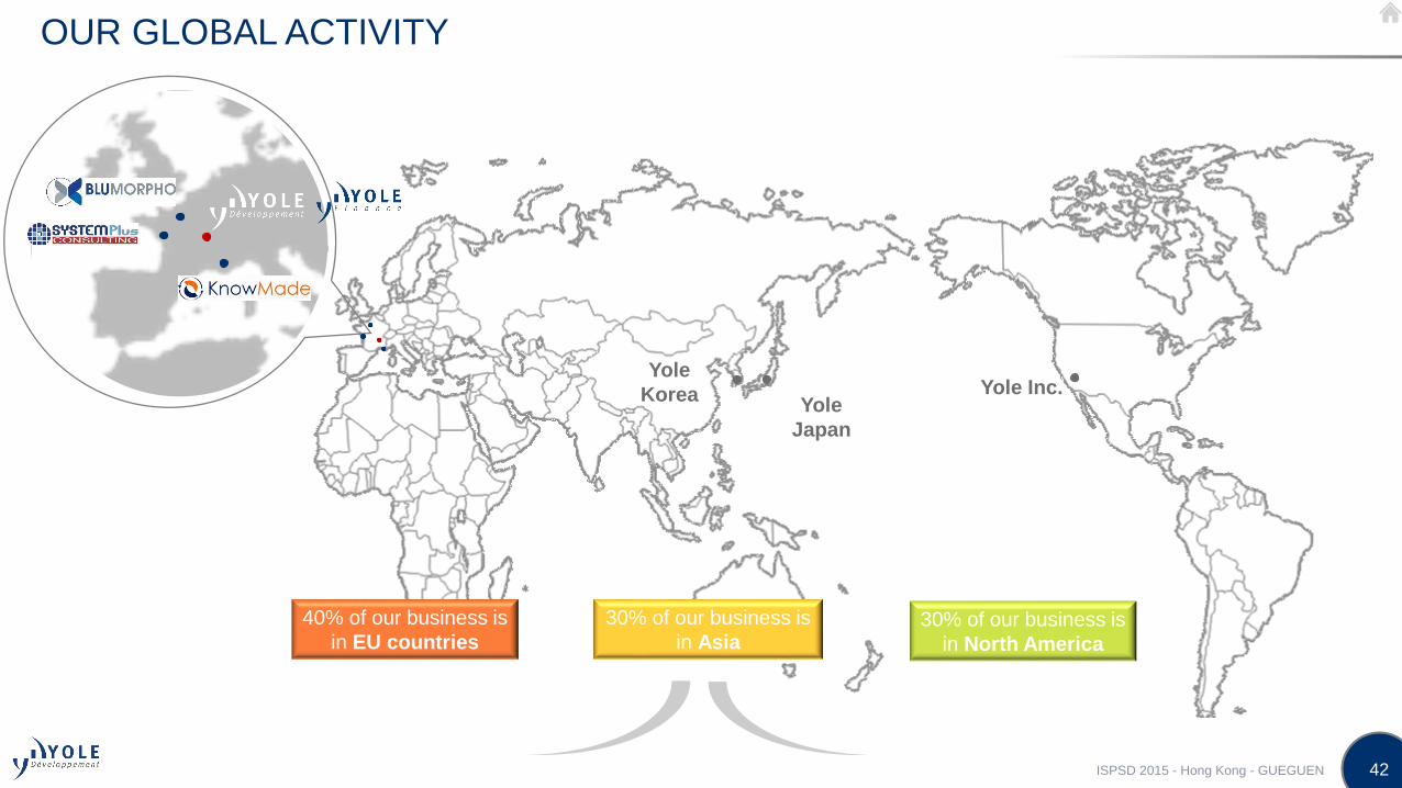
OUR GLOBAL ACTIVITY
Yole
Japan
Yole Inc.Yole
Korea
40% of our business is
in EU countries30% of our business is
in North America
30% of our business is
in Asia
ISPSD 2015 - Hong Kong - GUEGUEN

43
SERVING THE ENTIRE SUPPLY CHAIN
Our analysts provide market
analysis, technology evaluation,
and business plan along the entire
supply chain
Integrators and
end-users
Device
makers
Suppliers: material,
equipment, OSAT,
foundries…
Financial
investors,
R&D centers
ISPSD 2015 - Hong Kong - GUEGUEN

44
CONTACT INFORMATION
o Consulting and Specific Analysis
• North America: Steve LaFerriere, Director of Northern America Business Development, Yole Inc.Email: [email protected]
• Japan: Yutaka Katano, General Manager, Yole Japan & President, Yole K.K.Email: [email protected]
• EMEA: Jerome Azemar, Senior Analyst and Business Development Manager, Yole DéveloppementEmail: [email protected]
• RoW: Jean-Christophe Eloy, President & CEO, Yole DéveloppementEmail: [email protected]
o Report business
• North America: Steve LaFerriere, Director of Northern America Business Development, Yole Inc.Email: [email protected]
• EMEA: Jerome Azemar, Senior Analyst and Business Development Manager, Yole DéveloppementEmail: [email protected]
• Japan & Asia: Takashi Onozawa, Sales Asia & General Manager, Yole K.K.Email: [email protected]
• Korea: Hailey Yang, Business Development Manager, Korean OfficeEmail: [email protected]
o Financial services
• Jean-Christophe Eloy, CEO & PresidentEmail: [email protected]
Follow us on