Embed Size (px)
Citation preview
www.bookspar.com | Website for Students | VTU NOTES | QUESTION PAPERS | NEWS | RESULTS
www.bookspar.com | Website for Students | VTU NOTES | QUESTION PAPERS | NEWS | RESULTS
Power Amplifiers
• Introduction
• Definitions and amplifier types
• Series fed class A amplifiers
• Transformer coupled class A amplifier
• Transformer coupled amplifier continuation
• Numerical
• Class B amplifier operation
• Class B amplifier circuits
• Numerical
• Amplifier distortion
• Numerical
• Second harmonic distortion
• Power transistor heat sinking
• Thermal analogy of power transistor
• Class C and class D amplifiers
• Numerical
Introduction Amplifier receives a signal from some pickup transducer or other input
source and provides larger version of the signal.
www.bookspar.com | Website for Students | VTU NOTES | QUESTION PAPERS | NEWS | RESULTS
www.bookspar.com | Website for Students | VTU NOTES | QUESTION PAPERS | NEWS | RESULTS
In small signal amplifiers the main factors are usually amplification,
linearity and magnitude of gain.
Classes of PAs
Amplifier classes represent the amount the output signal varies over one
cycle of operation for a full cycle of input signal
So the following classes of PA are defined
Class A
Class B
Class AB
Class C
Class D
Class A amplifier
• Class A amplifying devices operate over the whole of the input cycle such
that the output signal is an exact scaled-up replica of the input with no
clipping. Class A amplifiers are the usual means of implementing small-
signal amplifiers. They are not very efficient. a theoretical maximum of 50%
is obtainable with inductive output coupling and only 25% with capacitive
coupling.
• In a Class A circuit, the amplifying element is biased so the device is always
conducting to some extent, and is operated over the most linear portion of its
characteristic curve Because the device is always conducting, even if there is
no input at all, power is drawn from the power supply. This is the chief
reason for its inefficiency.

www.bookspar.com | Website for Students | VTU NOTES | QUESTION PAPERS | NEWS | RESULTS
www.bookspar.com | Website for Students | VTU NOTES | QUESTION PAPERS | NEWS | RESULTS
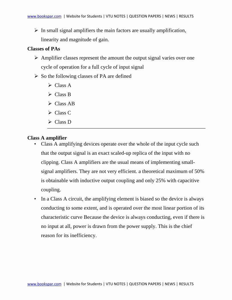
Class B
• Class B amplifiers only amplify half of the input wave cycle. As such they
create a large amount of distortion, but their efficiency is greatly improved
and is much better than Class A. Class B has a maximum theoretical
efficiency of 78.5% (i.e., π/4). This is because the amplifying element is
switched off altogether half of the time, and so cannot dissipate power.
• A single Class B element is rarely found in practice, though it can be used in
RF power amplifier where the distortion levels are less important. However
Class C is more commonly used for this.
www.bookspar.com | Website for Students | VTU NOTES | QUESTION PAPERS | NEWS | RESULTS
www.bookspar.com | Website for Students | VTU NOTES | QUESTION PAPERS | NEWS | RESULTS
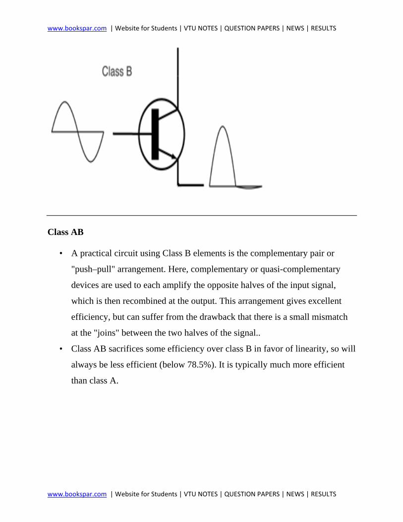
Class AB
• A practical circuit using Class B elements is the complementary pair or
"push–pull" arrangement. Here, complementary or quasi-complementary
devices are used to each amplify the opposite halves of the input signal,
which is then recombined at the output. This arrangement gives excellent
efficiency, but can suffer from the drawback that there is a small mismatch
at the "joins" between the two halves of the signal..
• Class AB sacrifices some efficiency over class B in favor of linearity, so will
always be less efficient (below 78.5%). It is typically much more efficient
than class A.
www.bookspar.com | Website for Students | VTU NOTES | QUESTION PAPERS | NEWS | RESULTS
www.bookspar.com | Website for Students | VTU NOTES | QUESTION PAPERS | NEWS | RESULTS
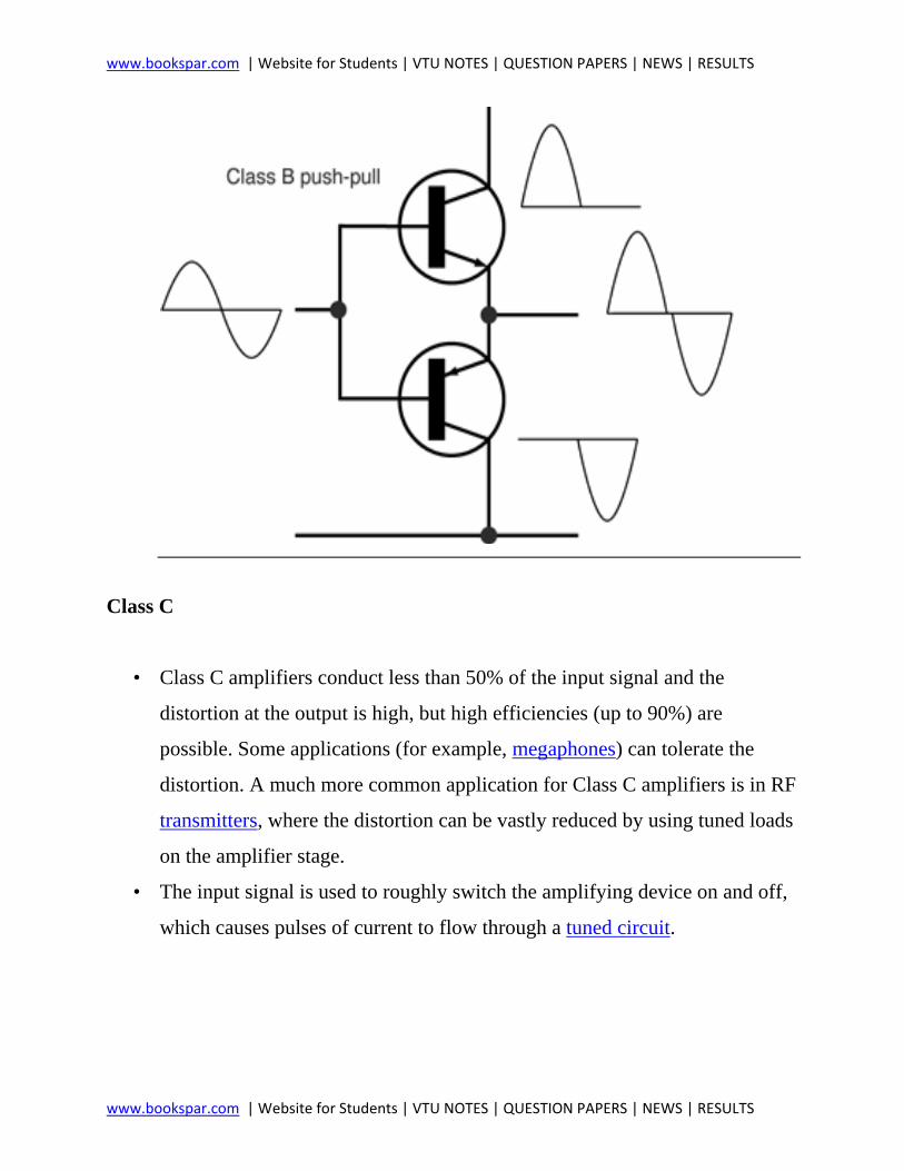
Class C
• Class C amplifiers conduct less than 50% of the input signal and the
distortion at the output is high, but high efficiencies (up to 90%) are
possible. Some applications (for example, megaphones) can tolerate the
distortion. A much more common application for Class C amplifiers is in RF
transmitters, where the distortion can be vastly reduced by using tuned loads
on the amplifier stage.
• The input signal is used to roughly switch the amplifying device on and off,
which causes pulses of current to flow through a tuned circuit.
www.bookspar.com | Website for Students | VTU NOTES | QUESTION PAPERS | NEWS | RESULTS
www.bookspar.com | Website for Students | VTU NOTES | QUESTION PAPERS | NEWS | RESULTS
Class D
• Class D amplifiers are much more efficient than Class AB power amplifiers.
As such, Class D amplifiers do not need large transformers and heavy
heatsinks, which means that they are smaller and lighter in weight than an
equivalent Class AB amplifier. All power devices in a Class D amplifier are
operated in on/off mode.
• These amplifiers use pulse width modulation,
www.bookspar.com | Website for Students | VTU NOTES | QUESTION PAPERS | NEWS | RESULTS
www.bookspar.com | Website for Students | VTU NOTES | QUESTION PAPERS | NEWS | RESULTS
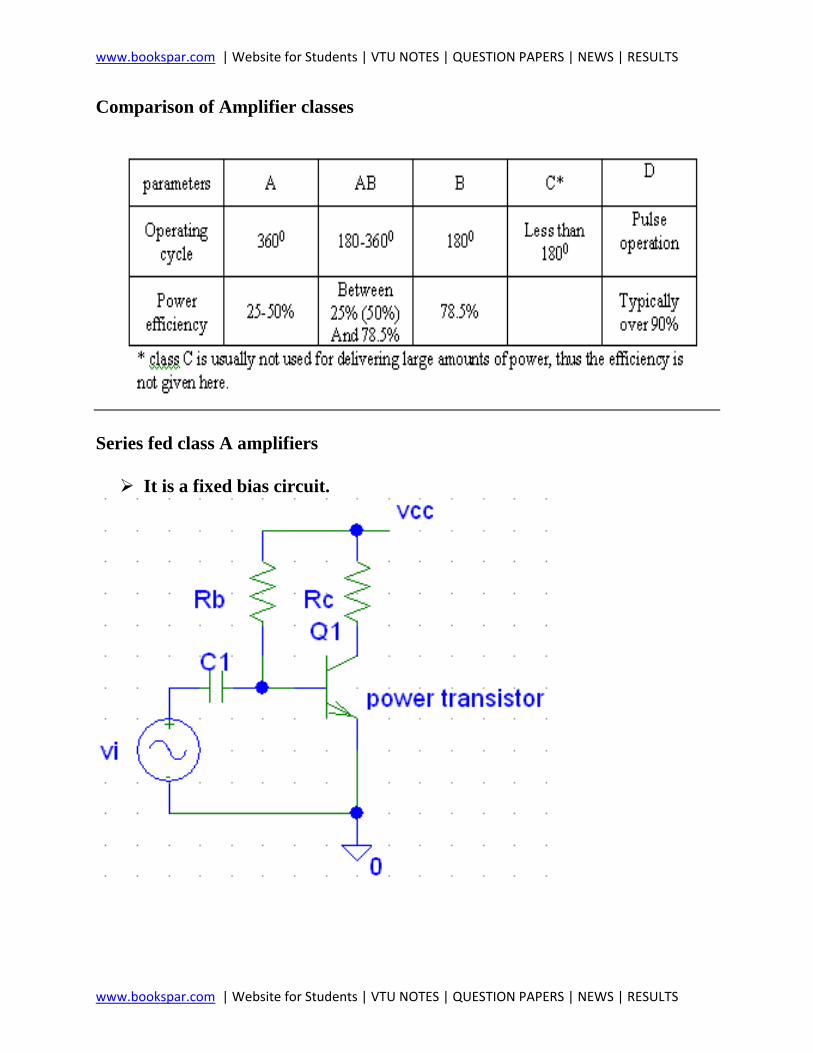
Comparison of Amplifier classes
Series fed class A amplifiers It is a fixed bias circuit.
www.bookspar.com | Website for Students | VTU NOTES | QUESTION PAPERS | NEWS | RESULTS
www.bookspar.com | Website for Students | VTU NOTES | QUESTION PAPERS | NEWS | RESULTS
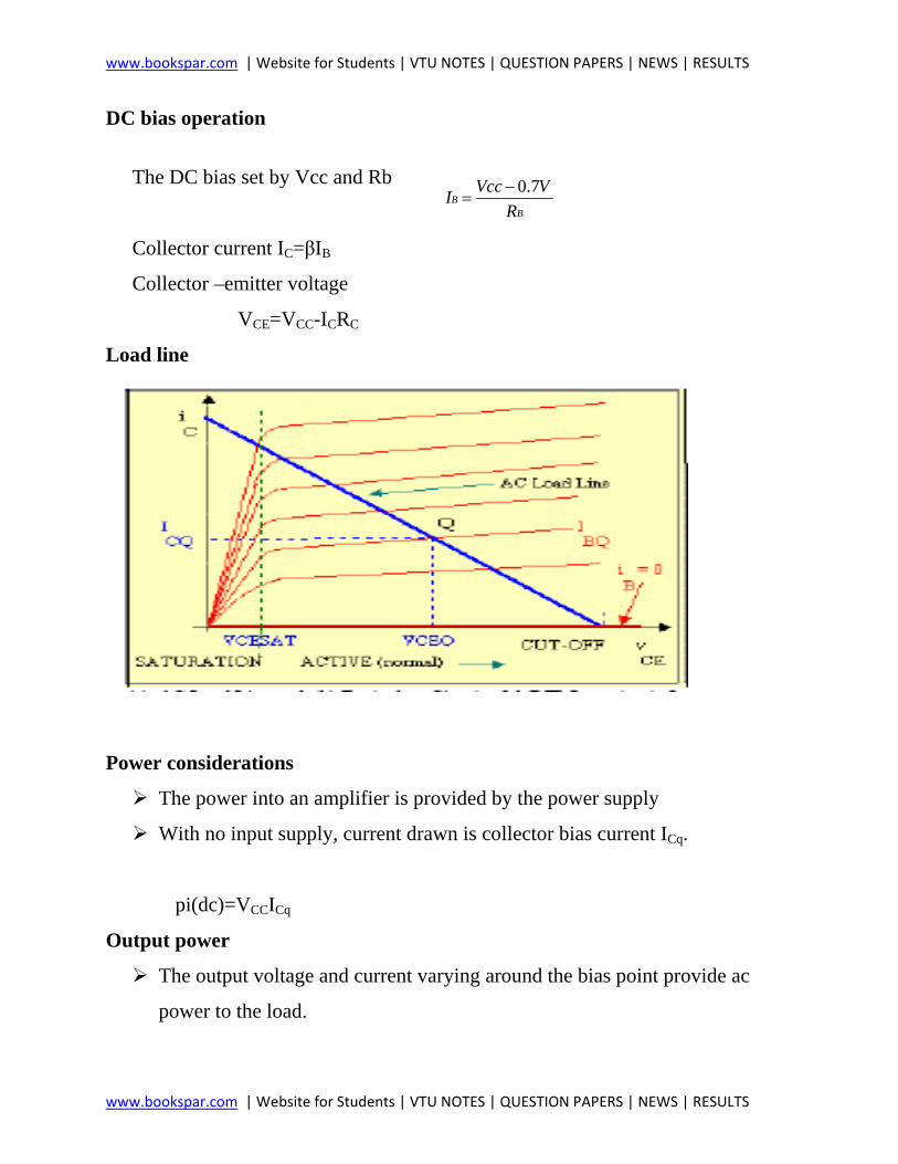
DC bias operation
The DC bias set by Vcc and Rb
Collector current IC=βIB
Collector –emitter voltage
VCE=VCC-ICRC
Load line
Power considerations
The power into an amplifier is provided by the power supply
With no input supply, current drawn is collector bias current ICq.
pi(dc)=VCCICq
Output power
The output voltage and current varying around the bias point provide ac
power to the load.
BB
RVVccI 7.0−
=
www.bookspar.com | Website for Students | VTU NOTES | QUESTION PAPERS | NEWS | RESULTS
www.bookspar.com | Website for Students | VTU NOTES | QUESTION PAPERS | NEWS | RESULTS
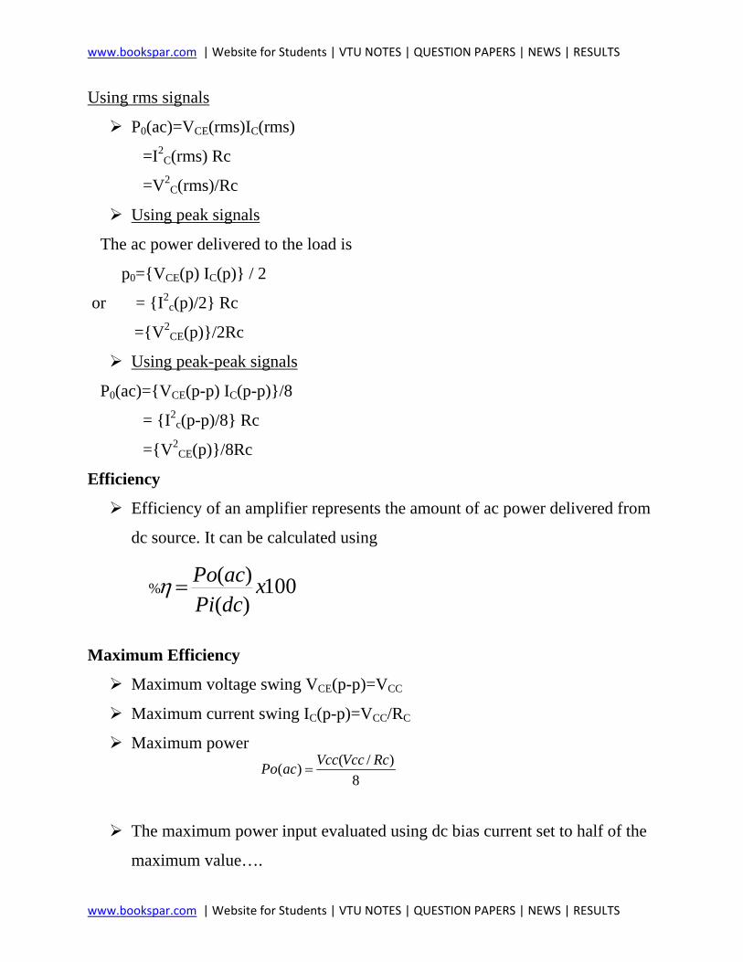
Using rms signals
P0(ac)=VCE(rms)IC(rms)
=I2C(rms) Rc
=V2C(rms)/Rc
Using peak signals
The ac power delivered to the load is
p0={VCE(p) IC(p)} / 2
or = {I2c(p)/2} Rc
={V2CE(p)}/2Rc
Using peak-peak signals
P0(ac)={VCE(p-p) IC(p-p)}/8
= {I2c(p-p)/8} Rc
={V2CE(p)}/8Rc
Efficiency
Efficiency of an amplifier represents the amount of ac power delivered from
dc source. It can be calculated using
Maximum Efficiency
Maximum voltage swing VCE(p-p)=VCC
Maximum current swing IC(p-p)=VCC/RC
Maximum power
The maximum power input evaluated using dc bias current set to half of the
maximum value….
100)()(
% xdcPiacPo=η
8)/()( RcVccVccacPo =
www.bookspar.com | Website for Students | VTU NOTES | QUESTION PAPERS | NEWS | RESULTS
www.bookspar.com | Website for Students | VTU NOTES | QUESTION PAPERS | NEWS | RESULTS
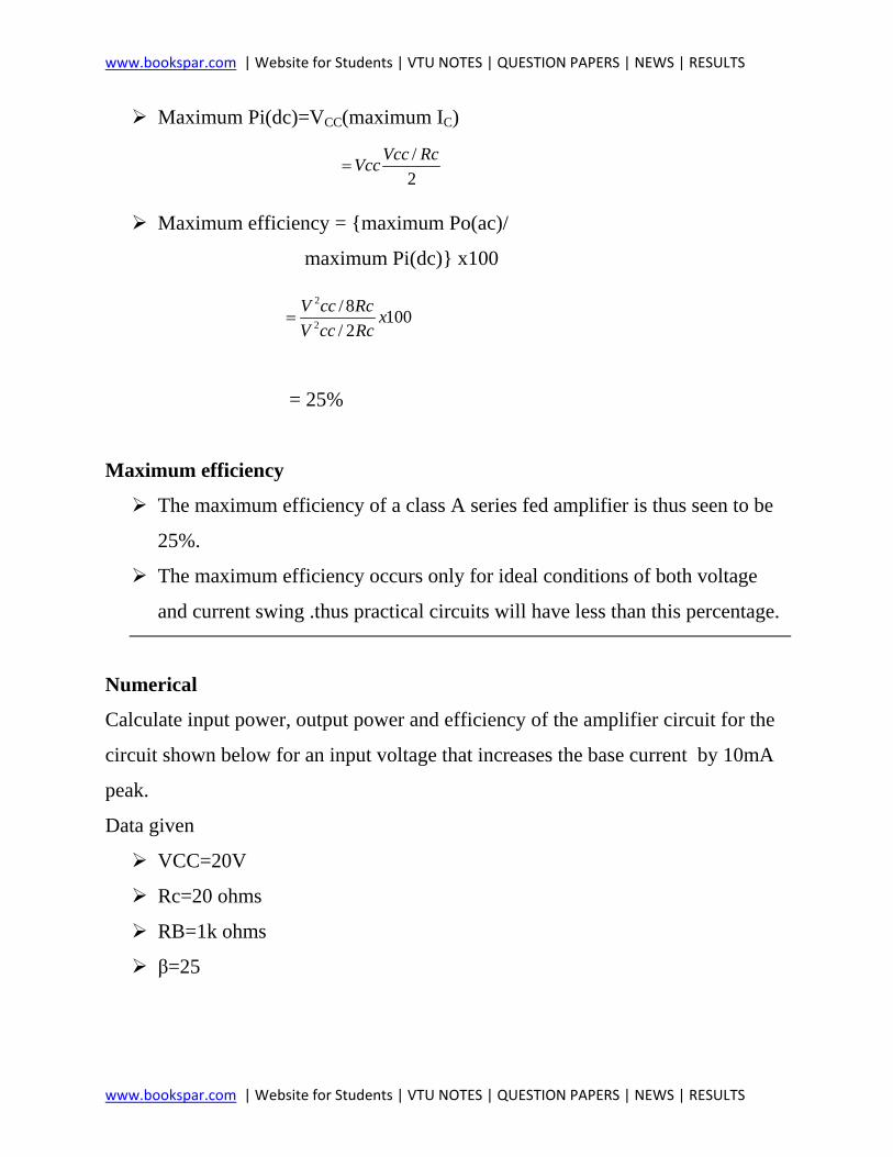
Maximum Pi(dc)=VCC(maximum IC)
Maximum efficiency = {maximum Po(ac)/
maximum Pi(dc)} x100
= 25%
Maximum efficiency
The maximum efficiency of a class A series fed amplifier is thus seen to be
25%.
The maximum efficiency occurs only for ideal conditions of both voltage
and current swing .thus practical circuits will have less than this percentage.
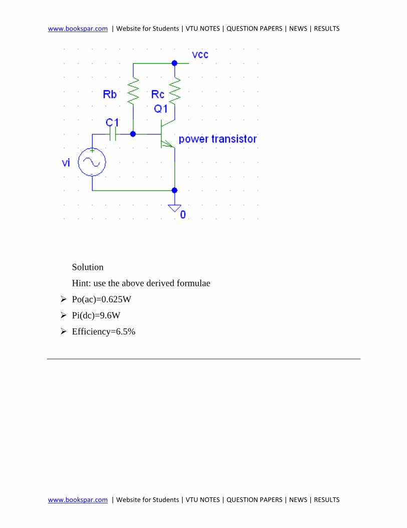
Numerical
Calculate input power, output power and efficiency of the amplifier circuit for the
circuit shown below for an input voltage that increases the base current by 10mA
peak.
Data given
VCC=20V
Rc=20 ohms
RB=1k ohms
β=25
2/ RcVccVcc=
1002/8/
2
2
xRcccVRcccV
=
www.bookspar.com | Website for Students | VTU NOTES | QUESTION PAPERS | NEWS | RESULTS
www.bookspar.com | Website for Students | VTU NOTES | QUESTION PAPERS | NEWS | RESULTS
Solution
Hint: use the above derived formulae
Po(ac)=0.625W
Pi(dc)=9.6W
Efficiency=6.5%
www.bookspar.com | Website for Students | VTU NOTES | QUESTION PAPERS | NEWS | RESULTS
www.bookspar.com | Website for Students | VTU NOTES | QUESTION PAPERS | NEWS | RESULTS
Transformer coupled class A amplifier
The transformer can step up or step down a voltage applied to primary coil .
Transformer coupled class A PA • A form of class A amplifier having maximum efficiency of 50% uses
transformer to couple the output signal to the load. Impedance transformation
If α=N1/N2 Then Above equation reduces to
12
12
NN
VV
=21
12
NN
II
=
2
1 12
12
12
21
22
1/12/2
12
=====
NN
NN
NN
II
IV
IVIV
RR
RLRL
221
21
21 α=
==
NN
RR
RLRL
www.bookspar.com | Website for Students | VTU NOTES | QUESTION PAPERS | NEWS | RESULTS
www.bookspar.com | Website for Students | VTU NOTES | QUESTION PAPERS | NEWS | RESULTS
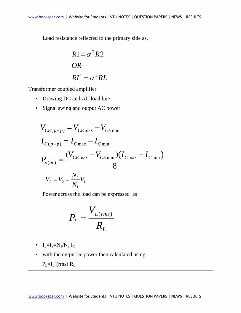
Load resistance reflected to the primary side as,
Transformer coupled amplifier
• Drawing DC and AC load line
• Signal swing and output AC power
Power across the load can be expressed as
• IL=I2=N1/N2 IC
• with the output ac power then calculated using
PL=IL2(rms) RL
RLRLOR
RR
21
2 21
α
α
=
=
8))(( minmaxminmax
)(
minmax)(
minmax)(
CCCECEaco
CCppC
CECEppCE
IIVVP
IIIVVV
−−=
−=
−=
−
−
11
22 V
NNVVL ==
L
rmsLL R
VP )(=
www.bookspar.com | Website for Students | VTU NOTES | QUESTION PAPERS | NEWS | RESULTS
www.bookspar.com | Website for Students | VTU NOTES | QUESTION PAPERS | NEWS | RESULTS
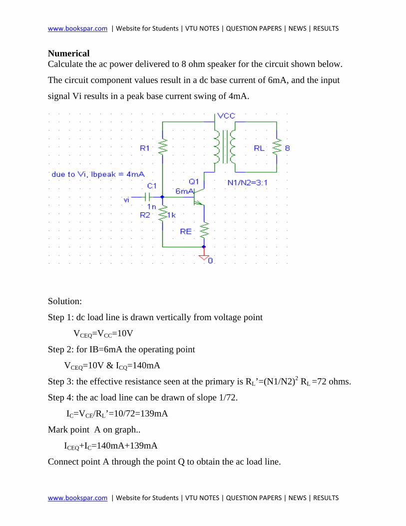
Numerical Calculate the ac power delivered to 8 ohm speaker for the circuit shown below.
The circuit component values result in a dc base current of 6mA, and the input
signal Vi results in a peak base current swing of 4mA.
Solution:
Step 1: dc load line is drawn vertically from voltage point
VCEQ=VCC=10V
Step 2: for IB=6mA the operating point
VCEQ=10V & ICQ=140mA
Step 3: the effective resistance seen at the primary is RL’=(N1/N2)2 RL =72 ohms.
Step 4: the ac load line can be drawn of slope 1/72.
IC=VCE/RL’=10/72=139mA
Mark point A on graph..
ICEQ+IC=140mA+139mA
Connect point A through the point Q to obtain the ac load line.
www.bookspar.com | Website for Students | VTU NOTES | QUESTION PAPERS | NEWS | RESULTS
www.bookspar.com | Website for Students | VTU NOTES | QUESTION PAPERS | NEWS | RESULTS
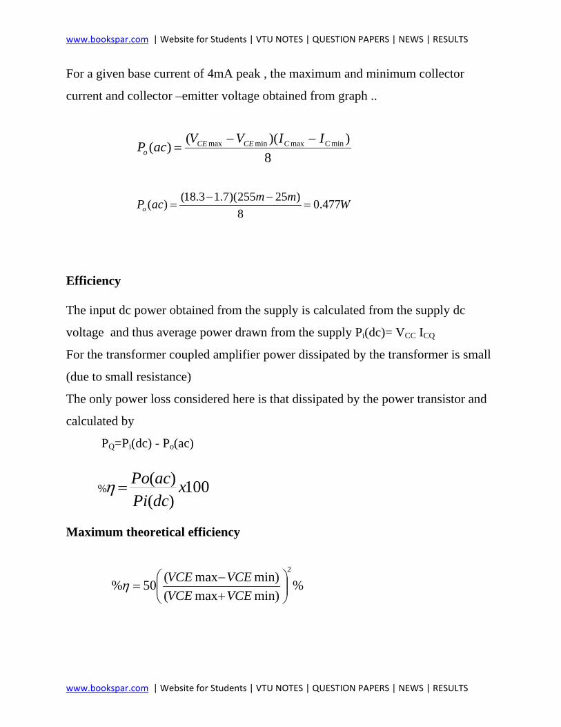
For a given base current of 4mA peak , the maximum and minimum collector
current and collector –emitter voltage obtained from graph ..
Efficiency The input dc power obtained from the supply is calculated from the supply dc
voltage and thus average power drawn from the supply Pi(dc)= VCC ICQ
For the transformer coupled amplifier power dissipated by the transformer is small
(due to small resistance)
The only power loss considered here is that dissipated by the power transistor and
calculated by
PQ=Pi(dc) - Po(ac)
Maximum theoretical efficiency
8))(()( minmaxminmax CCCECE
oIIVVacP −−
=
WmmacPo 477.08
)25255)(7.13.18()( =−−
=
100)()(
% xdcPiacPo=η
%min)max(min)max(50%
2
+−
=VCEVCEVCEVCEη
www.bookspar.com | Website for Students | VTU NOTES | QUESTION PAPERS | NEWS | RESULTS
www.bookspar.com | Website for Students | VTU NOTES | QUESTION PAPERS | NEWS | RESULTS
Larger the value of VCEmax and smaller the value of VCEmin, the closer the
efficiency approaches the theoretical limit of 50%
Numerical
Calculate the efficiency of a transformer coupled class A amplifier for a supply of
12V and outputs of :
a. V(p)=12V
b. V(p)=6V
c. V(p)=2V
Solution :
Here VCE=VCC=12V, the maximum and minimum of the voltage swing are
VCEmax=VCEQ+V(p)=12V+12V=24V
VCEmin=VCEQ-V(p)=12V-12V=0V
This results in efficiency of ,
Case ii.
VCEmax=VCEQ+V(p)=12V+6V=18V
VCEmin=VCEQ-V(p)=12V-6V=6V
This results in efficiency of 12.5%
Case iii.
VCEmax=VCEQ+V(p)=12V+2V=14V
VCEmin=VCEQ-V(p)=12V-2V=10V
This results in efficiency of 1.39%
%5002402450%
2
=
+−
=η
www.bookspar.com | Website for Students | VTU NOTES | QUESTION PAPERS | NEWS | RESULTS
www.bookspar.com | Website for Students | VTU NOTES | QUESTION PAPERS | NEWS | RESULTS
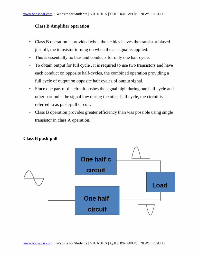
Class B Amplifier operation
• Class B operation is provided when the dc bias leaves the transistor biased
just off, the transistor turning on when the ac signal is applied.
• This is essentially no bias and conducts for only one half cycle.
• To obtain output for full cycle , it is required to use two transistors and have
each conduct on opposite half-cycles, the combined operation providing a
full cycle of output on opposite half cycles of output signal.
• Since one part of the circuit pushes the signal high during one half cycle and
other part pulls the signal low during the other half cycle, the circuit is
referred to as push-pull circuit.
• Class B operation provides greater efficiency than was possible using single
transistor in class A operation.
Class B push-pull
www.bookspar.com | Website for Students | VTU NOTES | QUESTION PAPERS | NEWS | RESULTS
www.bookspar.com | Website for Students | VTU NOTES | QUESTION PAPERS | NEWS | RESULTS
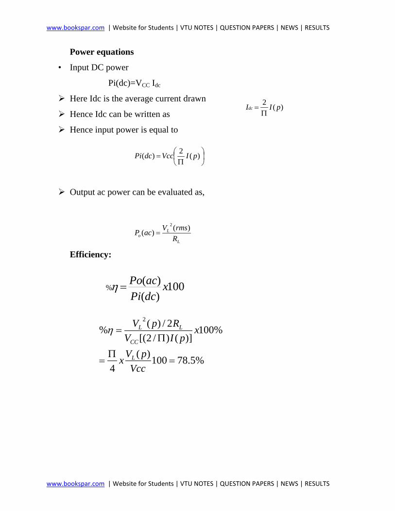
Power equations
• Input DC power
Pi(dc)=VCC Idc
Here Idc is the average current drawn
Hence Idc can be written as
Hence input power is equal to
Output ac power can be evaluated as,
Efficiency:
)(2 pIIdcΠ
=
Π
= )(2)( pIVccdcPi
L
Lo R
rmsVacP )()(2
=
100)()(
% xdcPiacPo=η
%5.78100)(4
%100)]()/2[(
2/)(%2
=Π
=
Π=
VccpVx
xpIV
RpV
L
CC
LLη

www.bookspar.com | Website for Students | VTU NOTES | QUESTION PAPERS | NEWS | RESULTS
www.bookspar.com | Website for Students | VTU NOTES | QUESTION PAPERS | NEWS | RESULTS
Power dissipated by output transistors
• P2Q=Pi(dc)-Po(ac)
• Power handled by each transistor =P2Q/2
Numerical:
For a class B amplifier providing a 20V peak signal to a load of 16 ohms (speaker)
and power supply of VCC=30V, determine the input power, output power, and
circuit efficiency.
Solution:
Hint : use the above derived formulae
• Pi(dc)=23.9W
• Po(ac)=12.5W
• Efficiency=52.3%
For a class B amplifier using supply of VCC=30V and driving a load of 16ohms
determine the maximum input power, output power and transistor dissipation.
Solution:
Hint : use the above derived formulae
• Po(ac)=28.125W
• Pi(dc)=35.81W
• Efficiency=78.54%
• Pq=5.7W
www.bookspar.com | Website for Students | VTU NOTES | QUESTION PAPERS | NEWS | RESULTS
www.bookspar.com | Website for Students | VTU NOTES | QUESTION PAPERS | NEWS | RESULTS
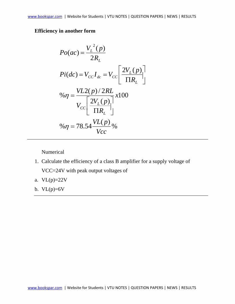
Efficiency in another form
Numerical
1. Calculate the efficiency of a class B amplifier for a supply voltage of
VCC=24V with peak output voltages of
a. VL(p)=22V
b. VL(p)=6V
%)(54.78%
100)(2
2/)(2%
)(2)(
2)()(
2
VccpVL
x
RpVV
RLpVLR
pVVIVdcPi
RpVacPo
L
LCC
L
LCCdcCC
L
L
=
Π
=
Π
==
=
η
η
www.bookspar.com | Website for Students | VTU NOTES | QUESTION PAPERS | NEWS | RESULTS
www.bookspar.com | Website for Students | VTU NOTES | QUESTION PAPERS | NEWS | RESULTS
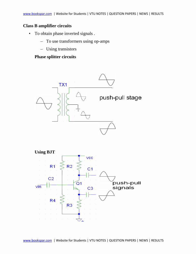
Class B amplifier circuits
• To obtain phase inverted signals .
– To use transformers using op-amps
– Using transistors
Phase splitter circuits
Using BJT
www.bookspar.com | Website for Students | VTU NOTES | QUESTION PAPERS | NEWS | RESULTS
www.bookspar.com | Website for Students | VTU NOTES | QUESTION PAPERS | NEWS | RESULTS
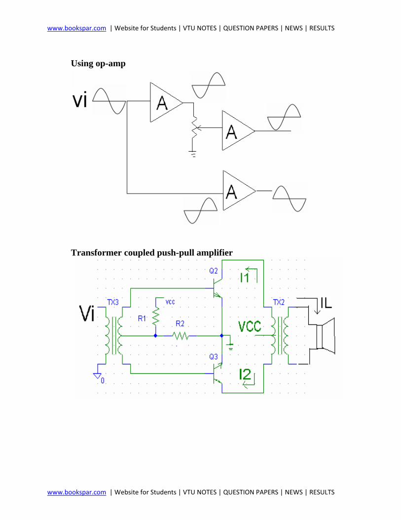
Using op-amp
Transformer coupled push-pull amplifier
www.bookspar.com | Website for Students | VTU NOTES | QUESTION PAPERS | NEWS | RESULTS
www.bookspar.com | Website for Students | VTU NOTES | QUESTION PAPERS | NEWS | RESULTS
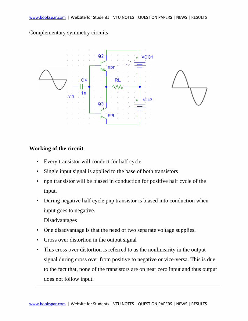
Complementary symmetry circuits
Working of the circuit
• Every transistor will conduct for half cycle
• Single input signal is applied to the base of both transistors
• npn transistor will be biased in conduction for positive half cycle of the
input.
• During negative half cycle pnp transistor is biased into conduction when
input goes to negative.
Disadvantages
• One disadvantage is that the need of two separate voltage supplies.
• Cross over distortion in the output signal
• This cross over distortion is referred to as the nonlinearity in the output
signal during cross over from positive to negative or vice-versa. This is due
to the fact that, none of the transistors are on near zero input and thus output
does not follow input.
www.bookspar.com | Website for Students | VTU NOTES | QUESTION PAPERS | NEWS | RESULTS
www.bookspar.com | Website for Students | VTU NOTES | QUESTION PAPERS | NEWS | RESULTS
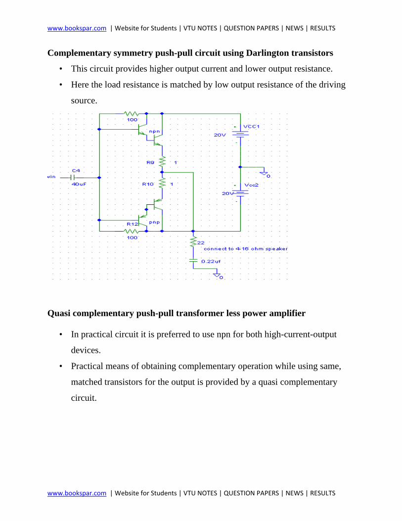
Complementary symmetry push-pull circuit using Darlington transistors
• This circuit provides higher output current and lower output resistance.
• Here the load resistance is matched by low output resistance of the driving
source.
Quasi complementary push-pull transformer less power amplifier
• In practical circuit it is preferred to use npn for both high-current-output
devices.
• Practical means of obtaining complementary operation while using same,
matched transistors for the output is provided by a quasi complementary
circuit.
www.bookspar.com | Website for Students | VTU NOTES | QUESTION PAPERS | NEWS | RESULTS
www.bookspar.com | Website for Students | VTU NOTES | QUESTION PAPERS | NEWS | RESULTS
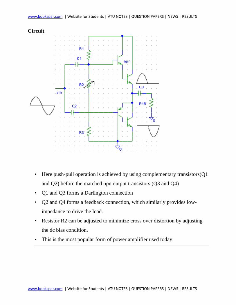
Circuit
• Here push-pull operation is achieved by using complementary transistors(Q1
and Q2) before the matched npn output transistors (Q3 and Q4)
• Q1 and Q3 forms a Darlington connection
• Q2 and Q4 forms a feedback connection, which similarly provides low-
impedance to drive the load.
• Resistor R2 can be adjusted to minimize cross over distortion by adjusting
the dc bias condition.
• This is the most popular form of power amplifier used today.
www.bookspar.com | Website for Students | VTU NOTES | QUESTION PAPERS | NEWS | RESULTS
www.bookspar.com | Website for Students | VTU NOTES | QUESTION PAPERS | NEWS | RESULTS
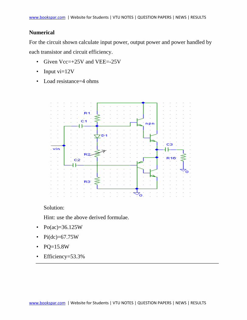
Numerical
For the circuit shown calculate input power, output power and power handled by
each transistor and circuit efficiency.
• Given Vcc=+25V and VEE=-25V
• Input vi=12V
• Load resistance=4 ohms
Solution:
Hint: use the above derived formulae.
• Po(ac)=36.125W
• Pi(dc)=67.75W
• PQ=15.8W
• Efficiency=53.3%

www.bookspar.com | Website for Students | VTU NOTES | QUESTION PAPERS | NEWS | RESULTS
www.bookspar.com | Website for Students | VTU NOTES | QUESTION PAPERS | NEWS | RESULTS
Numerical
For the circuit calculate maximum input power, maximum output power, input
voltage for maximum power operation and power dissipated by the output
transistor at this voltage.
Solution:
Hint: use the above derived formulae
• Pi(dc)=99.47W
• Po(ac)=78.125W
• Efficiency=78.54%
• To achieve maximum power operation the output voltage must be
VL(p)=VCC
• PQ=21.3W
Numerical
For the circuit shown, determine the maximum power dissipated by the output
transistors and the input voltage at which this occurs.
Solution:
• PQ=31.66W
• VL=15.9V

www.bookspar.com | Website for Students | VTU NOTES | QUESTION PAPERS | NEWS | RESULTS
www.bookspar.com | Website for Students | VTU NOTES | QUESTION PAPERS | NEWS | RESULTS
Amplifier distortion • Any signal varying over less than the full 3600 cycle is considered to have
distortion.
• An ideal amplifier is capable of amplifying a pure sinusoidal signal to
provide a larger version, the resulting waveform being a pure sinusoidal
frequency sinusoidal signal.
• When distortion occurs, output will not be an exact duplicate of input signal
(except for magnitude)
• Distortion can occur because the device characteristic is not linear. In this
case non linear or amplitude distortion occurs.
• Distortion can also occur because the circuit elements and devices respond
to the input signal differently at various frequencies, this being frequency
distortion.
• One technique for describing distorted but period waveforms uses Fourier
analysis, a method that describes any periodic waveform in terms of its
fundamental frequency component and frequency components at integer
multiples- these components are called harmonic components or
harmonics.
Example
A fundamental frequency of 1KHz could result in harmonics of 2KHz,3KHz,4KHz
so on.,
• 1KHz is termed as fundamental frequency
• 2KHz is termed as second harmonic
• 3KHz is termed as third harmonic and so on.,
www.bookspar.com | Website for Students | VTU NOTES | QUESTION PAPERS | NEWS | RESULTS
www.bookspar.com | Website for Students | VTU NOTES | QUESTION PAPERS | NEWS | RESULTS
Harmonic Distortion • A signal is considered to have harmonic distortion when there are harmonic
frequency components.
• If fundamental frequency has amplitude A1, and nth frequency component
has an amplitude of An.
• Harmonic distortion can be defined as
% nth harmonic distortion=
Numerical
Calculate the harmonic distortion components for an output signal having
fundamental amplitude of 2.5V, second harmonic amplitude of 0.1V, and fourth
harmonic amplitude of 0.05V.
Solution:
%1001
% xAAn
D =
%2%1005.2
05.0%10014
%
%4%1005.21.0%100
13
%
%10%1005.2
25.0%10012
%
===
===
===
xxAA
D
xxAA
D
xxAA
D
www.bookspar.com | Website for Students | VTU NOTES | QUESTION PAPERS | NEWS | RESULTS
www.bookspar.com | Website for Students | VTU NOTES | QUESTION PAPERS | NEWS | RESULTS
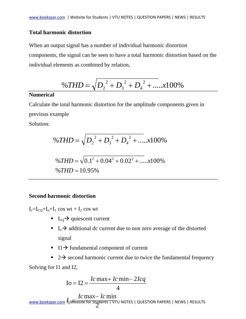
Total harmonic distortion When an output signal has a number of individual harmonic distortion
components, the signal can be seen to have a total harmonic distortion based on the
individual elements as combined by relation,
Numerical
Calculate the total harmonic distortion for the amplitude components given in
previous example
Solution:
Second harmonic distortion Ic=ICQ+Io+I1 cos wt + I2 cos wt
IcQ quiescent current
Io additional dc current due to non zero average of the distorted
signal
I1 fundamental component of current
2 second harmonic current due to twice the fundamental frequency
Solving for I1 and I2,
%100.....% 24
23
22 xDDDTHD +++=
%95.10%%100.....02.004.01.0% 222
=+++=
THDxTHD
%100.....% 24
23
22 xDDDTHD +++=
2minmax
42minmaxI2Io
1IcIcI
IcqIcIc
−=
−+==
www.bookspar.com | Website for Students | VTU NOTES | QUESTION PAPERS | NEWS | RESULTS
www.bookspar.com | Website for Students | VTU NOTES | QUESTION PAPERS | NEWS | RESULTS
Definition of second harmonic can be
In voltage terms
Numerical An output waveform displayed on oscilloscope provides the following
measurements,
i.VCEmin=1V; VCEmax=22V;VCEQ=12V
ii.VCEmin=4V;VCEmax=20V;VCEQ=12V
solution:
( )%1002
1
2minmax
minmaxx
VV
VVVD
CECE
CEQCECE
−
−+=
%100)(
21
2 xVV
VVVD
CEMINCEMAX
CEQCEMINCEMAX
−
−+=
( )
( ))%(0%100
422
1242021
2..
%38.2%100122
1212221
2..
distotionnoxDi
xDi
−=−
−+=
=−
−+=

www.bookspar.com | Website for Students | VTU NOTES | QUESTION PAPERS | NEWS | RESULTS
www.bookspar.com | Website for Students | VTU NOTES | QUESTION PAPERS | NEWS | RESULTS
Power of signal having distortion
• Power delivered to the load resistor Rc due to the fundamental component of the distorted signal is
• Total power due to all the harmonic components of the distorted signal is, In terms of Total harmonic distortion
Numerical For harmonic distortion reading of D2=0.1,D3=0.02 and D4=0.01, with I1=4A and
Rc=8 ohms, calculate THD, fundamental power component and total power.
Solution: THD=0.1
P1=64W
P=64.64W
Graphical description of harmonic components of distorted signal
• All the components are obtained by Fourier analysis
• Conclusion: any periodic signal can be represented by adding a fundamental
component and all harmonic components varying in amplitude and at
various phase angles.
21
21 cRIP =
2......)( 2
32
22
1RcIIIP +++=
12
21
23
22
)1(2
......)1(
PTHDP
RcIDDP
+=
+++=

www.bookspar.com | Website for Students | VTU NOTES | QUESTION PAPERS | NEWS | RESULTS
www.bookspar.com | Website for Students | VTU NOTES | QUESTION PAPERS | NEWS | RESULTS
Power transistor heat sinking
Heat is produced in transistors due to the current flowing through them. If you find
that a transistor is becoming too hot to touch it certainly needs a heat sink! The
heat sink helps to dissipate (remove) the heat by transferring it to the surrounding
air.
Heat sink
• Maximum power handled by a particular device and the temperature of the
transistor junction are related since the power dissipated causes an increase
in temperature at the junction of the device.
• Example : a 100 W transistor will provide more power than 10 W transistor.
• Proper heat sinking techniques will allow operation of a device at about one-
half its maximum power rating.
• There are two types of bipolar transistors
Germanium
Junction temperature : 100 – 1100C
Silicon
Junction temperature : 150 – 2000C
• Silicon transistors provide greater maximum temperature
• Average power dissipated may be approximated by
PD=VCEIC
• This power dissipation is allowed only up to a maximum temperature.
www.bookspar.com | Website for Students | VTU NOTES | QUESTION PAPERS | NEWS | RESULTS
www.bookspar.com | Website for Students | VTU NOTES | QUESTION PAPERS | NEWS | RESULTS
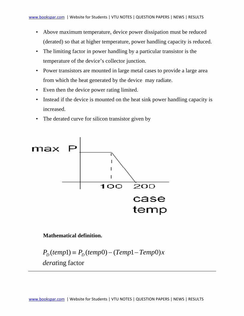
• Above maximum temperature, device power dissipation must be reduced
(derated) so that at higher temperature, power handling capacity is reduced.
• The limiting factor in power handling by a particular transistor is the
temperature of the device’s collector junction.
• Power transistors are mounted in large metal cases to provide a large area
from which the heat generated by the device may radiate.
• Even then the device power rating limited.
• Instead if the device is mounted on the heat sink power handling capacity is
increased.
• The derated curve for silicon transistor given by
Mathematical definition.
factor ing)01()0()1(
deratxTempTemptempPtempP DD −−≡
www.bookspar.com | Website for Students | VTU NOTES | QUESTION PAPERS | NEWS | RESULTS
www.bookspar.com | Website for Students | VTU NOTES | QUESTION PAPERS | NEWS | RESULTS
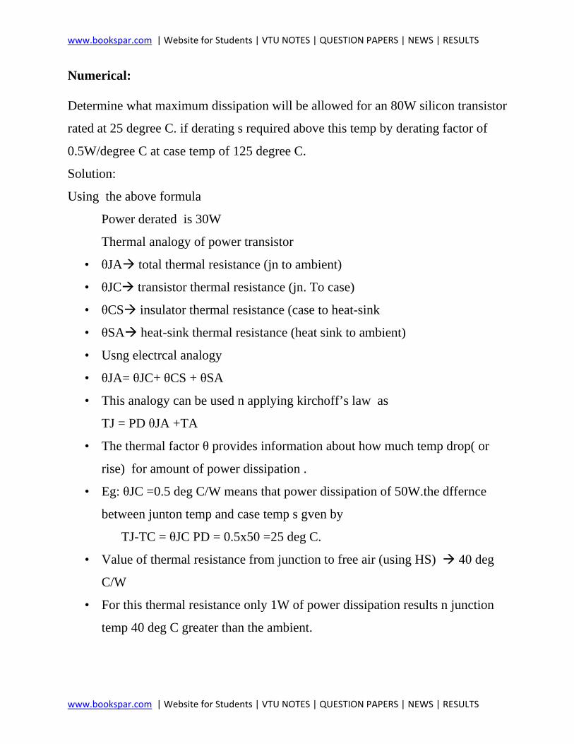
Numerical: Determine what maximum dissipation will be allowed for an 80W silicon transistor
rated at 25 degree C. if derating s required above this temp by derating factor of
0.5W/degree C at case temp of 125 degree C.
Solution:
Using the above formula
Power derated is 30W
Thermal analogy of power transistor
• θJA total thermal resistance (jn to ambient)
• θJC transistor thermal resistance (jn. To case)
• θCS insulator thermal resistance (case to heat-sink
• θSA heat-sink thermal resistance (heat sink to ambient)
• Usng electrcal analogy
• θJA= θJC+ θCS + θSA
• This analogy can be used n applying kirchoff’s law as
TJ = PD θJA +TA
• The thermal factor θ provides information about how much temp drop( or
rise) for amount of power dissipation .
• Eg: θJC =0.5 deg C/W means that power dissipation of 50W.the dffernce
between junton temp and case temp s gven by
TJ-TC = θJC PD = 0.5x50 =25 deg C.
• Value of thermal resistance from junction to free air (using HS) 40 deg
C/W
• For this thermal resistance only 1W of power dissipation results n junction
temp 40 deg C greater than the ambient.
www.bookspar.com | Website for Students | VTU NOTES | QUESTION PAPERS | NEWS | RESULTS
www.bookspar.com | Website for Students | VTU NOTES | QUESTION PAPERS | NEWS | RESULTS
• A HS can now be seen to provide a low thermal resistance between case and
air much less than 40 deg C/W value of case alone. Using HS having
• θSA 2 deg C/W
And insulating thermal resistance (case to HS)
• θCS 0. 8 deg C/W
• Finally for transistor
• θJC 0.5 deg C/W
• θJA= θJC+ θCS + θSA
= 2.0 +0.8 +0.5
= 3.3 deg C/W
With HS thermal resistance between air and the junction is only 3.3 deg C/W
compared 40 deg C/W for transistor operating directly in to free air
Numerical:
A silicon power transistor s operated with a HS θSA = 1.5 deg C/w. the transistor
rated at 150W(25 deg C) has θJC =0.5 deg C/W and the mounting insulation has
θCS =0.6 deg C /W. what s the max power dissipated f the ambient temp s 40 deg
C and TJ max s 200 deg C
• Solution : pd =(TJ-TA)/ θSA + θJC + θCS
= 61.5W
www.bookspar.com | Website for Students | VTU NOTES | QUESTION PAPERS | NEWS | RESULTS
www.bookspar.com | Website for Students | VTU NOTES | QUESTION PAPERS | NEWS | RESULTS
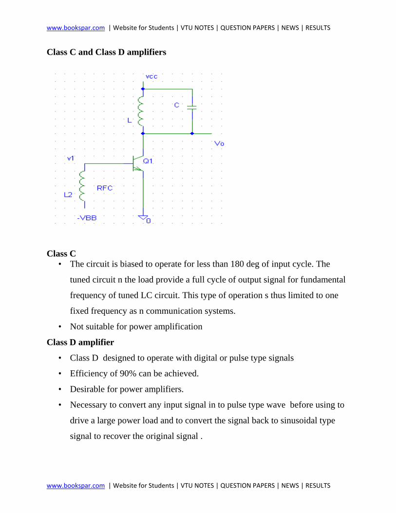
Class C and Class D amplifiers
Class C
• The circuit is biased to operate for less than 180 deg of input cycle. The
tuned circuit n the load provide a full cycle of output signal for fundamental
frequency of tuned LC circuit. This type of operation s thus limited to one
fixed frequency as n communication systems.
• Not suitable for power amplification
Class D amplifier
• Class D designed to operate with digital or pulse type signals
• Efficiency of 90% can be achieved.
• Desirable for power amplifiers.
• Necessary to convert any input signal in to pulse type wave before using to
drive a large power load and to convert the signal back to sinusoidal type
signal to recover the original signal .
www.bookspar.com | Website for Students | VTU NOTES | QUESTION PAPERS | NEWS | RESULTS
www.bookspar.com | Website for Students | VTU NOTES | QUESTION PAPERS | NEWS | RESULTS
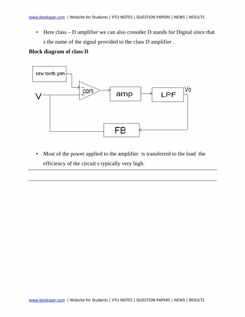
• Here class – D amplifier we can also consider D stands for Digital since that
s the name of the signal provided to the class D amplifier .
Block diagram of class D
• Most of the power applied to the amplifier is transferred to the load the
efficiency of the circuit s typically very high.