Embed Size (px)
Citation preview
June 29, 2004
Poly-SiGe MEMS for Modular Post-CMOS Integrated Microsystems
Roger T. Howe1,2,3 and Tsu-Jae King1
Depts. of 1EECS and 2ME3Berkeley Sensor & Actuator Center
University of California at Berkeley
June 29, 2004
Outline
• Introduction– Motivation for modular integration– Alternative integration approaches
• Poly-SiGe as a MEMS material system– Basic material properties– Process integration– Demonstration platform: RF MEMS
• Conclusion

June 29, 2004
Example: MEMS GyroscopeA. Seshia et al., IEEE MEMS 2002 (Las Vegas, Nevada)
Resonant mass: 700 µm x 700 µm x 2 µm,suspended 2 µm above substrate
Structural material: poly-SiBSAC design;
Sandia iMEMS process
Why not build the gyroscope on top of CMOS?
700 µm

June 29, 2004
CMOS/MEMS 1.02 MHz Oscillator• Pierce sustaining amplifier co-fabricated in
Sandia 2 µm CMOS-last iMEMS process
Trey A. Roessig, R. T. Howe, A. P. Pisano, and J. H. Smith,Solid-State Sensor and Actuator Workshop, Hilton Head, S.C., 1998.
DETF resonatorwith driveand senseelectrodes
200 µm
300 nm-thick poly-Si interconnect: low-pass filter!

June 29, 2004
Why Modular Integration?Allows for separate development and optimization of electronics & MEMS processes
• MEMS first:Electronics and MEMS cannot be stackedIC foundries are wary of pre-processed wafers
• MEMS last:Chip area can be minimizedIC foundry can be used, if MEMS thermal budget is low
June 29, 2004
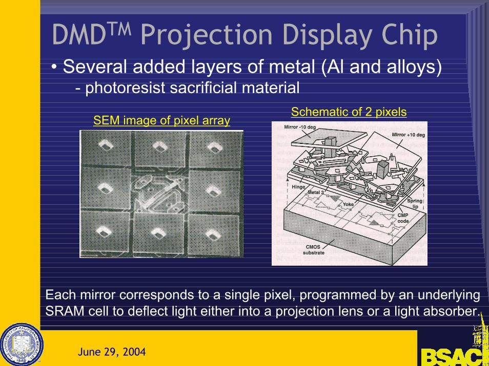
DMDTM Projection Display Chip• Several added layers of metal (Al and alloys)
- photoresist sacrificial materialSchematic of 2 pixels
SEM image of pixel array
Each mirror corresponds to a single pixel, programmed by an underlying SRAM cell to deflect light either into a projection lens or a light absorber.
June 29, 2004
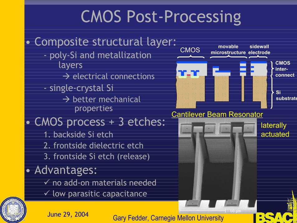
CMOS Post-Processing
Gary Fedder, Carnegie Mellon University
CMOS sidewalltrode
• Composite structural layer:- poly-Si and metallization
layerselectrical connections
- single-crystal Sibetter mechanical properties
• CMOS process + 3 etches:1. backside Si etch2. frontside dielectric etch3. frontside Si etch (release)
• Advantages:no add-on materials neededlow parasitic capacitance
Cantilever Beam Resonatorlaterallyactuated
movablemicrostructure elec
CMOSinter-connect
Si substrate

June 29, 2004
MEMS in the Metallization StackJ. L. Lund et al., 2002 Solid-State Sensor, Actuator and Microsystems Workshop
Composite structural layer:- thin metal layer electrical connection- thick dielectric layer good mechanical
properties
Can stack MEMS directly on top of (Bi-)CMOSlow parasitic resistance and capacitance, small chip size
Fixed beam resonator (vertically actuated)

June 29, 2004
The Ideal MEMS Technology
For low cost and high performance, we want:
• Low thermal process budgetcan use semiconductor foundry for electronics
• Capabilities similar to poly-Si MEMScan leverage MEMS foundry processes can leverage MEMS industry design experience

June 29, 2004
Outline
• Introduction– Motivation for modular integration– Alternative integration approaches
• Poly-SiGe as a MEMS material system– Basic material properties– Process integration– Demonstration platform: RF MEMS
• Conclusion
June 29, 2004
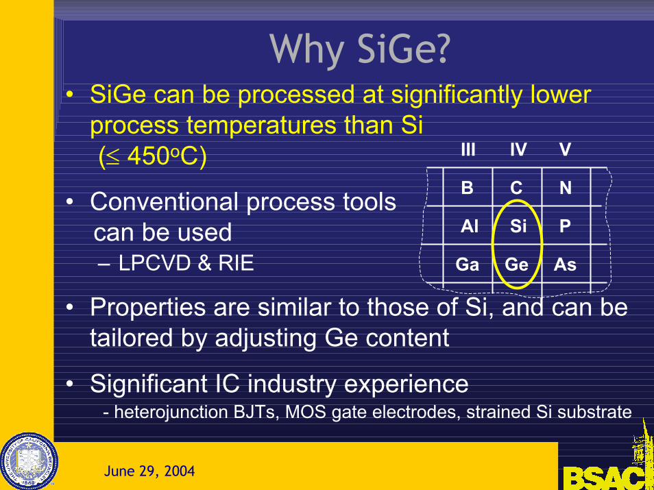
Why SiGe?• SiGe can be processed at significantly lower
process temperatures than Si(≤ 450oC)
• Conventional process toolscan be used– LPCVD & RIE
• Properties are similar to those of Si, and can be tailored by adjusting Ge content
• Significant IC industry experience- heterojunction BJTs, MOS gate electrodes, strained Si substrate
CB
IV
N
SiAl
VIII
P
Ga Ge As
June 29, 2004
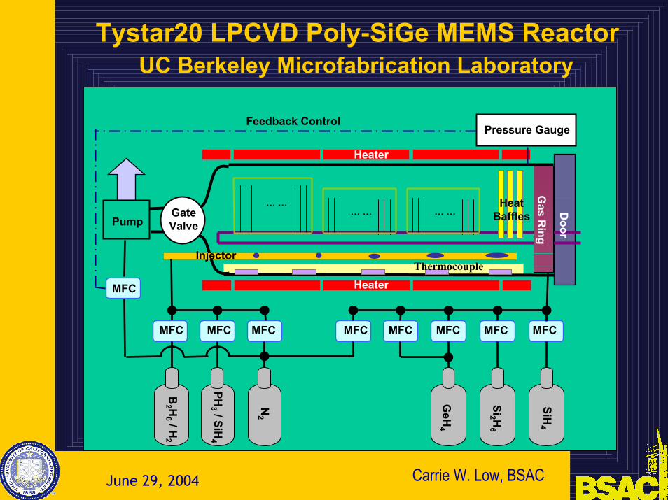
Tystar20 LPCVD Poly-SiGe MEMS ReactorUC Berkeley Microfabrication Laboratory
Heater
… …… …
Gas R
ing
Injector
Heat BafflesGate
Valve
MFC
Pump
Thermocouple
MFC MFC MFC MFC MFC MFC MFC MFC
N2
Si2 H6
SiH4
GeH
4
Heater
Door
B2 H
6 / H2
PH3 / SiH
4
Pressure GaugeFeedback Control
… …
Carrie W. Low, BSAC

June 29, 2004
Ge as a Sacrificial Material • Ge-rich films etch rapidly in oxidizing solutions
non-HF-based etchant (heated H2O2)eliminates need for protective layer for
electronics
high etch selectivity to poly-Si, SiO2, Si3N4, metals
Etch Rates (µm/min)
*J. M. Heck et al., Tranducers’ 99
HF RCA, SC1 H2O2 Cl2/HBr PlasmaPoly-Ge ~0 3.0 0.4 0.41Poly-Si0.2Ge0.8 ~0 0.75 0.08 0.37Poly-Si0.4Ge0.6 ~0 0.06 ~0 0.31Poly-Si ~0 ~0 ~0 0.16Annealed PSG 3.6 ~0 ~0 ~0
*
June 29, 2004
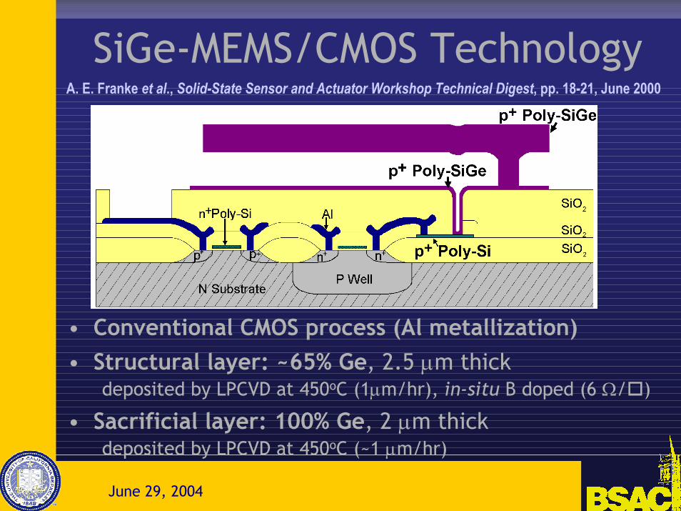
SiGe-MEMS/CMOS TechnologyA. E. Franke et al., Solid-State Sensor and Actuator Workshop Technical Digest, pp. 18-21, June 2000
• Conventional CMOS process (Al metallization)• Structural layer: ~65% Ge, 2.5 µm thick
deposited by LPCVD at 450oC (1µm/hr), in-situ B doped (6 Ω/ )
• Sacrificial layer: 100% Ge, 2 µm thickdeposited by LPCVD at 450oC (~1 µm/hr)

June 29, 2004
Integrated SiGe-MEMS/CMOS
Resonator next to Amplifier• conventional layout
Resonator on top of Amplifiersmaller area --> lower costreduced interconnect parasitics --> improved performance
A. E. Franke et al., IEEE J. MEMS, 12, 160 (2003).

June 29, 2004
Si0.35Ge0.65 Resonator Response
19580 19585 19590 19595 19600 19605 19610 19615 19620
-140
-120
-100
-80
-60
-40
-2019.6kHz comb-drive: Q ~ 31,100
T/R
(dB)
Frequency (Hz)
S. A. Bhave et al., Solid-State Sensor and Actuator Workshop Technical Digest, pp. 34-37, 2002

June 29, 2004
Properties of P+ poly-Si0.35Ge0.65as deposited at 450oC
• E = 155 ± 5 GPa• Stress = -10 MPa (compressive)• Stress gradient ≅ 10-4/µm for a 2-µm-
thick film- 100 µm cantilever beam bends up 0.7 µm at
the tip• Fracture strain = 1.2 ± 0.1%
- comparable to poly-Si• Q = 31,000 at 20 kHz in vacuum
June 29, 2004
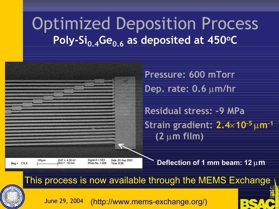
Optimized Deposition ProcessPoly-Si0.4Ge0.6 as deposited at 450oC
Pressure: 600 mTorrDep. rate: 0.6 µm/hr
Residual stress: -9 MPaStrain gradient: 2.4×10⁻⁵ µm-1
(2 µm film)
Deflection of 1 mm beam: 12 µm
This process is now available through the MEMS Exchange
(http://www.mems-exchange.org/)
June 29, 2004
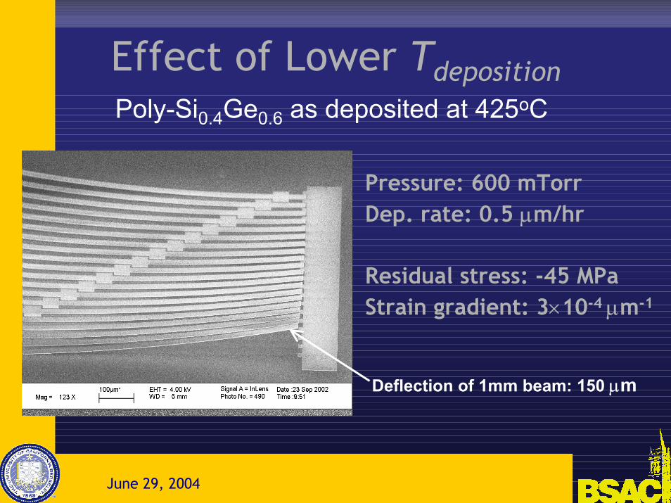
Effect of Lower TdepositionPoly-Si0.4Ge0.6 as deposited at 425oC
Pressure: 600 mTorrDep. rate: 0.5 µm/hr
Residual stress: -45 MPaStrain gradient: 3×10⁻⁴ µm-1
Deflection of 1mm beam: 150 µm
June 29, 2004
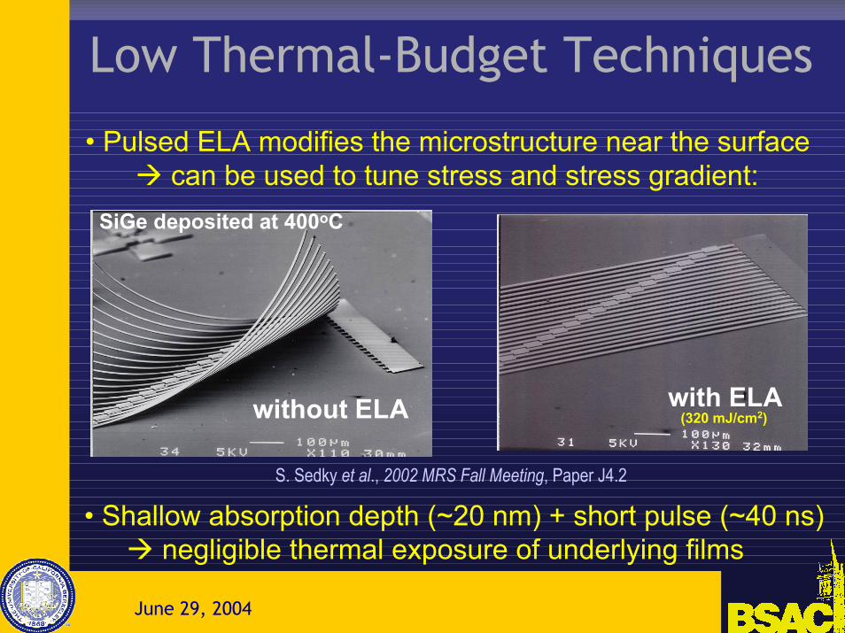
Low Thermal-Budget Techniques
• Pulsed ELA modifies the microstructure near the surface can be used to tune stress and stress gradient:
without ELA with ELA
S. Sedky et al., 2002 MRS Fall Meeting, Paper J4.2
(320 mJ/cm2)
SiGe deposited at 400oCSiGe deposited at 400oC
• Shallow absorption depth (~20 nm) + short pulse (~40 ns)negligible thermal exposure of underlying films

June 29, 2004
Motivating Application:Poly-SiGe Integrated RF MEMS
RESDrive Electrode Sense Electrode
Microshell Encapsulation(anchors not shown)
DC Bias toResonator
Shielded Interconnectto Drive Electrode Shielded
Vertical SignalPath to Gate ofInput Transistor
5-level metalfoundry CMOS
Poly-SiGe RFMEMS technology
R. T. Howe, T.-J. King, and A. P. Pisano, DARPA MTO NMASP Projects.

June 29, 2004
Poly-SiGe Technology for RF Resonators
• Planar bulk-mode acoustic modes• Maximize capacitive transduction efficiency
high aspect ratio nanogaps (50 to 100 nm)
• Spacer technology challenges:• Selectivity of H2O2
sacrificial etch• Step coverage
2 µm
2 µm
(b)
(a)
Poly-SiGe
1 µm
1 µm
Poly-SiGe
Poly-Ge
Poly-SiGe
Poly-SiGe
Poly-SiGe
Poly-SiGe
2 µm
2 µm
(b)
(a)
Poly-SiGe
1 µm
1 µm
Poly-SiGe
Poly-Ge
Poly-SiGe
Poly-SiGe
Poly-SiGe
Poly-SiGe
Brian Bircumshaw et al, IEEE MEMS ‘04
June 29, 2004
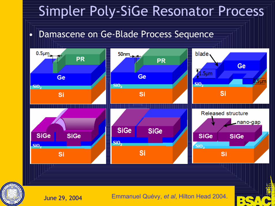
Simpler Poly-SiGe Resonator Process
• Damascene on Ge-Blade Process Sequence
Emmanuel Quévy, et al, Hilton Head 2004.
June 29, 2004
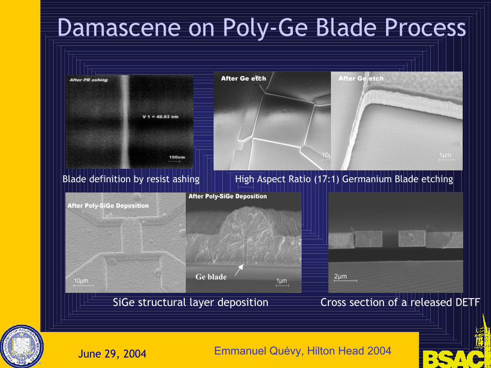
Damascene on Poly-Ge Blade Process
Blade definition by resist ashing High Aspect Ratio (17:1) Germanium Blade etching
Ge blade
SiGe structural layer deposition Cross section of a released DETF
Emmanuel Quévy, Hilton Head 2004

June 29, 2004
VHF Poly-SiGe Resonator MeasurementsBulk Longitudinal Resonator
RF/LO Technique
74 MHz Fundamental Mode 205 MHz Third Harmonic
Emmanuel Quévy, et al, Hilton Head 2004

June 29, 2004
Outline
• Introduction– Motivation for modular integration– Alternative integration approaches
• Poly-SiGe as a MEMS material system– Basic material properties– Process integration– Demonstration platform: RF MEMS
• Conclusion
June 29, 2004
Conclusions• Integration of MEMS with foundry electronics
can lead to enhanced functionality and/or performance
Range of applications will expand in the future
• Different approaches are possibleThe best choice will likely depend on the application
• Low-temperature (<450oC) poly-SiGe can leverage MEMS foundry processes & design infrastructureWork is in progress to demonstrate poly-SiGe RF MEMS
technology with integration on sub-micron CMOS

June 29, 2004
Acknowledgments
• Postdoc: Emmanuel Quévy• Current graduate students: Sunil Bhave,
Brian Bircumshaw,Blake Lin, Carrie Low• Process engineer: Hideki Takeuchi
• DARPA MTO NMASP Program,Dr. Daniel Radack, Program Manager