Embed Size (px)
Citation preview

Pipelined A/D ConverterTop Level System Design
Sack Savengsveksa

Outline
• Introduction• Pipelined A/D
– Architecture– Non-idealities
• System Specification• Error Budget
– Residue Stage/Op-amp– Comparators– Voltage Reference
• Test Modes• Conclusion
Introduction
• Most A/D are Application Driven- Video - DSP Interface
• Behavioral Modeling (Top-Down Approach)- Effective Way to Check System Architecture- Define Block Specification- Cadence(VerilogA), Mentor Graphics, Matlab/Simulink, Excel
• Why 8bit?-Constrained by Die Size
• Why 20MSample/s?-Low/Medium Speed
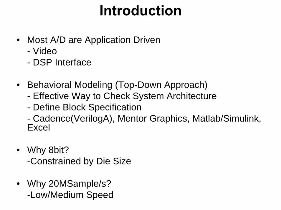
P u b lis h e d P ip e l in e d A D C
0
2 0
4 0
6 0
8 0
1 0 0
1 2 0
1 4 0
1 6 0
1 8 0
2 0 0
2 2 0
6 8 1 0 1 2 1 4 1 6N u m b e r o f B its
Con
vers
ion
Spee
d (M
S/s)
[2 ][1 ]
[1] S.H. Lewis et. al, 3/92[2] A. Abo, P.R. Gray, 5/99

Technology vs. Conversion Speed
0102030405060708090
100110120130140150160170180190200210
0 0.2 0.4 0.6 0.8 1 1.2
Technology(um)

General Architecture
Figure 1[1]
•Trade Latency for speed•Allows For Concurrent Operation

1 bit/stage Architecture+Vref+Vref
-Vref -Vref
+Vref-Vref Vin
Vout=2Vin±Vref
0
Vin > 0, Vout=2Vin-VrefVin < 0, Vout=2Vin+Vref
Vout
•Require Some Type of Calibration/Error Correction Scheme

2bit/stage Architecture
Figure 2[2]
• Interstage Gain=4, requires more power & Bandwidth.
• Susceptible to over-range problems
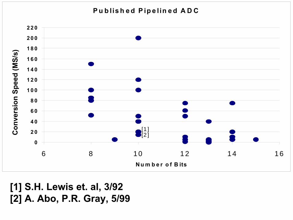
1.5bit/stage Architecture• For an 8 bit Pipelined A/D:
– 6 (1.5bit per stage) + 1 (2bit per stage)– Front End SHA & 1st Stage need to be 8bit accurate.
• Digital Error Correction relaxes sub-ADC requirements.
•Requires a precise Gain of Two for Residue Stage.
•Maximizes the Bandwidth of Residue Stage, BW depends on Interstage Gain.

1.5bps Architecture
Figure 3[2]
•Large Correctable Range: Vref/4Relax Comparator Precision
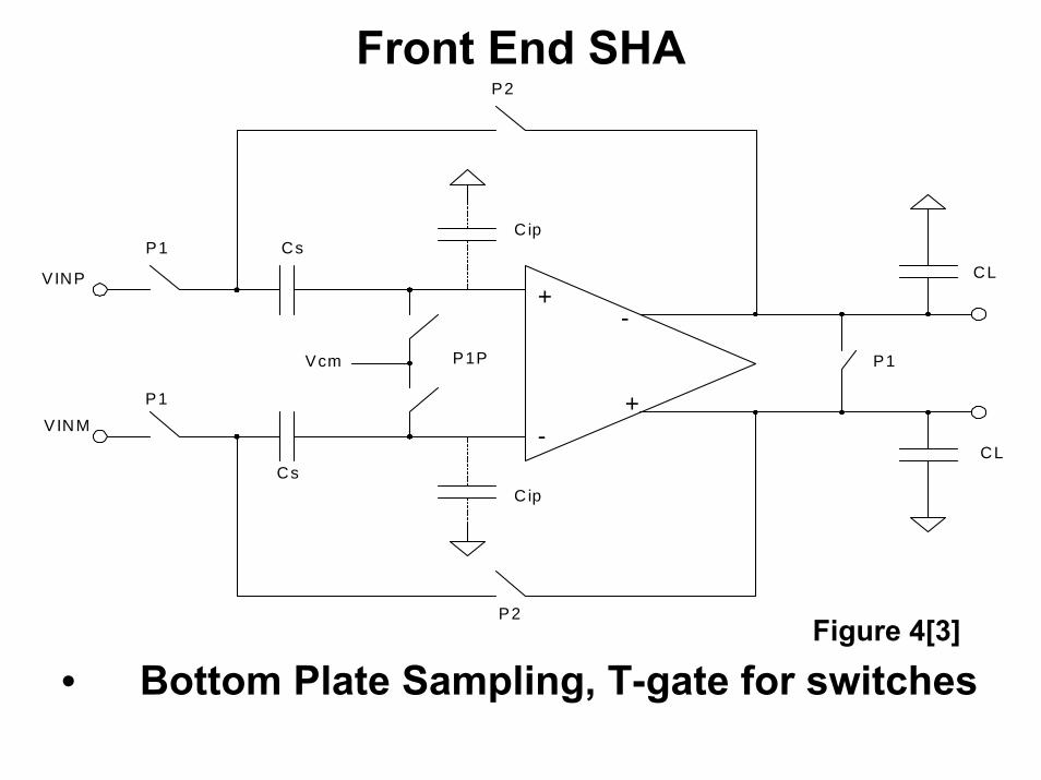
Front End SHA
Cs
Cs
Vcm
P1
P1
P2
P2
P1
CL
CL
P1P
VINP
VINM
+
+
-
-
Cip
C ip
Figure 4[3]
• Bottom Plate Sampling, T-gate for switches

Errors Affecting Accuracy
• Interstage Gain Error- Capacitor Mismatch
Calibration,Trimming- Finite Gain Error
High Gain Opamp- Settling Time
• D/A Non-linearity -1.5bps Architecture, Inherently Linear
• A/D Non-linearity-Digital Error Correction

System Specifications
• Technology: AMI 0.5u CMOS Process-Double Poly, Triple Metal, VDD=5V
• Resolution: 8 bit • Sampling Frequency: 20MHz• DNL < 0.5LSB, INL < 0.5 LSB• Differential Input Range: 2V• Input Common Mode: 2.5V

Differential Full Scale Range+ V R E F = (3 -2 )= 1 V
-V R E F = (2 -3 )= -1 V
+ V R E F /4 = .2 5 V
-V R E F /4 = - .2 5 V
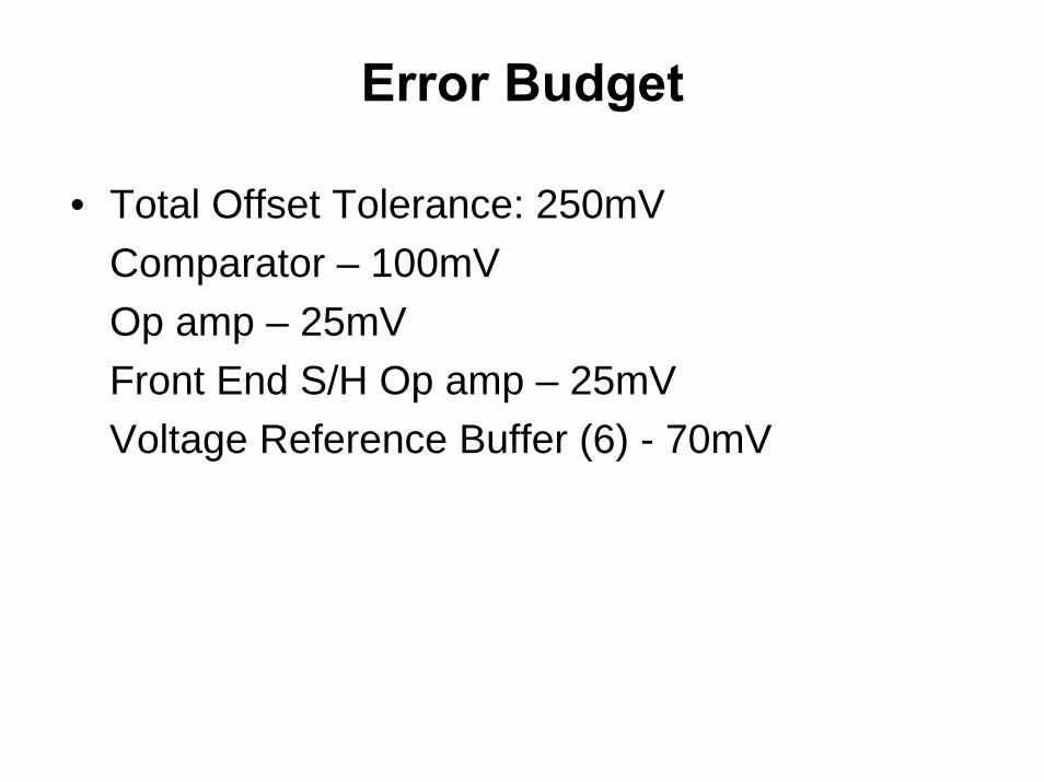
Error Budget
• Total Offset Tolerance: 250mVComparator – 100mVOp amp – 25mVFront End S/H Op amp – 25mVVoltage Reference Buffer (6) - 70mV

Residue Stage/Op Amp
• Error Sources- Capacitor Mismatch- Op amp Finite Gain- Op amp Settling Time
• Capacitor Mismatch- Calibration Techniques- Trimming- Poly/Poly caps have good matching (9-10 bits)

Thermal Noise
Table 1 [2]
• Limits Achievable SNR• For C=500fF => sigma=90uV

SNR
Figure 5[2]
•SNR=6.02*N+1.76dB•SNDR= SNR+Distortion Ratio, SNDR<SNR
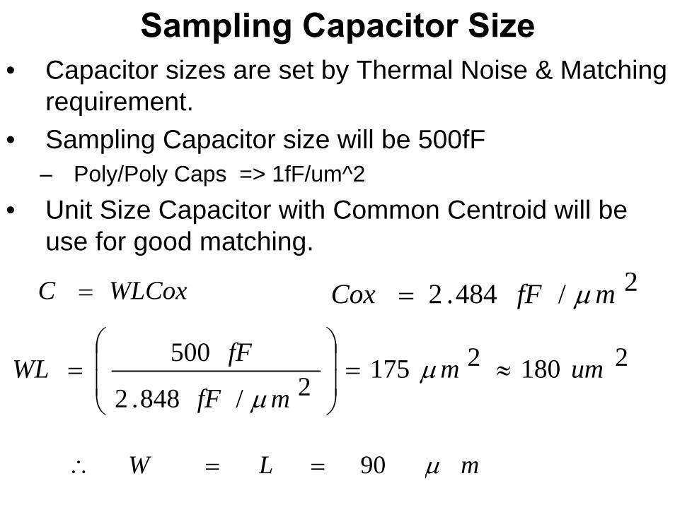
Sampling Capacitor Size• Capacitor sizes are set by Thermal Noise & Matching
requirement.• Sampling Capacitor size will be 500fF
– Poly/Poly Caps => 1fF/um^2 • Unit Size Capacitor with Common Centroid will be
use for good matching.2/484.2 mfFCox µ=WLCoxC =
218021752/848.2
500 ummmfF
fFWL ≈=⎟⎟
⎠
⎞
⎜⎜
⎝
⎛= µ
µ
mLW µ90==∴

Op amp Finite Gain
VrefCfCsVin
CfCsVo ⎟⎟
⎠
⎞⎜⎜⎝
⎛±⎟⎟
⎠
⎞⎜⎜⎝
⎛+= 1
Equation 1[1]
iNiCC
iGG
−<
∆+
∆
2
143
21
VnVrefCC
GGVin
CC
GGVo +⎟
⎠⎞
⎜⎝⎛ ∆
+∆
+±⎟⎠⎞
⎜⎝⎛ ∆
+∆
+≈ 12211'
LSBDNL 5.0< LSBINL 5.0<

=∆GG Finite Gain + Settling Time
βAGG 1
−=∆ 92−=
∆GG
dBdBA 8666 →>∴
&
•Added 20dB for process variations & poorly modeled output impedance.
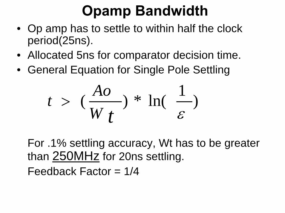
Opamp Bandwidth• Op amp has to settle to within half the clock
period(25ns).• Allocated 5ns for comparator decision time.• General Equation for Single Pole Settling
For .1% settling accuracy, Wt has to be greater than 250MHz for 20ns settling. Feedback Factor = 1/4
)1ln(*)(εtW
Aot >

Opamp Specifications
• Open Loop Gain: 86 dB
• Unity Gain Bandwidth > 250MHz
• Phase Margin: 75 degrees
• Output Swing: 1 V differential
• Offset Voltage: 25mV

Reference Generator
• Total Offset Error (6 Buffer): 70mV• Reference Voltages: 2V differential
-Vrefp: 3.0-Vrefp/4: 2.625-Vcm: 2.5-Vrefn/4: 2.375-Vrefn: 2.0
Comparator• Offset Error: 100mV• Comparator Decision Time: 5ns

Test Modes• Clock Generator
- Adjustable Non overlap Time• Voltage References
-External Bias Current-External Resistor for Reference Control
• Residue Stage-Adjustable Bias Current
• Comparator-Adjustable Bias Current
• Digital Decode Logic-External Decoder
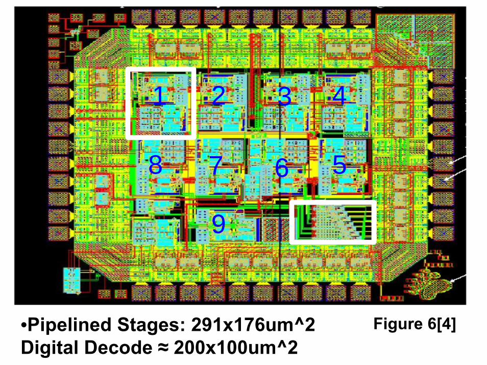
•Pipelined Stages: 291x176um^2Digital Decode ≈ 200x100um^2
2
5
3 4
9
678
1
Figure 6[4]

Conclusions
• 1.5bps Pipelined Architecture is Chosen• Error Tolerances
– Behavioral Models to refine block specifications.• Test Modes
– Work in progress.• Top Level Simulation
– Start integrating blocks for top level simulation.• Layout
-Big Challenge Ahead

References• [1] A. Abo “Design for reliability of low-voltage, switched
capacitor circuits (thesis),” Ph.D. dissertation, University of California, Berkeley,May1999
• [2] T.Cho, “Low-power, low-voltage analog-to-digital conversion techniques using pipelined architectures, Ph.D. dissertation, University of California, Berkeley, 1995.
• [3] Y. Park et. al, “A 10b 100MSample/s CMOS Pipelined ADC with 1.8V Power Supply,” IEEE ISSCC, vol. XLIV, pp. 130-131, Feb. 2001
• [4] Kannan Socklingham et. al, “10-Bit 5MHz Pipeline A/D Converter,” University of Maine, July 2002
• [5] Johns & Martin, Analog Integrated Circuit Design. New York. John Wiley& Sons, 1997