Embed Size (px)
Citation preview
MT-024TUTORIAL
ADC Architectures V: Pipelined Subranging ADCs
by Walt Kester
INTRODUCTION The pipelined subranging ADC architecture dominates today's applications where sampling rates of greater than 5 MSPS to 10 MSPS are required. Although the flash (all-parallel) architecture (see Tutorial MT-020) dominated the 8-bit video IC ADC market in the 1980s and early 1990s, the pipelined architecture has largely replaced the flash ADC in modern applications. There are a small number of high power Gallium Arsenide (GaAs) flash converters with sampling rates greater than 1 GHz, but resolution is limited to 6 or 8 bits. However, the flash converter still remains a popular building block for higher resolution pipelined ADCs. Applications for pipelined ADCs include video, image processing, communications, and a myriad of others. The architecture lends itself to a variety of relatively low cost IC processes, CMOS and BiCMOS being the most popular. Current technology yields 12- to 16-bit resolution at sampling rates greater than 100 MSPS. BASIC SUBRANGING ADC ARCHITECTURE The pipelined ADC had its origins in the subranging architecture which was first used in the 1950s as a means to reduce the component count and power in tunnel diode and vacuum tube flash ADCs (see References 1, 2). A block diagram of the subranging architecture is shown in Figure 1, where a 6-bit, two-stage ADC is shown.
SAMPLEAND HOLD Σ
+
–
OUTPUT REGISTER
ANALOGINPUT
DATA OUTPUT, N-BITS = N1 + N2 = 3 + 3 = 6
CONTROL
SAMPLINGCLOCK
See: R. Staffin and R. Lohman, "Signal Amplitude Quantizer,"U.S. Patent 2,869,079, Filed December 19, 1956, Issued January 13, 1959
RESIDUESIGNAL
N1 MSBs (3) N2 LSBs (3)
GN1-BIT(3-BIT)SADC
N1-BIT(3-BIT)SDAC
N2-BIT(3-BIT)SADC
Figure 1: A 6-Bit, Two-Stage Subranging ADC
Rev.A, 10/08, WK Page 1 of 14
MT-024
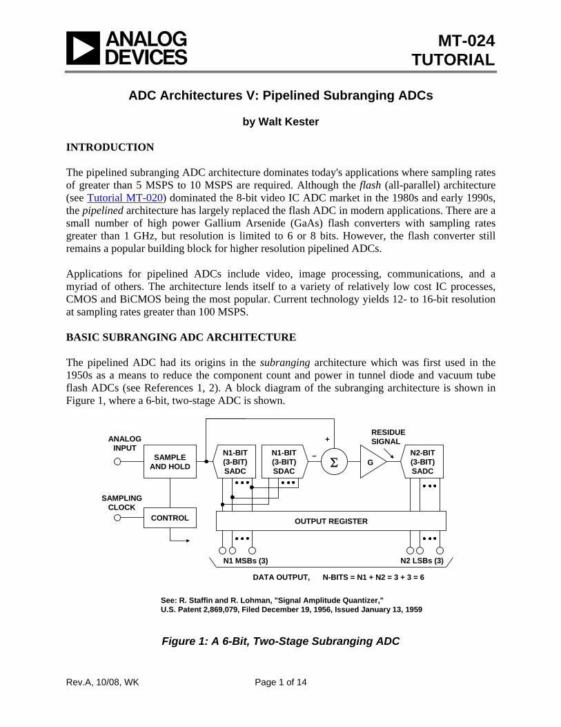
The output of the input sample-and-hold (SHA) is digitized by the first-stage 3-bit sub-ADC (SADC)—a flash converter. The coarse 3-bit MSB conversion is then converted back to an analog signal using a 3-bit sub-DAC (SDAC). The SDAC output is then subtracted from the SHA output, amplified, and applied to a second-stage 3-bit SADC. The "residue signal" is then digitized by the 3-bit second-stage SADC, thereby generating the three LSBs of the total 6-bit output word. This type of ADC is generally referred to as "subranging" because the input range is subdivided into a number of smaller ranges (subranges) which are, in turn, further subdivided. This subranging ADC can best be analyzed by examining the residue waveform at the input to the second-stage ADC as shown in Figure 2. This waveform assumes a low frequency ramp input signal to the overall ADC. In order for there to be no missing codes, the residue waveform must exactly fill the input range of the second-stage ADC, as shown in the ideal case of Figure 2A. This implies that both the N1 SADC and the N1 SDAC must be better than N1 + N2 bits accurate—in the example shown, N1 = 3, N2 = 3, and N1 + N2 = 6. This architecture, as shown, is useful for resolutions up to about 8 bits (N1 = N2 = 4), however maintaining better than 8-bit alignment between the two stages (over temperature variations, in particular) can be difficult. The situation shown in Figure 2B will result in missing codes when the residue waveform goes outside the range of the N2 SADC, "R", and falls within the "X" or "Y" regions—caused by a nonlinear N1 SADC or interstage gain and/or offset mismatch . 0 1 2 3 2N1–12N1–2
MISSING CODES
MISSING CODES
R = RANGEOF N2 SADC
X
R
Y
(A)IDEAL
N1 SADC
(B)NONLINEAR
N1 SADC
0 1 2
3
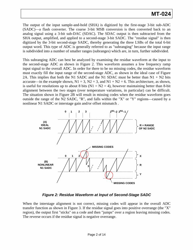
Figure 2: Residue Waveform at Input of Second-Stage SADC When the interstage alignment is not correct, missing codes will appear in the overall ADC transfer function as shown in Figure 3. If the residue signal goes into positive overrange (the "X" region), the output first "sticks" on a code and then "jumps" over a region leaving missing codes. The reverse occurs if the residue signal is negative overrange.
Page 2 of 14
MT-024
ANALOG INPUT
DIGITALOUTPUT
MISSING CODES
MISSING CODES
"STICKS"
"JUMPS"
"JUMPS"
"STICKS"
Figure 3: Missing Codes Due to MSB SADC Nonlinearity or Interstage Misalignment
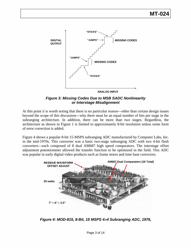
At this point it is worth noting that there is no particular reason—other than certain design issues beyond the scope of this discussion—why there must be an equal number of bits per stage in the subranging architecture. In addition, there can be more than two stages. Regardless, the architecture as shown in Figure 1 is limited to approximately 8-bit resolution unless some form of error correction is added. Figure 4 shows a popular 8-bit 15-MSPS subranging ADC manufactured by Computer Labs, Inc. in the mid-1970s. This converter was a basic two-stage subranging ADC with two 4-bit flash converters—each composed of 8 dual AM687 high speed comparators. The interstage offset adjustment potentiometer allowed the transfer function to be optimized in the field. This ADC was popular in early digital video products such as frame stores and time base correctors.
25 watts
AM687 Dual Comparators (16 Total)RESIDUE WAVEFORMOFFSET ADJUST
7" × 6" × 2.5"
Figure 4: MOD-815, 8-Bit, 15 MSPS 4×4 Subranging ADC, 1976,
Page 3 of 14
MT-024
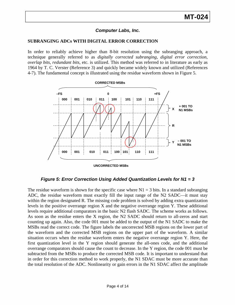
Computer Labs, Inc. SUBRANGING ADCs WITH DIGITAL ERROR CORRECTION In order to reliably achieve higher than 8-bit resolution using the subranging approach, a technique generally referred to as digitally corrected subranging, digital error correction, overlap bits, redundant bits, etc. is utilized. This method was referred to in literature as early as 1964 by T. C. Verster (Reference 3) and quickly became widely known and utilized (References 4-7). The fundamental concept is illustrated using the residue waveform shown in Figure 5.
000 001 010 011 100 101 110 111
R
X
Y
–FS +FS0
CORRECTED MSBs
+ 001 TON1 MSBs
– 001 TON1 MSBs
000 001 010 011 100 101 110 111
UNCORRECTED MSBs
Figure 5: Error Correction Using Added Quantization Levels for N1 = 3 The residue waveform is shown for the specific case where N1 = 3 bits. In a standard subranging ADC, the residue waveform must exactly fill the input range of the N2 SADC—it must stay within the region designated R. The missing code problem is solved by adding extra quantization levels in the positive overrange region X and the negative overrange region Y. These additional levels require additional comparators in the basic N2 flash SADC. The scheme works as follows. As soon as the residue enters the X region, the N2 SADC should return to all-zeros and start counting up again. Also, the code 001 must be added to the output of the N1 SADC to make the MSBs read the correct code. The figure labels the uncorrected MSB regions on the lower part of the waveform and the corrected MSB regions on the upper part of the waveform. A similar situation occurs when the residue waveform enters the negative overrange region Y. Here, the first quantization level in the Y region should generate the all-ones code, and the additional overrange comparators should cause the count to decrease. In the Y region, the code 001 must be subtracted from the MSBs to produce the corrected MSB code. It is important to understand that in order for this correction method to work properly, the N1 SDAC must be more accurate than the total resolution of the ADC. Nonlinearity or gain errors in the N1 SDAC affect the amplitude
Page 4 of 14
MT-024
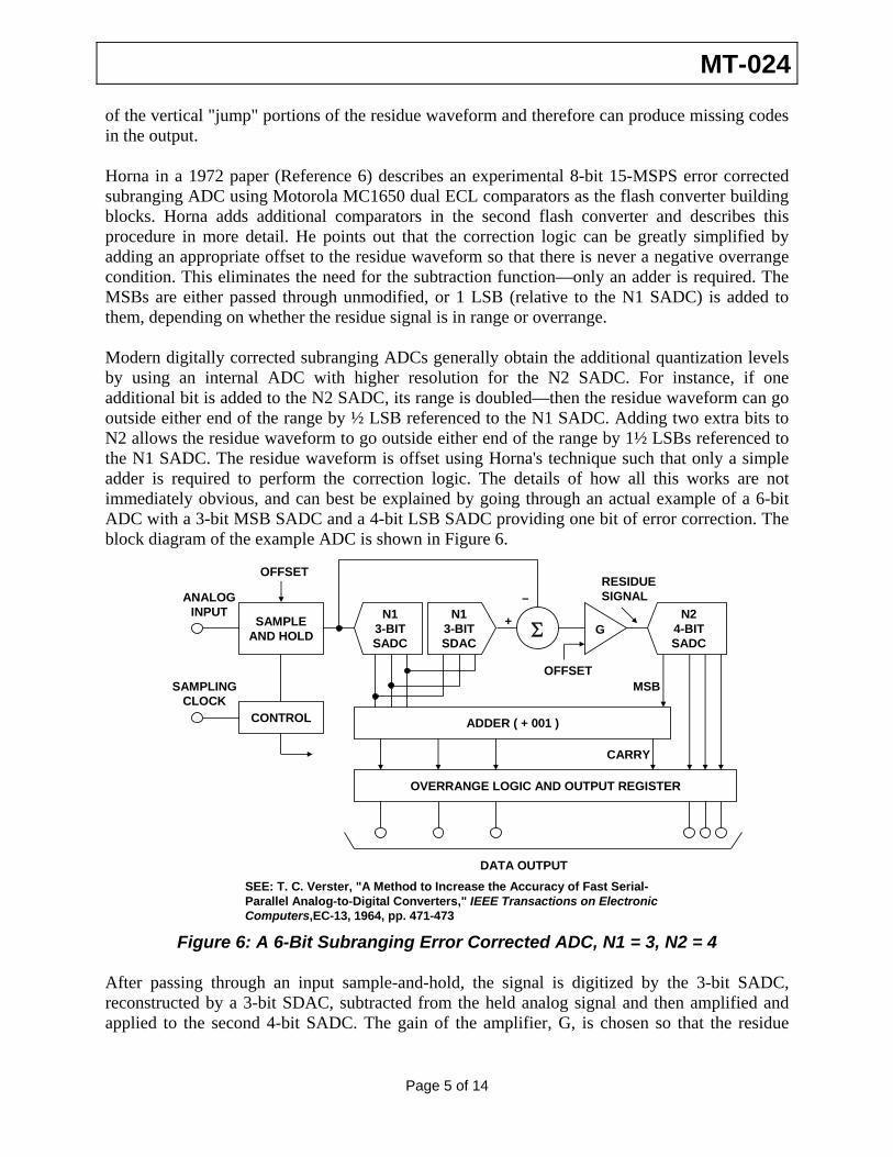
of the vertical "jump" portions of the residue waveform and therefore can produce missing codes in the output. Horna in a 1972 paper (Reference 6) describes an experimental 8-bit 15-MSPS error corrected subranging ADC using Motorola MC1650 dual ECL comparators as the flash converter building blocks. Horna adds additional comparators in the second flash converter and describes this procedure in more detail. He points out that the correction logic can be greatly simplified by adding an appropriate offset to the residue waveform so that there is never a negative overrange condition. This eliminates the need for the subtraction function—only an adder is required. The MSBs are either passed through unmodified, or 1 LSB (relative to the N1 SADC) is added to them, depending on whether the residue signal is in range or overrange. Modern digitally corrected subranging ADCs generally obtain the additional quantization levels by using an internal ADC with higher resolution for the N2 SADC. For instance, if one additional bit is added to the N2 SADC, its range is doubled—then the residue waveform can go outside either end of the range by ½ LSB referenced to the N1 SADC. Adding two extra bits to N2 allows the residue waveform to go outside either end of the range by 1½ LSBs referenced to the N1 SADC. The residue waveform is offset using Horna's technique such that only a simple adder is required to perform the correction logic. The details of how all this works are not immediately obvious, and can best be explained by going through an actual example of a 6-bit ADC with a 3-bit MSB SADC and a 4-bit LSB SADC providing one bit of error correction. The block diagram of the example ADC is shown in Figure 6.
SAMPLEAND HOLD Σ+
–
OVERRANGE LOGIC AND OUTPUT REGISTER
ANALOGINPUT
DATA OUTPUT
CONTROL
SAMPLINGCLOCK
ADDER ( + 001 )
RESIDUESIGNAL
MSB
CARRY
G
SEE: T. C. Verster, "A Method to Increase the Accuracy of Fast Serial-Parallel Analog-to-Digital Converters," IEEE Transactions on Electronic Computers,EC-13, 1964, pp. 471-473
OFFSET
OFFSET
N13-BITSADC
N13-BITSDAC
N24-BITSADC
Figure 6: A 6-Bit Subranging Error Corrected ADC, N1 = 3, N2 = 4 After passing through an input sample-and-hold, the signal is digitized by the 3-bit SADC, reconstructed by a 3-bit SDAC, subtracted from the held analog signal and then amplified and applied to the second 4-bit SADC. The gain of the amplifier, G, is chosen so that the residue
Page 5 of 14
MT-024
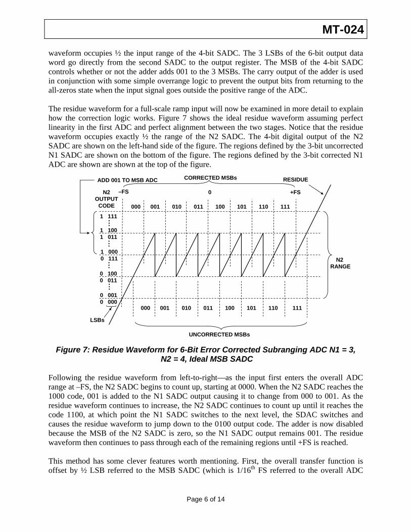
waveform occupies ½ the input range of the 4-bit SADC. The 3 LSBs of the 6-bit output data word go directly from the second SADC to the output register. The MSB of the 4-bit SADC controls whether or not the adder adds 001 to the 3 MSBs. The carry output of the adder is used in conjunction with some simple overrange logic to prevent the output bits from returning to the all-zeros state when the input signal goes outside the positive range of the ADC. The residue waveform for a full-scale ramp input will now be examined in more detail to explain how the correction logic works. Figure 7 shows the ideal residue waveform assuming perfect linearity in the first ADC and perfect alignment between the two stages. Notice that the residue waveform occupies exactly ½ the range of the N2 SADC. The 4-bit digital output of the N2 SADC are shown on the left-hand side of the figure. The regions defined by the 3-bit uncorrected N1 SADC are shown on the bottom of the figure. The regions defined by the 3-bit corrected N1 ADC are shown are shown at the top of the figure.
0 0010 000
0 1000 011
1 0000 111
1 1001 011
1 111000 001 010 011 100 101 110 111
N2RANGE
CORRECTED MSBs
N2OUTPUT
CODE
ADD 001 TO MSB ADC
–FS 0 +FS
RESIDUE
LSBs
000 001 010 011 100 101 110 111
UNCORRECTED MSBs
•••
•••
•••
•••
Figure 7: Residue Waveform for 6-Bit Error Corrected Subranging ADC N1 = 3, N2 = 4, Ideal MSB SADC
Following the residue waveform from left-to-right—as the input first enters the overall ADC range at –FS, the N2 SADC begins to count up, starting at 0000. When the N2 SADC reaches the 1000 code, 001 is added to the N1 SADC output causing it to change from 000 to 001. As the residue waveform continues to increase, the N2 SADC continues to count up until it reaches the code 1100, at which point the N1 SADC switches to the next level, the SDAC switches and causes the residue waveform to jump down to the 0100 output code. The adder is now disabled because the MSB of the N2 SADC is zero, so the N1 SADC output remains 001. The residue waveform then continues to pass through each of the remaining regions until +FS is reached. This method has some clever features worth mentioning. First, the overall transfer function is offset by ½ LSB referred to the MSB SADC (which is 1/16th FS referred to the overall ADC
Page 6 of 14
MT-024
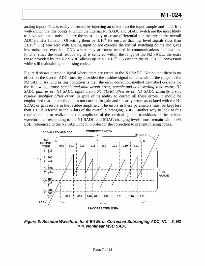
analog input). This is easily corrected by injecting an offset into the input sample-and-hold. It is well-known that the points at which the internal N1 SADC and SDAC switch are the most likely to have additional noise and are the most likely to create differential nonlinearity in the overall ADC transfer function. Offsetting them by 1/16th FS ensures that low level signals (less than ±1/16th FS) near zero volts analog input do not exercise the critical switching points and gives low noise and excellent DNL where they are most needed in communications applications. Finally, since the ideal residue signal is centered within the range of the N2 SADC, the extra range provided by the N2 SADC allows up to a ±1/16th FS error in the N1 SADC conversion while still maintaining no missing codes. Figure 8 shows a residue signal where there are errors in the N1 SADC. Notice that there is no effect on the overall ADC linearity provided the residue signal remains within the range of the N2 SADC. As long as this condition is met, the error correction method described corrects for the following errors: sample-and-hold droop error, sample-and-hold settling time error, N1 SADC gain error, N1 SADC offset error, N1 SDAC offset error, N1 SADC linearity error, residue amplifier offset error. In spite of its ability to correct all these errors, it should be emphasized that this method does not correct for gain and linearity errors associated with the N1 SDAC or gain errors in the residue amplifier. The errors in these parameters must be kept less than 1 LSB referred to the N-bits of the overall subranging ADC. Another way to look at this requirement is to realize that the amplitude of the vertical "jump" transitions of the residue waveform, corresponding to the N1 SADC and SDAC changing levels, must remain within ±½ LSB referenced to the N2 SADC input in order for the correction to prevent missing codes.
0 0010 000
0 1000 011
1 0000 111
1 1001 011
1 111000 001 010 011 100 101 110 111
N2RANGE
CORRECTED MSBs
N2OUTPUT
CODE
ADD 001 TO MSB ADCRESIDUE
–FS 0 +FS
LSBs
000 001 010 011 100 101 110 111
UNCORRECTED MSBs
•••
•••
•••
•••
Figure 8: Residue Waveform for 6-Bit Error Corrected Subranging ADC, N1 = 3, N2
= 4, Nonlinear MSB SADC
Page 7 of 14
MT-024
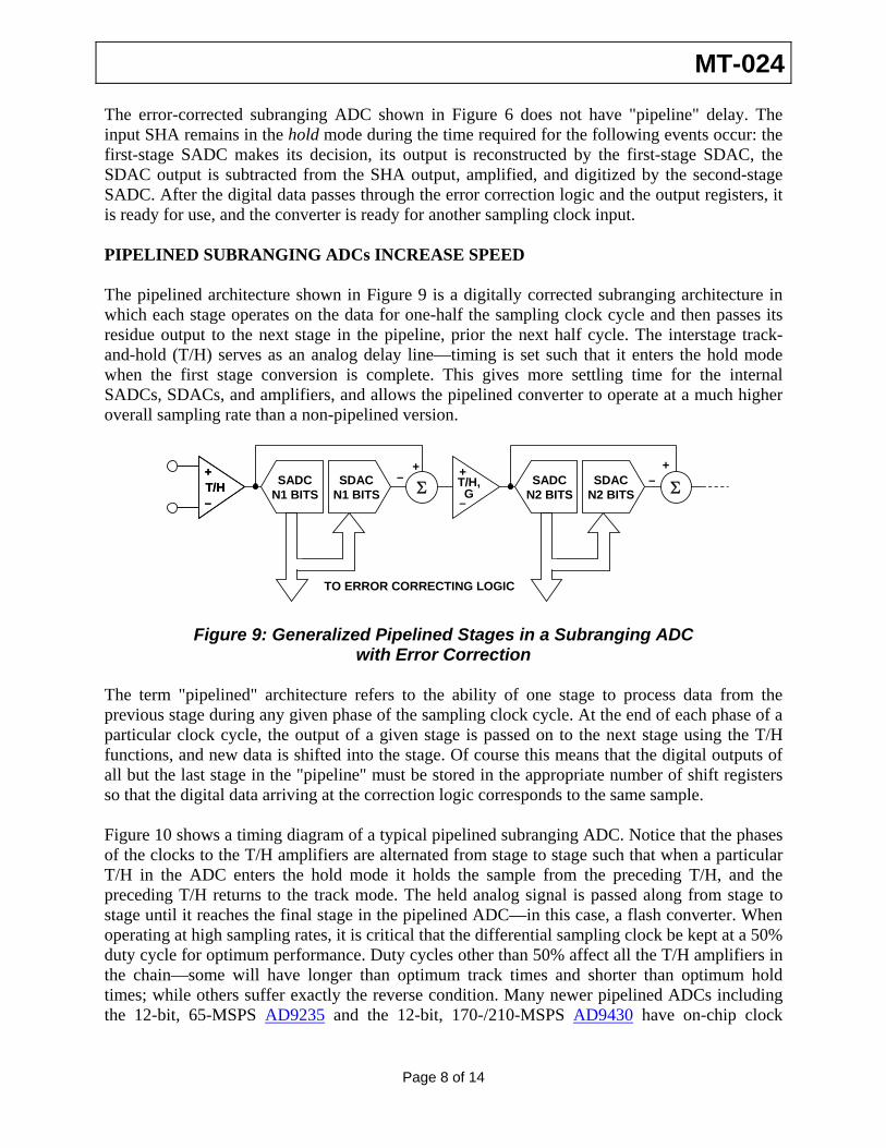
The error-corrected subranging ADC shown in Figure 6 does not have "pipeline" delay. The input SHA remains in the hold mode during the time required for the following events occur: the first-stage SADC makes its decision, its output is reconstructed by the first-stage SDAC, the SDAC output is subtracted from the SHA output, amplified, and digitized by the second-stage SADC. After the digital data passes through the error correction logic and the output registers, it is ready for use, and the converter is ready for another sampling clock input. PIPELINED SUBRANGING ADCs INCREASE SPEED The pipelined architecture shown in Figure 9 is a digitally corrected subranging architecture in which each stage operates on the data for one-half the sampling clock cycle and then passes its residue output to the next stage in the pipeline, prior the next half cycle. The interstage track-and-hold (T/H) serves as an analog delay line—timing is set such that it enters the hold mode when the first stage conversion is complete. This gives more settling time for the internal SADCs, SDACs, and amplifiers, and allows the pipelined converter to operate at a much higher overall sampling rate than a non-pipelined version.
SADCN1 BITS
SDACN1 BITST/H
+
–T/H+
–
+
–Σ
+– SADC
N2 BITSSDAC
N2 BITS Σ+
–
TO ERROR CORRECTING LOGIC
T/H,G
Figure 9: Generalized Pipelined Stages in a Subranging ADC with Error Correction
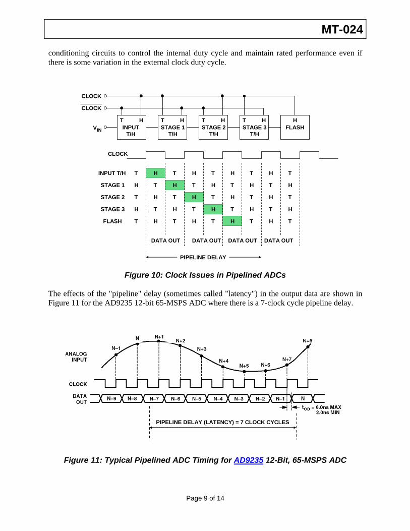
The term "pipelined" architecture refers to the ability of one stage to process data from the previous stage during any given phase of the sampling clock cycle. At the end of each phase of a particular clock cycle, the output of a given stage is passed on to the next stage using the T/H functions, and new data is shifted into the stage. Of course this means that the digital outputs of all but the last stage in the "pipeline" must be stored in the appropriate number of shift registers so that the digital data arriving at the correction logic corresponds to the same sample. Figure 10 shows a timing diagram of a typical pipelined subranging ADC. Notice that the phases of the clocks to the T/H amplifiers are alternated from stage to stage such that when a particular T/H in the ADC enters the hold mode it holds the sample from the preceding T/H, and the preceding T/H returns to the track mode. The held analog signal is passed along from stage to stage until it reaches the final stage in the pipelined ADC—in this case, a flash converter. When operating at high sampling rates, it is critical that the differential sampling clock be kept at a 50% duty cycle for optimum performance. Duty cycles other than 50% affect all the T/H amplifiers in the chain—some will have longer than optimum track times and shorter than optimum hold times; while others suffer exactly the reverse condition. Many newer pipelined ADCs including the 12-bit, 65-MSPS AD9235 and the 12-bit, 170-/210-MSPS AD9430 have on-chip clock
Page 8 of 14
MT-024
conditioning circuits to control the internal duty cycle and maintain rated performance even if there is some variation in the external clock duty cycle.
FLASH
CLOCK
CLOCK
VIN
TINPUT
T/HSTAGE 1
T/HSTAGE 2
T/HSTAGE 3
T/H
H T H T H T H H
CLOCK
INPUT T/H
STAGE 1
STAGE 2
STAGE 3
FLASH
T H T H T H T H
H H T H T HT T
T H T H T H T H
H H T H T HT T
DATA OUT DATA OUT DATA OUT DATA OUT
T H T H T H T
H
T
H
T
H T
PIPELINE DELAY
Figure 10: Clock Issues in Pipelined ADCs The effects of the "pipeline" delay (sometimes called "latency") in the output data are shown in Figure 11 for the AD9235 12-bit 65-MSPS ADC where there is a 7-clock cycle pipeline delay.
PIPELINE DELAY (LATENCY) = 7 CLOCK CYCLES
Figure 11: Typical Pipelined ADC Timing for AD9235 12-Bit, 65-MSPS ADC
Page 9 of 14
MT-024
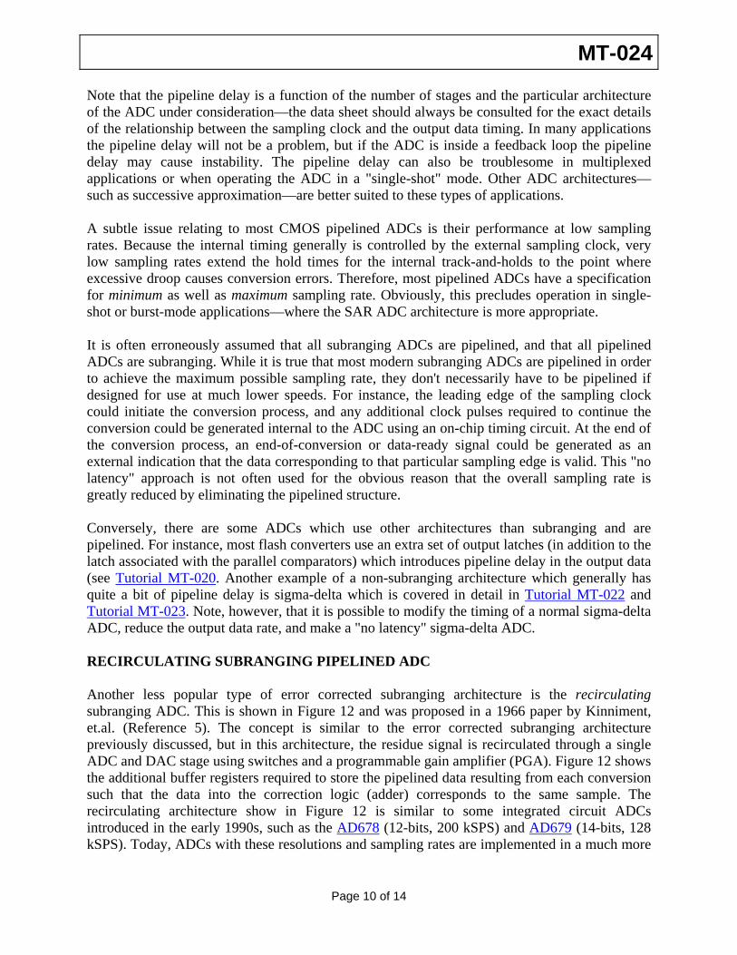
Note that the pipeline delay is a function of the number of stages and the particular architecture of the ADC under consideration—the data sheet should always be consulted for the exact details of the relationship between the sampling clock and the output data timing. In many applications the pipeline delay will not be a problem, but if the ADC is inside a feedback loop the pipeline delay may cause instability. The pipeline delay can also be troublesome in multiplexed applications or when operating the ADC in a "single-shot" mode. Other ADC architectures—such as successive approximation—are better suited to these types of applications. A subtle issue relating to most CMOS pipelined ADCs is their performance at low sampling rates. Because the internal timing generally is controlled by the external sampling clock, very low sampling rates extend the hold times for the internal track-and-holds to the point where excessive droop causes conversion errors. Therefore, most pipelined ADCs have a specification for minimum as well as maximum sampling rate. Obviously, this precludes operation in single-shot or burst-mode applications—where the SAR ADC architecture is more appropriate. It is often erroneously assumed that all subranging ADCs are pipelined, and that all pipelined ADCs are subranging. While it is true that most modern subranging ADCs are pipelined in order to achieve the maximum possible sampling rate, they don't necessarily have to be pipelined if designed for use at much lower speeds. For instance, the leading edge of the sampling clock could initiate the conversion process, and any additional clock pulses required to continue the conversion could be generated internal to the ADC using an on-chip timing circuit. At the end of the conversion process, an end-of-conversion or data-ready signal could be generated as an external indication that the data corresponding to that particular sampling edge is valid. This "no latency" approach is not often used for the obvious reason that the overall sampling rate is greatly reduced by eliminating the pipelined structure. Conversely, there are some ADCs which use other architectures than subranging and are pipelined. For instance, most flash converters use an extra set of output latches (in addition to the latch associated with the parallel comparators) which introduces pipeline delay in the output data (see Tutorial MT-020. Another example of a non-subranging architecture which generally has quite a bit of pipeline delay is sigma-delta which is covered in detail in Tutorial MT-022 and Tutorial MT-023. Note, however, that it is possible to modify the timing of a normal sigma-delta ADC, reduce the output data rate, and make a "no latency" sigma-delta ADC. RECIRCULATING SUBRANGING PIPELINED ADC Another less popular type of error corrected subranging architecture is the recirculating subranging ADC. This is shown in Figure 12 and was proposed in a 1966 paper by Kinniment, et.al. (Reference 5). The concept is similar to the error corrected subranging architecture previously discussed, but in this architecture, the residue signal is recirculated through a single ADC and DAC stage using switches and a programmable gain amplifier (PGA). Figure 12 shows the additional buffer registers required to store the pipelined data resulting from each conversion such that the data into the correction logic (adder) corresponds to the same sample. The recirculating architecture show in Figure 12 is similar to some integrated circuit ADCs introduced in the early 1990s, such as the AD678 (12-bits, 200 kSPS) and AD679 (14-bits, 128 kSPS). Today, ADCs with these resolutions and sampling rates are implemented in a much more
Page 10 of 14
MT-024
efficient and cost effective manner using the successive approximation architecture discussed in Tutorial MT-021.
SAMPLEAND HOLD PGAΣ
3-BITFLASH
ADC
3-BITDAC
+
–
REG.
REG. REG.
REG. REG. REG.
ADDER
OUTPUT REGISTER
CONTROL
ANALOGINPUT
SAMPLINGCLOCK
Adapted from: D.J. Kinniment, D. Aspinall, and D.B.G. Edwards,"High-Speed Analogue-Digital Converter," IEE Proceedings, Vol. 113, pp. 2061-2069, Dec. 1966
DATA OUTPUT
Figure 12: Kinniment, et. al., 1966 Pipelined 7-bit, 9-MSPS Recirculating ADC Architecture
MODERN MONOLITHIC PIPELINED ADCs FOR VIDEO AND IMAGE PROCESSING The discussion of error corrected pipelined ADCs concludes with a few examples of modern integrated circuit implementations of the popular architecture. These examples show the flexibility of the technique in optimizing ADC performance at different resolutions, sampling rates, power dissipation, etc. The video market currently uses ADCs with resolutions of 8 to 12-bits, and sampling rates from 54 MSPS to 140 MSPS. Most of these ADCs are now integrated into chips which perform further digital signal processing, such as the conversion between the various existing video standards (composite, RGB, Y/C, Y/Pb/Pr). These ICs perform a considerable amount of digital processing as shown in the ADV-Series Video Decoders from Analog Devices. The ADC architecture is generally pipelined, the process CMOS, and total package power dissipation ranges from 250 mW to 600 mW. Another family of similar products is used in CCD Image Processing applications for cameras and camcorders. In the current "stand-alone" 8-bit ADC market, the pipelined architecture is implemented in the 8-bit 250 MSPS, AD9480 (LVDS outputs) and AD9481 (demuxed CMOS outputs) which dissipate 700 mW and 600 mW, respetively.
Page 11 of 14
MT-024
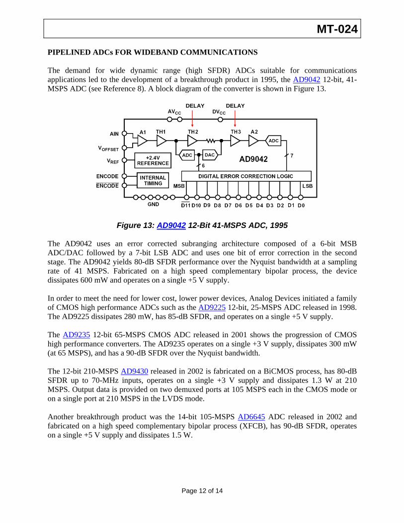
PIPELINED ADCs FOR WIDEBAND COMMUNICATIONS The demand for wide dynamic range (high SFDR) ADCs suitable for communications applications led to the development of a breakthrough product in 1995, the AD9042 12-bit, 41-MSPS ADC (see Reference 8). A block diagram of the converter is shown in Figure 13. DELAY DELAY
Figure 13: AD9042 12-Bit 41-MSPS ADC, 1995 The AD9042 uses an error corrected subranging architecture composed of a 6-bit MSB ADC/DAC followed by a 7-bit LSB ADC and uses one bit of error correction in the second stage. The AD9042 yields 80-dB SFDR performance over the Nyquist bandwidth at a sampling rate of 41 MSPS. Fabricated on a high speed complementary bipolar process, the device dissipates 600 mW and operates on a single +5 V supply. In order to meet the need for lower cost, lower power devices, Analog Devices initiated a family of CMOS high performance ADCs such as the AD9225 12-bit, 25-MSPS ADC released in 1998. The AD9225 dissipates 280 mW, has 85-dB SFDR, and operates on a single +5 V supply. The AD9235 12-bit 65-MSPS CMOS ADC released in 2001 shows the progression of CMOS high performance converters. The AD9235 operates on a single +3 V supply, dissipates 300 mW (at 65 MSPS), and has a 90-dB SFDR over the Nyquist bandwidth. The 12-bit 210-MSPS AD9430 released in 2002 is fabricated on a BiCMOS process, has 80-dB SFDR up to 70-MHz inputs, operates on a single +3 V supply and dissipates 1.3 W at 210 MSPS. Output data is provided on two demuxed ports at 105 MSPS each in the CMOS mode or on a single port at 210 MSPS in the LVDS mode. Another breakthrough product was the 14-bit 105-MSPS AD6645 ADC released in 2002 and fabricated on a high speed complementary bipolar process (XFCB), has 90-dB SFDR, operates on a single +5 V supply and dissipates 1.5 W.
Page 12 of 14
MT-024
THE LATEST IN PIPELINED ADCs The 12-bit high speed ADC segment has seen significant improvements in speed, power, and performance, as reflected by the AD9236 12-bit 80 MSPS CMOS ADC with only 360 mW of power dissipation. The AD9236 is part of the pin-compatible family which includes the AD9215 (10-bit, 105 MSPS), AD9235 (12-bit, 65 MSPS) and the AD9245 (14-bit, 80 MSPS). These pin-compatible devices allow easy migration from 10-bits to 14-bits and sampling rates from 20 MSPS to higher rates. In addition to single ADCs, dual ADCs and quad ADCs are available, including the AD9229 quad 12-bit 65 MSPS ADC with LVDS outputs. Power dissipation is 1.5 W, and the part is ideally suited for high density applications such as medical ultrasound. In the 14-bit communications ADC area, the AD9244 14-bit, 65 MSPS is optimized for Nyquist input signals (dc to fs/2), has an SFDR of 86 dB, and dissipates only 550 mW on a CMOS process. For higher input bandwidths and IF sampling, the AD9445 14-bit, 125 MSPS ADC is available with an SFDR of 95 dB (measured with a 170 MHz input), and a power dissipation of 2.6 W. The AD9445 is designed on a BiCMOS process. Also for communications applications, the AD9446 16-bit, 100 MSPS ADC is optimized for high SNR (84 dB), dissipates 2.8 W, and is also designed on a BiCMOS process. SUMMARY The pipelined subranging ADC architecture virtually dominates where sampling rates of greater than a few MHz are required. There is some overlap between the SAR architecture and the pipelined architecture in the 2 to 5 MSPS region, but the application should easily dictate which architecture is more appropriate. Resolutions from 8- to 16-bits are available in a variety of packages and configurations (signals, duals, triples, quads, etc.). Fine-line CMOS is by far the most popular process for these converters, and BiCMOS is used where it is necessary to obtain the ultimate in dynamic performance. For a given sampling rate and resolution, pipelined ADCs are often differentiated by their dynamic performance. For example, the AD9244 14-bit, 65 MSPS ADC is optimized to handle input signals from dc to Nyquist (fs/2) and dissipates only 550 mW. If signals in higher Nyquist zones must be processed, the AD9445 14-bit, 125 MSPS ADC is available at 2.6 W on a more expensive BiCMOS process. Selecting the proper pipelined ADC for a particular application requires a thorough understanding of not only system requirements but also a working knowledge of the architecture and the possible tradeoffs available. Simply treating the ADC as a "black box" often leads to the wrong choice.
Page 13 of 14
Page 14 of 14
MT-024
REFERENCES 1. R. Staffin and R. D. Lohman, "Signal Amplitude Quantizer," U.S. Patent 2,869,079, filed December 19, 1956,
issued January 13, 1959. (describes flash and subranging conversion using tubes and transistors). 2. H. R. Schindler, "Using the Latest Semiconductor Circuits in a UHF Digital Converter," Electronics, August
1963, pp. 37-40. (describes a 6-bit 50-MSPS subranging ADC using three 2-bit tunnel diode flash converters). 3. T. C. Verster, "A Method to Increase the Accuracy of Fast Serial-Parallel Analog-to-Digital Converters," IEEE
Transactions on Electronic Computers, EC-13, 1964, pp. 471-473. (one of the first references to the use of error correction in a subranging ADC).
4. G. G. Gorbatenko, "High-Performance Parallel-Serial Analog to Digital Converter with Error Correction," IEEE
National Convention Record, New York, March 1966. (another early reference to the use of error correction in a subranging ADC).
5. D. J. Kinniment, D. Aspinall, and D.B.G. Edwards, "High-Speed Analogue-Digital Converter," IEE
Proceedings, Vol. 113, pp. 2061-2069, Dec. 1966. (a 7-bit 9MSPS three-stage pipelined error corrected converter is described based on recircuilating through a 3-bit stage three times. Tunnel (Esaki) diodes are used for the individual comparators. The article also shows a proposed faster pipelined 7-bit architecture using three individual 3-bit stages with error correction. The article also describes a fast bootstrapped diode-bridge sample-and-hold circuit).
6. O. A. Horna, "A 150Mbps A/D and D/A Conversion System," Comsat Technical Review, Vol. 2, No. 1, pp. 52-
57, 1972. (a detailed description and analysis of a subranging ADC with error correction). 7. J. L. Fraschilla, R. D. Caveney, and R. M. Harrison, "High Speed Analog-to-Digital Converter," U.S. Patent
3,597,761, filed Nov. 14, 1969, issued Aug. 13, 1971. (Describes an 8-bit, 5-MSPS subranging ADC with switched references to second comparator bank).
8. Roy Gosser and Frank Murden, "A 12-bit 50MSPS Two-Stage A/D Converter," 1995 ISSCC Digest of
Technical Papers, p. 278. (a description of the AD9042 error corrected subranging ADC using MagAMP stages for the internal ADCs).
9. Walt Kester, Analog-Digital Conversion, Analog Devices, 2004, ISBN 0-916550-27-3, Chapter 3. Also
available as The Data Conversion Handbook, Elsevier/Newnes, 2005, ISBN 0-7506-7841-0, Chapter 3. Copyright 2009, Analog Devices, Inc. All rights reserved. Analog Devices assumes no responsibility for customer product design or the use or application of customers’ products or for any infringements of patents or rights of others which may result from Analog Devices assistance. All trademarks and logos are property of their respective holders. Information furnished by Analog Devices applications and development tools engineers is believed to be accurate and reliable, however no responsibility is assumed by Analog Devices regarding technical accuracy and topicality of the content provided in Analog Devices Tutorials.