Embed Size (px)
Citation preview

Physics-based compact
model for ultimate FinFETs
Ashkhen YESAYAN, Nicolas CHEVILLON, Fabien PREGALDINY,
Morgan MADEC, Christophe LALLEMENT, Jean-Michel SALLESE

N. CHEVILLON [email protected] 8 April 2011MOS-AK2
Research team and collaboration
Professor - Christophe LALLEMENT
Associate professor - Fabien PREGALDINY
Associate professor - Morgan MADECCompact modeling
of advanced devicesPost-doc – Ashkhen YESAYAN - left in Dec. 2010
PhD student - Nicolas CHEVILLON
Collaboration
Dr. Jean-Michel SALLESE
LEG, EPFL

N. CHEVILLON [email protected] 8 April 2011MOS-AK3
Outline
Mobility modeling3
Short-channel effects modeling2
Introduction1
Quantum mechanical effect modeling4
Transcapacitance modeling5
Doped DG MOSFET modeling6

N. CHEVILLON [email protected] 8 April 2011MOS-AK4
FinFET transistor
One of the best candidate to extend the CMOS technology.
Needs of designers for advanced circuit simulation:
(COMON European project)
• a physics-based FinFET compact model
• a parameter extraction methodology
L: channel length
WSi: silicon width
HSi: silicon height
tox: oxide thickness

N. CHEVILLON [email protected] 8 April 2011MOS-AK
Model accounts for small-geometry effects [3]:
• Short-channel effects (SCE), drain-induced barrier lowering (DIBL)
• Subthreshold swing degradation
• Drain saturation voltage and channel length modulation (CLM)
• Mobility degradation
• Quantum mechanical effects (QME)
5
Physics-based FinFET compact model
Physics-based long-channel DG MOSFET model [1]
• Extension of the undoped model to high doping [2]
[1] J.-M. Sallese, F. Krummenacher, F. Prégaldiny, C. Lallement, A. Roy and C. Enz, “A design oriented charge-based current model for
symmetric DG MOSFET and its correlation with the EKV formalism,” Solid-State Electronics, vol. 49, no. 3, pp.485-489, Mar 2005.
Transcapacitance modeling for small-geometry [3]
[3] A. Yesayan, F. Prégaldiny, N. Chevillon, C. Lallement and J.-M. Sallese, “Physics-based compact model for ultra-scaled FinFETs,”
Solid-State Electronics, Article in Press, April 2011.
[2] J.-M. Sallese, N. Chevillon, F. Prégaldiny, C. Lallement and B. Iñiguez, “The equivalent-thickness concept for doped symmetric DG
MOSFETs,” IEEE Transactions on Electron Devices, vol. 57, no. 11, pp.2917-2924, Nov 2010.

N. CHEVILLON [email protected] 8 April 2011MOS-AK6
Range of validity
Gate length (L) : down to 25 nm
Silicon width (WSi) : down to 3 nm
Silicon height (HSi): down to 50 nm
Gate oxide thickness (tox) : 1.5 nm
Top oxide thickness (ttop) : 50nm
Channel doping (Nch) : intrinsic to 1017 cm-3 and high doping*
Source/Drain doping (Nsd) : 51021 cm-3
*: only for long channel devices
N. CHEVILLON [email protected] 8 April 2011MOS-AK7
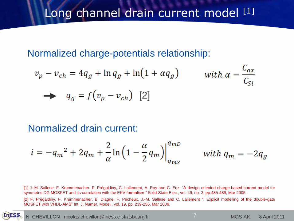
Long channel drain current model [1]
Normalized drain current:
Normalized charge-potentials relationship:
[2] F. Prégaldiny, F. Krummenacher, B. Diagne, F. Pêcheux, J.-M. Sallese and C. Lallement “, Explicit modelling of the double-gate
MOSFET with VHDL-AMS” Int. J. Numer. Model., vol. 19, pp. 239-256, Mar 2006.
[1] J.-M. Sallese, F. Krummenacher, F. Prégaldiny, C. Lallement, A. Roy and C. Enz, “A design oriented charge-based current model for
symmetric DG MOSFET and its correlation with the EKV formalism,” Solid-State Elec., vol. 49, no. 3, pp.485-489, Mar 2005.
[2]

N. CHEVILLON [email protected] 8 April 2011MOS-AK8
Study of the minimum surface potential
Cross-section
of FinFET
Study in:
- classic physics
- weak inversion

N. CHEVILLON [email protected] 8 April 2011MOS-AK9
Current model for ultra-short channels [1] (1/2)
Correction of the gate voltage:
Drain current model:
[1] A. Yesayan, F. Prégaldiny, N. Chevillon, C. Lallement and J.-M. Sallese, “Physics-based compact model for ultra-scaled FinFETs,”
Solid-State Electronics, Article in Press, April 2011.

N. CHEVILLON [email protected] 8 April 2011MOS-AK10
Current model for ultra-short channels (2/2)
Potential Expression in the channel in the subthreshold region [1]:
[1] X. Liang, and Y. Taur, “A 2-D Analytical solution for SCEs in DG MOSFETs,” IEEE Trans. Electron Devices, vol. 51, no. 8, pp. 1385-
1391, August 2004.
In weak inversion:
• in the long-channel case,
• in the short-channel case,
In strong inversion, analytical expression is negligeable w.r.t ,
No need of smoothing function between weak and strong inversion.
valid for L > 1.5 SiW
General scaling length

N. CHEVILLON [email protected] 8 April 2011MOS-AK11
Mobility model [1]
Term of mobility degradation
for the short channels in
weak inversion
Terms of mobility degradation
in strong inversion
: long-channel low field mobility
: transversal electric field in weak inversion
: transversal electric field in high inversion
: parameters to be extracted
[2] F. Lime, B. Iñiguez and O. Moldovan, “A quasi-two dimentional compact drain-current model for undoped symmetric double-gate
MOSFETs including short-channel effects,” IEEE Trans. Electron Devices, vol. 55, no. 6, pp. 1441-1448, June 2008.
Transversal mobility:
Total mobility model and channel length modulation model taken from [2]
: normalizing factor
[1] A. Yesayan, F. Prégaldiny, N. Chevillon, C. Lallement and J.-M. Sallese, “Physics-based compact model for ultra-scaled FinFETs,”
Solid-State Electronics, Article in Press, April 2011.

N. CHEVILLON [email protected] 8 April 2011MOS-AK12
Quantum mechanical effects [1] (1/3)
Quantum shift of the first energy level:
[1] A. Yesayan, F. Prégaldiny, N. Chevillon, C. Lallement and J.-M. Sallese, “Physics-based compact model for ultra-scaled FinFETs,”
Solid-State Electronics, Article in Press, April 2011.
E0
WSi
E1
EC
Structural confinement
E0
E1
WSi
EC
Electrical confinement
Principle of the quantum mechanical effects modeling

N. CHEVILLON [email protected] 8 April 2011MOS-AK13
Quantum mechanical effects (2/3)
Inclusion of the term of structural confinement in the
charge-potential relationship
Inclusion of the term of electrical confinement
in the charge-potential relationship
Modeling of the quantum shift as a correction to surface potential:
: elementary electronic charge
: thermal voltage
: effective mass of electrons in the channel length direction
N. CHEVILLON [email protected] 8 April 2011MOS-AK14
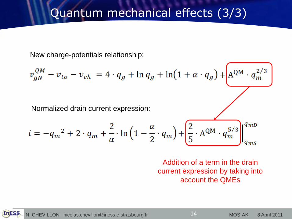
Quantum mechanical effects (3/3)
New charge-potentials relationship:
Normalized drain current expression:
Addition of a term in the drain
current expression by taking into
account the QMEs

N. CHEVILLON [email protected] 8 April 2011MOS-AK15
Results of the static model
Id(Vd) current curves
Symbols: Quantum 3D simulations with CVT mobility model
Lines: Compact model
Id(Vg) current curves

N. CHEVILLON [email protected] 8 April 2011MOS-AK16
Transcapacitance modeling [1]
Normalized total charge calculation according to the
channel charge partition proposed by Ward
Transcapacitance definitions:
[1] A. Yesayan, F. Prégaldiny, N. Chevillon, C. Lallement and J.-M. Sallese, “Physics-based compact model for ultra-scaled FinFETs,”
Solid-State Electronics, Article in Press, April 2011.
Charge-based expressions for the transcapacitances

N. CHEVILLON [email protected] 8 April 2011MOS-AK17
Transcapacitance modeling [1]
Modeling of the electrical confinement by approximated according
to a taylor series,
Modeling of the structural confinement by in
the calculation of the charge density .
within a new definition of the gate oxide capacitance
[1] A. Yesayan, F. Prégaldiny, N. Chevillon, C. Lallement and J.-M. Sallese, “Physics-based compact model for ultra-scaled FinFETs,”
Solid-State Electronics, Article in Press, April 2011.

N. CHEVILLON [email protected] 8 April 2011MOS-AK18
Results of the dynamic model
Symbols: Quantum 3D simulations with constant mobility
Lines: Compact model
Cgg(Vg) of long channel Cgg(Vg) of short channel
N. CHEVILLON [email protected] 8 April 2011MOS-AK19
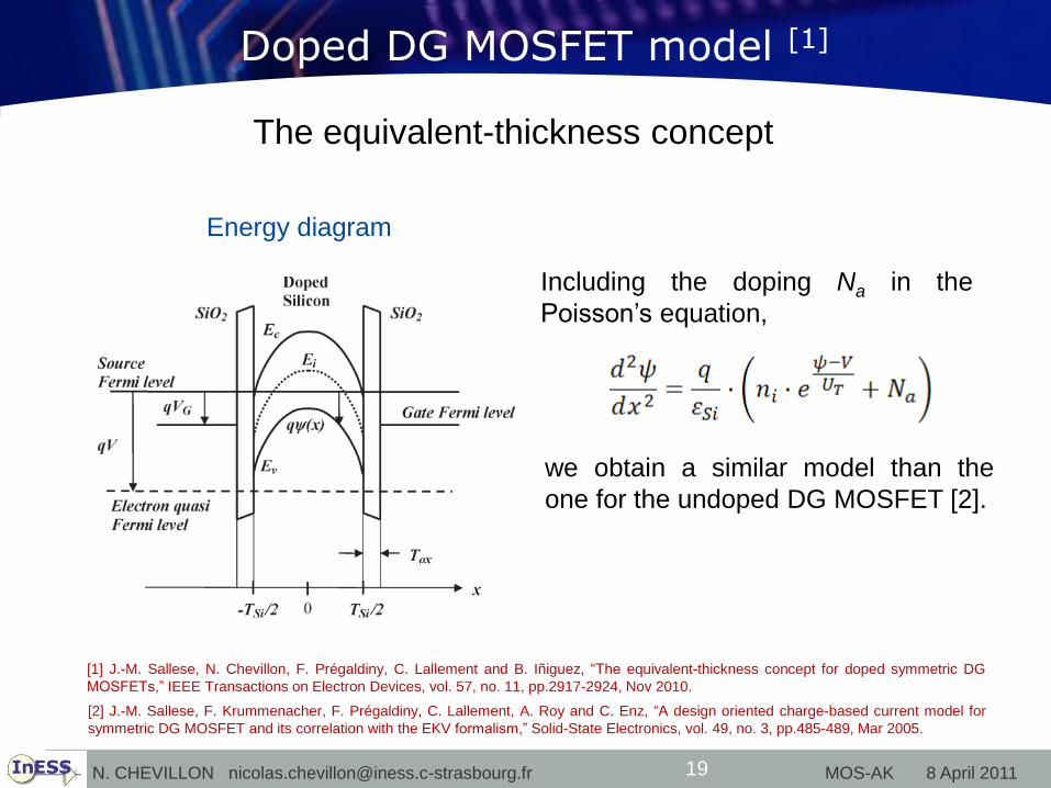
Doped DG MOSFET model [1]
The equivalent-thickness concept
Including the doping Na in the
Poisson’s equation,
Energy diagram
[2] J.-M. Sallese, F. Krummenacher, F. Prégaldiny, C. Lallement, A. Roy and C. Enz, “A design oriented charge-based current model for
symmetric DG MOSFET and its correlation with the EKV formalism,” Solid-State Electronics, vol. 49, no. 3, pp.485-489, Mar 2005.
[1] J.-M. Sallese, N. Chevillon, F. Prégaldiny, C. Lallement and B. Iñiguez, “The equivalent-thickness concept for doped symmetric DG
MOSFETs,” IEEE Transactions on Electron Devices, vol. 57, no. 11, pp.2917-2924, Nov 2010.
we obtain a similar model than the
one for the undoped DG MOSFET [2].

N. CHEVILLON [email protected] 8 April 2011MOS-AK20
Doped DG MOSFET model [1]
The equivalent-thickness concept
Charge-potentials relationship
[1] J.-M. Sallese, N. Chevillon, F. Prégaldiny, C. Lallement and B. Iñiguez, “The equivalent-thickness concept for doped symmetric DG
MOSFETs,” IEEE Transactions on Electron Devices, vol. 57, no. 11, pp.2917-2924, Nov 2010.

N. CHEVILLON [email protected] 8 April 2011MOS-AK21
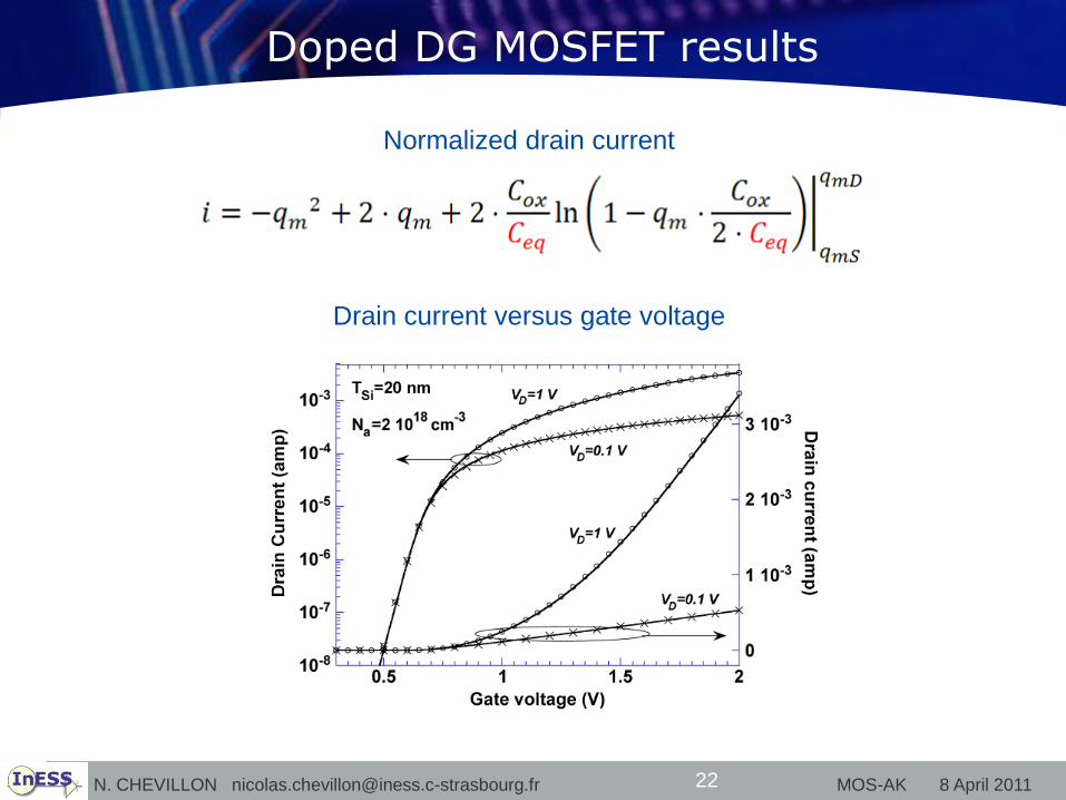
Doped DG MOSFET results
Equivalent thickness Mobile charge density
Exact analytical relationship between the equivalent thickness and the doping
Tsi = 40 nm
20 nm
10 nm
N. CHEVILLON [email protected] 8 April 2011MOS-AK22
Doped DG MOSFET results
Drain current versus gate voltage
Normalized drain current

N. CHEVILLON [email protected] 8 April 2011MOS-AK23
Electrical parameter number of the model
Effect Previous model [1,2] Present model [3]
Roll-off (SCE), DIBL
Subthreshold Slope (SS)
18 0
Channel Length
Modulation (CLM)
1 1
Mobility - 2
Quantification (QME) 9 0
Overlap capacitance - 1
All 28 4
[1] M. Tang, F. Prégaldiny, C. Lallement, J.-M. Sallese, “Explicit compact model for ultranarrow body FinFETs” IEEE Trans. Electron
Devices, vol. 56, no. 7, pp.1543-1547, Jul 2009.
[2] N. Chevillon, M. Tang, F. Prégaldiny, C. Lallement et M. Madec, “FinFET compact modeling and parameter extraction,” 16th IEEE
MIXDES., pp.55-60, Juin 2009.
[3] A. Yesayan, F. Prégaldiny, N. Chevillon, C. Lallement and J.-M. Sallese, “Physics-based compact model for ultra-scaled FinFETs,”
Solid-State Electronics, Article in Press, April 2011.
N. CHEVILLON [email protected] 8 April 2011MOS-AK24
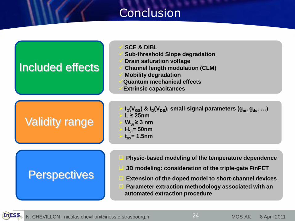
Conclusion
SCE & DIBL
Sub-threshold Slope degradation
Drain saturation voltage
Channel length modulation (CLM)
Mobility degradation
Quantum mechanical effects
Extrinsic capacitances
Included effects
Validity range
ID(VGS) & ID(VDS), small-signal parameters (gm, gds, …)
L ≥ 25nm
WSi ≥ 3 nm
HSi= 50nm
tox= 1.5nm
Perspectives
Physic-based modeling of the temperature dependence
3D modeling: consideration of the triple-gate FinFET
Extension of the doped model to short-channel devices
Parameter extraction methodology associated with an
automated extraction procedure
A. Yesayan, F. Prégaldiny, N. Chevillon, C. Lallement and J.-M. Sallese, “Physics-based compact model for
ultra-scaled FinFETs,” Solid-State Electronics, Article in Press, April 2011.
J.-M. Sallese, N. Chevillon, F. Prégaldiny, C. Lallement and B. Iñiguez, “The equivalent-thickness concept
for doped symmetric DG MOSFETs,” IEEE Transactions on Electron Devices, vol. 57, no. 11, pp.2917-2924,
Nov 2010.
Major publications:
J.-M. Sallese, F. Krummenacher, F. Prégaldiny, C. Lallement, A. Roy and C. Enz, “A design oriented charge-
based current model for symmetric DG MOSFET and its correlation with the EKV formalism,” Solid-State
Electronics, vol. 49, no. 3, pp.485-489, Mar 2005.