Embed Size (px)
Citation preview
Photonics
High Efficiency Organic Multilayer Photodetectors based on Singlet Fission .........................................................................................................................................................................................PH.1
Neodymium for Infrared Luminescent Solar Concentrator .........................................................................................................................PH.2
Efficiently Coupling Light to Superconducting Nanowire Single-photon Detectors .........................................................................PH.3
Guided-wave Devices for Holographic Video Display ...................................................................................................................................PH.4
Exciton-exciton Annihilation in Organic Polariton Microcavities ..............................................................................................................PH.5
Heterojunction Photovoltaics Using Printed Colloidal Quantum Dots as the Photosensitive Layer .............................................PH.6
Patterned Organic Microcavities for Confinement of Exciton-Polaritons ...............................................................................................PH.7
Heterojunction Photodetector Consisting of Metal-oxide and Colloidal Quantum-dot Thin Films...............................................PH.8
Heterojunction Photoconductors for Chemical Detection ..........................................................................................................................PH.9
Multi-layer Heterojunction Photoconductors ..................................................................................................................................................PH.10
3-molecular-layers-thick J-aggregate Photoconductor ................................................................................................................................PH.11
Strong Light-matter Coupling Using a Robust Non-cyanine Dye J-aggregate Material ....................................................................PH.12
Low-threshold Coherently-coupled Organic VCSEL ......................................................................................................................................PH.13
Electroluminescence from Phosphor-doped Nanocrystals .........................................................................................................................PH.14
High-efficiency, Low-cost Photovoltaics using III-V on Silicon Tandem Cells ........................................................................................PH.15
Co-axial Integration of III-V Ridge-waveguide Gain Elements with SiOxNy Waveguides on Silicon ................................................PH.16
Light-proof Electrodes for In-situ Monitoring of Neural Function ...........................................................................................................PH.17
Low-threshold Vertical Cavity Surface-emitting Lasers Recess- integrated within Silicon CMOS Integrated Circuits .............PH.18
Micro-cleaved Laser Diode Platelets Integrated on Silicon .........................................................................................................................PH.19
Waveguide Micro-probes for Optical Control of Excitable Cells ...............................................................................................................PH.20
Development of Terahertz Quantum-cascade Lasers ...................................................................................................................................PH.21
Ge-based Thermo-photovoltaic Cells .................................................................................................................................................................PH.22
Cavity-enhanced Photosensitivity in Chalcogenide Glass ...........................................................................................................................PH.23
Polycrystalline Germanium for Use in CMOS-compatible Photodetectors ...........................................................................................PH.24
Room-temperature Direct-band-gap Electroluminescence from Ge-on-Si Light-emitting Diodes ...............................................PH.25
Mid-IR Light Sources ...............................................................................................................................................................................................PH.26
Modulators for Arbitrary Optical Waveform Generation .............................................................................................................................PH.27
Nanoelectromechanically Actuated Optical Switches ..................................................................................................................................PH.28
Novel Active Materials for Optical Sources .......................................................................................................................................................PH.29
Photonic Crystal Applications ..............................................................................................................................................................................PH.30
Photonic Integrated Circuits for Ultrafast Optical Logic ..............................................................................................................................PH.31
Tunable Diode-laser Photoacoustic Spectroscopy .........................................................................................................................................PH.32
Deep Submicron CMOS Photonics ......................................................................................................................................................................PH.33
Ensuring Precision of Overlay in Photonic-crystal Lithography .................................................................................................................PH.34
Nanofabrication of Optical-microring Filter Banks for Integrated Photonic Systems .........................................................................PH.35
Localized-Substrate-Removal Technique Enabling Strong-Confinement Microphotonics in Bulk-Silicon CMOS .....................PH.36
Three-Dimensional Photonic Crystals In Si3N4 and Si by Assembly of Prepatterned Membranes ..................................................PH.37
Correction of Intrafield Distortion in Scanning-Electron-Beam Lithography and Confirmation via Optical Ring-Resonator Filters .............................................................................................................................................................................PH.38
Microscopy Beyond the Diffraction Limit Using Absorbance Modulation .............................................................................................PH.39
PH.1 MICROSYSTEMS TECHNOLOGY LABORATORIES ANNUAL RESEARCH REPORT 2009 PHotonics
PHotonics
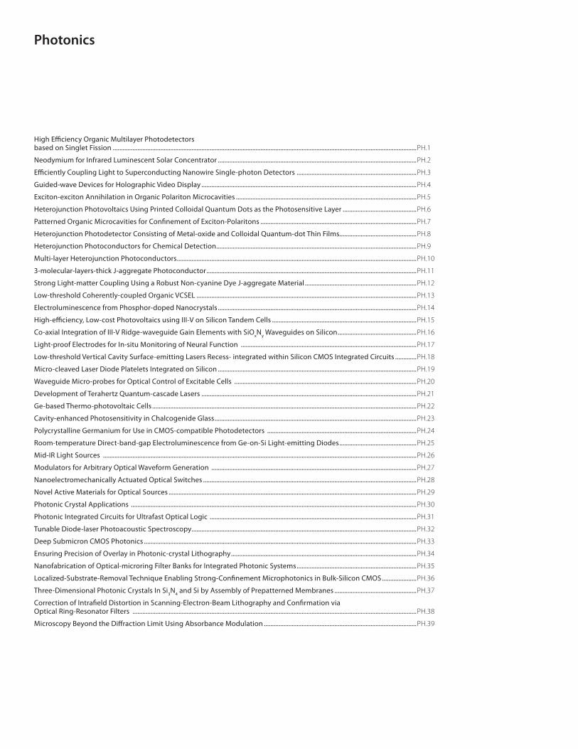
High Efficiency organic Multilayer Photodetectors based on singlet FissionJ. Lee, P. Jadhav, M. A. BaldoSponsorship: DOE
Organic optoelectronic devices are favorable for applications that require low-cost manufacturing processes or compatibility with flexible plastic substrates. For example, efficient organic photodetectors may find application in integrated organic optoelectronic circuits. Peumans et al. reported multilayer organic photodetectors with external quantum efficiencies of 75% across visible spectrum using an ultrathin (~10Å) donor-acceptor (DA) junction [1]. In multilayer photodetectors, photogenerated excitons efficiently dissociate via rapid charge transfer at a close DA interface. Photogenerated carriers escape via tunneling or percolating pathways before recombination, achieving high efficiency.
We aim to enhance the efficiency of an organic multilayer photodetector by exploiting exciton fission. In pentacene, the energy of a singlet exciton (an excited state with a total spin of 0) is higher than two triplets (with a total spin of 1). Thus the spin-allowed transition of a singlet into two triplets, called singlet fission, is energetically possible and occurs rapidly (<1ps), as Figure 1A shows [2]. If charge transfer takes place after singlet fission, one photon can lead to two carriers, doubling the efficiency.
To implement this idea, we built a multilayer photodetector composed of pentacene and C60 for donor and acceptor, respectively. Each layer thickness is 2nm, thin enough to allow efficient exciton separation and charge extraction. Figure 2 shows the external quantum efficiency (EQE) at a voltage bias of -2V. We fitted the EQE spectrum using optical interference modeling, obtaining the charge collection efficiencies of 1.15 and 0.85 for pentacene and C60, respectively. This suggests that the EQE enhancement from singlet fission is ~35%, normalized for the charge collection efficiency. Furthermore, photocurrent due to selective illumination of pentacene decreases by up to ~3% under a magnetic field, which suppresses singlet fission. The magnetic field dependence confirms that the efficiency enhancement is due to singlet fission in pentacene/C60 multilayer photodetectors, widening the feasibility of exciton fission to improve various organic photodiodes such as organic light-emitting diodes, small-molecule photovoltaic cells, and dye-sensitized solar cells.
FIGURE 1: A: Energy transfer process in the pentacene/C60 photodetector. A singlet exciton created upon photoexcitation on pentacene undergoes singlet fission, leading to two triplets. They are separated at the pentacene/C60 heterojunction, generating photocurrent. B: Multilayer device structure.
200
100
QE
(%)
100
150
670nm
80
EQ
4 3 2 1 00
50 400nm
(%)
60 Voltage (V)-4 -3 -2 -1 0
ance
(E
(%)
40 EQE(-2V)AbsA
bsor
bE
QE
20
AbsAbs(Pen)Abs(C60)
A
350 400 450 500 550 600 650 700 7500
Fit
Wavelength (nm)
FIGURE 2: The external quantum efficiency (EQE) spectrum at a voltage of -2V and the absorbance of pentacene, C60 layers, and both. The EQE was modeled assuming the charge collection efficiencies are 1.15 and 0.85 for pentacene and C60, respectively. The inset shows the EQE at 400nm and 670nm as a function of voltage.
REFERENCES[1] P. Peumans, V. Bulović, and
S. R. Forrest, “Efficient, high-bandwidth organic multilayer photodetectors,” Applied Physics Letters, vol. 76, pp. 3855, June 2000.
[2] M. Pope and C. E. Swenberg, Electronic Processes in Organic Crystals and Polymers. Oxford: Oxford University Press, 1999.
PH.2 MICROSYSTEMS TECHNOLOGY LABORATORIES ANNUAL RESEARCH REPORT 2009 PHotonics
PHotonics
MAtERiALs
neodymium for infrared Luminescent solar concentratorP. D. Reusswig, C. Rotschild, M. A. BaldoSponsorship: DOE
Photovoltaic solar concentrators aim to increase the electrical power obtained from solar cells. Conventional solar concentrators track the sun to generate high optical intensities, often by using large mobile mirrors that are expensive to deploy and maintain. Solar cells at the focal point of the mirrors must be cooled and the entire assembly wastes space around the perimeter to avoid shadowing neighboring concentrators.
High optical concentrations without excess heating in a stationary system can be achieved with a luminescent solar concentrator (LSC) [1]. The LSC consist of a dye dispersed in a transparent waveguide. Incident light is absorbed by the dye and then reemitted into a waveguide mode. The energy difference between absorption and emission prevents reabsorption of light by the dye, isolating the concentrated photon population in the waveguide. Unfortunately, the performance of LSCs has been limited by two factors: self-absorption losses and a scarcity of dyes that absorb and emit efficiently in the infrared region. We have previously made significant progress on the problem of self-absorption losses [2]. Now we address operation in the infrared region.
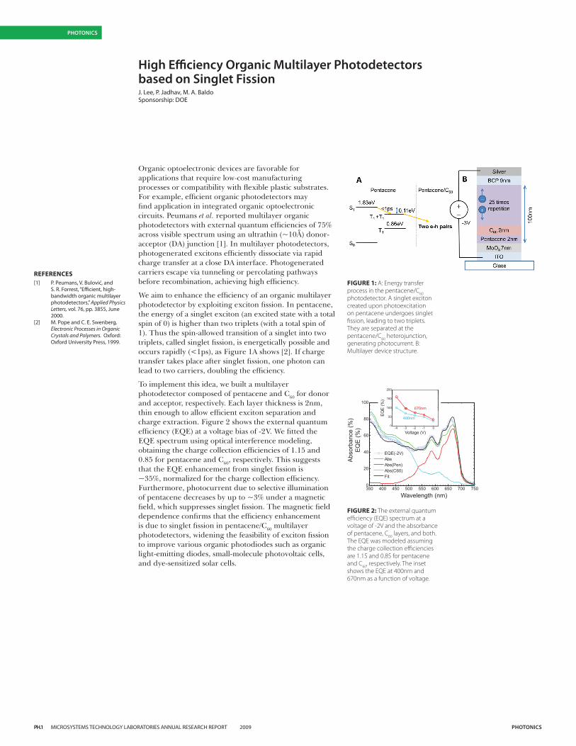
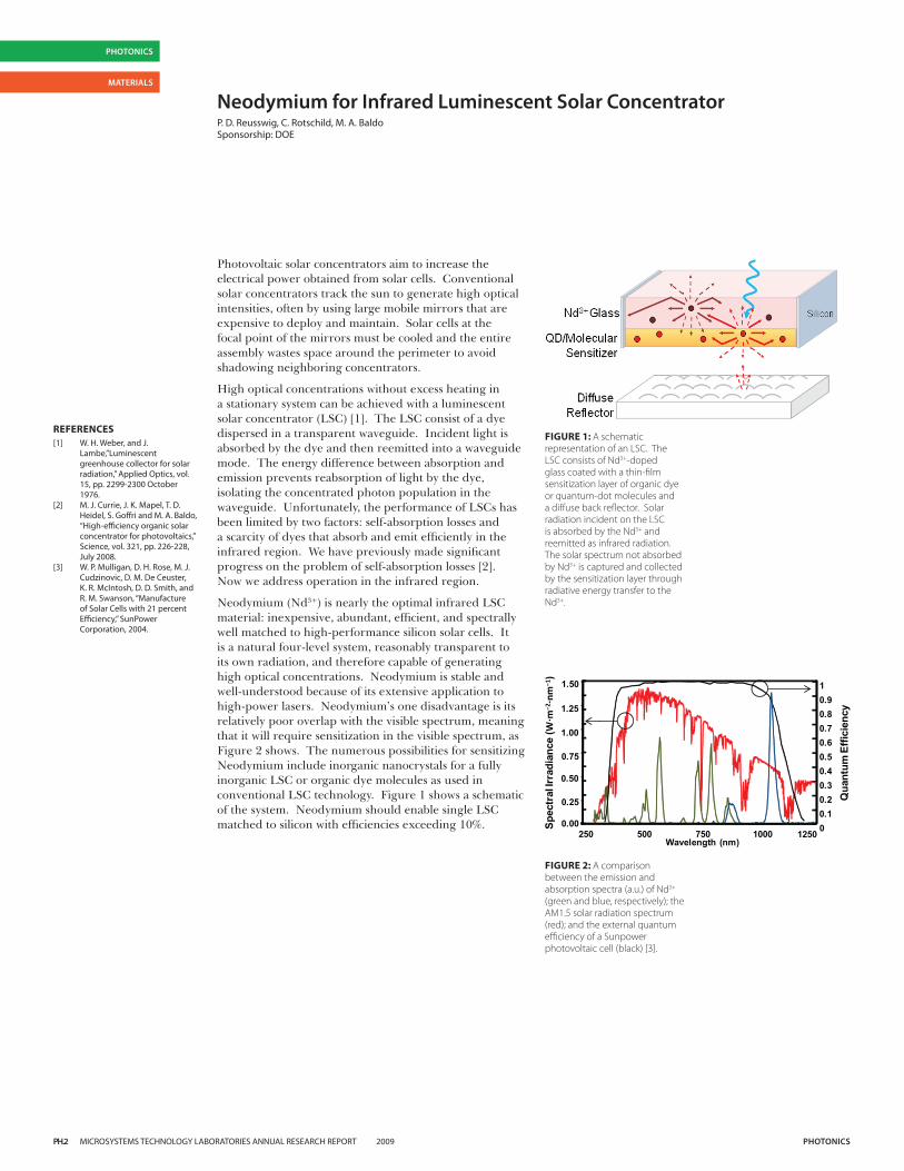
Neodymium (Nd3+) is nearly the optimal infrared LSC material: inexpensive, abundant, efficient, and spectrally well matched to high-performance silicon solar cells. It is a natural four-level system, reasonably transparent to its own radiation, and therefore capable of generating high optical concentrations. Neodymium is stable and well-understood because of its extensive application to high-power lasers. Neodymium’s one disadvantage is its relatively poor overlap with the visible spectrum, meaning that it will require sensitization in the visible spectrum, as Figure 2 shows. The numerous possibilities for sensitizing Neodymium include inorganic nanocrystals for a fully inorganic LSC or organic dye molecules as used in conventional LSC technology. Figure 1 shows a schematic of the system. Neodymium should enable single LSC matched to silicon with efficiencies exceeding 10%.
FIGURE 1: A schematic representation of an LSC. The LSC consists of Nd3+-doped glass coated with a thin-film sensitization layer of organic dye or quantum-dot molecules and a diffuse back reflector. Solar radiation incident on the LSC is absorbed by the Nd3+ and reemitted as infrared radiation. The solar spectrum not absorbed by Nd3+ is captured and collected by the sensitization layer through radiative energy transfer to the Nd3+.
0
0.1
0.2
0.3
0.4
0.5
0.6
0.7
0.8
0.9
1
0.00
0.25
0.50
0.75
1.00
1.25
1.50
250 500 750 1000 1250Wavelength (nm)
Qu
antu
m E
ffic
ien
cy
Sp
ectr
al Ir
rad
ian
ce (
W·m
−2·n
m−1
)
FIGURE 2: A comparison between the emission and absorption spectra (a.u.) of Nd3+ (green and blue, respectively); the AM1.5 solar radiation spectrum (red); and the external quantum efficiency of a Sunpower photovoltaic cell (black) [3].
REFERENCES[1] W. H. Weber, and J.
Lambe,”Luminescent greenhouse collector for solar radiation,” Applied Optics, vol. 15, pp. 2299-2300 October 1976.
[2] M. J. Currie, J. K. Mapel, T. D. Heidel, S. Goffri and M. A. Baldo, “High-efficiency organic solar concentrator for photovoltaics,” Science, vol. 321, pp. 226-228, July 2008.
[3] W. P. Mulligan, D. H. Rose, M. J. Cudzinovic, D. M. De Ceuster, K. R. McIntosh, D. D. Smith, and R. M. Swanson, “Manufacture of Solar Cells with 21 percent Efficiency,” SunPower Corporation, 2004.
PH.3 MICROSYSTEMS TECHNOLOGY LABORATORIES ANNUAL RESEARCH REPORT 2009 PHotonics
PHotonics
MAtERiALs
Efficiently coupling Light to superconducting nanowire single-photon Detectors X. Hu, T. Zhong, F. Najafi, C. Herder, F. N. C. Wong, K. K. BerggrenSponsorship: IARPA
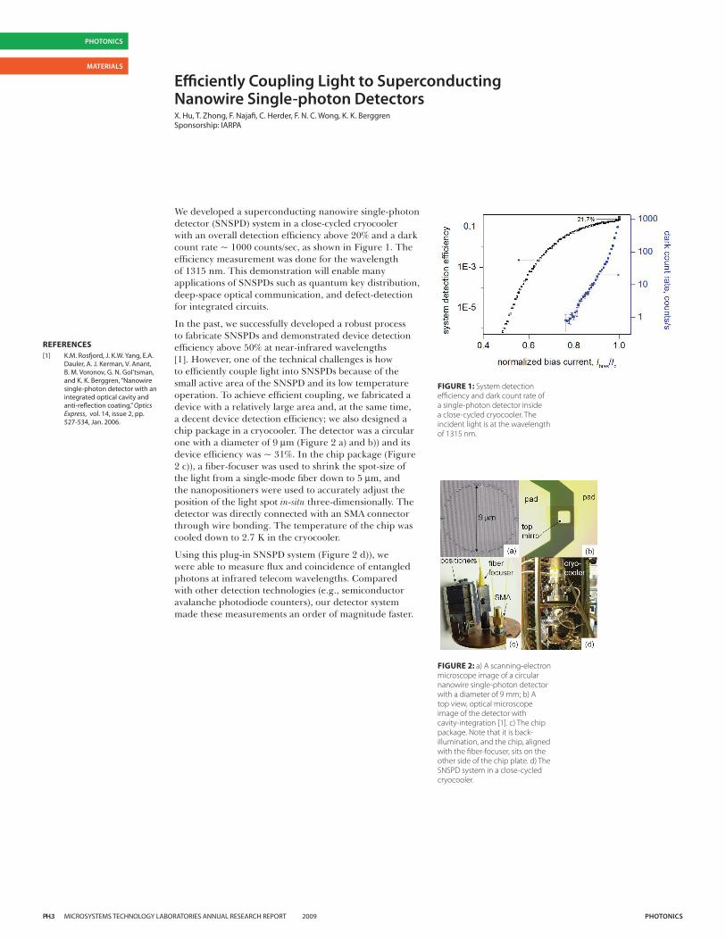
We developed a superconducting nanowire single-photon detector (SNSPD) system in a close-cycled cryocooler with an overall detection efficiency above 20% and a dark count rate ~ 1000 counts/sec, as shown in Figure 1. The efficiency measurement was done for the wavelength of 1315 nm. This demonstration will enable many applications of SNSPDs such as quantum key distribution, deep-space optical communication, and defect-detection for integrated circuits.
In the past, we successfully developed a robust process to fabricate SNSPDs and demonstrated device detection efficiency above 50% at near-infrared wavelengths [1]. However, one of the technical challenges is how to efficiently couple light into SNSPDs because of the small active area of the SNSPD and its low temperature operation. To achieve efficient coupling, we fabricated a device with a relatively large area and, at the same time, a decent device detection efficiency; we also designed a chip package in a cryocooler. The detector was a circular one with a diameter of 9 mm (Figure 2 a) and b)) and its device efficiency was ~ 31%. In the chip package (Figure 2 c)), a fiber-focuser was used to shrink the spot-size of the light from a single-mode fiber down to 5 mm, and the nanopositioners were used to accurately adjust the position of the light spot in-situ three-dimensionally. The detector was directly connected with an SMA connector through wire bonding. The temperature of the chip was cooled down to 2.7 K in the cryocooler.
Using this plug-in SNSPD system (Figure 2 d)), we were able to measure flux and coincidence of entangled photons at infrared telecom wavelengths. Compared with other detection technologies (e.g., semiconductor avalanche photodiode counters), our detector system made these measurements an order of magnitude faster.
FIGURE 1: System detection efficiency and dark count rate of a single-photon detector inside a close-cycled cryocooler. The incident light is at the wavelength of 1315 nm.
FIGURE 2: a) A scanning-electron microscope image of a circular nanowire single-photon detector with a diameter of 9 mm; b) A top view, optical microscope image of the detector with cavity-integration [1]. c) The chip package. Note that it is back-illumination, and the chip, aligned with the fiber-focuser, sits on the other side of the chip plate. d) The SNSPD system in a close-cycled cryocooler.
REFERENCES[1] K.M. Rosfjord, J. K.W. Yang, E.A.
Dauler, A. J. Kerman, V. Anant, B. M. Voronov, G. N. Gol’tsman, and K. K. Berggren, “Nanowire single-photon detector with an integrated optical cavity and anti-reflection coating,” Optics Express, vol. 14, issue 2, pp. 527-534, Jan. 2006.
PH.4 MICROSYSTEMS TECHNOLOGY LABORATORIES ANNUAL RESEARCH REPORT 2009 PHotonics
PHotonics
Guided-wave Devices for Holographic Video DisplayD. Smalley, V. M. Bove, Jr., Q. SmithwickSponsorship: CELab, Digital Life, and Things That Think Research Consortia and Center for Future Storytelling, MIT Media Laboratory
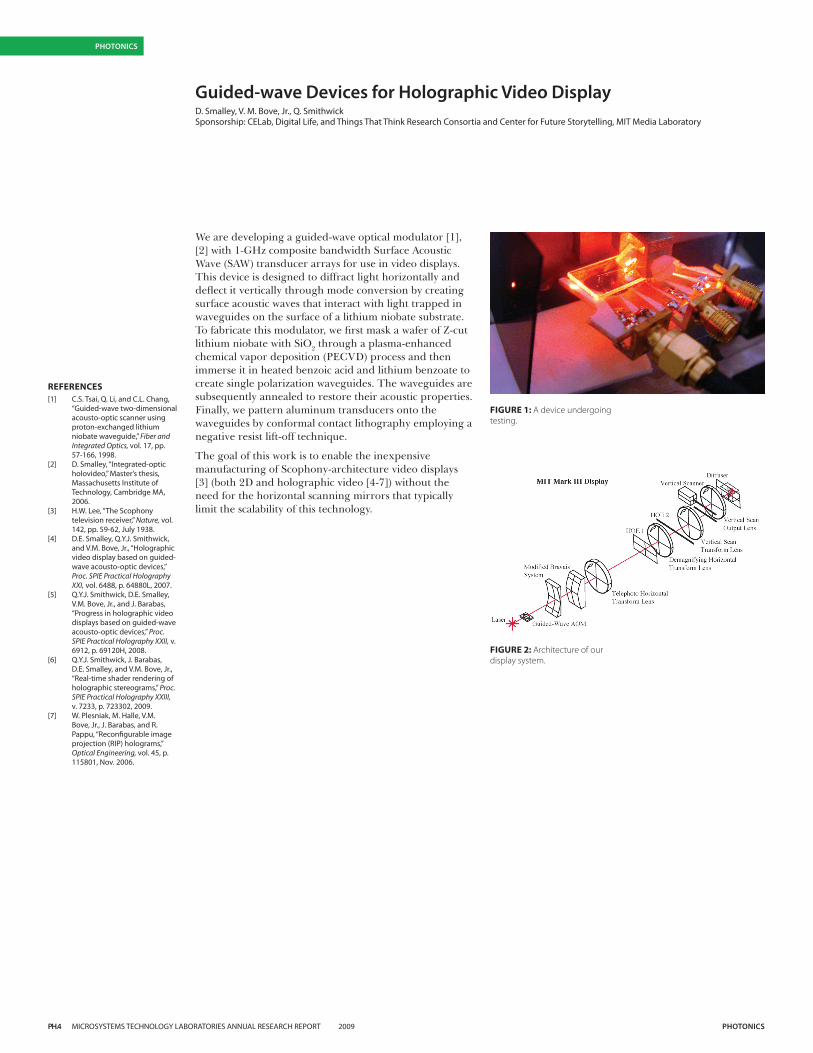
We are developing a guided-wave optical modulator [1], [2] with 1-GHz composite bandwidth Surface Acoustic Wave (SAW) transducer arrays for use in video displays. This device is designed to diffract light horizontally and deflect it vertically through mode conversion by creating surface acoustic waves that interact with light trapped in waveguides on the surface of a lithium niobate substrate. To fabricate this modulator, we first mask a wafer of Z-cut lithium niobate with SiO2 through a plasma-enhanced chemical vapor deposition (PECVD) process and then immerse it in heated benzoic acid and lithium benzoate to create single polarization waveguides. The waveguides are subsequently annealed to restore their acoustic properties. Finally, we pattern aluminum transducers onto the waveguides by conformal contact lithography employing a negative resist lift-off technique.
The goal of this work is to enable the inexpensive manufacturing of Scophony-architecture video displays [3] (both 2D and holographic video [4-7]) without the need for the horizontal scanning mirrors that typically limit the scalability of this technology.
FIGURE 1: A device undergoing testing.
FIGURE 2: Architecture of our display system.
REFERENCES[1] C.S. Tsai, Q. Li, and C.L. Chang,
“Guided-wave two-dimensional acousto-optic scanner using proton-exchanged lithium niobate waveguide,” Fiber and Integrated Optics, vol. 17, pp. 57-166, 1998.
[2] D. Smalley, “Integrated-optic holovideo,” Master’s thesis, Massachusetts Institute of Technology, Cambridge MA, 2006.
[3] H.W. Lee, “The Scophony television receiver,” Nature, vol. 142, pp. 59-62, July 1938.
[4] D.E. Smalley, Q.Y.J. Smithwick, and V.M. Bove, Jr., “Holographic video display based on guided-wave acousto-optic devices,” Proc. SPIE Practical Holography XXI, vol. 6488, p. 64880L, 2007.
[5] Q.Y.J. Smithwick, D.E. Smalley, V.M. Bove, Jr., and J. Barabas, “Progress in holographic video displays based on guided-wave acousto-optic devices,” Proc. SPIE Practical Holography XXII, v. 6912, p. 69120H, 2008.
[6] Q.Y.J. Smithwick, J. Barabas, D.E. Smalley, and V.M. Bove, Jr., “Real-time shader rendering of holographic stereograms,” Proc. SPIE Practical Holography XXIII, v. 7233, p. 723302, 2009.
[7] W. Plesniak, M. Halle, V.M. Bove, Jr., J. Barabas, and R. Pappu, “Reconfigurable image projection (RIP) holograms,” Optical Engineering, vol. 45, p. 115801, Nov. 2006.
PH.5 MICROSYSTEMS TECHNOLOGY LABORATORIES ANNUAL RESEARCH REPORT 2009 PHotonics
PHotonics
nAnotEcHnoLoGY
Exciton-exciton Annihilation in organic Polariton MicrocavitiesG. M. Akselrod, J. R. Tischler, E. R. Young, M. S. Bradley, D. G. Nocera, V. BulovićSponsorship: CMSE, RLE, Hertz Foundation
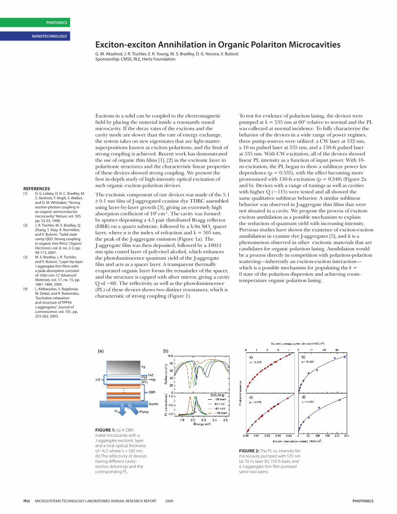
Excitons in a solid can be coupled to the electromagnetic field by placing the material inside a resonantly tuned microcavity. If the decay rates of the excitons and the cavity mode are slower than the rate of energy exchange, the system takes on new eigenstates that are light-matter superpositions known as exciton-polaritons, and the limit of strong coupling is achieved. Recent work has demonstrated the use of organic thin films [1], [2] as the excitonic layer in polaritonic structures and the characteristic linear properties of these devices showed strong coupling. We present the first in-depth study of high-intensity optical excitation of such organic exciton-polariton devices.
The excitonic component of our devices was made of the 5.1 ± 0.1 nm film of J-aggregated cyanine dye TDBC assembled using layer-by-layer growth [3], giving an extremely high absorption coefficient of 106 cm-1. The cavity was formed by sputter-depositing a 4.5 pair distributed Bragg reflector (DBR) on a quartz substrate, followed by a λ/4n SiO2 spacer layer, where n is the index of refraction and λ = 595 nm, the peak of the J-aggregate emission (Figure 1a). The J-aggregate film was then deposited, followed by a 100±1 nm spin coated layer of polyvinyl alcohol, which enhances the photoluminscence quantum yield of the J-aggregate film and acts as a spacer layer. A transparent thermally evaporated organic layer forms the remainder of the spacer, and the structure is capped with silver mirror, giving a cavity Q of ~60. The reflectivity as well as the photoluminscence (PL) of these devices shows two distinct resonances, which is characteristic of strong coupling (Figure 1).
To test for evidence of polariton lasing, the devices were pumped at λ = 535 nm at 60° relative to normal and the PL was collected at normal incidence. To fully characterize the behavior of the devices in a wide range of power regimes, three pump sources were utilized: a CW laser at 532 nm, a 10-ns pulsed laser at 535 nm, and a 150-fs pulsed laser at 535 nm. With CW excitation, all of the devices showed linear PL intensity as a function of input power. With 10-ns excitation, the PL began to show a sublinear power law dependence (p = 0.535), with the effect becoming more pronounced with 150-fs excitation (p = 0.348) (Figure 2a and b). Devices with a range of tunings as well as cavities with higher Q (~115) were tested and all showed the same qualitative sublinear behavior. A similar sublinear behavior was observed in J-aggregate thin films that were not situated in a cavity. We propose the process of exciton-exciton annhilation as a possible mechanism to explain the reduction of quantum yield with increasing intensity. Previous studies have shown the existence of exciton-exciton annihilation in cyanine dye J-aggregates [5], and it is a phenomenon observed in other excitonic materials that are candidates for organic polariton lasing. Annihilation would be a process directly in competition with polariton-polariton scattering—inherently an exciton-exciton interaction—which is a possible mechanism for populating the k = 0 state of the polariton dispersion and achieving room- temperature organic polariton lasing.
REFERENCES[1] D. G. Lidzey, D. D. C. Bradley, M.
S. Skolnick, T. Virgili, S. Walker, and D. M. Whittaker, “Strong exciton-photon coupling in an organic semiconductor microcavity,” Nature, vol. 395 pp. 53-55, 1998.
[2] J. R. Tischler, M. S. Bradley, Q. Zhang, T. Atay, A. Nurmikko, and V. Bulović, “Solid state cavity QED: Strong coupling in organic thin films,” Organic Electronics vol. 8, no. 2-3, pp. 94-113, 2007.
[3] M. S. Bradley, J. R. Tischler, and V. Bulović, “Layer-by-layer J-aggregate thin films with a peak absorption constant of 10(6) cm(-1),” Advanced Materials, vol. 17, no. 15, pp. 1881-1884, 2005.
[4] L. Kelbauskas, S. Bagdonas, W. Dietel, and R. Rotomskis, “Excitation relaxation and structure of TPPS4 J-aggregates,” Journal of Luminescence, vol. 101, pp. 253-262, 2003.
FIGURE 1: (a) A DBR-metal microcavity with a J-aggregate excitonic layer and a total optical thickness of ~λ/2 where λ = 595 nm. (b) The reflectivity of devices having different cavity-exciton detunings and the corresponding PL.
FIGURE 2: The PL vs. intensity for: microcavity pumped with 535 nm (a) 10 ns laser (b) 150 fs laser; and a J-aggregate thin film pumped same two lasers.
PH.6 MICROSYSTEMS TECHNOLOGY LABORATORIES ANNUAL RESEARCH REPORT 2009 PHotonics
PHotonics
nAnotEcHnoLoGY
Heterojunction Photovoltaics Using Printed colloidal Quantum Dots as the Photosensitive LayerA. C. Arango, S. Geyer, M. G. Bawendi, V. BulovićSponsorship: ISN, DOE Solar America Program
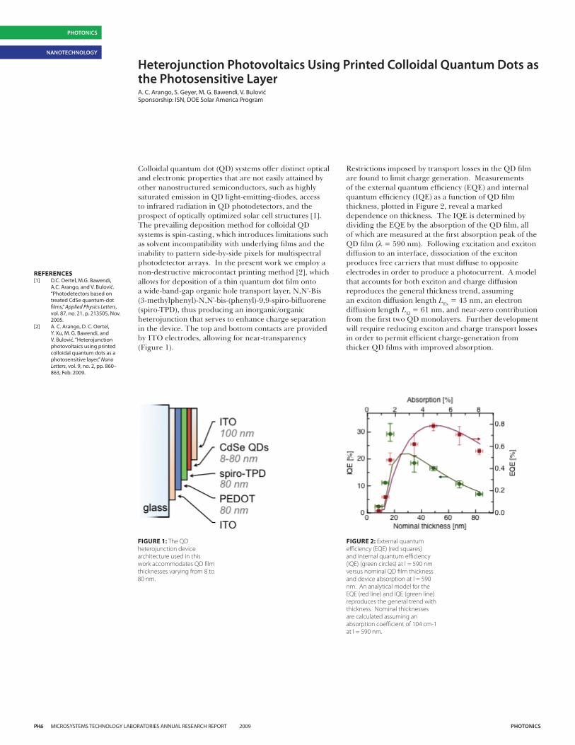
Colloidal quantum dot (QD) systems offer distinct optical and electronic properties that are not easily attained by other nanostructured semiconductors, such as highly saturated emission in QD light-emitting-diodes, access to infrared radiation in QD photodetectors, and the prospect of optically optimized solar cell structures [1]. The prevailing deposition method for colloidal QD systems is spin-casting, which introduces limitations such as solvent incompatibility with underlying films and the inability to pattern side-by-side pixels for multispectral photodetector arrays. In the present work we employ a non-destructive microcontact printing method [2], which allows for deposition of a thin quantum dot film onto a wide-band-gap organic hole transport layer, N,N'-Bis (3-methylphenyl)-N,N'-bis-(phenyl)-9,9-spiro-bifluorene (spiro-TPD), thus producing an inorganic/organic heterojunction that serves to enhance charge separation in the device. The top and bottom contacts are provided by ITO electrodes, allowing for near-transparency (Figure 1).
Restrictions imposed by transport losses in the QD film are found to limit charge generation. Measurements of the external quantum efficiency (EQE) and internal quantum efficiency (IQE) as a function of QD film thickness, plotted in Figure 2, reveal a marked dependence on thickness. The IQE is determined by dividing the EQE by the absorption of the QD film, all of which are measured at the first absorption peak of the QD film (λ = 590 nm). Following excitation and exciton diffusion to an interface, dissociation of the exciton produces free carriers that must diffuse to opposite electrodes in order to produce a photocurrent. A model that accounts for both exciton and charge diffusion reproduces the general thickness trend, assuming an exciton diffusion length LEx = 43 nm, an electron diffusion length LEl = 61 nm, and near-zero contribution from the first two QD monolayers. Further development will require reducing exciton and charge transport losses in order to permit efficient charge-generation from thicker QD films with improved absorption.
REFERENCES[1] D.C. Oertel, M.G. Bawendi,
A.C. Arango, and V. Bulović. “Photodetectors based on treated CdSe quantum-dot films,” Applied Physics Letters, vol. 87, no. 21, p. 213505, Nov. 2005.
[2] A. C. Arango, D. C. Oertel, Y. Xu, M. G. Bawendi, and V. Bulović. “Heterojunction photovoltaics using printed colloidal quantum dots as a photosensitive layer,” Nano Letters, vol. 9, no. 2, pp. 860–863, Feb. 2009.
FIGURE 1: The QD heterojunction device architecture used in this work accommodates QD film thicknesses varying from 8 to 80 nm.
FIGURE 2: External quantum efficiency (EQE) (red squares) and internal quantum efficiency (IQE) (green circles) at l = 590 nm versus nominal QD film thickness and device absorption at l = 590 nm. An analytical model for the EQE (red line) and IQE (green line) reproduces the general trend with thickness. Nominal thicknesses are calculated assuming an absorption coefficient of 104 cm-1 at l = 590 nm.
PH.7 MICROSYSTEMS TECHNOLOGY LABORATORIES ANNUAL RESEARCH REPORT 2009 PHotonics
PHotonics
nAnotEcHnoLoGY
Patterned organic Microcavities for confinement of Exciton-PolaritonsM. S. Bradley, J. R. Tischler, G. Akselrod, V. BulovićSponsorship: NDSEG, ISN
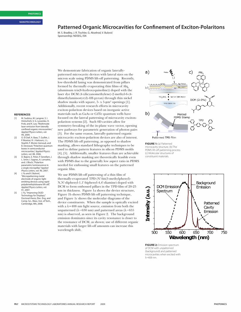
We demonstrate fabrication of organic laterally-patterned microcavity devices with lateral sizes on the micron scale using PDMS lift-off patterning. Recently, low-threshold lasing was demonstrated from pillars formed by thermally evaporating thin films of Alq3 (aluminum tris(8-hydroxyquinoline)) doped with the laser dye DCM (4-(dicyanomethylene)-2-methyl-6-(4-dimethylaminostyryl)-4H-pyran) through thin nickel shadow masks with square, 5- x 5-mm2 openings [1]. Additionally, recent research efforts in microcavity exciton-polariton devices based on inorganic active materials such as GaAs or CdTe quantum wells have focused on the lateral patterning of microcavity exciton-polariton systems [2]. Such 0D cavities allow for symmetry-breaking of the in-plane wave vector, opening new pathways for parametric generation of photon pairs [3]. For the same reason, laterally-patterned organic microcavity exciton-polariton devices are also of interest. The PDMS lift-off patterning, as opposed to shadow masking, allows standard lithography techniques to be used to define pattern features in silicon PDMS molds [4], [5]. Additionally, smaller features than are achievable through shadow masking are theoretically feasible even with PDMS due to the generally low aspect ratio in PDMS needed for embossing small features on the patterned organic film.
We use PDMS lift-off patterning of a thin film of thermally-evaporated TPD (N'-bis(3-methylphenyl)-N,N'-diphenyl-1,1'-biphenyl-4,4'-diamine) doped with DCM to form embossed pillars in the TPD film of 20-25 nm in thickness. Figure 1a shows the device structure, Figure 1b shows PDMS lift-off patterning technique, and Figure 1c shows the molecular diagrams of the device constituents. When the sample is optically excited with a λ=408 nm light source, emission from both the unpatterned (λ~630 nm) and patterned areas (λ~655 nm) is observed, as seen in Figure 2. The background emission dominates since its cavity resonance is closer to the resonance of DCM, as shown; use of different organic materials with larger lift-off amounts can increase this wavelength shift.
FIGURE 1: (a) Patterned microcavity structure. (b) The PDMS lift-off patterning process. (c) Molecular structures of constituent materials.
FIGURE 2: Emission spectrum of DCM with unpatterned (background) and patterned microcavities when excited with λ=408 nm.
REFERENCES[1] M. Sudzius, M. Langner, S. I.
Hintschich, V. G. Lyssenko, H. Frob, and K. Leo, “Multimode laser emission from laterally confined organic microcavities,” Applied Physics Letters, vol. 94, 2009.
[2] O. El Daif, A. Baas, T. Guillet, J. P. Brantut, R. I. Kaitouni, J. L. Staehli, F. Morier-Genoud, and B. Deveaud, “Polariton quantum boxes in semiconductor microcavities,” Applied Physics Letters, vol. 88, 2006.
[3] D. Bajoni, E. Peter, P. Senellart, J. L. Smirr, I. Sagnes, A. Lemaitre, and J. Bloch, “Polariton parametric luminescence in a single micropillar,” Applied Physics Letters, vol. 90, 2007.
[4] J. Yu and V. Bulović, “Micropatterning metal electrode of organic light emitting devices using rapid polydimethylsiloxane lift-off,” Applied Physics Letters, vol. 91, 2007.
[5] J. Yu, “Improving OLED Technology for Displays,” Doctoral thesis, Elec. Eng. and Comp. Sci., Mass. Inst. of Tech., Cambridge, MA, 2008.
PH.8 MICROSYSTEMS TECHNOLOGY LABORATORIES ANNUAL RESEARCH REPORT 2009 PHotonics
PHotonics
nAnotEcHnoLoGY
Heterojunction Photodetector consisting of Metal-oxide and colloidal Quantum-dot thin FilmsT. P. Osedach, N. Zhao, L.-Y. Chang, S. M. Geyer, A. C. Arango, J. C. Ho, M. Bawendi, V. BulovićSponsorship: ISN, DOE Solar America Program
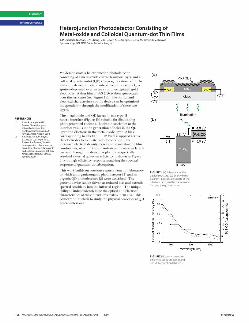
We demonstrate a heterojunction photodetector consisting of a metal-oxide charge transport layer and a colloidal quantum-dot (QD) charge-generation layer. To make the device, a metal-oxide semiconductor, SnO2, is sputter-deposited over an array of interdigitated gold electrodes. A thin film of PbS QDs is then spin-coated over the structure (see Figure 1a). The optical and electrical characteristics of the device can be optimized independently through the modification of these two layers.
The metal-oxide and QD layers form a type-II hetero-interface (Figure 1b) suitable for dissociating photogenerated excitons. Exciton dissociation at the interface results in the generation of holes in the QD layer and electrons in the metal-oxide layer. A bias corresponding to a field of ~104 V/cm is applied across the electrodes to facilitate carrier collection. The increased electron density increases the metal-oxide film conductivity, which in turn manifests an increase in lateral current through the device. A plot of the spectrally resolved external quantum efficiency is shown in Figure 2, with high efficiency response matching the spectral response of quantum-dot absorption.
This work builds on previous reports from our laboratory in which an organic/organic photodetector [1] and an organic/QD photodetector [2] were described. The present device can be driven at reduced bias and extends spectral sensitivity into the infrared region. The unique ability to independently tune the optical and electrical characteristics of these structures makes them a valuable platform with which to study the physical processes at QD hetero-interfaces.
FIGURE 1: (a) Schematic of the device structure. (b) Energy band diagram. Excitons dissociate at the interface between the metal-oxide film and the quantum dots.
FIGURE 2: External quantum efficiency spectrum (solid) and PbS QD absorption (dashed).
REFERENCES[1] J. Ho, A. Arango, and V.
Bulović, “Lateral organic bilayer heterojunction photoconductors”, Applied Physics Letters, August 2008.
[2] T. P. Osedach, S. M. Geyer, J. C. Ho, A. C. Arango, M. G. Bawendi, V. Bulović, “Lateral heterojunction photodetector consisting of molecular organic and colloidal quantum dot thin films”, Applied Physics Letters, January 2009.
PH.9 MICROSYSTEMS TECHNOLOGY LABORATORIES ANNUAL RESEARCH REPORT 2009 PHotonics
PHotonics
MAtERiALs
Heterojunction Photoconductors for chemical DetectionJ. C. Ho, J. A. Rowehl, V. BulovićSponsorship: ISN, CMSE
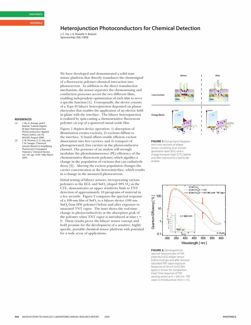
We have developed and demonstrated a solid-state sensor platform that directly transduces the chemosignal of a fluorescent polymer-chemical interaction into photocurrent. In addition to the direct transduction mechanism, the sensor separates the chemosensing and conduction processes across the two different films, enabling independent optimization of each film to serve a specific function [1]. Conceptually, the device consists of a Type-II bilayer heterojunction deposited on planar electrodes that enables the application of an electric field in-plane with the interface. The bilayer heterojunction is realized by spin-casting a chemosensitive fluorescent polymer on top of a sputtered metal oxide film.
Figure 1 depicts device operation: 1) absorption of illumination creates excitons, 2) excitons diffuse to the interface, 3) band offsets enable efficient exciton dissociation into free carriers, and 4) transport of photogenerated, free carriers in the photoconductive channel. The presence of an analyte will strongly modulate the photoluminescence (PL) efficiency of the chemosensitive fluorescent polymer, which signifies a change in the population of excitons that can radiatively decay [2] . Altering the exciton population changes the carrier concentration at the heterointerface, which results in a change in the measured photocurrent.
Initial testing of bilayer sensors, incorporating various polymers as the EGL and SnO2 (doped 30% O2) as the CTL, demonstrates an upper sensitivity limit to TNT detection of approximately 10 picograms of material in a few seconds. Figure 2 compares the spectral response of a 100-nm film of SnO2 to a bilayer device (100 nm SnO2/5nm HW polymer) before and after exposure to saturated TNT vapor. The inset shows the real-time change in photoconductivity at the absorption peak of the polymer when TNT vapor is introduced at time t = 0. These results prove the bilayer sensor concept and hold promise for the development of a sensitive, highly specific, portable chemical sensor platform with potential for a wide array of applications.
FIGURE 1: Energy band diagrams and cross-sections of bilayer sensor consisting of an exciton generation layer (EGL) and a charge transport layer (CTL) before and after exposure to a particular analyte.
FIGURE 2: Semilogarithmic spectral response plot of HW polymer/SnO2 bilayer sensor before (orange) and after (brown) saturated TNT vapor exposure. Response of 20-nm SnO2 film (grey) is shown for comparison. Inset: Time response of TNT sensing action at ë = 500 nm. TNT vapor is introduced at time t = 0 s.
REFERENCES[1] J. Ho, A. Arango, and V.
Bulović, “Lateral Organic Bi-layer Heterojunction Photoconductors,” Applied Physics Letters, vol. 93, 063305, August 2008.
[2] S. W. Thomas, G. D. Joly, and T. M. Swager, “Chemical Sensors Based on Amplifying Fluorescent Conjugated Polymers,” Chemical Review, vol. 107, pp. 1339-1386, March 2007.
PH.10 MICROSYSTEMS TECHNOLOGY LABORATORIES ANNUAL RESEARCH REPORT 2009 PHotonics
PHotonics
nAnotEcHnoLoGY
Multi-layer Heterojunction PhotoconductorsJ. C. Ho, J. A. Rowehl, V. BulovićSponsorship: ISN, CMSE
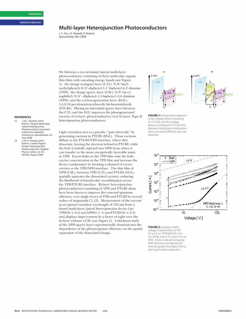
We fabricate a two-terminal, lateral multi-layer photoconductor consisting of three molecular organic thin films with cascading energy bands (see Figure 1): the charge transport layer (CTL), N,N’-bis(3-methylphenyl)-N,N’-diphenyl-1,1’-biphenyl-4,4’-diamine (TPD); the charge spacer layer (CSL), N,N’-bis-(1-naphthyl)-N,N’ –diphenyl-1,1-bipheny1-4,4’-diamine (NPD); and the exciton-generation layer (EGL), 3,4,9,10-perylenetetracarboxylic bis-benzimidazole (PTCBI). Placing an interstitial spacer layer between the CTL and the EGL improves the photogenerated current of tri-layer photoconductors over bi-layer, Type-II heterojunction photoconductors.
Light excitation acts as a pseudo- “gate electrode” by generating excitons in PTCBI (EGL). Those excitons diffuse to the PTCBI/NPD interface, where they dissociate, leaving the electron behind in PTCBI, while the hole is initially injected into NPD from where it can transfer to the more energetically favorable states in TPD. Excess holes in the TPD film raise the hole-carrier concentration in the TPD film and increase the device conductance by forming a channel of excess carriers at the TPD/NPD interface. The thin film of NPD (CSL), between TPD (CTL) and PTCBI (EGL), spatially separates the dissociated carriers, reducing the likelihood of bimolecular recombination across the TPD/PTCBI interface. Bi-layer heterojunction photoconductors consisting of TPD and PTCBI alone have been shown to improve the external quantum efficiency over single layers of TPD and PTCBI by several orders of magnitude [1], [2]. Measurement of the current at an optical excitation wavelength of 532 nm from a biased multi-layer, lateral heterojunction device [Au/TPD(50 ± 0.5) nm/NPD(4 ± 1) nm/PTCBI(50 ± 0.5) nm] displays improvement by a factor of eight over the bi-layer without a CSL (see Figure 2). A thickness study of the NPD spacer layer experimentally demonstrates the dependence of the photoresponse efficiency on the spatial separation of the dissociated charge.
FIGURE 1: Energy-band diagrams of (a) a bilayer device consisting of CTL/EGL and (b) a trilayer device consisting of CTL/CSL/EGL. Relevant interfacial recombination rates and carrier diffusion rates are depicted.
FIGURE 2: Log-log current-voltage characteristics of TPD 50 ± 0.5 nm TPD/NPD/50 ± 0.5 nm PTCBI, with 0, 3.5, and 4 nm of NPD. Arrows indicate increasing NPD thickness and dashed red lines are guides that depict ohmic and trap-limited conduction.
REFERENCES[1] J. Ho, J. Rowehl, and V.
Bulović, “Organic Multi-layer Lateral Heterojunction Phototransistors,” presented at Electronic Materials Conference, Santa Barbara, CA, June 2008.
[2] J. Ho, A. Arango, and V. Bulović, “Lateral Organic Bi-layer Heterojunction Photoconductors,” Applied Physics Letters, vol. 93, 063305, August 2008.
PH.11 MICROSYSTEMS TECHNOLOGY LABORATORIES ANNUAL RESEARCH REPORT 2009 PHotonics
PHotonics
nAnotEcHnoLoGY
3-molecular-layers-thick J-aggregate PhotoconductorY. Shirasaki, J. Ho, M. S. Bradley, J. R. Tischler, V. BulovićSponsorship: ISN, Solar Revolutions Center at MIT, NSF MRSEC
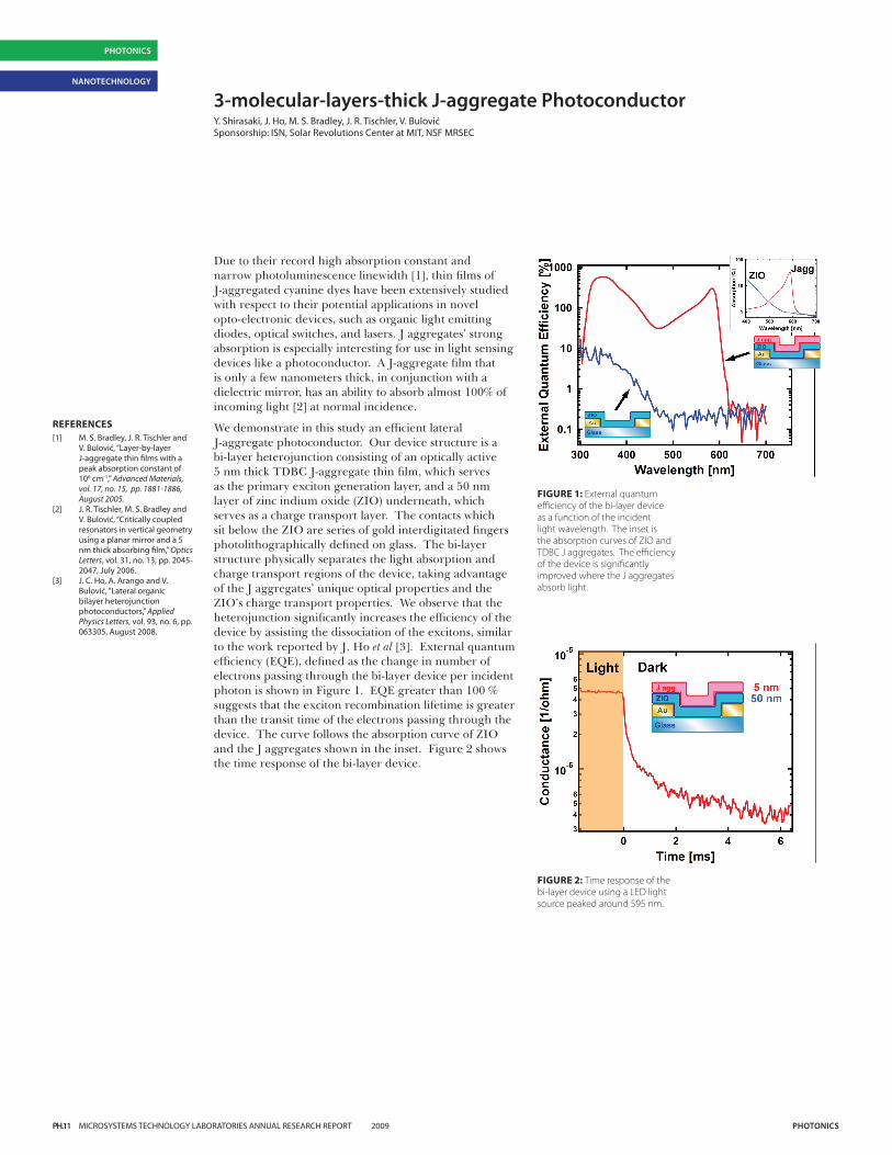
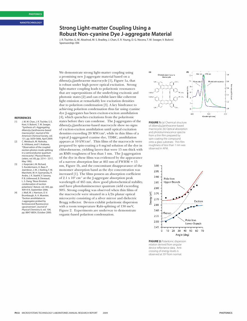
Due to their record high absorption constant and narrow photoluminescence linewidth [1], thin films of J-aggregated cyanine dyes have been extensively studied with respect to their potential applications in novel opto-electronic devices, such as organic light emitting diodes, optical switches, and lasers. J aggregates’ strong absorption is especially interesting for use in light sensing devices like a photoconductor. A J-aggregate film that is only a few nanometers thick, in conjunction with a dielectric mirror, has an ability to absorb almost 100% of incoming light [2] at normal incidence.
We demonstrate in this study an efficient lateral J-aggregate photoconductor. Our device structure is a bi-layer heterojunction consisting of an optically active 5 nm thick TDBC J-aggregate thin film, which serves as the primary exciton generation layer, and a 50 nm layer of zinc indium oxide (ZIO) underneath, which serves as a charge transport layer. The contacts which sit below the ZIO are series of gold interdigitated fingers photolithographically defined on glass. The bi-layer structure physically separates the light absorption and charge transport regions of the device, taking advantage of the J aggregates’ unique optical properties and the ZIO’s charge transport properties. We observe that the heterojunction significantly increases the efficiency of the device by assisting the dissociation of the excitons, similar to the work reported by J. Ho et al [3]. External quantum efficiency (EQE), defined as the change in number of electrons passing through the bi-layer device per incident photon is shown in Figure 1. EQE greater than 100 % suggests that the exciton recombination lifetime is greater than the transit time of the electrons passing through the device. The curve follows the absorption curve of ZIO and the J aggregates shown in the inset. Figure 2 shows the time response of the bi-layer device.
FIGURE 1: External quantum efficiency of the bi-layer device as a function of the incident light wavelength. The inset is the absorption curves of ZIO and TDBC J aggregates. The efficiency of the device is significantly improved where the J aggregates absorb light.
FIGURE 2: Time response of the bi-layer device using a LED light source peaked around 595 nm.
REFERENCES[1] M. S. Bradley, J. R. Tischler and
V. Bulović, “Layer-by-layer J-aggregate thin films with a peak absorption constant of 106 cm-1,” Advanced Materials, vol. 17, no. 15, pp. 1881-1886, August 2005.
[2] J. R. Tischler, M. S. Bradley and V. Bulović, “Critically coupled resonators in vertical geometry using a planar mirror and a 5 nm thick absorbing film,” Optics Letters, vol. 31, no. 13, pp. 2045-2047, July 2006.
[3] J. C. Ho, A. Arango and V. Bulović, “Lateral organic bilayer heterojunction photoconductors,” Applied Physics Letters, vol. 93, no. 6, pp. 063305, August 2008.
PH.12 MICROSYSTEMS TECHNOLOGY LABORATORIES ANNUAL RESEARCH REPORT 2009 PHotonics
PHotonics
nAnotEcHnoLoGY
strong Light-matter coupling Using a Robust non-cyanine Dye J-aggregate MaterialJ. R. Tischler, G. M. Akselrod, M. S. Bradley, J. Chan, E. R. Young, D. G. Nocera, T. M. Swager, V. BulovićSponsorship: ISN
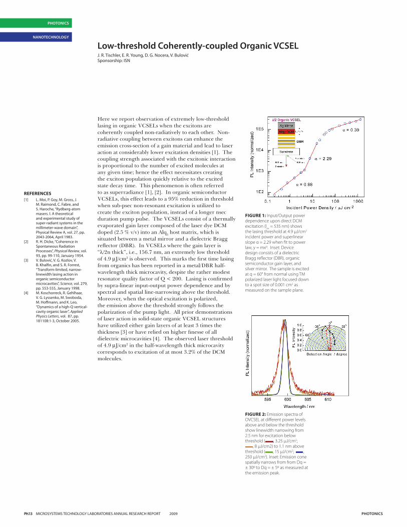
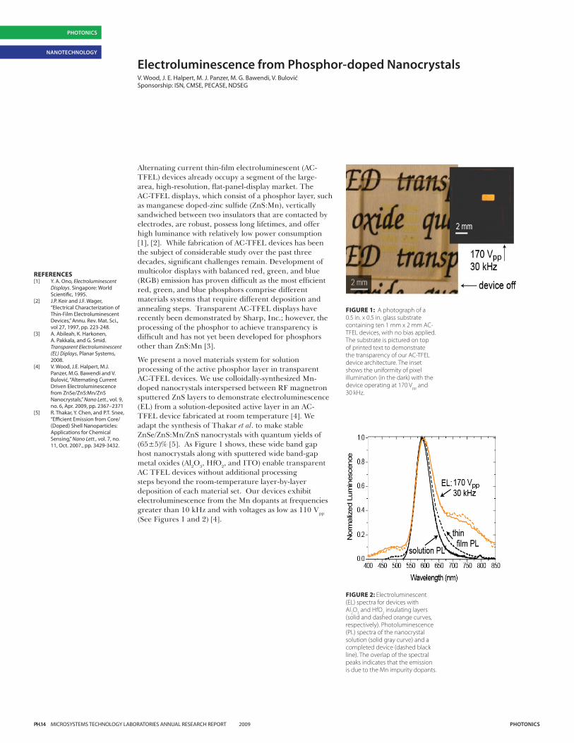
We demonstrate strong light-matter coupling using a promising new J-aggregate material based on a dibenz[a,j]anthracene macrocycle [1], Figure 1a, that is robust under high power optical excitation. Strong light-matter coupling leads to polaritonic resonances that are superpositions of the underlying excitonic and photonic states [2] and can exhibit laser-like coherent light emission at remarkably low excitation densities due to polariton condensation [3]. A key hindrance to achieving polariton condensation thus far using cyanine dye J-aggregates has been exciton-exciton annihilation [4], which quenches excitations from the polaritonic states before they can condense. The J-aggregates of the dibenz[a,j]anthracene-based macrocycle show no signs of exciton-exciton annihilation until optical excitation densities exceeding 20 MW/cm2, while in thin films of a typical J-aggregated cyanine dye, TDBC, annihilation appears at 10 kW/cm2. Thin films of the macrocycle were prepared by spin-coating a 6 mg/ml solution of the dye in chlorobenzene, yielding layers that were 15 nm thick with an RMS roughness of less than 1 nm. The J-aggregation of the dye in these films was evidenced by the appearance of a narrow absorption line at 465 nm of FWHM = 15 nm, Figure 1b, and the concomitant disappearance of the monomer absorption band as the dye concentration was increased [1]. The films possess an absorption coefficient of 2.1 x 105 cm-1 at the J-aggregate absorption peak wavelength of 465 nm, show good photochemical stability, and have photoluminescence quantum yield exceeding 90%. Strong coupling was observed when thin films of the macrocycle were situated in a λ/2n planar optical microcavity consisting of a silver mirror and dielectric Bragg reflector. Devices exhibit polaritonic dispersion with a room temperature Rabi-splitting of 130 meV, Figure 2. Experiments are underway to demonstrate organic-based polariton condensation.
REFERENCES[1] J. M. W. Chan, J. R. Tischler, S. E.
Kooi, V. Bulović, T. M. Swager, “Synthesis of J-Aggregating dibenz[a,J]anthracene-based macrocycles”, Journal of the American Chemical Society, vol. 131, pp. 5659-5666, April 2009.
[2] C. Weisbuch, M. Nishioka, A. Ishikawa, and Y. Arakawa, “Observation of the coupled exciton-photon mode splitting in a semiconductor quantum microcavity”, Physical Review Letters, vol. 69, pp. 3314 – 3317, May 1992.
[3] J. Kasprzak J, M. Richard, S. Kundermann, A. Baas, P. Jeambrun, J. M. J. Keeling, F. M. Marchetti, M. H. Szymanska, R. Andre, J. K. Staehli, V. Savona, P. B. Littlewood, B. Deveaud, L. S. Dang, “Bose-Einstein condensation of exciton polaritons”, Nature, vol. 443, pp. 409-414, September 2006.
[4] J. Moll, W. J. Harrison, D. V. Brumbaugh, A. A. Muenter, “Exciton annihilation in J-aggregates probed by femtosecond fluorescence upconversion”, Journal of Physical Chemistry A, vol. 104, pp. 8847-8854, October 2000.
FIGURE 1: (a) Chemical structure of dibenz[a,j]anthracene-based macrocycle. (b) Optical absorption and photoluminescence spectra from a thin film prepared by spin-coating the compound onto a glass substrate. Thin film roughness of less than 1 nm was observed in AFM.
FIGURE 2: Polaritonic dispersion relation derived from angular device reflectance data. Anti-crossing of energy levels is observed at 35º from normal.
PH.13 MICROSYSTEMS TECHNOLOGY LABORATORIES ANNUAL RESEARCH REPORT 2009 PHotonics
PHotonics
nAnotEcHnoLoGY
Low-threshold coherently-coupled organic VcsELJ. R. Tischler, E. R. Young, D. G. Nocera, V. BulovićSponsorship: ISN
Here we report observation of extremely low-threshold lasing in organic VCSELs when the excitons are coherently coupled non-radiatively to each other. Non-radiative coupling between excitons can enhance the emission cross-section of a gain material and lead to laser action at considerably lower excitation densities [1]. The coupling strength associated with the excitonic interaction is proportional to the number of excited molecules at any given time; hence the effect necessitates creating the exciton population quickly relative to the excited state decay time. This phenomenon is often referred to as superradiance [1], [2]. In organic semiconductor VCSELs, this effect leads to a 95% reduction in threshold when sub-psec non-resonant excitation is utilized to create the exciton population, instead of a longer nsec duration pump pulse. The VCSELs consist of a thermally evaporated gain layer composed of the laser dye DCM doped (2.5 % v/v) into an Alq3 host matrix, which is situated between a metal mirror and a dielectric Bragg reflector (DBR). In VCSELs where the gain layer is “λ/2n thick”, i.e., 156.7 nm, an extremely low threshold of 4.9 mJ/cm2 is observed. This marks the first time lasing from organics has been reported in a metal/DBR half-wavelength thick microcavity, despite the rather modest resonator quality factor of Q < 200. Lasing is confirmed by supra-linear input-output power dependence and by spectral and spatial line-narrowing above the threshold. Moreover, when the optical excitation is polarized, the emission above the threshold strongly follows the polarization of the pump light. All prior demonstrations of laser action in solid-state organic VCSEL structures have utilized either gain layers of at least 3 times the thickness [3] or have relied on higher finesse of all dielectric microcavities [4]. The observed laser threshold of 4.9 mJ/cm2 in the half-wavelength thick microcavity corresponds to excitation of at most 3.2% of the DCM molecules.
FIGURE 1: Input/Output power dependence upon direct DCM excitation (lex = 535 nm) shows the lasing threshold at 4.9 μJ/cm2 incident power and superlinear slope α = 2.29 when fit to power law, y = mxα. Inset: Device design consists of a dielectric Bragg reflector (DBR), organic semiconductor gain layer, and silver mirror. The sample is excited at q = 60° from normal using TM polarized laser light focused down to a spot size of 0.001 cm2 as measured on the sample plane.
FIGURE 2: Emission spectra of OVCSEL at different power levels above and below the threshold show linewidth narrowing from 2.5 nm for excitation below threshold ( , 3.25 μJ/cm2;
, 8 μJ/cm2) to 1.1 nm above threshold ( , 15 μJ/cm2; , 250 μJ/cm2). Inset: Emission cone spatially narrows from from Dq = ± 30º to Dq = ± 5º as measured at the emission peak.
REFERENCES[1] L. Moi, P. Goy, M. Gross, J.
M. Raimond, C. Fabre, and S. Haroche, “Rydberg-atom masers. I. A theoretical and experimental study of super-radiant systems in the millimeter-wave domain”, Physical Review A, vol. 27, pp. 2043-2064, April 1983.
[2] R. H. Dicke, “Coherence in Spontaneous Radiation Processes”, Physical Review, vol. 93, pp. 99-110, January 1954.
[3] V. Bulović, V. G. Kozlov, V. B. Khalfin, and S. R. Forrest, “Transform-limited, narrow-linewidth lasing action in organic semiconductor microcavities”, Science, vol. 279, pp. 553-555, January 1998.
[4] M. Koschorreck, R. Gehlhaar, V. G. Lyssenko, M. Swoboda, M. Hoffmann, and K. Leo, “Dynamics of a high-Q vertical-cavity organic laser”, Applied Physics Letters, vol. 87, pp. 181108:1-3, October 2005.
PH.14 MICROSYSTEMS TECHNOLOGY LABORATORIES ANNUAL RESEARCH REPORT 2009 PHotonics
PHotonics
nAnotEcHnoLoGY
Electroluminescence from Phosphor-doped nanocrystalsV. Wood, J. E. Halpert, M. J. Panzer, M. G. Bawendi, V. BulovićSponsorship: ISN, CMSE, PECASE, NDSEG
Alternating current thin-film electroluminescent (AC-TFEL) devices already occupy a segment of the large-area, high-resolution, flat-panel-display market. The AC-TFEL displays, which consist of a phosphor layer, such as manganese doped-zinc sulfide (ZnS:Mn), vertically sandwiched between two insulators that are contacted by electrodes, are robust, possess long lifetimes, and offer high luminance with relatively low power consumption [1], [2]. While fabrication of AC-TFEL devices has been the subject of considerable study over the past three decades, significant challenges remain. Development of multicolor displays with balanced red, green, and blue (RGB) emission has proven difficult as the most efficient red, green, and blue phosphors comprise different materials systems that require different deposition and annealing steps. Transparent AC-TFEL displays have recently been demonstrated by Sharp, Inc.; however, the processing of the phosphor to achieve transparency is difficult and has not yet been developed for phosphors other than ZnS:Mn [3].
We present a novel materials system for solution processing of the active phosphor layer in transparent AC-TFEL devices. We use colloidally-synthesized Mn-doped nanocrystals interspersed between RF magnetron sputtered ZnS layers to demonstrate electroluminescence (EL) from a solution-deposited active layer in an AC-TFEL device fabricated at room temperature [4]. We adapt the synthesis of Thakar et al. to make stable ZnSe/ZnS:Mn/ZnS nanocrystals with quantum yields of (65±5)% [5]. As Figure 1 shows, these wide band gap host nanocrystals along with sputtered wide band-gap metal oxides (Al2O3, HfO2, and ITO) enable transparent AC TFEL devices without additional processing steps beyond the room-temperature layer-by-layer deposition of each material set. Our devices exhibit electroluminescence from the Mn dopants at frequencies greater than 10 kHz and with voltages as low as 110 Vpp (See Figures 1 and 2) [4].
FIGURE 1: A photograph of a 0.5 in. x 0.5 in. glass substrate containing ten 1 mm x 2 mm AC-TFEL devices, with no bias applied. The substrate is pictured on top of printed text to demonstrate the transparency of our AC-TFEL device architecture. The inset shows the uniformity of pixel illumination (in the dark) with the device operating at 170 Vpp and 30 kHz.
FIGURE 2: Electroluminescent (EL) spectra for devices with Al2O3 and HfO2 insulating layers (solid and dashed orange curves, respectively). Photoluminescence (PL) spectra of the nanocrystal solution (solid gray curve) and a completed device (dashed black line). The overlap of the spectral peaks indicates that the emission is due to the Mn impurity dopants.
REFERENCES[1] Y. A. Ono, Electroluminescent
Displays. Singapore: World Scientific, 1995.
[2] J.P. Keir and J.F. Wager, “Electrical Characterization of Thin-Film Electroluminescent Devices,” Annu. Rev. Mat. Sci., vol 27, 1997, pp. 223-248.
[3] A. Abileah, K. Harkonen, A. Pakkala, and G. Smid. Transparent Electroluminescent (EL) Diplays, Planar Systems, 2008.
[4] V. Wood, J.E. Halpert, M.J. Panzer, M.G. Bawendi and V. Bulović, “Alternating Current Driven Electroluminescence from ZnSe/ZnS:Mn/ZnS Nanocrystals,” Nano Lett., vol. 9, no. 6, Apr. 2009, pp. 2367–2371
[5] R. Thakar, Y. Chen, and P.T. Snee, “Efficient Emission from Core/(Doped) Shell Nanoparticles: Applications for Chemical Sensing,” Nano Lett., vol. 7, no. 11, Oct. 2007., pp. 3429-3432.
PH.15 MICROSYSTEMS TECHNOLOGY LABORATORIES ANNUAL RESEARCH REPORT 2009 PHotonics
PHotonics
MAtERiALs
High-efficiency, Low-cost Photovoltaics using iii-V on silicon tandem cellsP. Sharma, B. Yu, M. Bulsara, E. A. FitzgeraldSponsorship: Chesonis Family Foundation
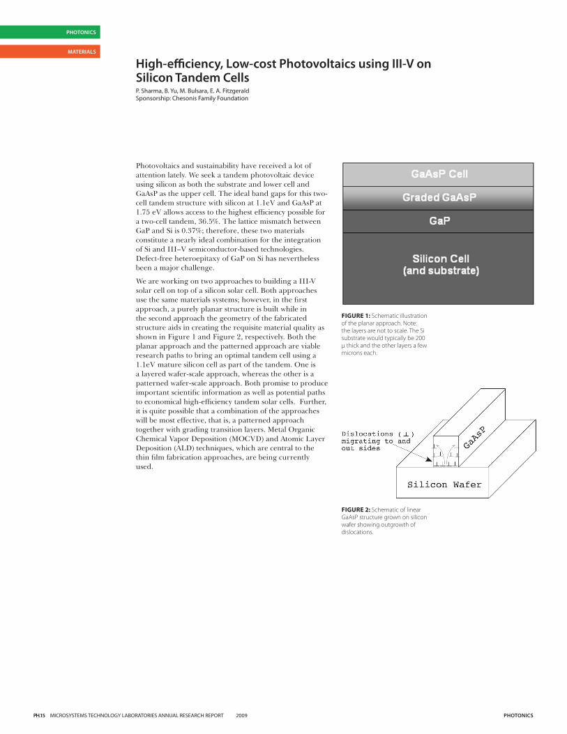
Photovoltaics and sustainability have received a lot of attention lately. We seek a tandem photovoltaic device using silicon as both the substrate and lower cell and GaAsP as the upper cell. The ideal band gaps for this two-cell tandem structure with silicon at 1.1eV and GaAsP at 1.75 eV allows access to the highest efficiency possible for a two-cell tandem, 36.5%. The lattice mismatch between GaP and Si is 0.37%; therefore, these two materials constitute a nearly ideal combination for the integration of Si and III–V semiconductor-based technologies. Defect-free heteroepitaxy of GaP on Si has nevertheless been a major challenge.
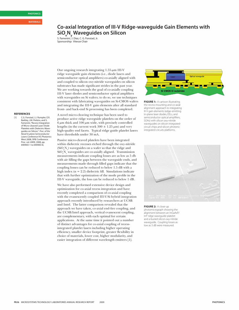
We are working on two approaches to building a III-V solar cell on top of a silicon solar cell. Both approaches use the same materials systems; however, in the first approach, a purely planar structure is built while in the second approach the geometry of the fabricated structure aids in creating the requisite material quality as shown in Figure 1 and Figure 2, respectively. Both the planar approach and the patterned approach are viable research paths to bring an optimal tandem cell using a 1.1eV mature silicon cell as part of the tandem. One is a layered wafer-scale approach, whereas the other is a patterned wafer-scale approach. Both promise to produce important scientific information as well as potential paths to economical high-efficiency tandem solar cells. Further, it is quite possible that a combination of the approaches will be most effective, that is, a patterned approach together with grading transition layers. Metal Organic Chemical Vapor Deposition (MOCVD) and Atomic Layer Deposition (ALD) techniques, which are central to the thin film fabrication approaches, are being currently used.
FIGURE 1: Schematic illustration of the planar approach. Note: the layers are not to scale. The Si substrate would typically be 200 µ thick and the other layers a few microns each.
FIGURE 2: Schematic of linear GaAsP structure grown on silicon wafer showing outgrowth of dislocations.
PH.16 MICROSYSTEMS TECHNOLOGY LABORATORIES ANNUAL RESEARCH REPORT 2009 PHotonics
PHotonics
MAtERiALs
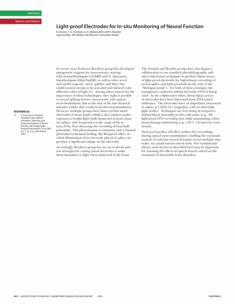
co-axial integration of iii-V Ridge-waveguide Gain Elements with sioxny Waveguides on siliconS. Famenini, J. Diaz, C. G. Fonstad, Jr.Sponsorship: Vitesse Chair
Our ongoing research integrating 1.55-µm III-V ridge waveguide gain elements (i.e., diode lasers and semiconductor optical amplifiers) co-axially aligned with and coupled to silicon oxy-nitride waveguides on silicon substrates has made significant strides in the past year. We are working towards the goal of co-axially coupling III-V laser diodes and semiconductor optical amplifiers with waveguides on Si wafers; to do so, we use techniques consistent with fabricating waveguides on Si-CMOS wafers and integrating the III-V gain elements after all standard front- and back-end Si processing has been completed.
A novel micro-cleaving technique has been used to produce active ridge waveguide platelets on the order of 6 µm thick and 100 µm wide, with precisely controlled lengths (in the current work 300 ± 1.25 µm) and very high-quality end facets. Typical ridge guide platelet lasers have thresholds under 30 mA.
Passive micro-cleaved platelets have been integrated within dielectric recesses etched through the oxy-nitride (SiOxNy) waveguides on a wafer so that the ridge and SiOxNy waveguides are co-axially aligned. Transmission measurements indicate coupling losses are as low as 5 db with air filling the gaps between the waveguide ends, and measurements made through filled gaps indicate that the coupling losses can be reduced to below 1.5 dB with a high index (n = 2.2) dielectric fill. Simulations indicate that with further optimization of the mode profile in the III-V waveguide, the loss can be reduced to below 1 dB.
We have also performed extensive device design and optimization for co-axial recess integration and have recently completed a comparison of co-axial coupling with the evanescently coupled III-V/Si hybrid integration approach recently introduced by researchers at UCSB and Intel. The latter comparison revealed that the approach we have taken, co-axial end-fire coupling, and the UCSB/Intel approach, vertical evanescent coupling, are complementary, with each optimal for certain applications. At the same time it pointed out a number of distinct advantages for co-axial coupling of recess-integrated platelet lasers including higher operating efficiency, smaller device footprint, greater flexibility in choice of materials, lower cost, higher modularity, and easier integration of different wavelength emitters [1].
FIGURE 1: A cartoon illustrating the recess-mounting and co-axial alignment approach to integrating III-V gain elements (edge-emitting in-plane laser diodes, EELs, and semiconductor optical amplifiers, SOAs) with silicon oxy-nitride waveguides on silicon integrated-circuit chips and silicon photonic integrated-circuits platforms.
FIGURE 2: A close-up photomicrograph showing the alignment between an InGaAsP/InP ridge waveguide platelet and a buried silicon oxy-nitride waveguide. Coupling losses as low as 3 dB were measured.
REFERENCES[1] C.G. Fonstad, J.J. Rumpler, E.R.
Barkley, J.M. Perkins, and S. Famenini, “Recess Integration of Micro-cleaved Laser Diode Platelets with Dielectric Wave-guides on Silicon,” Proc. of the Novel In-plane Semiconductor Lasers Conference VII, Photonics West 2008, SPIE Conference Proc. vol. 6909, 2008, pp. 69090O-1 to 69090O-8,
PH.17 MICROSYSTEMS TECHNOLOGY LABORATORIES ANNUAL RESEARCH REPORT 2009 PHotonics
PHotonics
MEDicAL ELEctRonics
Light-proof Electrodes for in-situ Monitoring of neural Function A. Zorzos, C. G. Fonstad, Jr. in collaboration with E. BoydenSponsorship: MIT Media Lab Director’s Innovator Award
In recent years Professor Boyden’s group has developed optogenetic reagents for neuroscience, starting with channelrhodopsin-2 (ChR2) and N. pharaonis halorhodopsin (Halo/NpHR), as well as other novel and useful reagents (Arch, spHalo, and Mac) that enable neural circuits to be activated and silenced with different colors of light [1]. Among other reasons for the importance of these technologies, they make it possible to record spiking activity concurrently with optical neuromodulation, due to the lack of the fast electrical stimulus artifact that results from electrical stimulation. However, multiple groups have observed that metal electrodes of many kinds exhibit a slow artifacts under exposure to bright light while immersed in brain tissue (or saline), with frequencies in the range of Hz to tens of Hz, thus obscuring the recording of local field potentials. This phenomenon is consistent with a classical photoelectrochemical finding, the Becquerel effect, in which illumination of an electrode placed in saline can produce a significant voltage on the electrode.
Accordingly, Boyden’s group has set out to devise and test strategies for coating metal electrodes to make them insensitive to light when immersed in the brain.
The Fonstad and Boyden groups have also begun a collaboration to use standard photolithographic and micro-fabrication techniques to produce linear arrays of light-proof electrodes for high-density recording of neural spikes and field potentials (in the style of the “Michigan probe”). For both of these strategies, the transparent conductor indium tin oxide (ITO) is being used. In the collaborative effort, dense linear arrays of electrodes have been fabricated from ITO-coated substrates. The electrodes have an impedance (measured in saline, at 1 kHz) of 1 megaohm, with no detectable light artifact. Techniques are now being developed to fashion linear insertable probes with many (e.g., 40) light-proof ITO recording sites while maintaining a thin, tissue-damage-minimizing (e.g., 150 × 150 micron) cross-section.
Such novel probes will allow artifact-free recordings during optical neuro-modulation, enabling the systematic analysis of real-time neural dynamics across multiple time scales, via causal neural control tools. For translational efforts, such devices as described here may be important for assessing the effects of optical neural control on the treatment of intractable brain disorders.
REFERENCES[1] X. Han and E.S. Boyden,
“Multiple-Color Optical Activation, Silencing, and Desynchronization of Neural Activity, with Single-Spike Temporal Resolution,” PLoS ONE vol. 2, no. 3, p. e299, March 2007.
PH.18 MICROSYSTEMS TECHNOLOGY LABORATORIES ANNUAL RESEARCH REPORT 2009 PHotonics
PHotonics
ELEctRonic DEVicEs
Low-threshold Vertical cavity surface-emitting Lasers Recess- integrated within silicon cMos integrated circuitsJ. M. Perkins, C. G. Fonstad, Jr.Sponsorship: NSF
Optoelectronic devices intimately integrated on silicon integrated circuits have long been sought for optical intercon-nect applications in an effort to improve data transfer rates in high performance circuits. A new heterogeneous integration technique for integrating vertical-cavity surface-emitting lasers (VCSELs) on silicon CMOS integrated circuits for such applications has been developed and demonstrated for the first time in our group at MIT [1], [2].
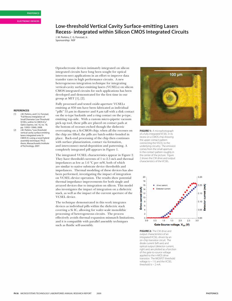
Fully processed and tested oxide-aperture VCSELs emitting at 850 nm have been fabricated as individual “pills” 55 µm in diameter and 8 µm tall with a disk contact on the n-type backside and a ring contact on the p-type, emitting top-side. With a custom micro-pipette vacuum pick-up tool, these pills are placed on contact pads at the bottom of recesses etched though the dielectric overcoating on a Si-CMOS chip; when all the recesses on the chip are filled, the pills are batch-solder-bonded in place. Back-end processing of the chip then continues with surface planarization, contact via formation, and interconnect metal-deposition and patterning. A completely integrated pill appears in Figure 1.
The integrated VCSEL characteristics appear in Figure 2. They have threshold currents of 1 to 2.5 mA and thermal impedances as low as 1.6 °C per mW, both of which are similar to native substrate device thresholds and impedances. Thermal modeling of these devices has also been performed, investigating the impact of integration on VCSEL-device operation. The results show potential thermal impedance improvements for both single and arrayed devices due to integration on silicon. This model also investigates the impact of integration on a dielectric stack, as well as the impact of the current aperture of the VCSEL device.
The technique demonstrated in this work integrates devices as individual pills within the dielectric stack covering a Si IC, allowing for wafer-scale monolithic processing of heterogeneous circuits. The process effectively avoids thermal expansion mismatch limitations, and it is compatible with parallel assembly techniques such as fluidic self-assembly.
FIGURE 1: A microphotograph of a fully integrated VCSEL in its recess on a CMOS chip showing the upper contact pattern connecting the VSCEL to the underlying circuitry. The emission comes from the small aperture in the contact pattern roughly in the center of the picture. Figure 2 shows the CW drive and output characteristics of the VCSEL.
FIGURE 2: The CW drive and output characteristics of an integrated VCSEL driven by an on-chip transistor circuit. The diode current (left axis) and optical output (detector current, right axis) are plotted as a function of the gate-to-source voltage applied to the n-MOS drive transistor. The MOSFET threshold voltage is ~ 1 V, and the VCSEL threshold is ~ 2 mA.
REFERENCES[1] J.M. Perkins, and C.G. Fonstad,
“Full Recess Integration of Small Diameter Low Threshold VCSELs within Si-CMOS ICs,” Optics Express, vol. 16, no. 18, pp. 13955-13960, 2008.
[2] J.M. Perkins, “Low threshold vertical cavity surface emitting lasers integrated onto Si-CMOS ICs using a novel hybrid assembly technique,” Ph.D. thesis, Massachusetts Institute of Technology, 2007.
PH.19 MICROSYSTEMS TECHNOLOGY LABORATORIES ANNUAL RESEARCH REPORT 2009 PHotonics
PHotonics
ELEctRonic DEVicEs
Micro-cleaved Laser Diode Platelets integrated on siliconJ. Rumpler, C. G. Fonstad, Jr.Sponsorship: DARPA through ARL; Lincoln Laboratory IPI Program
Thin (6-µm) InP-based multiple-quantum-well (MQW) ridge laser platelets emitting at a wavelength of 1550 nm have been manufactured and integrated by metal-to-metal bonding onto silicon substrates. These laser platelets can be thought of as freestanding optoelectronic building blocks that can be integrated as desired on diverse substrates. These blocks are fully processed lasers, with both top-side and bottom-side electrical contacts. The thinness of these optoelectronic building blocks and the precision with which their dimensions are defined are conducive to assembling them in dielectric recesses on a substrate such as silicon as part of an end-fire coupled optoelectronic integration strategy [1]. They are assembled by a micro-scale pick-and-place technique that allows the blocks to be picked up individually and placed as desired on the substrate of choice. Final integration is accomplished using pressurized polymer film to hold the platelets in place as they are metal-to-metal solder-bonded to the Si substrate.
To enable the manufacture of these laser platelets, a novel micro-cleaving process technology has been developed that uses notched bars of lasers as shown in Figure 1 to accurately locate the point of cleavage. This novel micro-
cleaving process is used to simultaneously obtain both smooth end facets and precisely defined cavity lengths. As a proof of concept, this process has been shown to achieve nominal cavity lengths of 300 µm +/- 1.25 µm. We believe that this micro-cleaving process can be used to make thin platelet lasers having much shorter cavity lengths and that with minor adjustments it can be used to achieve better-than-1-µm-length precision.
For the 300-µm-long, 6-µm-thin, micro-cleaved ridge platelet lasers integrated onto silicon substrates, as shown in Figure 2, continuous-wave lasing at temperatures as high as 55˚C and pulsed lasing at temperatures to at least 80˚C have been achieved. These lasers have output powers as high as 26.8 mW (at T = 10.3˚C), differential efficiencies as high as 81% (at T = 10.3˚C), and threshold currents as low as 18 mA (at T = 10.3˚C). The characteristic temperatures, T0 and T1, of the lasers on silicon were 43 K and 85 K, respectively. The thin micro-cleaved ridge platelet lasers integrated onto silicon outperformed conventionally cleaved multiple-quantum-well (MQW) ridge lasers on their native InP substrate in terms of thermal characteristics, output power, and differential efficiency [2].
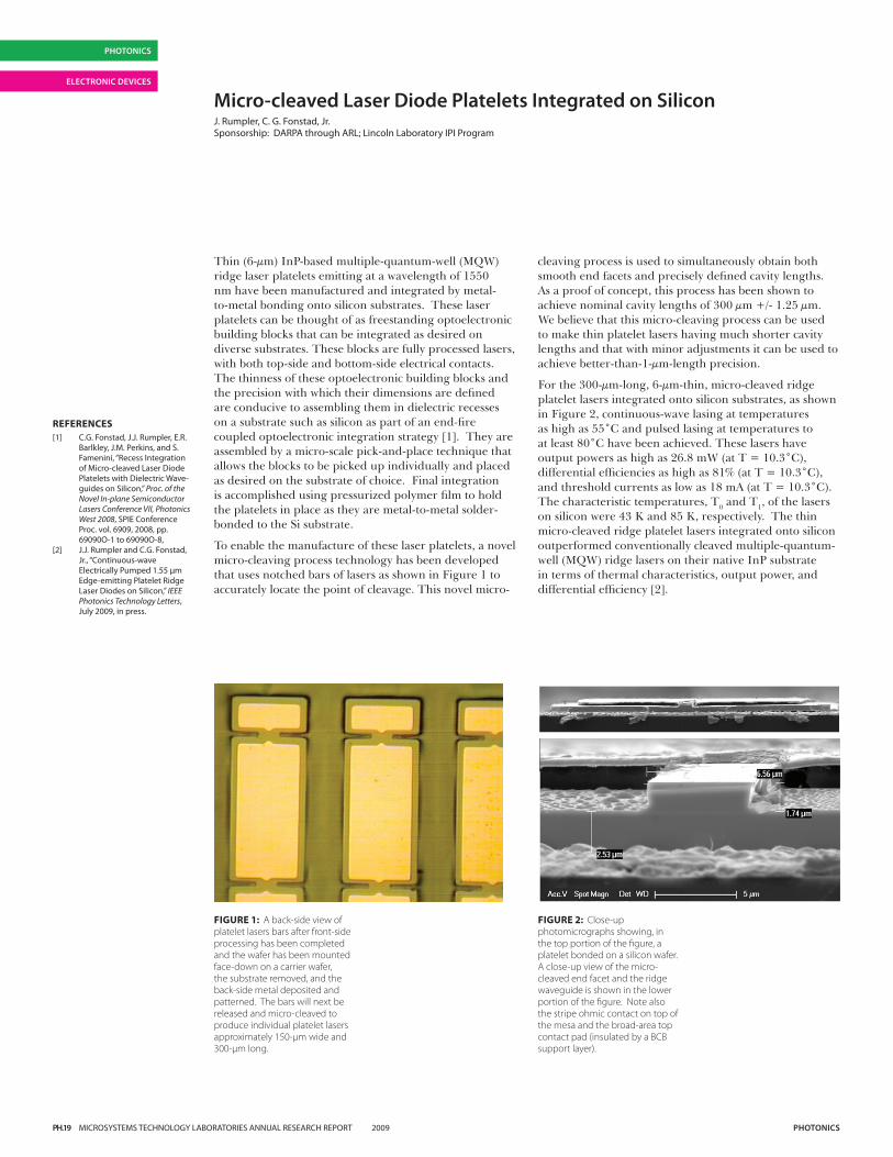
FIGURE 1: A back-side view of platelet lasers bars after front-side processing has been completed and the wafer has been mounted face-down on a carrier wafer, the substrate removed, and the back-side metal deposited and patterned. The bars will next be released and micro-cleaved to produce individual platelet lasers approximately 150-µm wide and 300-µm long.
FIGURE 2: Close-up photomicrographs showing, in the top portion of the figure, a platelet bonded on a silicon wafer. A close-up view of the micro-cleaved end facet and the ridge waveguide is shown in the lower portion of the figure. Note also the stripe ohmic contact on top of the mesa and the broad-area top contact pad (insulated by a BCB support layer).
REFERENCES[1] C.G. Fonstad, J.J. Rumpler, E.R.
Barlkley, J.M. Perkins, and S. Famenini, “Recess Integration of Micro-cleaved Laser Diode Platelets with Dielectric Wave-guides on Silicon,” Proc. of the Novel In-plane Semiconductor Lasers Conference VII, Photonics West 2008, SPIE Conference Proc. vol. 6909, 2008, pp. 69090O-1 to 69090O-8,
[2] J.J. Rumpler and C.G. Fonstad, Jr., “Continuous-wave Electrically Pumped 1.55 µm Edge-emitting Platelet Ridge Laser Diodes on Silicon,” IEEE Photonics Technology Letters, July 2009, in press.
PH.20 MICROSYSTEMS TECHNOLOGY LABORATORIES ANNUAL RESEARCH REPORT 2009 PHotonics
PHotonics
MEDicAL ELEctRonics
Waveguide Micro-probes for optical control of Excitable cells A. Zorzos, C. G. Fonstad, Jr. in collaboration with E. BoydenSponsorship: MIT Media Lab Director’s Innovator Award
Professor Ed Boyden uses light to precisely control aberrant neuron activity. His lab has invented safe, effective ways to deliver light-gated membrane proteins to neurons and other excitable cells (e.g., muscle, immune cells, pancreatic cells, etc.) in an enduring fashion, thus making the cells permanently sensitive to being activated or silenced by millisecond-timescale pulses of blue and yellow light, respectively [1]. This ability to modulate neural activity with a temporal precision that approaches that of the neural code itself holds great promise for human health, and his lab has developed animal models of epilepsy and Parkinson’s disease to explore the use of optical control to develop new therapies. His work has attracted international attention and appeared in numerous articles, including a recent piece in the Science Times section of The New York Times [2] and a profile of his lab for the Discovery Channel’s “Top 5 Science Stories of the Year.”
Professors Boyden and Fonstad have initiated a collaborative effort to use heterogeneous integration techniques developed in Fonstad’s laboratory to construct miniature linear probes to deliver light to activate and silence neural target regions along their length as desired. The goal is to develop mass-fabricatable multiple light guide microstruc-tures produced using standard microfabrication techniques. Each probe is a 200- to 250-micron-wide insertable micro-structure comprising many miniature lightguides running in parallel and delivering light to many points along the axis
of insertion. Such a design maximizes the flexibility and power of optical neural control while minimizing tissue damage. By building 2-D arrays of such probes, we can deliver multiple colors of light to 3-dimensional patterns in the brain, at the resolution of tens to hundreds of microns, thus furthering the causal analysis of complex neural circuits and dynamics. Such devices will allow the substrates that causally contribute to neurological and psychiatric disorders to be systematically analyzed via causal neural control tools. Given recent efforts on testing such reagents in nonhuman primates, these devices may also enable a new generation of optical neural control prosthetics, contributing directly to the alleviation of intractable brain disorders.
The initial light-guide structures have been fabricated from silicon nitride clad with silicon dioxide, and tests show good transmission of red light with no visible loss in the taper and bend regions of the patterns. Significantly, the novel 90˚ bend invented to direct light laterally out the side of the narrow probe (visible in both Figures 1 and 2) appears to function as designed, although much more work is needed to fully quantify the performance. The test mask contains a variety of guide structures and a series of measurements is underway to quantify the losses in straight sections of various widths, through different radius bends and sections with different degrees of taper and around the 90˚ bends. Work on the fabrication of visible-emitting platelet laser diodes to be integrated with the guides will also begin soon.
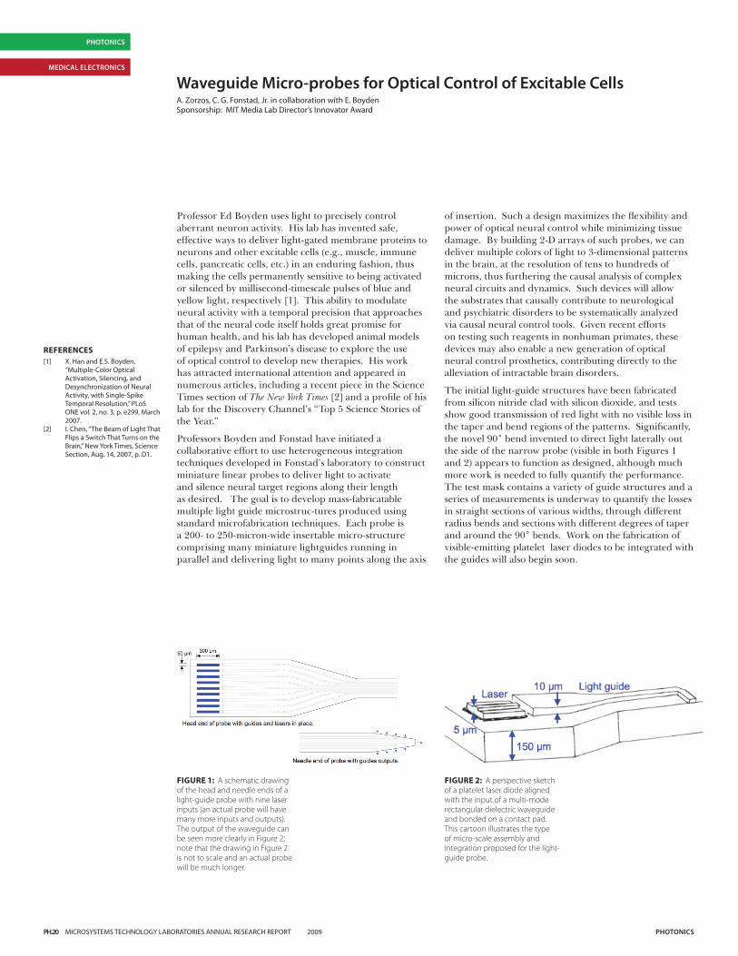
FIGURE 1: A schematic drawing of the head and needle ends of a light-guide probe with nine laser inputs (an actual probe will have many more inputs and outputs). The output of the waveguide can be seen more clearly in Figure 2; note that the drawing in Figure 2 is not to scale and an actual probe will be much longer.
FIGURE 2: A perspective sketch of a platelet laser diode aligned with the input of a multi-mode rectangular dielectric waveguide and bonded on a contact pad. This cartoon illustrates the type of micro-scale assembly and integration proposed for the light-guide probe.
REFERENCES[1] X. Han and E.S. Boyden,
“Multiple-Color Optical Activation, Silencing, and Desynchronization of Neural Activity, with Single-Spike Temporal Resolution,” PLoS ONE vol. 2, no. 3, p. e299, March 2007.
[2] I. Chen, “The Beam of Light That Flips a Switch That Turns on the Brain,” New York Times, Science Section, Aug. 14, 2007, p. D1.
PH.21 MICROSYSTEMS TECHNOLOGY LABORATORIES ANNUAL RESEARCH REPORT 2009 PHotonics
PHotonics
Development of terahertz Quantum-cascade LasersS. Kumar, A. Lee, A. Hsu, Q. Qin, T. Kao, D. Burghoff, I. Chan, Q. Hu, in collaboration with J. Reno, Sandia National Lab.Sponsorship: NSF, NASA, AFOSR, DOD NGSEG fellowship
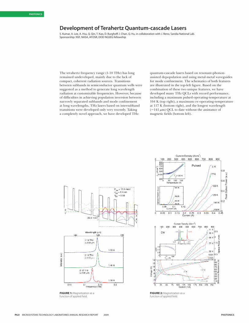
The terahertz frequency range (1-10 THz) has long remained undeveloped, mainly due to the lack of compact, coherent radiation sources. Transitions between subbands in semiconductor quantum wells were suggested as a method to generate long wavelength radiation at customizable frequencies. However, because of difficulties in achieving population inversion between narrowly separated subbands and mode confinement at long wavelengths, THz lasers based on intersubband transitions were developed only very recently. Taking a completely novel approach, we have developed THz
quantum-cascade lasers based on resonant-phonon-assisted depopulation and using metal-metal waveguides for mode confinement. The schematics of both features are illustrated in the top-left figure. Based on the combination of these two unique features, we have developed many THz QCLs with record performance, including a maximum pulsed-operating-temperature at 164 K (top right), a maximum cw-operating-temperature at 117 K (bottom right), and the longest wavelength (~141 µm) QCL to date without the assistance of magnetic fields (bottom left).
FIGURE 2: Magnetization as a function of applied field.
FIGURE 1: Magnetization as a function of applied field.
PH.22 MICROSYSTEMS TECHNOLOGY LABORATORIES ANNUAL RESEARCH REPORT 2009 PHotonics
PHotonics
MAtERiALs
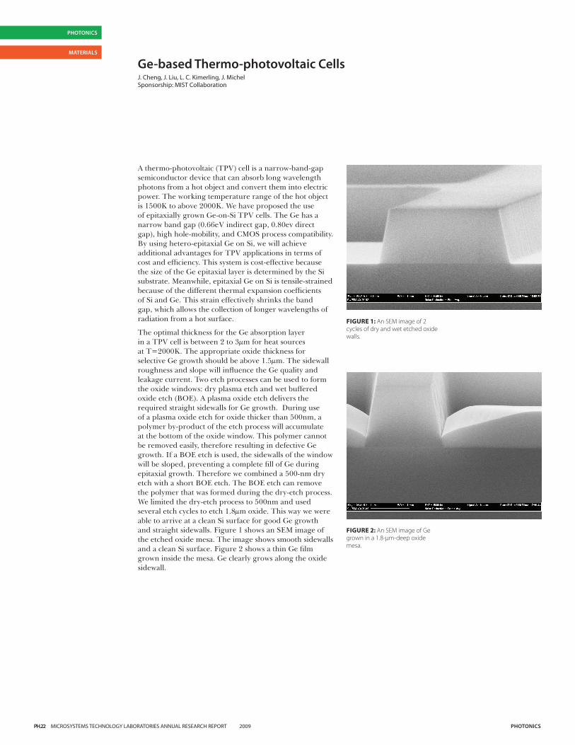
Ge-based thermo-photovoltaic cellsJ. Cheng, J. Liu, L. C. Kimerling, J. MichelSponsorship: MIST Collaboration
A thermo-photovoltaic (TPV) cell is a narrow-band-gap semiconductor device that can absorb long wavelength photons from a hot object and convert them into electric power. The working temperature range of the hot object is 1500K to above 2000K. We have proposed the use of epitaxially grown Ge-on-Si TPV cells. The Ge has a narrow band gap (0.66eV indirect gap, 0.80ev direct gap), high hole-mobility, and CMOS process compatibility. By using hetero-epitaxial Ge on Si, we will achieve additional advantages for TPV applications in terms of cost and efficiency. This system is cost-effective because the size of the Ge epitaxial layer is determined by the Si substrate. Meanwhile, epitaxial Ge on Si is tensile-strained because of the different thermal expansion coefficients of Si and Ge. This strain effectively shrinks the band gap, which allows the collection of longer wavelengths of radiation from a hot surface.
The optimal thickness for the Ge absorption layer in a TPV cell is between 2 to 3µm for heat sources at T=2000K. The appropriate oxide thickness for selective Ge growth should be above 1.5µm. The sidewall roughness and slope will influence the Ge quality and leakage current. Two etch processes can be used to form the oxide windows: dry plasma etch and wet buffered oxide etch (BOE). A plasma oxide etch delivers the required straight sidewalls for Ge growth. During use of a plasma oxide etch for oxide thicker than 500nm, a polymer by-product of the etch process will accumulate at the bottom of the oxide window. This polymer cannot be removed easily, therefore resulting in defective Ge growth. If a BOE etch is used, the sidewalls of the window will be sloped, preventing a complete fill of Ge during epitaxial growth. Therefore we combined a 500-nm dry etch with a short BOE etch. The BOE etch can remove the polymer that was formed during the dry-etch process. We limited the dry-etch process to 500nm and used several etch cycles to etch 1.8µm oxide. This way we were able to arrive at a clean Si surface for good Ge growth and straight sidewalls. Figure 1 shows an SEM image of the etched oxide mesa. The image shows smooth sidewalls and a clean Si surface. Figure 2 shows a thin Ge film grown inside the mesa. Ge clearly grows along the oxide sidewall.
FIGURE 1: An SEM image of 2 cycles of dry and wet etched oxide walls.
FIGURE 2: An SEM image of Ge grown in a 1.8-μm-deep oxide mesa.
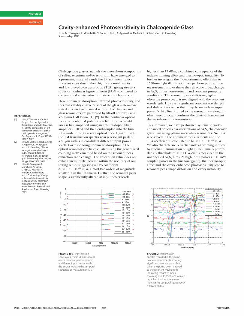
PH.23 MICROSYSTEMS TECHNOLOGY LABORATORIES ANNUAL RESEARCH REPORT 2009 PHotonics
PHotonics
MAtERiALs
cavity-enhanced Photosensitivity in chalcogenide GlassJ. Hu, M. Torregiani, F. Morichetti, N. Carlie, L. Petit, A. Agarwal, A. Melloni, K. Richardson, L. C. KimerlingSponsorship: DOE
Chalcogenide glasses, namely the amorphous compounds of sulfur, selenium and/or tellurium, have emerged as a promising material candidate for nonlinear optics in recent years due to their high Kerr nonlinearity and low two-photon absorption (TPA), giving rise to a superior nonlinear figure of merit (FOM) compared to conventional semiconductor materials such as silicon.
Here nonlinear absorption, infrared photosensitivity, and thermal stability characteristics of the glass material are tested in a cavity-enhanced setting. The chalcogenide glass resonators are patterned by lift-off entirely using a 500-nm CMOS line [1], [2]. In the nonlinear optical measurements, TM polarization light from a tunable laser is first amplified using an erbium-doped fiber amplifier (EDFA) and then end-coupled into the bus-waveguide through a silica optical fiber. Figure 1 plots the TM transmission spectra near a resonant peak of a 30-µm radius micro-disk at different input power levels. Corresponding nonlinear absorption in the optical resonator can be calculated using the generalized coupling matrix method based on the resonant peak extinction ratio change. The absorption value does not exhibit measurable increase within the accuracy of our testing setup, suggesting a TPA coefficient α2 < 1.5 × 10⁻¹³ m/W, almost two orders of magnitude smaller than that of silicon. Further, the resonant peak shape is significantly altered at input power levels
higher than 17 dBm, a combined consequence of the index-trimming effect and thermo-optic instability. To further investigate the index-trimming effect due to 1550-nm light illumination, we perform pump-probe measurements to evaluate the refractive index change in As2S3 under non-resonant and resonant pumping conditions,. The resonant peak shift is negligible when the pump beam is not aligned with the resonant wavelength. However, significant resonant wavelength red shift is observed as the pump beam with an input power > 14 dBm is tuned to the resonant wavelength, which unequivocally confirms the cavity-enhancement due to infrared photosensitivity.
To summarize, we have performed systematic cavity-enhanced optical characterizations of As2S3 chalcogenide glass films using planar micro-disk resonators. No TPA is observed in the nonlinear measurements and the TPA coefficient is calculated to be < 1.5 × 10⁻¹³ m/W. We also characterize refractive index-trimming induced by resonant illumination of light at 1550 nm. A power- density threshold of < 0.1 GW/cm2 is measured in the unannealed As2S3 films. At high input power (~ 10 mW coupled power in the bus waveguide), the thermo-optic effect and the cavity-enhanced photosensitivity lead to resonant peak shape distortion and cavity instability.
1552.9 1552.95 1553 1553.05 1553.1-45
-40
-35
-30
-25
-20
-15
-10
-5
0
5
Wavelength (nm)
Transmission (dB) -10.9 dBm
-5.9 dBm-0.9 dBm4.1 dBm9.1 dBm11.6 dBm14.1 dBm15.1 dBm16.1 dBm17.1 dBm18.1 dBm19.1 dBm20.1 dBm21.1 dBm22.1 dBm23.1 dBm
FIGURE 1: (a) Transmission spectra of a micro-disk resonator near a resonant peak measured at different input power levels; the arrows indicate the temporal sequence of measurements. [3]
FIGURE 2: Transmission spectra recorded in the pump-probe measurements showing significant resonant peak shift when the pump beam is tuned to the resonant wavelength, indicating refractive index trimming due to 1550-nm infrared light illumination; the arrows indicate the temporal sequence of measurements.
REFERENCES[1] J. Hu, V. Tarasov, N. Carlie, N.
Feng, L. Petit, A. Agarwal, K. Richardson, and L. C. Kimerling, “Si-CMOS-compatible lift-off fabrication of low-loss planar chalcogenide waveguides,” Opt. Express vol. 15, pp. 11798-11807, 2007.
[2] J. Hu, N. Carlie, N. Feng, L. Petit, A. Agarwal, K. Richardson, and L. C. Kimerling, “Planar waveguide-coupled, high-index-contrast, high-Q resonators in chalcogenide glass for sensing,” Opt. Lett. vol. 33, pp. 2500-2502, 2008.
[3] J. Hu, M. Torregiani, F. Morichetti, N. Carlie, L. Petit, A. Agarwal, A. Melloni, K. Richardson, and L.C. Kimerling, “Cavity-enhanced photosensitivity in chalcogenide glass,” OSA Integrated Photonics and Nanophotonics Research and Applications Topical Meeting, 2009.
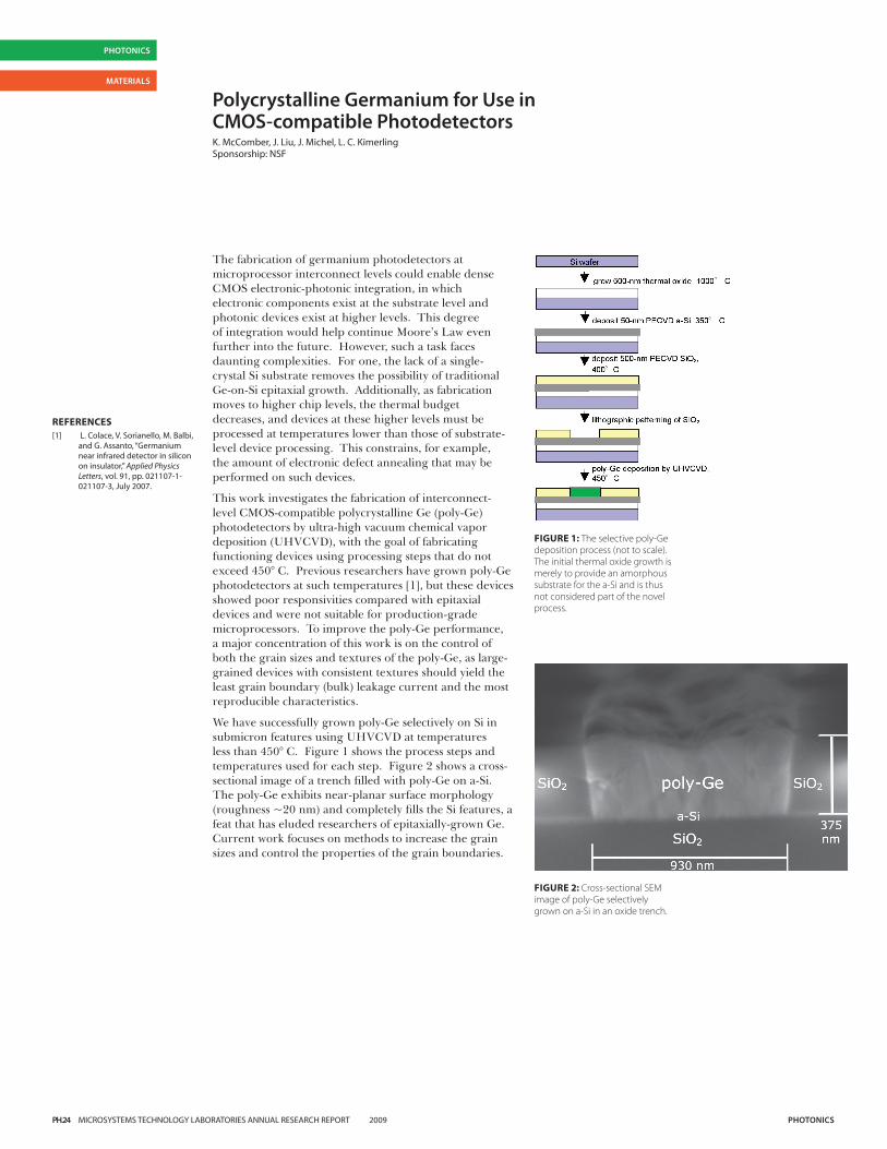
PH.24 MICROSYSTEMS TECHNOLOGY LABORATORIES ANNUAL RESEARCH REPORT 2009 PHotonics
PHotonics
MAtERiALs
Polycrystalline Germanium for Use in cMos-compatible Photodetectors K. McComber, J. Liu, J. Michel, L. C. KimerlingSponsorship: NSF
The fabrication of germanium photodetectors at microprocessor interconnect levels could enable dense CMOS electronic-photonic integration, in which electronic components exist at the substrate level and photonic devices exist at higher levels. This degree of integration would help continue Moore’s Law even further into the future. However, such a task faces daunting complexities. For one, the lack of a single-crystal Si substrate removes the possibility of traditional Ge-on-Si epitaxial growth. Additionally, as fabrication moves to higher chip levels, the thermal budget decreases, and devices at these higher levels must be processed at temperatures lower than those of substrate-level device processing. This constrains, for example, the amount of electronic defect annealing that may be performed on such devices.
This work investigates the fabrication of interconnect-level CMOS-compatible polycrystalline Ge (poly-Ge) photodetectors by ultra-high vacuum chemical vapor deposition (UHVCVD), with the goal of fabricating functioning devices using processing steps that do not exceed 450° C. Previous researchers have grown poly-Ge photodetectors at such temperatures [1], but these devices showed poor responsivities compared with epitaxial devices and were not suitable for production-grade microprocessors. To improve the poly-Ge performance, a major concentration of this work is on the control of both the grain sizes and textures of the poly-Ge, as large-grained devices with consistent textures should yield the least grain boundary (bulk) leakage current and the most reproducible characteristics.
We have successfully grown poly-Ge selectively on Si in submicron features using UHVCVD at temperatures less than 450° C. Figure 1 shows the process steps and temperatures used for each step. Figure 2 shows a cross-sectional image of a trench filled with poly-Ge on a-Si. The poly-Ge exhibits near-planar surface morphology (roughness ~20 nm) and completely fills the Si features, a feat that has eluded researchers of epitaxially-grown Ge. Current work focuses on methods to increase the grain sizes and control the properties of the grain boundaries.
FIGURE 1: The selective poly-Ge deposition process (not to scale). The initial thermal oxide growth is merely to provide an amorphous substrate for the a-Si and is thus not considered part of the novel process.
FIGURE 2: Cross-sectional SEM image of poly-Ge selectively grown on a-Si in an oxide trench.
REFERENCES[1] L. Colace, V. Sorianello, M. Balbi,
and G. Assanto, “Germanium near infrared detector in silicon on insulator,” Applied Physics Letters, vol. 91, pp. 021107-1-021107-3, July 2007.
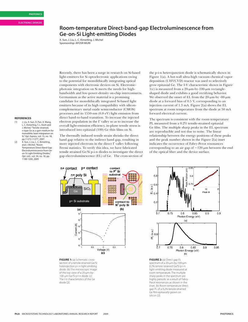
PH.25 MICROSYSTEMS TECHNOLOGY LABORATORIES ANNUAL RESEARCH REPORT 2009 PHotonics
PHotonics
ELEctRonic DEVicEs
Room-temperature Direct-band-gap Electroluminescence from Ge-on-si Light-emitting DiodesX. Sun, J. Liu, L. C. Kimerling, J. MichelSponsorship: AFOSR MURI
Recently, there has been a surge in research on Si-based light-emitters for Si optoelectronic applications owing to the potential for monolithically integrating optical components with electronic devices on Si. Electronic-photonic integration on Si meets the needs for high-bandwidth and low-power-density on-chip interconnects. Germanium as the active material is a promising candidate for monolithically integrated Si-based light emitters because of its high compatibility with silicon-complementary metal oxide semiconductor (CMOS) processes and its 1550-nm (0.8 eV) light emission from direct band-to-band transition. To increase the injected electron population in the Γ valley so as to increase the overall light-emission efficiency, in-plane tensile stress is introduced into epitaxial (100) Ge thin films on Si.
The thermally induced tensile strain shrinks the direct band gap relative to the indirect band gap, resulting in more injected electrons in the direct Γ valley following Fermi statistics. To verify this idea, we have fabricated tensile strained Ge/Si p-i-n diodes to investigate the direct gap electroluminescence (EL) of Ge. The cross-section of
the p-i-n heterojunction diode is schematically shown in Figure 1(a). A hot-wall ultra-high vacuum chemical vapor deposition (UHVCVD) reactor was used to selectively grow epitaxial Ge. The I-V characteristic shown in Figure 1(c) is measured from a 20-µm-by-100-µm rectangle-shaped diode and exhibits a good rectifying behavior. We observed the onset of EL from the 20-µm-by -00-µm diode at a forward bias of 0.5 V, corresponding to an injection current of 1.3 mA. Figure 2(a) shows the EL spectrum at room temperature from the diode at 50 mA forward electrical current.
The spectrum is consistent with the room-temperature PL measured from a 0.2% tensile-strained epitaxial Ge film. The multiple sharp peaks in the EL spectrum are reproducible and not due to noise. The linear relationship between the energy positions of these peaks and the peak number shown in the Figure 2(a) inset indicates the occurrence of Fabry-Perot resonances corresponding to an air gap of ~120 µm between the end of the optical fiber and the device surface.
FIGURE 1: (a) Schematic cross-section of a tensile-strained Ge/Si heterojection p-i-n light emitting diode. (b) The microscopic image of the top view of a 20-µm-by-100-µm Ge/Si p-i-n diode. (c) The I-V characteristics of the Ge diode [2].
FIGURE 2: (a) Direct gap EL spectrum of a 20-µm-by-100-µm 0.2% tensile-strained Ge/Si p-i-n light-emitting diode measured at room temperature. The multiple sharp peaks in the spectrum are highly periodic as a result of Fabry-Perot resonances as shown in the inset. (b) Room temperature direct gap PL of a 0.2% tensile-strained Ge film epitaxially grown on silicon [2].
REFERENCES[1] J. Liu, X. Sun, D. Pan, X. Wang,
L. C. Kimerling, T. L. Koch and J. Michel, “Tensile-strained, n-type Ge as a gain medium for monolithic laser integration on Si,” Opt. Express, vol. 15, no. 18, pp.11272-11277, 2007.
[2] X. Sun, J. Liu, L. C. Kimerling, and J. Michel, “Room Temperature Direct Band Gap Electroluminescence from Ge-on-Si Light Emitting Diodes,” Opt. Lett., vol. 34, no. 18, pp. 1198-1200, 2009
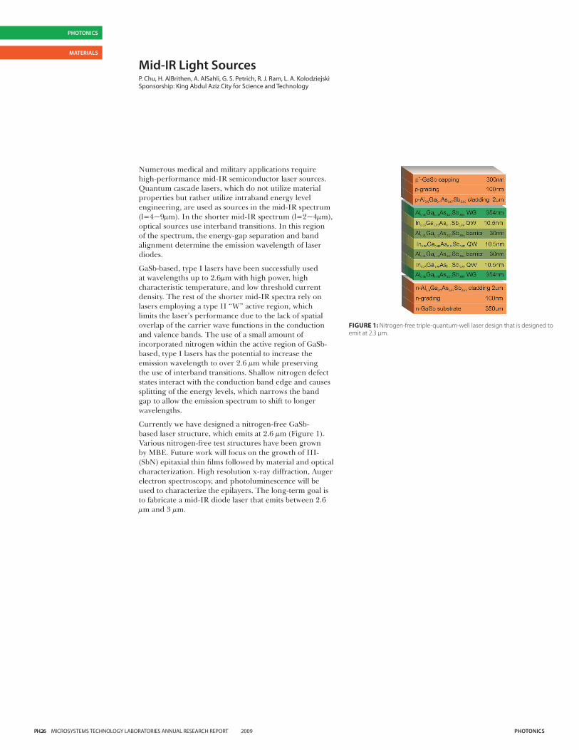
PH.26 MICROSYSTEMS TECHNOLOGY LABORATORIES ANNUAL RESEARCH REPORT 2009 PHotonics
PHotonics
MAtERiALs
Mid-iR Light sources P. Chu, H. AlBrithen, A. AlSahli, G. S. Petrich, R. J. Ram, L. A. KolodziejskiSponsorship: King Abdul Aziz City for Science and Technology
Numerous medical and military applications require high-performance mid-IR semiconductor laser sources. Quantum cascade lasers, which do not utilize material properties but rather utilize intraband energy level engineering, are used as sources in the mid-IR spectrum (l=4~9µm). In the shorter mid-IR spectrum (l=2~4µm), optical sources use interband transitions. In this region of the spectrum, the energy-gap separation and band alignment determine the emission wavelength of laser diodes.
GaSb-based, type I lasers have been successfully used at wavelengths up to 2.6µm with high power, high characteristic temperature, and low threshold current density. The rest of the shorter mid-IR spectra rely on lasers employing a type II “W” active region, which limits the laser’s performance due to the lack of spatial overlap of the carrier wave functions in the conduction and valence bands. The use of a small amount of incorporated nitrogen within the active region of GaSb-based, type I lasers has the potential to increase the emission wavelength to over 2.6 µm while preserving the use of interband transitions. Shallow nitrogen defect states interact with the conduction band edge and causes splitting of the energy levels, which narrows the band gap to allow the emission spectrum to shift to longer wavelengths.
Currently we have designed a nitrogen-free GaSb-based laser structure, which emits at 2.6 µm (Figure 1). Various nitrogen-free test structures have been grown by MBE. Future work will focus on the growth of III-(SbN) epitaxial thin films followed by material and optical characterization. High resolution x-ray diffraction, Auger electron spectroscopy, and photoluminescence will be used to characterize the epilayers. The long-term goal is to fabricate a mid-IR diode laser that emits between 2.6 µm and 3 µm.
FIGURE 1: Nitrogen-free triple-quantum-well laser design that is designed to emit at 2.3 µm.
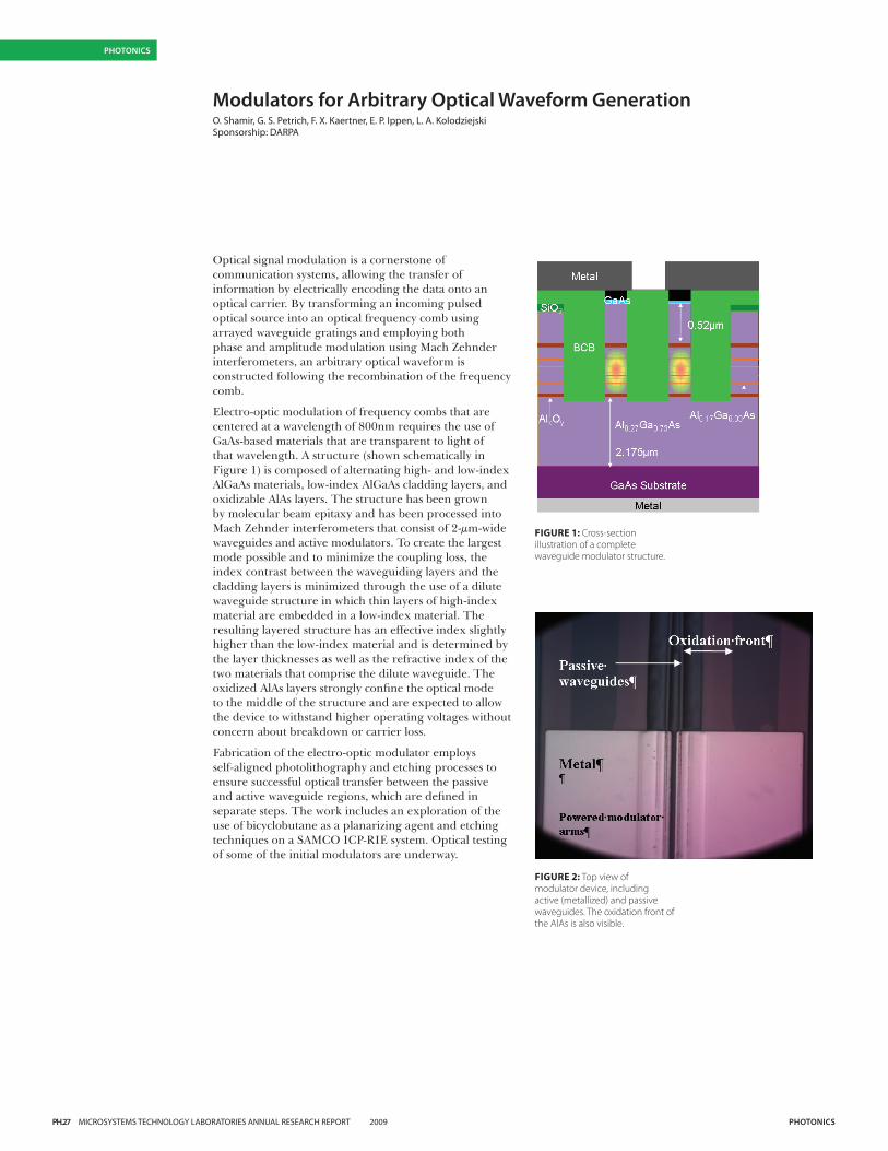
PH.27 MICROSYSTEMS TECHNOLOGY LABORATORIES ANNUAL RESEARCH REPORT 2009 PHotonics
PHotonics
Modulators for Arbitrary optical Waveform Generation O. Shamir, G. S. Petrich, F. X. Kaertner, E. P. Ippen, L. A. KolodziejskiSponsorship: DARPA
Optical signal modulation is a cornerstone of communication systems, allowing the transfer of information by electrically encoding the data onto an optical carrier. By transforming an incoming pulsed optical source into an optical frequency comb using arrayed waveguide gratings and employing both phase and amplitude modulation using Mach Zehnder interferometers, an arbitrary optical waveform is constructed following the recombination of the frequency comb.
Electro-optic modulation of frequency combs that are centered at a wavelength of 800nm requires the use of GaAs-based materials that are transparent to light of that wavelength. A structure (shown schematically in Figure 1) is composed of alternating high- and low-index AlGaAs materials, low-index AlGaAs cladding layers, and oxidizable AlAs layers. The structure has been grown by molecular beam epitaxy and has been processed into Mach Zehnder interferometers that consist of 2-µm-wide waveguides and active modulators. To create the largest mode possible and to minimize the coupling loss, the index contrast between the waveguiding layers and the cladding layers is minimized through the use of a dilute waveguide structure in which thin layers of high-index material are embedded in a low-index material. The resulting layered structure has an effective index slightly higher than the low-index material and is determined by the layer thicknesses as well as the refractive index of the two materials that comprise the dilute waveguide. The oxidized AlAs layers strongly confine the optical mode to the middle of the structure and are expected to allow the device to withstand higher operating voltages without concern about breakdown or carrier loss.
Fabrication of the electro-optic modulator employs self-aligned photolithography and etching processes to ensure successful optical transfer between the passive and active waveguide regions, which are defined in separate steps. The work includes an exploration of the use of bicyclobutane as a planarizing agent and etching techniques on a SAMCO ICP-RIE system. Optical testing of some of the initial modulators are underway.
FIGURE 1: Cross-section illustration of a complete waveguide modulator structure.
FIGURE 2: Top view of modulator device, including active (metallized) and passive waveguides. The oxidation front of the AlAs is also visible.
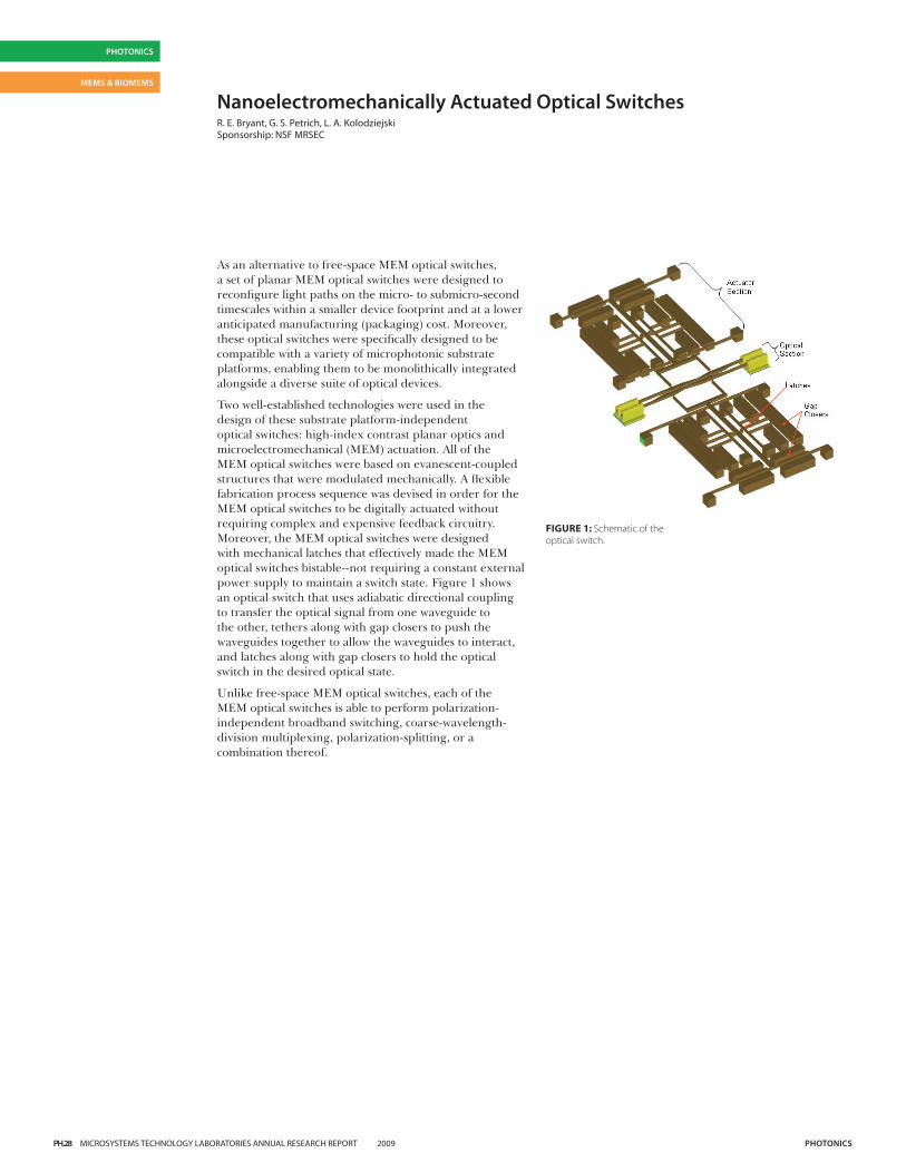
PH.28 MICROSYSTEMS TECHNOLOGY LABORATORIES ANNUAL RESEARCH REPORT 2009 PHotonics
PHotonics
MEMs & BioMEMs
nanoelectromechanically Actuated optical switchesR. E. Bryant, G. S. Petrich, L. A. KolodziejskiSponsorship: NSF MRSEC
As an alternative to free-space MEM optical switches, a set of planar MEM optical switches were designed to reconfigure light paths on the micro- to submicro-second timescales within a smaller device footprint and at a lower anticipated manufacturing (packaging) cost. Moreover, these optical switches were specifically designed to be compatible with a variety of microphotonic substrate platforms, enabling them to be monolithically integrated alongside a diverse suite of optical devices.
Two well-established technologies were used in the design of these substrate platform-independent optical switches: high-index contrast planar optics and microelectromechanical (MEM) actuation. All of the MEM optical switches were based on evanescent-coupled structures that were modulated mechanically. A flexible fabrication process sequence was devised in order for the MEM optical switches to be digitally actuated without requiring complex and expensive feedback circuitry. Moreover, the MEM optical switches were designed with mechanical latches that effectively made the MEM optical switches bistable--not requiring a constant external power supply to maintain a switch state. Figure 1 shows an optical switch that uses adiabatic directional coupling to transfer the optical signal from one waveguide to the other, tethers along with gap closers to push the waveguides together to allow the waveguides to interact, and latches along with gap closers to hold the optical switch in the desired optical state.
Unlike free-space MEM optical switches, each of the MEM optical switches is able to perform polarization-independent broadband switching, coarse-wavelength-division multiplexing, polarization-splitting, or a combination thereof.
FIGURE 1: Schematic of the optical switch.
PH.29 MICROSYSTEMS TECHNOLOGY LABORATORIES ANNUAL RESEARCH REPORT 2009 PHotonics
PHotonics
MAtERiALs
novel Active Materials for optical sourcesS. Nabanja, G. S. Petrich, L. A. KolodziejskiSponsorship: NSF
Quantum-dot (QD) heterostructure lasers are a type of semiconductor laser that utilize quantum dots as their active medium within the light-emitting region. Quantum dots are semiconductor nanocrystals of narrow band-gap material that are embedded in a wider band-gap material. The use of molecular beam epitaxy for the growth of highly lattice-mismatched III-V semiconductor materials has made the self-assembly of these structures possible. Due to the strong three-dimensional carrier confinement, devices that employ quantum dots have unique capabilities that are otherwise practically unachievable with bulk semi-conductors or even two-dimensional-confined quantum wells.
One of the significant benefits of exploiting quantum effects in QD semiconductor lasers is the decrease of the laser’s threshold current density, which is a direct result of the reduction in the translational degrees of freedom of charge-carriers (electrons and holes). This reduction in translational degrees of freedom leads to an increase in the density of states of charge-carriers near the band edges. Another important benefit is that the threshold current density in QD lasers is unaffected by
temperatures up to about 300K since the charge-carriers can only be thermally excited to a very limited number of the well-spaced energy levels.
The goal of this work is to design, fabricate, and characterize semiconductor lasers with quantum dots within their active region on both n-GaAs substrates and n-InP substrates. The use of a separate confinement heterostructure will allow for electrical and vertical optical confinement while horizontal optical confinement will be achieved by means of ridge waveguides. The front-end fabrication processes include photolithography to define the etch masks, a reactive ion and a wet etch of the arsenide-based or phosphide-based material to create the waveguide ridges, a planarization step, and then finally ohmic contact patterning. The back-end processes include lapping, metal evaporation, and cleaving. Characterization of GaAs-based quantum dot layers is underway while the etching of the phosphide layers within the InP-based quantum dot lasers is being optimized on the SAMCO inductively-coupled-plasma reactive ion etcher.
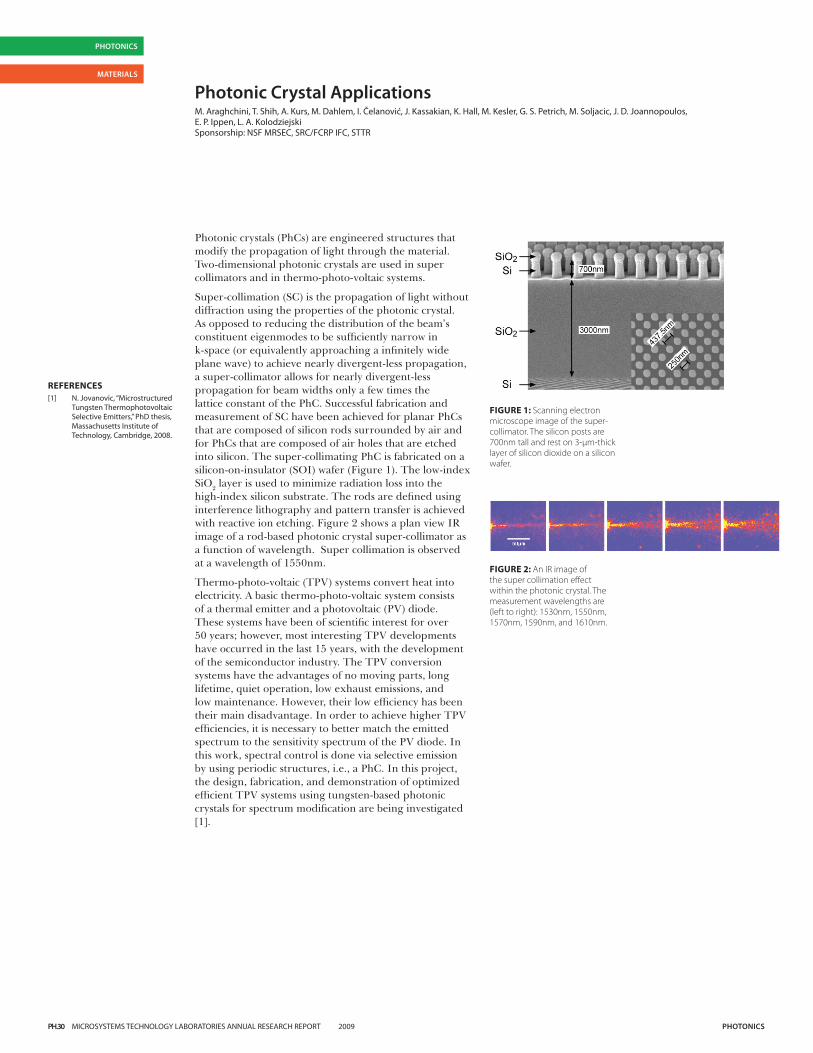
PH.30 MICROSYSTEMS TECHNOLOGY LABORATORIES ANNUAL RESEARCH REPORT 2009 PHotonics
PHotonics
MAtERiALs
Photonic crystal Applications M. Araghchini, T. Shih, A. Kurs, M. Dahlem, I. Čelanović, J. Kassakian, K. Hall, M. Kesler, G. S. Petrich, M. Soljacic, J. D. Joannopoulos, E. P. Ippen, L. A. KolodziejskiSponsorship: NSF MRSEC, SRC/FCRP IFC, STTR
Photonic crystals (PhCs) are engineered structures that modify the propagation of light through the material. Two-dimensional photonic crystals are used in super collimators and in thermo-photo-voltaic systems.
Super-collimation (SC) is the propagation of light without diffraction using the properties of the photonic crystal. As opposed to reducing the distribution of the beam’s constituent eigenmodes to be sufficiently narrow in k-space (or equivalently approaching a infinitely wide plane wave) to achieve nearly divergent-less propagation, a super-collimator allows for nearly divergent-less propagation for beam widths only a few times the lattice constant of the PhC. Successful fabrication and measurement of SC have been achieved for planar PhCs that are composed of silicon rods surrounded by air and for PhCs that are composed of air holes that are etched into silicon. The super-collimating PhC is fabricated on a silicon-on-insulator (SOI) wafer (Figure 1). The low-index SiO2 layer is used to minimize radiation loss into the high-index silicon substrate. The rods are defined using interference lithography and pattern transfer is achieved with reactive ion etching. Figure 2 shows a plan view IR image of a rod-based photonic crystal super-collimator as a function of wavelength. Super collimation is observed at a wavelength of 1550nm.
Thermo-photo-voltaic (TPV) systems convert heat into electricity. A basic thermo-photo-voltaic system consists of a thermal emitter and a photovoltaic (PV) diode. These systems have been of scientific interest for over 50 years; however, most interesting TPV developments have occurred in the last 15 years, with the development of the semiconductor industry. The TPV conversion systems have the advantages of no moving parts, long lifetime, quiet operation, low exhaust emissions, and low maintenance. However, their low efficiency has been their main disadvantage. In order to achieve higher TPV efficiencies, it is necessary to better match the emitted spectrum to the sensitivity spectrum of the PV diode. In this work, spectral control is done via selective emission by using periodic structures, i.e., a PhC. In this project, the design, fabrication, and demonstration of optimized efficient TPV systems using tungsten-based photonic crystals for spectrum modification are being investigated [1].
FIGURE 1: Scanning electron microscope image of the super-collimator. The silicon posts are 700nm tall and rest on 3-μm-thick layer of silicon dioxide on a silicon wafer.
FIGURE 2: An IR image of the super collimation effect within the photonic crystal. The measurement wavelengths are (left to right): 1530nm, 1550nm, 1570nm, 1590nm, and 1610nm.
REFERENCES[1] N. Jovanovic, “Microstructured
Tungsten Thermophotovoltaic Selective Emitters,” PhD thesis, Massachusetts Institute of Technology, Cambridge, 2008.
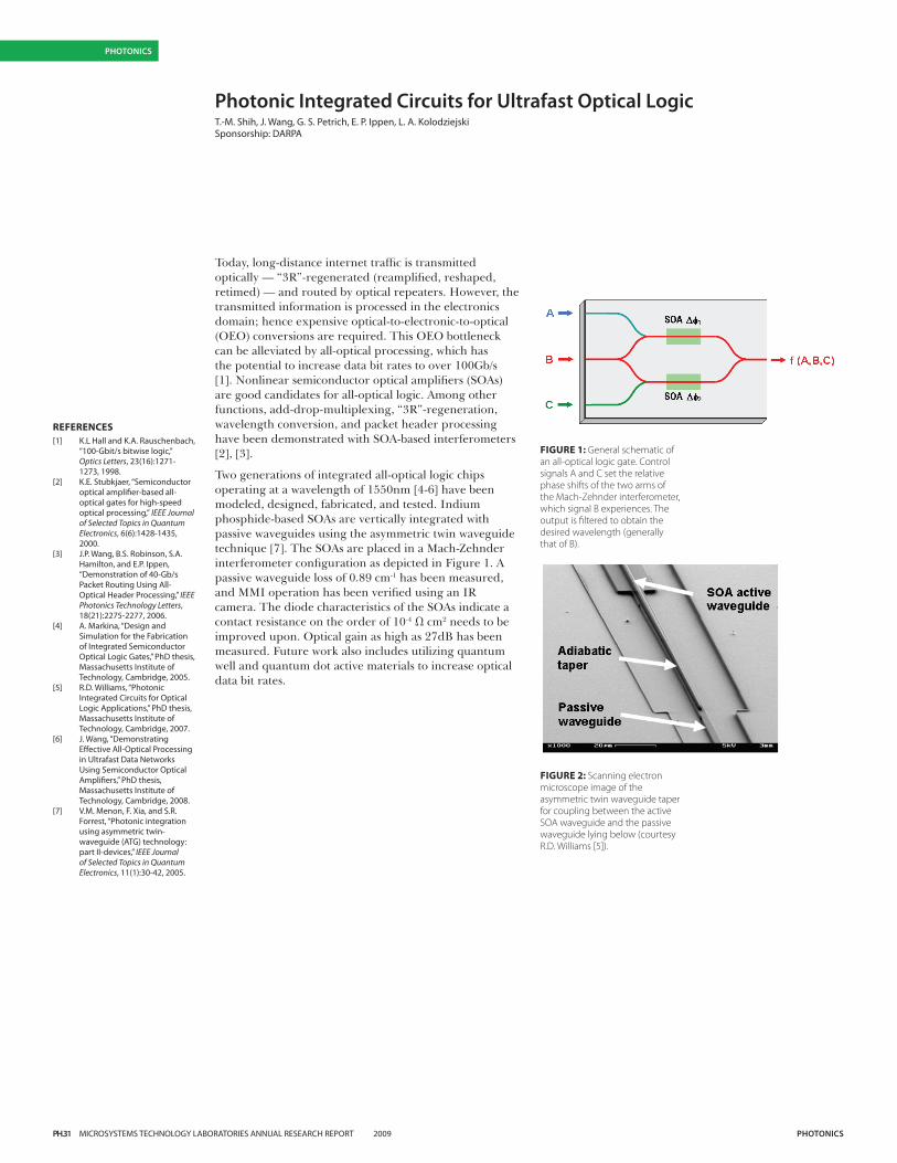
PH.31 MICROSYSTEMS TECHNOLOGY LABORATORIES ANNUAL RESEARCH REPORT 2009 PHotonics
PHotonics
Photonic integrated circuits for Ultrafast optical Logic T.-M. Shih, J. Wang, G. S. Petrich, E. P. Ippen, L. A. KolodziejskiSponsorship: DARPA
Today, long-distance internet traffic is transmitted optically — “3R”-regenerated (reamplified, reshaped, retimed) — and routed by optical repeaters. However, the transmitted information is processed in the electronics domain; hence expensive optical-to-electronic-to-optical (OEO) conversions are required. This OEO bottleneck can be alleviated by all-optical processing, which has the potential to increase data bit rates to over 100Gb/s [1]. Nonlinear semiconductor optical amplifiers (SOAs) are good candidates for all-optical logic. Among other functions, add-drop-multiplexing, “3R”-regeneration, wavelength conversion, and packet header processing have been demonstrated with SOA-based interferometers [2], [3].
Two generations of integrated all-optical logic chips operating at a wavelength of 1550nm [4-6] have been modeled, designed, fabricated, and tested. Indium phosphide-based SOAs are vertically integrated with passive waveguides using the asymmetric twin waveguide technique [7]. The SOAs are placed in a Mach-Zehnder interferometer configuration as depicted in Figure 1. A passive waveguide loss of 0.89 cm-1 has been measured, and MMI operation has been verified using an IR camera. The diode characteristics of the SOAs indicate a contact resistance on the order of 10-4 Ω cm2 needs to be improved upon. Optical gain as high as 27dB has been measured. Future work also includes utilizing quantum well and quantum dot active materials to increase optical data bit rates.
FIGURE 1: General schematic of an all-optical logic gate. Control signals A and C set the relative phase shifts of the two arms of the Mach-Zehnder interferometer, which signal B experiences. The output is filtered to obtain the desired wavelength (generally that of B).
FIGURE 2: Scanning electron microscope image of the asymmetric twin waveguide taper for coupling between the active SOA waveguide and the passive waveguide lying below (courtesy R.D. Williams [5]).
REFERENCES[1] K.L Hall and K.A. Rauschenbach,
“100-Gbit/s bitwise logic,” Optics Letters, 23(16):1271-1273, 1998.
[2] K.E. Stubkjaer, “Semiconductor optical amplifier-based all-optical gates for high-speed optical processing,” IEEE Journal of Selected Topics in Quantum Electronics, 6(6):1428-1435, 2000.
[3] J.P. Wang, B.S. Robinson, S.A. Hamilton, and E.P. Ippen, “Demonstration of 40-Gb/s Packet Routing Using All-Optical Header Processing,” IEEE Photonics Technology Letters, 18(21):2275-2277, 2006.
[4] A. Markina, “Design and Simulation for the Fabrication of Integrated Semiconductor Optical Logic Gates,” PhD thesis, Massachusetts Institute of Technology, Cambridge, 2005.
[5] R.D. Williams, “Photonic Integrated Circuits for Optical Logic Applications,” PhD thesis, Massachusetts Institute of Technology, Cambridge, 2007.
[6] J. Wang, “Demonstrating Effective All-Optical Processing in Ultrafast Data Networks Using Semiconductor Optical Amplifiers,” PhD thesis, Massachusetts Institute of Technology, Cambridge, 2008.
[7] V.M. Menon, F. Xia, and S.R. Forrest, “Photonic integration using asymmetric twin-waveguide (ATG) technology: part II-devices,” IEEE Journal of Selected Topics in Quantum Electronics, 11(1):30-42, 2005.
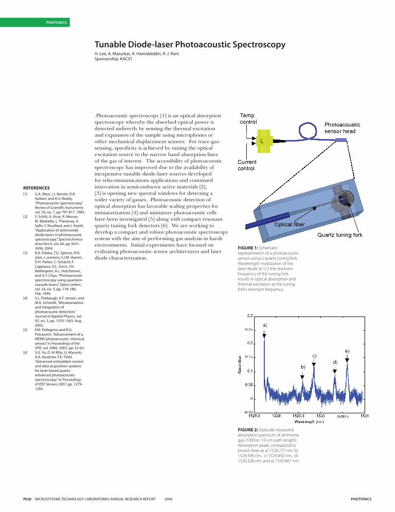
PH.32 MICROSYSTEMS TECHNOLOGY LABORATORIES ANNUAL RESEARCH REPORT 2009 PHotonics
PHotonics
tunable Diode-laser Photoacoustic spectroscopyH. Lee, A. Masurkar, A. Hamidalddin, R. J. Ram Sponsorship: KACST
.Photoacoustic spectroscopy [1] is an optical absorption spectroscopy whereby the absorbed optical power is detected indirectly by sensing the thermal excitation and expansion of the sample using microphones or other mechanical displacement sensors. For trace-gas-sensing, specificity is achieved by tuning the optical excitation source to the narrow band absorption lines of the gas of interest. The accessibility of photoacoustic spectroscopy has improved due to the availability of inexpensive tunable diode-laser sources developed for telecommunications applications and continued innovation in semiconductor active materials [2], [3] is opening new spectral windows for detecting a wider variety of gasses. Photoacoustic detection of optical absorption has favorable scaling properties for miniaturization [4] and miniature photoacoustic cells have been investigated [5] along with compact resonant quartz tuning fork detectors [6]. We are working to develop a compact and robust photoacoustic spectroscopy system with the aim of performing gas analysis in harsh environments. Initial experiments have focused on evaluating photoacoustic sensor architectures and laser diode characterization.
FIGURE 1: Schematic representation of a photoacoustic sensor using a quartz tuning fork. Wavelength modulation of the laser diode at 1/2 the resonant frequency of the tuning fork results in optical absorption and thermal excitation at the tuning fork’s resonant frequency.
FIGURE 2: Optically measured absorption spectrum of ammonia gas (100Torr, 10-cm path length). Absorption peaks correspond to known lines at a) 1528.727 nm, b) 1529.596 nm, c) 1529.850 nm, d) 1530.328 nm, and e) 1530.601 nm.
REFERENCES[1] G.A. West, J.J. Barrett, D.R.
Siebert, and K.V. Reddy, “Photoacoustic spectroscopy,” Review of Scientific Instruments vol. 54, no. 7, pp 797-817, 1983.
[2] S. Schilt, A. Vicet, R. Werner, M. Mattiello, L. Thevenaz, A. Salhi, Y. Rouillard, and J. Koeth, “Application of antimonide diode lasers in photoacoustic spectroscopy,” Spectrochimica Acta Part A, vol. 60, pp 3431-3436, 2004.
[3] B.A. Paldus, T.G. Spence, R.N. Zare, J. oomens, F.J.M. Harren, D.H. Parker, C. Gmachl, F. Cappasso, D.L. Sivco, J.N. Baillargeon, A.L. Hutchinson, and A.Y. Chao, “Photoacoustic spectroscopy using quantum-cascade lasers,” Optics Letters, vol. 24, no. 3, pp. 178-180, Feb. 1999.
[4] S.L. Firebaugh, K.F. Jensen, and M.A. Schmidt, “Miniaturization and integration of photoacoustic detection,” Journal of Applied Physics, vol. 92, no. 3, pp. 1555-1563, Aug. 2002.
[5] P.M. Pellegrino and R.G. Polcawich, “Advancement of a MEMS photoacoustic chemical sensor,” in Proceedings of the SPIE, vol. 5085, 2003, pp. 52-63.
[6] S.G. So, O. Al Rifai, G. Wysocki, A.A. Kosterev, F.K. Tittel, “Advanced embedded control and data acquisition systems for laser-based quartz-enhanced photoacoustic spectroscopy,” in Proceedings of IEEE Sensors 2007, pp. 1279-1282.
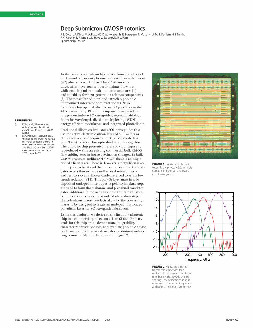
PH.33 MICROSYSTEMS TECHNOLOGY LABORATORIES ANNUAL RESEARCH REPORT 2009 PHotonics
PHotonics
Deep submicron cMos PhotonicsJ. S. Orcutt, A. Khilo, M. A. Popović, C. W. Holzwarth, E. Zgraggen, B. Moss, H. Li, M. S. Dahlem, H. I. Smith, F. X. Kärtner, E. P. Ippen, J. L. Hoyt, V. Stojanović, R. J. Ram Sponsorship: DARPA
In the past decade, silicon has moved from a workbench for low-index contrast photonics to a strong-confinement (SC) photonics workhorse. The SC silicon-core waveguides have been shown to maintain low-loss while enabling micron-scale photonic structures [1] and suitability for next-generation telecom components [2]. The possibility of inter- and intrachip photonic interconnect integrated with traditional CMOS electronics has opened silicon-core SC photonics to the VLSI community. Photonic components required for integration include SC waveguides, resonant add-drop filters for wavelength-division multiplexing (WDM), energy-efficient modulators, and integrated photodiodes.
Traditional silicon-on-insulator (SOI) waveguides that use the active electronic silicon layer of SOI wafers as the waveguide core require a thick buried-oxide layer (2 to 3 µm) to enable low optical-substrate leakage loss. The photonic chip presented here, shown in Figure 1, is produced within an existing commercial bulk CMOS flow, adding zero in-house production changes. In bulk CMOS processes, unlike SOI CMOS, there is no single-crystal silicon layer. There is, however, a polysilicon layer in the process front end that is used to form the transistor gates over a thin oxide as well as local interconnects and resistors over a thicker oxide, referred to as shallow trench isolation (STI). This poly-Si layer must first be deposited undoped since opposite polarity implant steps are used to form the n-channel and p-channel transistor gates. Additionally, the need to create accurate resistors requires a way to block the standard silicidation step of the polysilicon. These two facts allow for the processing masks to be designed to create an undoped, unsilicided polysilicon layer for SC waveguide fabrication.
Using this platform, we designed the first bulk photonic chip in a commercial process on a 4-mm2 die. Primary goals for this chip are to demonstrate integrability, characterize waveguide loss, and evaluate photonic device performance. Preliminary device demonstrations include ring resonator filter banks, shown in Figure 2.
FIGURE 1: Bulk 65-nm photonic test chip die photo. A 2x2 mm2 die contains 116 devices and over 21 cm of waveguide.
-200 0 200 400 600 800 1000
-14
-12
-10
-8
-6
-4
-2
0
Transmission, dB
Frequency, GHz
FIGURE 2: Measured drop-port transmission functions for a 4-channel ring resonator add-drop filter bank with 240 GHz channel spacing. Low process variation is observed in the center frequency and peak transmission uniformity.
REFERENCES[1] F. Xia, et al., “Ultracompact
optical buffers of a silicon chip,” in Nat. Phot. 1, pp. 65-71, (2007).
[2] M.A. Popović, T. Barwicz, et al., “Strong-confinement microring resonator photonic circuits,” in Proc. 20th An. Meet. IEEE Lasers and Electro-Optics Soc. (LEOS), Lake Buena Vista, Florida, Oct 2007, paper TuCC3.
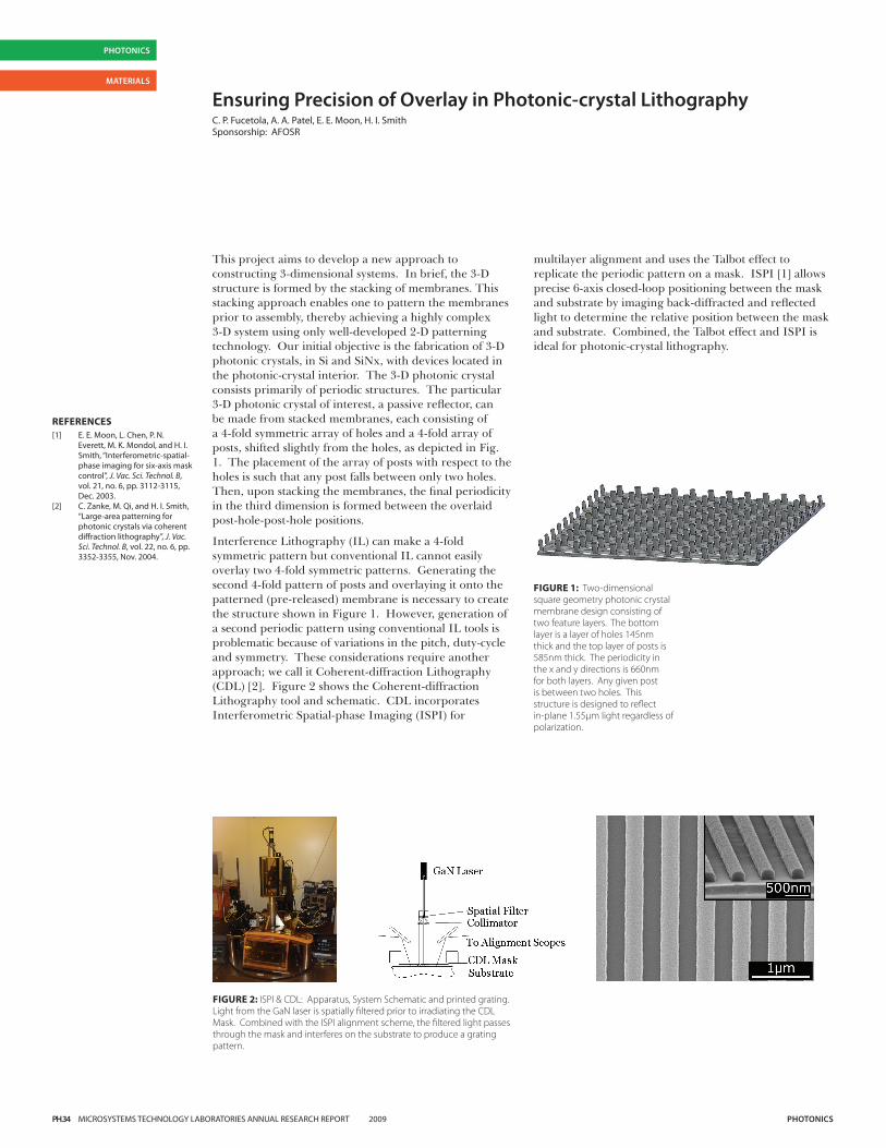
PH.34 MICROSYSTEMS TECHNOLOGY LABORATORIES ANNUAL RESEARCH REPORT 2009 PHotonics
PHotonics
MAtERiALs
Ensuring Precision of overlay in Photonic-crystal LithographyC. P. Fucetola, A. A. Patel, E. E. Moon, H. I. SmithSponsorship: AFOSR
This project aims to develop a new approach to constructing 3-dimensional systems. In brief, the 3-D structure is formed by the stacking of membranes. This stacking approach enables one to pattern the membranes prior to assembly, thereby achieving a highly complex 3-D system using only well-developed 2-D patterning technology. Our initial objective is the fabrication of 3-D photonic crystals, in Si and SiNx, with devices located in the photonic-crystal interior. The 3-D photonic crystal consists primarily of periodic structures. The particular 3-D photonic crystal of interest, a passive reflector, can be made from stacked membranes, each consisting of a 4-fold symmetric array of holes and a 4-fold array of posts, shifted slightly from the holes, as depicted in Fig. 1. The placement of the array of posts with respect to the holes is such that any post falls between only two holes. Then, upon stacking the membranes, the final periodicity in the third dimension is formed between the overlaid post-hole-post-hole positions.
Interference Lithography (IL) can make a 4-fold symmetric pattern but conventional IL cannot easily overlay two 4-fold symmetric patterns. Generating the second 4-fold pattern of posts and overlaying it onto the patterned (pre-released) membrane is necessary to create the structure shown in Figure 1. However, generation of a second periodic pattern using conventional IL tools is problematic because of variations in the pitch, duty-cycle and symmetry. These considerations require another approach; we call it Coherent-diffraction Lithography (CDL) [2]. Figure 2 shows the Coherent-diffraction Lithography tool and schematic. CDL incorporates Interferometric Spatial-phase Imaging (ISPI) for
multilayer alignment and uses the Talbot effect to replicate the periodic pattern on a mask. ISPI [1] allows precise 6-axis closed-loop positioning between the mask and substrate by imaging back-diffracted and reflected light to determine the relative position between the mask and substrate. Combined, the Talbot effect and ISPI is ideal for photonic-crystal lithography.
REFERENCES[1] E. E. Moon, L. Chen, P. N.
Everett, M. K. Mondol, and H. I. Smith, “Interferometric-spatial-phase imaging for six-axis mask control”, J. Vac. Sci. Technol. B, vol. 21, no. 6, pp. 3112-3115, Dec. 2003.
[2] C. Zanke, M. Qi, and H. I. Smith, “Large-area patterning for photonic crystals via coherent diffraction lithography”, J. Vac. Sci. Technol. B, vol. 22, no. 6, pp. 3352-3355, Nov. 2004.
FIGURE 1: Two-dimensional square geometry photonic crystal membrane design consisting of two feature layers. The bottom layer is a layer of holes 145nm thick and the top layer of posts is 585nm thick. The periodicity in the x and y directions is 660nm for both layers. Any given post is between two holes. This structure is designed to reflect in-plane 1.55μm light regardless of polarization.
FIGURE 2: ISPI & CDL: Apparatus, System Schematic and printed grating. Light from the GaN laser is spatially filtered prior to irradiating the CDL Mask. Combined with the ISPI alignment scheme, the filtered light passes through the mask and interferes on the substrate to produce a grating pattern.
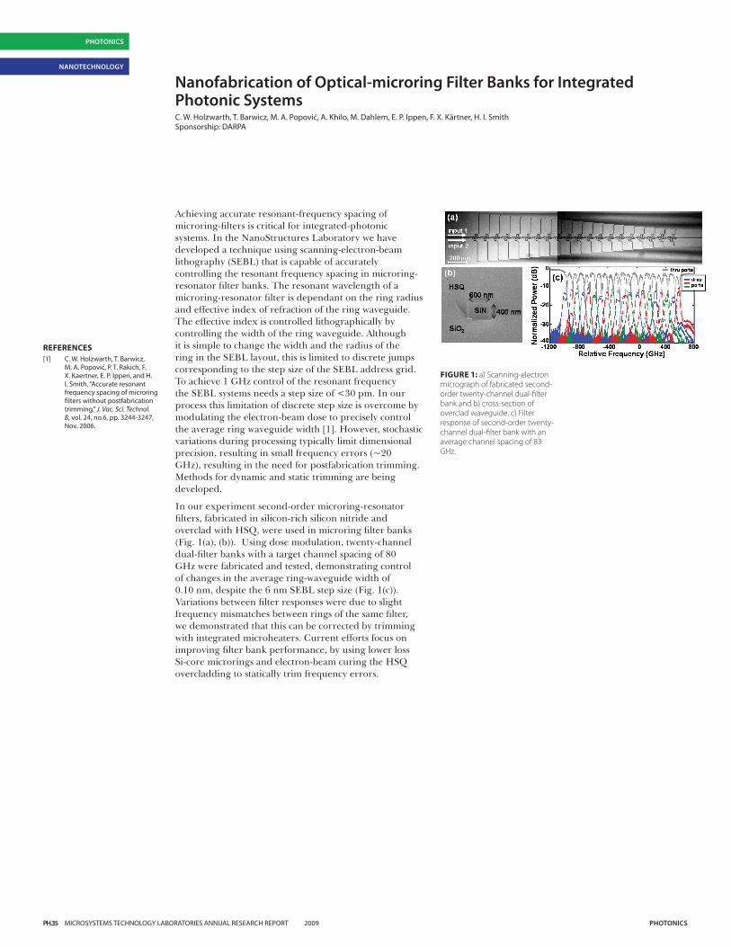
PH.35 MICROSYSTEMS TECHNOLOGY LABORATORIES ANNUAL RESEARCH REPORT 2009 PHotonics
PHotonics
nAnotEcHnoLoGY
nanofabrication of optical-microring Filter Banks for integrated Photonic systemsC. W. Holzwarth, T. Barwicz, M. A. Popović, A. Khilo, M. Dahlem, E. P. Ippen, F. X. Kärtner, H. I. SmithSponsorship: DARPA
Achieving accurate resonant-frequency spacing of microring-filters is critical for integrated-photonic systems. In the NanoStructures Laboratory we have developed a technique using scanning-electron-beam lithography (SEBL) that is capable of accurately controlling the resonant frequency spacing in microring-resonator filter banks. The resonant wavelength of a microring-resonator filter is dependant on the ring radius and effective index of refraction of the ring waveguide. The effective index is controlled lithographically by controlling the width of the ring waveguide. Although it is simple to change the width and the radius of the ring in the SEBL layout, this is limited to discrete jumps corresponding to the step size of the SEBL address grid. To achieve 1 GHz control of the resonant frequency the SEBL systems needs a step size of <30 pm. In our process this limitation of discrete step size is overcome by modulating the electron-beam dose to precisely control the average ring waveguide width [1]. However, stochastic variations during processing typically limit dimensional precision, resulting in small frequency errors (~20 GHz), resulting in the need for postfabrication trimming. Methods for dynamic and static trimming are being developed.
In our experiment second-order microring-resonator filters, fabricated in silicon-rich silicon nitride and overclad with HSQ, were used in microring filter banks (Fig. 1(a), (b)). Using dose modulation, twenty-channel dual-filter banks with a target channel spacing of 80 GHz were fabricated and tested, demonstrating control of changes in the average ring-waveguide width of 0.10 nm, despite the 6 nm SEBL step size (Fig. 1(c)). Variations between filter responses were due to slight frequency mismatches between rings of the same filter, we demonstrated that this can be corrected by trimming with integrated microheaters. Current efforts focus on improving filter bank performance, by using lower loss Si-core microrings and electron-beam curing the HSQ overcladding to statically trim frequency errors.
FIGURE 1: a) Scanning-electron micrograph of fabricated second-order twenty-channel dual-filter bank and b) cross-section of overclad waveguide. c) Filter response of second-order twenty-channel dual-filter bank with an average channel spacing of 83 GHz.
REFERENCES[1] C. W. Holzwarth, T. Barwicz,
M. A. Popović, P. T. Rakich, F. X. Kaertner, E. P. Ippen, and H. I. Smith, “Accurate resonant frequency spacing of microring filters without postfabrication trimming,” J. Vac. Sci. Technol. B, vol. 24, no.6, pp. 3244-3247, Nov. 2006.
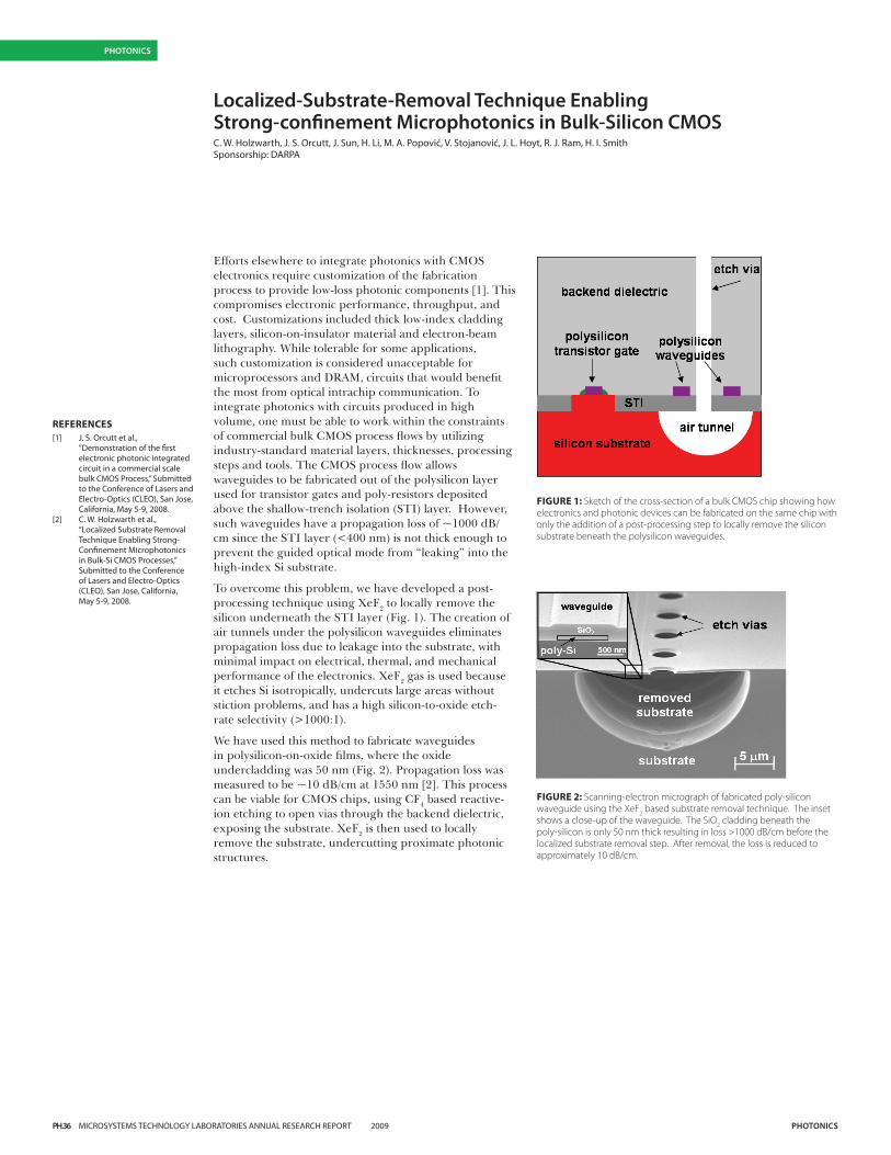
PH.36 MICROSYSTEMS TECHNOLOGY LABORATORIES ANNUAL RESEARCH REPORT 2009 PHotonics
PHotonics
Localized-substrate-Removal technique Enabling strong-confinement Microphotonics in Bulk-silicon cMosC. W. Holzwarth, J. S. Orcutt, J. Sun, H. Li, M. A. Popović, V. Stojanović, J. L. Hoyt, R. J. Ram, H. I. SmithSponsorship: DARPA
Efforts elsewhere to integrate photonics with CMOS electronics require customization of the fabrication process to provide low-loss photonic components [1]. This compromises electronic performance, throughput, and cost. Customizations included thick low-index cladding layers, silicon-on-insulator material and electron-beam lithography. While tolerable for some applications, such customization is considered unacceptable for microprocessors and DRAM, circuits that would benefit the most from optical intrachip communication. To integrate photonics with circuits produced in high volume, one must be able to work within the constraints of commercial bulk CMOS process flows by utilizing industry-standard material layers, thicknesses, processing steps and tools. The CMOS process flow allows waveguides to be fabricated out of the polysilicon layer used for transistor gates and poly-resistors deposited above the shallow-trench isolation (STI) layer. However, such waveguides have a propagation loss of ~1000 dB/cm since the STI layer (<400 nm) is not thick enough to prevent the guided optical mode from “leaking” into the high-index Si substrate.
To overcome this problem, we have developed a post-processing technique using XeF2 to locally remove the silicon underneath the STI layer (Fig. 1). The creation of air tunnels under the polysilicon waveguides eliminates propagation loss due to leakage into the substrate, with minimal impact on electrical, thermal, and mechanical performance of the electronics. XeF2 gas is used because it etches Si isotropically, undercuts large areas without stiction problems, and has a high silicon-to-oxide etch-rate selectivity (>1000:1).
We have used this method to fabricate waveguides in polysilicon-on-oxide films, where the oxide undercladding was 50 nm (Fig. 2). Propagation loss was measured to be ~10 dB/cm at 1550 nm [2]. This process can be viable for CMOS chips, using CF4 based reactive-ion etching to open vias through the backend dielectric, exposing the substrate. XeF2 is then used to locally remove the substrate, undercutting proximate photonic structures.
FIGURE 1: Sketch of the cross-section of a bulk CMOS chip showing how electronics and photonic devices can be fabricated on the same chip with only the addition of a post-processing step to locally remove the silicon substrate beneath the polysilicon waveguides.
FIGURE 2: Scanning-electron micrograph of fabricated poly-silicon waveguide using the XeF2 based substrate removal technique. The inset shows a close-up of the waveguide. The SiO2 cladding beneath the poly-silicon is only 50 nm thick resulting in loss >1000 dB/cm before the localized substrate removal step. After removal, the loss is reduced to approximately 10 dB/cm.
REFERENCES[1] J. S. Orcutt et al.,
“Demonstration of the first electronic photonic integrated circuit in a commercial scale bulk CMOS Process,” Submitted to the Conference of Lasers and Electro-Optics (CLEO), San Jose, California, May 5-9, 2008.
[2] C. W. Holzwarth et al., “Localized Substrate Removal Technique Enabling Strong-Confinement Microphotonics in Bulk-Si CMOS Processes,” Submitted to the Conference of Lasers and Electro-Optics (CLEO), San Jose, California, May 5-9, 2008.
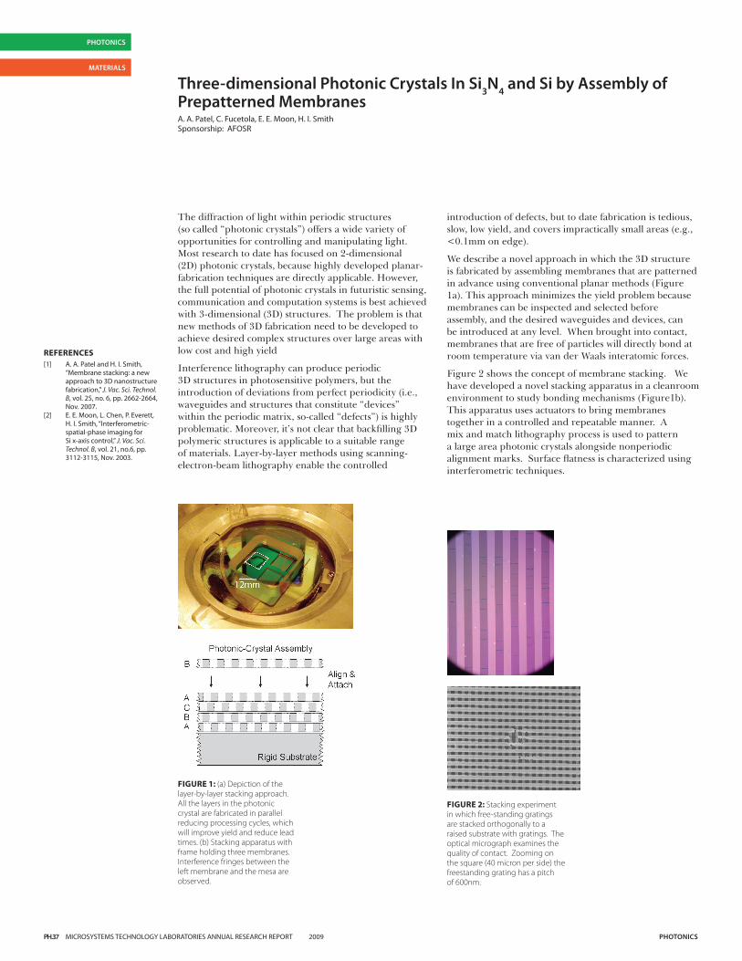
PH.37 MICROSYSTEMS TECHNOLOGY LABORATORIES ANNUAL RESEARCH REPORT 2009 PHotonics
PHotonics
MAtERiALs
three-dimensional Photonic crystals in si3n4 and si by Assembly of Prepatterned MembranesA. A. Patel, C. Fucetola, E. E. Moon, H. I. SmithSponsorship: AFOSR
The diffraction of light within periodic structures (so called “photonic crystals”) offers a wide variety of opportunities for controlling and manipulating light. Most research to date has focused on 2-dimensional (2D) photonic crystals, because highly developed planar-fabrication techniques are directly applicable. However, the full potential of photonic crystals in futuristic sensing, communication and computation systems is best achieved with 3-dimensional (3D) structures. The problem is that new methods of 3D fabrication need to be developed to achieve desired complex structures over large areas with low cost and high yield
Interference lithography can produce periodic 3D structures in photosensitive polymers, but the introduction of deviations from perfect periodicity (i.e., waveguides and structures that constitute “devices” within the periodic matrix, so-called “defects”) is highly problematic. Moreover, it’s not clear that backfilling 3D polymeric structures is applicable to a suitable range of materials. Layer-by-layer methods using scanning-electron-beam lithography enable the controlled
FIGURE 2: Stacking experiment in which free-standing gratings are stacked orthogonally to a raised substrate with gratings. The optical micrograph examines the quality of contact. Zooming on the square (40 micron per side) the freestanding grating has a pitch of 600nm.
FIGURE 1: (a) Depiction of the layer-by-layer stacking approach. All the layers in the photonic crystal are fabricated in parallel reducing processing cycles, which will improve yield and reduce lead times. (b) Stacking apparatus with frame holding three membranes. Interference fringes between the left membrane and the mesa are observed.
REFERENCES[1] A. A. Patel and H. I. Smith,
“Membrane stacking: a new approach to 3D nanostructure fabrication,” J. Vac. Sci. Technol. B, vol. 25, no. 6, pp. 2662-2664, Nov. 2007.
[2] E. E. Moon, L. Chen, P. Everett, H. I. Smith, “Interferometric-spatial-phase imaging for Si x-axis control,” J. Vac. Sci. Technol. B, vol. 21, no.6, pp. 3112-3115, Nov. 2003.
introduction of defects, but to date fabrication is tedious, slow, low yield, and covers impractically small areas (e.g., <0.1mm on edge).
We describe a novel approach in which the 3D structure is fabricated by assembling membranes that are patterned in advance using conventional planar methods (Figure 1a). This approach minimizes the yield problem because membranes can be inspected and selected before assembly, and the desired waveguides and devices, can be introduced at any level. When brought into contact, membranes that are free of particles will directly bond at room temperature via van der Waals interatomic forces.
Figure 2 shows the concept of membrane stacking. We have developed a novel stacking apparatus in a cleanroom environment to study bonding mechanisms (Figure1b). This apparatus uses actuators to bring membranes together in a controlled and repeatable manner. A mix and match lithography process is used to pattern a large area photonic crystals alongside nonperiodic alignment marks. Surface flatness is characterized using interferometric techniques.
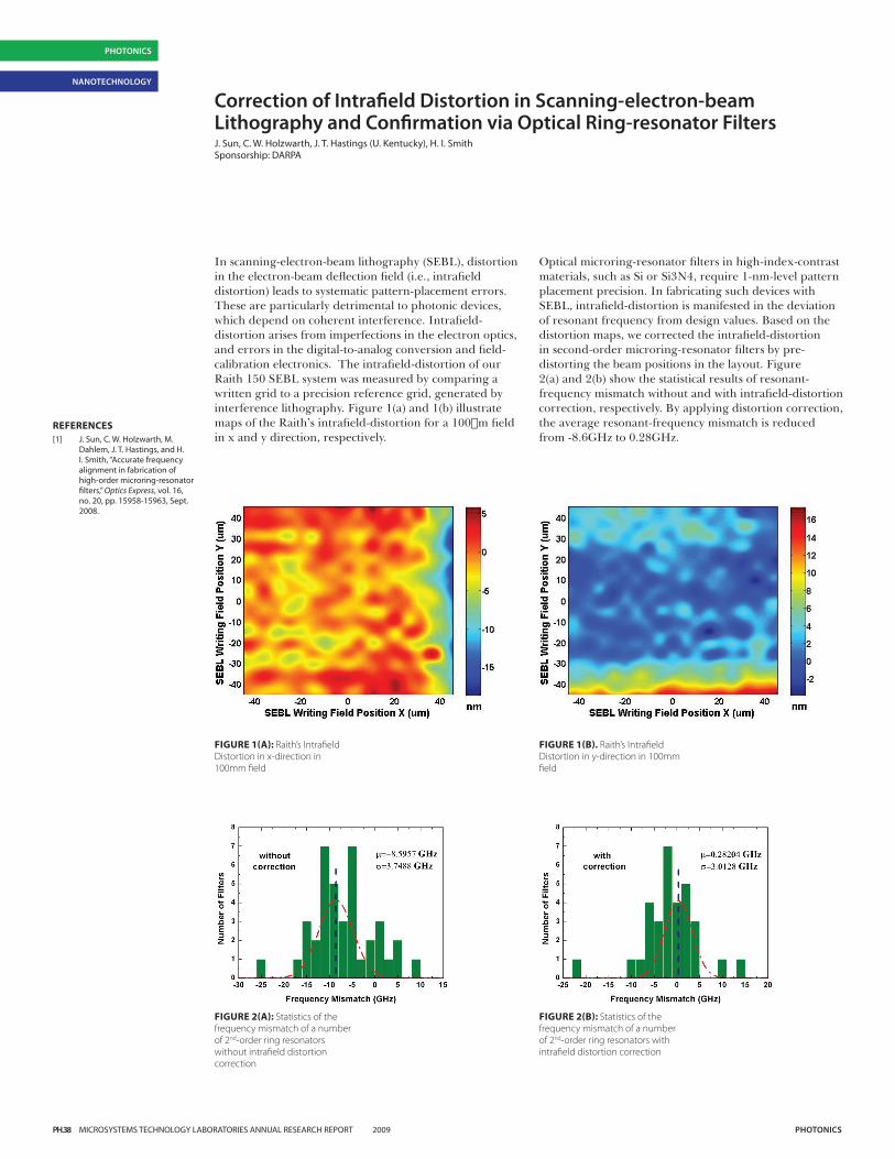
PH.38 MICROSYSTEMS TECHNOLOGY LABORATORIES ANNUAL RESEARCH REPORT 2009 PHotonics
PHotonics
nAnotEcHnoLoGY
correction of intrafield Distortion in scanning-electron-beam Lithography and confirmation via optical Ring-resonator Filters J. Sun, C. W. Holzwarth, J. T. Hastings (U. Kentucky), H. I. Smith Sponsorship: DARPA
In scanning-electron-beam lithography (SEBL), distortion in the electron-beam deflection field (i.e., intrafield distortion) leads to systematic pattern-placement errors. These are particularly detrimental to photonic devices, which depend on coherent interference. Intrafield-distortion arises from imperfections in the electron optics, and errors in the digital-to-analog conversion and field-calibration electronics. The intrafield-distortion of our Raith 150 SEBL system was measured by comparing a written grid to a precision reference grid, generated by interference lithography. Figure 1(a) and 1(b) illustrate maps of the Raith’s intrafield-distortion for a 100m field in x and y direction, respectively.
Optical microring-resonator filters in high-index-contrast materials, such as Si or Si3N4, require 1-nm-level pattern placement precision. In fabricating such devices with SEBL, intrafield-distortion is manifested in the deviation of resonant frequency from design values. Based on the distortion maps, we corrected the intrafield-distortion in second-order microring-resonator filters by pre-distorting the beam positions in the layout. Figure 2(a) and 2(b) show the statistical results of resonant-frequency mismatch without and with intrafield-distortion correction, respectively. By applying distortion correction, the average resonant-frequency mismatch is reduced from -8.6GHz to 0.28GHz.
REFERENCES[1] J. Sun, C. W. Holzwarth, M.
Dahlem, J. T. Hastings, and H. I. Smith, “Accurate frequency alignment in fabrication of high-order microring-resonator filters,” Optics Express, vol. 16, no. 20, pp. 15958-15963, Sept. 2008.
FIGURE 1(A): Raith’s Intrafield Distortion in x-direction in 100mm field
FIGURE 1(B). Raith’s Intrafield Distortion in y-direction in 100mm field
FIGURE 2(A): Statistics of the frequency mismatch of a number of 2nd-order ring resonators without intrafield distortion correction
FIGURE 2(B): Statistics of the frequency mismatch of a number of 2nd-order ring resonators with intrafield distortion correction
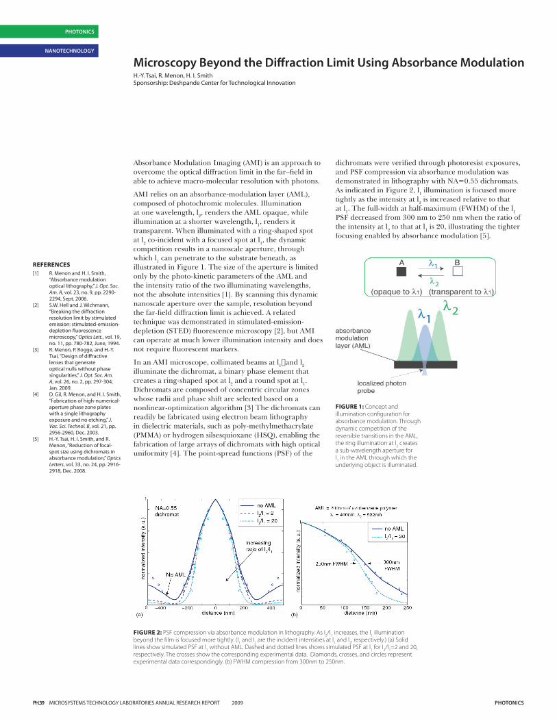
PH.39 MICROSYSTEMS TECHNOLOGY LABORATORIES ANNUAL RESEARCH REPORT 2009 PHotonics
PHotonics
nAnotEcHnoLoGY
Microscopy Beyond the Diffraction Limit Using Absorbance ModulationH.-Y. Tsai, R. Menon, H. I. SmithSponsorship: Deshpande Center for Technological Innovation
Absorbance Modulation Imaging (AMI) is an approach to overcome the optical diffraction limit in the far–field in able to achieve macro-molecular resolution with photons.
AMI relies on an absorbance-modulation layer (AML), composed of photochromic molecules. Illumination at one wavelength, l2, renders the AML opaque, while illumination at a shorter wavelength, l1, renders it transparent. When illuminated with a ring-shaped spot at l2 co-incident with a focused spot at l1, the dynamic competition results in a nanoscale aperture, through which l1 can penetrate to the substrate beneath, as illustrated in Figure 1. The size of the aperture is limited only by the photo-kinetic parameters of the AML and the intensity ratio of the two illuminating wavelengths, not the absolute intensities [1]. By scanning this dynamic nanoscale aperture over the sample, resolution beyond the far-field diffraction limit is achieved. A related technique was demonstrated in stimulated-emission-depletion (STED) fluorescence microscopy [2], but AMI can operate at much lower illumination intensity and does not require fluorescent markers.
In an AMI microscope, collimated beams at l1and l2 illuminate the dichromat, a binary phase element that creates a ring-shaped spot at l2 and a round spot at l1. Dichromats are composed of concentric circular zones whose radii and phase shift are selected based on a nonlinear-optimization algorithm [3] The dichromats can readily be fabricated using electron beam lithography in dielectric materials, such as poly-methylmethacrylate (PMMA) or hydrogen silsesquioxane (HSQ), enabling the fabrication of large arrays of dichromats with high optical uniformity [4]. The point-spread functions (PSF) of the
dichromats were verified through photoresist exposures, and PSF compression via absorbance modulation was demonstrated in lithography with NA=0.55 dichromats. As indicated in Figure 2, l1 illumination is focused more tightly as the intensity at l2 is increased relative to that at l1. The full-width at half-maximum (FWHM) of the l1 PSF decreased from 300 nm to 250 nm when the ratio of the intensity at l2 to that at l1 is 20, illustrating the tighter focusing enabled by absorbance modulation [5].
REFERENCES[1] R. Menon and H. I. Smith,
“Absorbance modulation optical lithography,” J. Opt. Soc. Am. A, vol. 23, no. 9, pp. 2290-2294, Sept. 2006.
[2] S.W. Hell and J. Wichmann, “Breaking the diffraction resolution limit by stimulated emission: stimulated-emission-depletion fluorescence microscopy,” Optics Lett., vol. 19, no. 11, pp. 780-782, June, 1994.
[3] R. Menon, P. Rogge, and H.-Y. Tsai, “Design of diffractive lenses that generate optical nulls without phase singularities,” J. Opt. Soc. Am. A, vol. 26, no. 2, pp. 297-304, Jan. 2009.
[4] D. Gil, R. Menon, and H. I. Smith, “Fabrication of high-numerical-aperture phase zone plates with a single lithography exposure and no etching,” J. Vac. Sci. Technol. B, vol. 21, pp. 2956-2960, Dec. 2003.
[5] H.-Y. Tsai, H. I. Smith, and R. Menon, “Reduction of focal-spot size using dichromats in absorbance modulation,” Optics Letters, vol. 33, no. 24, pp. 2916-2918, Dec. 2008.
FIGURE 2: PSF compression via absorbance modulation in lithography. As I2/I1 increases, the l1 illumination beyond the film is focused more tightly. (I1 and I2 are the incident intensities at l1 and l2, respectively.) (a) Solid lines show simulated PSF at l1 without AML. Dashed and dotted lines shows simulated PSF at l1 for I2/I1=2 and 20, respectively. The crosses show the corresponding experimental data. Diamonds, crosses, and circles represent experimental data correspondingly. (b) FWHM compression from 300nm to 250nm.
FIGURE 1: Concept and illumination configuration for absorbance modulation. Through dynamic competition of the reversible transitions in the AML, the ring illumination at l2 creates a sub-wavelength aperture for l1 in the AML through which the underlying object is illuminated.