Embed Size (px)
Citation preview
PHILIPS
PHILIPS Electronic components and materials
Technical note 064
Digital cassette interface fora 2650 microprocessor system
The digital cassette recorder offers many attractive facilities to the microcomputer user: its large storage capacity (0,5 Mbyte) and high data I/O rate are far superior to either punched cards or paper tape. Moreover, its sturdy construction and small size make it an excellent medium for data storage and transport. In use, the digital cassette recorder is quiet, reliable and simple to operate.
This publication describes an interface between the Philips Digital Cassette Drive (DCR) and a 2650-based microcomputer system. Data transfer is performed under interrupt program control in order to prevent undue wastage of processing time. The data format on the cassettes complies with the ECMA* standards 34 and 41 for BASIC labelled cassettes.
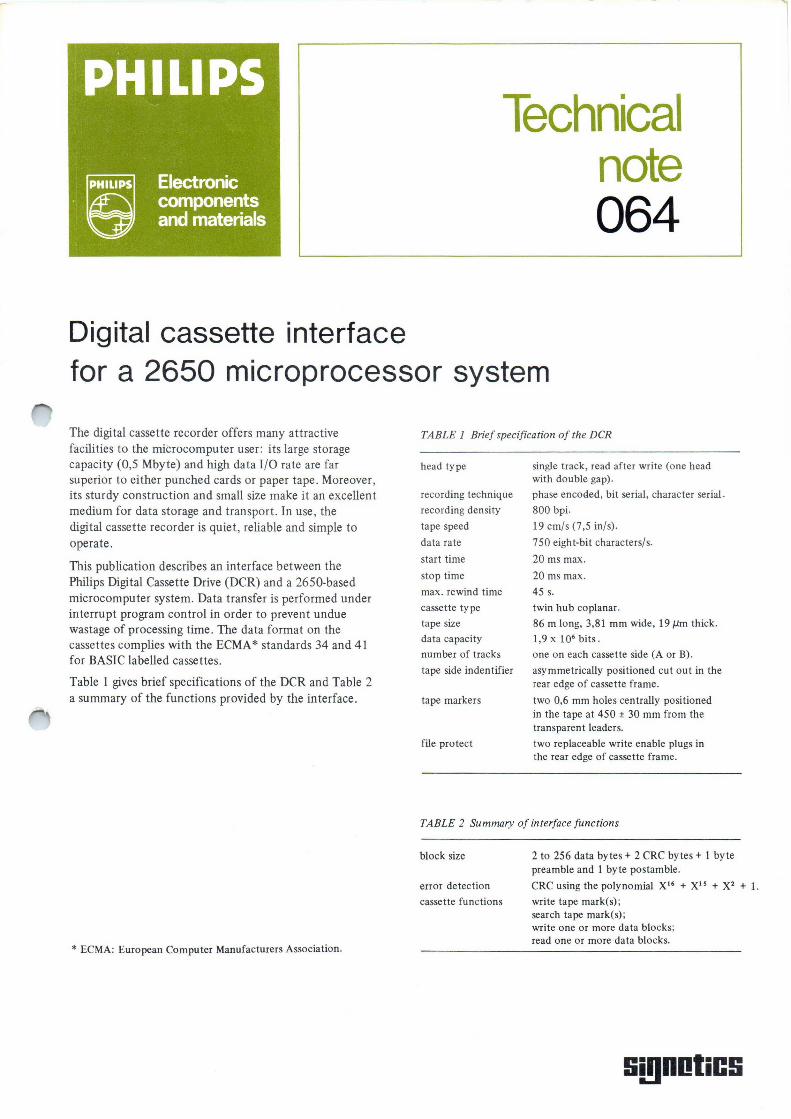
Table 1 gives brief specifications of the DCR and Table 2 a summary of the functions provided by the interface.
* ECMA: European Computer Manufacturers Association.
TABLE 1 Brief specification of the DCR
head type
recording technique
recording density
tape speed
data rate
start time
stop time
max. rewind time
cassette type
tape size
data capacity
number of tracks
tape side indentifier
tape markers
file protect
single track, read after write (one head with double gap).
phase encoded, bit serial, character serial.
800 bpi.
19 cm/s (7,5 in/s).
750 eight-bit characters/s.
20 ms max.
20 ms max.
45 s.
twin hub coplanar.
86 m long, 3,81 mm wide, 19µm thick.
1,9 x 106 bits.
one on each cassette side (A or B).
asymmetrically positioned cut out in the rear edge of cassette frame.
two 0,6 mm holes centrally positioned in the tape at 450 ± 30 mm from the transparent leaders.
two replaceable write enable plugs in the rear edge of cassette frame.
TABLE 2 Summary of interface functions
block size
error detection
cassette functions
2 to 256 data bytes + 2 CRC bytes + 1 byte
preamble and 1 byte postamble.
CRC using the polynomial X16 + X' S + XZ + 1.
write tape mark(s); search tape mark(s); write one or more data blocks; read one or more data blocks.
S'~JI IIL~tiCs
Cassette data format
Data is recorded on the cassette in a single track, serial mode in blocks of 8-bit bytes. The least significant bit of a byte is written and read first. By turning the cassette onto its other side, a second track is available, recorded in the reverse direction. The DCR can distinguish between side A and side B by sensing an asymmetrical slot in the cassette.
For recognition and synchronization purposes, the data in a block is preceded by a preamble character and followed by two CRC* bytes and a postamble character. The preamble and postamble characters are each a single byte with the hexadecimal value `AA' (binary pattern 10101010).
Tape marks are used to define the beginning-of-file, end-of-records and end-of-file. A tape mark consists of a preamble character, two bytes of all zeros and a postamble character.
Tape marks and data blocks are all separated by a gap corresponding to at least 100 ms at the nominal transport speed.
A data block may contain from 2 to 256 data bytes; this interface has been designed to write a variable length block in this range as specified by the user's write command. When requested to write more than 256 data bytes, the interface directs the DCR to write a variable length block followed by a number of blocks each of 256 data bytes. The interface allows from 1 to 256 data blocks to be read or written from one command.
Recording technique
The DCR uses the well-known phase-encoding technique in which a data bit is recorded as a change in the magnetic flux of the tape. Azero is recorded as a flux transition from a north pole to a south pole, and a one as a flux transition from a south pole to a north pole. This method of encoding allows a high bit-density on the tape.
When two or more consecutive ones or zeros are to be written, additional flux changes are required between the bit flux changes. These phase flux changes occur at the nominal mid-point between the bit flux changes. Figure 1 shows the relationship between the data to be recorded and the bit and phase flux changes.
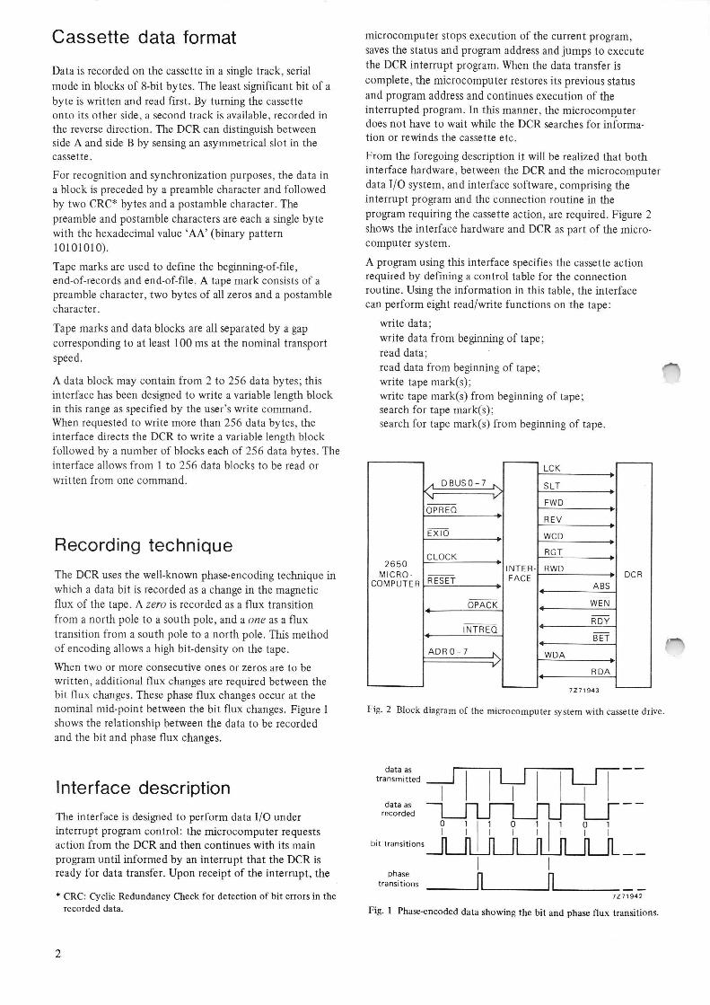
Interface description The interface is designed to perform data I/O under interrupt program control: the microcomputer requests action from the DCR and then continues with its main program until informed by an interrupt that the DCR is ready for data transfer. Upon receipt of the interrupt, the
* CRC: Cyclic Redundancy Check for detection of bit errors in the recorded data. Fig. 1 Phase-encoded data showing the bit and phase flux transitions.
microcomputer stops execution of the current program, saves the status and program address and jumps to execute the DCR interrupt program. When the data transfer is complete, the microcomputer restores its previous status and program address and continues execution of the interrupted program. In this manner, the microcomputer does not have to wait while the DCR searches for informa-tion or rewinds the cassette etc.
From the foregoing description it will be realized that both interface hardware, between the DCR and the microcomputer data I/O system, and interface software, comprising the interrupt program and the connection routine in the program requiring the cassette action, are required. Figure 2 shows the interface hardware and DCR as part of the micro-computer system.
A program using this interface specifies the cassette action required by defining a control table for the connection routine. Using the information in this table, the interface can perform eight read/write functions on the tape:
write data; write data from beginning of tape; read data; read data from beginning of tape; write tape mark(s); write tape marks) from beginning of tape; search for tape mark(s); search for tape marks) from beginning of tape.
DBUSO-7
LCK
SLT
FWD OPREO
REV
EXIO WCD
CLOCK RGT
RWD 2650 INTER- MICRO-
COMPUTER FACE DCR
RESET ABS
OPACK WEN
RDY INTREO
BET a WDA ADRO-7
RDA
7271943
Fig. 2 Block diagram of the microcomputer system with cassette drive.
data as transmitted
data as recorded
0
bit transitions r
phase transitions
0 I
rnisaz
2

Interface hardware TABLE 4 Signals between DCR and interface
This is comprised of 27 TTL integrated circuits. Figure 3 shows the schematic diagram of the cassette interface hardware. Table 3 lists the signals to and from the micro-computer while Table 4 lists those to and from the DCR.
TABLE 3 Signals between microcomputer and interface
signal function
OPREQ operation request from microcomputer, active LOW.
OPACK operation acknowledge from interface, active LOW.
INTREQ interrupt request from interface, active LOW.
EXIO extended I/O signal from the microcomputer instructing the interface to compare its address with the data on the address bus. It is an active LOW signal, formed by the combination:
DBUSO-7 8-bit bidirectional data bus.
ADRO-7 8-bit command/peripheral number bus.
CLOCK nominal 1 MHz clock from microcomputer.
RESET general system reset signal, active LOW.
M/ 10•E/NE
CLOCK
R
RESET DBUSO-7
i R
READ
SHIFT REGISTER
INTREQ
DATA BUFFER
signal function
control lines
LCK locks the cassette retrieval bar in position and lights the LOCK lamp.
SLT selects the DCR —enables cassette action.
FWD forward, causes the tape to move forwards at capstan speed.
REV reverse, causes tape to move in the reverse direction at capstan speed.
WCD write command, enables the write logic.
RGT read gate, enables the read logic.
RWD rewind the tape at hub speed.
status lines
ABS A or B side of cassette, LOW when A side in use (on top).
WEN write enabled, active LOW, indicates that the write enable plug is present for the side in use.
RDY ready, active LOW, indicates that the tape has been positioned and the LCK and SLT lines are active.
BET Beginning-or-End-of-Tape, active LOW, indicates that the BOT or EOT marker (hole in tape) or transparent leader has been detected by the photocell.
data lines
WDA write data, serial, phase~ncoded data to be recorded. RDA read data, serial, phase-encoded data read from the tape.
OPREO
OPACK EXIO ~ ADRO-7 I
ABS
i
WEN
STATUS COMPARATOR ay 5
OPERATION CONNECTION WORD BUFFER FLIP-FLOP
DECODER
~ 8
READ
CLOCK
WRITE CLOCK
.~ 8
WRITE SHIFT
REGISTER
ERASE
FLIP-FLOP
FORWARD
FLIP-FLOP
.READY
GATE
READ/WRITE COUNTER
R
CALL
FLIP-FLOP
~~ R
R
•—~, REVERSE
FLIP-f LOP
REWIND FLIP-FLOP
SLT ~ LCK
RDY
• FWD
• RWD
R
R
PHASE ENCODER
READ GATE FLIP-FLOP
WRITE COMMAND FLIP-FLOP
]Z]195)
Fig. 3 Block diagram of the interface hardware.
BET
~ REV
• WCD
~ RGT
~ WOA
• RDA
3

Address bus Exlo
~cc The least significant eight bits of the microcomputer address bus are used for peripheral selection when the signal M/I~ indicates I/O action. ADRO to ADR4 are used as a peripheral address, the peripheral responding when the data on these lines coincides with its own hard-wired address. ADRS to ADR7 are used to command the interface, the commands are listed in Table 5. Figure 4 shows the peripheral address and command decoding logic.
TABLES Commands to the interface
mnemonic command ADR7 ADR6 ADRS
STAT status request 1 0 1
CX connection 0 1
OEC output exchange 1 0 0
IEC input exchange 0 0 1
DX disconnection 1 1 1
Data bus
Data from the microcomputer, on the data bus, is clocked into the peripheral register during the Output Exchange Command (OEC) and transferred to the write circuit. During an Input Exchange Command (IEC), the data that has been read from the tape is transferred to the data bus.
Status and control logic
Before commencing data transfer, the microcomputer must establish that the DCR is ready for such an action. The status request command to the peripheral asks for the status word, the value of which describes the condition of the peripheral. The information conveyed by the status word is given in Table 6.
TABLE 6 Status words
bit function
0 ABS signal: 0, side A; 1, side B.
1 WEN, write enable signal, 0: write enabled.
2 not used.
3 not used.
4 RDY, ready signal.
5 not used.
6 GAPS signal, indicates no data on tape, gap between tape marks and/or data blocks.
7 BET signal, 0: marker indicating Beginning-or-End-of-Tape sensed.
-0 ~ BqI `_°~ .6 B
~' -
~o 3
~ ~ 62
~4 B, I s3za
-- ~.3
~---o ADRO
9 Aq
ADRi
ADR2
ADR3
ADR4
OPREO
11
1
13
B
A>B
A<B
A3
A2 A=6
Ai
AO
OPACK --0<
740\4 RESET
ADRS
ADR6
ADR7
4 5 6
V
~5
V
VZ
V
74 LS136
not used
RESET 1
ACC
~cc —
DX
DX
7404 STAT
C
7474
D O
S
4
STAT
11 7404 OEC
OEC
13 7404
11 ̂
CX
'--I ~ CX
14* 7404 IEC
D-- IEC
7aoa
S LT, LCK Ito DCR 1
]Z)1950
Fig. 4 Address and command decoding logic.
Once the microcomputer has ascertained the status of the DCR, it issues a Connection Command (CX) and outputs anoperation word to the data bus. When the interface recognizes the connection command, the operation word on the data bus is clocked into the operation word buffer. Each bit of the operation word, apart from bit 3 which is not used, corresponds to a particular sigrial within the interface:
bit 0 A signal, which sets the Read Gate (RGT) flip-flop to enable reading after the start-reading delay (20 ms) is finished. The RGT flip-flop is reset either by the reset signal or by a disconnection command.
bit 1 B signal, which sets the CALL flip-flop. The not-true output of the CALL flip-flop is the signal INTREQ. The flip-flop is reset either by the reset signal or by a disconnection or exchange command.
bit 2 C signal, which sets the Write Command (WCD) flip-flop to enable writing after the start-writing delay (60 ms) is finished. The flip-flop is reset either by the reset signal or by a disconnection command.
4

bit 3 Not used.
bit 4 E signal, which sets the ERASE and WCD flip-flops. The not-true output of the ERASE flip-flop is used to set the WDA flip-flop so that the data line does not convey data during the erase function.
bit 5 F signal, which sets the Forward (FWD) flip-flop. It is reset by the reset signal or a disconnection command.
D BUSO
D BUS1
D BUS2
D BUSS
D BUS4
D BUSS
D BUS6
D BUST
CX
~1 15
3
6
13
10
3
8728
4
2 7 5 12
operation status word word
I
~ ABS
~ WEN
►A
►B
14 8
►C
6
13
10
8728
4 27
►p
~ READV
►E
5 12 14 8
F
►G
VCC
VCC
RGT
11
1 I15
►H
D C
S 7474 R O O
A CX
D c $ 7474 R
O
1 CX
GAPS
STAT
BET
C
7404 RDY
FWD
74 LS11 1 RWD
)Z)t95t
REWIND FLIP-FLOP
READ GATE FLIP-FLOP
D C VCC S 7474 R
Q
~EFF
ERASE FLIP-FLOP
>Z)1905
bit 6 G signal, which sets the Reverse (RED flip-flop. It is reset by the reset signal or a disconnection command.
bit 7 H signal sets the Rewind (RWD) flip-flop. The rewind flip-flop is reset either by the reset signal or by the signal BET (not Beginning-or-End-of-Tape).
The bidirectional operation/status word register and the associated control flip-flops are shown in Fig. 5.
( from DCR I
VCC
7432 CX
CX
D C S 7474 R
O
R V
K
CX
D C
S 7474 VCC R O O
i I FWD FWD
BECHX EO FIN
7427
Fig. 5 Operation/status word register and logic.
7408
WRITE COMMAND F LIP-FLOP
REVERSE FLIP-FLOP
FORWARD FLIP-FLOP
)Z)19a~
DX
CALL FLI P~F LOP
)Z )~9~6
5

Write logic
The write logic consists of the write clock, write/read counter, write shift register, phase encoder and WCD flip-flop. The write logic is activated when the micro-computer has issued the appropriate connection command followed by an output exchange command with the data to be written. During the output exchange command, the data is transferred via the data buffer to the write shift register. The data path can be seen in Fig. 3 and the timing sequence is shown in Fig. 6.
The circuit of the write clock is shown in Fig. 7; it comprises two decade counters to derive the 12 kHz square-wave from the 1 MHz clock from the micro-computer.
The write/read counter, Fig. 8, is used to count cycles of the write clock waveform corresponding to the eight bits of a character. The output QA is used to shift each of the data bits serially out of the shift register, the BECHX signal being generated by the carry output at the end of a character.
connection routine interrupt routine
value of control counter
DX
ZERO ONE TWO FOUR FIVE SIX
The write data circuit is shown in Fig. 9. The data is converted from parallel to serial format by the register and then phase encoded by the exclusive-OR gate. The QA signal to the exclusive-OR gate provides the phase flux transitions when these are required. The output of the phase encoder is stored in the WDA (write data) flip-flop for a period determined by the WCP (write clock pulse) signal. The EFF signal from the ERASE flip-flop is connected to the set input of the WDA flip-flop so that the data line remains HIGH during erasing.
At the end of each character, the BECHX signal allows the write register to be loaded with the next character from the data buffer. The BECHX signal also causes the CALL flip-flop to be set, in order to receive the next character (command) from the microcomputer.
ONE TWO FOUR FIVE SIX
CX ~~~~
F SIGNAL n ,~
FWD r—'~~ FLIP-FLOP _j
B SIGNAL
CALL FLIP-FLOP (INTREO) ..
E SIGNAL ~~
ERASE ~ I I FLIP-FLOP 175
~~m—s -► 60 ms
OEC
C SIGNAL
6
l
f '~ 100ms
gap ~~
100ms
I gapI
40 ~ ms
00 post-amble
00
WCD ~ FLIP-FLOP
BECHX
OA
WDA
I ~ ~
pre- .. amble
//
!/
00 00 post -amble
00
//
pre amble
//
// 1
Fig. 6 Timing sequence for writing.
// ]Z]195fi
6

uCC
CLOCK
micro-computer
Nock pulses I1 MH 1
VC
uCC
110 ~15 Dp DC Dg DA
11
LOAD
74192 CLEAR DOWN
BORROW CARRY DD DC DB OA
ACC
3 12 I7 I6 (2 I3
9 11011 115
not used
17 Dp DC Dg DA LOAD UP
74192 CLEAR DOWN
BORROW CAfl RV Dp DC DB Oq
13 112 7 6 I2 3
' ~. not used
7432 7432
4
R ESETa RESET C•
7404
83µs ~~
wcP J L (write clock pulse) ~~ ~~
43µs
Fig. 7 Write clock circuit.
)Z)195Z
'/
/O~\
`I74D4
BE CIHX
667 BB6 665 864 883 B62 8B1 BBO
111 112 113 114 I3 I4 I5 I6 A B C D E F G H LOAD CLOCK CLOCK
SHIFT REGISTER 74165 INHIBIT SE RIAL INPUT DH
OA
110 7
woA ( data m DCR 1
Fig. 9 Write data circuit.
Dp DC Dg DA LOAD
CLOCK 74161 CLEAR
CARRY
T P OC Og OA
Fig. 8 Write/read counter.
15~
RESET
)Z)t9aZ
7271953
7

Read logic
The read logic comprises the read clock, read shift register, write/read counter and read gate flip-flop.
The read clock acts as a discriminator between the bit flux transitions and the phase flux transitions in the data signal from the DCR. Both preamble and postamble characters possess only bit flux transitions, so that the read clock, which is a monostable, can be synchronized to these and then mask out the phase flux transitions in the data signal. The phase flux transitions occur midway between bit flux transitions and the monostable remains set for 130 µsin a period of 166 µs. The circuit of the read clock is shown in Fig. 10.
CX
F SIGNAL
FORWARD
~RDAI
(data from DCR I
7aoa
7404
7404
7404
7486
RCP read uCC
clock pulses
14
Fig. 10 Read clock circuit.
connection routine interrupt routine
RDA
In the read mode, the write/read counter counts the bit flux transition pulses and sets the EQFIN signal at the end of a byte (eight pulses). The EQFIN signal enables the three-state outputs of the read register and sets the CALL flip-flop to inform the microcomputer that the data is ready for transfer.
The read data circuit is shown in Fig. 11. The phase-encoded output from the DCR is shifted through the register, clocked by the read clock to ensure that only data is accepted. When the byte is complete, the EQFIN signal enables the three-state data buffer to accept the data from the paralleloutputs of the shift register. The timing sequence for reading is shown in Fig. 12.
1 RDA
RGT 2
RCP
IB RESET
I9CLOCK CLEAR
SERIAL INPUT SHIFT REGISTER
INPUT 74164 ENABLE
GA Dg OC Op OE OF OG OH
3 4 5 6 10 12 13
2 4 6 10 12 14 12 14
i 4]nF
15 8T97 8 T97 15
75 kSt
EQFI/NR\
3 I5 7 I9 11 I73 11 I13
886 B64 882 880
BB7 665 683 BB1
]n 19se
value of control counter ZERO ONE TWO/THREE FOUR
~~
EQFIN
Fig. 11 Read data circuit.
ZERO ONE
]2]1969
TWO FOUR
FLIP-FLOP
~~20 mss
A SIGNAL I I
READ GATE FLIP FLOP
RDA
EQFIN
CALL FLIP FLOP
IEC
DX
GAPS
/~
ot o l ol o l 0000000a00000aoaol ol ol
~ ~ t ot olot 000000000000000001 0]0l
(/
Fig. 12 Timing sequence for reading.
]Z]1959
8
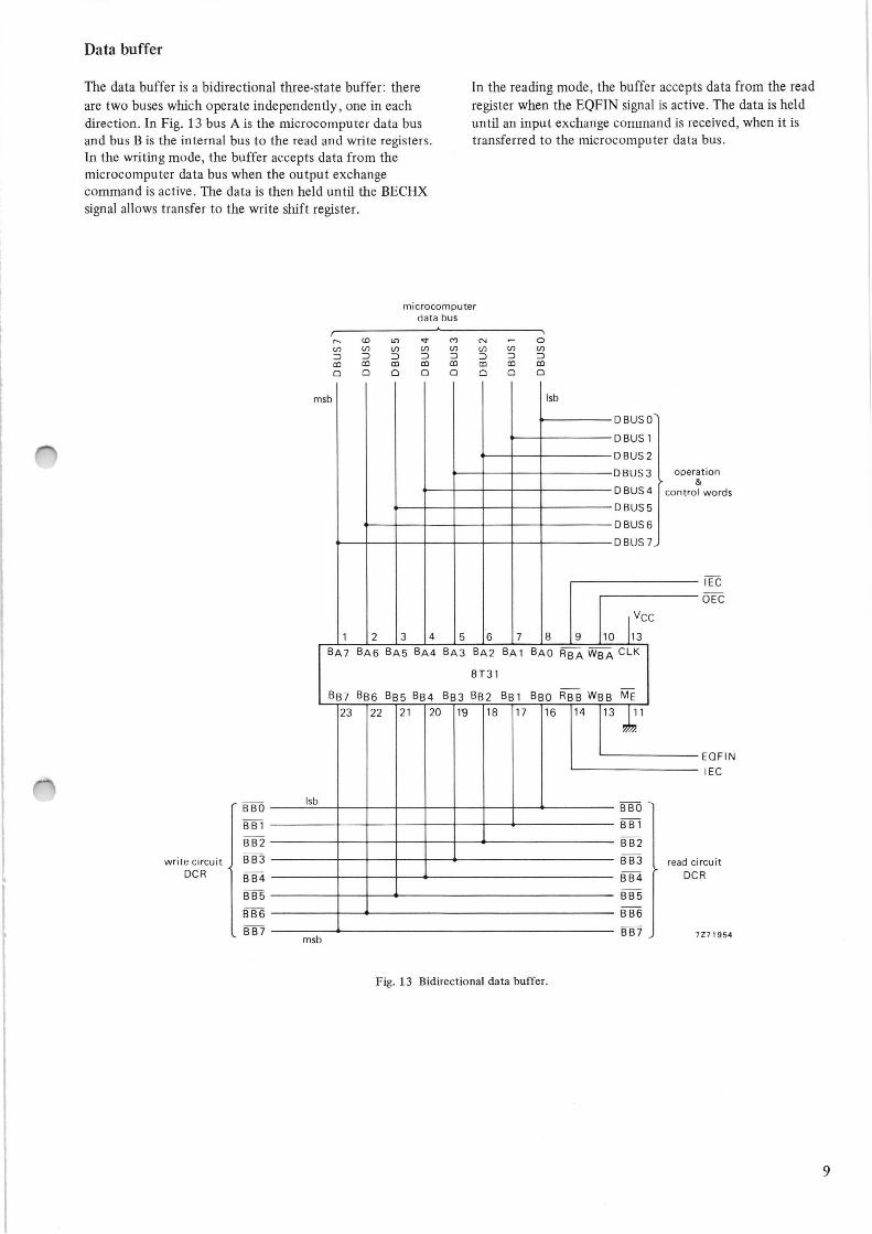
Data buffer
The data buffer is a bidirectional three-state buffer: there are two buses which operate independently, one in each direction. In Fig. 13 bus A is the microcomputer data bus and bus B is the internal bus to the read and write registers. In the writing mode, the buffer accepts data from the microcomputer data bus when the output exchange command is active. The data is then held until the BECHX signal allows transfer to the write shift register.
write circuit DCR
msb
Isb
In the reading mode, the buffer accepts data from the read register when the EQFIN signal is active. The data is held until an input exchange command is received, when it is transferred to the microcomputer data bus.
microcomputer data bus
N
00
V)
a0 O
v U7
m O
M N
00
N
m ra
O V)
¢7
Isb
1 2 3 4 5 6 7 8
DBUSO~
DBUS1
DBUS2
DBUS3
DBUS4
DBUS5
DBUS6
D BUS 7,
9 10 ~13
ACC
6A7 6A6 6A5 6A4 6A3 6A2 6A1 BAO Rgq WgA CLK
8T31
6B7 666 6B5 664 683 6B2 661 BBO RBB WBB ME
23 22 21 20 15 18 17 16 14
msb
Fig. 13 Bidirectional data buffer.
BBO
BB1
BB2
663
664
BB5
686
B67
operation > &
control words
IEC
OEC
EOFIN IEC
read circuit DCR
7277954
9

Interface software
The software can communicate with the peripheral using the two 2-byte I/O instructions READ EXTENDED (REDE) and WRITE EXTENDED (WRTE). The second byte of these instructions is presented on the address bus as the peripheral address and the command. Table 5 shows the five peripheral commands available. The software is comprised of two parts: the connection routine and the interrupt program.
START
LOAD ADDRESS OF CONTROL TABLE
INTO R 0, R 1
STORE REGISTER IN RET,RET+1
MOVE CONTROL TABLE TO CML—CML+5
CLEAR CRC LOCATIONS
ISSUE STAT & RECEIVE
STATUS WORD
CCXR
TROP
CSTR
YES
YES
YES
FORWARD
DELAY 7,Qs
ISSUE STAT & RECEIVE
STATUS WORD
Fig. 14 Flow chart of the connection routine.
YES
SFC2
LOP
STR
YES
The connection routine is part of the main program in order to conserve space in the return address stack. Its function is to transfer the control table, specifying the cassette action that is required, to the cassette memory locations CML to CML+S, check the DCR status and issue a connection command if the status is correct; Fig. 14.
The interrupt program is entered each time the micro-computer receives an interrupt request from the CALL flip-flop. This program uses the control table to define its action, in conjunction with the control counter, which is incremented after each phase of the required operation. It is this program that controls the input/output of data, as specified by the control block. Each entry into the interrupt program will result in a transfer of one byte to or from the microcomputer.
The flow chart of the interrupt program is shown in Fig. 15.
FORWARD
START READING DELAY, 20 ms
RESET ERASE &WCD
SET RGT& FWD
SET CALL, FWD,ERASE,
WCD, BISTAB LES
YES
SET ERASE, FWD& WCD
DE LAV 175 ms
O
LOAD R3 WITH OPERAND TABLE LENGTH
RETURN TO MAIN PROGRAM
AT ADDRESS GIVEN BY R0, R1 MODIE IED
BV R3
SPE
CIAL
>Z)i960
IO

ENTER
SAVE R 0 & PSL IN LOC, LOC+7
SELECT REG BANK 1
VES
SEND IEC b RECEIVE BYTE
SEND OEC b POSTAMBLE
DE LAV 150Ns
CONTROL COUNTER =6?
N
CONTROL COUNTER =0?
CONTROL COUNTER =1?
YES
VES
NO C RCM
CONTROL COUNTER =2?
CONTROL COUNTER .3?
CONTROL COUNTER
SECH YES
SEND OEC b H'AA' DATA
O
ERA
SET ERASE, FWD a WCD BISTABLES RESET CALL FF
SEND OEC 6 H'AA' BYTE
DE LAV 100 ms FOR GAP
DECREMENT DATA BLOCK COUNTER
SET CONTROL COUNTER TO 1
SET WCD, FWD & R SET
ERASE GIST ABLE
O
O
SEND OEC & CRC BYTE
SEND IEC RECEIVE ls~ eVTE
DATA?
INCREMENT CONTROL COUNTER
SEND OEC d H'00'BVTE
R ESET FWD SET ERASE, WCD
BISTABLES
VES
VES
YES
SEND IEC & RECEIVE BYTE
BYTE _ H'00' ?
iSEND OEC
& PREAMBLE
SET TEMP FLAG
fl ESET CONTROL COUNTER
DM
DECREMENT TAPE MARK COUNTER
RESET RGT 50 ms
DISC
DISCONNECT COMMAND
DELAY 40 ms STOP FORWARDSI
DISCONNECTION COMMAND
FIN
i2>>96~
OE LAV 60 ms RESET ERASE, SET FWD, WCD
BISTABLES
AL
IS TEMP FLAG SET >
Fig. 15 Flow chart of the interrupt program.
N
READ ?
VES
FDB
SU BROUTINE CRC &INCREMENT
ADDRESS COUNTER
DECREMENT BYTE COUNTER
BYTE COUNTER
0?
RESTORE R0, PSL d
REG BANKO
150 Ps DE LAV
VES
C RETURN TO 1 MAIN PROGRAM)
VES
SEND IEC d RECEIVE DATA BYTE
INCREMENT CONTROL COUNTER
RERE
CLEAR TEMP FLAG RESET RGT 50 ms
NEW
V ES
DELAY 150ys
YES
SU BROUTINE CRC &INCREMENT
ADDRESS COUNTER CALL
11

Cassette operation sequence
Data exchange with the DCR is initiated by entry into the connection routine: this stores the continuation address of the main program and transfers the control table into the locations CML to CML+S for use by the interrupt routine. Figure 14 shows the flow chart of the connection routine.
The information in the control table is shown in Table 7, with the operands that must be defined for a particular function in Table 8.
TABLE 7 Contents of the control table
operand byte function
1 1 control word: bit 0 ~ (three-bit control counter bit 1 !l used by interrupt routine. bit 2 Must initially be zeros. bit 3 bit 4
bit 5
bit 6
bit 7
not used. 1 indicates read/write from BOT. CRC error flag. 1 if error detected. data/tape mark indicator, 1 indicates tape mark. read/write select, 1 indicates write.
2 2 number of bytes in the first block to be written.
3 3 number of tape marks to be read/written.
4 4 number of data blocks to be read/written.
5 5} 6 address of the first byte to be read/written.
TABLE 8 Specification of control word and operands
control function
word operands to be specified
H`80' write data H`90' write data from beginning of tape
H`00' read data
H`10' read data from beginning of tape
H`CO' write tape marks H`DO' write tape marks from beginning of tape H`40' read tape mazks H`50' read tape marks from beginning of tape
2,4,5
2,4,5
4,5
4,5 3 3 3 3
After requesting the DCR status and, if necessary, waiting until this is correct, the connection routine issues a connection command accompanied by an operation word to start the required cassette action, e.g. rewind to beginning of tape. When the tape has been positioned as required, the connection routine takes into account any delays, e.g. start-reading delay, and issues another connection command. The operation word will be set to enable reading or writing and in the case of writing, the CALL flip-flop will be set, enabling the interface to ask for the first byte of write data. In the reading mode, the CALL flip-flop will be set by the end-of-character signal EQFIN, informing the microcomputer that the requested data is available. Setting the CALL flip-flop results in the signal INTREQ, causing entry to the interrupt program to perform the data transfer.
After performing the above actions, the connection routine forms a branch indexed absolute instruction to the address following the control table, to continue execution of the main program.
The microcomputer will enter the interrupt program after receiving an interrupt request from the interface hardware. In this, the first action is to save the contents of RO and the PSL in locations LOC and LOC+1.
Further actions of the interrupt program depend on the value of the control counter, held in the least significant three bits of the control word. The control counter is initially zero.
Counter = 0
Writing mode: the microcomputer sends an OEC and a preamble character. It then goes to the start-writing delay subroutine (60 ms) before resetting the ERASE flip-flop and setting the WCD and FWD flip-flops. The control counter is then incremented and the saved registers restored before control reverts to the main program.
Reading mode: the microcomputer sends an IEC to receive a byte. If this is a preamble, the control counter is incremented, otherwise it remains unchanged.
Counter = 1
Writing tape marks: the microcomputer sends an OEC accompanied by an `00' byte and increments the control counter.
Reading tape marks: an IEC is sent to receive a byte. If the byte is `00', the control counter is incremented, otherwise the initial conditions are restored and the interface again looks for a tape mark.
Writing data: an OEC and data byte are sent. The address counter is incremented and the byte counter decremented. If the byte counter is zero, the control counter is incremented.
12

Reading data: an IEC is sent and a data byte received. If the byte is `AA' followed by the GAPS signal, the end of block is detected. Otherwise the address counter is incremented and the CRC locations updated.
Counter = 2
Writing data: an OEC and the first CRC character are sent and the control counter is incremented.
Writing tape mark: an OEC and an `00' byte are sent and the control counter is incremented.
Reading tape mark: an IEC is sent and a byte received. If the byte was `00', the control counter is incremented, otherwise the initial conditions are restored and the GAPS signal is awaited.
Counter= 3
Writing tape mark: an OEC and the second CRC character are sent and the control counter is incremented.
Cyclic redundancy check subroutine
Counter = 4
Writing data or tape mark: an OEC and an `AA' byte are sent and the control counter is incremented.
Reading data or tape mark: an IEC is sent and a byte received. If this is `AA', followed by the GAPS signal, the tape mark counter is decremented. If the tape mark counter is zero, a disconnection command is given, other-wise the initial conditions are reset to search for another tape mark.
Counter = S
An OEC and an `00' byte are sent to clear the write shift register and reset the CALL flip-flop. The control counter is incremented.
Counter = 6
The ERASE, FWD and WCD flip-flops are set. An OEC and preamble (`AA') are sent. After an inter-block gap is generated, the data block counter or the tape mark counter is decremented. When the relevant counter is zero, the DCR is disconnected, otherwise the initial conditions are restored to write the next tape mark or data block.
The cyclic redundancy check is performed by software using the polynominal:
X 16 +X15 t X2 + 1.
A 16-bit remainder is generated during writing, and written at the end of each data block. The same CRC process during reading the data will produce the same 16-bit remainder, which then becomes zero when the CRC bytes are processed. If an error occurs during reading or writing, the final remainder is not zero and an error flag is set. The flow chart and simulated hardware are shown in Fig. 16.
(b)
FF t FF FF t FF t FF .► FF FF y- FF FF t FF i FF y- FF t FF a FF w FF I
-►1 # /►.
registers o! flip-flops
CRC SIMULATION USING THE POLYNOMIAL
xt6 +xt`'+x2 +1
CRC dataO
data in
]z]i956
Fig. 16 Flow chazt of the CRC subroutine (a) and simulated hardware (b).
(a) SAVE VALUES
OF CONTROL WORD
CONTROL COUNTER IN SUCH,SUCH+7
SET WC BIT 1 WITH CARRY I IN PROGRAM STATUS
I
FETCH CRC BYTES
EXCLUSIVE OR NEW DATA BYTE TO CRC BYTES
ACCORDING'f0 CRC POLYNOMIAL
JTORE NEW VALUES OF CRC BYTES
RESTORE
CONTROL WORD &COUNTER
CLEAR WC IN PROGRAM STATUS
INCREMENT
ADDRESS COUNTER
1
C RETURN
]2]t955
13

TWIN RSSE116LER VER 2 8 PAS 8801
LINE RDDR OBJECT E SOURCE
8891 8982 9983 0884 9885 9996 8f~7 8088 8889 8818 8911 0812 8913 8814 9015 8816 8817 8818 8819 0028 8821 0022 0023 X24 0025 8026 9927 0828 8829 8039 8031 0832 X33 8834 9835 8836
*305E LUIS CORTINRS 779292-9.38
*COPNECTION ROUTINE FOR DIGITAL CASSETTE RECORDER * *IT IS R PART OF THE MflIN RROGRf~1 *FIVE ~'ERR~DS ARf TRANSFERRED FROM A TABLE TO THE *MEMORY LOCATIONS (CML--Gi+S), THE STATttS OF THE *DIGITAL CASSETTE RECORDER IS TESTED RND *THE RIGHT SIGNALS ARE GENERATED TO THE DCR TO #'ERFORM THE REQUIRED FU~ICTIOK
*TFE FIVE OPER~~DS ARE: * O~J21: 1 BYTE: CONTROLWORD * OPEP,2: 1 BYTE: N1JI~ER OF BYTES OF FIRST BLOCK TO * BE WRITTEN ON TAPE * OPER3: i BYTE: NUM$ER OF TAPEMRRKS TO BE WRITTEN * ON TAPE OR SERRCFED FOR * OPER4: i BYTE: NUMBER OF DRTRBLOCKS TO ~ WRITTEN * ON TR?E OR READ FROM TAPE * OPERS: 2 BYTES:RODRESS OF FIRST BYTE IN MEMORY TO BE WRITTEN * ON TAPE OR READ FROM TAPE
* CONTitOLWORD Fl.R~TION TO BE DEFINED OF'ERRNDS
* H' ~' WRITE DATA FRAM BEGIN ~ TAPE OPER2 4, 5 * H' :,:' WP.I TE DATA SOMEWHERE ON TAPE 0PER2, 4, 5 * H'i8' BEAU DATA FROM BEGIN OF TAPE [~'ER4,5 * H':~:' READ DATA SOhEWFERE ON TREE OPER4,5 * H'D8' BITE TAPEMRP~(5) FROM BEGIN OF TAPE OPER3 ~ H'C8' WRITE TAPEMARK(S> SO( ON 7RF'E OF'ER3 * H'S8' SEARCH TRPEMRRK(S) FROM BEG. OF TAPE OFfR3 * H'48' SEARCH TRPEMRRK(S) SOMEWN. ON TAPE OPER3 *
~**
14
THIN RSSEF~LER VER 2.8 Pfl(iE 8602
LINE RDDR OBJECT E SOl>RCE
~~ ~ DEFINITIONS OF SVh1BOL5: 8039 8048 8008 R0 EQU 0 PR(1~SSOR REGISTERS 8841 031 R1 EDU i 8942 8882 R2 EDIJ 2 8943 8003 R3 E6MJ 3 0044 :'S•'r: S EQU H'::' PSU~ SENSE X45 8048 F EQU H'48' FLAG 8046 0026 II EQU H'20' INTERRUPT INHIBIT 8047 :::7 SP EQU H'87' STACKPOINIt►t 8048 8008 GC E9lJ H'C8' PSL: CONDITION COOS
8049 8828 IDC ERIJ H'28' INTER DIGIT CARRY
8858 8018 RS E9U H`l0' REGISTER BF1NK SELECT
8051 :::: ~ EQ[J H'::' 1~IITN, 0~O CARRV 8052 0884 0VF E9U H'04' OVERFLOiI 0053 0002 CGM EDU H' 02' i~OG. , 0~R I TH CGhP. 0054 8001 C EQU H'81' CARRYING BORROW 8055 0088 Z EQU 8 BRANCH COND: ZERO 0056 0891 P ER~J i POSITIVE 0857 0082 N EQU 2 NEGATIVE 0858 0808 EA EQIJ 0 E9~Jft 8059 8~1 GT EDIJ 1 GREATER THAN 0068 0882 LT EBU 2 LESS THAN
0061 X83 UN EQU 3 UNCONDITIONAL 0062 s:~: Rl E6XJ 0 f~L BITS ARE i 0863 0802 Ni EDU 2 NOT RLL BITS PRE i 8064 0865 8080 DCR E9U 8 DIGITAL CASSETTE RECORDER X66 80AE STRT EQU H'A0' STATUS CQt 8857 0848 CX EQU H'40' CONNECTION GOhr1AND
888E OEC EDt! H' :~s OUTPUT E} E COl4~itlD 0669'6828 IEC EQ~J H`20' INPUT ~ COf44Fd~ 0879 e9EE DX EQU H'E0' DISCOFd~CTION C ~ 8071 8872 X73 ~ H'7Fe' Ef074 07F8 Chi RES 6 CASSETTE P~MORS' LOCAATIONS 8875 87F6 RET RES 2 KEEPS RDORESS FIRST OPERAND 0876 87F8 LOC RES 2 SAVE LOCATIONS OF RB R110 PSL 8877 87FR CRC RES 2 ADDRESSES OF CkC CHARACTERS 0078 87FC Rf5 2 SAVES R2,Ri DURING CRC SUBROUTIrE 0079 ** ***
15

TWIN ASSEMELER VER 2 8 PAGE 0003
LINE ADDR OBJECT E SOl14tCE
0081 87FE 8082 0608 7518 8883 8682 7782 80$4 8684 8486 8885 8686 8588 8886 0688_iF8628 8887 8888 0089
ORG H'688' CPSL RS SELECT REGISTERBANIK #0 PPSL COM LOGICAL CON~f~tE LODI,RB <f+7 FETCH ADDRESS HIGH FIRST OPERAND LODI,Ri >f+5 FETCH ADDRESS LOW FIRST OPERAND BCTA,UN CCXR CALL DCR CONNECTION ROUTINE
*THE FOLLOWING TABLE IS RN E}OAf'PlE FOR WRITING R BLOCK *OF 32 BYTES FOLLOWED BY 5 BLOCKS OF 256 BYTES. *TNE FIRST BYTE IS FETCHED FROM MEMORY ADDRESS H'i::.'.
8098 8608 :. DATA H':~:' CONTROIWORD 8091 868C 28 DATA H'28' BYTECTR (32)
0892 8680 84 DATA H'84' NlR1BER OF TRPENfRRKS
8893 868E 86 DATA N'86' NAf'DER OF DATABLOCKS 8894 868E 1080 DATA H'18,:~:' RDDitE55 OF FIRST BYTE 8895 * 88% 8611 0097 8898 0620 CC07F6 CC}Qt STRR,RB RET SAYE ADDRESS FIRST OPERAND 8899 8623 CD87F7 S t KH, R1 Rf T+i 8100 8181 0626 0786 LODI. R3 6 LOfD R3 WITH i OF OPERf~DS 0102 0628 8FC7F6 TROP LODA,RB *kET,R3,- TRANSFER OF OPERANDS INTO 0103 8628 CF67F0 STRA,RO CNE,R3 CASSt~it MEMORY LOCATIONS Cl'd_....CNt+S 8184 862E 5878 BRNR,R3 TRAP 8185 * 8106 8638 20 EORZ RO 8107 8631 CC87FR STRR,RB CRC CLEAR CRC LOCATIONS 8108 8634 CC87FB STRA,RB CRC+i
0109 8637 5780 CSTR REDE,R3 STRT+DCR READ DCR STATUS
0110 8639 F718 TMI,R3 H'12' 0111 8638 9878 BGFR,R1 CSTR BRRNCNi IF HOT READY
8112 863D 8E87F8 LODR,R2 CtL FETCTi CONtTROLNORD
0113 8640 9804 BCFR, N TSOT BRANCfI IF READING NroDE 0114 8642 F702 TMI,R3 H'82' 8115 8644 1$71 BCTR, Ri CSTR F,RANICH IF WEN SIGNIAL NOT ACTIVE 8116 8646 F618 TSOT TMI,R2 H'18` 8117 864$ 1886 BCTR,Ri TBflT BRANCH IF STARTING THE TAPE 8118 0648 8428 LODI,RB H'28'
8119 8640 D448 WRTE,RB CX+DCR SEND FORWARD COMMAND 0128 864E 1621 BCTR, UN TWRl1 8121 8122 8650 F788 TBOT TMI,R3 H'8O' 0123 8652 9886 BCFR,R1 SFC2 BRANCH IF LEADER 8124 8654 8480 LODI,RO H`::' 8125 0656 D448 WRTE,RB CX+DCit SEND REWIND CONl1AfD 0126 0658 iBSD BCTR,UN CSTR 8127 865A 8428 SFC2 LODI,RB H'20' 0128 0650 D448 WRTE,RB CX+DCR SEND FORWARD CONi~ND
ORG H'620'
16

TIaIN ASSEMBLER VER 2 8
LINE ADDR OBJECT E SOURCE
8138 665E 8588 8131 6668 3825 LOP 8132 8662 F97C 8133 * 8134 0664 57R8 STR 8135 0666 1A7C 8136 8668 82 8137 8669 9R06 8138 6668 8438 8139 86W D448 8148 866E 3616 8141 8142 8671 82 TWRM LOOZ R2 8143 8672 1R0R BCTR,N SPE
„~ 8144 8674 8788 LODI. R3 ii 8145 8676 3811 BSTR,UN LQP8 8146 8678 8421 LODI,RB H'21' 8147 867R D448 WRTE,RB CX+pCR 8148 867C 1604 BCTR.UN CIAL 8149 867E 8432 SPE LODI,RB H'32' 8158 8688 D448 ~itTE,RA CX+DCR 8151 8152 06$2 87H6 8153 8684 9F87F6 8154 8155 8156 8157 8158 8159 8687 874D 8168 0689 28 8161 868A F87E 8162 8680 FB7C
~—. 8163 868E 17 8164 8165 8166 8167 8168 868E CC87F8 8169 8692 7710 8178 8694 13 8171 8695 CC87F9 8172 8698 17 8173 8174 8699 0007F9 8175 069C Ci 8176 8690 93 8177 869E 6C87F8 8178 0681 45C8 Bi79 86A3 7518 8180 86R5 17
LOOI, R1 8 BSTR, UN CBTR BDRR,Ri LOP
REDE, R3 STAT+DCR BCTR, N STR LODZ R2 BCFR, N TWR}1 LOOI, RB H'3B' WRTE, RB CX+DCR BSTR, UN CBTR
PAGE 8804
DELAY FOR PASSING LEROER (L 4 SEC)
SEND STATUS RE6XIEST BRANCN IF NO TAPE HOLE
BRANCH IF READING
SET ERASE, FORM RND WCO FF CALL BEGIN OF TAPE SUBROUTINE 175 MS
BRfiNf:N IF WRITING
CALL STF~T READING DELAY SUBROUTINE 28 MS
SET RGT FF AN0 FORWARD
SET ERASE, FORD, WCO AN) CALL FF
CIRL LODI,R3 6 LOAD R3 WITH NUMBER OF OPERANDS BXR *RET RETURN TO ADDRESS (RET) +(R3)
s
* DELAY SUBROUTINES *
CBTR LODI,R3 77 LOP8 EORZ R8 LOP7 BDRR, RB LOP7
i3DRR. R3 LOP7 RETC, UN
DELAY TIME 175 MS i MHZ CLOCK
*
* SAVE AND RESTORE SUBROUTINES
SAVE STRA, R0 LOC PPSL RS SPA STRA, R0 IOC+1 RETC, UN
REST LODA,RB LOC+1 STRZ R1 LPA LODA,RO lOC ANDI, R1 H'C0' CPSL RS RETC, UN
SAVE (R0) IN LOC SELECT RfG BAN( #1 (PA) INTO R8 SAVE (PA) IN LOC+i RETURN
FETCH (PA) IN R0 (R0) TO R1
FETCH OLD VALUE RB RECONSTRUCT CC IN PSL SELECT AEG. BANG ~8 RETURN
17

TWIN ASSZ?BI.ER VER 2 8 PAGE 8005
LINE ADDR OBJECT E SOURCE
8182 * CYCLIC REDilNORNCY CHECK SUBROUTINE 8183 8184 *INITIALISATION PROCEDI.~E 8185 8186 86A6 CE87FC CRCS STRR,R2 SUCH SAVE CONTROLCTR IN SUCH 8187 8689 CD87FD STAR, Ri SUCH+i SAVE CONTROLWORD IN SUCH+i 81:•: 86AC--7788 PPSI WC ROTATE WITH CARRY 8189 86RE 8007FB LODR.Ri CRC+i OLD L58 REMAINDER 8i98 8681 8E87FR LOOA, R2 CRC OLD ItSB REMAINDER 8191 8192 #xECUTION OF CRC 8193 8194 8684 8788 LODI, R3 8 819'5 8686 22 LBL~. EORZ R2 EYX(X.. OR R2 AND R8 TO R8 8196 8667 D8 RRL, R9 fitSB TO CARRY 8197 8668 01 RRL, R1 ROTATE CARRY IN Ri 8198 8689 D2 RRL R2 8199 86BA 22 EOPZ R2 REPAIR R8 8280 8688 F581 T11I, R1 H'81' TEST IF EXOR'S WERE ACTIVE 8281 0680 9884 BCFlL R1 I Rt 9 BRANCH IF NOT ACTIVE 8292 868E 2504 EORI, R1 H'04' APPLY FEEDBACK 0283 86Ci 2689 8284 0603 FB71 8285 8296 8287 0298 8605 CE07FR 82'8'9 8608 CU87FB 8218 96C8 9E87FC 8211 86CE 8087FD R?1? 96D1 7508 0213 8214 0215 96D3 8702 8216 9fA5 9F47F4 8217 @6D8 D885 8218 066A Cf67F4 8219 06DD 5876 0228 86DF CF67F4 8221 86F2 17 8222
EORI, R2 N' ' LEt~ BURR, R3 LBLi
~ISCHARfE OF SVf~ROME s
STAR, R2 CRC NEW M58 REI'WINDER STRA,Ri CRC+i NEW LSB REMAINDER LOOA, R2 SUCH RESTORE R2 RND Ri LOOR,R1 SUCH+1 CPSL WC
* I NC~tF.Mt:M OF ADGRt55 COUNTER IAC LODI, R3 2 LOPS LODR,RO CML+4,R3,- FETCH LN NRLF ADDRESSCTR
BIRR, R8 NEXT STP.fl, R0 Ct~+4, R3 RESTORE LN HALF RDORESSCTR BRNR, R3 LOPS
NEXT STRA,RO CML+4,R3 RESTORE W HALF RDi~E55CTR RETC. UN
18
TWIN RssEIBIER vER 2 8
LIME RDDR 06JECT E SOI~tCE
R??4
8225 8226 86B 8420 8227 86E5 D448 8228 86F7 8719 8229 86E9 3F8689 e238 e6l:c e4u 8231 86EE D448 8232 86F8 17 8233 8234 8235 823b 0237 86F1 8718 8238 86F3 FB7E 8239 86F5 57f~ 8248 86F7 F748 8241 86F9 17 8242
~SL~ROUTINE FOR INiIBIT READING DU2ING [~' s
IGR LORI, R0 H'28' I~TE, R8 CX+DCf~ LODI, R3 25 BSTR, UN LC~'8 Lool, Re H'u' I~tTE, k8 CX+DCR RETC, UN
RESET RGT FLIPFLOP
DELAY FOR 58 F~EC
SET RGT FLIPFLOP
BOUT I ~ FOR Gf~l'HECK
GRFC LOU L Rs H' 18' BDRR, R3 S REDE,R3 STRT+DCR TMI, R3 H'48' RETC, lJfi
DELAY OF 158 USI:C FOR GRPCF~CK
READ DCR STRTUS TEST FOR GRPS SIGNAL
19
TWIN RSSEMBIER VER 2 @
LINE ROOR OBJECT E SOIIFtCE
8244 *INTERRUPT ROUTINE FOR 8245 s 8246 86FR ORG H'477'
PAGf 8687
DIGITAL CASSETTE RECORDER
8247 8477 3F868F BSTR,UN SANE CALL SAVE SUBROUTINE 8248 8478 7782 PPSL COM LOGICAL COdf'ARE 8249 847C 8E87F8 LODA, R2 C!'L SET ~ 8258 847E-82 LODZ R2 TRANSFER R2 TO Ri 8251 8488 Ci STRZ Ri 8252 8481 45F8 ANOI, Ri H'F8' CLEAR LOWER 3 BITS 8253 8483 4687 RNDI, R2 H'87` CLEAR UPPER 5 BITS 8254 8485 E686 COMI, R2 H'06' 8255 8487 iC8588 BCTR, EA ERR BRANCH IF CONTROLCTR ERt1Rl. 6 8256 8488 7588 CPSL WC AOD WITHOUT CF~'Y 8257 * 8258 8480 82 LOOZ R2 8259 8480 9C84F8 BCFR, Z DA8 BRANCH IF CONTROLCTR IS NOT ZERO 8268 8498 81 LODZ Ri 8261 8491 9A28 BCFR, N REPP BRANCH I F REFS I NG M~JE 8262 * 8263 8493 84RA LODI,RB H'AA' 8264 8495 D4 :•: WRTE,RB OEC+DCR WRITE PRERhBLE 8265 * 8266 8497 871C LORI, R3 28 8267 8499 3F8689 BSTR, UN LOF8 Cf~L START WRITING DELAY SUER (60 hfSEC) 8268 8269 849C 8424 LOOI, R0 H'24' 8278 849E D448 WRTE, R8 CX+DC1t SET FORWf~2D RND WCD, RES ET~tSE FF 8271 04A8 F508 ih AL TMI, R1 H' ' 0272 84A2 908568 BGFA, R1 I NCC BRANCH IF TEhIP FLAG NOT SET
8273 84R5 3F06F1 BSTR, UN GAFC CALL GAPCHECK SUBROUTINE 0274 84f~ 9C85RF BCFA, Ri RIC BRANCH IF NO GAP 8275 84RB 2588 ,~: EC~RI, R1 H' ' CLEAR TEt1P FLAG 827b 84f10 31=F~E3 BSTFC UN IGR INHIBIT READING DURING GRP 8277 8468 iF85AF BCTR, UN RIC 8278 8279 8463 5420 APP ftEDE, R8 I EC+DCR RERO FIRST BYTE 8288 04B5 E4RR COML R8 H'RA' 8281 8467 1867 BCTR, Eby BRANCH IF PRERhiB1.E 0282 8489 iF85AF BCTR, UN RIC 8283 8284 84BC 3F86E3 NTST BSTR, UN IGR RESET RGT DURING GAP 8285 84BF 8782 LOUI, R3 2 8286 B4C1 8F47FR NL LODA, P.6 CRC, R3, —8287 84C4 9825 Ej.Fk, Z ERR BRANCH IF CRC BYTES RRf NOT ZERO 8288 84C6 5879 BRNR, R3 NL
20
TWIN ASSEMBLER VER 2 8
LINE ADDR OBJECT E SOURCE
PAGE 888$
8299 8408 8C87F5 LOOA,RO CML+S FETCH RDORESSCTR LOW 8291 8408 188C BCTR,Z LOZ BRANCH IF ZERO 8292 84CD A481 51181, R8 1 DECK. ADDRESSCTR LOW 8293 84Cf 188R BCTR,Z LOZA BRANCH IF ZERO 8294 84D~_F888 BDRR,RB f+2 DEEREMENT RDDRESSCTR LOW 8295 84D3 CC87F5 STRA,RB C~+S RESTORE ADDRESSCTR LOW 8296 84D6 iF859C BCTR,UN DO$C 8297 84D9 F888 LOZ BORR,RB t+2 DECREMENT ADORESSCTR LOW 8298 84D$ F:•:: LOZR BDRR, RB f+2 DECREMENT ADORESSCTR LOW 8299 84DD CC87F5 STRR,RB CML+S RESTORE ADDRESS CTR LOW 8388 84E8 8C87F4 LOOR,RO C~9L+4 FETCH ADDRESSCTR HIGH 8381 84E3 F:•:: BURR,RB S+2 DECREMENT-RDDRESSCTR NIGH 8382 84E5 CC87F4 Sir~i,RB CM~+4 RESTORE ADDRESSCTR HIGH 8383 84E8 iF859C BCTR,UN DD$C 8384 8385 84EB 2528 ERR EORI,R1 H'28' SET CRC ERROR BIT 8386 84ED 11:8580 BCTR, UN DICO 8387 * 8388 84F8 E681 DRB COMI,R2 H'01' 8389 84F2 9C0530 BCFR,EQ CRCH BRANCH IF CONTROLCTR UF€6lVAL TO ONE 8318 * 8311 84F5 F548 TM L R1 H'48' 8312 84F7 9813 BCFR,R1 FD8 BRANCH IF BYTE IS DRTR
8313 8314 84F9 81 DELT LODZ R1 8315 84FR 9806 BCFR,N RZB BRANCH IF READING NODE 8316 * 8317 84FC 28 EORZ R8 8318 84FD D488 WRTE,RB OEC+DCR OUTPUT R ZERO BYTE 8319 84FF iF8568 BCTR, UN IFEC BRANCH TO IMlCREM£HT COM{TkOICTR 8328 8321 0582 5420 RZB REDE,RB IEC+DCR IMFUT R BYTE 8322 8584 iC8568 BCTR, Z IM1CC BRfIrICN TO IMICREMEMtT CONTROLCTR 8323 8~7 6588 IORI, Ri H' .•: SET TE1'PORARY FLRti 8324 8589 iF85AF BCTR,UN RIC 0325 8326 850C 01 FDB LODZ R1 8327 85x0 9F►19 BCFR,N NEW BRANCH IF READING MODE 8328 8329 858E 8C87F4 LODR,RB *CtL+4 FETCH BYTE TO P,E WRITTEN 8338 8512 D4.: WRTE,RB OEC+DCR OUTPUT R BYTE 8331 8514 3F86A6 65TH, UN CRCS CRC SUBROUTINE AND INCREMENT RDDR CTR 8332 8333 8517 8F87F1 LODR,R3 CML+i FETCH BYTECTR 8334 851A F~ BDRR,R3 COL 8335 851C CF07F1 STRA,R3 Lt(L+1 IF ZERO RESTORE AhD 8336 851E iF0568 BCTR,UN IMlCC INCREMENT GONTROLCTR
21

TWIN RssolBLQt vER 2 8
LINE RDDR OBJECT E SOURCE
0338 0522 CF87F1 COL STRA, R3 Lti+1 8339 0525 iF8569 BCTR,UN RERf 0340 0341 8528 5428 NE1~ REDE,RB IEC+DCR 8342 852A L~C87F4 STRR,RO +d~iL+4 0343 852D E4RA COMI,RB H'RA' 8344 052E 9806 BCFR.EO CRLL 0345 0531 3F06Fi BSTA,UN GRPC 8346 0534 iC84BC BCTR,Ri NTST 8347 8537 3F86A6 CALL BSTR,UN CRCS 8348 853A iF0589 BCTR,UN RERf 0349 8530 E602 CRCH COMI,R2 H'82' 0358 853E 9807 Rt~R. EQ SECH 8351 0352 0541 F548 TMI.R1 H'40' 0353 8543 '•r:7 BCFR, ki EXT 8354 8355 8545 DE04F9 BIRR.R2 DET e356 * 8357 8548 E683 SECH COMI.R2 H'83' 8358 854A '•.• BCFR,Z POST 0359 8360 854C 8E67f8 EXT LOOR,RB CRC-2 R2 8361 854E D488 417TE, R8 OEC+DCR 0362 8551 iF8568 BCTR,UN INCC 8363 8364 @554 E604 POST COMI.R2 H'04' 8365 8556 982E BCFR.Z LIT e366 * e367 assg ai Looz Rs 8368 8559 9E056A BCFR.N POTM 8369 8370 055C 84AR L00 L R8 H'RA' e371 a55E ~a:~: ►~rE. R8 OEr,K1CR 0372 8560 8601 INCC ADDI,R2 H'Bi' 8373 8562 01 LOOZ R1 8374 0563 82 RDDZ R2 8375 0564 CC87F8 STRA,RB CML 8376 0567 iF8569 BCTR,UN RERE 8377 8378 856A 5428 POTM REDE,RB IEC+DCR
8379 8560 E4AR COMI,RO H'RA' 0388 056E 9C85f~ BCFR,EQ RIC 8381 8571 3F86F1 BSTR,UN GRPC 8382 0574 9C85FIF BCFR. Ri R I C 8383 8577 8Cb7F2 DM LOUA.RB CML+2 0384 857A F882 BDRR,RO ONCE 8385 8570 iB3F BCTR,UN GIGO 83$6 857E CC87F2 ONCE STRA,RB CML+2
8387 8581 3F86E3 BSTR,UN IGR 8388 8584 1.628 BCTR, UN R~IT
PRGE eee9
RESTORE BYTECTR
RERD R BYTE STORE THE READ BYTE
Bi~'RNCH IF NOT RA CALL (~CFIECK Si16R0UT I NE BRANCH TO CRC CHECK IF GIiP CRC SUBROUTINE AND IFiCREMENT f~OR. CTR BRANCH TO RESTORE REGISTERS
BRANCH IF CONTROLCTR UNEAUAL TO 2
BRAN(',H IF BYTE IS DATR
INCRF~NT CONTROICTR
BRRNCk IF CONTROICTR UNEAtJf~ TO 3
OUTPUT CRC Ct CTERS
BRANCH IF CONTROLCTR UI~RIkiL TO 4
BRANCH IF READING MODE
Ol1TPUT POSTfiMBI.E INCkEFENT CONTROLCTR TRANSFER R1 TO R8 INCLUDE CONTROLCTR SRVE COMPLETE CONTROL{~P9
READ BYTE
BRRNCTi IF NOT RA LALL GRPCHECK SL~R0IJTIHE
FETCH TRFf MRRK COUNTER
RESTORE TRPE MARK CATER RESET RGT DI~RING GAP
~~
TWIN ASSEMBLER VER 2 8
LINE F~DR OBJECT E SOURCE
8398 8586 28 LIT EORZ R0 8391 8587 D488 WRTE,RB OEC+DCR 8392 8589 SB55 BCTR,UN INCC 8393 8588 8438 ERA LOD L R8 H'38' 8394 85'8D D448 WRTE,R9 CX+DCR
PAGE 8818
OUTPUT R ZERO BYTE BRANCH TO INCIZElEHT CONTROLCTR
5ET ERASE, FORW RND WCO FF 8395 668E 84AR LOOI,RB H'AR' 8396 8591 D488 WRTE,RB OEC+DCR OUTPUT PREIPOSTAF18lE 8397 6693 872E LODI,R3 47 8398 8595 3F8689 BSTR,UN lOP8 CAL GAP DELAY SUBROITINE (188 MSEC)
8399 8598 F548 TMI,Ri H'48' 8488 8598 1858 BCTR, Ri DM BRANCH IF TAPEIIRRK 8481 8590 8C87F3 DDBC LODR,RB CML+3 (ETCH DRTABIOCK fX]IA~TER 8482 859E F882 80RR,R8 MOR 8483 8581 1BiA BCTR,UN DICO 8484 85A3 CC87F3 MOR STRA,RB CML+3 RESTORE DRTR BLOCK COUNTER 8485 85A6 81 R1dT LODZ R1 8486 8587 9886 BCFR,N RIC Bf~iNCH IF READING MOOS
8487 8584 8581 RRD RDDI,R1 1 SET ONE TO CONTROLCTR
8488 85AB 8424 LODI,RB H'24' SET WCD AND FORWARD, RES ERfiSE FLIPFLOP
8489 85RD D448 WRTE,RB CX+DCR 8418 85AF CD87F8 RIC STRA,R1 CML RESTORE COHTROLjgRD 8411 8582 28 EORZ R8 CLEAR R8 8412 8583 CC87FA STRA,RB CRC C1_ERR CRC LOCATIONS 8413 8586 CC87FB STRA,RB CRC+1
8414 8589 3F6699 RERE BSTR,UN REST RESTORE REGISTERS, STATUS 8415 8580 37 RETE,UN f~TURN TO MAIN PRA, ENABLE INTERRUPT 8416 8417 858D Bi DICO LODZ R1 8418 858E 9680 BCFR, N DISC BRANCH I F READING 8419 85C8 8418 100I,R8 H'18' X428 ~C2 D448 {~TF, k8 CX+[~t RESET FORWARD, 5ET WCD AND EP,flSE 8421 8504 6713 FIN LODI,R3 19 8422 85C6 3F8689 BSTR,UN LOP8 CALL 570P FORWARD DELAY SUBROUTINE (48M5) 8423 8509 D4E8 WRTE,RB DX+DCR DISCONNECTION COMMA? 8424 85C8 1862 BCTR,UN RIC 8425 8426 85CD D4E8 DISC WRTE,RB DX+DLit DISCONNECTION COMMAND 8427 85CF 1B73 BCTR,UN FIN
842$ 8429 8438 8477 END H'477'
TOTAL ASSEMBLY ERRORS =8888
?3

Related 2650 publications
no. title summary
AS50 Serial Input/Output
AS51 Bit &Byte Testing Procedures
AS52 General Delay Routines
AS53 Binary Arithmetic Routines
AS54 Conversion Routines
AS55 Fixed Point Decimal Arithmetic Routines
SP50 2650 Evaluation Printed Circuit Board(PC1001)
SP51 2650 Demo System
SP52 Support Software for use with the NCSS Timesharing System
SP53 Simulator, Version 1.2
SP54 Support Software for use with the General Electric Mark III Timesharing System
SP55 The ABC 1500 Adaptable Board Computer
SS50 PIPBUG
SS51 Absolute Object Format
MP51 Initialization
MP52 Low-Cost Clock Generator Circuits
MP53 Address and Data Bus Interfacing Techniques
MP54 2650 Input/Output Structures and Interfaces
Using the Sense/Flag capability of the 2650 for serial I/O interfaces.
Several methods of testing the contents of the internal registers in the 2650.
Several time delay routines for the 2650, including formulas for calculating the delay time.
Examples for processing binary arithmetic addition, subtraction, multiplication, and division with the 2650.
• Eight-bit unsigned binary to BCD • Sixteen-bit signed binary to BCD • Signed BCD to binary • Signed BCD to ASCII • ASCII to BCD • Hexadecimal to ASCII • ASCII to Hexadecimal
Methods of performing addition, subtraction, multiplication and division of BCD numbers with the 2650.
Detailed description of the PC1001, an evaluation and design tool for the 2650.
Detailed description of the Demo System, a hardware base for use with the 2650 CPU prototyping board (PC1001 or PC1500).
Step-by-step procedures for generating, editing, assembling, punching, and simulating Signetics 2650 programs using the NCSS timesharing service.
Features and characteristics of version 1.2 of the 2650 simulator.
Step-by-step procedures for generating, editing, assembling, simulating, and punching Signetics 2650 programs using General Electric's Mark III timesharing system.
Describes the components and applications of the ABC 1500 system development card.
Detailed description of PIPBUG, a monitor program designed for use with the 2650.
Describes the absolute object code format for the 2650.
Procedures for initializing the 2650 microprocessor, memory, and I/O
devices to their required initial states.
Several clock generator circuits, based on 7400 series TTL, that may be
used with the 2650. They include RC, LC and crystal oscillator types.
Examples of interfacing the 2650 address and data busses with ROMs
and RAMS, such as the 2608, 2606 and 2602.
Examines the use of the 2650's versatile set of I/O instructions and the
interface between the 2650 and I/O ports. A number of application
examples for both serial and parallel I/O are given.
© N.V. Philips' Gloeilampenfabrieken 1977
This information is furnished for guidance, and with no guarantees as to its accuracy or completeness; its publication conveys no licence under any patent or other right, nOr does the pUDliSher d55Ume liability for any consequence of its use, specifications and availability of goods mentioned in it are subject to change without notice; it is not to be reproduced in any way, in whole or in part, without the written consent of the publisher.
Printed in The Netherlands Date of release: 9 December 1977 T.D. 9399 500 06401