Embed Size (px)
Citation preview
SCANNING HALL PROBE MICROSCOPY
OF MAGNETIC VORTICES IN VERY UNDERDOPED
YTTRIUM-BARIUM-COPPER-OXIDE
a dissertation
submitted to the department of physics
and the committee on graduate studies
of stanford university
in partial fulfillment of the requirements
for the degree of
doctor of philosophy
Janice Wynn Guikema
March 2004
c© Copyright by Janice Wynn Guikema 2004
All Rights Reserved
ii

iv
Abstract
Since their discovery by Bednorz and Muller (1986), high-temperature cuprate
superconductors have been the subject of intense experimental research and theoret-
ical work. Despite this large-scale effort, agreement on the mechanism of high-Tc has
not been reached. Many theories make their strongest predictions for underdoped
superconductors with very low superfluid density ns/m∗. For this dissertation I im-
plemented a scanning Hall probe microscope and used it to study magnetic vortices in
newly available single crystals of very underdoped YBa2Cu3O6+x (Liang et al. 1998,
2002). These studies have disproved a promising theory of spin-charge separation,
measured the apparent vortex size (an upper bound on the penetration depth λab),
and revealed an intriguing phenomenon of “split” vortices.
Scanning Hall probe microscopy is a non-invasive and direct method for magnetic
field imaging. It is one of the few techniques capable of submicron spatial resolution
coupled with sub-Φ0 (flux quantum) sensitivity, and it operates over a wide tempera-
ture range. Chapter 2 introduces the variable temperature scanning microscope and
discusses the scanning Hall probe set-up and scanner characterizations. Chapter 3
details my fabrication of submicron GaAs/AlGaAs Hall probes and discusses noise
studies for a range of probe sizes, which suggest that sub-100 nm probes could be
made without compromising flux sensitivity.
The subsequent chapters detail scanning Hall probe (and SQUID) microscopy
studies of very underdoped YBa2Cu3O6+x crystals with Tc ≤ 15 K. Chapter 4 de-
scribes two experimental tests for visons, essential excitations of a spin-charge separa-
tion theory proposed by Senthil and Fisher (2000, 2001b). We searched for predicted
hc/e vortices (Wynn et al. 2001) and a vortex memory effect (Bonn et al. 2001) with
v
null results, placing upper bounds on the vison energy inconsistent with the theory.
Chapter 5 discusses imaging of isolated vortices as a function of Tc. Vortex images
were fit with theoretical magnetic field profiles in order to extract the apparent vortex
size. The data for the lowest Tc’s (5 and 6.5 K) show some inhomogeneity and suggest
that λab might be larger than predicted by the Tc ∝ ns(0)/m∗ relation first suggested
by results of Uemura et al. (1989) for underdoped cuprates. Finally, Chapter 6 ex-
amines observations of apparent “partial vortices” in the crystals. My studies of
these features indicate that they are likely split pancake vortex stacks. Qualitatively,
these split stacks reveal information about pinning and anisotropy in the samples.
Collectively these magnetic imaging studies deepen our knowledge of cuprate super-
conductivity, especially in the important regime of low superfluid density.
vi
Acknowledgements
First and foremost I want to thank my advisor Kathryn (Kam) Moler. It has been
an honor to be her first Ph.D. student. She has taught me, both consciously and un-
consciously, how good experimental physics is done. I appreciate all her contributions
of time, ideas, and funding to make my Ph.D. experience productive and stimulating.
The joy and enthusiasm she has for her research was contagious and motivational for
me, even during tough times in the Ph.D. pursuit. I am also thankful for the excellent
example she has provided as a successful woman physicist and professor.
The members of the Moler group have contributed immensely to my personal and
professional time at Stanford. The group has been a source of friendships as well as
good advice and collaboration. I am especially grateful for the fun group of original
Moler group members who stuck it out in grad school with me: Brian Gardner, Per
Bjornsson, and Eric Straver. I would like to acknowledge honorary group member
Doug Bonn who was here on sabbatical a couple years ago. We worked together (along
with Brian) on the spin-charge separation experiments, and I very much appreciated
his enthusiasm, intensity, willingness to do frequent helium transfers, and amazing
ability to cleave and manipulate ∼50 nm crystals. Other past and present group
members that I have had the pleasure to work with or alongside of are grad students
Hendrik Bluhm, Clifford Hicks, Yu-Ju Lin, Zhifeng Deng and Rafael Dinner; postdocs
Mark Topinka and Jenny Hoffman; and the numerous summer and rotation students
who have come through the lab.
In regards to the Hall probes, I thank David Kisker (formerly at IBM), and Hadas
Shtrikman at Weizmann, for growing the GaAs/AlGaAs 2DEG wafers on which the
probes were made. The Marcus group gave me advice on GaAs processes early on.
vii
Yu-Ju shared with me some tips she picked up during her Hall probe fab, and Cliff
spent a summer at Weizmann fabricating our 3rd generation Hall probes. David
Goldhaber-Gordon and Mark shared some of their expert 2DEG knowledge with me.
For the noise studies, Mark wrote a spectrum analyzer program and Per, Brian, and
Rafael took some of the noise measurements. I would also like to acknowledge the
Stanford Nanofabrication Facility and the student microfabrication lab in Ginzton,
where I made the probes, and Tom Carver who did the metal evaporations.
The vortex studies discussed in this dissertation would not have been possible
without the high-purity crystals of underdoped YBa2Cu3O6+x from the group of Doug
Bonn and Walter Hardy at the University of British Columbia. I have appreciated
their collaboration and the impressive crystal growing skills of Ruixing Liang who
grew these crystals.
For the spin-charge separation tests, Doug and Brian made significant contribu-
tions to the experiments, with Doug leading the way on the vortex memory experi-
ment. I also thank Matthew Fisher, Senthil Todadri, Subir Sachdev, Steve Kivelson,
Patrick Lee, Bob Laughlin and Phil Anderson for inspirational discussions with us
regarding these experiments.
In my later work of vortex fitting and studying partial vortices, I am particularly
indebted to Hendrik. He wrote the initial code to numerically generate the model
of the vortex magnetic field and set up the framework for fitting the model to Hall
probe images. Hendrik also performed relevant Monte Carlo simulations of thermal
motion of pancake vortices and worked out the equations describing the field profiles
of split pancake vortex stacks.
In my attempted measurements of the penetration depth from vortex images,
I thank the following people for helpful discussions with us: Steve Kivelson, John
Kirtley, Eli Zeldov, Aharon Kapitulnik, and Doug Bonn. For the partial vortex
work, I am especially grateful for conversations with Vladimir Kogan and also David
Santiago as we strived to determine the cause of the apparent partial vortices.
For this dissertation I would like to thank my reading committee members: Kam,
Mac Beasley, and David Goldhaber-Gordon for their time, interest, and helpful com-
ments. I would also like to thank the other two members of my oral defense committee,
viii
Shoucheng Zhang and Mark Brongersma, for their time and insightful questions.
I have appreciated the camaraderie and local expertise of the Goldhaber-Gordon
and KGB groups in the basement of McCullough, as well as the Marcus group early
on. I am grateful to our group’s administrative assistant Judy Clark who kept us
organized and was always ready to help.
I gratefully acknowledge the funding sources that made my Ph.D. work possible. I
was funded by the U.S. Department of Defense NDSEG fellowship for my first 3 years
and was honored to be a Gabilan Stanford Graduate Fellow for years 4 & 5. My work
was also supported by the National Science Foundation and the U.S. Department of
Energy.
My time at Stanford was made enjoyable in large part due to the many friends and
groups that became a part of my life. I am grateful for time spent with roommates
and friends, for my backpacking buddies and our memorable trips into the mountains,
for Dick and Mary Anne Bube’s hospitality as I finished up my degree, and for many
other people and memories. My time at Stanford was also enriched by the graduate
InterVarsity group, Menlo Park Presbyterian Church, Palo Alto Christian Reformed
Church, and the Stanford Cycling Team.
Lastly, I would like to thank my family for all their love and encouragement. For
my parents who raised me with a love of science and supported me in all my pursuits.
For the presence of my brother Dave here at Stanford for two of my years here. And
most of all for my loving, supportive, encouraging, and patient husband Seth whose
faithful support during the final stages of this Ph.D. is so appreciated. Thank you.
Janice Wynn GuikemaStanford UniversityMarch 2004
ix

x
Contents
Abstract v
Acknowledgements vii
1 Introduction 11.1 Scanning magnetic microscopy . . . . . . . . . . . . . . . . . . . . . . 2
1.1.1 Mesoscopic magnetic sensors . . . . . . . . . . . . . . . . . . . 21.1.2 Magnetic imaging and spatial resolution . . . . . . . . . . . . 8
1.2 Vortex imaging . . . . . . . . . . . . . . . . . . . . . . . . . . . . . . 121.2.1 The basics . . . . . . . . . . . . . . . . . . . . . . . . . . . . . 121.2.2 Experiments in very underdoped YBCO . . . . . . . . . . . . 15
1.3 Very underdoped YBa2Cu3O6+x crystals . . . . . . . . . . . . . . . . 17
2 The scanning probe microscope 232.1 Variable-temperature flow cryostat . . . . . . . . . . . . . . . . . . . 232.2 SXM head . . . . . . . . . . . . . . . . . . . . . . . . . . . . . . . . . 262.3 Large area scanner . . . . . . . . . . . . . . . . . . . . . . . . . . . . 29
2.3.1 Piezo resonances and vibrational noise . . . . . . . . . . . . . 302.3.2 Piezo calibration . . . . . . . . . . . . . . . . . . . . . . . . . 32
2.4 Probe and sample set-up . . . . . . . . . . . . . . . . . . . . . . . . . 352.5 Scanning hardware and software . . . . . . . . . . . . . . . . . . . . . 38
3 Submicron scanning Hall probes 413.1 The Hall effect . . . . . . . . . . . . . . . . . . . . . . . . . . . . . . 423.2 Motivation for 2nd generation Hall probes . . . . . . . . . . . . . . . . 443.3 GaAs/AlGaAs 2DEG . . . . . . . . . . . . . . . . . . . . . . . . . . . 473.4 Hall probe fabrication . . . . . . . . . . . . . . . . . . . . . . . . . . 50
3.4.1 Active area definition . . . . . . . . . . . . . . . . . . . . . . . 513.4.2 Ohmic contacts . . . . . . . . . . . . . . . . . . . . . . . . . . 533.4.3 Deep mesa etch . . . . . . . . . . . . . . . . . . . . . . . . . . 553.4.4 Screening gate . . . . . . . . . . . . . . . . . . . . . . . . . . . 56
xi
3.4.5 Subsequent fabrications . . . . . . . . . . . . . . . . . . . . . 583.5 Hall probe sensitivity . . . . . . . . . . . . . . . . . . . . . . . . . . . 59
3.5.1 Noise sources in 2DEG Hall probes . . . . . . . . . . . . . . . 603.5.2 Measurements of Hall probe noise spectra . . . . . . . . . . . 62
3.6 Hall probe electronics for scanning . . . . . . . . . . . . . . . . . . . 69
4 Tests for spin-charge separation 714.1 Spin-charge separation and visons . . . . . . . . . . . . . . . . . . . . 714.2 The hc/e search . . . . . . . . . . . . . . . . . . . . . . . . . . . . . . 74
4.2.1 YBCO samples . . . . . . . . . . . . . . . . . . . . . . . . . . 754.2.2 SQUID data and fits . . . . . . . . . . . . . . . . . . . . . . . 754.2.3 Hall probe data and fits . . . . . . . . . . . . . . . . . . . . . 774.2.4 Discussion . . . . . . . . . . . . . . . . . . . . . . . . . . . . . 81
4.3 The vortex memory experiment . . . . . . . . . . . . . . . . . . . . . 824.3.1 Experimental proposal . . . . . . . . . . . . . . . . . . . . . . 824.3.2 Data and results . . . . . . . . . . . . . . . . . . . . . . . . . 854.3.3 Discussion . . . . . . . . . . . . . . . . . . . . . . . . . . . . . 87
4.4 Summary and the future of SCS . . . . . . . . . . . . . . . . . . . . . 89
5 Penetration depth measurements 915.1 Introduction . . . . . . . . . . . . . . . . . . . . . . . . . . . . . . . . 92
5.1.1 Methods of measuring λ . . . . . . . . . . . . . . . . . . . . . 925.1.2 The Uemura relation . . . . . . . . . . . . . . . . . . . . . . . 95
5.2 Measurements of vortex size in YBa2Cu3O6.375 . . . . . . . . . . . . . 965.2.1 The YBCO sample . . . . . . . . . . . . . . . . . . . . . . . . 985.2.2 Vortex imaging . . . . . . . . . . . . . . . . . . . . . . . . . . 1025.2.3 Vortex fitting . . . . . . . . . . . . . . . . . . . . . . . . . . . 1035.2.4 Results . . . . . . . . . . . . . . . . . . . . . . . . . . . . . . . 1065.2.5 Discussion and implications . . . . . . . . . . . . . . . . . . . 111
5.3 Conclusions . . . . . . . . . . . . . . . . . . . . . . . . . . . . . . . . 112
6 Partial vortices 1156.1 Review of flux quantization . . . . . . . . . . . . . . . . . . . . . . . 1166.2 Partial vortex observations . . . . . . . . . . . . . . . . . . . . . . . . 117
6.2.1 Properties . . . . . . . . . . . . . . . . . . . . . . . . . . . . . 1226.2.2 Statistics . . . . . . . . . . . . . . . . . . . . . . . . . . . . . . 129
6.3 Thoughts and discussion . . . . . . . . . . . . . . . . . . . . . . . . . 1326.4 Partial vortices as split pancake vortex stacks . . . . . . . . . . . . . 135
6.4.1 Introduction to pancake vortices . . . . . . . . . . . . . . . . . 1356.4.2 Split pancake stacks . . . . . . . . . . . . . . . . . . . . . . . 1376.4.3 Fitting the data . . . . . . . . . . . . . . . . . . . . . . . . . . 142
xii
6.4.4 Discussion . . . . . . . . . . . . . . . . . . . . . . . . . . . . . 1496.5 Summary . . . . . . . . . . . . . . . . . . . . . . . . . . . . . . . . . 152
7 Conclusions 155
A Details of the model for vortex fitting 161A.1 The monopole model . . . . . . . . . . . . . . . . . . . . . . . . . . . 162A.2 The full model . . . . . . . . . . . . . . . . . . . . . . . . . . . . . . . 165
List of References 169
xiii

xiv
List of Tables
1.1 Comparison of mesoscopic magnetic sensors in the Moler Lab . . . . . 3
3.1 Properties of the GaAs/AlGaAs heterostructures . . . . . . . . . . . 493.2 Summary of Hall probe noise tests . . . . . . . . . . . . . . . . . . . 63
5.1 Vortex size vs. Tc for YBa2Cu3O6.375 . . . . . . . . . . . . . . . . . . 100
6.1 Numbers of partial and full vortices in YBa2Cu3O6.375 . . . . . . . . . 130
xv
xvi
List of Figures
1.1 Schematic phase diagram for cuprate superconductors . . . . . . . . . 21.2 Flux sensitivity versus sensor size for SQUIDs and Hall probes . . . . 51.3 Hall probe response to applied field for a 0.5 µm probe . . . . . . . . 61.4 Images of magnetic bits taken with a 2 µm Hall probe . . . . . . . . . 81.5 Images of domains in Pr0.7Ca0.3MnO3 . . . . . . . . . . . . . . . . . . 91.6 Hall probe and SQUID images of many vortices . . . . . . . . . . . . 91.7 Effect of probe size for detection of a magnetic dipole . . . . . . . . . 101.8 Sketch of scanning microscopy . . . . . . . . . . . . . . . . . . . . . . 101.9 Cartoon of a vortex in a layered superconductor . . . . . . . . . . . . 141.10 Images of vortices in near-optimally doped YBCO . . . . . . . . . . . 141.11 YBa2Cu3O6+x unit cell . . . . . . . . . . . . . . . . . . . . . . . . . . 181.12 Tc values and susceptibility transitions of YBa2Cu3O6+x . . . . . . . . 191.13 Tc versus anneal time for a YBa2Cu3O6.375 crystal . . . . . . . . . . . 21
2.1 The SXM variable temperature 4He flow cryostat . . . . . . . . . . . 242.2 SXM electromagnets . . . . . . . . . . . . . . . . . . . . . . . . . . . 262.3 The two separate scanners of the microscope head . . . . . . . . . . . 272.4 Large area scanner built in an S-bender design . . . . . . . . . . . . . 292.5 Resonances of the LAS . . . . . . . . . . . . . . . . . . . . . . . . . . 312.6 Frequency spectra of piezo vibration amplitude . . . . . . . . . . . . 322.7 STM image and FFT of a gold calibration grid . . . . . . . . . . . . . 332.8 Low temperature calibration data for the LAS . . . . . . . . . . . . . 342.9 The Hall probe mount . . . . . . . . . . . . . . . . . . . . . . . . . . 352.10 Capacitance curve for sample-probe z positioning . . . . . . . . . . . 362.11 Noise steps in images due to TOPS electronics . . . . . . . . . . . . . 39
3.1 The Hall cross . . . . . . . . . . . . . . . . . . . . . . . . . . . . . . . 423.2 First generation 2 µm Hall probes . . . . . . . . . . . . . . . . . . . . 453.3 Four-fold electric charge pattern . . . . . . . . . . . . . . . . . . . . . 463.4 Image of a YBCO ring obscured by electric charges . . . . . . . . . . 473.5 2DEG structure grown at IBM . . . . . . . . . . . . . . . . . . . . . . 483.6 2DEG structure grown at WIS and band calculation . . . . . . . . . . 48
xvii
3.7 Second generation Hall probes . . . . . . . . . . . . . . . . . . . . . . 503.8 Hall probe shallow etch pattern . . . . . . . . . . . . . . . . . . . . . 513.9 Schematic effect of depletion width . . . . . . . . . . . . . . . . . . . 523.10 Schematic of deep etch . . . . . . . . . . . . . . . . . . . . . . . . . . 553.11 Gate leakage to 2DEG at T = 4 K . . . . . . . . . . . . . . . . . . . . 583.12 Third generation Hall probe . . . . . . . . . . . . . . . . . . . . . . . 593.13 Telegraph noise . . . . . . . . . . . . . . . . . . . . . . . . . . . . . . 613.14 Schematic of switchers vs. Hall probe size . . . . . . . . . . . . . . . . 623.15 Vxy and Rxy noise spectra for the 1 µm Hall probe . . . . . . . . . . . 653.16 Vxy noise spectra for the 0.5 µm Hall probe . . . . . . . . . . . . . . . 663.17 Current dependence of RH in the gated probe . . . . . . . . . . . . . 663.18 Best noise spectra for five Hall probes . . . . . . . . . . . . . . . . . . 673.19 Flux noise vs. Hall probe size . . . . . . . . . . . . . . . . . . . . . . 683.20 Diagram of the Hall probe electronics . . . . . . . . . . . . . . . . . . 69
4.1 Phase diagram for cuprates and YBa2Cu3O6+x . . . . . . . . . . . . . 724.2 SQUID microscopy of vortices in YBa2Cu3O6+x and fits . . . . . . . . 764.3 Scanning Hall probe images of hc/2e vortices . . . . . . . . . . . . . . 784.4 Hall probe images of a vortex while cooling . . . . . . . . . . . . . . . 794.5 The Senthil-Fisher ring experiment to test for visons . . . . . . . . . 834.6 Vortex memory in the YBa2Cu3O6+x phase diagram . . . . . . . . . . 844.7 Magnetic flux trapped in a superconducting ring . . . . . . . . . . . . 864.8 Flux quanta trapped in a ring with Tc = 6.0 K . . . . . . . . . . . . . 88
5.1 Individual vortices in a YBa2Cu3O6.375 crystal with variable Tc . . . . 975.2 Possible configurations of 2D pancake vortices . . . . . . . . . . . . . 985.3 Superconducting transitions in the YBa2Cu3O6.375 crystal . . . . . . . 1015.4 Vortex images and fits . . . . . . . . . . . . . . . . . . . . . . . . . . 1075.5 Temperature dependence of the apparent vortex size . . . . . . . . . . 1085.6 Apparent vortex size sab(Tc) for a YBa2Cu3O6.375 crystal . . . . . . . 109
6.1 SQUID images of partial vortices in a YBa2Cu3O6.354 crystal . . . . . 1196.2 Partial and full vortices in very underdoped YBCO . . . . . . . . . . 1206.3 Hall probe images containing partial vortices for a range of Tc . . . . 1216.4 Partial vortices prefer certain locations . . . . . . . . . . . . . . . . . 1236.5 Effect of an in-plane field on partial vortex formation . . . . . . . . . 1246.6 Comparison of thermal motion of partial vortices and full vortices . . 1266.7 Partial vortices coalesced after sample coarse motion . . . . . . . . . 1276.8 Motion of a partial vortex induced by xy coarse motion . . . . . . . . 1286.9 Histogram of partial vortex peak field . . . . . . . . . . . . . . . . . . 1316.10 The pancake vortex stack and split stack . . . . . . . . . . . . . . . . 137
xviii
6.11 Calculated Bz(x, y) from a split pancake vortex stack . . . . . . . . . 1436.12 Cross sections through calculated split vortices . . . . . . . . . . . . . 1436.13 A partial vortex pair in YBa2Cu3O6.375 . . . . . . . . . . . . . . . . . 1446.14 Partial vortices sum to a full vortex . . . . . . . . . . . . . . . . . . . 1456.15 Penetration depth fits . . . . . . . . . . . . . . . . . . . . . . . . . . . 1476.16 Fits of a split pancake vortex stack . . . . . . . . . . . . . . . . . . . 150
A.1 Jumps in the integrated monopole model solution . . . . . . . . . . . 164A.2 Geometry for integrating over a circular Hall probe . . . . . . . . . . 166
xix

xx
Chapter 1
Introduction
The work for this dissertation is two-fold. First, I have implemented a scanning
Hall probe microscope (SHPM) for which I fabricated and characterized submicron
scanning Hall probe sensors. The SHPM can image magnetic fields with milli-Gauss
field sensitivity and spatial resolution as good as 1/2 micron. I have also used Su-
perconducting QUantum Interference Device (SQUID) sensors as the scanning probe.
For the second part of the dissertation, I used this microscope to study very under-
doped cuprate superconductors by means of flux imaging.
The mechanism of high-temperature superconductivity remains elusive after 18
years of intense study. The temperature versus doping phase diagram of the high-Tc
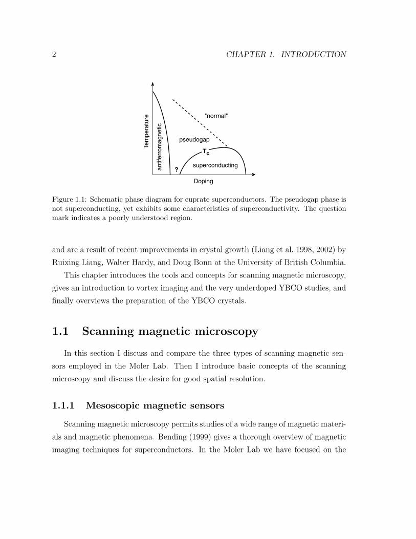
cuprates exhibits numerous phases, which are shown in Figure 1.1. Theories of cuprate
superconductivity make some of their strongest predictions for the very underdoped
region where the superfluid density is low, the sample is deep in the pseudogap in
its “normal” state, and the doping level is close to the antiferromagnetic insulating
phase. For this reason it is important to study very underdoped cuprates to help
illuminate the mechanism of the superconductivity.
Our scanning magnetic microscopy studies of the very underdoped cuprate super-
conductor YBa2Cu3O6+x (YBCO), with x ∼ 6.35, have refuted a promising theory
of spin-charge separation (Wynn et al. 2001; Bonn et al. 2001), given information
about vortex pinning forces (Gardner et al. 2002), enabled measurements of the in-
plane penetration depth, and revealed surprising “partial vortices” in the lowest Tc
samples. High quality very underdoped YBCO crystals were crucial to these studies
1
2 CHAPTER 1. INTRODUCTION
superconductinga
ntife
rro
ma
gn
etic
pseudogap
Doping
Te
mp
era
ture
Tc
?
"normal"
Figure 1.1: Schematic phase diagram for cuprate superconductors. The pseudogap phase isnot superconducting, yet exhibits some characteristics of superconductivity. The questionmark indicates a poorly understood region.
and are a result of recent improvements in crystal growth (Liang et al. 1998, 2002) by
Ruixing Liang, Walter Hardy, and Doug Bonn at the University of British Columbia.
This chapter introduces the tools and concepts for scanning magnetic microscopy,
gives an introduction to vortex imaging and the very underdoped YBCO studies, and
finally overviews the preparation of the YBCO crystals.
1.1 Scanning magnetic microscopy
In this section I discuss and compare the three types of scanning magnetic sen-
sors employed in the Moler Lab. Then I introduce basic concepts of the scanning
microscopy and discuss the desire for good spatial resolution.
1.1.1 Mesoscopic magnetic sensors
Scanning magnetic microscopy permits studies of a wide range of magnetic materi-
als and magnetic phenomena. Bending (1999) gives a thorough overview of magnetic
imaging techniques for superconductors. In the Moler Lab we have focused on the
1.1. SCANNING MAGNETIC MICROSCOPY 3
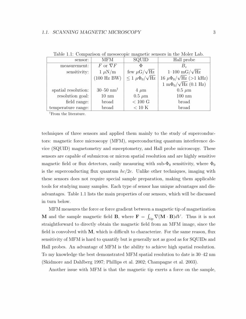
Table 1.1: Comparison of mesoscopic magnetic sensors in the Moler Lab.sensor: MFM SQUID Hall probe
measurement: F or ∇F Φ Bz
sensitivity: 1 µN/m few µG/√
Hz 1–100 mG/√
Hz
(100 Hz BW) ≤ 1 µΦ0/√
Hz 16 µΦ0/√
Hz (>1 kHz)
1 mΦ0/√
Hz (0.1 Hz)spatial resolution: 30–50 nm† 4 µm 0.5 µm
resolution goal: 10 nm 0.5 µm 100 nmfield range: broad < 100 G broad
temperature range: broad < 10 K broad†From the literature.
techniques of three sensors and applied them mainly to the study of superconduc-
tors: magnetic force microscopy (MFM), superconducting quantum interference de-
vice (SQUID) magnetometry and susceptometry, and Hall probe microscopy. These
sensors are capable of submicron or micron spatial resolution and are highly sensitive
magnetic field or flux detectors, easily measuring with sub-Φ0 sensitivity, where Φ0
is the superconducting flux quantum hc/2e. Unlike other techniques, imaging with
these sensors does not require special sample preparation, making them applicable
tools for studying many samples. Each type of sensor has unique advantages and dis-
advantages. Table 1.1 lists the main properties of our sensors, which will be discussed
in turn below.
MFM measures the force or force gradient between a magnetic tip of magnetization
M and the sample magnetic field B, where F =∫
tip∇(M · B)dV . Thus it is not
straightforward to directly obtain the magnetic field from an MFM image, since the
field is convolved with M, which is difficult to characterize. For the same reason, flux
sensitivity of MFM is hard to quantify but is generally not as good as for SQUIDs and
Hall probes. An advantage of MFM is the ability to achieve high spatial resolution.
To my knowledge the best demonstrated MFM spatial resolution to date is 30–42 nm
(Skidmore and Dahlberg 1997; Phillips et al. 2002; Champagne et al. 2003).
Another issue with MFM is that the magnetic tip exerts a force on the sample,
4 CHAPTER 1. INTRODUCTION
potentially disrupting the features of interest. Hug et al. (1994) were the first to ob-
serve individual vortices with an MFM and saw that the tip perturbed the vortices.
While this tip force is generally a disadvantage, it could be used to study vortex pin-
ning forces in superconductors. Eric Straver has built and is using a low temperature
MFM in the Moler Lab. MFM can operate over broad temperature and field ranges.
SQUIDs are currently the most sensitive magnetic flux detectors. Scanning
SQUIDs measure the magnetic flux through a small pick-up loop, Φ =∫loop
B · da,
with sensitivity down to ∼1 µΦ0/√
Hz. Our SQUIDs are specially designed with an
additional loop concentric with the pick-up loop which allows a local field to be applied
to the sample. This allows the SQUID to also operate as a scanning susceptometer
by measuring the response of a sample to a locally applied field (Gardner et al. 2001).
Limitations of SQUIDs are in their spatial resolution, field range, and operating tem-
perature. The linewidth of the superconducting wires is the limiting factor for the
SQUID pick-up loop size, since the wire width cannot be smaller than the penetra-
tion depth of the superconducting material. Our smallest scanning SQUIDs were
designed and fabricated by Martin Huber (CU-Denver) with 4 µm diameter pick-up
loops. The SQUIDs used in this dissertation had 8 µm square pick-up loops and were
made by the commercial foundry HYPRES.1 SQUIDs operate at low fields and low
temperatures (<9 K for Nb).
Scanning SQUIDs have been developed and implemented by a number of groups,
for example Dale van Harlingen at Illinois, John Kirtley at IBM, John Clarke at UC
Berkeley, Fred Wellstood at Maryland, and our group at Stanford. The summary
article by Kirtley (2002) gives an overview of advances in and recent uses of meso-
scopic scanning SQUIDs. The best flux sensitivity reported for scanning SQUIDs
is slightly above 10−6 Φ0/√
Hz for Nb SQUIDs with 4–10 µm pick-up loops (Vu
et al. 1993; Kirtley et al. 1995b; Gardner et al. 2001). High-Tc SQUIDs are also
used in scanning, but their sensitivity is about an order of magnitude worse than
for low-Tc SQUIDs with equivalent spatial resolution (Wellstood et al. 1997). The
smallest SQUIDs reported to date were fabricated by Hasselbach et al. (2000) from
Al and Nb with 1 µm pick-up loops. The sensitivity limit on these probes was not
1http://www.hypres.com/
1.1. SCANNING MAGNETIC MICROSCOPY 5
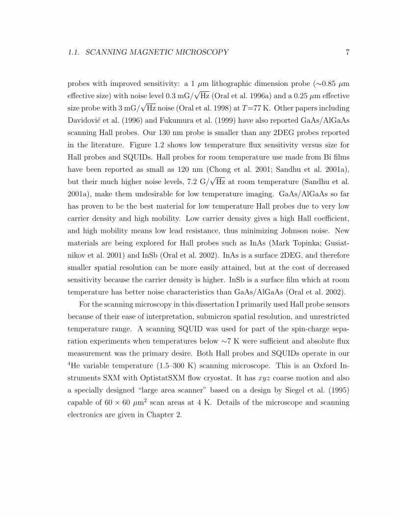
10−1
100
101
102
10−6
10−5
10−4
10−3
10−2
A
B
CD
E
FG
H
I
Sensor Size (µm)
Min
imum
Flu
x S
ensi
tivity
( Φ
0/Hz1/
2 )
Hall ProbesSQUIDs
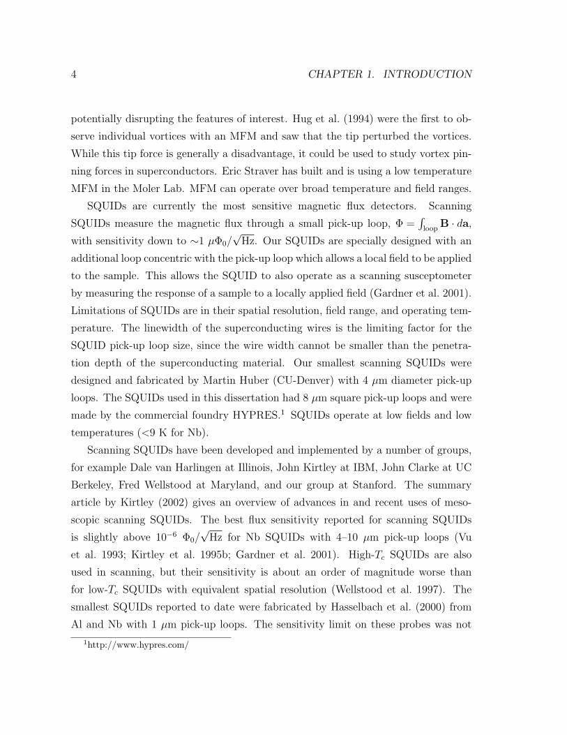
Figure 1.2: Flux sensitivity (white noise floor) versus lithographic sensor size for SQUIDsand Hall probes from the literature (open markers) and the Moler Lab (solid markers). Hallprobes: (A) Chang et al. (1992), (B) Davidovic et al. (1996), (C) Oral et al. (1996a) [77 K],(D) Oral et al. (1998) [77 K], and (E) Grigorenko et al. (2001) [77 K; GaAs/InAs/GaSb].SQUIDs: (F) Vu et al. (1993), (G) Kirtley et al. (1995b), (H) Stawiasz et al. (1995), and(I) Hasselbach et al. (2000) [Al]. Unless otherwise noted: T ≤ 5 K, Hall probes wereGaAs/AlGaAs, and SQUIDs were Nb. For Hall probes (D) and (E), effective size was usedsince lithographic size was not specified.
as good, 3.7× 10⁻⁵ Φ0/√
Hz for Al and higher for Nb, and they also had undesirable
hysteresis. Figure 1.2 (circles) shows flux sensitivity versus pick-up loop size for a
number of SQUIDs.
Hall probes have the advantage of being direct magnetic field sensors, because the
measured Hall voltage is directly proportional to the perpendicular magnetic field
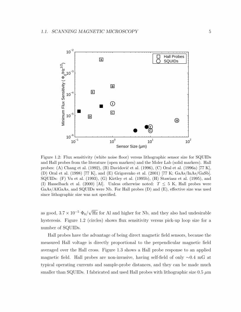
averaged over the Hall cross. Figure 1.3 shows a Hall probe response to an applied
magnetic field. Hall probes are non-invasive, having self-field of only ∼0.4 mG at
typical operating currents and sample-probe distances, and they can be made much
smaller than SQUIDs. I fabricated and used Hall probes with lithographic size 0.5 µm
6 CHAPTER 1. INTRODUCTION
−200 −100 0 100 200−150
−100
−50
0
50
100
150
Bapplied
(Gauss)
Vxy
− V
offs
et (
µV)
−0.5 0 0.5−0.5
0
0.5
Figure 1.3: Hall probe response to applied field for a 0.5 µm probe. The slope gives the Hallcoefficient RH = 0.114 Ω/G. The measurement was made at T = 4.8 K and Ibias = 5.5 µAwith f = 1 kHz using lock-in detection with τ = 0.1 s. Inset: Smaller field sweep givingBnoise ≈ 100 mG.
for scanning, and Clifford Hicks later fabricated probes with lithographic size as small
as 130 nm. These probes were made from GaAs/AlGaAs two-dimensional electron
gas (2DEG) heterostructures (Section 3.3) which have shown themselves to be the
lowest noise materials for low temperature Hall probes. Field sensitivity of our probes
at 4 K ranges from 0.1–20 mG/√
Hz for f ≥ 104 Hz and from 0.005–1 G/√
Hz for
0.1 Hz, for probe sizes of 10 µm down to 130 nm (generally better field sensitivity
is achieved for larger probes). Our best demonstrated flux sensitivity was for the
130 nm probe with 16 µΦ0/√
Hz for >1 kHz and 1 mΦ0/√
Hz for 0.1 Hz. Hall probes,
like MFM, operate over broad field and temperature ranges.
Chang et al. (1992) pioneered high sensitivity submicron SHPM with a Hall probe
fabricated from GaAs/AlGaAs. Their probe had lithographic size 0.5 µm (effective ge-
ometric size ∼0.35 µm due to 2DEG depletion width) and a minimum field noise den-
sity of 0.36 G/√
Hz at T=4 K. Simon Bending’s group later fabricated GaAs/AlGaAs
1.1. SCANNING MAGNETIC MICROSCOPY 7
probes with improved sensitivity: a 1 µm lithographic dimension probe (∼0.85 µm
effective size) with noise level 0.3 mG/√
Hz (Oral et al. 1996a) and a 0.25 µm effective
size probe with 3 mG/√
Hz noise (Oral et al. 1998) at T=77 K. Other papers including
Davidovic et al. (1996) and Fukumura et al. (1999) have also reported GaAs/AlGaAs
scanning Hall probes. Our 130 nm probe is smaller than any 2DEG probes reported
in the literature. Figure 1.2 shows low temperature flux sensitivity versus size for
Hall probes and SQUIDs. Hall probes for room temperature use made from Bi films
have been reported as small as 120 nm (Chong et al. 2001; Sandhu et al. 2001a),
but their much higher noise levels, 7.2 G/√
Hz at room temperature (Sandhu et al.
2001a), make them undesirable for low temperature imaging. GaAs/AlGaAs so far
has proven to be the best material for low temperature Hall probes due to very low
carrier density and high mobility. Low carrier density gives a high Hall coefficient,
and high mobility means low lead resistance, thus minimizing Johnson noise. New
materials are being explored for Hall probes such as InAs (Mark Topinka; Gusiat-
nikov et al. 2001) and InSb (Oral et al. 2002). InAs is a surface 2DEG, and therefore
smaller spatial resolution can be more easily attained, but at the cost of decreased
sensitivity because the carrier density is higher. InSb is a surface film which at room
temperature has better noise characteristics than GaAs/AlGaAs (Oral et al. 2002).
For the scanning microscopy in this dissertation I primarily used Hall probe sensors
because of their ease of interpretation, submicron spatial resolution, and unrestricted
temperature range. A scanning SQUID was used for part of the spin-charge sepa-
ration experiments when temperatures below ∼7 K were sufficient and absolute flux
measurement was the primary desire. Both Hall probes and SQUIDs operate in our4He variable temperature (1.5–300 K) scanning microscope. This is an Oxford In-
struments SXM with OptistatSXM flow cryostat. It has xyz coarse motion and also
a specially designed “large area scanner” based on a design by Siegel et al. (1995)
capable of 60 × 60 µm2 scan areas at 4 K. Details of the microscope and scanning
electronics are given in Chapter 2.
8 CHAPTER 1. INTRODUCTION
10 µm
y
x
z
25 µm 25 µm
B
(a)
(b) (c) (d)
∆B=113 G ∆B=237 G∆B=34 G
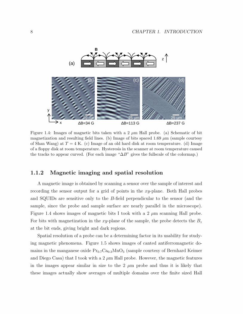
Figure 1.4: Images of magnetic bits taken with a 2 µm Hall probe. (a) Schematic of bitmagnetization and resulting field lines. (b) Image of bits spaced 1.69 µm (sample courtesyof Shan Wang) at T = 4 K. (c) Image of an old hard disk at room temperature. (d) Imageof a floppy disk at room temperature. Hysteresis in the scanner at room temperature causedthe tracks to appear curved. (For each image “∆B” gives the fullscale of the colormap.)
1.1.2 Magnetic imaging and spatial resolution
A magnetic image is obtained by scanning a sensor over the sample of interest and
recording the sensor output for a grid of points in the xy-plane. Both Hall probes
and SQUIDs are sensitive only to the B-field perpendicular to the sensor (and the
sample, since the probe and sample surface are nearly parallel in the microscope).
Figure 1.4 shows images of magnetic bits I took with a 2 µm scanning Hall probe.
For bits with magnetization in the xy-plane of the sample, the probe detects the Bz
at the bit ends, giving bright and dark regions.
Spatial resolution of a probe can be a determining factor in its usability for study-
ing magnetic phenomena. Figure 1.5 shows images of canted antiferromagnetic do-
mains in the manganese oxide Pr0.7Ca0.3MnO3 (sample courtesy of Bernhard Keimer
and Diego Casa) that I took with a 2 µm Hall probe. However, the magnetic features
in the images appear similar in size to the 2 µm probe and thus it is likely that
these images actually show averages of multiple domains over the finite sized Hall
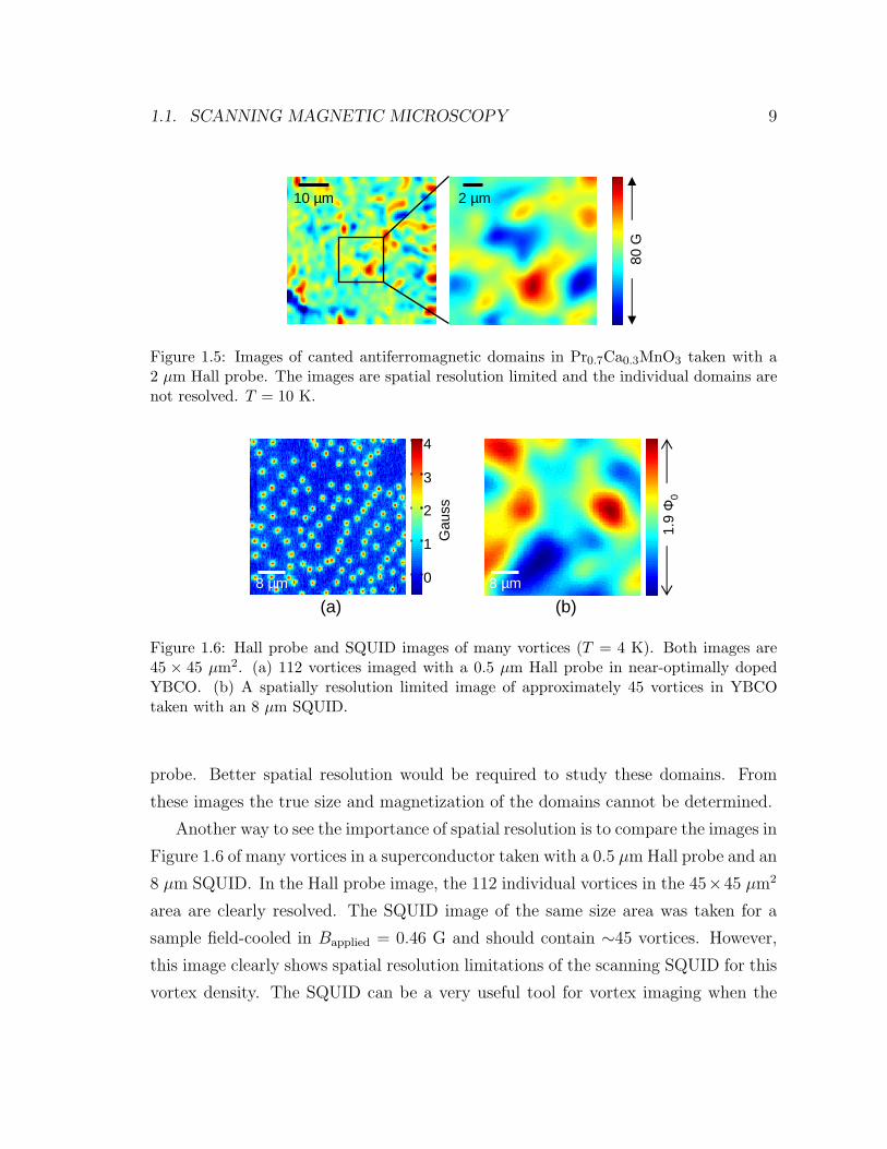
1.1. SCANNING MAGNETIC MICROSCOPY 9
80 G
2 µm10 µm
Figure 1.5: Images of canted antiferromagnetic domains in Pr0.7Ca0.3MnO3 taken with a2 µm Hall probe. The images are spatial resolution limited and the individual domains arenot resolved. T = 10 K.
0
1
2
3
4G
auss
1.9
Φ0
(a) (b)8 µm 8 µm
Figure 1.6: Hall probe and SQUID images of many vortices (T = 4 K). Both images are45 × 45 µm2. (a) 112 vortices imaged with a 0.5 µm Hall probe in near-optimally dopedYBCO. (b) A spatially resolution limited image of approximately 45 vortices in YBCOtaken with an 8 µm SQUID.
probe. Better spatial resolution would be required to study these domains. From
these images the true size and magnetization of the domains cannot be determined.
Another way to see the importance of spatial resolution is to compare the images in
Figure 1.6 of many vortices in a superconductor taken with a 0.5 µm Hall probe and an
8 µm SQUID. In the Hall probe image, the 112 individual vortices in the 45×45 µm2
area are clearly resolved. The SQUID image of the same size area was taken for a
sample field-cooled in Bapplied = 0.46 G and should contain ∼45 vortices. However,
this image clearly shows spatial resolution limitations of the scanning SQUID for this
vortex density. The SQUID can be a very useful tool for vortex imaging when the
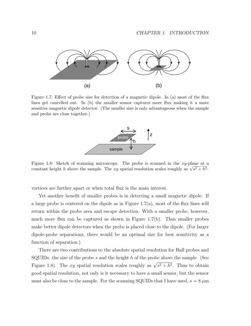
10 CHAPTER 1. INTRODUCTION
(a) (b)
Figure 1.7: Effect of probe size for detection of a magnetic dipole. In (a) most of the fluxlines get cancelled out. In (b) the smaller sensor captures more flux making it a moresensitive magnetic dipole detector. (The smaller size is only advantageous when the sampleand probe are close together.)
zh
s
probe
sample
Figure 1.8: Sketch of scanning microscopy. The probe is scanned in the xy-plane at aconstant height h above the sample. The xy spatial resolution scales roughly as
√s2 + h2.
vortices are further apart or when total flux is the main interest.
Yet another benefit of smaller probes is in detecting a small magnetic dipole. If
a large probe is centered on the dipole as in Figure 1.7(a), most of the flux lines will
return within the probe area and escape detection. With a smaller probe, however,
much more flux can be captured as shown in Figure 1.7(b). Thus smaller probes
make better dipole detectors when the probe is placed close to the dipole. (For larger
dipole-probe separations, there would be an optimal size for best sensitivity as a
function of separation.)
There are two contributions to the absolute spatial resolution for Hall probes and
SQUIDs: the size of the probe s and the height h of the probe above the sample. (See
Figure 1.8). The xy spatial resolution scales roughly as√
s2 + h2. Thus to obtain
good spatial resolution, not only is it necessary to have a small sensor, but the sensor
must also be close to the sample. For the scanning SQUIDs that I have used, s = 8 µm
1.1. SCANNING MAGNETIC MICROSCOPY 11
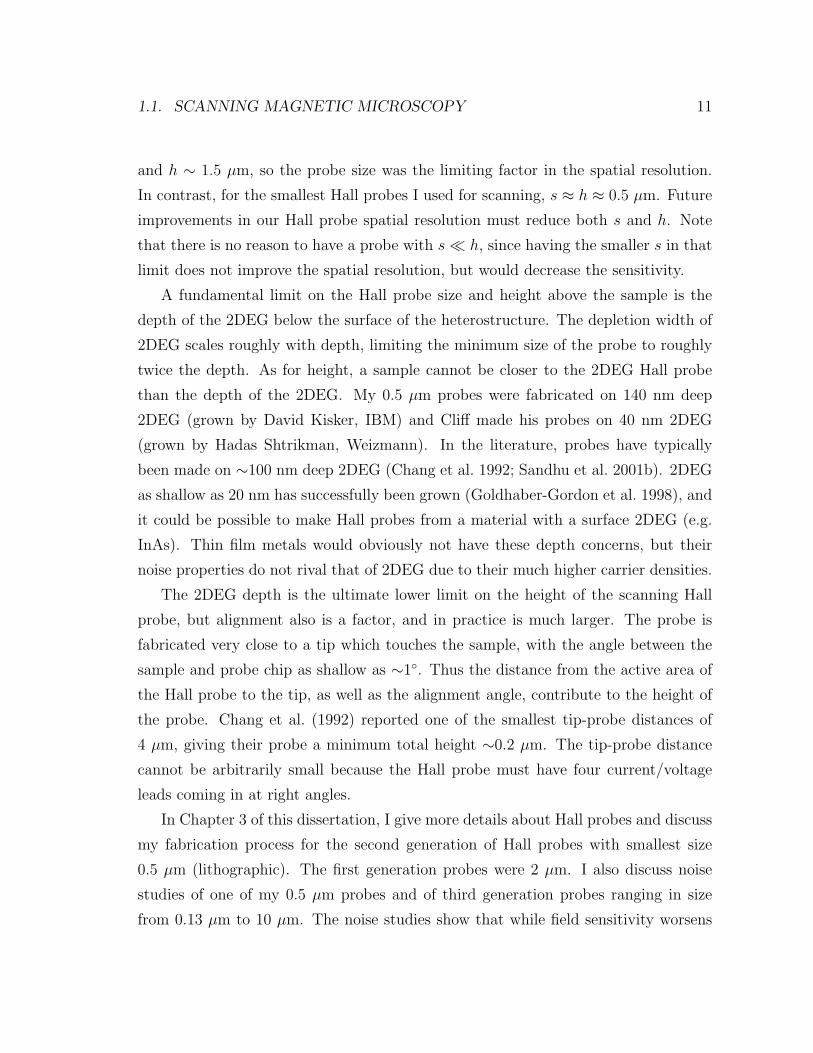
and h ∼ 1.5 µm, so the probe size was the limiting factor in the spatial resolution.
In contrast, for the smallest Hall probes I used for scanning, s ≈ h ≈ 0.5 µm. Future
improvements in our Hall probe spatial resolution must reduce both s and h. Note
that there is no reason to have a probe with s ¿ h, since having the smaller s in that
limit does not improve the spatial resolution, but would decrease the sensitivity.
A fundamental limit on the Hall probe size and height above the sample is the
depth of the 2DEG below the surface of the heterostructure. The depletion width of
2DEG scales roughly with depth, limiting the minimum size of the probe to roughly
twice the depth. As for height, a sample cannot be closer to the 2DEG Hall probe
than the depth of the 2DEG. My 0.5 µm probes were fabricated on 140 nm deep
2DEG (grown by David Kisker, IBM) and Cliff made his probes on 40 nm 2DEG
(grown by Hadas Shtrikman, Weizmann). In the literature, probes have typically
been made on ∼100 nm deep 2DEG (Chang et al. 1992; Sandhu et al. 2001b). 2DEG
as shallow as 20 nm has successfully been grown (Goldhaber-Gordon et al. 1998), and
it could be possible to make Hall probes from a material with a surface 2DEG (e.g.
InAs). Thin film metals would obviously not have these depth concerns, but their
noise properties do not rival that of 2DEG due to their much higher carrier densities.
The 2DEG depth is the ultimate lower limit on the height of the scanning Hall
probe, but alignment also is a factor, and in practice is much larger. The probe is
fabricated very close to a tip which touches the sample, with the angle between the
sample and probe chip as shallow as ∼1. Thus the distance from the active area of
the Hall probe to the tip, as well as the alignment angle, contribute to the height of
the probe. Chang et al. (1992) reported one of the smallest tip-probe distances of
4 µm, giving their probe a minimum total height ∼0.2 µm. The tip-probe distance
cannot be arbitrarily small because the Hall probe must have four current/voltage
leads coming in at right angles.
In Chapter 3 of this dissertation, I give more details about Hall probes and discuss
my fabrication process for the second generation of Hall probes with smallest size
0.5 µm (lithographic). The first generation probes were 2 µm. I also discuss noise
studies of one of my 0.5 µm probes and of third generation probes ranging in size
from 0.13 µm to 10 µm. The noise studies show that while field sensitivity worsens
12 CHAPTER 1. INTRODUCTION
as Hall probe size is decreased, flux sensitivity improves. This holds promise that
sub-100 nm probes can be fabricated without compromising flux sensitivity.
1.2 Vortex imaging
In this section I will give a brief review of vortices in superconductors, motivation
for why we should image them, and finally an introduction to the vortex imaging
experiments on very underdoped YBa2Cu3O6+x described in Chapters 4–6.
1.2.1 The basics
My main use of the scanning Hall probe (and SQUID) microscope has been to
image magnetic vortices in superconductors, primarily in very underdoped YBCO.
Hallmarks of superconductivity are zero DC resistance and the expulsion of magnetic
field (the Meissner Effect). In type II superconductors, instead of full field expulsion,
for a range of fields it is energetically favorable for the magnetic flux to enter the
superconductor in bundles, which can also be thought of as vortices of supercurrent
around a normal core. This occurs in type II superconductors because λ is larger
than ξ, which makes the energy of a superconducting-normal interface negative, and
so the superconductor lowers its energy by allowing normal regions (the flux bundles).
The penetration depth, λ, is the length scale of magnetic field penetration into a
superconductor, while the coherence length, ξ, is the length scale over which the
superconducting order parameter can change. The phase of the superconducting
order parameter must be single valued and this leads to fluxoid quantization: Φ +
(m∗c/e∗)∮
vs · ds = nΦ0 (see Tinkham 1996, p. 127), where Φ0 = hc/e∗ and e∗ = 2e
for Cooper pairs. For an isolated vortex in a sample large compared to the penetration
depth, there is a line integral where vs = 0, so the vortex flux Φ is quantized. The
superfluid energy of a vortex scales as flux squared, and as mentioned above the
interface energy of the normal core is negative, so to minimize the free energy the
flux is split up into as many vortices as possible each carrying the minimum allowed
flux of Φ0.
1.2. VORTEX IMAGING 13
The penetration depth and coherence length are key length scales in a supercon-
ductor. In terms of vortices, ξ is the size of the vortex core and λ is the extent of
the vortex magnetic field. The coherence length is small in the YBCO and cannot be
measured with our scanning magnetic probes. On the other hand, the penetration
depth affects the field profile of the vortex which is imaged by the scanning probe.
(The coherence length also affects the field profile by cutting off the singularity at
the vortex center.) λ is related to the superfluid density, ns/m∗, by the relation
4πλ2/c2 = m∗/nse2. The penetration depth, if measured experimentally, can give
direct information about the superconducting state. For high temperature supercon-
ductors whose mechanism has yet to be understood, measurements of the superfluid
density are of great theoretical importance.
The field of a vortex inside a superconductor is spread out on the length scale λ.
Near the surface of the superconductor the flux spreads out further starting at a depth
of approximately λ. The exact field profile inside and outside the superconductor can
be solved from London theory. Above the superconductor at distances large compared
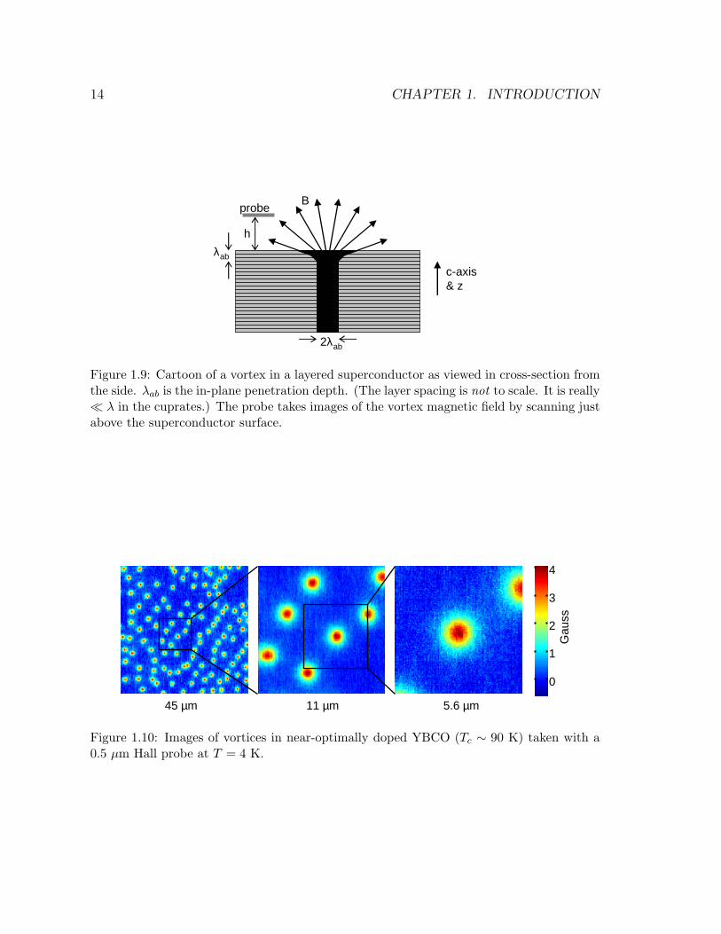
to λ, the vortex profile resembles that of a magnetic monopole located a distance λ
beneath the surface (Pearl 1966). The scanning magnetic microscope images the
vortex field profile just above the superconductor surface. Cuprates are anisotropic
superconductors and the relevant penetration depth for vortices perpendicular to the
planes (c-axis vortices) is the in-plane penetration depth λab (Chang et al. 1992; Kogan
et al. 1993). See Figure 1.9 for a cartoon of a vortex and Figure 1.10 for Hall probe
images of vortices in a near-optimally doped YBCO crystal. Other experiments have
measured λab ∼ 0.16 µm for T → 0 in optimally doped YBCO (Basov et al. 1995),
so these images are resolution-limited.
Scanning Hall probe microscopy of individual vortices and the determination of λ
from the images was first demonstrated by Chang et al. (1992) for a superconducting
thin film. Oral et al. (1996b) and Davidovic et al. (1996) also achieved scanning Hall
probe microscopy of single vortices several years later.
14 CHAPTER 1. INTRODUCTION
2λab
λab
probe
h
B
c-axis& z
Figure 1.9: Cartoon of a vortex in a layered superconductor as viewed in cross-section fromthe side. λab is the in-plane penetration depth. (The layer spacing is not to scale. It is really¿ λ in the cuprates.) The probe takes images of the vortex magnetic field by scanning justabove the superconductor surface.
0
1
2
3
4G
auss
45 µm 11 µm 5.6 µm
Figure 1.10: Images of vortices in near-optimally doped YBCO (Tc ∼ 90 K) taken with a0.5 µm Hall probe at T = 4 K.
1.2. VORTEX IMAGING 15
1.2.2 Experiments in very underdoped YBCO
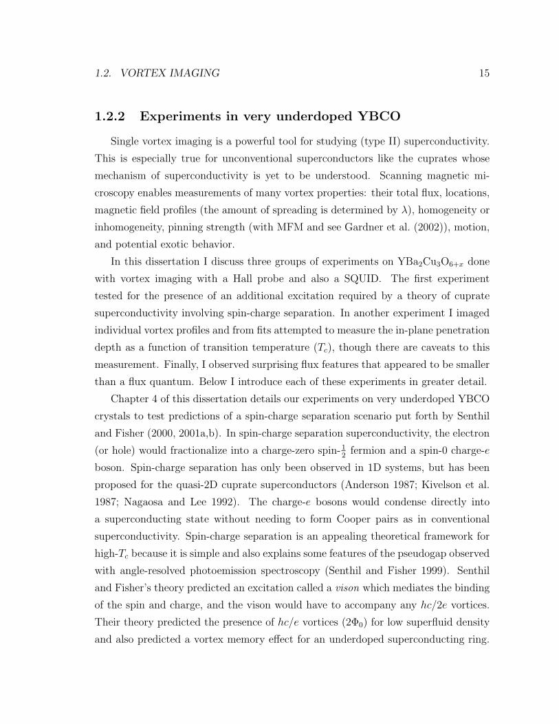
Single vortex imaging is a powerful tool for studying (type II) superconductivity.
This is especially true for unconventional superconductors like the cuprates whose
mechanism of superconductivity is yet to be understood. Scanning magnetic mi-
croscopy enables measurements of many vortex properties: their total flux, locations,
magnetic field profiles (the amount of spreading is determined by λ), homogeneity or
inhomogeneity, pinning strength (with MFM and see Gardner et al. (2002)), motion,
and potential exotic behavior.
In this dissertation I discuss three groups of experiments on YBa2Cu3O6+x done
with vortex imaging with a Hall probe and also a SQUID. The first experiment
tested for the presence of an additional excitation required by a theory of cuprate
superconductivity involving spin-charge separation. In another experiment I imaged
individual vortex profiles and from fits attempted to measure the in-plane penetration
depth as a function of transition temperature (Tc), though there are caveats to this
measurement. Finally, I observed surprising flux features that appeared to be smaller
than a flux quantum. Below I introduce each of these experiments in greater detail.
Chapter 4 of this dissertation details our experiments on very underdoped YBCO
crystals to test predictions of a spin-charge separation scenario put forth by Senthil
and Fisher (2000, 2001a,b). In spin-charge separation superconductivity, the electron
(or hole) would fractionalize into a charge-zero spin-12
fermion and a spin-0 charge-e
boson. Spin-charge separation has only been observed in 1D systems, but has been
proposed for the quasi-2D cuprate superconductors (Anderson 1987; Kivelson et al.
1987; Nagaosa and Lee 1992). The charge-e bosons would condense directly into
a superconducting state without needing to form Cooper pairs as in conventional
superconductivity. Spin-charge separation is an appealing theoretical framework for
high-Tc because it is simple and also explains some features of the pseudogap observed
with angle-resolved photoemission spectroscopy (Senthil and Fisher 1999). Senthil
and Fisher’s theory predicted an excitation called a vison which mediates the binding
of the spin and charge, and the vison would have to accompany any hc/2e vortices.
Their theory predicted the presence of hc/e vortices (2Φ0) for low superfluid density
and also predicted a vortex memory effect for an underdoped superconducting ring.
16 CHAPTER 1. INTRODUCTION
Using scanning SQUIDs and Hall probes, we searched for these double vortices and the
memory effect in very underdoped YBCO, but did not find either. These experiments
(Wynn et al. 2001; Bonn et al. 2001) set a strict upper bound on the energy of the
vison incompatible with the theory, thus ruling out as the mechanism of cuprate
superconductivity all scenarios of spin-charge separation which require visons.
My next experiment was motivated by vortex images from the spin-charge sepa-
ration experiments which suggested that the extent of the vortex field was at least
1 µm in very underdoped YBCO. If the vortices are described by London theory,
the in-plane penetration depth λab is the vortex extent. This inferred λab ≈ 1 µm
would be larger than predicted by the Uemura relation Tc ∝ ns(0)/m∗ for underdoped
cuprates. Uemura et al. (1989, 1991) performed muon spin resonance measurements
of the penetration depth on many high-Tc samples and other unconventional su-
perconductors. They found a universal linear relationship between the transition
temperature and the zero-temperature superfluid density for the underdoped sam-
ples. Emery and Kivelson (1995a) explained this linear behavior as thermal phase
fluctuations destroying the superconductivity in underdoped samples. For overdoped
samples however, pair breaking dominates (as in BCS theory) and Tc is suppressed
much below the phase-ordering temperature. This linear relation has been widely
accepted as a phenomenological rule, but it has not been tested in extremely un-
derdoped cuprates (with Tc . 0.1 Tc,max). Due to the theoretical importance of the
Uemura relation, it is desirable to test very underdoped samples. Using a submicron
scanning Hall probe I imaged many vortices in YBa2Cu3O6+x with Tc ranging from
5–15 K, then I fit these images to theoretical vortex field profiles in an attempt to
measure λab. This work is described in Chapter 5. However, as discussed in Chapter
5, pinning of the 2D pancake vortices which compose the vortex could broaden the
apparent spreading of the vortex field, so strictly my results should only be inter-
preted as an upper bound on λab. If pinning is not an issue, the results give larger
penetration depths (smaller superfluid density) at the lowest Tc’s than predicted by
the Uemura relation. If this is the case, theory would need to be modified.
Lastly, some images from the most underdoped YBCO samples revealed distinct
flux that appeared to be smaller than Φ0 vortices. These “partial vortices” typically
1.3. VERY UNDERDOPED YBa2Cu3O6+x CRYSTALS 17
appeared in groups and were more mobile than full vortices. I studied these partial
vortices and determined that a likely explanation is partial lateral displacements of
a full vortex. This can only occur in layered superconductors with large anisotropy
where the Josephson coupling between the layers is negligible. In such cases a 3D c-
axis vortex can be thought of as a stack of 2D pancake vortices, one in each layer (Clem
1991). Magnetic interactions and any Josephson coupling favor vertical alignment of
the pancakes, but with a sufficient pinning landscape a straight stack could have a
“split” or “kink” in which a section of the stack is displaced laterally (Benkraouda
and Clem 1996; Grigorenko et al. 2002). From above, the field from the partial stacks
resembles isolated sub-Φ0 flux bundles (i.e. partial vortices). My data show split
displacements as large as tens-of-microns. My observations of these partial vortices
and the model of a split pancake vortex stack are discussed in detail in Chapter 6.
This work reveals new vortex behavior which is dominant in the lowest doped YBCO,
showing that the material is indeed very anisotropic. The split vortex behavior would
be undesirable in technological applications because vortices would be less susceptible
to pinning, which would suppress the critical current.
1.3 Very underdoped YBa2Cu3O6+x crystals
The vortex imaging experiments described in Chapters 4–6 of this dissertation
would not have been possible without the high-purity very underdoped YBa2Cu3O6+x
single crystals grown by Ruixing Liang in the group of Doug Bonn and Walter Hardy
at the University of British Columbia.
Three of the most studied cuprates are Bi2Sr2CaCu2O8+x (BSCCO),
La2−xSrxCuO4 (LSCO),2 and YBa2Cu3O6+x (YBCO). The value of x in each case
tunes the hole doping in the two-dimensional CuO2 planes where superconductivity
occurs. Doping increases with x. Optimal doping (that which gives the maximum
Tc) occurs at x ≈ 0.16 and Tc ≈ 92 K for BSCCO, x = 0.16 and Tc = 39 K for
2A similar compound to La2−xSrxCuO4 is La2−xBaxCuO4 which was the first high temperaturesuperconductor discovered (Bednorz and Muller 1986). The Sr and Ba play similar roles, thoughthe Sr compound gives somewhat higher Tc.
18 CHAPTER 1. INTRODUCTION
cb
a
Barium
Copper
Oxygen
Oxygen or vacancy
Yttrium
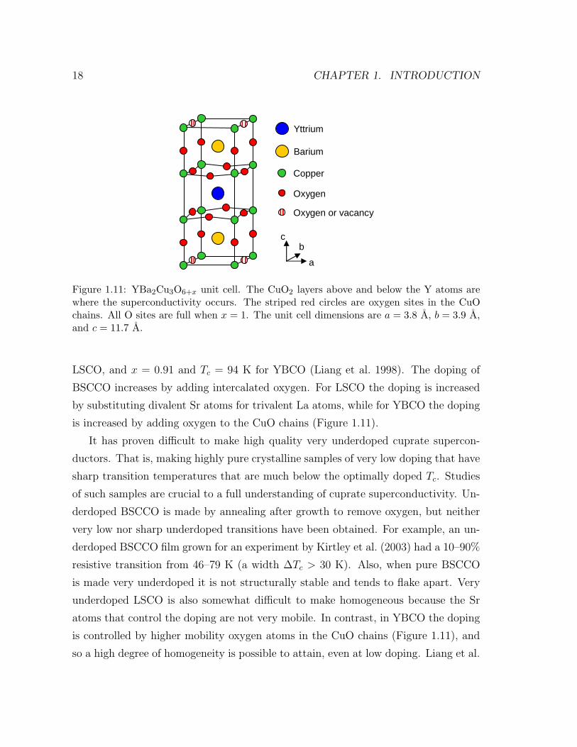
Figure 1.11: YBa2Cu3O6+x unit cell. The CuO2 layers above and below the Y atoms arewhere the superconductivity occurs. The striped red circles are oxygen sites in the CuOchains. All O sites are full when x = 1. The unit cell dimensions are a = 3.8 A, b = 3.9 A,and c = 11.7 A.
LSCO, and x = 0.91 and Tc = 94 K for YBCO (Liang et al. 1998). The doping of
BSCCO increases by adding intercalated oxygen. For LSCO the doping is increased
by substituting divalent Sr atoms for trivalent La atoms, while for YBCO the doping
is increased by adding oxygen to the CuO chains (Figure 1.11).
It has proven difficult to make high quality very underdoped cuprate supercon-
ductors. That is, making highly pure crystalline samples of very low doping that have
sharp transition temperatures that are much below the optimally doped Tc. Studies
of such samples are crucial to a full understanding of cuprate superconductivity. Un-
derdoped BSCCO is made by annealing after growth to remove oxygen, but neither
very low nor sharp underdoped transitions have been obtained. For example, an un-
derdoped BSCCO film grown for an experiment by Kirtley et al. (2003) had a 10–90%
resistive transition from 46–79 K (a width ∆Tc > 30 K). Also, when pure BSCCO
is made very underdoped it is not structurally stable and tends to flake apart. Very
underdoped LSCO is also somewhat difficult to make homogeneous because the Sr
atoms that control the doping are not very mobile. In contrast, in YBCO the doping
is controlled by higher mobility oxygen atoms in the CuO chains (Figure 1.11), and
so a high degree of homogeneity is possible to attain, even at low doping. Liang et al.
1.3. VERY UNDERDOPED YBa2Cu3O6+x CRYSTALS 19
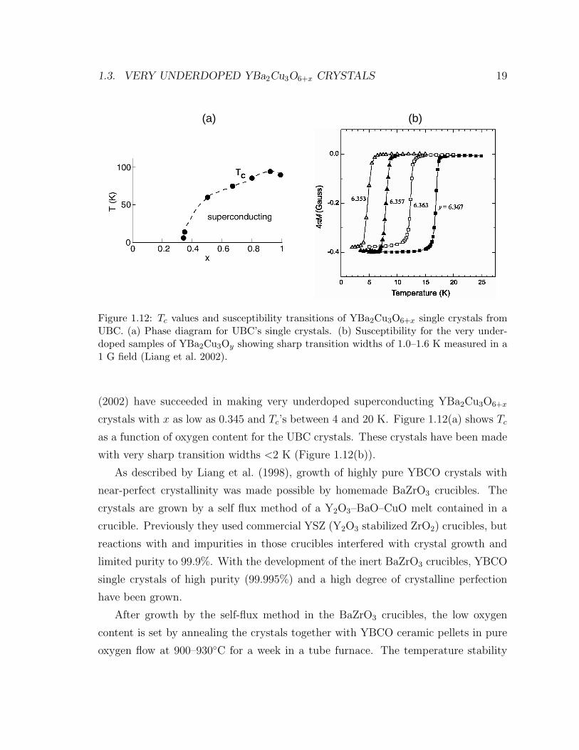
(b)(a)
Figure 1.12: Tc values and susceptibility transitions of YBa2Cu3O6+x single crystals fromUBC. (a) Phase diagram for UBC’s single crystals. (b) Susceptibility for the very under-doped samples of YBa2Cu3Oy showing sharp transition widths of 1.0–1.6 K measured in a1 G field (Liang et al. 2002).
(2002) have succeeded in making very underdoped superconducting YBa2Cu3O6+x
crystals with x as low as 0.345 and Tc’s between 4 and 20 K. Figure 1.12(a) shows Tc
as a function of oxygen content for the UBC crystals. These crystals have been made
with very sharp transition widths <2 K (Figure 1.12(b)).
As described by Liang et al. (1998), growth of highly pure YBCO crystals with
near-perfect crystallinity was made possible by homemade BaZrO3 crucibles. The
crystals are grown by a self flux method of a Y2O3–BaO–CuO melt contained in a
crucible. Previously they used commercial YSZ (Y2O3 stabilized ZrO2) crucibles, but
reactions with and impurities in those crucibles interfered with crystal growth and
limited purity to 99.9%. With the development of the inert BaZrO3 crucibles, YBCO
single crystals of high purity (99.995%) and a high degree of crystalline perfection
have been grown.
After growth by the self-flux method in the BaZrO3 crucibles, the low oxygen
content is set by annealing the crystals together with YBCO ceramic pellets in pure
oxygen flow at 900–930C for a week in a tube furnace. The temperature stability
20 CHAPTER 1. INTRODUCTION
is 0.5C and the temperature setting tunes the exact oxygen content between 6.340
and 6.370. After this anneal, oxygen inhomogeneities are removed during a 1–2 week
570C anneal of the crystals while sealed in a small tube with YBCO ceramic of the
same oxygen content. Afterwards the tube is quenched in ice water. (Liang et al.
2002). The crystals are initially twinned and can be several millimeters in the ab-plane
with typical thickness 10–100 µm in the c-axis direction.
Initially after quenching, the crystals are not superconducting, but annealing at
room temperature allows the chain oxygen atoms to order, increasing the in-plane
doping and the Tc until saturation is reached at Tc = 4–20 K depending on the
oxygen content. During this low temperature anneal, the chain oxygen atoms form
chain fragments in the Ortho-II phase whose increasing lengths provide the carrier
doping in the CuO2 planes. The Ortho-II phase has alternating filled and empty
chains and is stable for oxygen content 6.30–6.60. X-ray diffraction studies verified
that these very underdoped crystals had only Ortho-II ordering and the ordering
correlation lengths were measured to be 1.14(5), 3.6(3), and 1.05(7) nm along the a,
b, and c axes respectively in YBa2Cu3O6.362 crystals. (Liang et al. 2002).
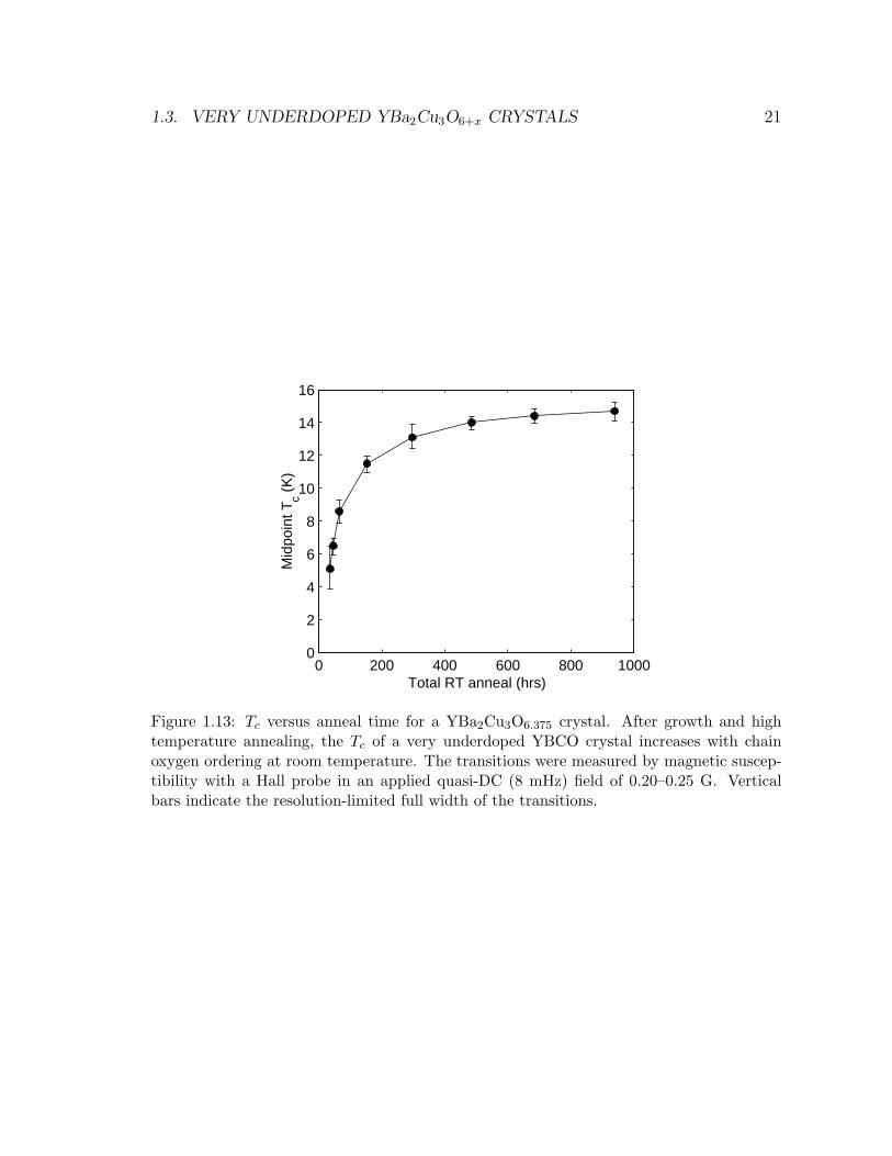
The CuO2 plane doping and thus Tc dependence on room temperature annealing
makes it possible to study a single crystal at many Tc values. For the experiments in
Chapters 5 & 6, I studied one such crystal of YBa2Cu3O6.375 for eight Tc values from 5
to 15 K. Figure 1.13 shows the dependence of Tc on anneal time. The superconducting
transitions were measured with the Hall probe in situ in the scanning microscope. The
vertical error bars indicate the measured full width of the superconducting transition,
limited by the resolution of the measurement technique to ∼10% of the susceptibility.
The transition width is nearly 3 K for the lowest Tc ≈ 5 K, but is sharper than 1.5 K
for all the subsequent Tc’s. A narrow transition width suggests high homogeneity, and
the vortex imaging discussed in Chapter 5 gives further information on the degree of
local homogeneity.
1.3. VERY UNDERDOPED YBa2Cu3O6+x CRYSTALS 21
0 200 400 600 800 10000
2
4
6
8
10
12
14
16
Total RT anneal (hrs)
Mid
poin
t Tc (
K)
Figure 1.13: Tc versus anneal time for a YBa2Cu3O6.375 crystal. After growth and hightemperature annealing, the Tc of a very underdoped YBCO crystal increases with chainoxygen ordering at room temperature. The transitions were measured by magnetic suscep-tibility with a Hall probe in an applied quasi-DC (8 mHz) field of 0.20–0.25 G. Verticalbars indicate the resolution-limited full width of the transitions.
22 CHAPTER 1. INTRODUCTION
Chapter 2
The scanning probe microscope
All the scanning microscopy discussed in this dissertation was done in an Oxford
Instruments SXM scanning probe microscope,1 with extra improvements for scanning
Hall probe and scanning SQUID microscopy. This chapter introduces the cryostat and
the microscope head, followed by the specially designed large area scanner and char-
acterizations thereof. Finally, the probe and sample set-up and scanning electronics
are discussed.
2.1 Variable-temperature flow cryostat
The scanning microscope is housed in a small variable temperature 4He flow cryo-
stat, the Oxford Instruments OptistatSXM, shown in Figure 2.1. The cryostat con-
sists of two concentric vacuum insulated chambers. The microscope head is at the
end of a rod which is inserted in the inner chamber, while the outer chamber holds up
to 4 L of liquid helium. The sample space is connected to the He bath by a capillary
tube at the base of the outer chamber and the opening is controlled by a needle valve.
Sample cooling is achieved by pumping through a port connected to the sample space
and drawing cold He gas from the liquid bath through the needle valve and past the
sample.
Temperature control is achieved with the needle valve and a resistive heater at
1Oxford has since sold their scanning probe microscope division to Omicron NanoTechnology.
23
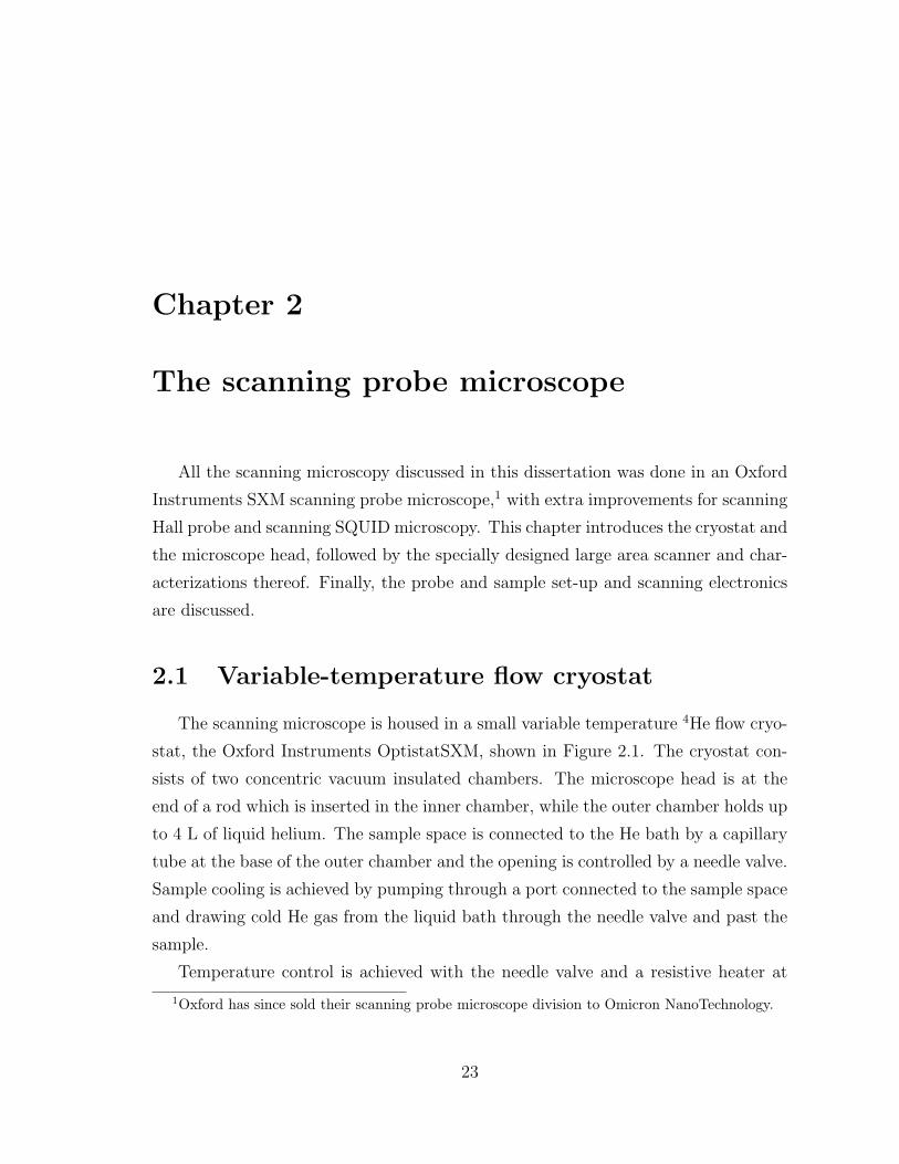
24 CHAPTER 2. THE SCANNING PROBE MICROSCOPE
window to sample space
top of rod
pump line to sample space
bungee cordsuspension
Figure 2.1: The SXM variable temperature 4He flow cryostat.
the base of the sample chamber. The heater is controlled by an Oxford Instruments
ITC-503 temperature controller. The ITC reads temperature from two thermometers:
a RhFe resistor located at the bottom of the sample chamber, and a Cernox resistor
located on the microscope head approximately 1.5 cm to the side of the sample. The
ITC feeds back on the RhFe thermometer by adjusting the heater output to maintain
a set temperature. The needle valve is not controlled by the ITC and must be set
manually to achieve sufficient He flow.
There are two pumps that can be used to cool the sample space. One is a small oil-
free diaphragm pump which I typically used in cooling from room temperature down
to near the desired operating temperature. The second pump is a larger Leybold
SOGEVAC rotary vane pump which can sustain a high pressure flow and enables
cooling to a base temperature of 1.7 K. Temperature stability is more easily achieved
with the larger pump, so I pumped with the SOGEVAC when taking data even when
not near base temperature. The SOGEVAC is housed in an adjacent pump room and
is connected to the cryostat through flexible hoses in a T design to minimize forces and
vibrations on the cryostat. (I used the diaphragm pump for cooling mainly because
it ran quieter.)
2.1. VARIABLE-TEMPERATURE FLOW CRYOSTAT 25
The cryostat can either be mounted on an optical table or suspended. Suspend-
ing it from an aluminum frame with bungee cords was sufficient to get the needed
vibration isolation for Hall probe or SQUID imaging. The suspension scheme also
allows easy insertion into or removal from triple layer mu-metal magnetic shielding.
The residual magnetic field inside the shielding is at most a few tens of mG, as
determined by observations of vortex density in superconducting samples cooled in
zero applied field. This residual field may be due to something magnetic inside the
shielding.
The sample chamber extends 7˝ below the base of the liquid helium chamber and
has 5 ports for optical access to the sample space. There are two windows of Spectrosil
B quartz for side views 180 apart. The other 3 ports (two side ports at 90 from the
windows and one on the bottom) have opaque blanks. The optical access has mainly
been a convenience rather than a necessity for my measurements. When the cryostat
was not inside the magnetic shielding, I could adjust the sample-probe separation
by sight during cooling. Troubleshooting is also easier with optical access in cases
where the sample-probe alignment is off or if a bump on the sample is interfering with
scanning. The windows also enable visual estimates of the angle between the probe
chip and the sample, which is one contribution to the sample-probe height. However,
for reasons that are unclear, this has not always given accurate height measurements.
Another advantage of the windows is the ability to expose the Hall probe to light
in situ. The Hall probe becomes noisier if the probe is electrically shocked or pressed
too far into the sample, but fully recovers with thermal cycling. Exposing the probe
to optical photons sometimes seemed to improve the noise, presumably by photo-
inducing the release of trapped carriers. During data taking with the Hall probe,
the windows were typically covered. A disadvantage of the windows is that they
slowly leak from the room into the outer vacuum chamber (OVC) which insulates the
He bath. Cleaning the windows and regreasing the O-rings did not stop the leaks.
Therefore it has been important to pump out the OVC with a turbo pump for a
day before each cooldown. This especially affected the hold time of liquid nitrogen
during precooling. Poor vacuum in the OVC had less effect on the He bath hold time,
presumably because of cryopumping.
26 CHAPTER 2. THE SCANNING PROBE MICROSCOPE
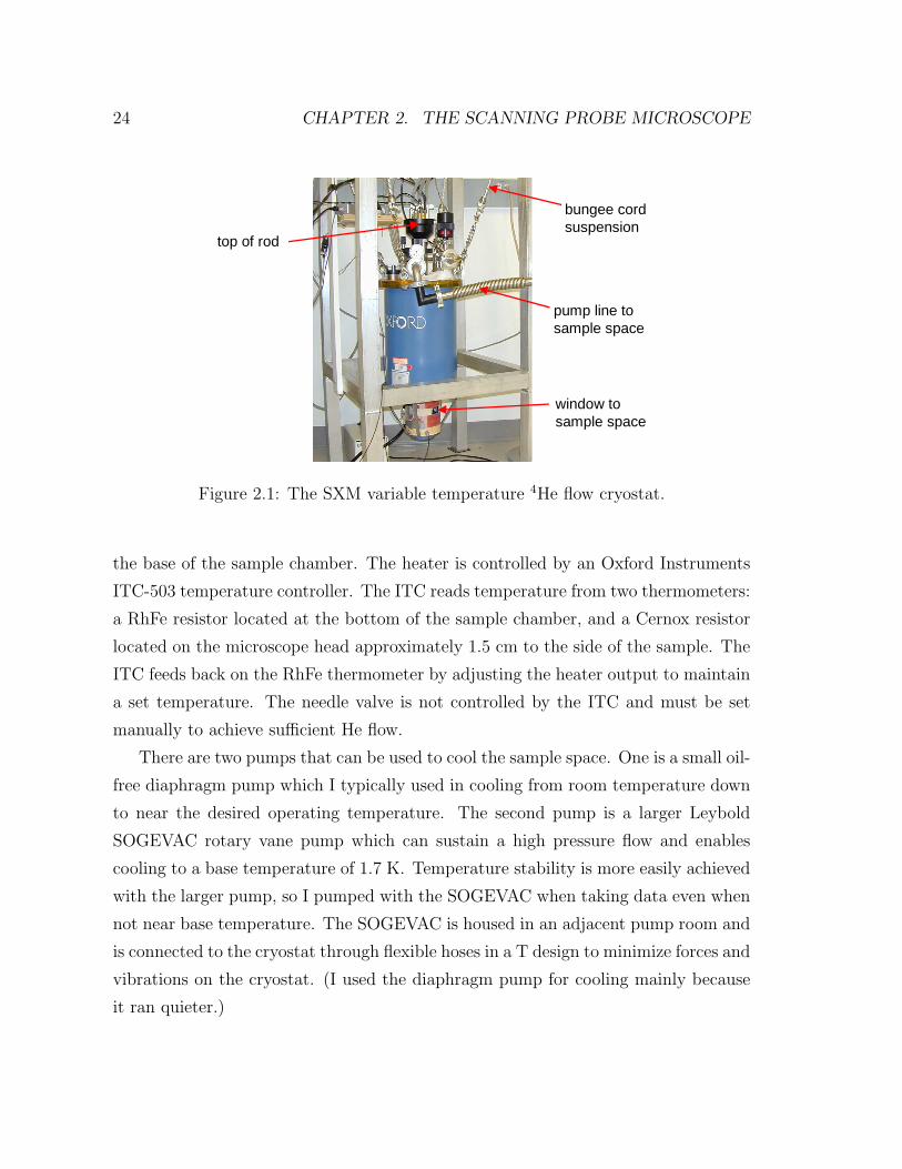
Figure 2.2: Home-wound electromagnets mounted outside the SXM cryostat provide 62 G/Avertically and 4.7 G/A horizontally.
The cryostat is not equipped with a built-in magnet. For my vortex studies only
fields of at most a few Gauss were needed. I wound two electromagnets of copper
wire and mounted them outside the cryostat centered on the sample. See Figure 2.2.
The first provides 62 G/A along the z-axis (vertical and perpendicular to the sample
and probe). It has resistance 122 Ω and inductance <0.2 H. Just recently I added
another electromagnet to provide a small horizontal field for the partial vortex studies
described in Chapter 6. This magnet consists of two 6 cm diameter coils mounted
90 to the windows which together provide 4.7 G/A and have total resistance 25 Ω.
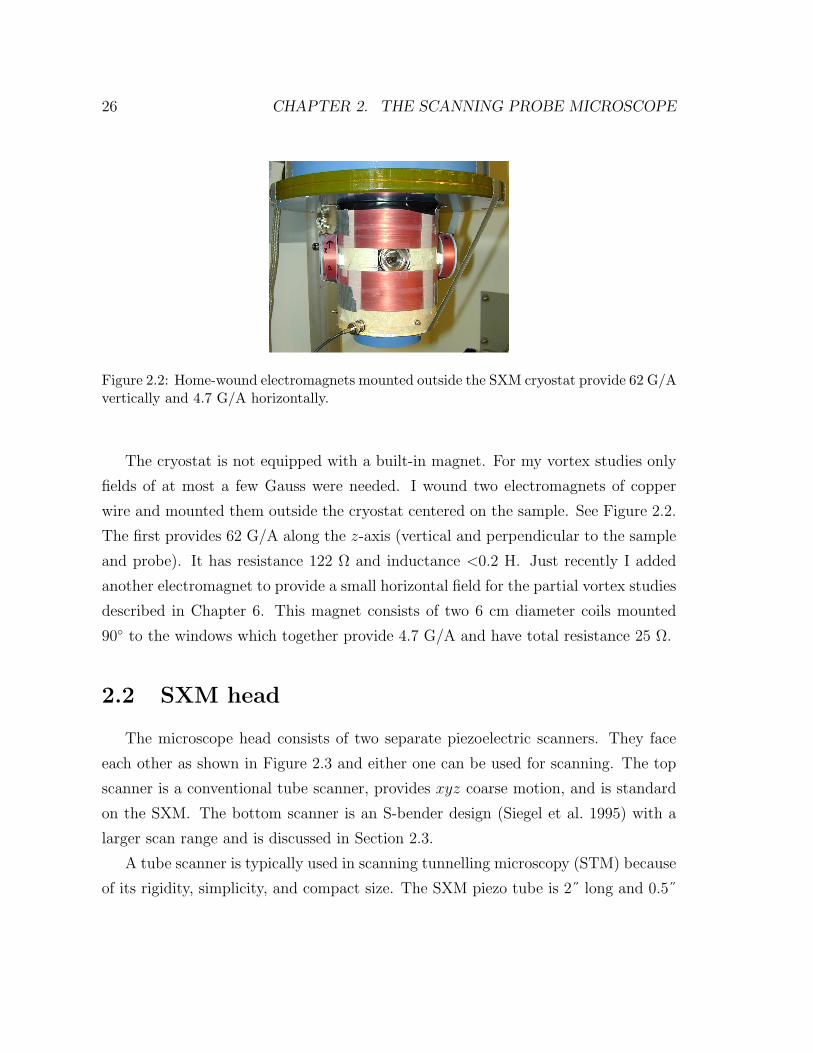
2.2 SXM head
The microscope head consists of two separate piezoelectric scanners. They face
each other as shown in Figure 2.3 and either one can be used for scanning. The top
scanner is a conventional tube scanner, provides xyz coarse motion, and is standard
on the SXM. The bottom scanner is an S-bender design (Siegel et al. 1995) with a
larger scan range and is discussed in Section 2.3.
A tube scanner is typically used in scanning tunnelling microscopy (STM) because
of its rigidity, simplicity, and compact size. The SXM piezo tube is 2˝ long and 0.5˝
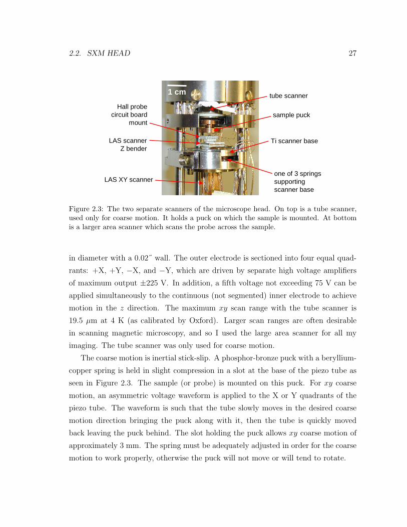
2.2. SXM HEAD 27
1 cm tube scanner
sample puck
Ti scanner base
one of 3 springs supporting scanner base
Hall probe circuit board
mount
LAS scanner Z bender
LAS XY scanner
Figure 2.3: The two separate scanners of the microscope head. On top is a tube scanner,used only for coarse motion. It holds a puck on which the sample is mounted. At bottomis a larger area scanner which scans the probe across the sample.
in diameter with a 0.02˝ wall. The outer electrode is sectioned into four equal quad-
rants: +X, +Y, −X, and −Y, which are driven by separate high voltage amplifiers
of maximum output ±225 V. In addition, a fifth voltage not exceeding 75 V can be
applied simultaneously to the continuous (not segmented) inner electrode to achieve
motion in the z direction. The maximum xy scan range with the tube scanner is
19.5 µm at 4 K (as calibrated by Oxford). Larger scan ranges are often desirable
in scanning magnetic microscopy, and so I used the large area scanner for all my
imaging. The tube scanner was only used for coarse motion.
The coarse motion is inertial stick-slip. A phosphor-bronze puck with a beryllium-
copper spring is held in slight compression in a slot at the base of the piezo tube as
seen in Figure 2.3. The sample (or probe) is mounted on this puck. For xy coarse
motion, an asymmetric voltage waveform is applied to the X or Y quadrants of the
piezo tube. The waveform is such that the tube slowly moves in the desired coarse
motion direction bringing the puck along with it, then the tube is quickly moved
back leaving the puck behind. The slot holding the puck allows xy coarse motion of
approximately 3 mm. The spring must be adequately adjusted in order for the coarse
motion to work properly, otherwise the puck will not move or will tend to rotate.
28 CHAPTER 2. THE SCANNING PROBE MICROSCOPE
At one point the stick-slip xy motion began to fail in first one and then two of the
four directions (±X & ±Y). Inspection of the piezo tube revealed that the electrodes
were flaking off the piezo quadrants. The electrodes had been coated with insulating
Kapton r© varnish and it seems that repeated thermal cycling cracked the varnish,
which then flaked off with the electrode attached. Rapid thermal changes >5 K/min
are bad for the piezos, however warming and cooling of the SXM was typically no
faster than 3 K/min. I replaced the tube scanner with a new assembly from Oxford
which intentionally had varnish only in essential locations, and I did not have further
problems with the xy coarse motion.
For the z coarse motion, the entire tube scanner rides up and down on three hollow
quartz cylinders each connected to a piezo stack. The asymmetric voltage waveform
is applied to these piezo stacks to achieve inertial stick-slip motion of the whole scan
tube assembly on which the sample (or probe) is mounted. The full z range is nearly
1 cm, however at low temperature I found that the z coarse motion worked reliably
only for a restricted range. For this reason it was necessary to approach the sample
to the probe first at around 90 K before cooling to lower temperatures to ensure that
the probe was within range.
Near the sample puck are sockets to make electrical connections to the sample
and probe. These sockets are attached to 4 shielded twisted pairs (8 wires total)
and 2 coaxes that extend to the top of the rod. These connections, as well as the
piezo voltage connections and the leads to the Cernox thermometer, exit the sample
chamber through vacuum tight connectors on top of the rod. I also wired the rod for
6 additional sample/probe connections. These wires are in unshielded twisted pairs
to the top of the rod where they exit through the thermometer connector and utilize
extra wires in the temperature control cable. The wires are not well shielded or in
twisted pairs outside of the sample space, but are adequate for some applications
when additional connections are needed.
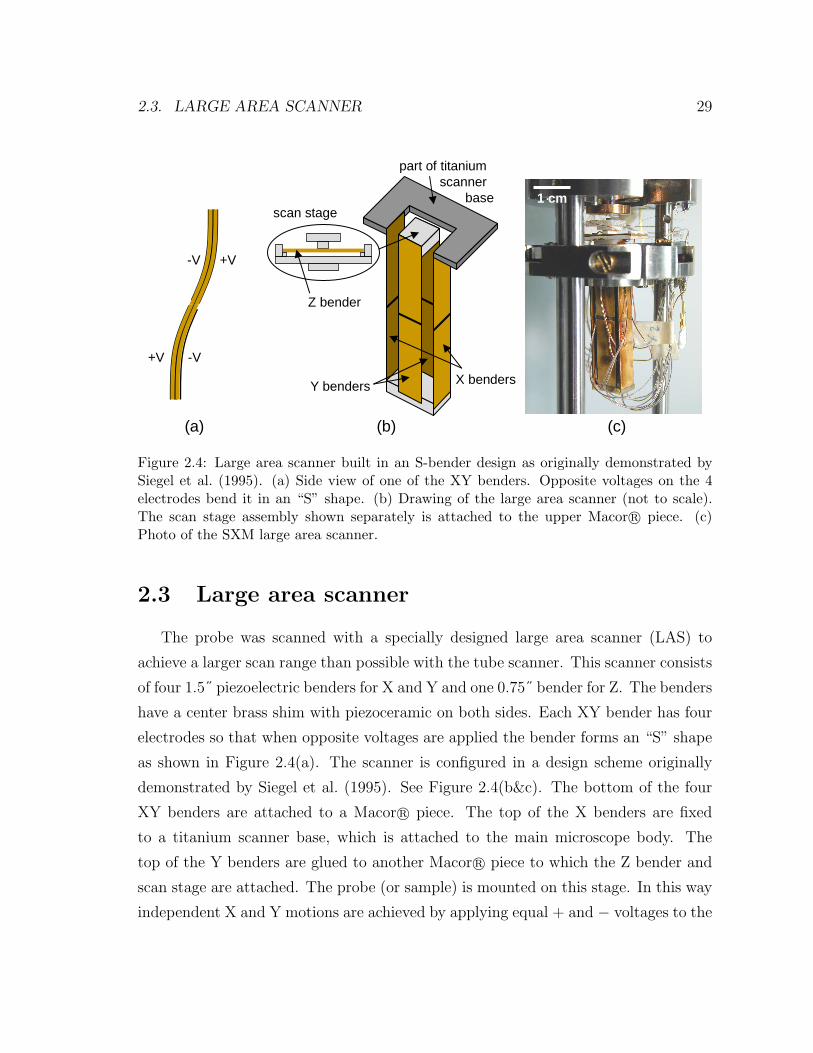
2.3. LARGE AREA SCANNER 29
1 cm
-V
-V
+V
+V
Y benders X benders
part of titaniumscanner
base
(a) (b) (c)
scan stage
Z bender
Figure 2.4: Large area scanner built in an S-bender design as originally demonstrated bySiegel et al. (1995). (a) Side view of one of the XY benders. Opposite voltages on the 4electrodes bend it in an “S” shape. (b) Drawing of the large area scanner (not to scale).The scan stage assembly shown separately is attached to the upper Macor r© piece. (c)Photo of the SXM large area scanner.
2.3 Large area scanner
The probe was scanned with a specially designed large area scanner (LAS) to
achieve a larger scan range than possible with the tube scanner. This scanner consists
of four 1.5˝ piezoelectric benders for X and Y and one 0.75˝ bender for Z. The benders
have a center brass shim with piezoceramic on both sides. Each XY bender has four
electrodes so that when opposite voltages are applied the bender forms an “S” shape
as shown in Figure 2.4(a). The scanner is configured in a design scheme originally
demonstrated by Siegel et al. (1995). See Figure 2.4(b&c). The bottom of the four
XY benders are attached to a Macor r© piece. The top of the X benders are fixed
to a titanium scanner base, which is attached to the main microscope body. The
top of the Y benders are glued to another Macor r© piece to which the Z bender and
scan stage are attached. The probe (or sample) is mounted on this stage. In this way
independent X and Y motions are achieved by applying equal + and − voltages to the
30 CHAPTER 2. THE SCANNING PROBE MICROSCOPE
X or Y benders. The Z bender has two electrodes and is mounted horizontally with
both ends fixed. One side is grounded while the other is supplied with a maximum
of ±150 V. This allows independent Z motion. A 5 mm × 5 mm Macor r© stage is
mounted on the Z bender and the probe setup is glued to this stage.
The titanium plate to which the X benders are fixed is attached to the main mi-
croscope body by three springs. This plate can be tilted by means of three set screws
which control the spring extensions in order to adjust the probe-sample alignment.
At room temperature the LAS moves ∼0.6 µm/V in X and Y, where the voltage is
the voltage difference between the + and − electrodes. At 4 K the motion decreases
to ∼0.11 µm/V. The scan range at 4 K is limited by the voltage difference at which
the piezos begin to arc. I found this to happen for scans larger than 60 µm× 60 µm,
or a voltage difference >270 V (±135 V on the opposite electrodes). When pumping
He through the sample space with the SOGEVAC pump, the pressure as measured by
a gauge near the pump is several Torr, which I’ve been told is a bad helium pressure
for arcing. A larger scan range could be achieved by changing to longer benders.
2.3.1 Piezo resonances and vibrational noise
I studied the resonant frequencies and vibrational noise of the LAS at room tem-
perature early on in my research. These measurements were made with the microscope
in the cryostat and the cryostat suspended by bungee cords as when scanning, but
the pump was not connected. The lowest mode of the scanner is ∼40 Hz.
The resonances were studied by mounting pieces of silicon wafer to the scan stage
parallel to the X and Y piezo benders. A Polytec Series 3000 vibrometer was used
to bounce a laser off the Si to measure its velocity. The + electrodes of the X and Y
benders were driven, one direction at a time, with a small sinusoidal voltage of 10 mV
at frequency f , and the velocity response at f was recorded. This measurement was
made for a sweep of f to give the scanner response as a function of frequency. The
velocity response measured by the vibrometer was converted to amplitude by dividing
by 2πf . The response of the LAS in µm/V is shown as a function of drive frequency in
Figure 2.5. The first mode is just below 40 Hz for both X and Y, and a large resonant
2.3. LARGE AREA SCANNER 31
0 50 100 150 200 250 300 350 40010
−2
10−1
100
101
Frequency (Hz)
Pie
zo r
espo
nse
(µm
/V)
XY
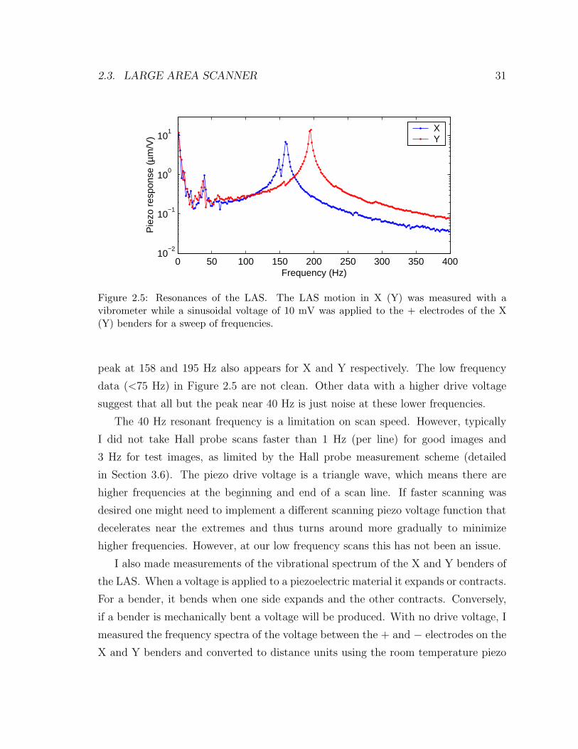
Figure 2.5: Resonances of the LAS. The LAS motion in X (Y) was measured with avibrometer while a sinusoidal voltage of 10 mV was applied to the + electrodes of the X(Y) benders for a sweep of frequencies.
peak at 158 and 195 Hz also appears for X and Y respectively. The low frequency
data (<75 Hz) in Figure 2.5 are not clean. Other data with a higher drive voltage
suggest that all but the peak near 40 Hz is just noise at these lower frequencies.
The 40 Hz resonant frequency is a limitation on scan speed. However, typically
I did not take Hall probe scans faster than 1 Hz (per line) for good images and
3 Hz for test images, as limited by the Hall probe measurement scheme (detailed
in Section 3.6). The piezo drive voltage is a triangle wave, which means there are
higher frequencies at the beginning and end of a scan line. If faster scanning was
desired one might need to implement a different scanning piezo voltage function that
decelerates near the extremes and thus turns around more gradually to minimize
higher frequencies. However, at our low frequency scans this has not been an issue.
I also made measurements of the vibrational spectrum of the X and Y benders of
the LAS. When a voltage is applied to a piezoelectric material it expands or contracts.
For a bender, it bends when one side expands and the other contracts. Conversely,
if a bender is mechanically bent a voltage will be produced. With no drive voltage, I
measured the frequency spectra of the voltage between the + and − electrodes on the
X and Y benders and converted to distance units using the room temperature piezo
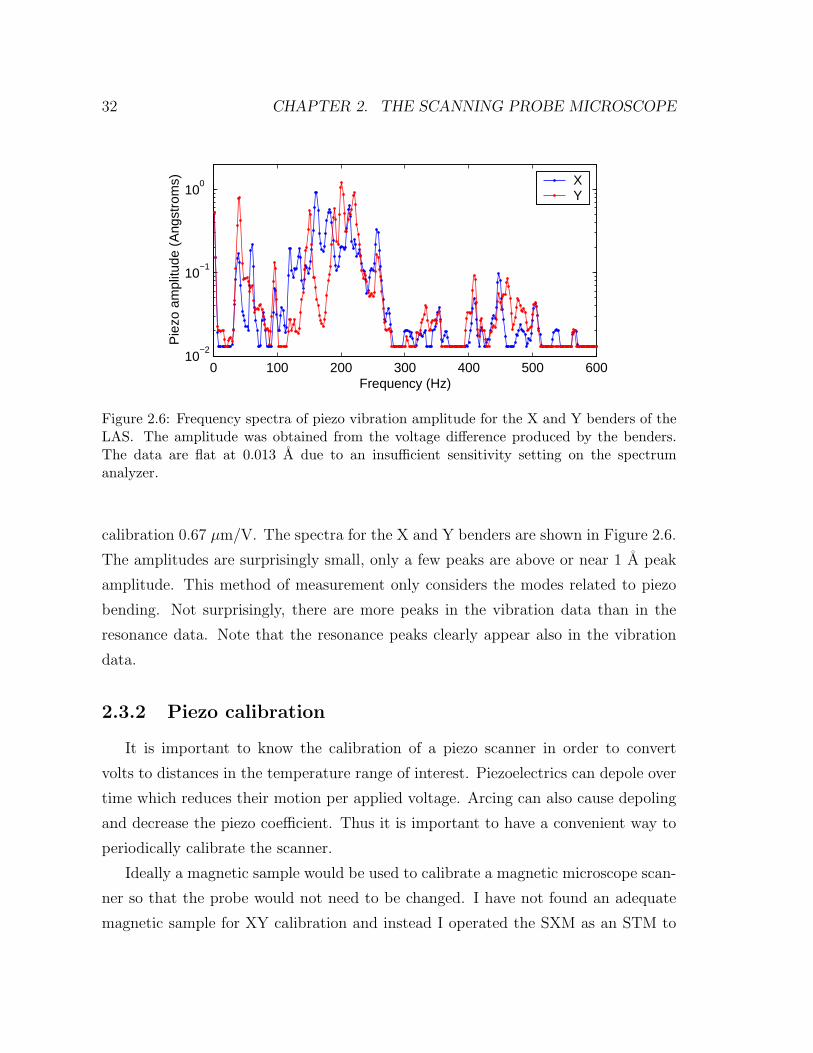
32 CHAPTER 2. THE SCANNING PROBE MICROSCOPE
0 100 200 300 400 500 60010
−2
10−1
100
Frequency (Hz)
Pie
zo a
mpl
itude
(A
ngst
rom
s) XY
Figure 2.6: Frequency spectra of piezo vibration amplitude for the X and Y benders of theLAS. The amplitude was obtained from the voltage difference produced by the benders.The data are flat at 0.013 A due to an insufficient sensitivity setting on the spectrumanalyzer.
calibration 0.67 µm/V. The spectra for the X and Y benders are shown in Figure 2.6.
The amplitudes are surprisingly small, only a few peaks are above or near 1 A peak
amplitude. This method of measurement only considers the modes related to piezo
bending. Not surprisingly, there are more peaks in the vibration data than in the
resonance data. Note that the resonance peaks clearly appear also in the vibration
data.
2.3.2 Piezo calibration
It is important to know the calibration of a piezo scanner in order to convert
volts to distances in the temperature range of interest. Piezoelectrics can depole over
time which reduces their motion per applied voltage. Arcing can also cause depoling
and decrease the piezo coefficient. Thus it is important to have a convenient way to
periodically calibrate the scanner.
Ideally a magnetic sample would be used to calibrate a magnetic microscope scan-
ner so that the probe would not need to be changed. I have not found an adequate
magnetic sample for XY calibration and instead I operated the SXM as an STM to
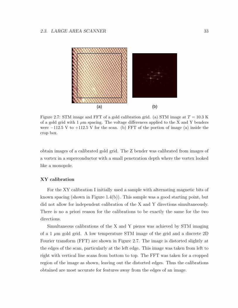
2.3. LARGE AREA SCANNER 33
(a) (b)
Figure 2.7: STM image and FFT of a gold calibration grid. (a) STM image at T = 10.3 Kof a gold grid with 1 µm spacing. The voltage differences applied to the X and Y benderswere −112.5 V to +112.5 V for the scan. (b) FFT of the portion of image (a) inside thecrop box.
obtain images of a calibrated gold grid. The Z bender was calibrated from images of
a vortex in a superconductor with a small penetration depth where the vortex looked
like a monopole.
XY calibration
For the XY calibration I initially used a sample with alternating magnetic bits of
known spacing (shown in Figure 1.4(b)). This sample was a good starting point, but
did not allow for independent calibration of the X and Y directions simultaneously.
There is no a priori reason for the calibrations to be exactly the same for the two
directions.
Simultaneous calibrations of the X and Y piezos was achieved by STM imaging
of a 1 µm gold grid. A low temperature STM image of the grid and a discrete 2D
Fourier transform (FFT) are shown in Figure 2.7. The image is distorted slightly at
the edges of the scan, particularly at the left edge. This image was taken from left to
right with vertical line scans from bottom to top. The FFT was taken for a cropped
region of the image as shown, leaving out the distorted edges. Thus the calibrations
obtained are most accurate for features away from the edges of an image.
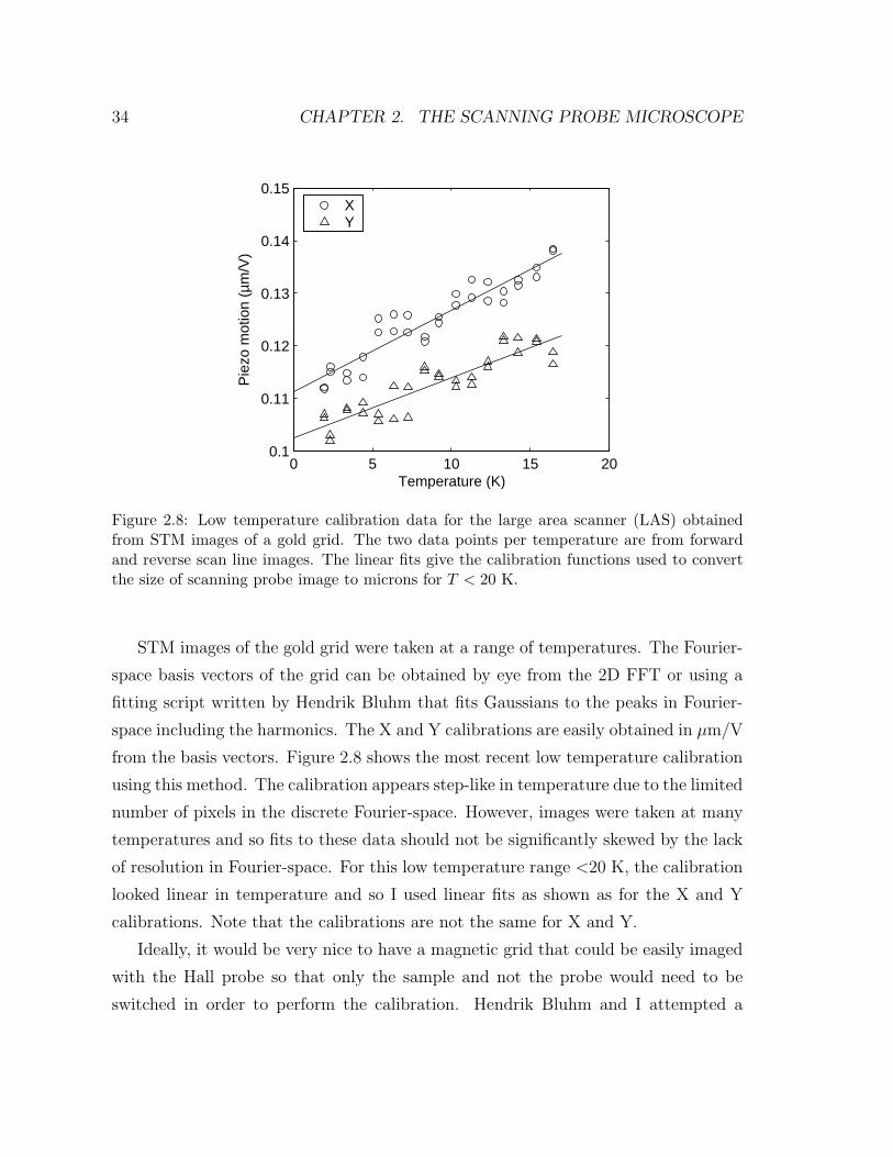
34 CHAPTER 2. THE SCANNING PROBE MICROSCOPE
0 5 10 15 200.1
0.11
0.12
0.13
0.14
0.15
Temperature (K)
Pie
zo m
otio
n (µ
m/V
)
XY
Figure 2.8: Low temperature calibration data for the large area scanner (LAS) obtainedfrom STM images of a gold grid. The two data points per temperature are from forwardand reverse scan line images. The linear fits give the calibration functions used to convertthe size of scanning probe image to microns for T < 20 K.
STM images of the gold grid were taken at a range of temperatures. The Fourier-
space basis vectors of the grid can be obtained by eye from the 2D FFT or using a
fitting script written by Hendrik Bluhm that fits Gaussians to the peaks in Fourier-
space including the harmonics. The X and Y calibrations are easily obtained in µm/V
from the basis vectors. Figure 2.8 shows the most recent low temperature calibration
using this method. The calibration appears step-like in temperature due to the limited
number of pixels in the discrete Fourier-space. However, images were taken at many
temperatures and so fits to these data should not be significantly skewed by the lack
of resolution in Fourier-space. For this low temperature range <20 K, the calibration
looked linear in temperature and so I used linear fits as shown as for the X and Y
calibrations. Note that the calibrations are not the same for X and Y.
Ideally, it would be very nice to have a magnetic grid that could be easily imaged
with the Hall probe so that only the sample and not the probe would need to be
switched in order to perform the calibration. Hendrik Bluhm and I attempted a
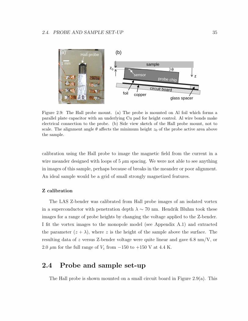
2.4. PROBE AND SAMPLE SET-UP 35
θ
probe chip
(
sensor
foil
z
sample
circuit boardcopper
z0
glass spacer
Hall probe(a) (b)
1 mm
Figure 2.9: The Hall probe mount. (a) The probe is mounted on Al foil which forms aparallel plate capacitor with an underlying Cu pad for height control. Al wire bonds makeelectrical connection to the probe. (b) Side view sketch of the Hall probe mount, not toscale. The alignment angle θ affects the minimum height z0 of the probe active area abovethe sample.
calibration using the Hall probe to image the magnetic field from the current in a
wire meander designed with loops of 5 µm spacing. We were not able to see anything
in images of this sample, perhaps because of breaks in the meander or poor alignment.
An ideal sample would be a grid of small strongly magnetized features.
Z calibration
The LAS Z-bender was calibrated from Hall probe images of an isolated vortex
in a superconductor with penetration depth λ ∼ 70 nm. Hendrik Bluhm took these
images for a range of probe heights by changing the voltage applied to the Z-bender.
I fit the vortex images to the monopole model (see Appendix A.1) and extracted
the parameter (z + λ), where z is the height of the sample above the surface. The
resulting data of z versus Z-bender voltage were quite linear and gave 6.8 nm/V, or
2.0 µm for the full range of Vz from −150 to +150 V at 4.4 K.
2.4 Probe and sample set-up
The Hall probe is shown mounted on a small circuit board in Figure 2.9(a). This
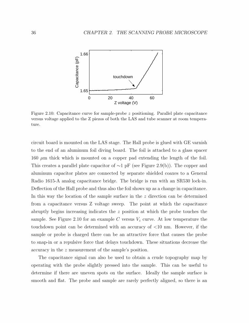
36 CHAPTER 2. THE SCANNING PROBE MICROSCOPE
0 20 40 60
1.65
1.66
Cap
acita
nce
(pF
)
Z voltage (V)
touchdown
Figure 2.10: Capacitance curve for sample-probe z positioning. Parallel plate capacitanceversus voltage applied to the Z piezos of both the LAS and tube scanner at room tempera-ture.
circuit board is mounted on the LAS stage. The Hall probe is glued with GE varnish
to the end of an aluminum foil diving board. The foil is attached to a glass spacer
160 µm thick which is mounted on a copper pad extending the length of the foil.
This creates a parallel plate capacitor of ∼1 pF (see Figure 2.9(b)). The copper and
aluminum capacitor plates are connected by separate shielded coaxes to a General
Radio 1615-A analog capacitance bridge. The bridge is run with an SR530 lock-in.
Deflection of the Hall probe and thus also the foil shows up as a change in capacitance.
In this way the location of the sample surface in the z direction can be determined
from a capacitance versus Z voltage sweep. The point at which the capacitance
abruptly begins increasing indicates the z position at which the probe touches the
sample. See Figure 2.10 for an example C versus Vz curve. At low temperature the
touchdown point can be determined with an accuracy of <10 nm. However, if the
sample or probe is charged there can be an attractive force that causes the probe
to snap-in or a repulsive force that delays touchdown. These situations decrease the
accuracy in the z measurement of the sample’s position.
The capacitance signal can also be used to obtain a crude topography map by
operating with the probe slightly pressed into the sample. This can be useful to
determine if there are uneven spots on the surface. Ideally the sample surface is
smooth and flat. The probe and sample are rarely perfectly aligned, so there is an
2.4. PROBE AND SAMPLE SET-UP 37
angle between the scan plane of the probe and the plane of the sample surface. This is
compensated by a home-built analog circuit box that gives a Z voltage corresponding
to a plane as a function of X and Y piezo voltages. The slopes mx and my of the
plane are controlled by potentiometer knobs and the values are obtained by checking
the touchdown points on the surface for 3 or more locations within the image area.
A drawback of the way the probe and sample are mounted is that it is not possible
to fine adjust both the angle of the probe and the angle of the LAS scan plane to
the sample surface. This is because the probe rather than the sample is attached to
the scanner, and the angle between the probe and scan plane is not fine tunable (it is
determined by the angle of the aluminum foil). The three tilt screws for the LAS do
allow fine adjustments of the scan plane, but if it is adjusted parallel to the sample
surface often the angle of the Hall probe to the sample is too large or too small. One
solution would be to mount the probe on the sample puck which is held by the tube
scanner and kept stationary, and mount the sample on the LAS stage. This has two
major drawbacks which outweigh the alignment issue. First, it is not nearly as easy
to switch samples as when the sample is mounted on the puck. Second and more
fundamental is that this arrangement would scan the sample rather than the probe.
For many samples this would not be an issue, but the vortices observed in the very
underdoped YBCO studies were sometimes rather mobile, especially the “partial”
ones discussed in Chapter 6, and vortex motion might be induced by scanning the
sample.
Electrical connection is made to the Hall probe with aluminum wire bonds from
copper pads on the circuit board (Figure 2.9(a)) to the end of the Hall probe contact
pads furthest from the Hall probe tip. For large samples it is important to bond the
wires as far from the tip as possible since the 0.001˝ wire width is the limiting factor
on the angle between the probe and sample. Many of the YBa2Cu3O6+x crystals were
smaller than the Hall probe and thus the wire bonds could hang off the edge of the
sample and were not an issue. Typically I polished the aluminum foil on which the
probe was mounted to make it thinner to reduce its spring constant and minimize the
force between the probe and sample when touching. However, it became apparent
that the wire bonds to the Hall probe were the most significant contribution to the
38 CHAPTER 2. THE SCANNING PROBE MICROSCOPE
spring constant. Thin copper wires were soldered to the circuit board pads and
connected on the other end to the sockets in the microscope. The wire chosen was
the thinnest reasonable to work with to ensure that the wires would not hinder the
scanning of the probe.
2.5 Scanning hardware and software
The scanning and coarse motion was done with the commercial TOPS 3 System
from Oxford Instruments.2 Initially I also used the TOPS hardware and software
and the attached computer for data acquisition. I later switched to taking data on a
separate computer because TOPS caused noise problems with the Hall probe.
The TOPS system has 5 high voltage amplifiers: +X, −X, +Y, −Y, and Z. The
four XY amplifiers have full range ±225 V and the Z amplifier is set for ±150 V
but the maximum amplitude can be adjusted. (I recently increased this Z amplitude
from ±75 V in order to enable larger area scans without maxing out the fly-in-
plane.) The coarse motion waveforms are also produced and controlled by the TOPS
system. TOPS has 8 differential analog-to-digital inputs for recording the sensor
signal. Brian Gardner wrote a nice program to input images from the TOPS data
format to MABLAB r©.
I stopped acquiring data with the TOPS system after noticing scan related noise in
Hall probe images in 2002. See Figure 2.11. The noise was systematic, as it appeared
as steps in the signal at fractions of the scan size, the most prominent at 14, 1
2, and 3
4
of the scan line. To eliminate the intrinsic 1/f -like noise of the Hall probe, images
are taken quickly and averaged together. However, averaging just brought out this
TOPS scan step noise. The noise was also subtly present in early images taken with
a 2 µm Hall probe, but back then the data taking was not yet optimized and other
noise dominated. I was never able to pinpoint the cause of this step noise, though it
seemed that there was a significant grounding problem with the A/D inputs to the
TOPS system. Changing the gain did not change the signal-to-noise, and putting
an isolation amplifier between the Hall probe output (from a lock-in) and the A/D
2The TOPS system is no longer produced.
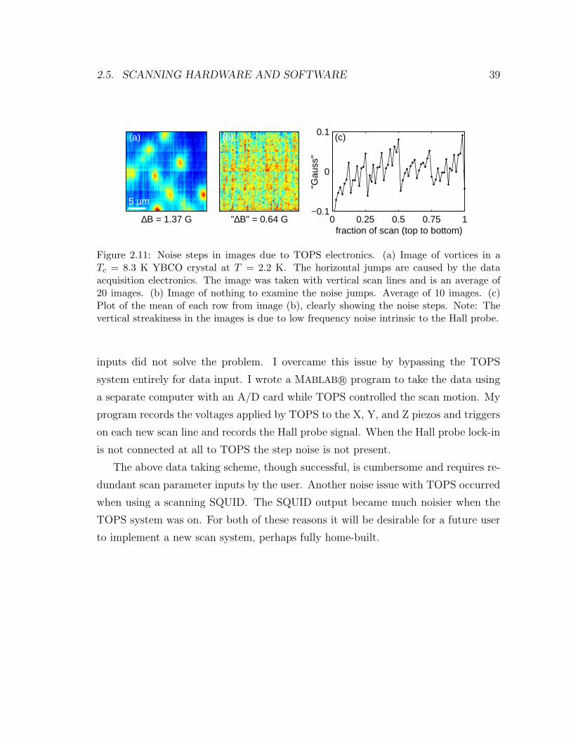
2.5. SCANNING HARDWARE AND SOFTWARE 39
∆B = 1.37 G
5 µm
(a)
"∆B" = 0.64 G
(b)
0 0.25 0.5 0.75 1−0.1
0
0.1
fraction of scan (top to bottom)
"Gau
ss"
(c)
Figure 2.11: Noise steps in images due to TOPS electronics. (a) Image of vortices in aTc = 8.3 K YBCO crystal at T = 2.2 K. The horizontal jumps are caused by the dataacquisition electronics. The image was taken with vertical scan lines and is an average of20 images. (b) Image of nothing to examine the noise jumps. Average of 10 images. (c)Plot of the mean of each row from image (b), clearly showing the noise steps. Note: Thevertical streakiness in the images is due to low frequency noise intrinsic to the Hall probe.
inputs did not solve the problem. I overcame this issue by bypassing the TOPS
system entirely for data input. I wrote a MABLAB r© program to take the data using
a separate computer with an A/D card while TOPS controlled the scan motion. My
program records the voltages applied by TOPS to the X, Y, and Z piezos and triggers
on each new scan line and records the Hall probe signal. When the Hall probe lock-in
is not connected at all to TOPS the step noise is not present.
The above data taking scheme, though successful, is cumbersome and requires re-
dundant scan parameter inputs by the user. Another noise issue with TOPS occurred
when using a scanning SQUID. The SQUID output became much noisier when the
TOPS system was on. For both of these reasons it will be desirable for a future user
to implement a new scan system, perhaps fully home-built.
40 CHAPTER 2. THE SCANNING PROBE MICROSCOPE
Chapter 3
Submicron scanning Hall probes
In addition to implementing the scanning Hall probe microscope (Chapter 2) and
using it for vortex imaging studies in very underdoped YBa2Cu3O6+x (Chapters 4–6),
I also fabricated submicron scanning Hall probes from GaAs/AlGaAs two-dimensional
electron gas (2DEG). The smallest probes from this fabrication were 0.5 µm litho-
graphically, a factor of four smaller than the previous probes I was using, and enabled
measurements of the apparent vortex size (Chapter 5) and partial vortex imaging
(Chapter 6) in the YBCO.
There are numerous qualities to consider when selecting and developing a scanning
magnetic sensor: spatial resolution, magnetic field sensitivity, ease of interpretation,
extent of sample preparation, temperature and field range, and dynamic speed. The
three sensors used in the Moler Lab (MFM, SQUIDs, and Hall probes) were compared
in Section 1.1.1 and Table 1.1. The main advantages of Hall probes are that they
directly measure the magnetic field, can be made at least as small as ∼100 nm, are
non-invasive, and operate over a large temperature range (0–300 K).
This chapter gives a brief review of the Hall effect, details my fabrication of
0.5–2 µm Hall probes with gates, and lastly describes noise measurements made on
these and later probes. My probes improved the spatial resolution of the scanning
Hall probe microscope at least four-fold, and the addition of a grounded gate over
the active area improved image quality by screening out local electric fields. The
noise studies of scanning Hall probes ranging in size from 0.13 µm to 10 µm show
that field sensitivity decreased for smaller probes, but flux sensitivity increased. This
41
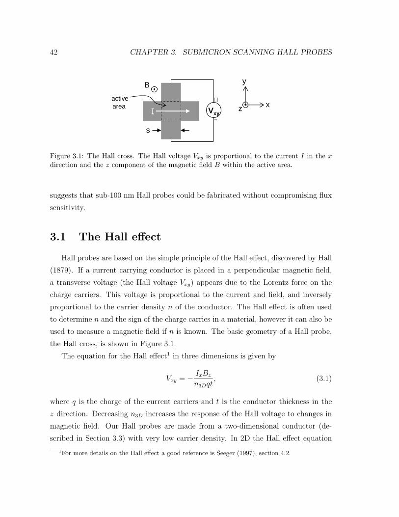
42 CHAPTER 3. SUBMICRON SCANNING HALL PROBES
I
B
s
x
y
zVxy
activearea
+
−
Figure 3.1: The Hall cross. The Hall voltage Vxy is proportional to the current I in the xdirection and the z component of the magnetic field B within the active area.
suggests that sub-100 nm Hall probes could be fabricated without compromising flux
sensitivity.
3.1 The Hall effect
Hall probes are based on the simple principle of the Hall effect, discovered by Hall
(1879). If a current carrying conductor is placed in a perpendicular magnetic field,
a transverse voltage (the Hall voltage Vxy) appears due to the Lorentz force on the
charge carriers. This voltage is proportional to the current and field, and inversely
proportional to the carrier density n of the conductor. The Hall effect is often used
to determine n and the sign of the charge carries in a material, however it can also be
used to measure a magnetic field if n is known. The basic geometry of a Hall probe,
the Hall cross, is shown in Figure 3.1.
The equation for the Hall effect1 in three dimensions is given by
Vxy = − IxBz
n3Dqt, (3.1)
where q is the charge of the current carriers and t is the conductor thickness in the
z direction. Decreasing n3D increases the response of the Hall voltage to changes in
magnetic field. Our Hall probes are made from a two-dimensional conductor (de-
scribed in Section 3.3) with very low carrier density. In 2D the Hall effect equation
1For more details on the Hall effect a good reference is Seeger (1997), section 4.2.
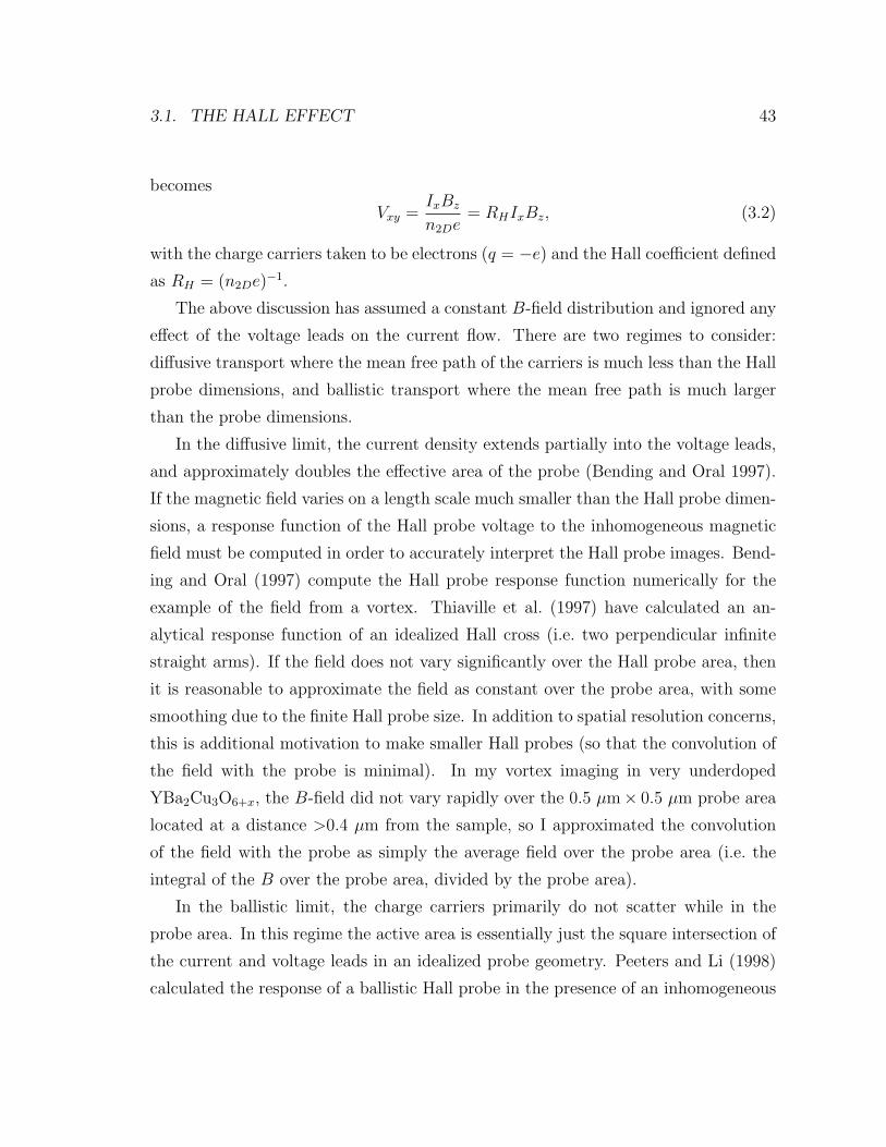
3.1. THE HALL EFFECT 43
becomes
Vxy =IxBz
n2De= RHIxBz, (3.2)
with the charge carriers taken to be electrons (q = −e) and the Hall coefficient defined
as RH = (n2De)−1.
The above discussion has assumed a constant B-field distribution and ignored any
effect of the voltage leads on the current flow. There are two regimes to consider:
diffusive transport where the mean free path of the carriers is much less than the Hall
probe dimensions, and ballistic transport where the mean free path is much larger
than the probe dimensions.
In the diffusive limit, the current density extends partially into the voltage leads,
and approximately doubles the effective area of the probe (Bending and Oral 1997).
If the magnetic field varies on a length scale much smaller than the Hall probe dimen-
sions, a response function of the Hall probe voltage to the inhomogeneous magnetic
field must be computed in order to accurately interpret the Hall probe images. Bend-
ing and Oral (1997) compute the Hall probe response function numerically for the
example of the field from a vortex. Thiaville et al. (1997) have calculated an an-
alytical response function of an idealized Hall cross (i.e. two perpendicular infinite
straight arms). If the field does not vary significantly over the Hall probe area, then
it is reasonable to approximate the field as constant over the probe area, with some
smoothing due to the finite Hall probe size. In addition to spatial resolution concerns,
this is additional motivation to make smaller Hall probes (so that the convolution of
the field with the probe is minimal). In my vortex imaging in very underdoped
YBa2Cu3O6+x, the B-field did not vary rapidly over the 0.5 µm× 0.5 µm probe area
located at a distance >0.4 µm from the sample, so I approximated the convolution
of the field with the probe as simply the average field over the probe area (i.e. the
integral of the B over the probe area, divided by the probe area).
In the ballistic limit, the charge carriers primarily do not scatter while in the
probe area. In this regime the active area is essentially just the square intersection of
the current and voltage leads in an idealized probe geometry. Peeters and Li (1998)
calculated the response of a ballistic Hall probe in the presence of an inhomogeneous
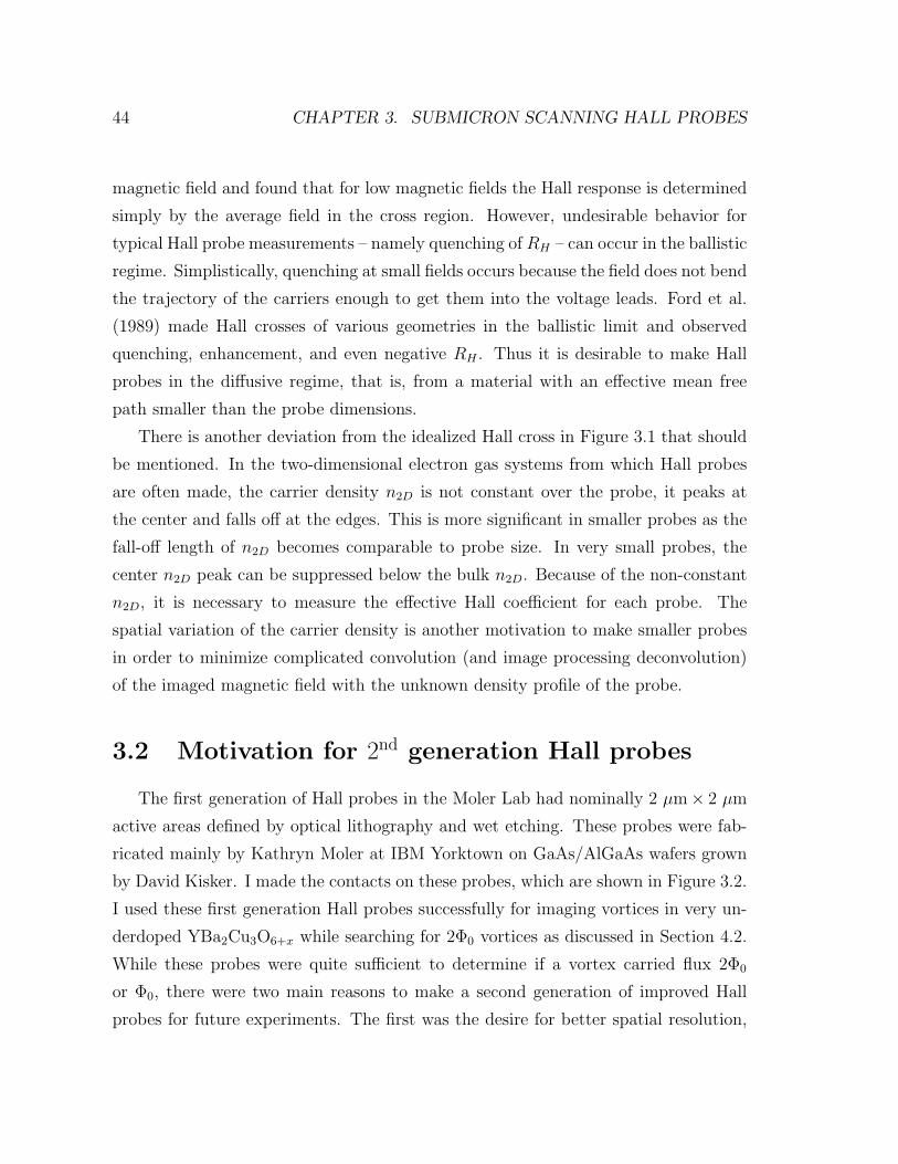
44 CHAPTER 3. SUBMICRON SCANNING HALL PROBES
magnetic field and found that for low magnetic fields the Hall response is determined
simply by the average field in the cross region. However, undesirable behavior for
typical Hall probe measurements – namely quenching of RH – can occur in the ballistic
regime. Simplistically, quenching at small fields occurs because the field does not bend
the trajectory of the carriers enough to get them into the voltage leads. Ford et al.
(1989) made Hall crosses of various geometries in the ballistic limit and observed
quenching, enhancement, and even negative RH . Thus it is desirable to make Hall
probes in the diffusive regime, that is, from a material with an effective mean free
path smaller than the probe dimensions.
There is another deviation from the idealized Hall cross in Figure 3.1 that should
be mentioned. In the two-dimensional electron gas systems from which Hall probes
are often made, the carrier density n2D is not constant over the probe, it peaks at
the center and falls off at the edges. This is more significant in smaller probes as the
fall-off length of n2D becomes comparable to probe size. In very small probes, the
center n2D peak can be suppressed below the bulk n2D. Because of the non-constant
n2D, it is necessary to measure the effective Hall coefficient for each probe. The
spatial variation of the carrier density is another motivation to make smaller probes
in order to minimize complicated convolution (and image processing deconvolution)
of the imaged magnetic field with the unknown density profile of the probe.
3.2 Motivation for 2nd generation Hall probes
The first generation of Hall probes in the Moler Lab had nominally 2 µm× 2 µm
active areas defined by optical lithography and wet etching. These probes were fab-
ricated mainly by Kathryn Moler at IBM Yorktown on GaAs/AlGaAs wafers grown
by David Kisker. I made the contacts on these probes, which are shown in Figure 3.2.
I used these first generation Hall probes successfully for imaging vortices in very un-
derdoped YBa2Cu3O6+x while searching for 2Φ0 vortices as discussed in Section 4.2.
While these probes were quite sufficient to determine if a vortex carried flux 2Φ0
or Φ0, there were two main reasons to make a second generation of improved Hall
probes for future experiments. The first was the desire for better spatial resolution,
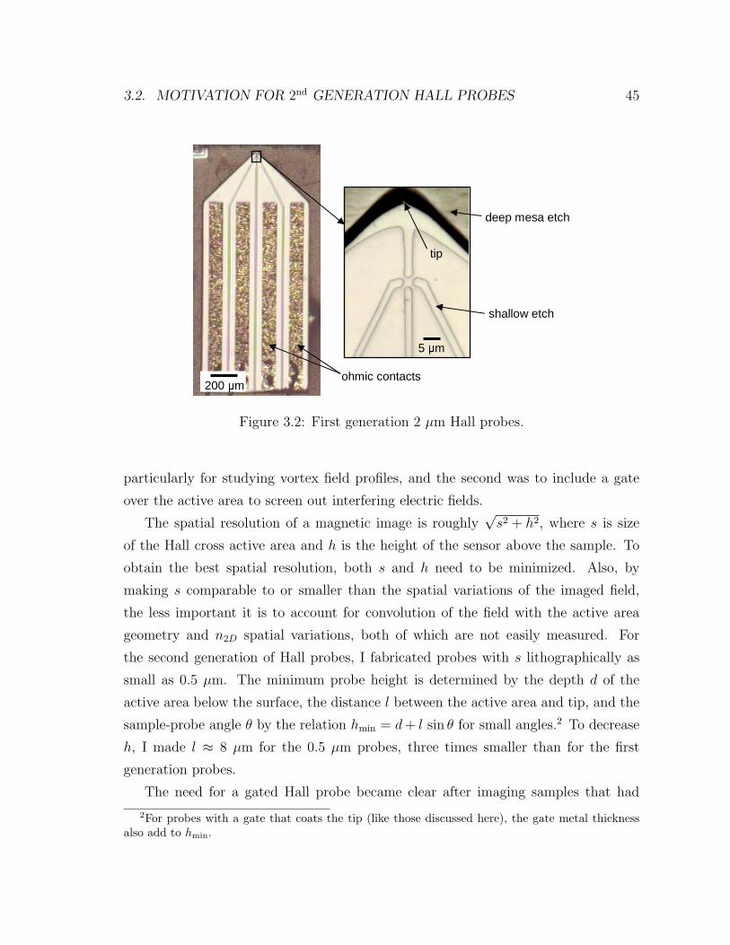
3.2. MOTIVATION FOR 2nd GENERATION HALL PROBES 45
5 m
shallow etch
deep mesa etch
ohmic contacts200 m
tip
Figure 3.2: First generation 2 µm Hall probes.
particularly for studying vortex field profiles, and the second was to include a gate
over the active area to screen out interfering electric fields.
The spatial resolution of a magnetic image is roughly√
s2 + h2, where s is size
of the Hall cross active area and h is the height of the sensor above the sample. To
obtain the best spatial resolution, both s and h need to be minimized. Also, by
making s comparable to or smaller than the spatial variations of the imaged field,
the less important it is to account for convolution of the field with the active area
geometry and n2D spatial variations, both of which are not easily measured. For
the second generation of Hall probes, I fabricated probes with s lithographically as
small as 0.5 µm. The minimum probe height is determined by the depth d of the
active area below the surface, the distance l between the active area and tip, and the
sample-probe angle θ by the relation hmin = d + l sin θ for small angles.2 To decrease
h, I made l ≈ 8 µm for the 0.5 µm probes, three times smaller than for the first
generation probes.
The need for a gated Hall probe became clear after imaging samples that had
2For probes with a gate that coats the tip (like those discussed here), the gate metal thicknessalso add to hmin.
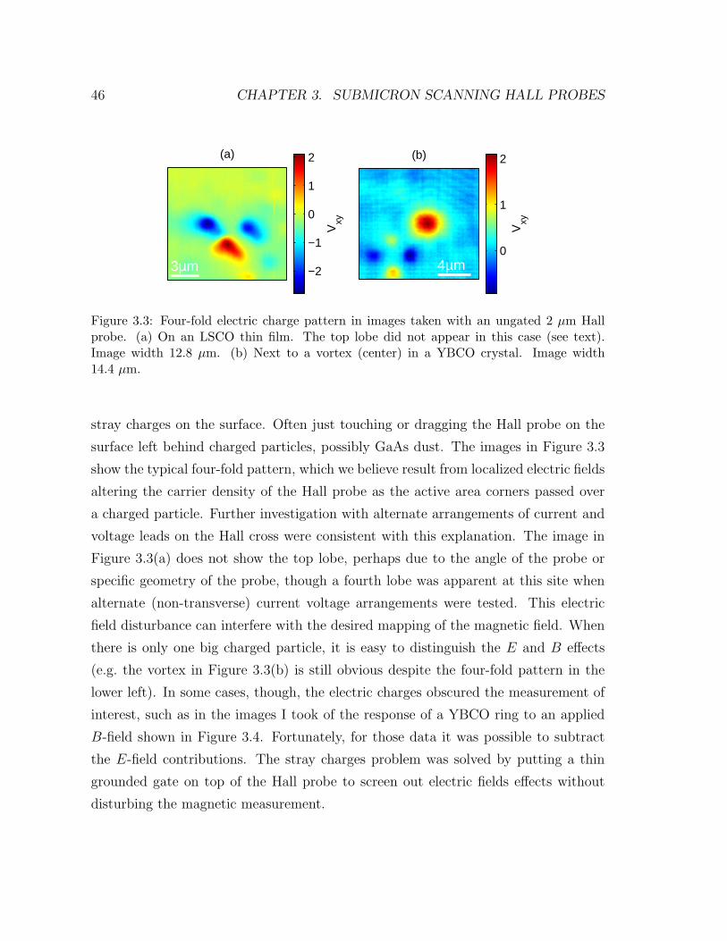
46 CHAPTER 3. SUBMICRON SCANNING HALL PROBES
Vxy
−2
−1
0
1
2 (a)
3µm
Vxy
0
1
2(b)
4µm
Figure 3.3: Four-fold electric charge pattern in images taken with an ungated 2 µm Hallprobe. (a) On an LSCO thin film. The top lobe did not appear in this case (see text).Image width 12.8 µm. (b) Next to a vortex (center) in a YBCO crystal. Image width14.4 µm.
stray charges on the surface. Often just touching or dragging the Hall probe on the
surface left behind charged particles, possibly GaAs dust. The images in Figure 3.3
show the typical four-fold pattern, which we believe result from localized electric fields
altering the carrier density of the Hall probe as the active area corners passed over
a charged particle. Further investigation with alternate arrangements of current and
voltage leads on the Hall cross were consistent with this explanation. The image in
Figure 3.3(a) does not show the top lobe, perhaps due to the angle of the probe or
specific geometry of the probe, though a fourth lobe was apparent at this site when
alternate (non-transverse) current voltage arrangements were tested. This electric
field disturbance can interfere with the desired mapping of the magnetic field. When
there is only one big charged particle, it is easy to distinguish the E and B effects
(e.g. the vortex in Figure 3.3(b) is still obvious despite the four-fold pattern in the
lower left). In some cases, though, the electric charges obscured the measurement of
interest, such as in the images I took of the response of a YBCO ring to an applied
B-field shown in Figure 3.4. Fortunately, for those data it was possible to subtract
the E-field contributions. The stray charges problem was solved by putting a thin
grounded gate on top of the Hall probe to screen out electric fields effects without
disturbing the magnetic measurement.
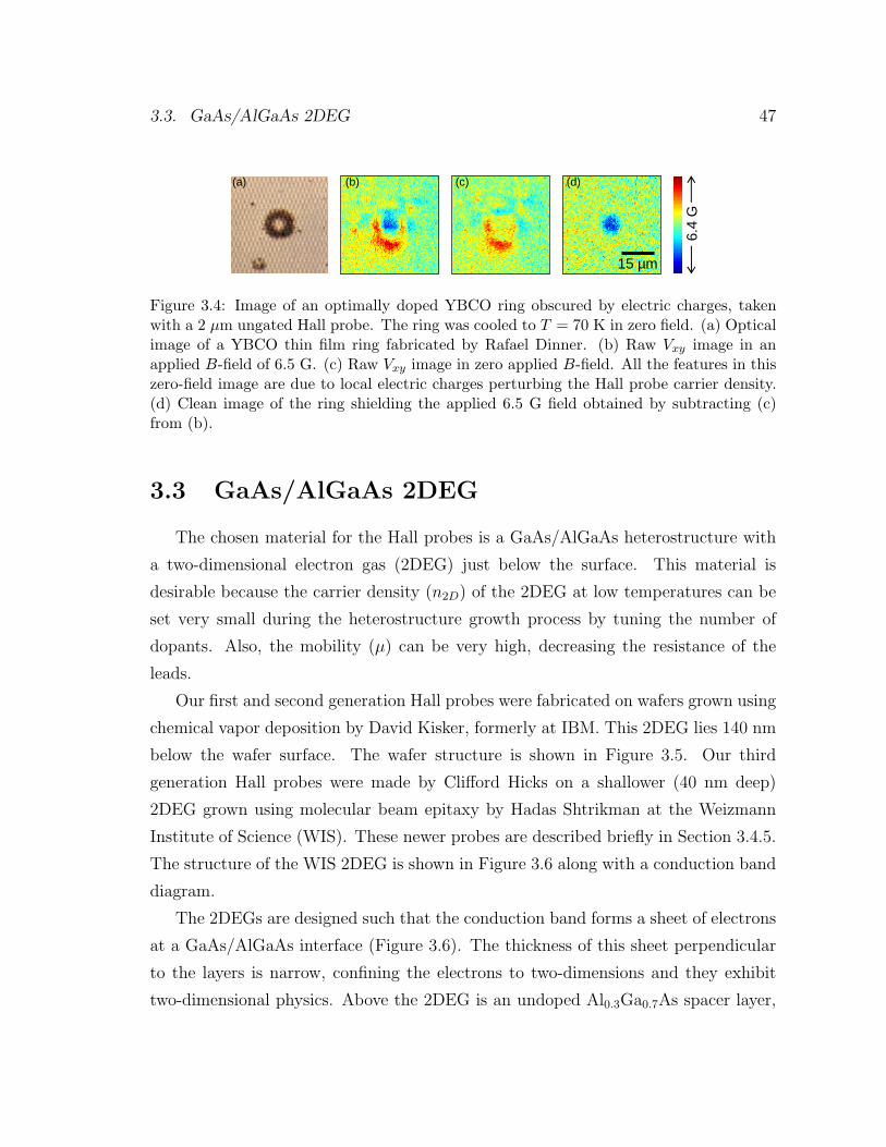
3.3. GaAs/AlGaAs 2DEG 47
6.4
G
(a) (b) (c) (d)
15 µm
Figure 3.4: Image of an optimally doped YBCO ring obscured by electric charges, takenwith a 2 µm ungated Hall probe. The ring was cooled to T = 70 K in zero field. (a) Opticalimage of a YBCO thin film ring fabricated by Rafael Dinner. (b) Raw Vxy image in anapplied B-field of 6.5 G. (c) Raw Vxy image in zero applied B-field. All the features in thiszero-field image are due to local electric charges perturbing the Hall probe carrier density.(d) Clean image of the ring shielding the applied 6.5 G field obtained by subtracting (c)from (b).
3.3 GaAs/AlGaAs 2DEG
The chosen material for the Hall probes is a GaAs/AlGaAs heterostructure with
a two-dimensional electron gas (2DEG) just below the surface. This material is
desirable because the carrier density (n2D) of the 2DEG at low temperatures can be
set very small during the heterostructure growth process by tuning the number of
dopants. Also, the mobility (µ) can be very high, decreasing the resistance of the
leads.
Our first and second generation Hall probes were fabricated on wafers grown using
chemical vapor deposition by David Kisker, formerly at IBM. This 2DEG lies 140 nm
below the wafer surface. The wafer structure is shown in Figure 3.5. Our third
generation Hall probes were made by Clifford Hicks on a shallower (40 nm deep)
2DEG grown using molecular beam epitaxy by Hadas Shtrikman at the Weizmann
Institute of Science (WIS). These newer probes are described briefly in Section 3.4.5.
The structure of the WIS 2DEG is shown in Figure 3.6 along with a conduction band
diagram.
The 2DEGs are designed such that the conduction band forms a sheet of electrons
at a GaAs/AlGaAs interface (Figure 3.6). The thickness of this sheet perpendicular
to the layers is narrow, confining the electrons to two-dimensions and they exhibit
two-dimensional physics. Above the 2DEG is an undoped Al0.3Ga0.7As spacer layer,
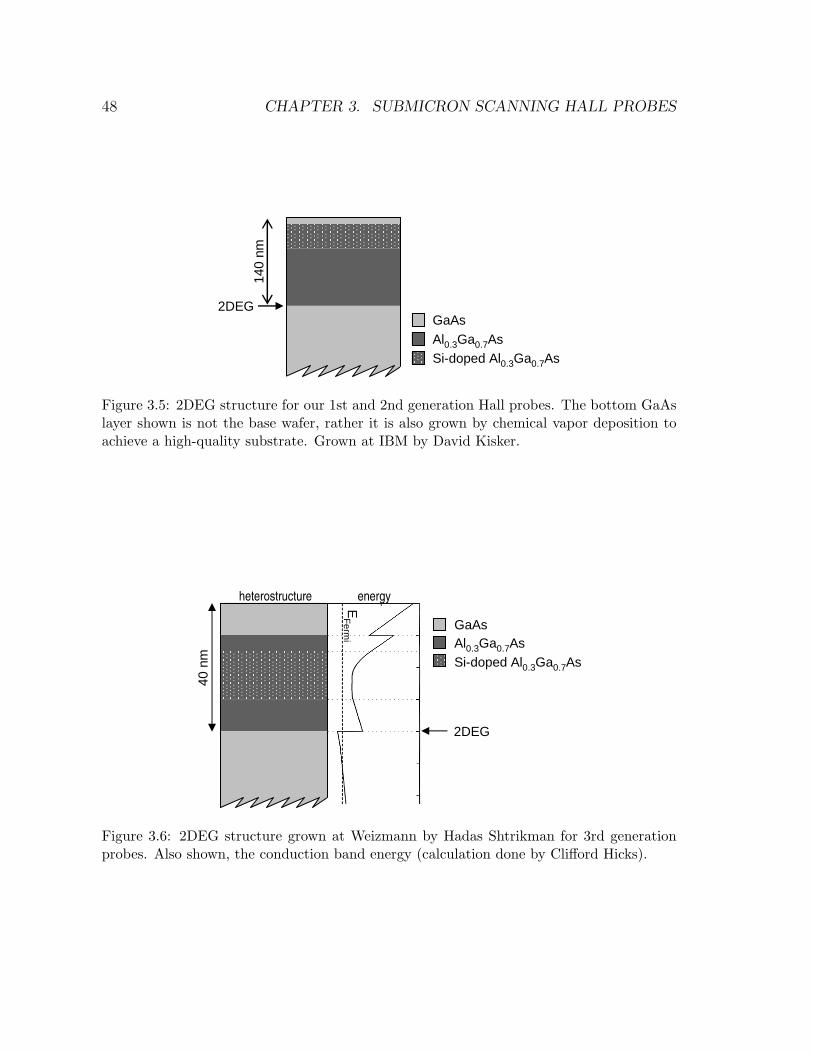
48 CHAPTER 3. SUBMICRON SCANNING HALL PROBES
GaAs
Al0.3Ga0.7AsSi-doped Al0.3Ga0.7As
140
nm
2DEG
Figure 3.5: 2DEG structure for our 1st and 2nd generation Hall probes. The bottom GaAslayer shown is not the base wafer, rather it is also grown by chemical vapor deposition toachieve a high-quality substrate. Grown at IBM by David Kisker.
40 n
m
2DEG
energyheterostructure
GaAsAl0.3Ga0.7AsSi-doped Al0.3Ga0.7As
EF
ermi
Figure 3.6: 2DEG structure grown at Weizmann by Hadas Shtrikman for 3rd generationprobes. Also shown, the conduction band energy (calculation done by Clifford Hicks).
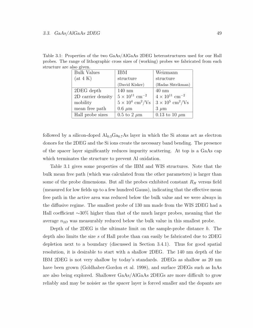
3.3. GaAs/AlGaAs 2DEG 49
Table 3.1: Properties of the two GaAs/AlGaAs 2DEG heterostructures used for our Hallprobes. The range of lithographic cross sizes of (working) probes we fabricated from eachstructure are also given.
Bulk Values IBM Weizmann(at 4 K) structure structure
(David Kisker) (Hadas Shtrikman)2DEG depth 140 nm 40 nm2D carrier density 5× 1011 cm−2 4× 1011 cm−2
mobility 5× 104 cm2/Vs 3× 105 cm2/Vsmean free path 0.6 µm 3 µmHall probe sizes 0.5 to 2 µm 0.13 to 10 µm
followed by a silicon-doped Al0.3Ga0.7As layer in which the Si atoms act as electron
donors for the 2DEG and the Si ions create the necessary band bending. The presence
of the spacer layer significantly reduces impurity scattering. At top is a GaAs cap
which terminates the structure to prevent Al oxidation.
Table 3.1 gives some properties of the IBM and WIS structures. Note that the
bulk mean free path (which was calculated from the other parameters) is larger than
some of the probe dimensions. But all the probes exhibited constant RH versus field
(measured for low fields up to a few hundred Gauss), indicating that the effective mean
free path in the active area was reduced below the bulk value and we were always in
the diffusive regime. The smallest probe of 130 nm made from the WIS 2DEG had a
Hall coefficient ∼30% higher than that of the much larger probes, meaning that the
average n2D was measurably reduced below the bulk value in this smallest probe.
Depth of the 2DEG is the ultimate limit on the sample-probe distance h. The
depth also limits the size s of Hall probe than can easily be fabricated due to 2DEG
depletion next to a boundary (discussed in Section 3.4.1). Thus for good spatial
resolution, it is desirable to start with a shallow 2DEG. The 140 nm depth of the
IBM 2DEG is not very shallow by today’s standards. 2DEGs as shallow as 20 nm
have been grown (Goldhaber-Gordon et al. 1998), and surface 2DEGs such as InAs
are also being explored. Shallower GaAs/AlGaAs 2DEGs are more difficult to grow
reliably and may be noisier as the spacer layer is forced smaller and the dopants are
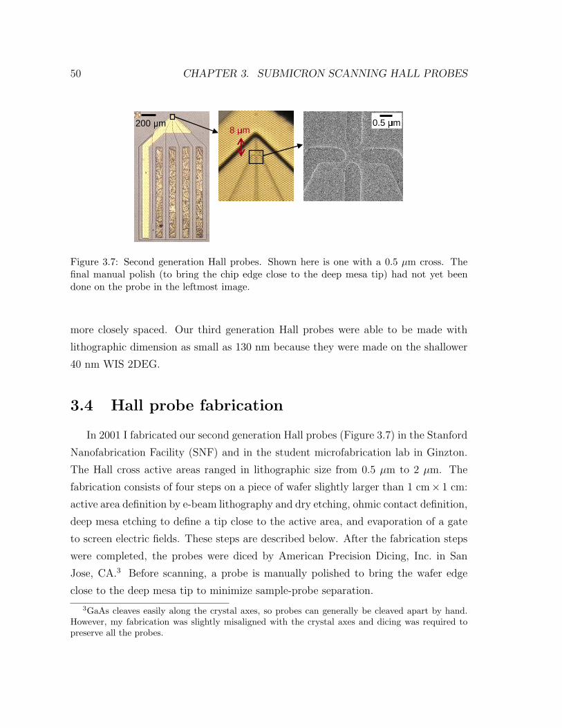
50 CHAPTER 3. SUBMICRON SCANNING HALL PROBES
200 m8 m
0.5 m
Figure 3.7: Second generation Hall probes. Shown here is one with a 0.5 µm cross. Thefinal manual polish (to bring the chip edge close to the deep mesa tip) had not yet beendone on the probe in the leftmost image.
more closely spaced. Our third generation Hall probes were able to be made with
lithographic dimension as small as 130 nm because they were made on the shallower
40 nm WIS 2DEG.
3.4 Hall probe fabrication
In 2001 I fabricated our second generation Hall probes (Figure 3.7) in the Stanford
Nanofabrication Facility (SNF) and in the student microfabrication lab in Ginzton.
The Hall cross active areas ranged in lithographic size from 0.5 µm to 2 µm. The
fabrication consists of four steps on a piece of wafer slightly larger than 1 cm× 1 cm:
active area definition by e-beam lithography and dry etching, ohmic contact definition,
deep mesa etching to define a tip close to the active area, and evaporation of a gate
to screen electric fields. These steps are described below. After the fabrication steps
were completed, the probes were diced by American Precision Dicing, Inc. in San
Jose, CA.3 Before scanning, a probe is manually polished to bring the wafer edge
close to the deep mesa tip to minimize sample-probe separation.
3GaAs cleaves easily along the crystal axes, so probes can generally be cleaved apart by hand.However, my fabrication was slightly misaligned with the crystal axes and dicing was required topreserve all the probes.
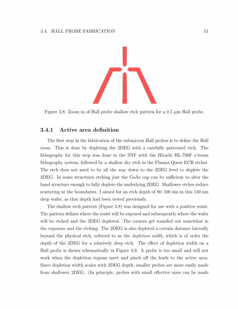
3.4. HALL PROBE FABRICATION 51
Figure 3.8: Zoom in of Hall probe shallow etch pattern for a 0.5 µm Hall probe.
3.4.1 Active area definition
The first step in the fabrication of the submicron Hall probes is to define the Hall
cross. This is done by depleting the 2DEG with a carefully patterned etch. The
lithography for this step was done in the SNF with the Hitachi HL-700F e-beam
lithography system, followed by a shallow dry etch in the Plasma Quest ECR etcher.
The etch does not need to be all the way down to the 2DEG level to deplete the
2DEG. In some structures etching just the GaAs cap can be sufficient to alter the
band structure enough to fully deplete the underlying 2DEG. Shallower etches reduce
scattering at the boundaries. I aimed for an etch depth of 80–100 nm in this 140 nm
deep wafer, as that depth had been tested previously.
The shallow etch pattern (Figure 3.8) was designed for use with a positive resist.
The pattern defines where the resist will be exposed and subsequently where the wafer
will be etched and the 2DEG depleted. The corners get rounded out somewhat in
the exposure and the etching. The 2DEG is also depleted a certain distance laterally
beyond the physical etch, referred to as the depletion width, which is of order the
depth of the 2DEG for a relatively deep etch. The effect of depletion width on a
Hall probe is shown schematically in Figure 3.9. A probe is too small and will not
work when the depletion regions meet and pinch off the leads to the active area.
Since depletion width scales with 2DEG depth, smaller probes are more easily made
from shallower 2DEG. (In principle, probes with small effective sizes can be made
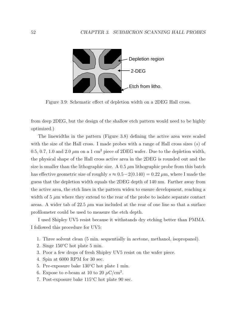
52 CHAPTER 3. SUBMICRON SCANNING HALL PROBES
Depletion region
2-DEG
Etch from litho.
Figure 3.9: Schematic effect of depletion width on a 2DEG Hall cross.
from deep 2DEG, but the design of the shallow etch pattern would need to be highly
optimized.)
The linewidths in the pattern (Figure 3.8) defining the active area were scaled
with the size of the Hall cross. I made probes with a range of Hall cross sizes (s) of
0.5, 0.7, 1.0 and 2.0 µm on a 1 cm2 piece of 2DEG wafer. Due to the depletion width,
the physical shape of the Hall cross active area in the 2DEG is rounded out and the
size is smaller than the lithographic size. A 0.5 µm lithographic probe from this batch
has effective geometric size of roughly s ≈ 0.5−2(0.140) = 0.22 µm, where I made the
guess that the depletion width equals the 2DEG depth of 140 nm. Farther away from
the active area, the etch lines in the pattern widen to ensure development, reaching a
width of 5 µm where they extend to the rear of the probe to isolate separate contact
areas. A wider tab of 22.5 µm was included at the rear of one line so that a surface
profilometer could be used to measure the etch depth.
I used Shipley UV5 resist because it withstands dry etching better than PMMA.
I followed this procedure for UV5:
1. Three solvent clean (5 min. sequentially in acetone, methanol, isopropanol).
2. Singe 150C hot plate 5 min.
3. Poor a few drops of fresh Shipley UV5 resist on the wafer piece.
4. Spin at 6000 RPM for 30 sec.
5. Pre-exposure bake 130C hot plate 1 min.
6. Expose to e-beam at 10 to 20 µC/cm2.
7. Post-exposure bake 115C hot plate 90 sec.
3.4. HALL PROBE FABRICATION 53
8. Develop in Shipley LDD-26W developer for 45 sec.
9. Hard bake at 145C hot plate 3 min.
It is important to bake and develop the resist just after the exposure. During the
e-beam run for these Hall probes I used 13–16 µC/cm2 for the largest to smallest Hall
cross sizes respectively. Lower exposures were used for the larger linewidths because
neighboring regions get partially exposed by the nearby beam due to the proximity
effect (Williams 1990, p. 143).
The next step in defining the active area was the etch process on the exposed
and developed wafer. First I did an oxygen plasma descum in the Plasma Asher in
Ginzton to remove any residual resist left behind in the exposed regions. It was not
clear if this was necessary, but it may have helped ensure homogeneous etching. Then
I ran the wafers in the SNF Plasma Quest. The process was 15 sccm Ar, 10 sccm
BCl3, and 3 sccm Cl2, with RF forward power at 35 and reflected power measuring
2.0. I etched for 40 sec. with sample temperature ∼23C which gave an average depth
of 85 nm. This process was chosen as a non-selective GaAs/AlGaAs etch.
3.4.2 Ohmic contacts
The next step in the Hall probe fabrication was to put ohmic contacts on the
probes which allow electrical connections to be made to the 2DEG. I used a Ni-Au-
Ge structure for the metal ohmics. It is believed that the during the anneal of the
contacts, Ga atoms diffuse out of the wafer and Ge atoms spike down into the wafer
creating electrical connection to the 2DEG. The Ni acts as a wetting layer and can
be successfully replaced with Pt (Lin and Lee 1990) in critical applications where no
magnetic material can be present.
The four ohmic contact pads per probe were 90 µm× 1500 µm and can be seen in
the left-most picture in Figure 3.7. Their mottled appearance indicates a successful
anneal. Optical lithography with a Karl Suss MA-6 Contact Mask Aligner was used
to define these large features. The ohmic fabrication process was as follows:
1. Three solvent clean.
2. Singe 150C hot plate 5 min.
54 CHAPTER 3. SUBMICRON SCANNING HALL PROBES
3. Poor a few drops of fresh Shipley 3612 photoresist on the piece.
4. Spin at 3500 RPM for 35 sec.
5. Pre-exposure bake 90C hot plate 1 min.
6. Remove resist at corners with a pointed Q-tip wet with acetone.
7. Expose on SNF Karl Suss for 1.2 sec. (at 15 mW/cm2).
8. Develop in Shipley LDD-26W developer for 90 sec.
9. O2 plasma descum in Ginzton 0.08 min. (Process 5).
10. HF dip just before evaporation, 15 sec. in 20:1 BOE.
11. Evaporate Ni-Au-Ge metal layers.
12. Lift-off in acetone.
The HF dip is done to strip off oxide so that the metal will stick. After the dip I
dunked the sample in DI water then blew it dry. Some oxide may reoccur during the
quick DI dip, but HF is highly toxic, so I felt it was best to rinse first then blow dry.
The metal was evaporated by Tom Carver with an e-beam evaporation system in this
order:
Ni 40 A
Ge 100 A
Au 100 A
Ge 60 A
Au 240 A
Ni 160 A
Au 2500 A
After liftoff the ohmics can be annealed. The anneal was done in the Rapid Thermal
Annealer (RTA) in Ginzton. The two parameters temperature and time can be chosen
for the anneal and to an extent, increases in either have a similar effect on the outcome.
For these Hall probes I had to anneal at a high temperature of 530C for 40 sec.
to get the mottled appearance indicative of a good anneal. This is a significantly
higher temperature than I used in earlier fabrications (475C for 30 sec.) and than
is used in the literature (e.g. Lin and Lee 1990). Tests by Yu-Ju Lin and my own
tests with dummy GaAs pieces in this RTA around the same time showed that lower
temperature readings were not sufficiently annealing the contacts. The RTA may have
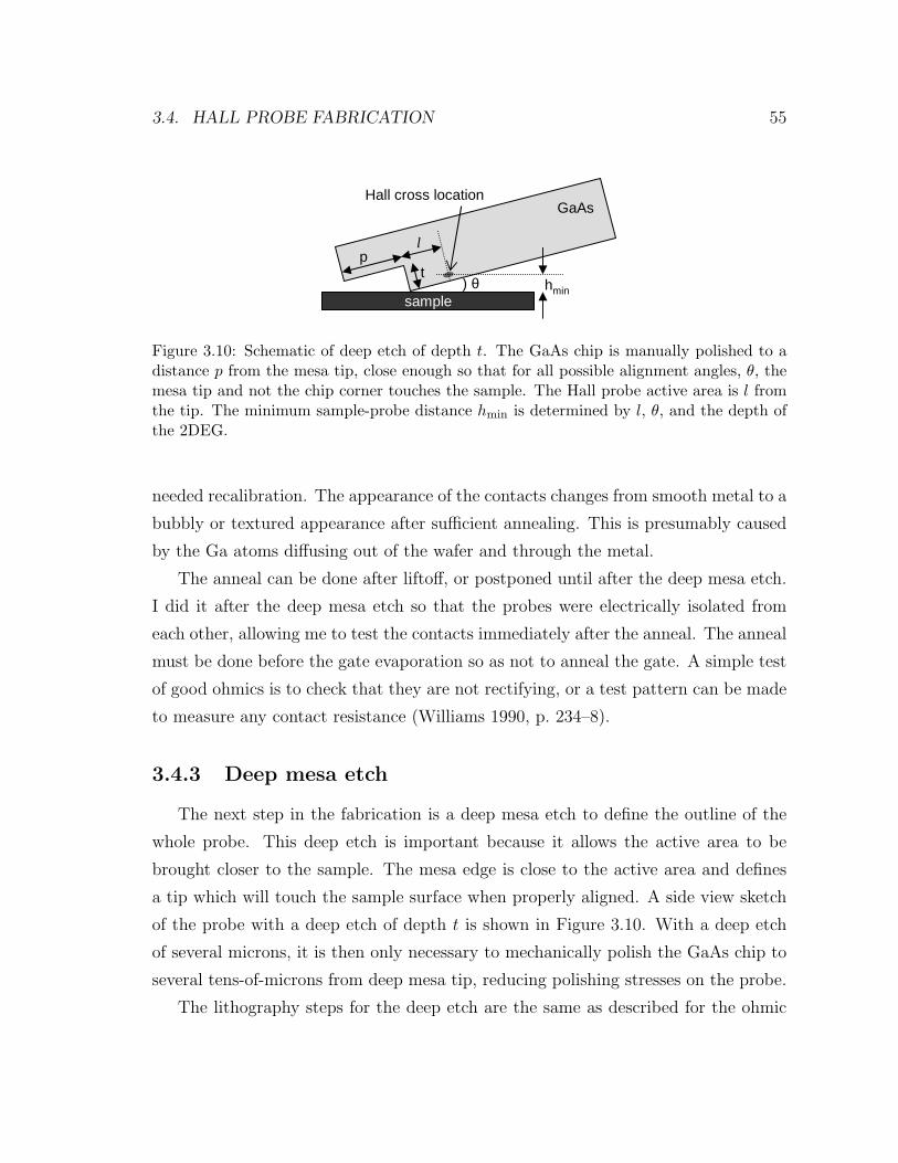
3.4. HALL PROBE FABRICATION 55
) θsample
GaAsHall cross location
pt
l
hmin
Figure 3.10: Schematic of deep etch of depth t. The GaAs chip is manually polished to adistance p from the mesa tip, close enough so that for all possible alignment angles, θ, themesa tip and not the chip corner touches the sample. The Hall probe active area is l fromthe tip. The minimum sample-probe distance hmin is determined by l, θ, and the depth ofthe 2DEG.
needed recalibration. The appearance of the contacts changes from smooth metal to a
bubbly or textured appearance after sufficient annealing. This is presumably caused
by the Ga atoms diffusing out of the wafer and through the metal.
The anneal can be done after liftoff, or postponed until after the deep mesa etch.
I did it after the deep mesa etch so that the probes were electrically isolated from
each other, allowing me to test the contacts immediately after the anneal. The anneal
must be done before the gate evaporation so as not to anneal the gate. A simple test
of good ohmics is to check that they are not rectifying, or a test pattern can be made
to measure any contact resistance (Williams 1990, p. 234–8).
3.4.3 Deep mesa etch
The next step in the fabrication is a deep mesa etch to define the outline of the
whole probe. This deep etch is important because it allows the active area to be
brought closer to the sample. The mesa edge is close to the active area and defines
a tip which will touch the sample surface when properly aligned. A side view sketch
of the probe with a deep etch of depth t is shown in Figure 3.10. With a deep etch
of several microns, it is then only necessary to mechanically polish the GaAs chip to
several tens-of-microns from deep mesa tip, reducing polishing stresses on the probe.
The lithography steps for the deep etch are the same as described for the ohmic
56 CHAPTER 3. SUBMICRON SCANNING HALL PROBES
contacts steps 1–8, followed by a 110C bake on the hot plate for 60 sec. after de-
veloping. The wet etch recipe is from DeSalvo et al. (1992) and is a 4:1:10 ratio by
volume of a citric acid mix, H2O2 (30% concentration), and water. The citric acid
mix is a 1:1 mix of anhydrous citric acid and water by weight, or in my case a 1.187:1
mix by weight of citric acid monohydrate and water. The solution’s 4:1:10 ratio was
chosen for its non-selectivity of GaAs and AlGaAs. Other ratios can be used for a
selective etch (DeSalvo et al. 1992). The etch rate is ∼0.14 µm/min. The solution
etches vertically and laterally at approximately the same rate, so it is important to
consider the lateral etching when aligning the deep etch pattern to the Hall probe
active area. The depth t should be at least 2 µm. From Figure 3.10 we see that
for the tip of the mesa to touch the sample surface, the depth of the etch must be
t > p tan θ. So to not have to polish the wafer closer than p = 30 µm, and to be safe
for all θ ≤ 3, we need t > 1.6 µm.
3.4.4 Screening gate
The final Hall probe fabrication step is to put a metal gate over the active area.
Its main purpose is to screen electric fields which can interfere with the magnetic
Hall signal, as described above in Section 3.2. The gate is intended to be grounded,
although it could also be held at a fixed voltage with respect to the Hall probe in
order to alter the carrier density. Possible side benefits of the gate may also be to
improve the mechanical robustness of the tip and for use as a scanning tunnelling
microscopy (STM) tip.
The gate was designed to overlay several hundred microns of the probe near the
tip and to extend out over the deep mesa edge by tens of microns. On the mask, the
gate extends out over the deep mesa edge by 20 µm. This distance was chosen to
be close enough that the metal would not be polished when manually polishing the
probe for scanning, but far enough away to make sure the tip was covered (for STM
use if desired) and that any edge wall from the metal evaporation would remain in
the deep etched region. The gate can be seen in Figure 3.7.
Gold was chosen for the gate metal, since it is non-magnetic and easy to wire
3.4. HALL PROBE FABRICATION 57
bond. First, a thin titanium layer was evaporated as a wetting layer to help the gold
stick. Tom Carver recommended 5–25 nm for the wetting layer thickness. For the
overall thickness, it is desirable to have as thin a gate as possible so as not to add
significantly to the minimum scanning height of the Hall probe. However, the gate
needs to be thicker than the shallow etch depth (80–100 nm) to ensure continuity.
Shipley Megaposit SPR220-7 positive photoresist was used since it is necessary
to entirely cover the probes after the deep mesa etch. I altered the SNF process for
7 µm resist by increasing the spin speed to 6500 RPM, giving 5.2 µm thickness. The
metal gate process is as follows:
1. Three solvent clean.
2. Singe 150C hot plate 5 min.
3. Poor a few drops of fresh Shipley SPR220-7 photoresist on the piece.
4. Spin at 6500 RPM for 45 sec. (accel. 2000 on Laurel spinner).
5. Bake 90C hot plate for 200 sec.
6. Remove resist at corners with a pointed Q-tip wet with acetone.
7. Over-expose 11.5± 3 sec. on SNF Karl Suss (at 15 mW/cm2).
8. Develop in Shipley LDD-26W developer for 1–2 min.
9. O2 plasma descum in Ginzton 0.08 min. (Process 5).
10. HF dip just before evaporation, 15 sec. in 20:1 BOE.
11. Evaporate 125 A titanium followed by 1250 A gold.
12. Lift-off in acetone.
Tom Carver did the HF dip and evaporation.
For future Hall probe processing, it may make sense to sacrifice the STM ability
(which I have never used) by not bringing the gate over the edge of the tip. Then
the gate process can be done before the deep etch using a much thinner resist. It is
advantageous to have the gate cover only a very small area of the 2DEG around the
Hall cross to reduce coupling between the gate and 2DEG, but I did not realize that
when I designed my mask.
A concern for gates on shallow 2DEG is leakage between the 2DEG and the gate.
For Hall probes made on the 140 nm deep 2DEG, this is not an issue at 4 K. I applied
a voltage between the gate and one Hall probe ohmic contact. See Figure 3.11. For
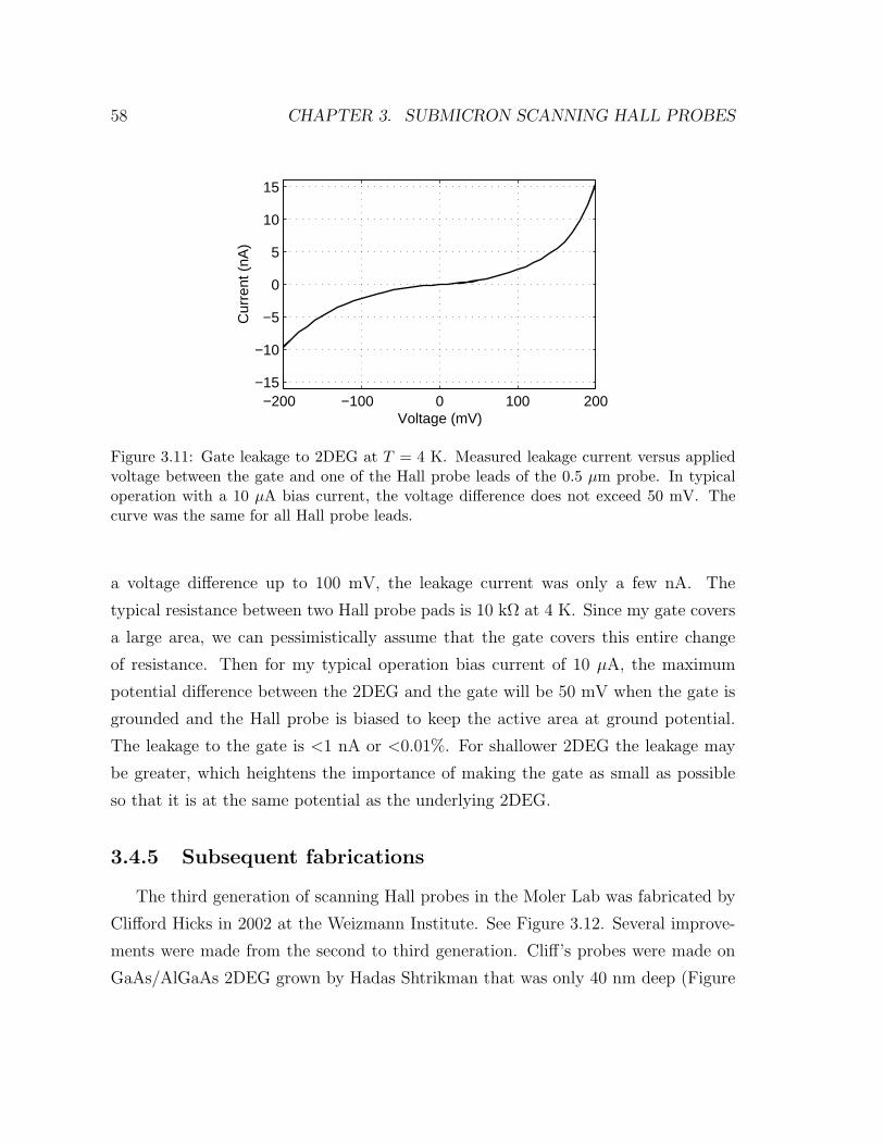
58 CHAPTER 3. SUBMICRON SCANNING HALL PROBES
−200 −100 0 100 200−15
−10
−5
0
5
10
15
Voltage (mV)
Cur
rent
(nA
)
Figure 3.11: Gate leakage to 2DEG at T = 4 K. Measured leakage current versus appliedvoltage between the gate and one of the Hall probe leads of the 0.5 µm probe. In typicaloperation with a 10 µA bias current, the voltage difference does not exceed 50 mV. Thecurve was the same for all Hall probe leads.
a voltage difference up to 100 mV, the leakage current was only a few nA. The
typical resistance between two Hall probe pads is 10 kΩ at 4 K. Since my gate covers
a large area, we can pessimistically assume that the gate covers this entire change
of resistance. Then for my typical operation bias current of 10 µA, the maximum
potential difference between the 2DEG and the gate will be 50 mV when the gate is
grounded and the Hall probe is biased to keep the active area at ground potential.
The leakage to the gate is <1 nA or <0.01%. For shallower 2DEG the leakage may
be greater, which heightens the importance of making the gate as small as possible
so that it is at the same potential as the underlying 2DEG.
3.4.5 Subsequent fabrications
The third generation of scanning Hall probes in the Moler Lab was fabricated by
Clifford Hicks in 2002 at the Weizmann Institute. See Figure 3.12. Several improve-
ments were made from the second to third generation. Cliff’s probes were made on
GaAs/AlGaAs 2DEG grown by Hadas Shtrikman that was only 40 nm deep (Figure
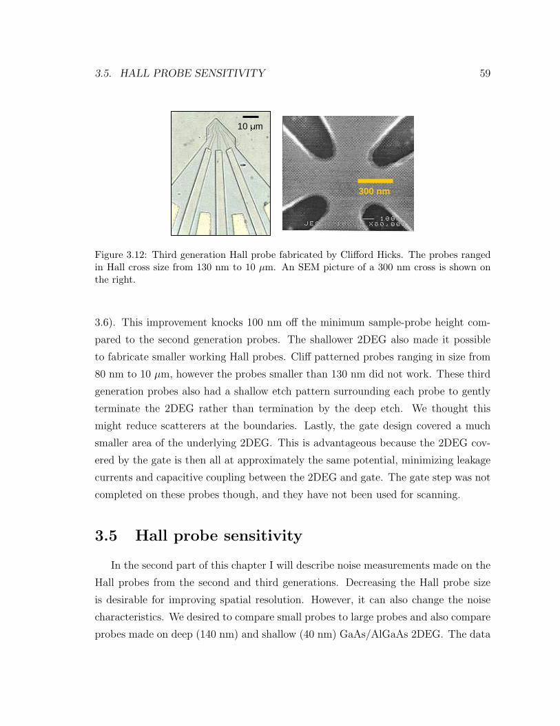
3.5. HALL PROBE SENSITIVITY 59
300 nm
10 m
Figure 3.12: Third generation Hall probe fabricated by Clifford Hicks. The probes rangedin Hall cross size from 130 nm to 10 µm. An SEM picture of a 300 nm cross is shown onthe right.
3.6). This improvement knocks 100 nm off the minimum sample-probe height com-
pared to the second generation probes. The shallower 2DEG also made it possible
to fabricate smaller working Hall probes. Cliff patterned probes ranging in size from
80 nm to 10 µm, however the probes smaller than 130 nm did not work. These third
generation probes also had a shallow etch pattern surrounding each probe to gently
terminate the 2DEG rather than termination by the deep etch. We thought this
might reduce scatterers at the boundaries. Lastly, the gate design covered a much
smaller area of the underlying 2DEG. This is advantageous because the 2DEG cov-
ered by the gate is then all at approximately the same potential, minimizing leakage
currents and capacitive coupling between the 2DEG and gate. The gate step was not
completed on these probes though, and they have not been used for scanning.
3.5 Hall probe sensitivity
In the second part of this chapter I will describe noise measurements made on the
Hall probes from the second and third generations. Decreasing the Hall probe size
is desirable for improving spatial resolution. However, it can also change the noise
characteristics. We desired to compare small probes to large probes and also compare
probes made on deep (140 nm) and shallow (40 nm) GaAs/AlGaAs 2DEG. The data
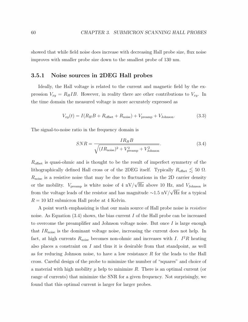
60 CHAPTER 3. SUBMICRON SCANNING HALL PROBES
showed that while field noise does increase with decreasing Hall probe size, flux noise
improves with smaller probe size down to the smallest probe of 130 nm.
3.5.1 Noise sources in 2DEG Hall probes
Ideally, the Hall voltage is related to the current and magnetic field by the ex-
pression Vxy = RHIB. However, in reality there are other contributions to Vxy. In
the time domain the measured voltage is more accurately expressed as
Vxy(t) = I(RHB + Roffset + Rnoise) + Vpreamp + VJohnson. (3.3)
The signal-to-noise ratio in the frequency domain is
SNR =IRHB√
(IRnoise)2 + V 2preamp + V 2
Johnson
. (3.4)
Roffset is quasi-ohmic and is thought to be the result of imperfect symmetry of the
lithographically defined Hall cross or of the 2DEG itself. Typically Roffset . 50 Ω.
Rnoise is a resistive noise that may be due to fluctuations in the 2D carrier density
or the mobility. Vpreamp is white noise of 4 nV/√
Hz above 10 Hz, and VJohnson is
from the voltage leads of the resistor and has magnitude ∼1.5 nV/√
Hz for a typical
R = 10 kΩ submicron Hall probe at 4 Kelvin.
A point worth emphasizing is that our main source of Hall probe noise is resistive
noise. As Equation (3.4) shows, the bias current I of the Hall probe can be increased
to overcome the preamplifier and Johnson voltage noise. But once I is large enough
that IRnoise is the dominant voltage noise, increasing the current does not help. In
fact, at high currents Rnoise becomes non-ohmic and increases with I. I2R heating
also places a constraint on I and thus it is desirable from that standpoint, as well
as for reducing Johnson noise, to have a low resistance R for the leads to the Hall
cross. Careful design of the probe to minimize the number of “squares” and choice of
a material with high mobility µ help to minimize R. There is an optimal current (or
range of currents) that minimize the SNR for a given frequency. Not surprisingly, we
found that this optimal current is larger for larger probes.
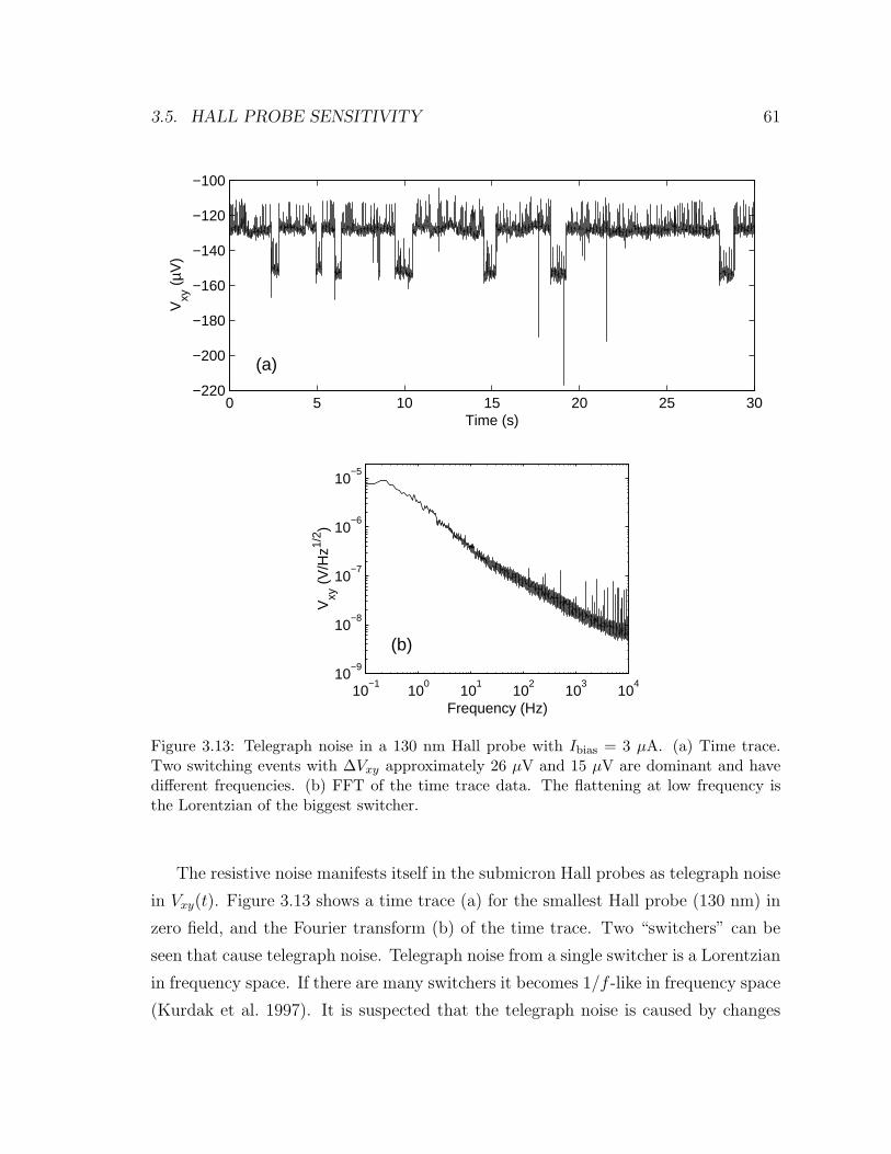
3.5. HALL PROBE SENSITIVITY 61
0 5 10 15 20 25 30−220
−200
−180
−160
−140
−120
−100
Time (s)
Vxy
(µV
)
(a)
10−1
100
101
102
103
104
10−9
10−8
10−7
10−6
10−5
Frequency (Hz)
Vxy
(V
/Hz1/
2 )
(b)
Figure 3.13: Telegraph noise in a 130 nm Hall probe with Ibias = 3 µA. (a) Time trace.Two switching events with ∆Vxy approximately 26 µV and 15 µV are dominant and havedifferent frequencies. (b) FFT of the time trace data. The flattening at low frequency isthe Lorentzian of the biggest switcher.
The resistive noise manifests itself in the submicron Hall probes as telegraph noise
in Vxy(t). Figure 3.13 shows a time trace (a) for the smallest Hall probe (130 nm) in
zero field, and the Fourier transform (b) of the time trace. Two “switchers” can be
seen that cause telegraph noise. Telegraph noise from a single switcher is a Lorentzian
in frequency space. If there are many switchers it becomes 1/f -like in frequency space
(Kurdak et al. 1997). It is suspected that the telegraph noise is caused by changes
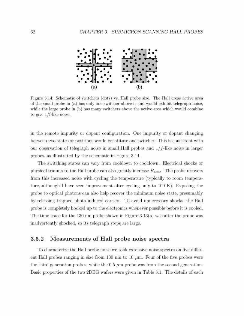
62 CHAPTER 3. SUBMICRON SCANNING HALL PROBES
(a) (b)
Figure 3.14: Schematic of switchers (dots) vs. Hall probe size. The Hall cross active areaof the small probe in (a) has only one switcher above it and would exhibit telegraph noise,while the large probe in (b) has many switchers above the active area which would combineto give 1/f-like noise.
in the remote impurity or dopant configuration. One impurity or dopant changing
between two states or positions would constitute one switcher. This is consistent with
our observation of telegraph noise in small Hall probes and 1/f -like noise in larger
probes, as illustrated by the schematic in Figure 3.14.
The switching states can vary from cooldown to cooldown. Electrical shocks or
physical trauma to the Hall probe can also greatly increase Rnoise. The probe recovers
from this increased noise with cycling the temperature (typically to room tempera-
ture, although I have seen improvement after cycling only to 100 K). Exposing the
probe to optical photons can also help recover the minimum noise state, presumably
by releasing trapped photo-induced carriers. To avoid unnecessary shocks, the Hall
probe is completely hooked up to the electronics whenever possible before it is cooled.
The time trace for the 130 nm probe shown in Figure 3.13(a) was after the probe was
inadvertently shocked, so its telegraph steps are large.
3.5.2 Measurements of Hall probe noise spectra
To characterize the Hall probe noise we took extensive noise spectra on five differ-
ent Hall probes ranging in size from 130 nm to 10 µm. Four of the five probes were
the third generation probes, while the 0.5 µm probe was from the second generation.
Basic properties of the two 2DEG wafers were given in Table 3.1. The details of each
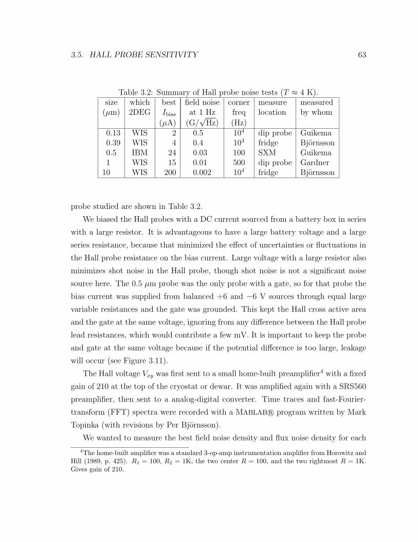
3.5. HALL PROBE SENSITIVITY 63
Table 3.2: Summary of Hall probe noise tests (T ≈ 4 K).size which best field noise corner measure measured(µm) 2DEG Ibias at 1 Hz freq location by whom
(µA) (G/√
Hz) (Hz)0.13 WIS 2 0.5 104 dip probe Guikema0.39 WIS 4 0.4 103 fridge Bjornsson0.5 IBM 24 0.03 100 SXM Guikema1 WIS 15 0.01 500 dip probe Gardner
10 WIS 200 0.002 104 fridge Bjornsson
probe studied are shown in Table 3.2.
We biased the Hall probes with a DC current sourced from a battery box in series
with a large resistor. It is advantageous to have a large battery voltage and a large
series resistance, because that minimized the effect of uncertainties or fluctuations in
the Hall probe resistance on the bias current. Large voltage with a large resistor also
minimizes shot noise in the Hall probe, though shot noise is not a significant noise
source here. The 0.5 µm probe was the only probe with a gate, so for that probe the
bias current was supplied from balanced +6 and −6 V sources through equal large
variable resistances and the gate was grounded. This kept the Hall cross active area
and the gate at the same voltage, ignoring from any difference between the Hall probe
lead resistances, which would contribute a few mV. It is important to keep the probe
and gate at the same voltage because if the potential difference is too large, leakage
will occur (see Figure 3.11).
The Hall voltage Vxy was first sent to a small home-built preamplifier4 with a fixed
gain of 210 at the top of the cryostat or dewar. It was amplified again with a SRS560
preamplifier, then sent to a analog-digital converter. Time traces and fast-Fourier-
transform (FFT) spectra were recorded with a MABLAB r© program written by Mark
Topinka (with revisions by Per Bjornsson).
We wanted to measure the best field noise density and flux noise density for each
4The home-built amplifier was a standard 3-op-amp instrumentation amplifier from Horowitz andHill (1989, p. 425). R1 = 100, R2 = 1K, the two center R = 100, and the two rightmost R = 1K.Gives gain of 210.
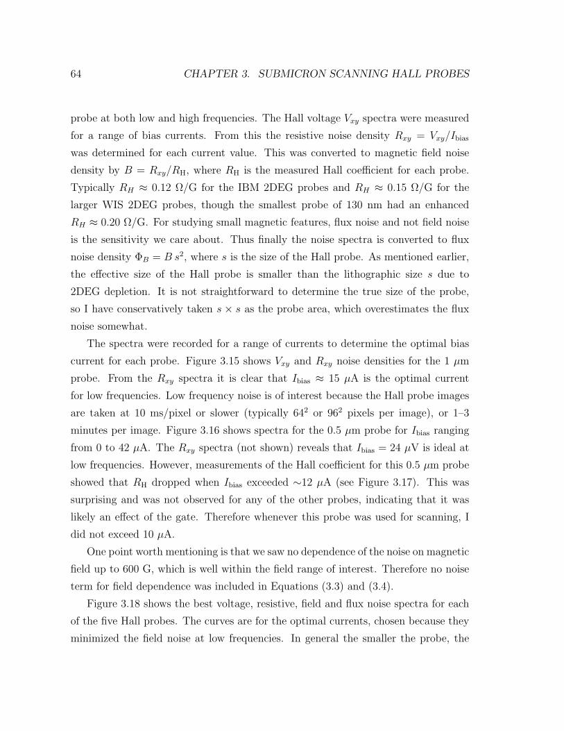
64 CHAPTER 3. SUBMICRON SCANNING HALL PROBES
probe at both low and high frequencies. The Hall voltage Vxy spectra were measured
for a range of bias currents. From this the resistive noise density Rxy = Vxy/Ibias
was determined for each current value. This was converted to magnetic field noise
density by B = Rxy/RH, where RH is the measured Hall coefficient for each probe.
Typically RH ≈ 0.12 Ω/G for the IBM 2DEG probes and RH ≈ 0.15 Ω/G for the
larger WIS 2DEG probes, though the smallest probe of 130 nm had an enhanced
RH ≈ 0.20 Ω/G. For studying small magnetic features, flux noise and not field noise
is the sensitivity we care about. Thus finally the noise spectra is converted to flux
noise density ΦB = B s2, where s is the size of the Hall probe. As mentioned earlier,
the effective size of the Hall probe is smaller than the lithographic size s due to
2DEG depletion. It is not straightforward to determine the true size of the probe,
so I have conservatively taken s × s as the probe area, which overestimates the flux
noise somewhat.
The spectra were recorded for a range of currents to determine the optimal bias
current for each probe. Figure 3.15 shows Vxy and Rxy noise densities for the 1 µm
probe. From the Rxy spectra it is clear that Ibias ≈ 15 µA is the optimal current
for low frequencies. Low frequency noise is of interest because the Hall probe images
are taken at 10 ms/pixel or slower (typically 642 or 962 pixels per image), or 1–3
minutes per image. Figure 3.16 shows spectra for the 0.5 µm probe for Ibias ranging
from 0 to 42 µA. The Rxy spectra (not shown) reveals that Ibias = 24 µV is ideal at
low frequencies. However, measurements of the Hall coefficient for this 0.5 µm probe
showed that RH dropped when Ibias exceeded ∼12 µA (see Figure 3.17). This was
surprising and was not observed for any of the other probes, indicating that it was
likely an effect of the gate. Therefore whenever this probe was used for scanning, I
did not exceed 10 µA.
One point worth mentioning is that we saw no dependence of the noise on magnetic
field up to 600 G, which is well within the field range of interest. Therefore no noise
term for field dependence was included in Equations (3.3) and (3.4).
Figure 3.18 shows the best voltage, resistive, field and flux noise spectra for each
of the five Hall probes. The curves are for the optimal currents, chosen because they
minimized the field noise at low frequencies. In general the smaller the probe, the
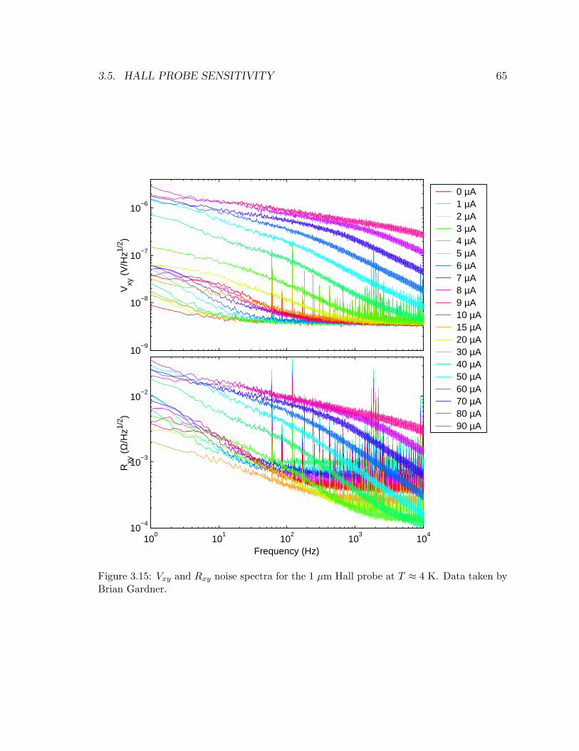
3.5. HALL PROBE SENSITIVITY 65
10−9
10−8
10−7
10−6
Vxy
(V
/Hz1/
2 )
0 µA1 µA2 µA3 µA4 µA5 µA6 µA7 µA8 µA9 µA10 µA15 µA20 µA30 µA40 µA50 µA60 µA70 µA80 µA90 µA
100
101
102
103
104
10−4
10−3
10−2
Frequency (Hz)
Rxy
(Ω
/Hz1/
2 )
Figure 3.15: Vxy and Rxy noise spectra for the 1 µm Hall probe at T ≈ 4 K. Data taken byBrian Gardner.
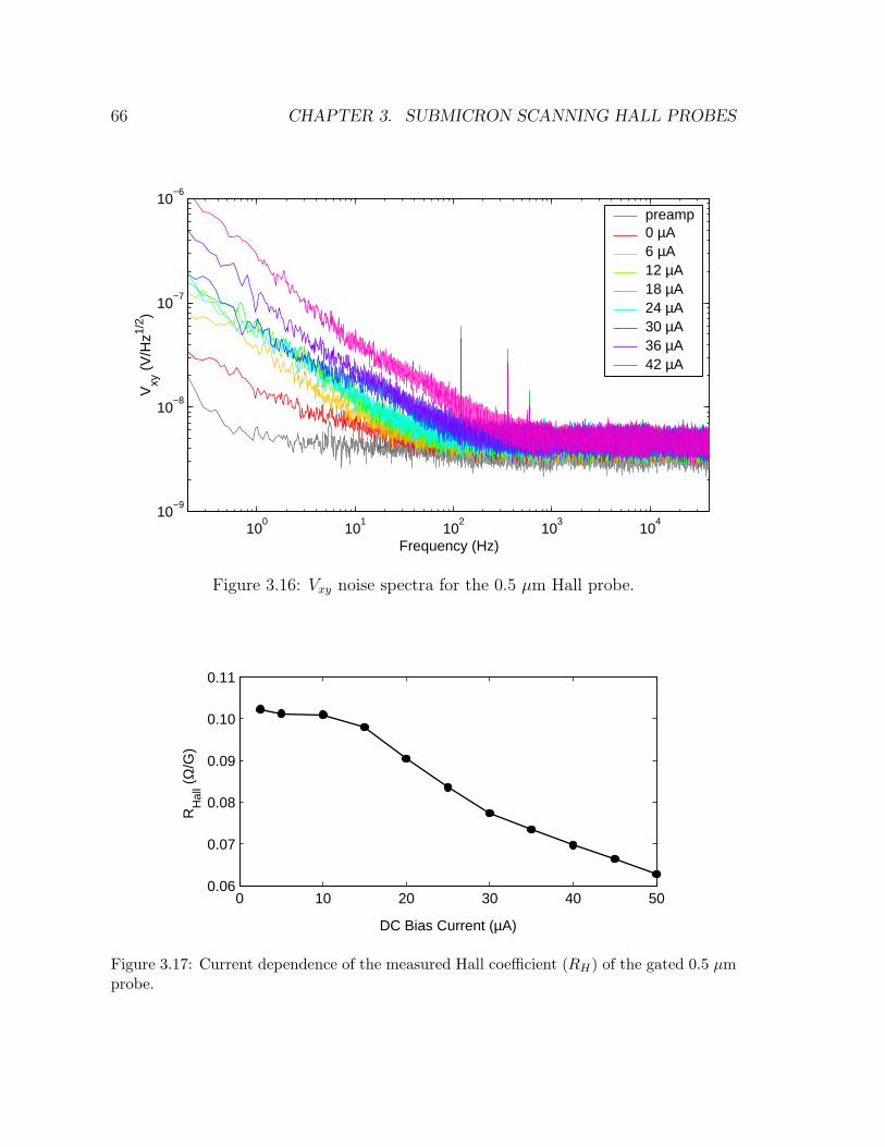
66 CHAPTER 3. SUBMICRON SCANNING HALL PROBES
100
101
102
103
104
10−9
10−8
10−7
10−6
Frequency (Hz)
Vxy
(V
/Hz1/
2 )
preamp0 µA6 µA12 µA18 µA24 µA30 µA36 µA42 µA
Figure 3.16: Vxy noise spectra for the 0.5 µm Hall probe.
0 10 20 30 40 500.06
0.07
0.08
0.09
0.10
0.11
RH
all (
Ω/G
)
DC Bias Current (µA)
Figure 3.17: Current dependence of the measured Hall coefficient (RH) of the gated 0.5 µmprobe.
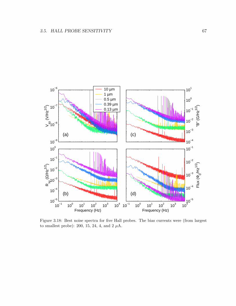
3.5. HALL PROBE SENSITIVITY 67
10−9
10−8
10−7
10−6
Vxy
(V
/Hz1/
2 )
(a)
10−1
100
101
102
103
104
10−5
10−4
10−3
10−2
10−1
100
Frequency (Hz)
Rxy
(Ω
/Hz1/
2 )
(b)
10−4
10−3
10−2
10−1
100
101
"B"
(G/H
z1/2 )
(c)
10−1
100
101
102
103
10410
−5
10−4
10−3
10−2
10−1
Flu
x (Φ
0/Hz1/
2 )
Frequency (Hz)
(d)
10 µm1 µm0.5 µm0.39 µm0.13 µm
Figure 3.18: Best noise spectra for five Hall probes. The bias currents were (from largestto smallest probe): 200, 15, 24, 4, and 2 µA.
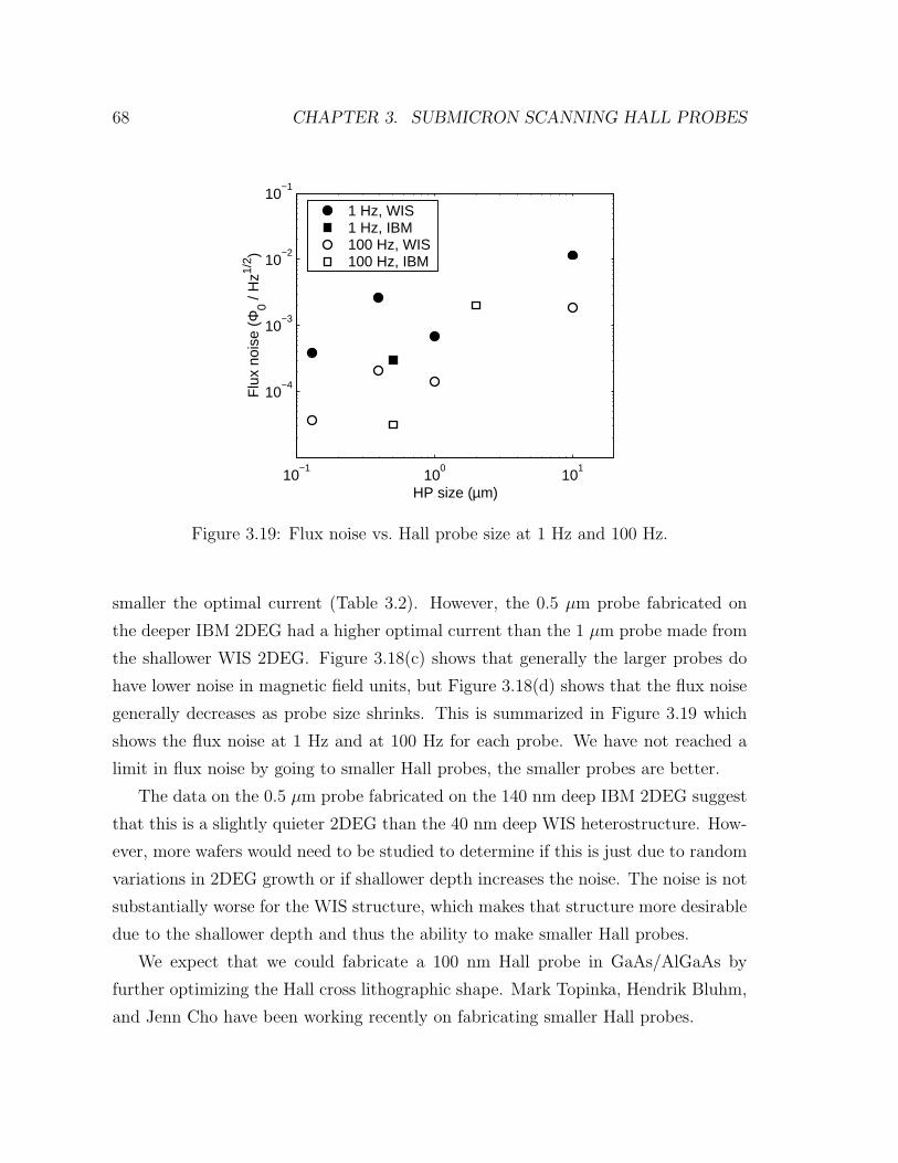
68 CHAPTER 3. SUBMICRON SCANNING HALL PROBES
10−1
100
101
10−4
10−3
10−2
10−1
HP size (µm)
Flu
x no
ise
(Φ0 /
Hz1/
2 )
1 Hz, WIS1 Hz, IBM100 Hz, WIS100 Hz, IBM
Figure 3.19: Flux noise vs. Hall probe size at 1 Hz and 100 Hz.
smaller the optimal current (Table 3.2). However, the 0.5 µm probe fabricated on
the deeper IBM 2DEG had a higher optimal current than the 1 µm probe made from
the shallower WIS 2DEG. Figure 3.18(c) shows that generally the larger probes do
have lower noise in magnetic field units, but Figure 3.18(d) shows that the flux noise
generally decreases as probe size shrinks. This is summarized in Figure 3.19 which
shows the flux noise at 1 Hz and at 100 Hz for each probe. We have not reached a
limit in flux noise by going to smaller Hall probes, the smaller probes are better.
The data on the 0.5 µm probe fabricated on the 140 nm deep IBM 2DEG suggest
that this is a slightly quieter 2DEG than the 40 nm deep WIS heterostructure. How-
ever, more wafers would need to be studied to determine if this is just due to random
variations in 2DEG growth or if shallower depth increases the noise. The noise is not
substantially worse for the WIS structure, which makes that structure more desirable
due to the shallower depth and thus the ability to make smaller Hall probes.
We expect that we could fabricate a 100 nm Hall probe in GaAs/AlGaAs by
further optimizing the Hall cross lithographic shape. Mark Topinka, Hendrik Bluhm,
and Jenn Cho have been working recently on fabricating smaller Hall probes.
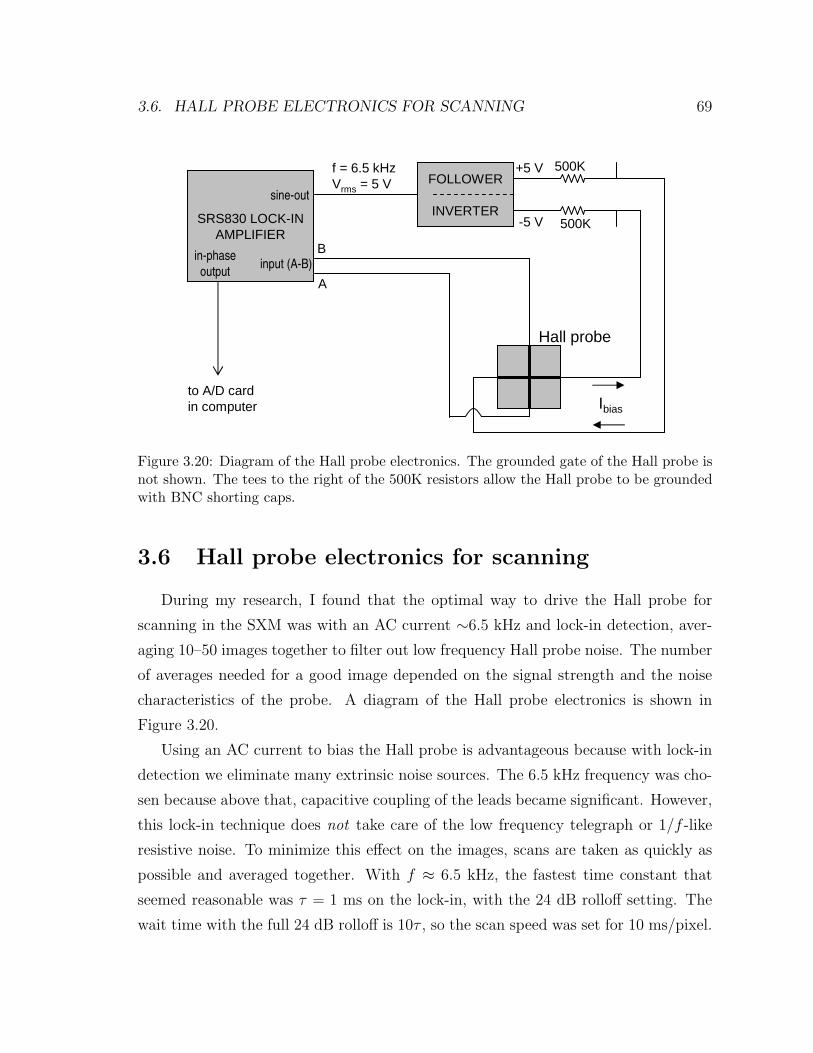
3.6. HALL PROBE ELECTRONICS FOR SCANNING 69
SRS830 LOCK-INAMPLIFIER
FOLLOWER
INVERTER
f = 6.5 kHzVrms = 5 V
+5 V
-5 V 500K
500K
Ibias
B
A
input (A-B)
sine-out
in-phase
output
to A/D cardin computer
Hall probe
Figure 3.20: Diagram of the Hall probe electronics. The grounded gate of the Hall probe isnot shown. The tees to the right of the 500K resistors allow the Hall probe to be groundedwith BNC shorting caps.
3.6 Hall probe electronics for scanning
During my research, I found that the optimal way to drive the Hall probe for
scanning in the SXM was with an AC current ∼6.5 kHz and lock-in detection, aver-
aging 10–50 images together to filter out low frequency Hall probe noise. The number
of averages needed for a good image depended on the signal strength and the noise
characteristics of the probe. A diagram of the Hall probe electronics is shown in
Figure 3.20.
Using an AC current to bias the Hall probe is advantageous because with lock-in
detection we eliminate many extrinsic noise sources. The 6.5 kHz frequency was cho-
sen because above that, capacitive coupling of the leads became significant. However,
this lock-in technique does not take care of the low frequency telegraph or 1/f -like
resistive noise. To minimize this effect on the images, scans are taken as quickly as
possible and averaged together. With f ≈ 6.5 kHz, the fastest time constant that
seemed reasonable was τ = 1 ms on the lock-in, with the 24 dB rolloff setting. The
wait time with the full 24 dB rolloff is 10τ , so the scan speed was set for 10 ms/pixel.
70 CHAPTER 3. SUBMICRON SCANNING HALL PROBES
Images can be acquired faster than this for diagnostic purposes or locating features
of interest. The lowest resonant frequencies of the S-bender scanner are ∼40 Hz, so
this scan speed of <2 Hz per line is certainly safe.
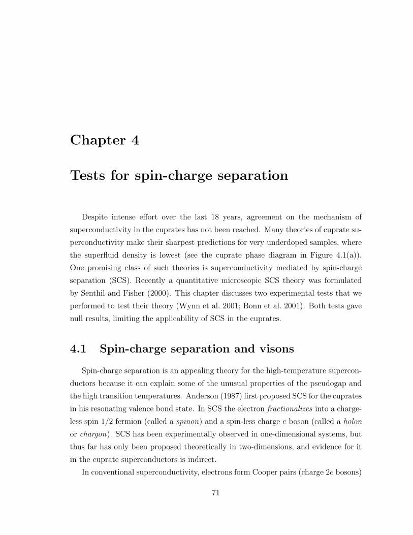
Chapter 4
Tests for spin-charge separation
Despite intense effort over the last 18 years, agreement on the mechanism of
superconductivity in the cuprates has not been reached. Many theories of cuprate su-
perconductivity make their sharpest predictions for very underdoped samples, where
the superfluid density is lowest (see the cuprate phase diagram in Figure 4.1(a)).
One promising class of such theories is superconductivity mediated by spin-charge
separation (SCS). Recently a quantitative microscopic SCS theory was formulated
by Senthil and Fisher (2000). This chapter discusses two experimental tests that we
performed to test their theory (Wynn et al. 2001; Bonn et al. 2001). Both tests gave
null results, limiting the applicability of SCS in the cuprates.
4.1 Spin-charge separation and visons
Spin-charge separation is an appealing theory for the high-temperature supercon-
ductors because it can explain some of the unusual properties of the pseudogap and
the high transition temperatures. Anderson (1987) first proposed SCS for the cuprates
in his resonating valence bond state. In SCS the electron fractionalizes into a charge-
less spin 1/2 fermion (called a spinon) and a spin-less charge e boson (called a holon
or chargon). SCS has been experimentally observed in one-dimensional systems, but
thus far has only been proposed theoretically in two-dimensions, and evidence for it
in the cuprate superconductors is indirect.
In conventional superconductivity, electrons form Cooper pairs (charge 2e bosons)
71
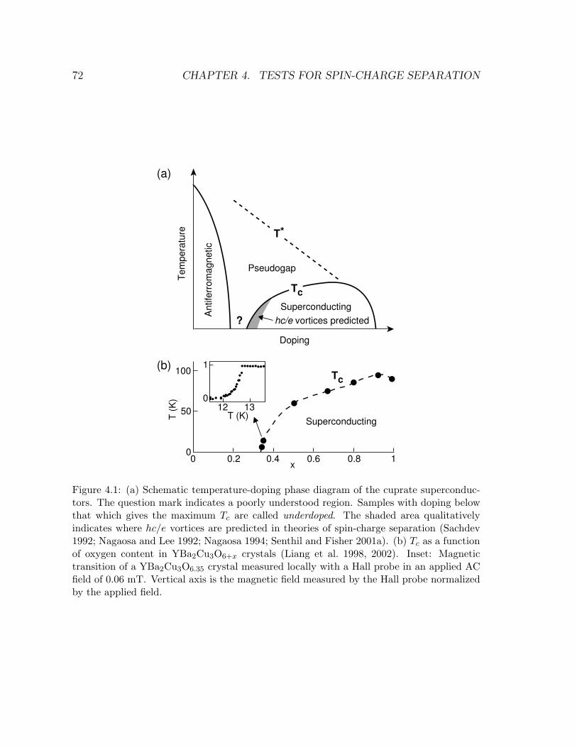
72 CHAPTER 4. TESTS FOR SPIN-CHARGE SEPARATION
Tc
x
T (
K)
100
Superconducting
0 0.2 0.4 0.6 0.8 10
50
(b)
Superconducting
Antife
rrom
agnetic
Pseudogap
Doping
Tem
pera
ture
(a)
hc/e vortices predicted
Tc
T*
?
T (K)12 13
0
1
Figure 4.1: (a) Schematic temperature-doping phase diagram of the cuprate superconduc-tors. The question mark indicates a poorly understood region. Samples with doping belowthat which gives the maximum Tc are called underdoped. The shaded area qualitativelyindicates where hc/e vortices are predicted in theories of spin-charge separation (Sachdev1992; Nagaosa and Lee 1992; Nagaosa 1994; Senthil and Fisher 2001a). (b) Tc as a functionof oxygen content in YBa2Cu3O6+x crystals (Liang et al. 1998, 2002). Inset: Magnetictransition of a YBa2Cu3O6.35 crystal measured locally with a Hall probe in an applied ACfield of 0.06 mT. Vertical axis is the magnetic field measured by the Hall probe normalizedby the applied field.
4.1. SPIN-CHARGE SEPARATION AND VISONS 73
which condense to the superconducting state. In SCS superconductivity, the chargons
could directly Bose condense without the need for pairing. Naively, hc/e flux quan-
tization would be expected from SCS superconductivity, because a charge e particle
circling an hc/e vortex acquires a 2π phase shift. This would be in contrast to the
conventional hc/2e superconducting flux quantum, which have also been observed in
cuprates (Gough et al. 1987). (See Sections 1.2.1 and 6.1 for details on fluxoid quan-
tization.) SCS theories do in fact allow hc/2e vortices (Kivelson et al. 1988), but it
has long been recognized that SCS may lead to hc/e vortices, specifically in samples
with low superfluid density and a high energy scale for SCS (Sachdev 1992; Nagaosa
and Lee 1992; Nagaosa 1994; Senthil and Fisher 2001a). Senthil and Fisher (2000)
introduced an excitation called a vison (vortex in a Z2 gauge) which provides a π
phase shift to a circling chargon, thereby enabling hc/2e vortices at an energy cost of
Evison ≈ kBT ∗, where T ∗ is the pseudogap temperature (Senthil and Fisher 2001a).
The balance of superfluid energy, vortex core energy, and vison energy determines
whether hc/e or hc/2e vortices are preferred.
The first experiment discussed below (Section 4.2), published as Wynn et al.
(2001), looked for hc/e vortices in very underdoped crystals of YBa2Cu3O6+x with
very low transition temperatures Tc ∼ 12 K. The choice of samples was important,
as hc/e vortices have been predicted only for low superfluid density. In particular,
Senthil and Fisher (2001a) predict the energy of an hc/e vortex to be less than the
energy of two hc/2e vortices at T = 0 when 7πTc < T ∗, with increasing preference for
hc/e as T → Tc. No hc/e vortices were observed in our scanning magnetic images.
This set an upper limit on the vison energy much lower than predicted by the theory.
It is conceivable that the lack of hc/e vortices was due to metastable hc/2e vor-
tices, so we performed an experiment proposed by Senthil and Fisher (2001b) which
addresses the dynamics of visons and is thus a more stringent test of the theory (Sec-
tion 4.3 and published as Bonn et al. (2001)). This experiment looks for the signature
of a vison trapped in a superconducting ring. The ring is prepared with (without) a
vison in the hole by first trapping an odd (even) number flux quanta in the hole and
then warming just above Tc to let the flux escape. If a vison is present in the hole
when the ring is recooled below Tc, an hc/2e vortex must be generated, even when
74 CHAPTER 4. TESTS FOR SPIN-CHARGE SEPARATION
cooled in zero field. In this way the ring exhibits “memory” of the initial state of the
ring (odd or even flux). Visons would be more readily trapped in samples with low
Tc, and thus we performed this experiment on the very underdoped YBa2Cu3O6+x
crystals fabricated in a ring geometry. No evidence for visons was seen, setting a
stringent limit on the vison energy that – like the limit from the null hc/e results –
was much lower than the theoretically predicted Evison ≈ kBT ∗.
It should be remarked that the meaning of SCS and the generality of the Senthil-
Fisher approach have been under debate (Moessner et al. 2002), since some forms of
SCS do not require visons. But our experiments deem unlikely at least one group
(Senthil and Fisher 2000; Franz and Tesanovic 2001; Sedgewick et al. 2002) of theories
that predict visons and/or a vortex memory effect in the cuprates.
4.2 The hc/e search1
A key feature of superconductivity is magnetic flux quantization. Experimentally,
flux is found to be quantized in units of hc/2e in both conventional superconduc-
tors (Deaver and Fairbank 1961) and near-optimally doped cuprates (Gough et al.
1987), but flux quantization in high quality samples of the cuprate superconductor
YBa2Cu3O6+x (YBCO) in the very underdoped region has not been previously stud-
ied.
We report magnetic imaging experiments on four single crystals of YBa2Cu3O6.35
with critical temperatures (Tc) of 11–13 K. This work was motivated by the general
importance of flux quantization, and by specific scenarios in which superconductivity
results from spin-charge separation. As discussed above in Section 4.1, SCS predicts
energetically favorable hc/e vortices for very underdoped cuprates, with increasing
preference near Tc.
Over 170 vortices were imaged in the YBa2Cu3O6.35 samples with scanning Su-
perconducting QUantum Interference Device (SQUID) microscopy and scanning Hall
probe microscopy, both of which measure magnetic flux quantitatively. The Hall
probe measurements are somewhat noisier but cover a wider temperature range and
1This hc/e experiment was published as Wynn et al. (2001).
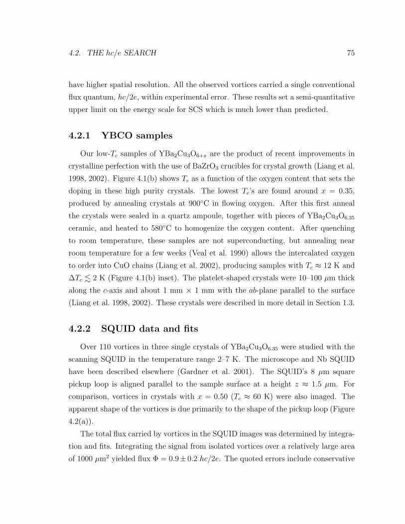
4.2. THE hc/e SEARCH 75
have higher spatial resolution. All the observed vortices carried a single conventional
flux quantum, hc/2e, within experimental error. These results set a semi-quantitative
upper limit on the energy scale for SCS which is much lower than predicted.
4.2.1 YBCO samples
Our low-Tc samples of YBa2Cu3O6+x are the product of recent improvements in
crystalline perfection with the use of BaZrO3 crucibles for crystal growth (Liang et al.
1998, 2002). Figure 4.1(b) shows Tc as a function of the oxygen content that sets the
doping in these high purity crystals. The lowest Tc’s are found around x = 0.35,
produced by annealing crystals at 900C in flowing oxygen. After this first anneal
the crystals were sealed in a quartz ampoule, together with pieces of YBa2Cu3O6.35
ceramic, and heated to 580C to homogenize the oxygen content. After quenching
to room temperature, these samples are not superconducting, but annealing near
room temperature for a few weeks (Veal et al. 1990) allows the intercalated oxygen
to order into CuO chains (Liang et al. 2002), producing samples with Tc ≈ 12 K and
∆Tc . 2 K (Figure 4.1(b) inset). The platelet-shaped crystals were 10–100 µm thick
along the c-axis and about 1 mm × 1 mm with the ab-plane parallel to the surface
(Liang et al. 1998, 2002). These crystals were described in more detail in Section 1.3.
4.2.2 SQUID data and fits
Over 110 vortices in three single crystals of YBa2Cu3O6.35 were studied with the
scanning SQUID in the temperature range 2–7 K. The microscope and Nb SQUID
have been described elsewhere (Gardner et al. 2001). The SQUID’s 8 µm square
pickup loop is aligned parallel to the sample surface at a height z ≈ 1.5 µm. For
comparison, vortices in crystals with x = 0.50 (Tc ≈ 60 K) were also imaged. The
apparent shape of the vortices is due primarily to the shape of the pickup loop (Figure
4.2(a)).
The total flux carried by vortices in the SQUID images was determined by integra-
tion and fits. Integrating the signal from isolated vortices over a relatively large area
of 1000 µm2 yielded flux Φ = 0.9± 0.2 hc/2e. The quoted errors include conservative
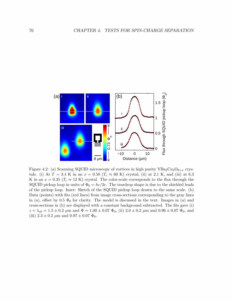
76 CHAPTER 4. TESTS FOR SPIN-CHARGE SEPARATION
(a) i ii
iii
8 µm−10 0 10
0
0.5
1
1.5
(b)
i
ii
iii
Distance (µm)F
lux
thro
ugh
SQ
UID
pic
kup
loop
(Φ0)
0.73
Φ0
Figure 4.2: (a) Scanning SQUID microscopy of vortices in high purity YBa2Cu3O6+x crys-tals. (i) At T = 3.4 K in an x = 0.50 (Tc ≈ 60 K) crystal; (ii) at 2.1 K, and (iii) at 6.3K in an x = 0.35 (Tc ≈ 12 K) crystal. The color-scale corresponds to the flux through theSQUID pickup loop in units of Φ0 = hc/2e. The teardrop shape is due to the shielded leadsof the pickup loop. Inset: Sketch of the SQUID pickup loop drawn to the same scale. (b)Data (points) with fits (red lines) from image cross-sections corresponding to the gray linesin (a), offset by 0.5 Φ0 for clarity. The model is discussed in the text. Images in (a) andcross-sections in (b) are displayed with a constant background subtracted. The fits gave (i)z + λab = 1.5± 0.2 µm and Φ = 1.00± 0.07 Φ0, (ii) 2.0± 0.2 µm and 0.96± 0.07 Φ0, and(iii) 2.3± 0.2 µm and 0.97± 0.07 Φ0.
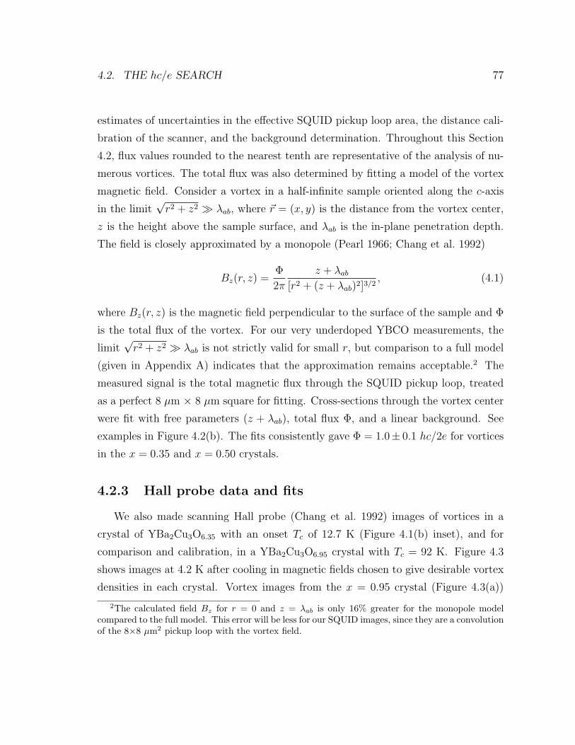
4.2. THE hc/e SEARCH 77
estimates of uncertainties in the effective SQUID pickup loop area, the distance cali-
bration of the scanner, and the background determination. Throughout this Section
4.2, flux values rounded to the nearest tenth are representative of the analysis of nu-
merous vortices. The total flux was also determined by fitting a model of the vortex
magnetic field. Consider a vortex in a half-infinite sample oriented along the c-axis
in the limit√
r2 + z2 À λab, where ~r = (x, y) is the distance from the vortex center,
z is the height above the sample surface, and λab is the in-plane penetration depth.
The field is closely approximated by a monopole (Pearl 1966; Chang et al. 1992)
Bz(r, z) =Φ
2π
z + λab
[r2 + (z + λab)2]3/2, (4.1)
where Bz(r, z) is the magnetic field perpendicular to the surface of the sample and Φ
is the total flux of the vortex. For our very underdoped YBCO measurements, the
limit√
r2 + z2 À λab is not strictly valid for small r, but comparison to a full model
(given in Appendix A) indicates that the approximation remains acceptable.2 The
measured signal is the total magnetic flux through the SQUID pickup loop, treated
as a perfect 8 µm × 8 µm square for fitting. Cross-sections through the vortex center
were fit with free parameters (z + λab), total flux Φ, and a linear background. See
examples in Figure 4.2(b). The fits consistently gave Φ = 1.0± 0.1 hc/2e for vortices
in the x = 0.35 and x = 0.50 crystals.
4.2.3 Hall probe data and fits
We also made scanning Hall probe (Chang et al. 1992) images of vortices in a
crystal of YBa2Cu3O6.35 with an onset Tc of 12.7 K (Figure 4.1(b) inset), and for
comparison and calibration, in a YBa2Cu3O6.95 crystal with Tc = 92 K. Figure 4.3
shows images at 4.2 K after cooling in magnetic fields chosen to give desirable vortex
densities in each crystal. Vortex images from the x = 0.95 crystal (Figure 4.3(a))
2The calculated field Bz for r = 0 and z = λab is only 16% greater for the monopole modelcompared to the full model. This error will be less for our SQUID images, since they are a convolutionof the 8×8 µm2 pickup loop with the vortex field.
78 CHAPTER 4. TESTS FOR SPIN-CHARGE SEPARATION
(a)
10 µm
(b)
10 µm
I
1.3
G
Figure 4.3: Scanning Hall probe images of hc/2e vortices in YBa2Cu3O6+x crystals at 4.2K with line by line background subtraction. (a) In a nearly optimally doped sample withx = 0.95 and Tc = 92 K. Inset: The Hall probe at the same scale, with the direction of theAC current (I ) as shown. (b) In a very underdoped sample with x = 0.35 and Tc = 12.7 K.The density of vortices was determined by the applied field when cooled. Note the lowerpeaks and wider profiles of the vortices in (b) compared to (a).
appear to be resolution-limited, consistent with the known low temperature pene-
tration depth in similar near-optimally doped samples, λab ≈ 0.16 µm (Basov et al.
1995). Fits to the vortex images in that sample were therefore used to characterize
the size and shape of the nominally 2 µm× 2 µm Hall probe (shown in Figure 4.3(a)
inset). The images in Figure 4.3 were obtained on adjacent, aligned, flat samples in
an attempt to have a constant z ≈ 1 µm.
Although the Hall probe measurement had more background and less field sen-
sitivity than the SQUID measurement (making averaging necessary), the Hall probe
was crucial for a thorough survey of vortices in the very underdoped samples, since
hc/e vortices should be most stable close to Tc (Sachdev 1992; Nagaosa and Lee 1992;
Nagaosa 1994; Senthil and Fisher 2001a), as schematically shown in Figure 4.1(a). We
imaged vortices formed after cooling just below the Tc = 12.7 K of the YBa2Cu3O6.35
sample. This addressed a scenario in which energetically favored hc/e vortices might
not form if hc/2e vortices, which repel each other, were already present. Often we
continued cooling and imaged the vortices for T as low as 3 K, and then warmed and
imaged again just below Tc. The vortex locations did not change with this tempera-
ture cycling below Tc, indicating that vortices neither split nor condensed, and thus
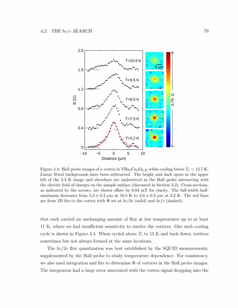
4.2. THE hc/e SEARCH 79
−10 −5 0 5 10
0
0.4
0.8
1.2
1.6
2.0
T=10.5 K
T=9.5 K
T=8.5 K
T=7.5 K
T=3.2 K
Distance (µm)
B (
G)
→ ←
5 µm
→ ←
→ ←
→ ←
→ ←
0.79
GFigure 4.4: Hall probe images of a vortex in YBa2Cu3O6.35 while cooling below Tc = 12.7 K.Linear fitted backgrounds have been subtracted. The bright and dark spots in the upperleft of the 3.2 K image and elsewhere are understood as the Hall probe interacting withthe electric field of charges on the sample surface (discussed in Section 3.2). Cross-sections,as indicated by the arrows, are shown offset by 0.04 mT for clarity. The full-width half-maximum decreases from 5.3 ± 0.3 µm at 10.5 K to 4.0 ± 0.3 µm at 3.2 K. The red linesare from 2D fits to the vortex with Φ set at hc/2e (solid) and hc/e (dashed).
that each carried an unchanging amount of flux at low temperatures up to at least
11 K, where we had insufficient sensitivity to resolve the vortices. One such cooling
cycle is shown in Figure 4.4. When cycled above Tc to 15 K and back down, vortices
sometimes but not always formed at the same locations.
The hc/2e flux quantization was best established by the SQUID measurements,
supplemented by the Hall probe to study temperature dependence. For consistency,
we also used integration and fits to determine Φ of vortices in the Hall probe images.
The integration had a large error associated with the vortex signal dropping into the
80 CHAPTER 4. TESTS FOR SPIN-CHARGE SEPARATION
noise quickly, potentially losing tenths of a flux quantum. Single vortex integration
gave Φ = 0.7 to 0.9 hc/2e in the near-optimally doped sample, where vortices are
known to be hc/2e, and Φ = 0.6 to 0.8 hc/2e in the x = 0.35 sample for T . 10 K. In
both cases, conservatively estimating the error in background determination to be its
standard deviation gives an error <0.6 hc/2e for Φ, and estimating a maximum error
of 20% in the scanner area calibration gives error 0.13 hc/2e. Hall probe images of
isolated vortices were also fit in two dimensions to Equation (4.1) with free parameters
(z + λab), Φ, and a planar background. The best fits in the x = 0.35 sample gave
total flux Φ primarily from 0.8 to 1.1 hc/2e for T < 10 K, and from 0.6 to 1.0 hc/2e
for ∼11 K. Systematic errors dominate, such as the high correlation between the
parameters (z+λab) and Φ, the planar background fit, and the validity of the monopole
model near Tc. An estimate of ±0.2 µm for the error in (z + λab) gives error bars
≤0.11 hc/2e for Φ, while the latter sources of error are more difficult to quantify. Fits
with Φ fixed at hc/2e and at hc/e clearly show hc/2e as the better fit (Figure 4.4).
In all, we observed 60 vortices with the Hall probe in the very underdoped YBCO
sample.
The Hall probe images show apparent vortex spreading in YBa2Cu3O6.35 compared
to the near-optimally doped crystal (Figure 4.3) that may be due to a penetration
depth that is not negligible compared to the 2 µm Hall probe. Alternative hypotheses
include vortex bending, fast vortex motion confined to a micron-scale region, or a
non-superconducting layer on the crystal surface. The images in Figure 4.4 show the
temperature dependent vortex spreading in the very underdoped YBCO, consistent
with a λab(T ) that increases with temperature. The full-width half-maximum of a
vortex image in the x = 0.95 sample is 3.0 ± 0.3 µm (resolution-limited), while in
the x = 0.35 sample it is 4.0 ± 0.3 µm at 3.2 K and 5.3 ± 0.3 µm at 10.5 K. From
these numbers, and from the 2D fits with (z + λab) as a free parameter, we interpret
the major source of vortex spreading in the x = 0.35 YBCO as a penetration depth
λab & 1 µm which increases with temperature. This inferred λab is somewhat larger
than expected from higher-Tc extrapolations (Uemura et al. 1989). A more thorough
and quantitative study of λab as a function of doping in underdoped cuprates is
possible with higher resolution Hall probes, and is the subject of Chapter 5.
4.2. THE hc/e SEARCH 81
4.2.4 Discussion
Overall, we saw no hc/e vortices in SQUID and Hall probe images of more than
170 vortices in YBa2Cu3O6.35. This result sets limits on scenarios of spin-charge
separation; in particular, we set an upper limit on the vison energy in the Senthil-
Fisher formulation. They propose that Evison ≈ kBT ∗ (per 2D superconducting layer)
(Senthil and Fisher 2001a,b). In usual Ginzburg-Landau theory, the energy per unit
length of an nhc/2e vortex is given by Enhc/2e = Enhc/2esf + E
nhc/2ecore , where
Enhc/2esf =
(nhc/2e
4πλab
)2
ln(λab/ξ) (4.2)
is the superfluid energy, n is an integer, ξ is the coherence length, and Ecore is small
compared to Esf (Tinkham 1996, p. 153–4). The vison can be cast as an excess
core energy for an hc/2e vortex (Senthil and Fisher 2001a). Thus we write Ehc/2e =
Ehc/2esf +Ecore +Evison, while Ehc/e = 4E
hc/2esf +Ecore. The most natural interpretation
of our observations of only hc/2e vortices is that 2Ehc/2e < Ehc/e, and therefore
Evison < Ehc/2esf (neglecting pinning energy3). Conservatively using λab ≈ 1 µm and
taking ln(λab/ξ) ≈ 5, we set an upper limit on the excess core energy associated with
an hc/2e vortex: Evison/kB < 60 K.4
In the context of the Senthil-Fisher predictions, the significance of this upper limit
depends on the exact value of T ∗, which will be difficult to measure in these very
underdoped samples because the dopant oxygens disorder above room temperature.
Early NMR measurements indicate that T ∗ exceeds 300 K in YBa2Cu3O6.48 (Alloul
et al. 1989). A more recent interpretation of the T ∗ energy scale indicates values as
high as 500–700 K in very underdoped samples (Tallon and Loram 2001). Thus our
upper bound on the vison energy is much below the predicted value. To reconcile
this result with the predictions would require a superconducting transition which is
3With vortex pinning, Enhc/2e has an additional term −Enhc/2epin . Pinning potentials in high
purity crystals may arise from small spatial variations in the doping. Epin of a traditional vortexshould be at most ∼Ecore, while here E
hc/2epin could include a vison contribution Evison
pin . Since intheory Evison ≈ kBT ∗, Evison
pin due to doping variations should be much smaller than Evison. Thus
our energy balance expression becomes Evison − Evisonpin ≈ Evison < E
hc/2esf as before.
4Evison/kB < 120 K if there is one vison per unit cell instead of per copper-oxide plane.
82 CHAPTER 4. TESTS FOR SPIN-CHARGE SEPARATION
strongly first-order (Sachdev 1992; Senthil and Fisher 2001a), or a theoretical model of
vortex formation that does not permit hc/e vortices even when they are energetically
preferred (Senthil and Fisher 2001a). We tested one such model by imaging vortices
after cooling just below Tc. Senthil and Fisher also proposed an ingenious experiment
to address the dynamics issue by trapping a vison in a hole in a cuprate cylinder
(Senthil and Fisher 2001b). These experiments have been done (Bonn et al. 2001;
Kirtley et al. 2001), see Section 4.3.
In the overall context of cuprate superconductivity, this work has extended exper-
imental studies of single magnetic flux quanta into a new part of the phase diagram
which was first theoretically explored a decade ago (Sachdev 1992; Nagaosa and Lee
1992). Further vortex imaging in these very underdoped samples have allowed mea-
surements of the apparent size of a vortex (an upper limit on the in-plane penetration
depth) as a function of temperature and doping (Chapter 5), and studies of single
vortex dynamics and energetics.
4.3 The vortex memory experiment5
A more stringent test for spin-charge separation in the cuprates is an elegant
experiment devised by Senthil and Fisher (2001b) which tests for clear signatures
of the proposed topological defects known as visons. The experiment address the
dynamic nature of the vison, and thus interpretation of the results is not restricted
by caveats of metastability as in the hc/e search discussed above. In this section I
report our results of these experimental tests, which conservatively placed an upper
limit of 190 K on the vison energy.
4.3.1 Experimental proposal
To test their theory of SCS, Senthil and Fisher (2001b) proposed a “smoking gun”
experiment in which a vison is trapped in a ring made from a cuprate superconductor.
Figure 4.5, as well as the inset to Figure 4.6, summarizes the experiment. The ring
5This vortex memory experiment was published as Bonn et al. (2001).
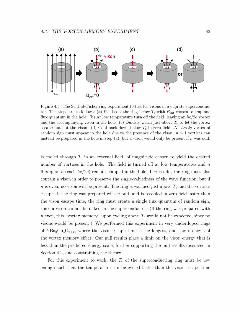
4.3. THE VORTEX MEMORY EXPERIMENT 83
or
Bext=0
vison
Bext
(a) (b) (c) (d)
Figure 4.5: The Senthil–Fisher ring experiment to test for visons in a cuprate superconduc-tor. The steps are as follows: (a) Field cool the ring below Tc with Bext chosen to trap oneflux quantum in the hole. (b) At low temperature turn off the field, leaving an hc/2e vortexand the accompanying vison in the hole. (c) Quickly warm just above Tc to let the vortexescape but not the vison. (d) Cool back down below Tc in zero field. An hc/2e vortex ofrandom sign must appear in the hole due to the presence of the vison. n > 1 vortices caninstead be prepared in the hole in step (a), but a vison would only be present if n was odd.
is cooled through Tc in an external field, of magnitude chosen to yield the desired
number of vortices in the hole. The field is turned off at low temperatures and n
flux quanta (each hc/2e) remain trapped in the hole. If n is odd, the ring must also
contain a vison in order to preserve the single-valuedness of the wave function; but if
n is even, no vison will be present. The ring is warmed just above Tc and the vortices
escape. If the ring was prepared with n odd, and is recooled in zero field faster than
the vison escape time, the ring must create a single flux quantum of random sign,
since a vison cannot be naked in the superconductor. (If the ring was prepared with
n even, this “vortex memory” upon cycling above Tc would not be expected, since no
visons would be present.) We performed this experiment in very underdoped rings
of YBa2Cu3O6+x, where the vison escape time is the longest, and saw no signs of
the vortex memory effect. Our null results place a limit on the vison energy that is
less than the predicted energy scale, further supporting the null results discussed in
Section 4.2, and constraining the theory.
For this experiment to work, the Tc of the superconducting ring must be low
enough such that the temperature can be cycled faster than the vison escape time
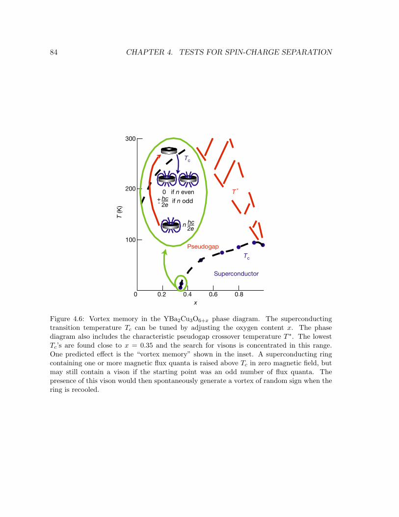
84 CHAPTER 4. TESTS FOR SPIN-CHARGE SEPARATION
c
c
Figure 4.6: Vortex memory in the YBa2Cu3O6+x phase diagram. The superconductingtransition temperature Tc can be tuned by adjusting the oxygen content x. The phasediagram also includes the characteristic pseudogap crossover temperature T ∗. The lowestTc’s are found close to x = 0.35 and the search for visons is concentrated in this range.One predicted effect is the “vortex memory” shown in the inset. A superconducting ringcontaining one or more magnetic flux quanta is raised above Tc in zero magnetic field, butmay still contain a vison if the starting point was an odd number of flux quanta. Thepresence of this vison would then spontaneously generate a vortex of random sign when thering is recooled.
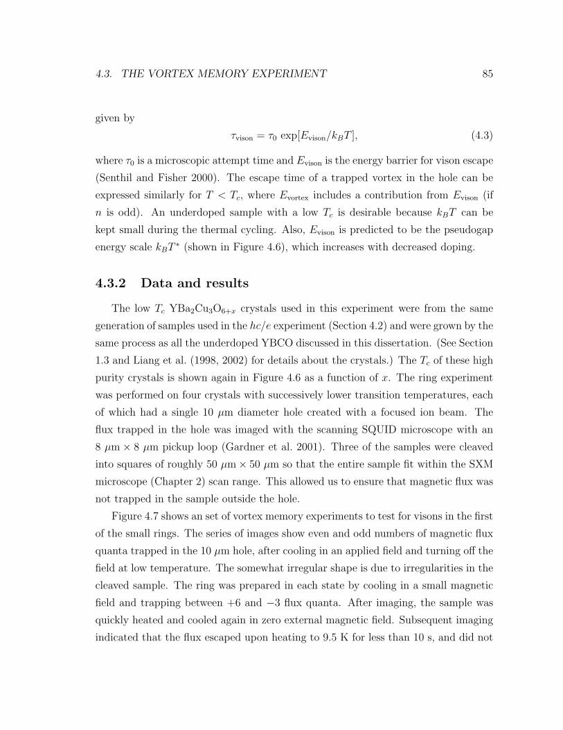
4.3. THE VORTEX MEMORY EXPERIMENT 85
given by
τvison = τ0 exp[Evison/kBT ], (4.3)
where τ0 is a microscopic attempt time and Evison is the energy barrier for vison escape
(Senthil and Fisher 2000). The escape time of a trapped vortex in the hole can be
expressed similarly for T < Tc, where Evortex includes a contribution from Evison (if
n is odd). An underdoped sample with a low Tc is desirable because kBT can be
kept small during the thermal cycling. Also, Evison is predicted to be the pseudogap
energy scale kBT ∗ (shown in Figure 4.6), which increases with decreased doping.
4.3.2 Data and results
The low Tc YBa2Cu3O6+x crystals used in this experiment were from the same
generation of samples used in the hc/e experiment (Section 4.2) and were grown by the
same process as all the underdoped YBCO discussed in this dissertation. (See Section
1.3 and Liang et al. (1998, 2002) for details about the crystals.) The Tc of these high
purity crystals is shown again in Figure 4.6 as a function of x. The ring experiment
was performed on four crystals with successively lower transition temperatures, each
of which had a single 10 µm diameter hole created with a focused ion beam. The
flux trapped in the hole was imaged with the scanning SQUID microscope with an
8 µm × 8 µm pickup loop (Gardner et al. 2001). Three of the samples were cleaved
into squares of roughly 50 µm× 50 µm so that the entire sample fit within the SXM
microscope (Chapter 2) scan range. This allowed us to ensure that magnetic flux was
not trapped in the sample outside the hole.
Figure 4.7 shows an set of vortex memory experiments to test for visons in the first
of the small rings. The series of images show even and odd numbers of magnetic flux
quanta trapped in the 10 µm hole, after cooling in an applied field and turning off the
field at low temperature. The somewhat irregular shape is due to irregularities in the
cleaved sample. The ring was prepared in each state by cooling in a small magnetic
field and trapping between +6 and −3 flux quanta. After imaging, the sample was
quickly heated and cooled again in zero external magnetic field. Subsequent imaging
indicated that the flux escaped upon heating to 9.5 K for less than 10 s, and did not
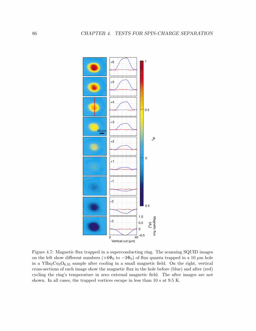
86 CHAPTER 4. TESTS FOR SPIN-CHARGE SEPARATION
letters to nature
888 NATURE |VOL 414 | 20/27 DECEMBER 2001 |www.nature.com
magnetic ¯ux in the superconducting state. If the number oftrapped ¯ux quanta is odd, the ring will also contain a vison thatcould persist above Tc. If the ring is recooled in zero ®eld before thevison escapes, it will spontaneously generate a single ¯ux quantumof random sign. (A ring prepared with an even number of ¯uxquanta would not contain a vison, and would not exhibit this`vortex memory' after cycling the temperature.) We have seen nosign of the vortex-memory effect in the experiments reported here,placing a limit on the stability of visons and constraining the use of aclass of spin±charge separation theories to explain the unusualproperties of the copper oxides.The experiment requires a ring with a Tc that is low enough to
allow the sample temperature to be cycled faster than the visonescape time tv, expressed as
tv t0 expEvison=kBT 1
where t0 is a microscopic attempt time, and Evison is the energy
barrier for vison escape4. Below Tc, the lifetime of a trapped ¯uxquantum can be expressed similarly, with a characteristic energyEvortex that includes a contribution from Evison if the number oftrapped quanta is odd. An underdoped sample with a low Tc meansthat the thermal energy kBT can be kept small throughout thethermal cycling. Low doping also helps by increasing Evison, which ispredicted4 to be the pseudogap energy scale kBT* (Fig. 1).The low-Tc samples of YBa2Cu3O6+x used in this study have
improved crystalline quality, obtained by using BaZrO3 crucibles forcrystal growth9. Figure 1 shows theTc of these high-purity crystals asa function of the oxygen content that sets the doping. The experi-ment was performed on a series of four crystals with successivelylower transition temperatures, each having a single 10-mm-diameter hole fabricated with a focused ion beam. The trappedmagnetic ¯ux was imaged with a scanning SQUID magnetometerwith a square (8mm ´ 8mm) Nb pickup loop and a 70-mm scanrange at 4 K (ref. 10). Three of the samples were cleaved into squaresof roughly 50mm´ 50mm, so that it was possible to image the entiresample and ensure that magnetic ¯ux was not trapped outside the10-mm hole. Both sample and magnetometer were mounted in ahelium-¯ow cryostat surrounded by three layers of mu-metalshielding and an electromagnet used to apply small ®elds.Figure 2 shows an ensemble of experiments to test for the vortex
`memory' associated with visons in the ®rst of the small rings. Theimages on the left are of magnetic ¯ux trapped in the 10-mm hole.The somewhat irregular shape is due to irregularities in the cleavedsample. The ring was prepared in each state by cooling in a smallmagnetic ®eld, trapping between +6 and -3 ¯ux quanta. Afterimaging, the sample was quickly heated and cooled again in zeroexternal magnetic ®eld. Subsequent imaging indicated that the¯ux escapes upon heating to 9.5 K for less than 10 s, and doesnot reappear. There was also no dependence on whether thestarting condition involved an even or odd number of trapped¯ux quanta.A more stringent search involved a pair of samples annealed to
+2
0
10 µm
+6
+5
+4
+3
+1
–1
–2
–0.5
0
0.5
1.0
–3
0.5
0 40
Vertical cut (µm)
0
0.5
1
Φ(
0 )
Mag
netic
flux
Φ
Figure 2 Magnetic ¯ux trapped in a superconducting ring. The scanning SQUID
magnetometer images to the left show different numbers (+6©0 to -3©0) of ¯ux quanta
trapped in a hole in a YBa2Cu3O6.35 sample by cooling in a small magnetic ®eld. The colour
indicates the ¯ux through a square (8mm ´ 8mm) pickup loop. On the right, vertical
cross-sections of the images show the magnetic ¯ux in the hole before (blue) and after
(red) cycling the ring's temperature in zero external magnetic ®eld. In all cases, the
trapped vortices escape in less than 10 s at 9.5 K.
10 µm
Vertical cut (µm)
00
0.10.1
0.2
0.2
0.3
Φ
0 20 40
0
Mag
netic f
lux (
0)
Φ
Figure 3 Cross-sections and images of ¯ux quanta trapped in a ring with Tc = 6.0 K. The
upper right image shows the typical geometry of the rings used in the experiment; they are
squares (50mm´ 50mm) of single-crystal YBa2Cu3O6.35, with a 10-mmhole drilled using
a focused ion beam. The middle and lower right images shows double (2©0) and single
(©0) ¯ux quanta trapped in the ring. Integration of the total ¯ux in the images con®rms that
the ¯ux quantization is©0 = h/2e. The cross-sections shown on the left are obtained from
20-pixel-wide vertical stripes through the images, with the 20 pixels averaged in order to
reduce noise and carefully con®rm the reproducibility of the ¯ux quanta. The many cross-
sections show that single and double ¯ux quanta (blue and red curves, respectively) could
be repeatedly generated in the ring, although there were also numerous instances where
some of the ¯ux appeared to `leak' into the annulus of the ring, a possible indication of
granular behaviour. When the ring was heated in null ®eld to only 5.6 K for 1 s, then
recooled to 2 K, imaging indicated that these ¯ux quanta escape with no sign of the vortex
memory associated with visons.
© 2001 Macmillan Magazines Ltd
Figure 4.7: Magnetic flux trapped in a superconducting ring. The scanning SQUID imageson the left show different numbers (+6Φ0 to −3Φ0) of flux quanta trapped in a 10 µm holein a YBa2Cu3O6.35 sample after cooling in a small magnetic field. On the right, verticalcross-sections of each image show the magnetic flux in the hole before (blue) and after (red)cycling the ring’s temperature in zero external magnetic field. The after images are notshown. In all cases, the trapped vortices escape in less than 10 s at 9.5 K.
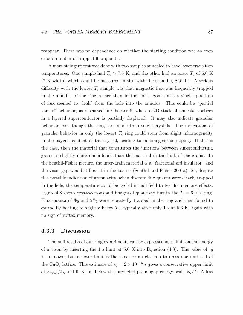
4.3. THE VORTEX MEMORY EXPERIMENT 87
reappear. There was no dependence on whether the starting condition was an even
or odd number of trapped flux quanta.
A more stringent test was done with two samples annealed to have lower transition
temperatures. One sample had Tc ≈ 7.5 K, and the other had an onset Tc of 6.0 K
(2 K width) which could be measured in situ with the scanning SQUID. A serious
difficulty with the lowest Tc sample was that magnetic flux was frequently trapped
in the annulus of the ring rather than in the hole. Sometimes a single quantum
of flux seemed to “leak” from the hole into the annulus. This could be “partial
vortex” behavior, as discussed in Chapter 6, where a 2D stack of pancake vortices
in a layered superconductor is partially displaced. It may also indicate granular
behavior even though the rings are made from single crystals. The indications of
granular behavior in only the lowest Tc ring could stem from slight inhomogeneity
in the oxygen content of the crystal, leading to inhomogeneous doping. If this is
the case, then the material that constitutes the junctions between superconducting
grains is slightly more underdoped than the material in the bulk of the grains. In
the Senthil-Fisher picture, the inter-grain material is a “fractionalized insulator” and
the vison gap would still exist in the barrier (Senthil and Fisher 2001a). So, despite
this possible indication of granularity, when discrete flux quanta were clearly trapped
in the hole, the temperature could be cycled in null field to test for memory effects.
Figure 4.8 shows cross-sections and images of quantized flux in the Tc = 6.0 K ring.
Flux quanta of Φ0 and 2Φ0 were repeatedly trapped in the ring and then found to
escape by heating to slightly below Tc, typically after only 1 s at 5.6 K, again with
no sign of vortex memory.
4.3.3 Discussion
The null results of our ring experiments can be expressed as a limit on the energy
of a vison by inserting the 1 s limit at 5.6 K into Equation (4.3). The value of τ0
is unknown, but a lower limit is the time for an electron to cross one unit cell of
the CuO2 lattice. This estimate of τ0 = 2 × 10⁻¹⁵ s gives a conservative upper limit
of Evison/kB < 190 K, far below the predicted pseudogap energy scale kBT ∗. A less
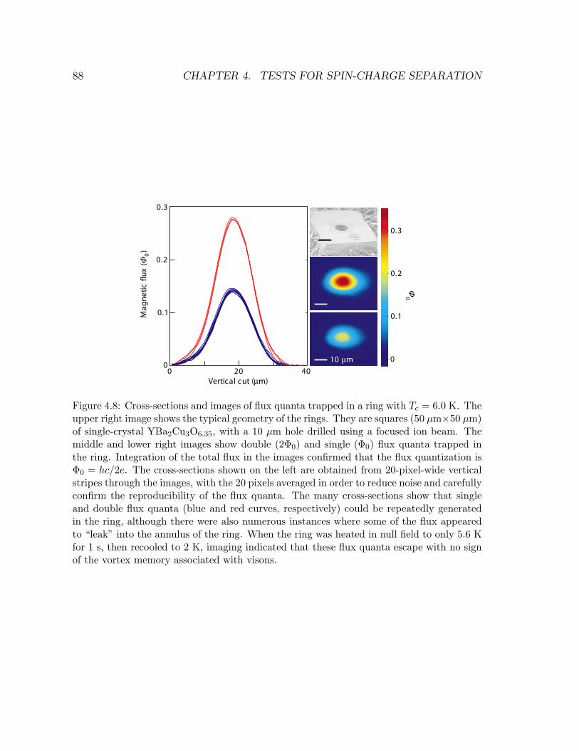
88 CHAPTER 4. TESTS FOR SPIN-CHARGE SEPARATION
10 µm
Vertical cut (µm)
00
0.10.1
0.2
0.2
0.3
Φ
0 20 40
0
Ma
gn
eti
cfl
ux
(0
)Φ
0.3
Figure 4.8: Cross-sections and images of flux quanta trapped in a ring with Tc = 6.0 K. Theupper right image shows the typical geometry of the rings. They are squares (50 µm×50 µm)of single-crystal YBa2Cu3O6.35, with a 10 µm hole drilled using a focused ion beam. Themiddle and lower right images show double (2Φ0) and single (Φ0) flux quanta trapped inthe ring. Integration of the total flux in the images confirmed that the flux quantization isΦ0 = hc/2e. The cross-sections shown on the left are obtained from 20-pixel-wide verticalstripes through the images, with the 20 pixels averaged in order to reduce noise and carefullyconfirm the reproducibility of the flux quanta. The many cross-sections show that singleand double flux quanta (blue and red curves, respectively) could be repeatedly generatedin the ring, although there were also numerous instances where some of the flux appearedto “leak” into the annulus of the ring. When the ring was heated in null field to only 5.6 Kfor 1 s, then recooled to 2 K, imaging indicated that these flux quanta escape with no signof the vortex memory associated with visons.
4.4. SUMMARY AND THE FUTURE OF SCS 89
conservative lower bound on τ0 that is commonly used in discussions of vortex creep in
conventional superconductors is τ0 = 10−12 s, based on the characteristic frequencies
of lattice vibrations (Beasley et al. 1969). This higher estimate of τ0 would give an
upper limit of Evison/kB < 160 K.
These ring experiments give a larger upper limit on Evison than the observations
of only hc/2e static vortices in these samples discussed in Section 4.2. But the vortex
memory experiment is a stricter test for visons, since it could be that the hc/2e
vortices in the earlier experiment were metastable. Measuring two steady states
in the ring experiment (before and after thermal cycling) gives information on the
dynamics, and thus also the energy scale, of possible trapped visons. The limit of
Evison/kB < 190 K restricts any role that visons might have in the physics of these
materials in the underdoped regime.
4.4 Summary and the future of SCS
We conducted two experimental tests for a promising microscopic formulation of
spin-charge separation (Senthil and Fisher 2000) in the underdoped cuprate super-
conductors. Both tests utilized the flux imaging capabilities of our scanning SQUID
and scanning Hall probe microscope, and were made possible by the recent progress
in the growth and preparation of high quality very underdoped single crystals of
YBa2Cu3O6+x (Liang et al. 2002). In the first experiment we saw no evidence of
hc/e vortices in very underdoped YBCO samples, though hc/e vortices are predicted
by SCS for very underdoped cuprates. We also performed an experiment proposed
by Senthil and Fisher (2001b) but saw no vortex memory effect, which would have
been the signature of visons, the topological defects of the Senthil-Fisher SCS theory.
The first experiment set a limit of Evison/kB < 60 K, while the more stringent vortex
memory experiment set a strict limit of Evison/kB < 190 K. Both of these limits are
much less than the predicted vison energy scale Evison ≈ kBT ∗ (Senthil and Fisher
2001a). Together our experiments make unlikely any SCS scenarios for the cuprates
which require visons.
SCS scenarios for the cuprates have not been abandoned however. Paramekanti
90 CHAPTER 4. TESTS FOR SPIN-CHARGE SEPARATION
et al. (2002) propose a new model of an “exciton Bose liquid” in which bosonic
Cooper pairs on a square lattice interact via ring exchange. They call their model a
“middle ground” between a Mott insulator and the fully fractionalized SCS scenario.
Ribeiro and Wen (2003) predict that there will be no fractionalization in hole-doped
cuprates (such as YBCO), but they show that SCS is a candidate for the metallic
pseudogap phase of electron-doped cuprates. Experimental studies on electron-doped
cuprates are needed to test this possibility. Other theoretical work by Paramekanti
et al. (2003) calculates that the vison gap in the cuprates could be much smaller
than in the original Senthil and Fisher (2001a) formulation. They state that Evison
could be .50 K, which would mean fractionalization would only appear at very low
temperatures and thus could not be responsible for the properties of the pseudogap.
Though the outlook for SCS in the cuprates is dubious, there is interest currently
in the strong possibility of fractionalization in highly frustrated magnets. Coldea
et al. (2001) saw evidence for a 2D fractional spin liquid in neutron scattering mea-
surements on the frustrated antiferromagnet Cs2CuCl4. Senthil and Motrunich (2002)
construct microscopic models of fractionalized phases and show that it is possible to
have a SCS magnetic phase. Chung et al. (2003) examined the Cs2CuCl4 system
theoretically. They computed models for both bosonic and fermionic6 spin liquid
states which predict different temperature dependent behavior for neutron scattering
measurements. Further experiments are needed to determine which type fractional-
ization exists in the magnetically frustrated Cs2CuCl4 system. Frustrated magnets
are promising candidates for 2D fractionalization because the inherent frustration
leads to deconfinement of the antiferromagnetic spins.
6The spin-charge separation tested for cuprates in this chapter is of the fermionic sort, since thespinon had spin 1/2.
Chapter 5
Penetration depth measurements
The submicron scanning Hall probe microscope and the newly available extremely
underdoped superconducting YBa2Cu3O6+x (YBCO) single crystals from UBC (Liang
et al. 2002) enable studies of magnetic vortices in the very underdoped region of the
cuprate phase diagram (Figure 1.1). This region of very small superfluid density is
theoretically important but until recently remained unexplored experimentally due to
the absence of good samples with sharp superconducting transitions. In this chapter
I discuss my attempts to measure the in-plane penetration depth (λab) in the very
underdoped YBCO.
This chapter first introduces the penetration depth (λ), summarizes various meth-
ods used to measure λ in the literature, and introduces the widely accepted “Uemura
relation” that Tc ∝ 1/λ2(0). Then I detail my Hall probe imaging studies of indi-
vidual vortices in a very underdoped YBa2Cu3O6.375 crystal, which had a variable Tc
from 5 to 15 K. Fits of my images to a model of the vortex field profile allowed the
size of the vortex to be measured. The size (as I am defining it) of a traditional 3D
vortex is λab, though in these anisotropic crystals it is possible that staggered pinning
of 2D pancake vortices contribute to the measured apparent size. If staggered pinning
is not the case, my results suggest a larger penetration depth than predicted by the
Uemura relation for at least Tc ≤ 6.5 K.
91
92 CHAPTER 5. PENETRATION DEPTH MEASUREMENTS
5.1 Introduction
An important parameter of a superconductor is the magnetic penetration depth.
It is the length scale over which external magnetic fields penetrate the superconductor
and are exponentially screened. In the vortex state λ determines the extent or size of
the vortices, that is, the length over which the vortex magnetic field and supercurrent
fall off. The penetration depth is directly related to the superfluid density, ns/m∗, by
the relation ns/m∗ = (c2/4πe2)λ−2, where ns is the superconducting carrier density
and m∗ is the effective mass.1 The superfluid density is a parameter of great theoret-
ical importance. Its value and dependence on doping and temperature allow theories
of superconductivity to be tested and formulated. This is of particular importance
in the high-Tc cuprate superconductors where the mechanism of superconductivity is
not yet understood.
In anisotropic superconductors, such as the cuprates, the penetration depth and
m∗ are direction dependent. The superconductor in this case can be described by
an anisotropic version of the London model with λa, λb, and λc associated with the
abc crystal axes. (The YBCO crystal structure was shown in Figure 1.11.) λa is
the decay length for supercurrent flowing in the a direction, similarly for b and c.
In terms of magnetic field, if B (either external or from a vortex) points along the
c-axis, λa is the distance the field penetrates in the b direction, and λb is the distance
the field penetrates in the a direction. This statement holds for cyclic permutations
abc → bca → cab. In cuprates, λc is large compared to λa and λb, while λa ∼ λb and
they are often referred to collectively as the in-plane penetration depth λab =√
λaλb.
5.1.1 Methods of measuring λ
The absolute value of the penetration depth is difficult to measure. There is
no universal easy method to do so, though several classes of techniques have been
developed, each of which have advantages and drawbacks. Broadly, the techniques
1The literature is not consistent in defining the term superfluid density. Emery and Kivelson(1995a) define it as ns, Pereg-Barnea et al. (2003) define it as ns/m∗, and Tallon et al. (2003) defineit as λ−2.
5.1. INTRODUCTION 93
are those that measure λ by examining (1) the magnetic susceptibility in the Meissner
state, (2) transmission and spectroscopy, or (3) the field distribution in the vortex
state. I will briefly discuss the predominant techniques below. In this chapter I fit
the field profiles of isolated c-axis vortices at the sample surface in an attempt to
measure λab in very underdoped YBa2Cu3O6+x. Though there are caveats to this
measurement, namely I have actually measured the apparent vortex size which could
have contributions besides λab.
Magnetic susceptibility techniques can very accurately measure penetration depth
relative to a base temperature: ∆λ(T ) = λ(T )− λ(Tbase). This has been done at DC
(Krusin-Elbaum et al. 1989), microwave (Hardy et al. 1993), and radio frequencies
(Carrington et al. 1999). Cavity and planar resonators have both been used for the
AC measurements. As the penetration depth changes (e.g. with T ), the volume of the
sample which is superconducting changes, and thus very accurate ∆λ measurements
can be made. However, the absolute penetration depth is difficult to obtain via these
methods, since it would require unrealistically precise knowledge of the sample dimen-
sions. An exception is for very large penetration depths, such as the recent microwave
cavity measurements of absolute λc in underdoped YBa2Cu3O6+x by Hosseini et al.
(2003).
An improved approach to the planar resonator technique has been implemented by
Talanov et al. (2000) which does allow absolute measurement of λ. In their apparatus,
a parallel plate resonator is composed of either the thin film or bulk superconductors
in which λ is to be measured. The key feature of their apparatus is that the spacing
between the parallel plates can be continuously varied with known spacing. The
resonant frequency is dependent on the penetration depth and the spacing, and thus
λ can be determined from fits to the experimentally measured resonant frequency as
a function of spacing.
Pereg-Barnea et al. (2003) at UBC have devised a new microwave technique for
measuring absolute values of the three λ components from the Meissner state. They
grew single crystals of YBa2Cu3O6+x with 1% of the Y3+ ions randomly replaced by
magnetic Gd3+ ions. Measurements of the electron spin resonance (ESR) of the Gd
atoms in an applied microwave field reveals the number of Gd in the field. Since only
94 CHAPTER 5. PENETRATION DEPTH MEASUREMENTS
the Gd within one penetration depth are exposed to the field, the penetration depth
on all three axes can be found from the ESR measurement.
A successful transmission technique for measuring λ involves measuring the mutual
inductance of two coaxial coils separated by a thin film superconductor (Fiory et al.
1988; Lee et al. 1994). This method is restricted to thin films, and the film thickness
and uniformity must be know for an accurate result. Infrared spectroscopy (Basov
et al. 1995) has also been used to measure λ and is not restricted to thin films. Each
component of the penetration depth (λa, λb, and λc) can be measured independently.
Infrared spectroscopy is a challenging technique and requires measurement over a
very large frequency range to obtain the λ results.
Muon spin resonance (µSR) is a technique that measures λ from the magnetic
field distribution inside a superconductor in the vortex state. Polarized muons are
implanted in a sample and the precession of the muon spin depends on the local
magnetic field. The muon decays into two neutrinos and a positron, and the direction
of the positron emission is dependent on the direction of the instantaneous muon spin
polarization at the time of decay. Thus by detecting the emitted positrons, the
distribution of magnetic field in the sample can be probed. Since the field profile
of the vortex lattice depends on the bulk penetration depth, λ can be determined
from fits to the µSR data. For a thorough review of µSR applied to the vortex
state, see Sonier et al. (2000). µSR cannot measure the penetration depth for a
single axis, rather it measures a mean such as λab. The µSR measurement of λ
depends on having a detailed model of the magnetic fields of the vortex lattice. Also,
at high fields the measured λ can differ from the Meissner state λ. The assumed
model for the magnetic field distribution, the geometry of the vortex lattice, and
twinning boundaries can each contribute errors to the absolute measurement of λab,
but measurements of dλab/dT are relatively unaffected by these uncertainties (Sonier
et al. 2000). The µSR technique is also limited to measuring λ . 1 µm (Uemura
et al. 1991).
All of the above techniques have advantages and disadvantages, and rely to varying
extents on underlying models in order to measure the penetration depth. Some of the
techniques cannot measure the absolute value of λ, or cannot isolate the components
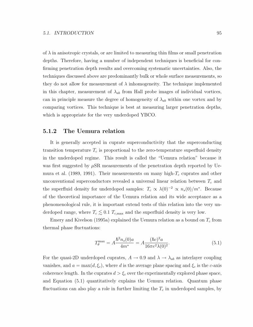
5.1. INTRODUCTION 95
of λ in anisotropic crystals, or are limited to measuring thin films or small penetration
depths. Therefore, having a number of independent techniques is beneficial for con-
firming penetration depth results and overcoming systematic uncertainties. Also, the
techniques discussed above are predominantly bulk or whole surface measurements, so
they do not allow for measurement of λ inhomogeneity. The technique implemented
in this chapter, measurement of λab from Hall probe images of individual vortices,
can in principle measure the degree of homogeneity of λab within one vortex and by
comparing vortices. This technique is best at measuring larger penetration depths,
which is appropriate for the very underdoped YBCO.
5.1.2 The Uemura relation
It is generally accepted in cuprate superconductivity that the superconducting
transition temperature Tc is proportional to the zero-temperature superfluid density
in the underdoped regime. This result is called the “Uemura relation” because it
was first suggested by µSR measurements of the penetration depth reported by Ue-
mura et al. (1989, 1991). Their measurements on many high-Tc cuprates and other
unconventional superconductors revealed a universal linear relation between Tc and
the superfluid density for underdoped samples: Tc ∝ λ(0)−2 ∝ ns(0)/m∗. Because
of the theoretical importance of the Uemura relation and its wide acceptance as a
phenomenological rule, it is important extend tests of this relation into the very un-
derdoped range, where Tc . 0.1 Tc,max and the superfluid density is very low.
Emery and Kivelson (1995a) explained the Uemura relation as a bound on Tc from
thermal phase fluctuations:
Tmaxθ = A
2ns(0)a
4m∗ = A(c)2a
16πe2λ(0)2. (5.1)
For the quasi-2D underdoped cuprates, A → 0.9 and λ → λab as interlayer coupling
vanishes, and a = max(d, ξc), where d is the average plane spacing and ξc is the c-axis
coherence length. In the cuprates d > ξc over the experimentally explored phase space,
and Equation (5.1) quantitatively explains the Uemura relation. Quantum phase
fluctuations can also play a role in further limiting the Tc in underdoped samples, by
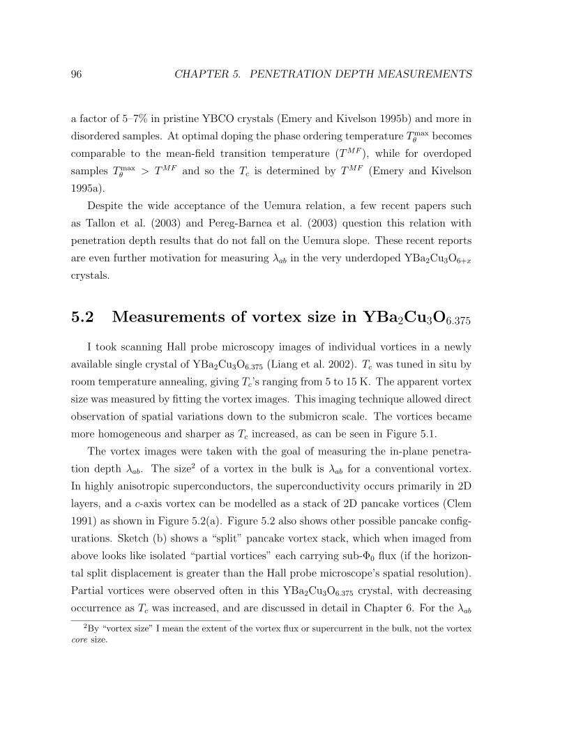
96 CHAPTER 5. PENETRATION DEPTH MEASUREMENTS
a factor of 5–7% in pristine YBCO crystals (Emery and Kivelson 1995b) and more in
disordered samples. At optimal doping the phase ordering temperature Tmaxθ becomes
comparable to the mean-field transition temperature (TMF ), while for overdoped
samples Tmaxθ > TMF and so the Tc is determined by TMF (Emery and Kivelson
1995a).
Despite the wide acceptance of the Uemura relation, a few recent papers such
as Tallon et al. (2003) and Pereg-Barnea et al. (2003) question this relation with
penetration depth results that do not fall on the Uemura slope. These recent reports
are even further motivation for measuring λab in the very underdoped YBa2Cu3O6+x
crystals.
5.2 Measurements of vortex size in YBa2Cu3O6.375
I took scanning Hall probe microscopy images of individual vortices in a newly
available single crystal of YBa2Cu3O6.375 (Liang et al. 2002). Tc was tuned in situ by
room temperature annealing, giving Tc’s ranging from 5 to 15 K. The apparent vortex
size was measured by fitting the vortex images. This imaging technique allowed direct
observation of spatial variations down to the submicron scale. The vortices became
more homogeneous and sharper as Tc increased, as can be seen in Figure 5.1.
The vortex images were taken with the goal of measuring the in-plane penetra-
tion depth λab. The size2 of a vortex in the bulk is λab for a conventional vortex.
In highly anisotropic superconductors, the superconductivity occurs primarily in 2D
layers, and a c-axis vortex can be modelled as a stack of 2D pancake vortices (Clem
1991) as shown in Figure 5.2(a). Figure 5.2 also shows other possible pancake config-
urations. Sketch (b) shows a “split” pancake vortex stack, which when imaged from
above looks like isolated “partial vortices” each carrying sub-Φ0 flux (if the horizon-
tal split displacement is greater than the Hall probe microscope’s spatial resolution).
Partial vortices were observed often in this YBa2Cu3O6.375 crystal, with decreasing
occurrence as Tc was increased, and are discussed in detail in Chapter 6. For the λab
2By “vortex size” I mean the extent of the vortex flux or supercurrent in the bulk, not the vortexcore size.
5.2. MEASUREMENTS OF VORTEX SIZE IN YBa2Cu3O6.375 97
(a)
Tc=5.1 K
Bmax
=0.47 G
(b)T
c=6.5 K
Bmax
=0.73 G
(c)T
c=8.6 K
Bmax
=1.09 G
(d)T
c=11.5 K
Bmax
=1.44 G
(e)T
c=13.1 K
Bmax
=1.62 G
(f)T
c=14.0 K
Bmax
=0.95 G
(g)
Tc=14.4 K
Bmax
=1.41 G
(h)T
c=14.7 K
Bmax
=1.59 G
10 µm
Figure 5.1: Individual vortices imaged with a 0.5 µm Hall probe in a YBa2Cu3O6.375 crystalwith variable Tc. These 42 images were each fit to a model of the vortex field profile todetermine the apparent vortex size (sab, where sab = λab if there is not staggered pinningof pancake vortices). Rows (a)–(h) show images obtained for increasing Tc values. In eachrow the images are arranged from left to right by decreasing fitted sab values. A constantoffset, determined by fitting, was subtracted from each image. The color-scale for each rowextends from −Bmax/10 (blue) to +Bmax (red). The height of the Hall probe z = z0 + ∆zwas not the same for all images, ∆z differed by a controlled amount ≤0.16 µm, though webelieve z0 was constant.
98 CHAPTER 5. PENETRATION DEPTH MEASUREMENTS
(a) (b) (c)
Figure 5.2: Possible configurations of 2D pancake vortices in a layered superconductor.(a) A straight pancake vortex stack is identical to a conventional 3D vortex in the limitof small layer spacing. (b) A split stack which looks like isolated “partial vortices” whenviewed from above. (c) A vortex with staggered pinning of the pancakes. The apparent sizeof a staggered stack is larger than that of the straight stack in (a).
measurements, I chose images of vortices which were quasi-isolated and brighter than
any nearby partial vortices, in an attempt to select full vortices described by Figure
5.2(a) rather than split stacks as in Figure 5.2(b). However, this does not exclude the
possibility of a staggered stack as sketched in Figure 5.2(c), in which the pancakes are
pinned in each layer with slight random displacements. The apparent size of a vortex
composed of staggered pancakes would be larger than λab. We cannot tell from our
images if the apparent full vortices are described by Figure 5.2(a) or (c). My vortex
fits measure the apparent vortex size, which I will denote as sab. This size is the sum
of λab and the average of the pancake displacements in the staggered stack. If there
is no staggered pinning of the 2D pancake vortices, then sab = λab.
5.2.1 The YBCO sample
It has proven difficult to make very underdoped cuprate superconductors with
sharp Tc’s. In YBCO, the doping is controlled by high mobility chain oxygens, mak-
ing it possible to achieve a high degree of homogeneity. Very underdoped high-purity
YBCO crystals are grown with a recently improved self-flux method in BaZrO3 cru-
cibles by Liang et al. (1998, 2002). The desired oxygen content is set during a 900–
930C anneal in flowing oxygen, then oxygen inhomogeneities are removed during
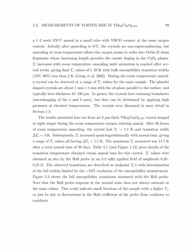
5.2. MEASUREMENTS OF VORTEX SIZE IN YBa2Cu3O6.375 99
a 1–2 week 570C anneal in a small tube with YBCO ceramic at the same oxygen
content. Initially after quenching to 0C, the crystals are non-superconducting, but
annealing at room temperature allows the oxygen atoms to order into Ortho-II chain
fragments whose increasing length provides the carrier doping in the CuO2 planes.
Tc increases with room temperature annealing until saturation is reached after sev-
eral weeks, giving final Tc values of 5–20 K with bulk susceptibility transition widths
(10%–90%) less than 2 K (Liang et al. 2002). During the room temperature anneal,
a crystal can be observed at a range of Tc values for the same sample. The platelet
shaped crystals are about 1 mm×1 mm with the ab-plane parallel to the surface, and
typically have thickness 10–100 µm. As grown, the crystals have twinning boundaries
(interchanging of the a and b axes), but they can be detwinned by applying high
pressures at elevated temperatures. The crystals were discussed in more detail in
Section 1.3.
The results presented here are from an 8 µm thick YBa2Cu3O6.375 crystal imaged
at eight stages during the room temperature oxygen ordering anneal. After 36 hours
of room temperature annealing, the crystal had Tc ∼ 5.1 K and transition width
∆Tc ∼ 3 K. Subsequently, Tc increased quasi-logarithmically with anneal time, giving
a range of Tc values all having ∆Tc < 1.5 K. The maximum Tc measured was 14.7 K
after a total anneal time of 39 days. Table 5.1 (and Figure 1.13) gives details of the
transition temperature obtained versus anneal time for this crystal. Tc values were
obtained in situ by the Hall probe in an 8.3 mHz applied field of amplitude 0.20–
0.25 G. The observed transitions are described as midpoint Tc’s with determination
of the full widths limited by the ∼10% resolution of the susceptibility measurement.
Figure 5.3 shows the full susceptibility transitions measured with the Hall probe.
Note that the Hall probe response in the normal state does not always saturate at
the same values. This could indicate small fractions of the sample with a higher Tc,
or just be due to fluctuations in the Hall coefficient of the probe from cooldown to
cooldown.
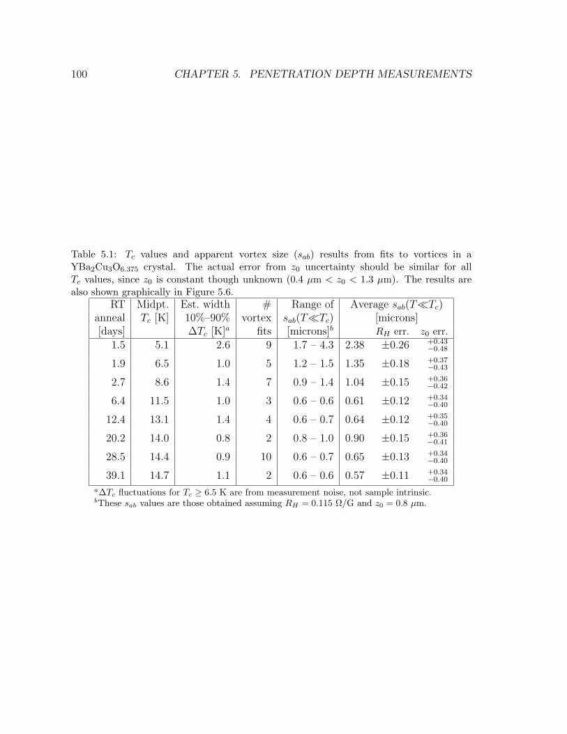
100 CHAPTER 5. PENETRATION DEPTH MEASUREMENTS
Table 5.1: Tc values and apparent vortex size (sab) results from fits to vortices in aYBa2Cu3O6.375 crystal. The actual error from z0 uncertainty should be similar for allTc values, since z0 is constant though unknown (0.4 µm < z0 < 1.3 µm). The results arealso shown graphically in Figure 5.6.
RT Midpt. Est. width # Range of Average sab(T¿Tc)anneal Tc [K] 10%–90% vortex sab(T¿Tc) [microns][days] ∆Tc [K]a fits [microns]b RH err. z0 err.
1.5 5.1 2.6 9 1.7 – 4.3 2.38 ±0.26 +0.43−0.48
1.9 6.5 1.0 5 1.2 – 1.5 1.35 ±0.18 +0.37−0.43
2.7 8.6 1.4 7 0.9 – 1.4 1.04 ±0.15 +0.36−0.42
6.4 11.5 1.0 3 0.6 – 0.6 0.61 ±0.12 +0.34−0.40
12.4 13.1 1.4 4 0.6 – 0.7 0.64 ±0.12 +0.35−0.40
20.2 14.0 0.8 2 0.8 – 1.0 0.90 ±0.15 +0.36−0.41
28.5 14.4 0.9 10 0.6 – 0.7 0.65 ±0.13 +0.34−0.40
39.1 14.7 1.1 2 0.6 – 0.6 0.57 ±0.11 +0.34−0.40
a∆Tc fluctuations for Tc ≥ 6.5 K are from measurement noise, not sample intrinsic.bThese sab values are those obtained assuming RH = 0.115 Ω/G and z0 = 0.8 µm.
5.2. MEASUREMENTS OF VORTEX SIZE IN YBa2Cu3O6.375 101
2 4 6 8 10 12 14 16 18−0.03
0
0.03
0.06
0.09
0.12
0.15
Temperature (K)
Hal
l Res
pons
e (Ω
/G)
Figure 5.3: Superconducting transitions in the YBa2Cu3O6.375 crystal as measured by insitu magnetic susceptibility. Each color represents a different anneal stage. Triangles arefor second measurements. Vertical lines indicate the estimated midpoint Tc of the full widthtransition at each anneal stage. The data for the two lowest Tc’s (red and orange) werewith Bmax = 0.25 G, except for the red * data points which were with Bmax = 1.0 G. Allhigher Tc transitions were taken with Bmax = 0.20 G. The Hall coefficient was estimatedto be RH = 0.115± 0.015 Ω/G.
102 CHAPTER 5. PENETRATION DEPTH MEASUREMENTS
5.2.2 Vortex imaging
Scanning Hall probe microscopy of single vortices is an established technique
(Chang et al. 1992; Davidovic et al. 1996; Oral et al. 1996b) first demonstrated by
Chang et al. (1992). The Hall probe used here was made from GaAs/AlGaAs two-
dimensional electron gas (2DEG) and had lithographic size 0.5 µm × 0.5 µm. (See
Section 3.4). Due to depletion in the 2DEG, the size of the active area is somewhat
smaller than the lithographic dimensions. The Hall probe measures the perpendicu-
lar magnetic field in the active area, with respect to a constant offset intrinsic to the
probe. The minimum height z0 of the active area above the sample surface is limited
by the 2DEG depth (140 nm), by the distance between the active area and the corner
of the Hall probe chip (8 µm), and by the angle between the Hall probe chip and the
sample (≥1). z0 is determined by precise alignment and is by far the largest source
of error in my fit results. For this reason it was critical to make measurements for a
range of Tc on the same crystal during a single alignment to keep z0 constant and
thus control the systematic error. I performed the room temperature annealing of
the YBa2Cu3O6.375 sample in situ to keep z0 constant.
Isolated vortices were trapped by cooling the sample in a small applied field inside
triple-layer mu-metal magnetic shielding with a residual field <25 mG. Figures 5.1
shows vortex images for the range of Tc values. At lower Tc the vortex fields are more
spread out and have smaller amplitude, indicative of a larger apparent size sab. The
lower Tc vortices were often non-circular, particularly for the minimum Tc = 5.1 K,
and also showed more variation in peak height from vortex to vortex. In general, the
vortices at higher Tc looked sharper and more uniform. It should be mentioned that
the asymmetries of the vortex shapes were not consistently aligned with the ab axes,
and thus are not a result of differences between λa and λb. If that were the case,
and if our crystal had been detwinned (it was not), this Hall probe technique could
in principle independently measure the two components of the in-plane penetration
depth.
The apparent vortex size sab in the bulk is related to the degree of spreading of the
vortex field profile above the sample surface. As mentioned earlier, there could be two
contributions to the apparent size sab measured in this very underdoped anisotropic
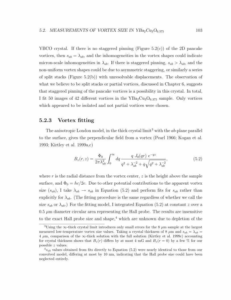
5.2. MEASUREMENTS OF VORTEX SIZE IN YBa2Cu3O6.375 103
YBCO crystal. If there is no staggered pinning (Figure 5.2(c)) of the 2D pancake
vortices, then sab = λab, and the inhomogeneities in the vortex shapes could indicate
micron-scale inhomogeneities in λab. If there is staggered pinning, sab > λab, and the
non-uniform vortex shapes could be due to asymmetric staggering, or similarly a series
of split stacks (Figure 5.2(b)) with unresolvable displacements. The observation of
what we believe to be split stacks or partial vortices, discussed in Chapter 6, suggests
that staggered pinning of the pancake vortices is a possibility in this crystal. In total,
I fit 50 images of 42 different vortices in the YBa2Cu3O6.375 sample. Only vortices
which appeared to be isolated and not partial vortices were chosen.
5.2.3 Vortex fitting
The anisotropic London model, in the thick crystal limit3 with the ab-plane parallel
to the surface, gives the perpendicular field from a vortex (Pearl 1966; Kogan et al.
1993; Kirtley et al. 1999a,c)
Bz(r, z) =Φ0
2πλ2ab
∫ ∞
0
dqq J0(qr) e−qz
q2 + λ−2ab + q
√q2 + λ−2
ab
, (5.2)
where r is the radial distance from the vortex center, z is the height above the sample
surface, and Φ0 = hc/2e. Due to other potential contributions to the apparent vortex
size (sab), I take λab → sab in Equation (5.2) and perform fits for sab rather than
explicitly for λab. (The fitting procedure is the same regardless of whether we call the
size sab or λab.) For the fitting model, I integrated Equation (5.2) at constant z over a
0.5 µm diameter circular area representing the Hall probe. The results are insensitive
to the exact Hall probe size and shape,4 which are unknown due to depletion of the
3Using the ∞-thick crystal limit introduces only small errors for the 8 µm sample at the largestmeasured low-temperature vortex size values. Taking a crystal thickness of 8 µm and sab = λab =4 µm, comparison of the ∞-thick solution with the full solution (Kirtley et al. 1999c) accountingfor crystal thickness shows that Bz(r) differs by at most 4 mG and Bz(r = 0) by a few % for ourpossible z values.
4sab values obtained from fits directly to Equation (5.2) were nearly identical to those from ourconvolved model, differing at most by 10 nm, indicating that the Hall probe size could have beenneglected entirely.
104 CHAPTER 5. PENETRATION DEPTH MEASUREMENTS
2DEG. I fit the vortex images using non-linear regression with Mathematica r© to
extract sab with fixed z. Free parameters were the location of the vortex center, a
constant offset, and sab. See Appendix A for further details on the model and fitting
procedure. The lengths z and sab are strongly correlated and could not both be free
parameters.
In the scanning microscope z = z0 + ∆z, where z0 is the sample-probe distance
when touching, and ∆z is controllable and for these measurements ranged from 0–
0.16 µm. A lower bound of z0 ≥ 0.4 µm exists from geometric constraints. A very
conservative upper bound of z0 ≤ 1.45 µm was obtained for this data set by fitting
the vortices at maximum Tc with sab = λab = 0 and z as a free parameter (see
Section A.1). A smaller upper bound of z0 ≤ 1.3 µm was obtained by assuming that
sab(0) is at least as large as λab(0) values measured in optimally doped YBCO (Basov
et al. 1995). This is still a conservative assumption, since it is well known that the
superfluid density decreases (and thus the penetration depth increases) as doping is
reduced from optimal. All vortices were fit with a range of z0 values. Fit results are
reported here with a typical value z0 = 0.8 µm, with systematic error bars determined
by fits with z0 = 0.4 µm and z0 = 1.3 µm. The choice of the typical z0 value was
based on earlier alignments and measurements of vortices in samples with known λab.
I also imaged other very underdoped YBCO crystals at single Tc values, three
with a 0.5 µm Hall probe and others with larger sensors, and obtained consistent sab
results. Fits to vortices in a second YBa2Cu3O6.375 crystal (50 µm thick) measured at
Tc = 8.3 K gave sab = 1.0–1.1 µm with the choice of z0 = 0.8 µm. Two YBa2Cu3O6.358
crystals were also imaged at their saturation Tc = 17 K. Vortices in these samples
gave sab ranging from 1.3–2.1 µm with the choice of z0 = 0.8 µm. However, these
choices of z0 for the fits were arbitrary and not experimentally verifiable. Roughly,
error in z0 translates to the same magnitude and opposite sign of error in sab, since
the parameters are highly correlated. The measurements in these three crystals had
uncontrolled systematic errors, primarily the uncertainty in z0 which was bounded
only by z0 > 0.4 µm, so in this chapter I focus on data obtained from the single sample
of YBa2Cu3O6.375 over a range of Tc, which allowed partial control of the systematic
z error.
5.2. MEASUREMENTS OF VORTEX SIZE IN YBa2Cu3O6.375 105
I did make attempts to measure the angle between the sample and the probe, which
would in principle allow calculation of the minimum height z0 of the probe active area
above the sample. This was done with a CCD camera and microscope which could
view the sample-probe alignment through the side optical ports of the cryostat. This
method of determining z0 did not give trustworthy results. For example, I imaged
vortices in a near-optimally doped YBCO crystal, for which λab has been measured
by other techniques in similar samples. The anisotropy of optimally doped YBCO is
much lower than for the very underdoped crystals, so the observed apparent vortex
size sab should equal λab in the near-optimally doped crystal. During one alignment,
fits to the vortices in that sample with z as a free parameter gave z0 = 2.1 µm (a
larger than usual value), while measurement of the sample-probe angle obtained with
the camera predicted only z0 ≈ 0.7 µm. The z discrepancies could be due to curvature
of the sample, inability to measure the angle accurately from the optical pictures, or
even due to extra material on the tip or sample surface which would contribute extra
distance to z0. In light of these problems, I conservatively state the errors in the sab
results without attempting to measure z0 from the alignment angle.
In another attempt to tighten the uncertainty limits of z0, I performed many fits
to three vortices in the YBa2Cu3O6.375 crystal at the Tc = 8.6 K anneal stage. The
fits were done for a large array of fixed z and sab values to see how the goodness of
fit depended on those parameters. (For these vortex images ∆z was zero, so z = z0.)
The lower the Tc, the larger the sab, and thus the further away we are from the
limit in which Equation (5.2) (with λab → sab) simplifies to a monopole solution
(Appendix A.1) where z and sab enter only as (z + sab). I did not choose vortices
with Tc < 8.6 K, which had even larger apparent vortex size sab, since they were less
homogeneous and thus not as ideal for fitting. I computed the average squared error
between the data and fits for a grid of z and sab. Selecting only those fits within a 90%
confidence interval gave z ranges of 0.1− 0.6, 0.3− 1.1, and 0.1− 0.3 µm respectively
for the three vortices. Clearly this is not a sufficient method to place bounds on
z0, since the 90% limits placed by each vortex do not even all overlap, and values
z0 < 0.4 µm are not physically possible due to geometric constraints. Furthermore,
this analysis assumed a normal distribution of errors, which is not the actual case and
106 CHAPTER 5. PENETRATION DEPTH MEASUREMENTS
which underestimates the z spread of the confidence intervals. This analysis further
confirmed that z and sab are just too correlated to treat them independently. A new
scheme to accurately determine z0 is highly desirable, such as a probe fabricated with
a small STM pillar on top of the active area. Then z0 would be equal to the pillar
height plus the depth of the 2DEG.
5.2.4 Results
Figure 5.4 shows 2D fits of representative vortices at low temperature for the
lowest and highest Tc values of 5.1 and 14.7 K. Fitting the radially symmetric model
to inhomogeneous vortex profiles such as Figure 5.4(a) is an approximation which
gives an average of the apparent vortex size.
For four vortices I also took Hall probe images while warming to investigate tem-
perature dependence. Figure 5.5(a) plots the apparent vortex size sab(T ) for vortices
at the minimum and maximum Tc stages. The superfluid density (∝ λ−2ab ) in cuprates
has been found experimentally to be linear in T for T ¿ Tc (Hardy et al. 1993). This
slope d(λ−2ab )/dT has also been found to be doping independent (Bonn et al. 1996).
Within our systematic and statistical errors, it is not possible to extract the details of
the temperature dependence of the penetration depth (if we assume sab = λab) from
our measurements. Figure 5.5(b) plots s−2ab (T ) for our data along with λ−2
a (T ) data
for YBa2Cu3O6.60 from (Bonn et al. 1996) for comparison. The slopes of our data
are consistent with the YBa2Cu3O6.60 data, but meaningful conclusions cannot be
drawn due to our large systematic error bars. The measured sab is roughly constant
for T . Tc/2 (Figure 5.5(a)). Thus I approximate sab(0) by sab(T ) with T ∼ 2 K for
Tc < 12 K and T ∼ 4 K for higher Tc’s.
The low temperature apparent vortex size sab versus Tc results are shown in Figure
5.6(a) and summarized in Table 5.1. The apparent vortex size is an upper bound on
λab, and if there is not broadening due to pinning, sab = λab. To check the robustness
of the fit to the amount of included background, for six vortices I took multiple images
varying only the image size. The sab values varied by at most 0.1 µm and I averaged
these sab results to obtain one data point per vortex. The dominant sources of error
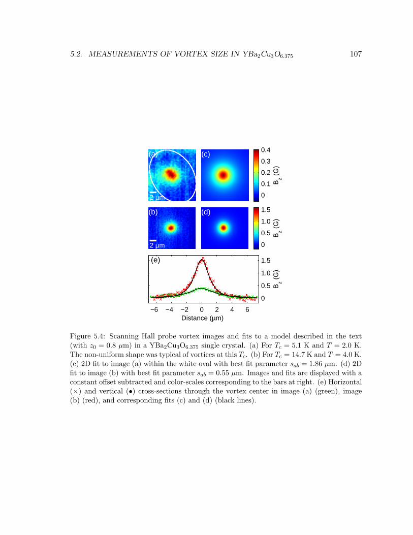
5.2. MEASUREMENTS OF VORTEX SIZE IN YBa2Cu3O6.375 107
(a)
2 µm 0
0.1
0.2
0.3
0.4(c)
(b)
2 µm 0
0.5
1.0
1.5(d)
Bz (
G)
Bz (
G)
−6 −4 −2 0 2 4 6
0
0.5
1.0
1.5
Distance (µm)
(e)
Bz (
G)
Figure 5.4: Scanning Hall probe vortex images and fits to a model described in the text(with z0 = 0.8 µm) in a YBa2Cu3O6.375 single crystal. (a) For Tc = 5.1 K and T = 2.0 K.The non-uniform shape was typical of vortices at this Tc. (b) For Tc = 14.7 K and T = 4.0 K.(c) 2D fit to image (a) within the white oval with best fit parameter sab = 1.86 µm. (d) 2Dfit to image (b) with best fit parameter sab = 0.55 µm. Images and fits are displayed with aconstant offset subtracted and color-scales corresponding to the bars at right. (e) Horizontal(×) and vertical (•) cross-sections through the vortex center in image (a) (green), image(b) (red), and corresponding fits (c) and (d) (black lines).
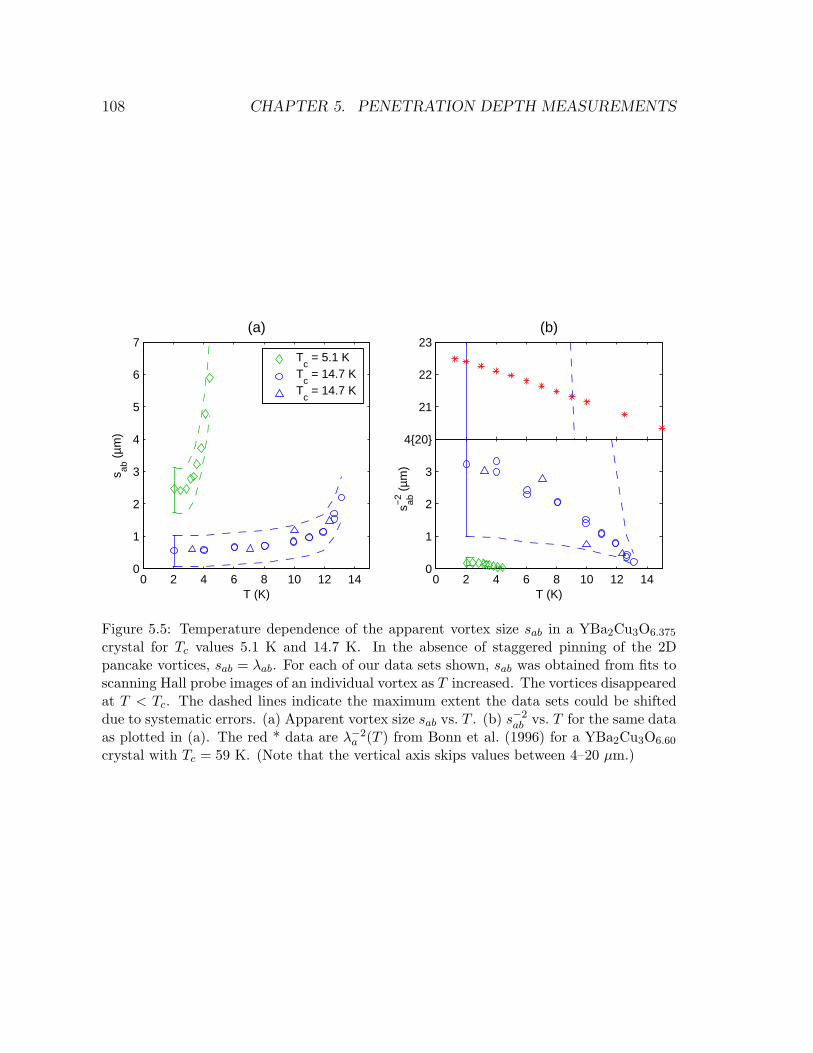
108 CHAPTER 5. PENETRATION DEPTH MEASUREMENTS
0 2 4 6 8 10 12 140
1
2
3
4
5
6
7
T (K)
s ab (
µm)
(a)
Tc = 5.1 K
Tc = 14.7 K
Tc = 14.7 K
21
22
23
T (K)
(b)
0 2 4 6 8 10 12 140
1
2
3
420
T (K)
s ab−2 (
µm)
Figure 5.5: Temperature dependence of the apparent vortex size sab in a YBa2Cu3O6.375
crystal for Tc values 5.1 K and 14.7 K. In the absence of staggered pinning of the 2Dpancake vortices, sab = λab. For each of our data sets shown, sab was obtained from fits toscanning Hall probe images of an individual vortex as T increased. The vortices disappearedat T < Tc. The dashed lines indicate the maximum extent the data sets could be shifteddue to systematic errors. (a) Apparent vortex size sab vs. T . (b) s−2
ab vs. T for the same dataas plotted in (a). The red * data are λ−2
a (T ) from Bonn et al. (1996) for a YBa2Cu3O6.60
crystal with Tc = 59 K. (Note that the vertical axis skips values between 4–20 µm.)
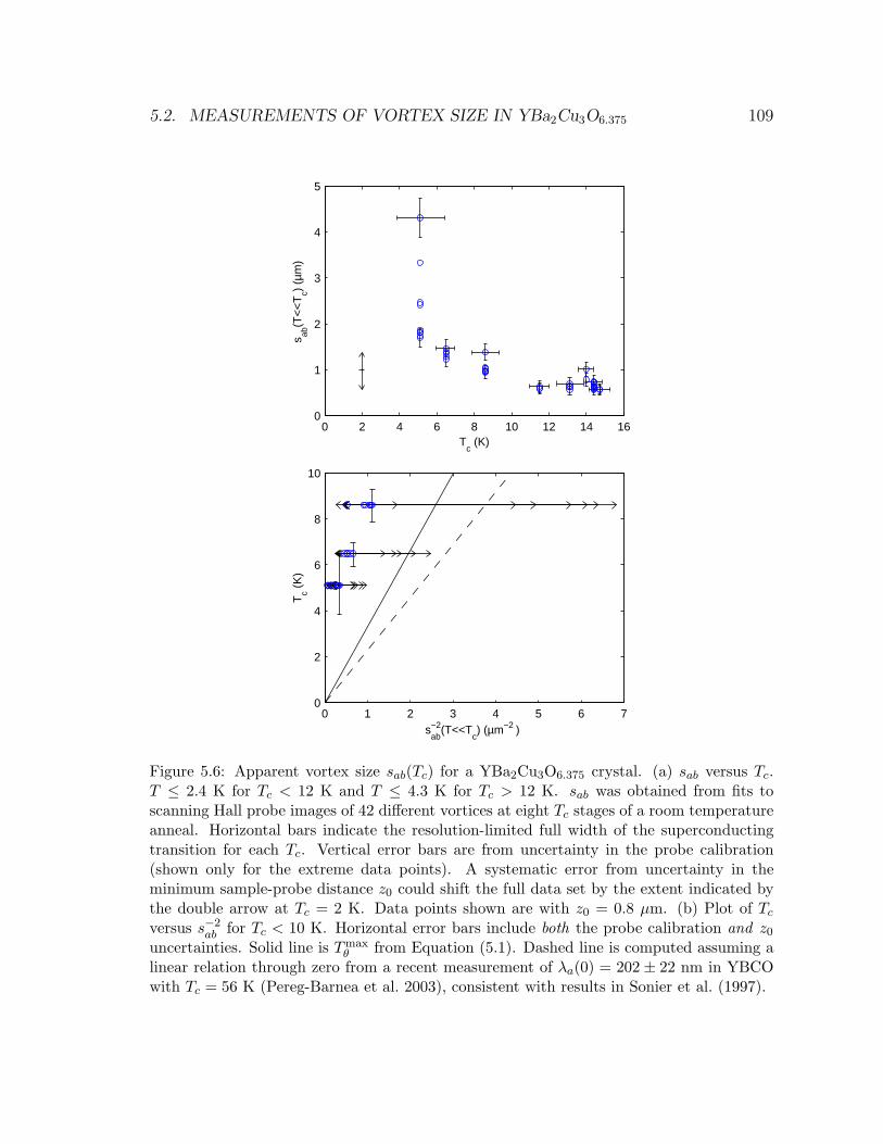
5.2. MEASUREMENTS OF VORTEX SIZE IN YBa2Cu3O6.375 109
0 2 4 6 8 10 12 14 160
1
2
3
4
5
Tc (K)
s ab(T
<<
Tc)
(µm
)
0 1 2 3 4 5 6 70
2
4
6
8
10
sab−2(T<<T
c) (µm−2 )
Tc (
K)
Figure 5.6: Apparent vortex size sab(Tc) for a YBa2Cu3O6.375 crystal. (a) sab versus Tc.T ≤ 2.4 K for Tc < 12 K and T ≤ 4.3 K for Tc > 12 K. sab was obtained from fits toscanning Hall probe images of 42 different vortices at eight Tc stages of a room temperatureanneal. Horizontal bars indicate the resolution-limited full width of the superconductingtransition for each Tc. Vertical error bars are from uncertainty in the probe calibration(shown only for the extreme data points). A systematic error from uncertainty in theminimum sample-probe distance z0 could shift the full data set by the extent indicated bythe double arrow at Tc = 2 K. Data points shown are with z0 = 0.8 µm. (b) Plot of Tc
versus s−2ab for Tc < 10 K. Horizontal error bars include both the probe calibration and z0
uncertainties. Solid line is Tmaxθ from Equation (5.1). Dashed line is computed assuming a
linear relation through zero from a recent measurement of λa(0) = 202± 22 nm in YBCOwith Tc = 56 K (Pereg-Barnea et al. 2003), consistent with results in Sonier et al. (1997).
110 CHAPTER 5. PENETRATION DEPTH MEASUREMENTS
in the sab results are the uncertainty in z0 (which will be the same for all data points)
and the calibration of the probe’s Hall coefficient, RH = 0.115±0.015 Ω/G. Fits with
the z0 extremes show that the corresponding sab error, indicated by the double arrow
in Figure 5.6(a) and given for the average sab(Tc) in Table 5.1, is roughly constant for
all data points. The uncertainty in RH translates to an sab error of roughly ±8% of
(z + sab). RH can change slightly from cooldown to cooldown, so unlike z0, it is not
necessarily the same for all the Tc values. Under the assumption that Equation (5.2)
with λab → sab is the correct theoretical description of our measured field profiles,
other systematic and statistical errors are small compared to those of z0 and RH .
At the lowest Tc of 5.1 K, the apparent vortex size sab varies significantly from
vortex to vortex and ∆Tc is nearly twice that of higher Tc’s. This might be explained
by local Tc variations on the tens-of-micron length scale and could suggest that the
oxygen ordering and in-plane doping was somewhat inhomogeneous after the shortest
anneal time. The narrow widths ∆Tc < 1.5 K and smaller sab variations for Tc ≥6.5 K may indicate increased homogeneity. Alternatively, sab might be dominated
by staggered pinning of the pancake vortices (Figure 5.2(c)) at the lowest Tc’s, or
undetected split pancake stacks, and thus the variations in sab could be due to pinning.
It is useful to examine the sab results in the assumed case of sab = λab. Figure
5.6(b) shows the low temperature data plotted as Tc versus s−2ab (recall that λ−2
ab is
proportional to the superfluid density). The data deviate from the linear Uemura re-
lation, shown as the solid line. The fits gave low temperature values sab ≈ 1.7−4.3 µm
for the lowest Tc ∼ 5 K. In contrast, Equation (5.1) gives Tc ≈ (3.3 K µm2)λ−2ab (0)
for YBCO, or λab(0) = 0.8 µm for Tc = 5 K. If sab = λab, then my data indicate that
a smaller ns(0) can yield 5 and 6.5 K transition temperatures. The higher Tc data
are inconclusive due to increasingly large error bars from the z0 uncertainty. If the
Uemura line is computed from a recent measurement of λa(0) by Pereg-Barnea et al.
(2003), as shown by the dashed line in Figure 5.6(b), our data deviate even more
from the line.
5.2. MEASUREMENTS OF VORTEX SIZE IN YBa2Cu3O6.375 111
5.2.5 Discussion and implications
The interpretation of my apparent vortex size measurements as a function of Tc in
the very underdoped YBa2Cu3O6+x is contingent on the behavior of the 2D pancake
vortices schematically shown in Figure 5.2. If the imaged vortices were not straight
pancake stacks, but instead pinned with unresolvable horizontal displacements, the
apparent vortex size sab would be larger than λab.
Let us examine the pancake vortices in more detail. These crystals have a large
anisotropy λc/λab, as confirmed by recent measurements of λc(0) ∼ 100 µm for Tc ∼6 K (Hosseini et al. 2003), so it is indeed appropriate to treat a vortex as composed
of 2D pancake vortices as first introduced by Clem (1991). Neglecting Josephson
coupling (λc →∞), the potential of a single pancake dislocated a distance ρ from an
otherwise straight stack is (Clem 1991):
U0(ρ) = E0[γ + ln(ρ/2λab) + K0(ρ/λab)], (5.3)
where E0 = Φ20s/(8π
2λ2ab), γ is Euler’s constant, and s = 1.17 nm is the YBCO bilayer
spacing. Assuming λab = 0.8 µm from Equation (5.1) at Tc = 5 K, the potential well
width would be ρ < 0.3 µm for U0(ρ)/kB < 5 K. This indicates that pancake thermal
fluctuations cannot be the sole source of our large apparent vortex sizes. Bluhm
confirmed this calculation with Monte Carlo simulations of the whole pancake stack
using the exact magnetic interaction potential including surface effects.
As mentioned already, pinning might cause misalignment of the pancakes. The
force required to unpin a vortex has been estimated by Gardner et al. (2002) to be
∼0.5 pN for a similar YBCO crystal with Tc = 11 K. This is the total force on roughly
a thousand pancakes within a penetration depth of the surface. The restoring force
on a dislocated pancake calculated from U0(ρ) is of order 0.5 fN, showing that pinning
could be strong enough to distort the straight pancake stack, resulting in a staggered
pancake stack (shown in Figure 5.2(c)). Thorough studies of pinning landscapes in
these and other cuprates are needed.
If pinning turns out not to be contributing to our measured apparent vortex size
sab, then sab = λab, and the data indicate that the model of a linear upper bound
112 CHAPTER 5. PENETRATION DEPTH MEASUREMENTS
on Tc due to phase fluctuations in a quasi-2D superconductor, Equation (5.1) with
a = d > ξc, is not appropriate here. Within the context of Equation (5.1), other length
scales could determine a. ξc has not been measured in these samples and could be
larger than d, as would be expected if the disappearance of superconductivity at low
doping is described by a quantum critical point. If there is a continuous T = 0
superconducting to non-superconducting transition at a critical doping level x0, the
coherence length ξ (and ξc) must diverge as x → x0. There would be a crossover to
3D physics with ξc À d, and thus at very low doping ξc would be the characteristic
length scale a, yielding Tc ∝ ξcλ−2ab (0) (Kivelson). Alternatively, if the superconductor
is granular and undergoes a percolation transition as doping decreases, a could be
determined by the cluster size (Kivelson). Either scenario is qualitatively consistent
with our data. The noticeably inhomogeneous field profiles in the lowest Tc data may
support the idea of an inhomogeneous superconductor at the micron scale, but give
no direct information on granularity at the nanometer or tens of nanometers scale.
5.3 Conclusions
In summary, I used a scanning Hall probe microscope to image individual vortices
in very underdoped YBa2Cu3O6+x with Tc varied from 5 to 15 K. I observed spatial
variations of the vortex field profiles at the lowest Tc’s and from fits obtained the
apparent vortex size sab(Tc). If this size is governed only by λab(Tc), the results
do not agree with the widely accepted Uemura relation Tc ∝ λ(0)−2 ∝ ns(0)/m∗.
Instead, they would indicate that lower superfluid densities can support Tc’s of 5.1
and 6.5 K. Note that this deviation cannot be explained by including quantum phase
fluctuations (Emery and Kivelson 1995a,b) because that would predict deviations in
the other direction (higher ns/m∗ for these Tc values).
The alternative explanation for the large apparent vortex sizes is that the vortices
are not appropriately modelled as a straight stack of pancake vortices, but are instead
pinned as misaligned or “staggered” stacks. In that case our measurements of the
apparent vortex size sab are a superposition of the in-plane penetration depth and the
length scale of the pancake displacements. Our results do yield upper bounds on λab,
5.3. CONCLUSIONS 113
since λab ≤ sab.
The very underdoped region of the cuprate phase diagram is important to study,
and is available for experiment thanks to the YBCO single crystals from UBC (Liang
et al. 1998, 2002). Other techniques for measuring λab should be performed on these
very underdoped crystals to supplement the results presented here. The recent results
presented by Pereg-Barnea et al. (2003) and Tallon et al. (2003) show deviations from
the linear Uemura relation for higher dopings than our very underdoped crystals.
More sample development and studies of other very underdoped cuprates will help
determine the underlying physics in these samples.
114 CHAPTER 5. PENETRATION DEPTH MEASUREMENTS
Chapter 6
Partial vortices
In this chapter I will discuss unexpected observations of magnetic vortices which
appeared to carry total flux less than the superconducting flux quantum Φ0 = hc/2e.
These features were observed with scanning magnetic microscopy in very underdoped
YBa2Cu3O6+x (YBCO) single crystals with x ≈ 0.35 − 0.375. (See Section 1.3 for a
basic introduction to the crystals.) Observations were made initially with an 8 µm
Superconducting QUantum Interference Device (SQUID) and later more extensively
with a 0.5 µm Hall probe.
Fluxoid quantization is a fundamental property of superconductivity. For this
reason it was surprising to see these apparent isolated sub-Φ0 features, which I will
call partial vortices. In this Chapter I will first briefly review fluxoid quantization in
a superconductor. In Section 6.2 I will introduce the partial vortex images, discuss
properties of the partial vortices, and give statistics on their prevalence and magni-
tude. Then I will discuss some of the initial but rejected scenarios for creating these
partial vortices before introducing a proposal for what these partial vortices really are.
We believe they are caused by a full vortex that is partially displaced horizontally
(a “split pancake vortex stack”). This is possible only in quasi-2D layered super-
conductors where the vortex can be treated as stack of 2D pancake vortices (Clem
1991). Flux quantization is not violated by the split stack. In Section 6.4 I discuss
the split stack idea in detail and show that it does indeed agree with experimental
observations.
115
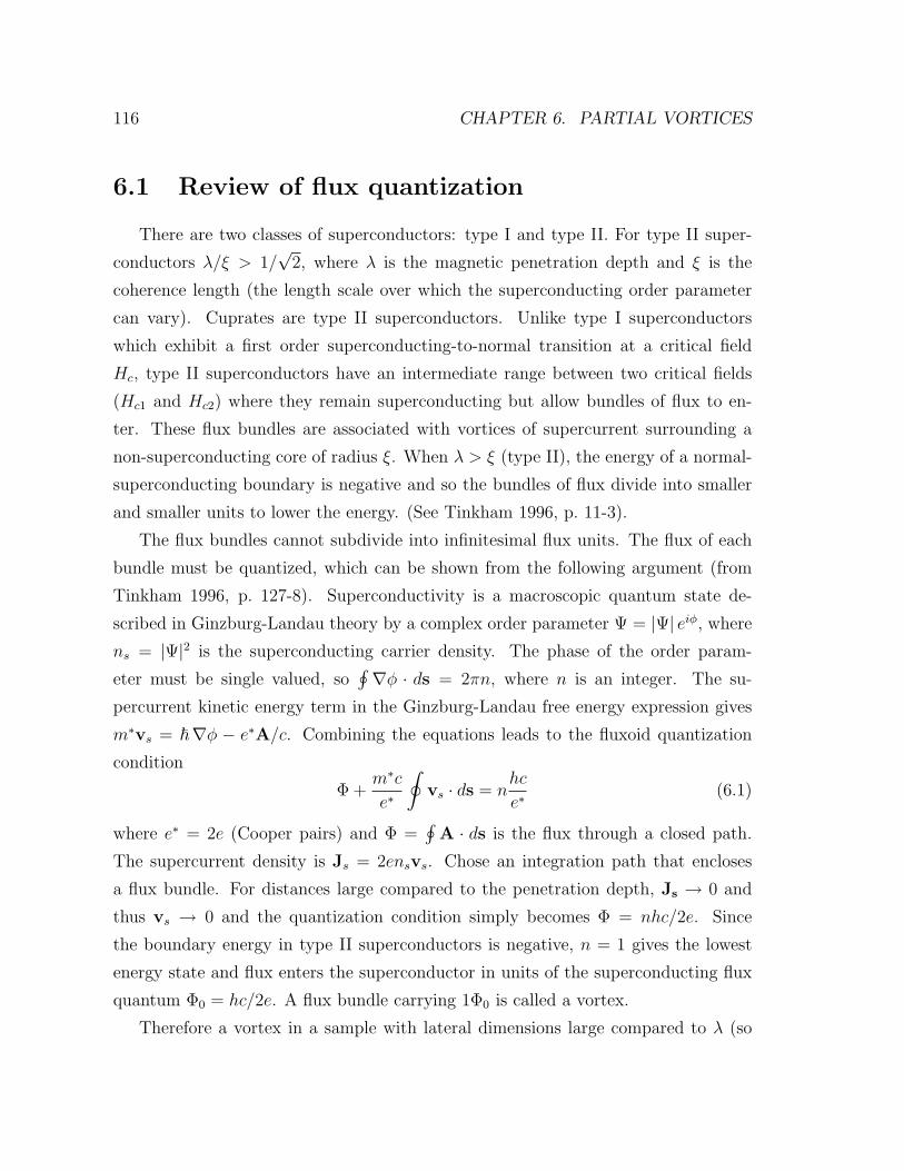
116 CHAPTER 6. PARTIAL VORTICES
6.1 Review of flux quantization
There are two classes of superconductors: type I and type II. For type II super-
conductors λ/ξ > 1/√
2, where λ is the magnetic penetration depth and ξ is the
coherence length (the length scale over which the superconducting order parameter
can vary). Cuprates are type II superconductors. Unlike type I superconductors
which exhibit a first order superconducting-to-normal transition at a critical field
Hc, type II superconductors have an intermediate range between two critical fields
(Hc1 and Hc2) where they remain superconducting but allow bundles of flux to en-
ter. These flux bundles are associated with vortices of supercurrent surrounding a
non-superconducting core of radius ξ. When λ > ξ (type II), the energy of a normal-
superconducting boundary is negative and so the bundles of flux divide into smaller
and smaller units to lower the energy. (See Tinkham 1996, p. 11-3).
The flux bundles cannot subdivide into infinitesimal flux units. The flux of each
bundle must be quantized, which can be shown from the following argument (from
Tinkham 1996, p. 127-8). Superconductivity is a macroscopic quantum state de-
scribed in Ginzburg-Landau theory by a complex order parameter Ψ = |Ψ| eiφ, where
ns = |Ψ|2 is the superconducting carrier density. The phase of the order param-
eter must be single valued, so∮ ∇φ · ds = 2πn, where n is an integer. The su-
percurrent kinetic energy term in the Ginzburg-Landau free energy expression gives
m∗vs = ~∇φ − e∗A/c. Combining the equations leads to the fluxoid quantization
condition
Φ +m∗ce∗
∮vs · ds = n
hc
e∗(6.1)
where e∗ = 2e (Cooper pairs) and Φ =∮
A · ds is the flux through a closed path.
The supercurrent density is Js = 2ensvs. Chose an integration path that encloses
a flux bundle. For distances large compared to the penetration depth, Js → 0 and
thus vs → 0 and the quantization condition simply becomes Φ = nhc/2e. Since
the boundary energy in type II superconductors is negative, n = 1 gives the lowest
energy state and flux enters the superconductor in units of the superconducting flux
quantum Φ0 = hc/2e. A flux bundle carrying 1Φ0 is called a vortex.
Therefore a vortex in a sample with lateral dimensions large compared to λ (so
6.2. PARTIAL VORTEX OBSERVATIONS 117
that there is a path with vs = 0) cannot carry less than Φ0 of flux, because the
phase would not be single valued. There are exceptions to this statement in situa-
tions where something other than flux contributes to the phase winding. An elegant
example is the tri-crystal experiments by Kirtley et al. (1996, 1999b) which proved
that the superconducting order parameter for cuprates is d-wave (rather than s-wave
like conventional superconductors). Their experiment was done on a thick film of
YBCO specially grown in three sections, each with a different orientation of the ab
axes. The sections met at a single tri-crystal point. The crystal axes orientations and
the boundary angles were chosen to create a π phase winding around the tri-crystal
point. This is possible with a d-wave material because the order parameter has four
lobes of alternating sign. Crossing a boundary from a minus lobe to a plus lobe re-
sults in a π phase shift. Since there is already a π-shift, the flux at that point must
be half-integer to ensure that the total phase winding is 2πn. The observation by
Kirtley et al. (1996, 1999b) of a spontaneously generated half-integer flux quantum
at the tri-crystal point gave conclusive evidence for d-wave superconductivity.
The tri-crystal example shows that the presence of grain boundaries of particular
orientation in a d-wave superconductor can result in vortices of half-integer multiples
of Φ0 without violating the single-valuedness of Ψ. However in a single crystal, like
the YBa2Cu3O6+x discussed in this dissertation, there should not be grain boundaries
aside from twinning (the interchange of the a and b axes) which cannot result in any
phase winding of π or any fraction thereof. A π shift can occur across a twin boundary,
but any closed path crossing a twin boundary would have to cross an even number of
boundaries, and thus only could acquire phase windings of 2πn.
Two categories of explanations for sub-Φ0 vortices come out of the above discus-
sion: fluxoid quantization where the current does not go to zero, so Φ < Φ0, and
non-flux sources of a phase winding other than 2π.
6.2 Partial vortex observations
Partial vortices were observed in four very underdoped YBa2Cu3O6+x single crys-
tals, out of at least ten that were imaged. Generally, partial vortices were seen for
118 CHAPTER 6. PARTIAL VORTICES
Tc ∼ 7 K and not for Tc ≥ 11 K.1 Initial partial vortex observations were made with
scanning SQUID microscopy in three crystals, while more detailed studies of partial
vortices were done later on a fourth crystal with a scanning Hall probe. This crystal
had x = 0.375 and its Tc was varied in stages from 5 to 15 K by room temperature
annealing. Vortex imaging was also done on Ortho-II (Tc ≈ 60 K) and near-optimally
doped YBCO crystals, neither of which showed partial vortices.
An 8 µm scanning SQUID was used in the first observations of partial vortices
in single crystal samples of YBa2Cu3O6.354 and similar oxygen content. At least
six bulk crystals were observed with the SQUID and partial vortices were seen in
three of them. The crystals in which partial vortices were not seen had Tc between
11 and 13 K. Partial vortices were only seen with the SQUID in crystals with lower
transition temperatures obtained by annealing the samples (separately) for about one
week at ∼40C. Two of the three partial vortex SQUID samples had Tc ≈ 7 K, while
the third had an unmeasured2 Tc between 7 and 12 K. Transition widths were not
determined for all the samples, but when measured, the higher Tc samples (11–13 K)
had ∆Tc < 2 K while those with lower Tc had widths ∼3 K.
In one of the Tc ≈ 7 K samples, approximately 16 different partial vortices were
observed, as well as roughly equivalent numbers of full vortices. Some vortices were
difficult to classify due to the limited spatial resolution of the SQUID. This crystal
was also used for vortex pushing and annihilation experiments described in Gardner
et al. (2002). Two images of partial vortices in this crystal are shown in Figure 6.1.
Image (a) shows a full vortex with a partial vortex neighbor whose peak flux ΦS
through the SQUID is only ∼40% of the peak ΦS of the full vortex. The bright
vortex was determined to be a full vortex from a 1D fit using the monopole model of
a vortex field profile (see Appendix A.1). Image (b) shows two neighboring partial
vortices of different amplitude. The brighter partial vortex has twice the amplitude of
1One exception was the crystal studied at a range of Tc with the Hall probe. Partial vorticeswere observed above 11 K, but with decreasing percentages as Tc increased to 15 K.
2Transition temperatures above 7 K cannot be measured directly with the SQUID due to the NbSQUID’s low operating temperatures. For higher Tc samples studied with the SQUID, the Tc wasmeasured either in a bulk SQUID magnetometer, with a non-scanning Hall probe setup, or deducedapproximately from changes to the vortex configuration when the sample was cycled to temperaturesabove Tc.
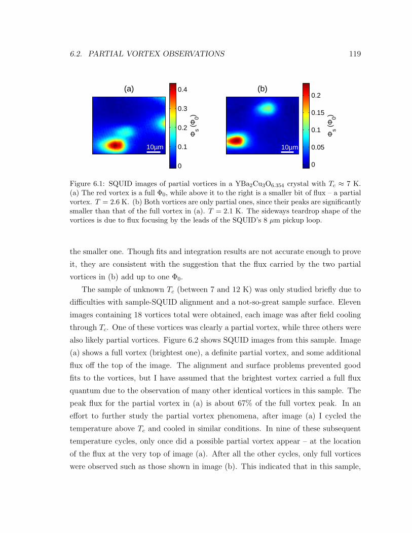
6.2. PARTIAL VORTEX OBSERVATIONS 119
Φs (
Φ0)
0
0.1
0.2
0.3
0.4(a)
10µm
Φs (
Φ0)
0
0.05
0.1
0.15
0.2 (b)
10µm
Figure 6.1: SQUID images of partial vortices in a YBa2Cu3O6.354 crystal with Tc ≈ 7 K.(a) The red vortex is a full Φ0, while above it to the right is a smaller bit of flux – a partialvortex. T = 2.6 K. (b) Both vortices are only partial ones, since their peaks are significantlysmaller than that of the full vortex in (a). T = 2.1 K. The sideways teardrop shape of thevortices is due to flux focusing by the leads of the SQUID’s 8 µm pickup loop.
the smaller one. Though fits and integration results are not accurate enough to prove
it, they are consistent with the suggestion that the flux carried by the two partial
vortices in (b) add up to one Φ0.
The sample of unknown Tc (between 7 and 12 K) was only studied briefly due to
difficulties with sample-SQUID alignment and a not-so-great sample surface. Eleven
images containing 18 vortices total were obtained, each image was after field cooling
through Tc. One of these vortices was clearly a partial vortex, while three others were
also likely partial vortices. Figure 6.2 shows SQUID images from this sample. Image
(a) shows a full vortex (brightest one), a definite partial vortex, and some additional
flux off the top of the image. The alignment and surface problems prevented good
fits to the vortices, but I have assumed that the brightest vortex carried a full flux
quantum due to the observation of many other identical vortices in this sample. The
peak flux for the partial vortex in (a) is about 67% of the full vortex peak. In an
effort to further study the partial vortex phenomena, after image (a) I cycled the
temperature above Tc and cooled in similar conditions. In nine of these subsequent
temperature cycles, only once did a possible partial vortex appear – at the location
of the flux at the very top of image (a). After all the other cycles, only full vortices
were observed such as those shown in image (b). This indicated that in this sample,
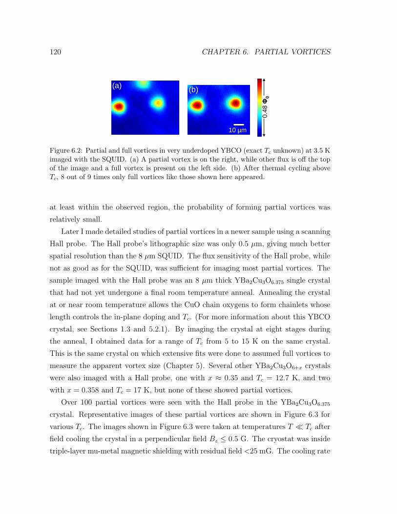
120 CHAPTER 6. PARTIAL VORTICES
0.48
ΦΦ ΦΦ0
(a)
10 µm
(b)
Figure 6.2: Partial and full vortices in very underdoped YBCO (exact Tc unknown) at 3.5 Kimaged with the SQUID. (a) A partial vortex is on the right, while other flux is off the topof the image and a full vortex is present on the left side. (b) After thermal cycling aboveTc, 8 out of 9 times only full vortices like those shown here appeared.
at least within the observed region, the probability of forming partial vortices was
relatively small.
Later I made detailed studies of partial vortices in a newer sample using a scanning
Hall probe. The Hall probe’s lithographic size was only 0.5 µm, giving much better
spatial resolution than the 8 µm SQUID. The flux sensitivity of the Hall probe, while
not as good as for the SQUID, was sufficient for imaging most partial vortices. The
sample imaged with the Hall probe was an 8 µm thick YBa2Cu3O6.375 single crystal
that had not yet undergone a final room temperature anneal. Annealing the crystal
at or near room temperature allows the CuO chain oxygens to form chainlets whose
length controls the in-plane doping and Tc. (For more information about this YBCO
crystal, see Sections 1.3 and 5.2.1). By imaging the crystal at eight stages during
the anneal, I obtained data for a range of Tc from 5 to 15 K on the same crystal.
This is the same crystal on which extensive fits were done to assumed full vortices to
measure the apparent vortex size (Chapter 5). Several other YBa2Cu3O6+x crystals
were also imaged with a Hall probe, one with x ≈ 0.35 and Tc = 12.7 K, and two
with x = 0.358 and Tc = 17 K, but none of these showed partial vortices.
Over 100 partial vortices were seen with the Hall probe in the YBa2Cu3O6.375
crystal. Representative images of these partial vortices are shown in Figure 6.3 for
various Tc. The images shown in Figure 6.3 were taken at temperatures T ¿ Tc after
field cooling the crystal in a perpendicular field Bz ≤ 0.5 G. The cryostat was inside
triple-layer mu-metal magnetic shielding with residual field <25 mG. The cooling rate
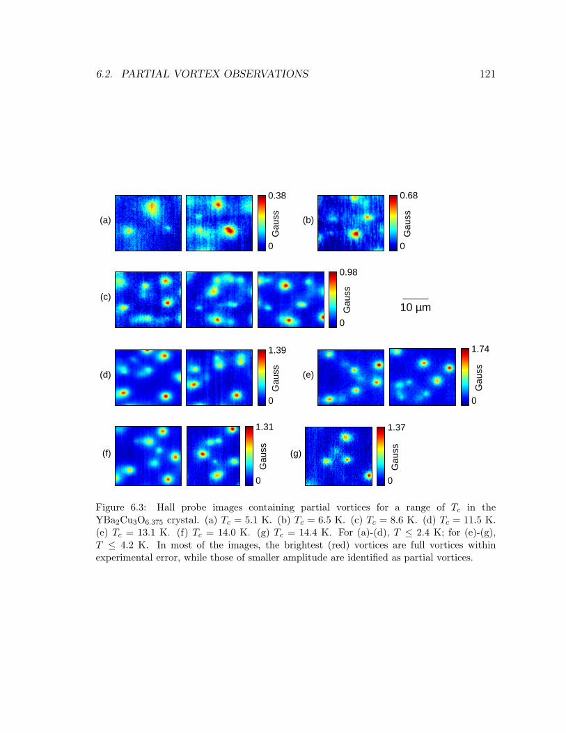
6.2. PARTIAL VORTEX OBSERVATIONS 121
(a) (b)
(c)
(d) (e)
(f) (g)
Gau
ss
0.38
0
Gau
ss
0.68
0
Gau
ss
0.98
0
Gau
ss
1.39
0
Gau
ss
1.74
0
Gau
ss
1.31
0
Gau
ss
1.37
0
10 µm
Figure 6.3: Hall probe images containing partial vortices for a range of Tc in theYBa2Cu3O6.375 crystal. (a) Tc = 5.1 K. (b) Tc = 6.5 K. (c) Tc = 8.6 K. (d) Tc = 11.5 K.(e) Tc = 13.1 K. (f) Tc = 14.0 K. (g) Tc = 14.4 K. For (a)-(d), T ≤ 2.4 K; for (e)-(g),T ≤ 4.2 K. In most of the images, the brightest (red) vortices are full vortices withinexperimental error, while those of smaller amplitude are identified as partial vortices.
122 CHAPTER 6. PARTIAL VORTICES
was typically 3 K/min through the superconducting transition, since that was the rate
the sample chamber cooled when the heater was turned off after warming the sample
above Tc. Cooling ten times slower did not reduce the number of partial vortices. The
images were typically taken after the applied field was turned off. Images before and
after turning off the field at low temperature looked identical. As previous experience
with these crystals has also showed, there are plenty of pinning sites in these crystals
such that for low fields the vortices do not escape when the field is turned off. (It
is typical to observe isolated pinned vortices in a field-cooled sample for most type
II superconductors.) When the sample was cooled in zero field, no vortices (partial
or full) were present. I also took images of partial vortices in other situations such
as after cooling in fields with a large horizontal component, and after cycling the
temperature to values near but below Tc. These data will be discussed below.
6.2.1 Properties
Many properties of the partial vortices can be deduced from my data. Partial
vortices are seen only in crystals with low Tc. Previous imaging of near-optimally
doped (Tc = 92 K) and Ortho-II (Tc = 60 K) YBCO crystals showed no partial
vortices. They occur frequently for the lowest Tc’s and are rare for Tc & 12 K.
The flux carried by the partial vortices is not limited to Φ0/2 or other small integer
fractions, rather it seems to vary continuously. The frequency of occurrence and the
flux carried by the partial vortices will be discussed quantitatively in Section 6.2.2.
Another observation is that partial vortices tend to occur in groups. This is an
important property, because it is consistent with the idea that the partial vortices
occur in a group that as a whole sum to one flux quantum. Partial vortices have
been observed up to tens-of-microns away from other partial vortices within a group.
Thus in cases where a partial vortex appears isolated, others might be nearby but
not within the image area. The partial vortices usually have clear peaks, can have
circular symmetry like a full vortex, or sometimes they are elongated or have a faint
trail of flux (refer to Figure 6.3 for examples).
Partial vortices show a tendency to prefer certain regions of the crystal, even after
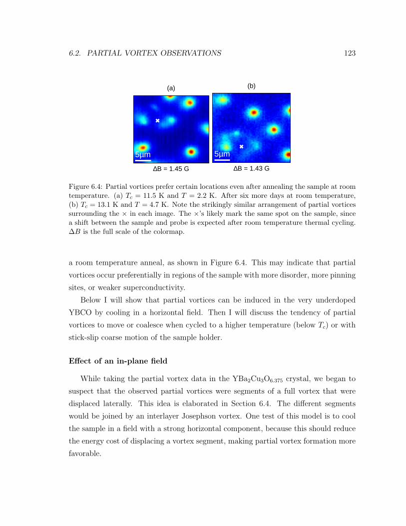
6.2. PARTIAL VORTEX OBSERVATIONS 123
∆B = 1.45 G
(a)
5µm
∆B = 1.43 G
(b)
5µm
Figure 6.4: Partial vortices prefer certain locations even after annealing the sample at roomtemperature. (a) Tc = 11.5 K and T = 2.2 K. After six more days at room temperature,(b) Tc = 13.1 K and T = 4.7 K. Note the strikingly similar arrangement of partial vorticessurrounding the × in each image. The ×’s likely mark the same spot on the sample, sincea shift between the sample and probe is expected after room temperature thermal cycling.∆B is the full scale of the colormap.
a room temperature anneal, as shown in Figure 6.4. This may indicate that partial
vortices occur preferentially in regions of the sample with more disorder, more pinning
sites, or weaker superconductivity.
Below I will show that partial vortices can be induced in the very underdoped
YBCO by cooling in a horizontal field. Then I will discuss the tendency of partial
vortices to move or coalesce when cycled to a higher temperature (below Tc) or with
stick-slip coarse motion of the sample holder.
Effect of an in-plane field
While taking the partial vortex data in the YBa2Cu3O6.375 crystal, we began to
suspect that the observed partial vortices were segments of a full vortex that were
displaced laterally. This idea is elaborated in Section 6.4. The different segments
would be joined by an interlayer Josephson vortex. One test of this model is to cool
the sample in a field with a strong horizontal component, because this should reduce
the energy cost of displacing a vortex segment, making partial vortex formation more
favorable.
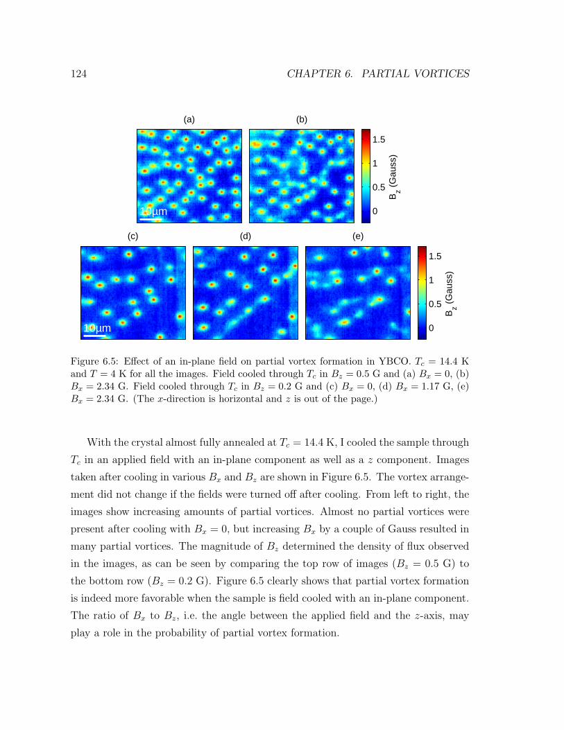
124 CHAPTER 6. PARTIAL VORTICES
0
0.5
1
1.5
0
0.5
1
1.5
(a)
10µm
Bz (
Gau
ss)
(b)
(c)
10µm
(d)
Bz (
Gau
ss)
(e)
Figure 6.5: Effect of an in-plane field on partial vortex formation in YBCO. Tc = 14.4 Kand T = 4 K for all the images. Field cooled through Tc in Bz = 0.5 G and (a) Bx = 0, (b)Bx = 2.34 G. Field cooled through Tc in Bz = 0.2 G and (c) Bx = 0, (d) Bx = 1.17 G, (e)Bx = 2.34 G. (The x-direction is horizontal and z is out of the page.)
With the crystal almost fully annealed at Tc = 14.4 K, I cooled the sample through
Tc in an applied field with an in-plane component as well as a z component. Images
taken after cooling in various Bx and Bz are shown in Figure 6.5. The vortex arrange-
ment did not change if the fields were turned off after cooling. From left to right, the
images show increasing amounts of partial vortices. Almost no partial vortices were
present after cooling with Bx = 0, but increasing Bx by a couple of Gauss resulted in
many partial vortices. The magnitude of Bz determined the density of flux observed
in the images, as can be seen by comparing the top row of images (Bz = 0.5 G) to
the bottom row (Bz = 0.2 G). Figure 6.5 clearly shows that partial vortex formation
is indeed more favorable when the sample is field cooled with an in-plane component.
The ratio of Bx to Bz, i.e. the angle between the applied field and the z-axis, may
play a role in the probability of partial vortex formation.
6.2. PARTIAL VORTEX OBSERVATIONS 125
Mobility
I found that partial vortices were much more mobile than full conventional vor-
tices in the same samples. This was observed in two ways. One method showed that
partial vortices moved around when the temperature was raised to T < Tc. Other ob-
servations with both the SQUID and Hall probe showed partial vortices which moved
or coalesced when subjected to sample coarse motion. Both of these observations
suggest that the partial vortices are less strongly pinned than full vortices.
To qualitatively compare the pinning strength of partial and full vortices, I raised
the temperature and observed whether the vortices moved. This was done in a con-
trolled manner as follows. The YBa2Cu3O6.375 sample with Tc = 14.4 K was cooled
to 3 K in a field ~B = 2x + 0.25z G. The large x-component was chosen to induce
partial vortices. While at 3 K the applied field was turned off and no change in the
vortex arrangement was observed. Then the sample was warmed up to T = 6.6 K,
cooled back to 3 K, and imaged again. This cycle was repeated several times with
successively higher maximum temperatures below Tc. After all cycles, the vortices
had moved. The images are shown in Figure 6.6(a). Full vortices created by cooling
through Tc in ~B = 0.25z G did not show any motion after similar thermal cycling
(Figure 6.6(b)).
Motion of partial vortices was also observed at times after stick-slip coarse motion
of the sample holder in the z direction or the xy plane. Sometimes partial vortices
appeared to coalesce. Figure 6.7 shows Hall probe images before and after several
ramps of the voltage on the z piezo (to determine sample-probe separation) and slight
z coarse motion towards the sample. Two partial vortices of approximately the same
peak amplitude (shown circled) in the before image appeared to coalesce into one
brighter vortex. The vortices are rather close to the left edge of the image, so it is
possible that other flux outside the image area participated in the change and that
these images do not show the full story. Nonetheless, the partial vortices definitely
moved and probably coalesced due to the z motion.
Figure 6.8 shows SQUID images of a partial vortex that moved with respect to
the sample and to stationary larger vortices when the sample was moved in the y
direction with stick-slip coarse motion. [Image (a) in this figure is the same as Figure
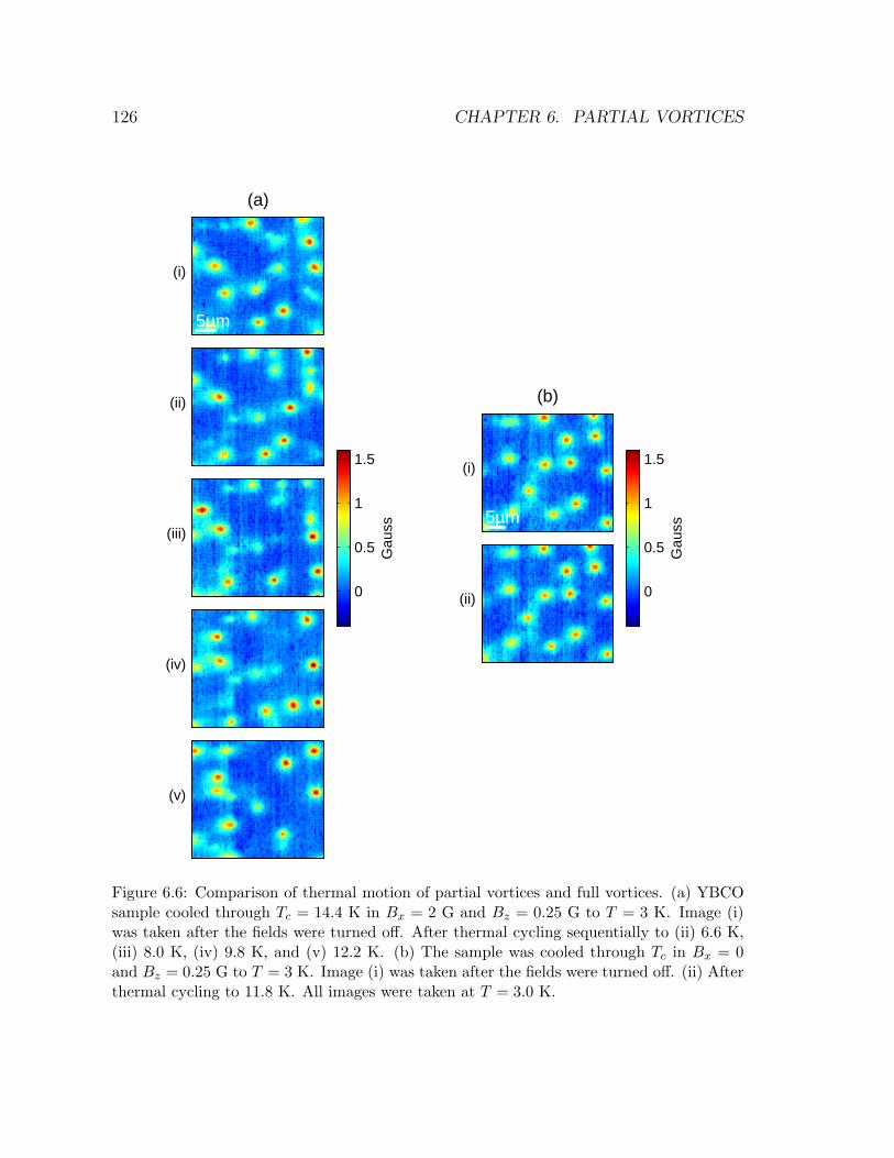
126 CHAPTER 6. PARTIAL VORTICES
Gau
ss
0
0.5
1
1.5
Gau
ss
0
0.5
1
1.5
(a)
5µm
(i)
(ii)
(iii)
(iv)
(v)
(b)
5µm
(i)
(ii)
Figure 6.6: Comparison of thermal motion of partial vortices and full vortices. (a) YBCOsample cooled through Tc = 14.4 K in Bx = 2 G and Bz = 0.25 G to T = 3 K. Image (i)was taken after the fields were turned off. After thermal cycling sequentially to (ii) 6.6 K,(iii) 8.0 K, (iv) 9.8 K, and (v) 12.2 K. (b) The sample was cooled through Tc in Bx = 0and Bz = 0.25 G to T = 3 K. Image (i) was taken after the fields were turned off. (ii) Afterthermal cycling to 11.8 K. All images were taken at T = 3.0 K.
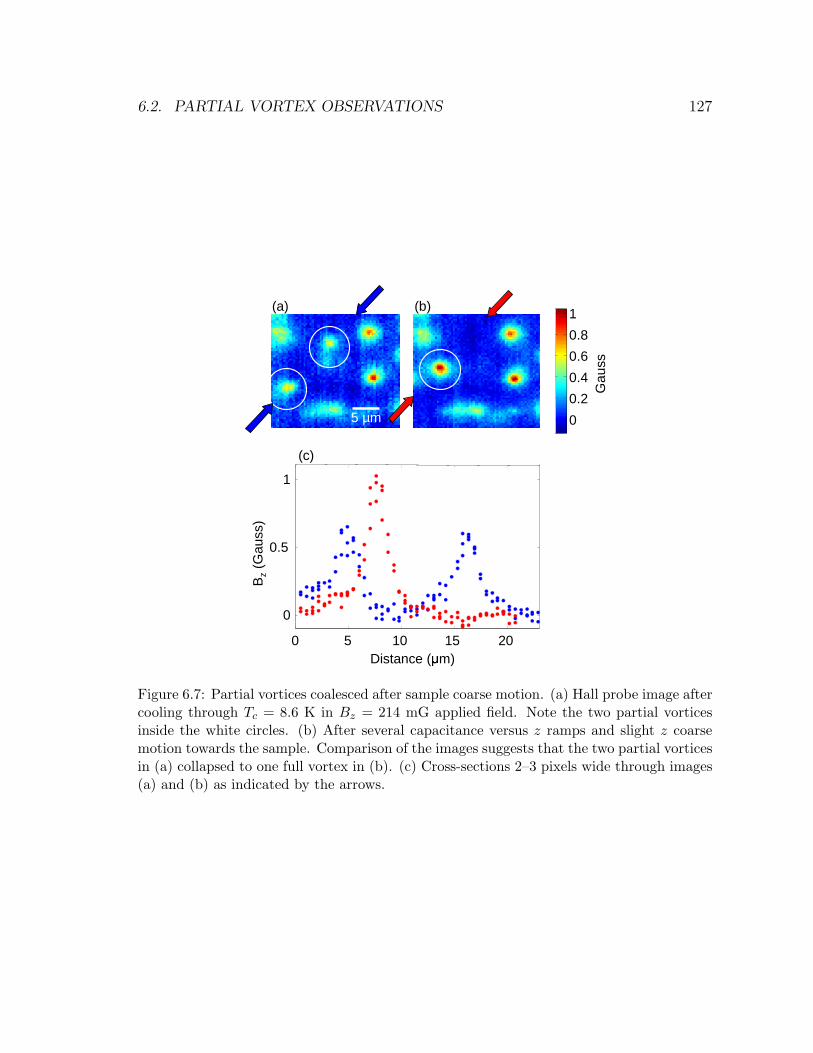
6.2. PARTIAL VORTEX OBSERVATIONS 127
0
0.2
0.4
0.6
0.8
1
Gau
ss
5 µm
0 5 10 15 20
0
0.5
1
Distance ( m)
Bz
(Gau
ss)
(a) (b)
(c)
Figure 6.7: Partial vortices coalesced after sample coarse motion. (a) Hall probe image aftercooling through Tc = 8.6 K in Bz = 214 mG applied field. Note the two partial vorticesinside the white circles. (b) After several capacitance versus z ramps and slight z coarsemotion towards the sample. Comparison of the images suggests that the two partial vorticesin (a) collapsed to one full vortex in (b). (c) Cross-sections 2–3 pixels wide through images(a) and (b) as indicated by the arrows.
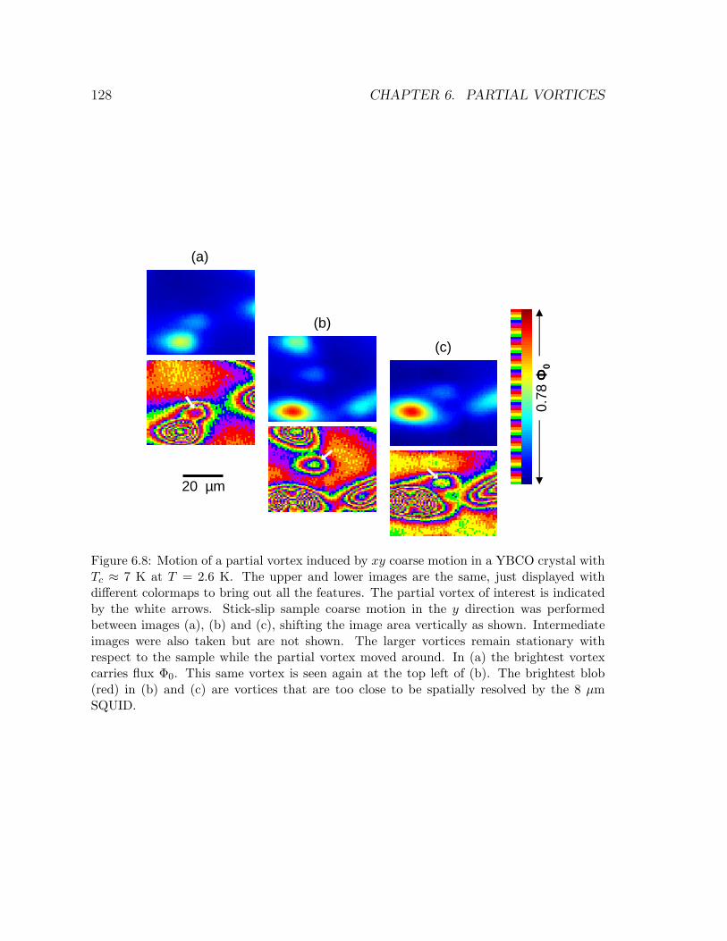
128 CHAPTER 6. PARTIAL VORTICES
0.78
ΦΦ ΦΦ0
20 µm
(a)
(b)
(c)
Figure 6.8: Motion of a partial vortex induced by xy coarse motion in a YBCO crystal withTc ≈ 7 K at T = 2.6 K. The upper and lower images are the same, just displayed withdifferent colormaps to bring out all the features. The partial vortex of interest is indicatedby the white arrows. Stick-slip sample coarse motion in the y direction was performedbetween images (a), (b) and (c), shifting the image area vertically as shown. Intermediateimages were also taken but are not shown. The larger vortices remain stationary withrespect to the sample while the partial vortex moved around. In (a) the brightest vortexcarries flux Φ0. This same vortex is seen again at the top left of (b). The brightest blob(red) in (b) and (c) are vortices that are too close to be spatially resolved by the 8 µmSQUID.
6.2. PARTIAL VORTEX OBSERVATIONS 129
6.1(a)]. The partial vortex has approximately 40% the peak flux of the full vortex in
(a). If this partial vortex is part of a group, it is not clear where the other members
of the group are. The other partial flux might be outside the image area, or could be
within the unresolved bright flux blob in images (b) and (c).
The motion of partial vortices during coarse motion of the sample holder could
be due to stray fields created by the high voltage pulses required to induce the stick-
slip motion. The stray fields might interact with the vortex fields creating forces on
the vortices that are only large enough to unpin and move the partial vortices. The
fact that partial vortices are mobile at temperatures quite below Tc and under the
influence of sample coarse motion, while full vortices generally are not, shows that
partial vortices are not as strongly pinned as full vortices.
6.2.2 Statistics
In this section I will give some statistics on the frequency of occurrence and magni-
tude of the partial vortices observed with the Hall probe in the YBa2Cu3O6.375 crystal
with varied Tc. The numbers presented here should be taken as indicators rather than
statistically rigorous data for the following reasons: A finite number of images were
taken at each Tc, the images covered a small area (maximum of 45×45 µm2) and were
taken over a small fraction of the crystal surface, and it was difficult to identify a very
weak partial vortex or to distinguish a nearly full vortex from a full vortex especially
at the lowest Tc where apparent vortex size was largest and inhomogeneous (Chapter
5). Nonetheless, two facts will be clear: (1) The percentage of partial vortices falls
off, from >50% to just a few %, as Tc increases from 5 to 15 K. (2) The magnitude of
the partial vortices varies continuously and does not seem limited to certain fractions.
From images at each Tc for the Hall probe YBCO sample, I counted the numbers of
full vortices and partial vortices in unique images which were field cooled in an applied
perpendicular field (Bz only). A partial vortex was taken to be any distinct blob of
flux with an identifiable peak and a magnitude smaller than nearby full vortices.
Vortices that I could not identify as clearly full or partial (a difficulty especially for
the Tc = 5.1 K data) were left out of the count. Table 6.1 gives the results. Over
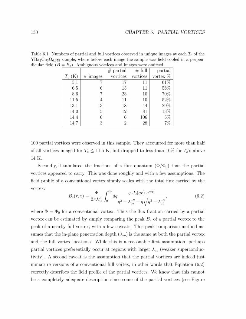
130 CHAPTER 6. PARTIAL VORTICES
Table 6.1: Numbers of partial and full vortices observed in unique images at each Tc of theYBa2Cu3O6.375 sample, where before each image the sample was field cooled in a perpen-dicular field (B = Bz). Ambiguous vortices and images were omitted.
# partial # full partialTc (K) # images vortices vortices vortex %
5.1 7 17 11 61%6.5 6 15 11 58%8.6 7 23 10 70%
11.5 4 11 10 52%13.1 13 18 44 29%14.0 5 12 81 13%14.4 6 6 106 5%14.7 3 2 28 7%
100 partial vortices were observed in this sample. They accounted for more than half
of all vortices imaged for Tc ≤ 11.5 K, but dropped to less than 10% for Tc’s above
14 K.
Secondly, I tabulated the fractions of a flux quantum (Φ/Φ0) that the partial
vortices appeared to carry. This was done roughly and with a few assumptions. The
field profile of a conventional vortex simply scales with the total flux carried by the
vortex:
Bz(r, z) =Φ
2πλ2ab
∫ ∞
0
dqq J0(qr) e−qz
q2 + λ−2ab + q
√q2 + λ−2
ab
, (6.2)
where Φ = Φ0 for a conventional vortex. Thus the flux fraction carried by a partial
vortex can be estimated by simply comparing the peak Bz of a partial vortex to the
peak of a nearby full vortex, with a few caveats. This peak comparison method as-
sumes that the in-plane penetration depth (λab) is the same at both the partial vortex
and the full vortex locations. While this is a reasonable first assumption, perhaps
partial vortices preferentially occur at regions with larger λab (weaker superconduc-
tivity). A second caveat is the assumption that the partial vortices are indeed just
miniature versions of a conventional full vortex, in other words that Equation (6.2)
correctly describes the field profile of the partial vortices. We know that this cannot
be a completely adequate description since some of the partial vortices (see Figure
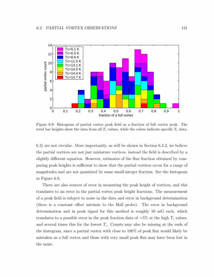
6.2. PARTIAL VORTEX OBSERVATIONS 131
0 0.1 0.2 0.3 0.4 0.5 0.6 0.7 0.8 0.9 10
2
4
6
8
10
12
14
fraction of a full vortex
part
ial v
orte
x co
unt
Tc=5.1 KTc=6.5 KTc=8.6 KTc=11.5 KTc=13.1 KTc=14.0 KTc=14.4 KTc=14.7 K
Figure 6.9: Histogram of partial vortex peak field as a fraction of full vortex peak. Thetotal bar heights show the data from all Tc values, while the colors indicate specific Tc data.
6.3) are not circular. More importantly, as will be shown in Section 6.4.2, we believe
the partial vortices are not just miniature vortices, instead the field is described by a
slightly different equation. However, estimates of the flux fraction obtained by com-
paring peak heights is sufficient to show that the partial vortices occur for a range of
magnitudes and are not quantized by some small-integer fraction. See the histogram
in Figure 6.9.
There are also sources of error in measuring the peak height of vortices, and this
translates to an error in the partial vortex peak height fractions. The measurement
of a peak field is subject to noise in the data and error in background determination
(there is a constant offset intrinsic to the Hall probe). The error in background
determination and in peak signal for this method is roughly 50 mG each, which
translates to a possible error in the peak fraction data of ∼5% at the high Tc values,
and several times this for the lowest Tc. Counts may also be missing at the ends of
the histogram, since a partial vortex with close to 100% of peak flux would likely be
mistaken as a full vortex and those with very small peak flux may have been lost in
the noise.
132 CHAPTER 6. PARTIAL VORTICES
6.3 Thoughts and discussion
We considered many ideas in the process of determining what these partial vortices
were before settling on the “split stack” scenario to be discussed in detail in Section
6.4. The ideas ranged from high frequency dynamics, to unconventional behavior of
very small superfluid density, to grain boundaries, and to vortex termination below
the surface.
One of the first ideas considered was that a group of partial vortices was actually
just one full Φ0 vortex that hopped between pinning sites on a time scale much faster
than the measurement. The apparent fraction of Φ0 carried by each partial vortex in
a group would be equal to the fraction of time the full vortex spent at that pinning
site. The time to take one SQUID image was typically 30–60 sec, with a time per
pixel of ∼10 ms. No signature of hopping was seen in the images. For a more concrete
test, we parked the SQUID over a partial vortex and recorded the flux through the
SQUID pickup loop as a function of time. No fluctuations were observed below the
400 Hz roll off of the SQUID electronics. The hopping idea was discarded when the
distances were considered. Partial vortices were often tens-of-microns apart, making
it improbable that the vortex would only hop between a few pinning sites and never
spend time at the many pinning sites in-between. Observations of vortex/anti-vortex
pairs annihilating in these crystals (Gardner et al. 2002) showed that a pair, created
∼13 µm apart, would linger at intermediate pinning sites and/or rachet towards each
other through the pinning landscape. This suggests that a hopping vortex would not
spend time only at pinning sites tens-of-microns apart, but would also visit many
intermediate sites, which would not result in quasi-isolated partial vortices.
Another idea involves unconventional behavior of the very small superfluid density
(ns/m∗) in these very underdoped samples. The following idea is from discussions
with Nazario and Santiago. Flux quantization results from the fluxoid quantization
condition in Equation (6.1) with vs = 0 far from the superconductor. In a well
behaved superconductor, the current density Js = 2ensvs is zero far from a vortex
because vs = 0 while ns > 0. However, if ns was zero, Js could be zero with a
non-zero value of vs. If the superfluid density vanished or had many fluctuating
6.3. THOUGHTS AND DISCUSSION 133
zeros along the integration path, the second term (the vs integral) in Equation (6.1)
could be non-zero even far away from the vortex and the flux Φ could be less than
the flux quantum. This idea requires unusual behavior of the superconductor with
intermingled or wildly fluctuating “normal” (ns = 0) and superconducting regions.
It also does not account for grouping of partial vortices or for the full screening at
low temperatures seen in Hall probe susceptibility data. Thus this idea is unlikely in
light of other more promising scenarios for partial vortices.
The presence of grain boundaries in certain configurations can result in unquan-
tized flux. This has been seen by Kirtley et al. (1995a) in optimally doped YBCO
films that were grown on a patterned substrate such that grain boundaries enclosed
hexagonal and triangular regions which had 45 rotations about the c-axis with re-
spect to the rest of the film. The 45 rotation creates boundaries with both 0 and π
junctions, since YBCO is a d-wave superconductor. The SQUID images from Kirt-
ley et al. (1995a) show that the total flux through any of the closed grain boundaries
defining a triangle or hexagon is an integer multiple of Φ0, but flux of magnitude much
less than Φ0 is localized at different spots along the boundary. Spontaneous small un-
quantized flux has also been observed along the grain boundary of a YBCO film with
a misalignment angle of 45 by Mannhart et al. (1996). They give a model for this
flux stemming from the d-wave character of the order parameter and micro-facetting
at the grain boundary plane. A more recent paper by Mints et al. (2002) reports
images of splintered vortices along such a grain boundary, where several unquantized
fluxes sum to Φ0.
The unquantized flux in grain boundaries discussed above depends on misalign-
ment angles other than 0 or 90 to give an additional π-shift to the phase as a result
of d-wave symmetry. This is not an adequate model for our observations of partial
vortices in the single crystals of YBCO, because there should not be any angles which
result in a winding of π around a closed loop. The four-fold pattern of the d-wave
order parameter is locked to the lattice. It could potentially rotate at a grain bound-
ary (if there were one) by only 90. Any closed loop crossing a 90 boundary would
have to cross twice, resulting in a phase winding of 2π, not π. Thus even if our single
crystal sample was granular (e. g. due to inhomogeneities in the superfluid density),
134 CHAPTER 6. PARTIAL VORTICES
non-quantized flux could not arise by the same means as in the above experiments
where 45 misalignments were present.
However, Kogan proposed that it could be possible even with no π junctions to
have flux distributed over a closed boundary in sub-Φ0 units. He worked out the
flux division between arms of polygon shaped junctions (in particular for triangles)
where none of the arms are π junctions. The ground state of the triangle with no
π junctions has no magnetic flux. Kogan showed that if the one of the arms of a
triangle with only 0 junctions had a different Josephson penetration depth than the
other two arms, and if a total flux of Φ0 was trapped in the triangle, the flux would
split into two unequal parts. One part would reside on the arm with the different
λJ , and the other part would be on the other two arms. The magnitude of each part
depends on the λJ ’s. This could be generalized to a triangle with a different λJ values
for all three arms.
Kogan’s idea could be plausibly applied to our single crystals as the mechanism
for partial vortices if the samples had granularity resulting in closed junctions with
unequal Josephson penetration depths. There is some evidence for inhomogeneity in
the very underdoped YBa2Cu3O6.375 sample. At the lowest measured Tc value of 5.1 K,
the superconducting transition width was ∼3 K, more than twice the width at higher
Tc. Also, the spread in apparent vortex shapes and sizes (Section 5.2.4) measured
from different vortices at the lowest Tc suggests inhomogeneity. Even though there
are not crystallographic grains in the single crystal samples, there might be grains of
weaker and stronger superconductivity.
Another phenomenon that we considered is subsurface vortex termination. Mints
et al. (2000) calculated that in a layered superconductor (like the cuprates) in the limit
of no Josephson coupling between the layers, it is possible for a vortex to terminate
in a layer below the surface and channel at least part of the flux out parallel to the
layers. The energy cost of subsurface termination increases with sample size, but
they show that for sample size below Rc ∼ κλab (where κ = λab/ξab), subsurface
termination becomes energetically favorable. The coherence length ξab is not known
for our very underdoped YBCO crystals, but if we assume the optimally doped value
κ ∼ 5, Rc could be about 5 µm. Our samples are of order 1 mm, but Mints et al.
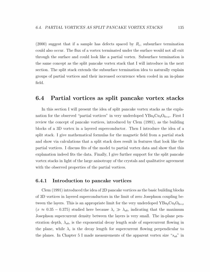
6.4. PARTIAL VORTICES AS SPLIT PANCAKE VORTEX STACKS 135
(2000) suggest that if a sample has defects spaced by Rc, subsurface termination
could also occur. The flux of a vortex terminated under the surface would not all exit
through the surface and could look like a partial vortex. Subsurface termination is
the same concept as the split pancake vortex stack that I will introduce in the next
section. The split stack extends the subsurface termination idea to naturally explain
groups of partial vortices and their increased occurrence when cooled in an in-plane
field.
6.4 Partial vortices as split pancake vortex stacks
In this section I will present the idea of split pancake vortex stacks as the expla-
nation for the observed “partial vortices” in very underdoped YBa2Cu3O6+x. First I
review the concept of pancake vortices, introduced by Clem (1991), as the building
blocks of a 3D vortex in a layered superconductor. Then I introduce the idea of a
split stack. I give mathematical formulas for the magnetic field from a partial stack
and show via calculations that a split stack does result in features that look like the
partial vortices. I discuss fits of the model to partial vortex data and show that this
explanation indeed fits the data. Finally, I give further support for the split pancake
vortex stacks in light of the large anisotropy of the crystals and qualitative agreement
with the observed properties of the partial vortices.
6.4.1 Introduction to pancake vortices
Clem (1991) introduced the idea of 2D pancake vortices as the basic building blocks
of 3D vortices in layered superconductors in the limit of zero Josephson coupling be-
tween the layers. This is an appropriate limit for the very underdoped YBa2Cu3O6+x
(x ≈ 0.35 − 0.375) studied here because λc À λab, indicating that the maximum
Josephson supercurrent density between the layers is very small. The in-plane pen-
etration depth, λab, is the exponential decay length scale of supercurrent flowing in
the plane, while λc is the decay length for supercurrent flowing perpendicular to
the planes. In Chapter 5 I made measurements of the apparent vortex size “sab” in
136 CHAPTER 6. PARTIAL VORTICES
YBa2Cu3O6.375 which gives an upper bound on λab. The results showed sab(T ¿ Tc)
ranging from roughly 0.5 to several microns for Tc ranging from 5–15 K, where the
vortex size decreased with increasing Tc. In contrast, measurements of λc in simi-
lar samples by Hosseini et al. (2003) gave much larger values: λc(0) ≈ 100 µm for
Tc ≈ 6 K, and λc(0) ≈ 40 µm for Tc ≈ 15 K. Thus the anisotropy parameter λc/λab
in our very underdoped YBCO is large, with lower bound in the range 40–80, so the
approximation of zero Josephson coupling (λc →∞) is appropriate for this system.
Clem (1991) begins his discussion by first reviewing the field and current density
from one pancake vortex (carrying flux Φ0) in an isolated superconducting layer with
thickness d ¿ λbulk. The vector potential is
aφ(r, z) =Φ0
2π
∫ ∞
0
dqJ1(qr) e−q|z|
1 + qΛ. (6.3)
Here r is the radial distance from the pancake center, z is the distance from the layer
plane, J1 is the first-order Bessel function, and Λ = 2λ2bulk/d is the 2D screening
length in the layer. The magnetic field can be found simply from B = ∇× a.
If other superconducting layers are present, they act to screen the magnetic field
from the single pancake. Clem (1991) calculated the field from a pancake in a single
layer at z = 0 which is surrounded by an infinite number of other layers above and
below with layer spacing s (which would be the c-axis unit cell dimension in YBCO).
In situations where r and z are much larger than s, the discreteness of the layers can
be ignored and (in the zero Josephson coupling limit) the vector potential is
aφ(r, z) =Φ0λab
2πΛr
(e−|z|/λab − e−
√r2+z2/λab
). (6.4)
From this the magnetic field can be calculated. The field is channelled away from
the pancake parallel to the layers and decays on the length scale λab perpendicular to
the layers. Since λab À s, the field does extend across many layers but is completely
screened out beyond a few λab in the z-direction. The field is such that two pancakes in
the same layer experience a repulsive interaction which is logarithmic for all distances,
but two pancake vortices in different layers experience a weak magnetic attraction
6.4. PARTIAL VORTICES AS SPLIT PANCAKE VORTEX STACKS 137
c-axis
superconducting layers
surface
c-axis
(a) (b)
Figure 6.10: (a) Illustration of a vortex built from 2D pancake vortices. A pancake residesin each layer which are spaced a distance s. (b) Schematic of a split pancake vortex stack.Observed from above, the partial stacks would look like isolated “partial vortices”. Thehorizontal component joining the two partial stacks is an interlayer Josephson vortex.
which favors alignment in z (a pancake stack, as illustrated in Figure 6.10(a)). A
non-zero Josephson coupling would add an additional attractive force.
The total field from many pancake vortices in a system of infinite superconducting
layers can be found from the superposition of Clem’s general vector potential for one
vortex in a system of infinite layers (which I’ve shown in Equation (6.4) only for the
particular limit of small s). Clem shows that a straight stack of 2D pancake vortices,
as shown in Figure 6.10(a), gives the same result as the anisotropic London model for
a 3D vortex. He also calculates the energy of a tilted stack and the thermal energy
required to distort a stack (Clem 1991).
6.4.2 Split pancake stacks
We propose that our observed partial vortices are the top view of partial stacks
of pancake vortices resulting from a split stack. Instead of a stack of 2D pancake
vortices aligned along a single axis in the z-direction, as is favored by pure magnetic
interactions and also by weak Josephson coupling, we propose that other energy
considerations such as pinning make it favorable (as least as local energy minima) to
have the stack split one or more times into partial stacks separated laterally. The
partial stacks would be joined by an interlayer Josephson vortex (where the Josephson
coupling is weak). This picture is schematically shown in Figure 6.10(b). In a top
138 CHAPTER 6. PARTIAL VORTICES
view of the magnetic field, each partial stack that is within a few λab of the surface
would appear as an isolated partial vortex with apparent flux less than Φ0. Whether
or not the stack is split, the 3D vortex would always come all the way through the
sample having one pancake per layer. This explains why the partial vortices always
appear in groups.
The split stack or “kinked structure” was first proposed by Benkraouda and Clem
(1996) as an alternative to a tilted stack. They calculated and compared the energy
of a tilted pancake vortex stack to that of a split stack in the limit of zero Josephson
coupling (λc → 0), with the very top and bottom pancakes pinned. Their calculations
showed that the line tension of a tilted stack is negative for a tilt angle greater than
52 measured from the z-axis, and thus the tilted stack is unstable for large angles.
Even for angles less than 52, they showed that the split stack has lower energy than
a tilted stack for angles greater than ∼5 for stacks containing many pancakes.
An observation of a split pancake vortex stack has been reported by Grigorenko
et al. (2002) in Bi2Sr2CaCu2O8+δ with Tc = 90 K. The split stack in this case was
formed under dynamic conditions and was a rare observation. The primary focus of
their paper was to discuss observations of interacting lattices of pancake vortex stacks
and Josephson (interlayer) vortices. Their observed split (or “fractional”) pancake
stack formed from an aligned stack after the in-plane applied field was suddenly
reduced from 36 Oe to zero. They fit their Hall probe image and obtained ∼0.48 µm
as the depth of the splitting. The stack split a lateral distance of 2.3 µm. Raising
the in-plane field to 11 Oe “healed” the split stack back to a straight stack.
Our partial vortex observations differ from that of Grigorenko et al. (2002) in
BSSCO, in that partial vortices were quite prevalent in the very underdoped YBCO,
especially for very low Tc. Special dynamic situations were not required to produce
partial vortices in the YBCO. They were created simply by field cooling, even in
nominally zero in-plane field. To our knowledge, our partial vortex observations are
the first observation of stable frequently occurring split pancake vortex stacks. The
work by Grigorenko et al. (2002) was performed on optimally doped BSSCO, so it is
quite plausible that imaging studies of BSSCO with lower doping might reveal similar
vortex behavior as in the very underdoped YBCO. This would require improvements
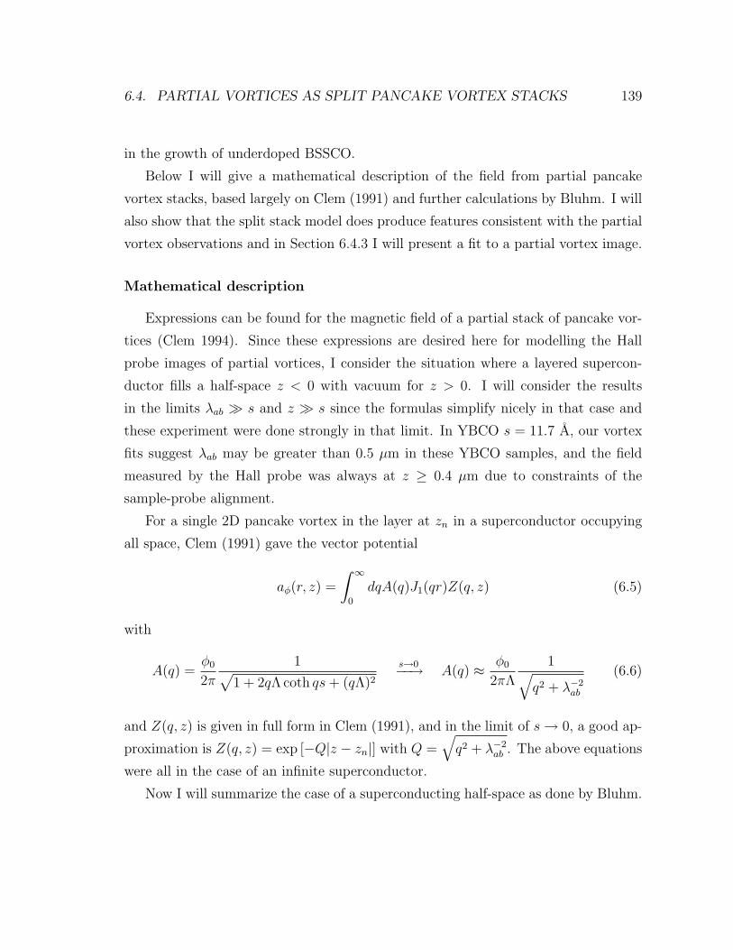
6.4. PARTIAL VORTICES AS SPLIT PANCAKE VORTEX STACKS 139
in the growth of underdoped BSSCO.
Below I will give a mathematical description of the field from partial pancake
vortex stacks, based largely on Clem (1991) and further calculations by Bluhm. I will
also show that the split stack model does produce features consistent with the partial
vortex observations and in Section 6.4.3 I will present a fit to a partial vortex image.
Mathematical description
Expressions can be found for the magnetic field of a partial stack of pancake vor-
tices (Clem 1994). Since these expressions are desired here for modelling the Hall
probe images of partial vortices, I consider the situation where a layered supercon-
ductor fills a half-space z < 0 with vacuum for z > 0. I will consider the results
in the limits λab À s and z À s since the formulas simplify nicely in that case and
these experiment were done strongly in that limit. In YBCO s = 11.7 A, our vortex
fits suggest λab may be greater than 0.5 µm in these YBCO samples, and the field
measured by the Hall probe was always at z ≥ 0.4 µm due to constraints of the
sample-probe alignment.
For a single 2D pancake vortex in the layer at zn in a superconductor occupying
all space, Clem (1991) gave the vector potential
aφ(r, z) =
∫ ∞
0
dqA(q)J1(qr)Z(q, z) (6.5)
with
A(q) =φ0
2π
1√1 + 2qΛ coth qs + (qΛ)2
s→0−−→ A(q) ≈ φ0
2πΛ
1√q2 + λ−2
ab
(6.6)
and Z(q, z) is given in full form in Clem (1991), and in the limit of s → 0, a good ap-
proximation is Z(q, z) = exp [−Q|z − zn|] with Q =√
q2 + λ−2ab . The above equations
were all in the case of an infinite superconductor.
Now I will summarize the case of a superconducting half-space as done by Bluhm.
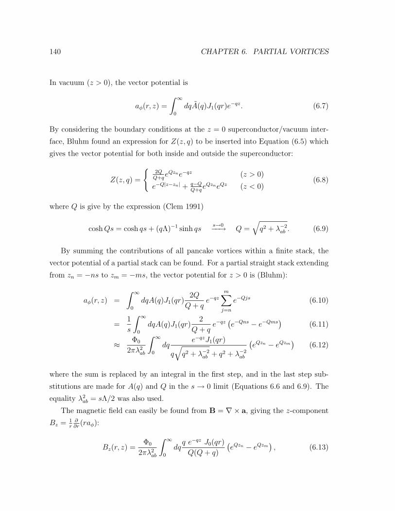
140 CHAPTER 6. PARTIAL VORTICES
In vacuum (z > 0), the vector potential is
aφ(r, z) =
∫ ∞
0
dqA(q)J1(qr)e−qz. (6.7)
By considering the boundary conditions at the z = 0 superconductor/vacuum inter-
face, Bluhm found an expression for Z(z, q) to be inserted into Equation (6.5) which
gives the vector potential for both inside and outside the superconductor:
Z(z, q) =
2Q
Q+qeQzne−qz (z > 0)
e−Q|z−zn| + q−QQ+q
eQzneQz (z < 0)(6.8)
where Q is give by the expression (Clem 1991)
cosh Qs = cosh qs + (qΛ)−1 sinh qss→0−−→ Q =
√q2 + λ−2
ab . (6.9)
By summing the contributions of all pancake vortices within a finite stack, the
vector potential of a partial stack can be found. For a partial straight stack extending
from zn = −ns to zm = −ms, the vector potential for z > 0 is (Bluhm):
aφ(r, z) =
∫ ∞
0
dqA(q)J1(qr)2Q
Q + qe−qz
m∑j=n
e−Qjs (6.10)
=1
s
∫ ∞
0
dqA(q)J1(qr)2
Q + qe−qz
(e−Qns − e−Qms
)(6.11)
≈ Φ0
2πλ2ab
∫ ∞
0
dqe−qzJ1(qr)
q√
q2 + λ−2ab + q2 + λ−2
ab
(eQzn − eQzm
)(6.12)
where the sum is replaced by an integral in the first step, and in the last step sub-
stitutions are made for A(q) and Q in the s → 0 limit (Equations 6.6 and 6.9). The
equality λ2ab = sΛ/2 was also used.
The magnetic field can easily be found from B = ∇× a, giving the z-component
Bz = 1r
∂∂r
(raφ):
Bz(r, z) =Φ0
2πλ2ab
∫ ∞
0
dqq e−qz J0(qr)
Q(Q + q)
(eQzn − eQzm
), (6.13)
6.4. PARTIAL VORTICES AS SPLIT PANCAKE VORTEX STACKS 141
where Q =√
q2 + λ−2ab if conventional units are used in the integral, or alternatively
Q =√
q2 + 1 if r, the z’s, and q are in units of λab (inverse λab for q) in the integrand.
The partial stack begins at a depth zm in the superconductor and terminates at zn.
Since the stack begins and ends within the superconductor, −∞ ≤ zm < zn ≤ 0.
Note that if the partial stack extends from zm = −∞ to zn = 0, Equation (6.13)
becomes simply that of a conventional 3D vortex described by Equation (6.2) with
Φ = Φ0.
The total flux through the top of the crystal resulting from a partial stack can
also be calculated. Clem (1994) gives expressions for the total flux through the top
and bottom of a finite crystal from a single pancake vortex. By integrating over all
pancake vortices in a partial stack, we obtain for the total flux through the z = 0
surface of a superconducting half space for a partial vortex extending from zm to zn
(zm < zn ≤ 0)
Φ = Φ0
(ezn/λab − ezm/λab
). (6.14)
It is easily see that if a straight complete vortex stack (–∞ to 0) splits once at a depth
z = −d, the total flux through the surface from the lower partial stack is Φlower =
Φ0e−d/λab while the flux from the upper partial stack is Φupper = Φ0
(1− e−d/λab
)=
Φ0 − Φlower. The sum of the flux from each segment of the stack is Φ0 as expected.
Notice that if d is greater than several penetration depths, a negligible amount of flux
from the lower partial stack will be observed and the upper partial stack looks just
like a full pancake vortex stack with a full flux quantum.
In this split stack proposal for the partial vortices, it should be emphasized that
these features are “partial” vortices only in the sense that a full flux quantum does not
exit through the surface from one lone partial vortex, even though each 2D pancake
vortex in a layer carries Φ0. Thus there is not some topological funny business going
on creating a “fractional” vortex and violating flux quantization. The unique feature
observed here is a lateral displacement of part of a vortex, best described in the 2D
pancake vortex formulation, and only possible in highly anisotropic crystals.
142 CHAPTER 6. PARTIAL VORTICES
Model split stacks
To get a sense of what a split stack looks like, I generated Bz images from Equation
(6.13) in the case of a straight full stack which splits once at z = −d for several
different d > 0 depth values. For these calculations I set the height above the sample
to be z = 0.8λab, which if λab ≈ 1, is a reasonable value for the sample-probe height.
Figure 6.11 shows the calculated images for a split pancake vortex stack for several
values of split depth d. Cross sections through the field profiles of split vortices as a
function of d are shown in Figure 6.12. If d is a few or more times the penetration
depth λab, only the upper partial stack is seen and its field profile looks like that of a
full vortex. This is because the field from pancakes deep in the sample are completely
screened. A group of N partial vortices could be modelled simply by letting the
pancake vortex stack split N − 1 times at varying depths.
One thing that is easily seen from Equation (6.13) is that if the magnetic field
from all the partial vortices of one group is superimposed, the sum of the fields is
identical to the field profile of a full vortex, assuming the penetration depth λab is
the same at the location of each partial stack. A simplified version of this statement
is that the peak amplitudes of partial vortex stacks within one group should equal
the peak amplitude of a full vortex. This is a quick way to identify a partial vortex
group in the Hall probe images. Another feature worthy of mention is that, at least
for a stack with one split, the Bz from the lower partial stack is more spread out (has
a larger normalized FWHM) than from the upper stack, when compared at constant
z > 0. This can be seen in Figure 6.12 where the partial vortex on the left side is
the lower one. These two features – the sum of the partial vortex fields add to a full
vortex, and the lower partial vortex is more spread out – are helpful in analyzing the
partial vortex data.
6.4.3 Fitting the data
Now I will discuss a fit to a pair of partial vortices to show that the split pancake
stack model is quite consistent with the data.
The image in Figure 6.13(a) shows three uniform full vortices (brightest) and
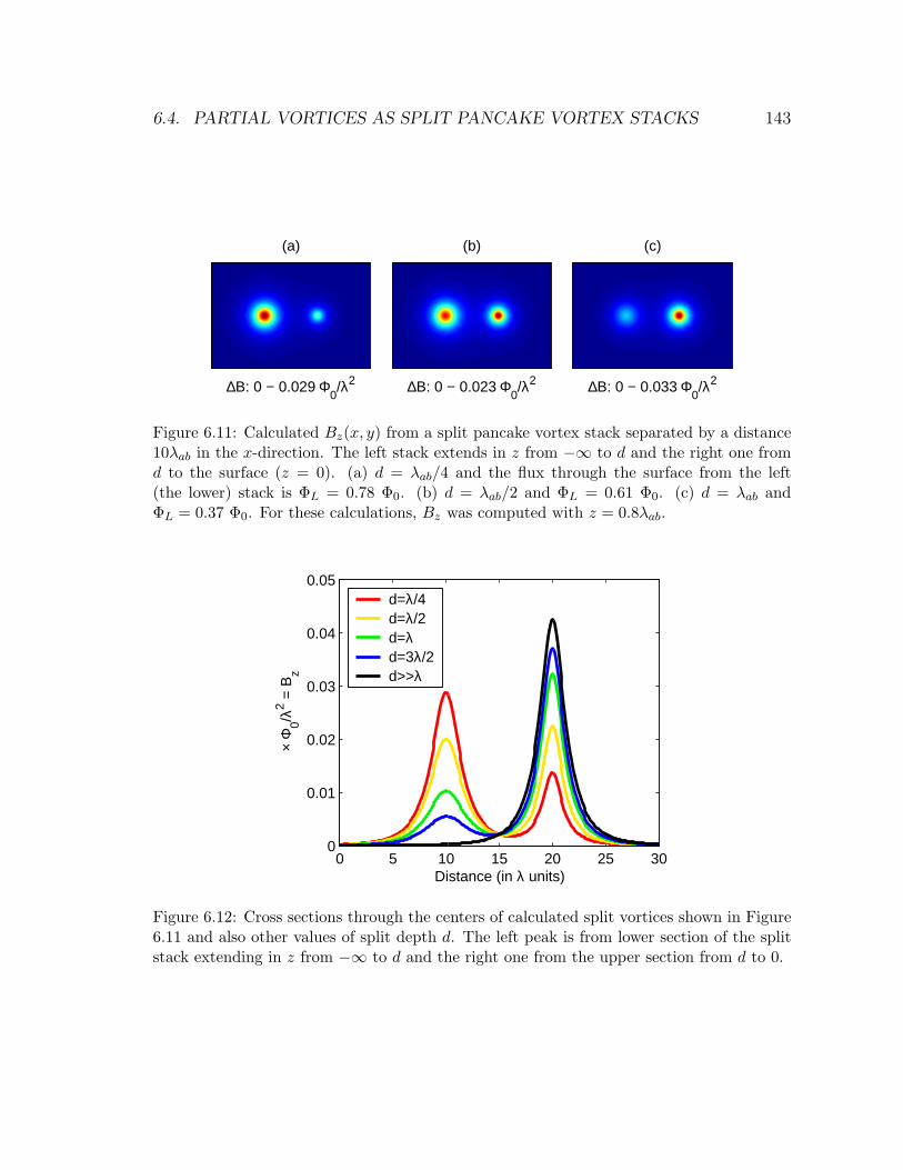
6.4. PARTIAL VORTICES AS SPLIT PANCAKE VORTEX STACKS 143
∆B: 0 − 0.029 Φ0/λ2
(a)
∆B: 0 − 0.023 Φ0/λ2
(b)
∆B: 0 − 0.033 Φ0/λ2
(c)
Figure 6.11: Calculated Bz(x, y) from a split pancake vortex stack separated by a distance10λab in the x-direction. The left stack extends in z from −∞ to d and the right one fromd to the surface (z = 0). (a) d = λab/4 and the flux through the surface from the left(the lower) stack is ΦL = 0.78 Φ0. (b) d = λab/2 and ΦL = 0.61 Φ0. (c) d = λab andΦL = 0.37 Φ0. For these calculations, Bz was computed with z = 0.8λab.
0 5 10 15 20 25 300
0.01
0.02
0.03
0.04
0.05
Distance (in λ units)
× Φ
0/λ2 =
Bz
d=λ/4d=λ/2d=λd=3λ/2d>>λ
Figure 6.12: Cross sections through the centers of calculated split vortices shown in Figure6.11 and also other values of split depth d. The left peak is from lower section of the splitstack extending in z from −∞ to d and the right one from the upper section from d to 0.
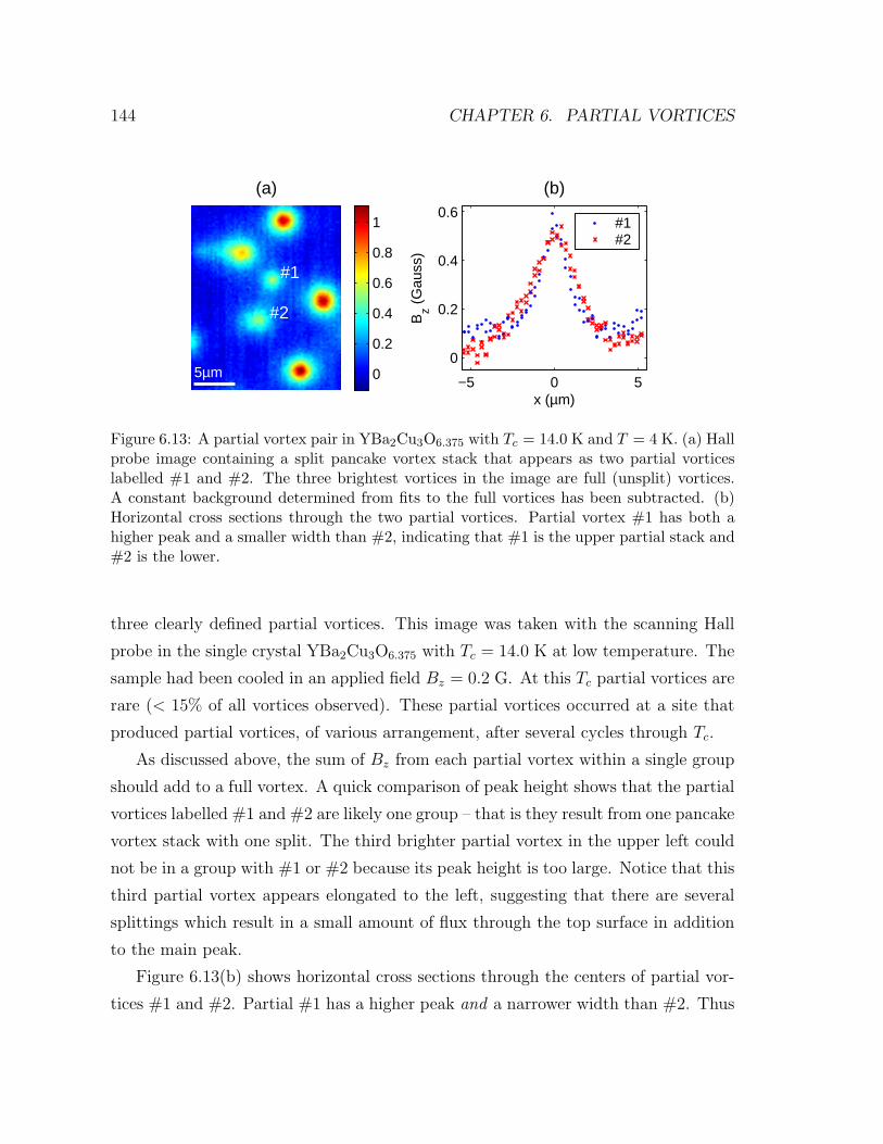
144 CHAPTER 6. PARTIAL VORTICES
0
0.2
0.4
0.6
0.8
1
(a)
5µm
#1
#2
−5 0 5
0
0.2
0.4
0.6
x (µm)B
z (G
auss
)
(b)
#1#2
Figure 6.13: A partial vortex pair in YBa2Cu3O6.375 with Tc = 14.0 K and T = 4 K. (a) Hallprobe image containing a split pancake vortex stack that appears as two partial vorticeslabelled #1 and #2. The three brightest vortices in the image are full (unsplit) vortices.A constant background determined from fits to the full vortices has been subtracted. (b)Horizontal cross sections through the two partial vortices. Partial vortex #1 has both ahigher peak and a smaller width than #2, indicating that #1 is the upper partial stack and#2 is the lower.
three clearly defined partial vortices. This image was taken with the scanning Hall
probe in the single crystal YBa2Cu3O6.375 with Tc = 14.0 K at low temperature. The
sample had been cooled in an applied field Bz = 0.2 G. At this Tc partial vortices are
rare (< 15% of all vortices observed). These partial vortices occurred at a site that
produced partial vortices, of various arrangement, after several cycles through Tc.
As discussed above, the sum of Bz from each partial vortex within a single group
should add to a full vortex. A quick comparison of peak height shows that the partial
vortices labelled #1 and #2 are likely one group – that is they result from one pancake
vortex stack with one split. The third brighter partial vortex in the upper left could
not be in a group with #1 or #2 because its peak height is too large. Notice that this
third partial vortex appears elongated to the left, suggesting that there are several
splittings which result in a small amount of flux through the top surface in addition
to the main peak.
Figure 6.13(b) shows horizontal cross sections through the centers of partial vor-
tices #1 and #2. Partial #1 has a higher peak and a narrower width than #2. Thus
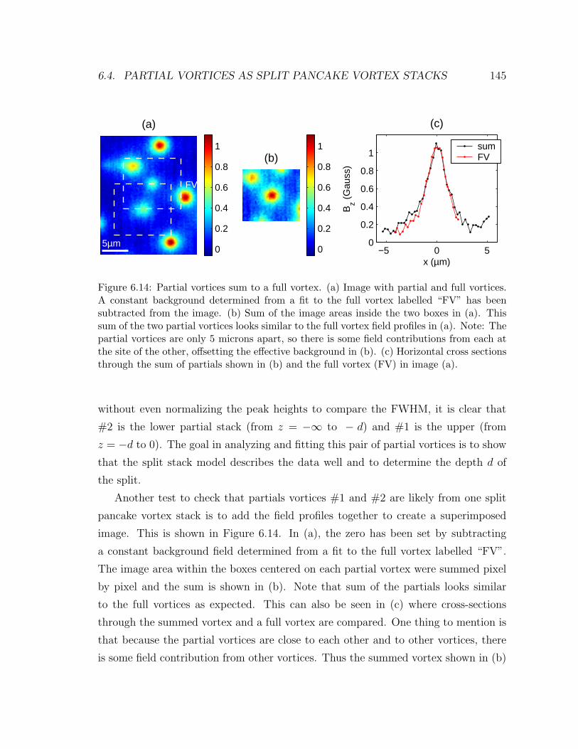
6.4. PARTIAL VORTICES AS SPLIT PANCAKE VORTEX STACKS 145
0
0.2
0.4
0.6
0.8
1
0
0.2
0.4
0.6
0.8
1
(a)
FV
5µm
(b)
−5 0 50
0.2
0.4
0.6
0.8
1
x (µm)
Bz (
Gau
ss)
(c)
sumFV
Figure 6.14: Partial vortices sum to a full vortex. (a) Image with partial and full vortices.A constant background determined from a fit to the full vortex labelled “FV” has beensubtracted from the image. (b) Sum of the image areas inside the two boxes in (a). Thissum of the two partial vortices looks similar to the full vortex field profiles in (a). Note: Thepartial vortices are only 5 microns apart, so there is some field contributions from each atthe site of the other, offsetting the effective background in (b). (c) Horizontal cross sectionsthrough the sum of partials shown in (b) and the full vortex (FV) in image (a).
without even normalizing the peak heights to compare the FWHM, it is clear that
#2 is the lower partial stack (from z = −∞ to − d) and #1 is the upper (from
z = −d to 0). The goal in analyzing and fitting this pair of partial vortices is to show
that the split stack model describes the data well and to determine the depth d of
the split.
Another test to check that partials vortices #1 and #2 are likely from one split
pancake vortex stack is to add the field profiles together to create a superimposed
image. This is shown in Figure 6.14. In (a), the zero has been set by subtracting
a constant background field determined from a fit to the full vortex labelled “FV”.
The image area within the boxes centered on each partial vortex were summed pixel
by pixel and the sum is shown in (b). Note that sum of the partials looks similar
to the full vortices as expected. This can also be seen in (c) where cross-sections
through the summed vortex and a full vortex are compared. One thing to mention is
that because the partial vortices are close to each other and to other vortices, there
is some field contribution from other vortices. Thus the summed vortex shown in (b)
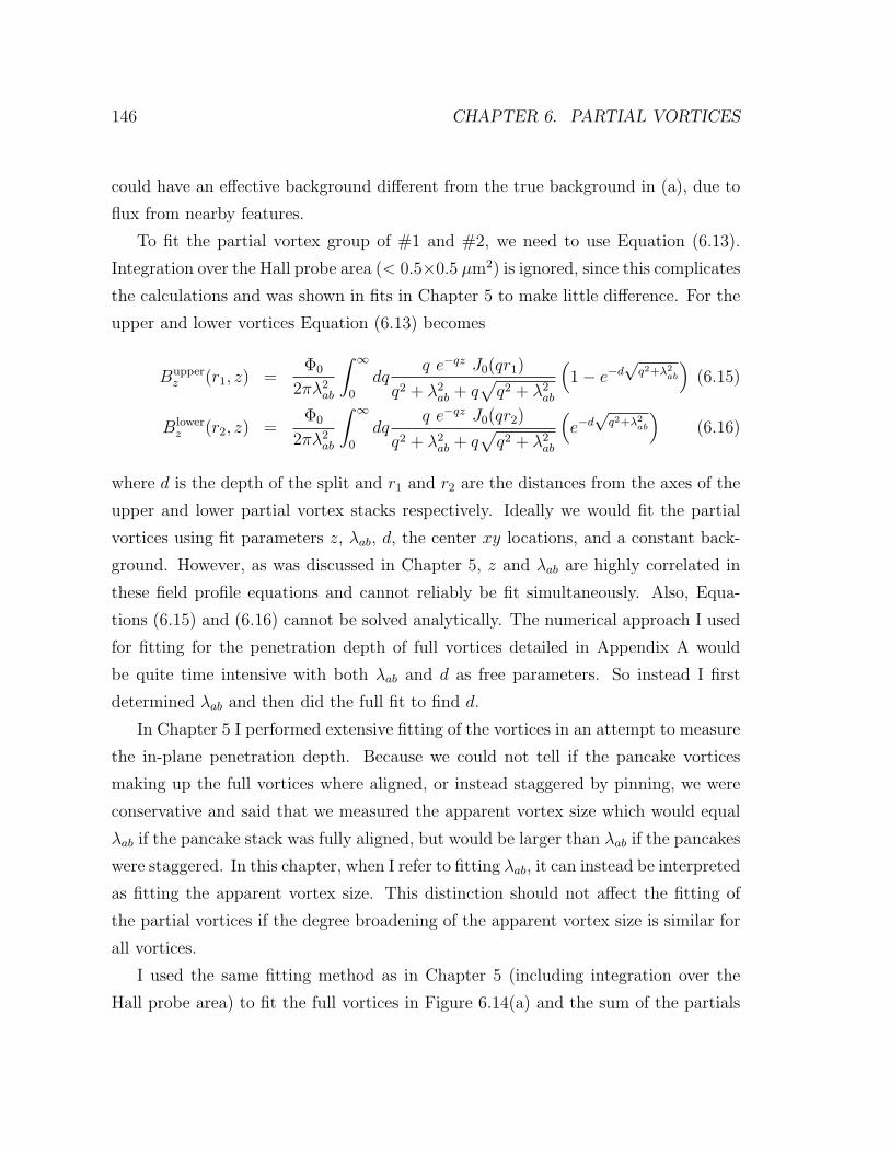
146 CHAPTER 6. PARTIAL VORTICES
could have an effective background different from the true background in (a), due to
flux from nearby features.
To fit the partial vortex group of #1 and #2, we need to use Equation (6.13).
Integration over the Hall probe area (< 0.5×0.5 µm2) is ignored, since this complicates
the calculations and was shown in fits in Chapter 5 to make little difference. For the
upper and lower vortices Equation (6.13) becomes
Bupperz (r1, z) =
Φ0
2πλ2ab
∫ ∞
0
dqq e−qz J0(qr1)
q2 + λ2ab + q
√q2 + λ2
ab
(1− e−d
√q2+λ2
ab
)(6.15)
Blowerz (r2, z) =
Φ0
2πλ2ab
∫ ∞
0
dqq e−qz J0(qr2)
q2 + λ2ab + q
√q2 + λ2
ab
(e−d√
q2+λ2ab
)(6.16)
where d is the depth of the split and r1 and r2 are the distances from the axes of the
upper and lower partial vortex stacks respectively. Ideally we would fit the partial
vortices using fit parameters z, λab, d, the center xy locations, and a constant back-
ground. However, as was discussed in Chapter 5, z and λab are highly correlated in
these field profile equations and cannot reliably be fit simultaneously. Also, Equa-
tions (6.15) and (6.16) cannot be solved analytically. The numerical approach I used
for fitting for the penetration depth of full vortices detailed in Appendix A would
be quite time intensive with both λab and d as free parameters. So instead I first
determined λab and then did the full fit to find d.
In Chapter 5 I performed extensive fitting of the vortices in an attempt to measure
the in-plane penetration depth. Because we could not tell if the pancake vortices
making up the full vortices where aligned, or instead staggered by pinning, we were
conservative and said that we measured the apparent vortex size which would equal
λab if the pancake stack was fully aligned, but would be larger than λab if the pancakes
were staggered. In this chapter, when I refer to fitting λab, it can instead be interpreted
as fitting the apparent vortex size. This distinction should not affect the fitting of
the partial vortices if the degree broadening of the apparent vortex size is similar for
all vortices.
I used the same fitting method as in Chapter 5 (including integration over the
Hall probe area) to fit the full vortices in Figure 6.14(a) and the sum of the partials
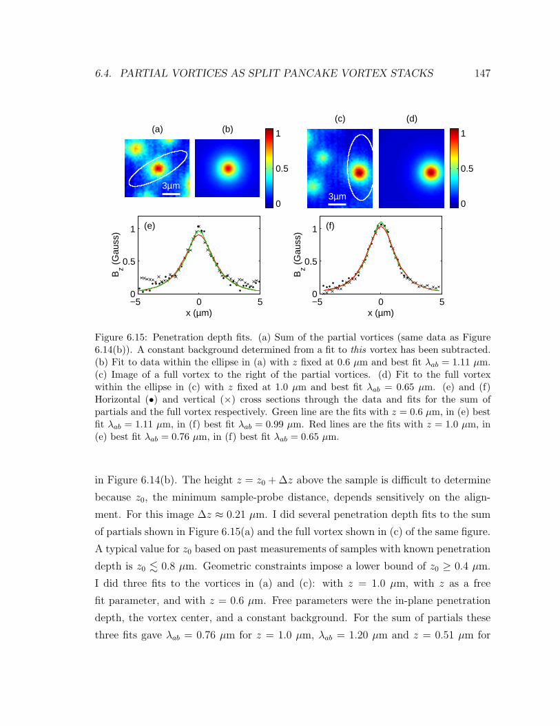
6.4. PARTIAL VORTICES AS SPLIT PANCAKE VORTEX STACKS 147
0
0.5
1
0
0.5
1 (a)
3µm
(b)
−5 0 50
0.5
1
x (µm)
Bz (
Gau
ss)
(e)
(c)
3µm
(d)
−5 0 50
0.5
1
x (µm)
Bz (
Gau
ss)
(f)
Figure 6.15: Penetration depth fits. (a) Sum of the partial vortices (same data as Figure6.14(b)). A constant background determined from a fit to this vortex has been subtracted.(b) Fit to data within the ellipse in (a) with z fixed at 0.6 µm and best fit λab = 1.11 µm.(c) Image of a full vortex to the right of the partial vortices. (d) Fit to the full vortexwithin the ellipse in (c) with z fixed at 1.0 µm and best fit λab = 0.65 µm. (e) and (f)Horizontal (•) and vertical (×) cross sections through the data and fits for the sum ofpartials and the full vortex respectively. Green line are the fits with z = 0.6 µm, in (e) bestfit λab = 1.11 µm, in (f) best fit λab = 0.99 µm. Red lines are the fits with z = 1.0 µm, in(e) best fit λab = 0.76 µm, in (f) best fit λab = 0.65 µm.
in Figure 6.14(b). The height z = z0 + ∆z above the sample is difficult to determine
because z0, the minimum sample-probe distance, depends sensitively on the align-
ment. For this image ∆z ≈ 0.21 µm. I did several penetration depth fits to the sum
of partials shown in Figure 6.15(a) and the full vortex shown in (c) of the same figure.
A typical value for z0 based on past measurements of samples with known penetration
depth is z0 . 0.8 µm. Geometric constraints impose a lower bound of z0 ≥ 0.4 µm.
I did three fits to the vortices in (a) and (c): with z = 1.0 µm, with z as a free
fit parameter, and with z = 0.6 µm. Free parameters were the in-plane penetration
depth, the vortex center, and a constant background. For the sum of partials these
three fits gave λab = 0.76 µm for z = 1.0 µm, λab = 1.20 µm and z = 0.51 µm for
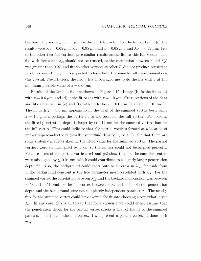
148 CHAPTER 6. PARTIAL VORTICES
the free z fit, and λab = 1.11 µm for the z = 0.6 µm fit. For the full vortex in (c) the
results were λab = 0.65 µm, λab = 0.95 µm and z = 0.65 µm, and λab = 0.99 µm. Fits
to the other two full vortices gave similar results as the fits to this full vortex. The
fits with free z and λab should not be trusted, as the correlation between z and λ−1ab
was greater than 0.97, and fits to other vortices at other Tc did not produce consistent
z0 values, even though z0 is expected to have been the same for all measurements on
this crystal. Nevertheless, the free z fits encouraged me to do the fits with z at the
minimum possible value of z = 0.6 µm.
Results of the lambda fits are shown in Figure 6.15. Image (b) is the fit to (a)
with z = 0.6 µm, and (d) is the fit to (c) with z = 1.0 µm. Cross sections of the data
and fits are shown in (e) and (f) with both the z = 0.6 µm fit and z = 1.0 µm fit.
The fit with z = 0.6 µm appears to fit the peak of the summed vortex best, while
z = 1.0 µm is perhaps the better fit to the peak for the full vortex. For fixed z,
the fitted penetration depth is larger by ≈ 0.12 µm for the summed vortex than for
the full vortex. This could indicate that the partial vortices formed at a location of
weaker superconductivity (smaller superfluid density ns ∝ λ−2). Or that there are
some systematic effects skewing the fitted value for the summed vortex. The partial
vortices were summed pixel by pixel, so the centers could not be aligned perfectly.
Fitted centers of the partial vortices #1 and #2 show that for the sum the centers
were misaligned by ≤ 0.04 µm, which could contribute to a slightly larger penetration
depth fit. Also, the background could contribute to an error in λab, for aside from
z, the background constant is the free parameter most correlated with λab. For the
summed vortex the correlation between λ−1ab and the background constant was between
-0.53 and -0.57, and for the full vortex between -0.39 and -0.46. So the penetration
depth and the background were not completely independent parameters. The nearby
flux for the summed vortex could have skewed the fit into choosing a somewhat larger
λab. In any case, this is all to say that for a chosen z we could either assume that
the penetration depth for the partial vortex stacks is that of the fit to the summed
partials, or is that of the full vortex. I will present a partial vortex fit done both
ways.
6.4. PARTIAL VORTICES AS SPLIT PANCAKE VORTEX STACKS 149
I fit the partial vortices #1 and #2 from Figure 6.13(a) simultaneously to Equa-
tions (6.15) and (6.16). Fixed parameters in the fit were z and λab, while free fit
parameters were the splitting depth d, the center locations of both partial vortices,
and a constant background. The fitting method is similar to that described in Ap-
pendix A.2. I performed the fit twice. Once with z = 0.6 µm and λab = 1.11 µm,
which are the values for the better-looking penetration depth fit to the summed
vortex in Figure 6.15. The fit with these input parameters gave splitting depth
d = 0.53 µm = 0.48λab. The second fit was with z = 1.0 µm and λab = 0.64 µm,
where are approximately the best looking fit values for the full vortex. This fit to
the partials gave d = 0.36 µm = 0.56λab. The fitting results are shown in Figure
6.16. Both fits do a good job of modelling the data. Further trials over an array of z
and λab might produce even better fits. However, the goal here of showing that the
partial vortices are indeed described by a split stack has been accomplished, and an
approximate split depth of 0.5λab for this partial vortex group has been determined.
It is clear from the fitting that the partial vortices can be modelled very well as split
stacks of pancake vortices.
This partial vortex pair was ideal for fitting because there were only two of them
and they were well defined. In many of the other images shown earlier in this chapter,
split stack modelling would be more complicated. Modelling becomes more difficult
when there are several splits of a single stack and when several groups of partial
vortices are nearby making it difficult to determine which partial belongs to which
group. Some partials appear elongated or have tails which could be the result of many
nearby splits that are unresolved by the Hall probe, or possibly tilts of a pancake stack.
6.4.4 Discussion
The explanation of the partial vortices as split stacks (with one or more splits)
is logical for these very underdoped YBa2Cu3O6+x crystals because the anisotropy
factor is very large (γ = λc/λab > 40). High anisotropy means that the Josephson
coupling between the layers is very weak so the coupling of pancake vortices is almost
only due to magnetic coupling, making it easier to separate them laterally. With no
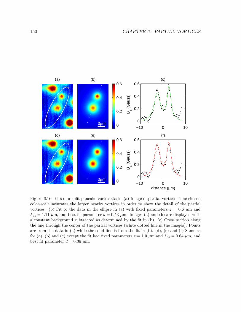
150 CHAPTER 6. PARTIAL VORTICES
(a)
0
0.2
0.4
0.6(b)
3µm−10 0 10
0
0.2
0.4
0.6
Bz (
Gau
ss)
(c)
(d)
0
0.2
0.4
0.6(e)
3µm−10 0 10
0
0.2
0.4
0.6
distance (µm)
Bz (
Gau
ss)
(f)
Figure 6.16: Fits of a split pancake vortex stack. (a) Image of partial vortices. The chosencolor-scale saturates the larger nearby vortices in order to show the detail of the partialvortices. (b) Fit to the data in the ellipse in (a) with fixed parameters z = 0.6 µm andλab = 1.11 µm, and best fit parameter d = 0.53 µm. Images (a) and (b) are displayed witha constant background subtracted as determined by the fit in (b). (c) Cross section alongthe line through the center of the partial vortices (white dotted line in the images). Pointsare from the data in (a) while the solid line is from the fit in (b). (d), (e) and (f) Same asfor (a), (b) and (c) except the fit had fixed parameters z = 1.0 µm and λab = 0.64 µm, andbest fit parameter d = 0.36 µm.
6.4. PARTIAL VORTICES AS SPLIT PANCAKE VORTEX STACKS 151
pinning, the magnetic coupling would align the pancake vortices in a straight stack, as
shown in Clem (1991). However, we know that there are pinning sites in the crystal,
since at the low flux densities we study the vortices remain in the sample after the
field is turned off at T < Tc.
From the energy calculations of Benkraouda and Clem (1996) mentioned earlier for
a tilted versus a kinked structure, it seems logical that given an appropriate pinning
landscape, split stack vortices would form in our crystals especially for the lowest
Tc’s in which the anisotropy should be largest. Thus pinning sites in the crystal are
important in the formation of partial vortices. It cannot be determined from our
images what the pinning sites are. They could be regions of oxygen inhomogeneity,
twinning boundaries, lattice imperfections or something else. Future studies of the
pinning landscape in these crystals and in other cuprates is desirable.
Above in Section 6.4.3 I showed that the model of a split pancake vortex stack fits
very well to the data. The split stack (with ≥1 splits) is also consistent with and can
explain the many properties of the partial vortices discussed earlier in Section 6.2.1.
I will now review these properties in light of the split stack explanation.
Partial vortices were more prevalent for the lowest Tc values. Anisotropy increases
as doping decreases, so the energy cost of the interlayer Josephson vortex in the split
is smaller for lower Tc, making a split stack more favorable. It might also be that
more pinning sites are present for low carrier doping. Another feature of the partial
vortices was that they carried a continuous range of flux, not just small fractions of
Φ0. This makes sense with the split stack since the flux through the top surface due
to a partial stack can have any value from 0 to Φ0 depending only on the depth of
the splitting as shown by Equation (6.14).3
Four other properties can also be explained in light of the split stack scenario.
Partial vortices were observed in groups that together carried a total flux of Φ0 within
a (relatively large) experimental error. This observation agrees beautifully with the
split pancake stack idea, because at each split a new partial stack begins. The sum
of the flux from all the partial stacks must be Φ0 for a group of pancake vortices
3Actually, the allowed splitting depths are discrete on the scale of the layer spacing s = 11.7 A,but since s ¿ λab the depth and the flux are continuous for all practical purposes.
152 CHAPTER 6. PARTIAL VORTICES
extending through the whole thickness of the sample with one pancake vortex per
layer. Partial vortices were observed to prefer certain regions of the sample, even
after a room temperature anneal. This could be explained if those regions had more
pinning sites (of whatever sort) that were favorable for partial vortices. It was also
observed that for Tc ∼ 14 K, where partial vortices were scarce, they could be created
by cooling the sample in a predominantly in-plane applied field. This is explained
nicely by the split stack model because if the flux lines are tilted during field cooling,
particularly above the angle determined by the calculations of Benkraouda and Clem
(1996), pancake vortices are much more likely to get pinned at an angle with respect
to others in the stack. Lastly, the partial vortices were observed to be more mobile
than full vortices. This makes sense due to the restoring forces on a split stack that
favor a straight unsplit stack: the attractive magnetic coupling between pancakes in
different layers, and the energy cost of the Josephson vortex linking the pancakes at
a split (weak for large anisotropy). A full vortex straight stack does not experience
these forces competing with pinning.
6.5 Summary
In this chapter I presented scanning SQUID and scanning Hall probe images of
features which looked like vortices with sub-Φ0 magnetic flux. This was surprising,
since flux should be quantized in a superconductor. The samples were single crystals
of very underdoped YBa2Cu3O6+x. Partial vortices were seen only in samples with
very low Tc and the probability of occurrence decreased with increasing Tc.
I showed that the observed partial vortices are the result of pancake vortex stacks
which split at one or more depths below the sample surface. Fluxoid quantization is
not violated. Modelling and fits show that a split stack does describe the data quite
well, and qualitatively all the properties of the partial vortices can be explained by
this model. For example the features appear in groups, can be formed by cooling
in a horizontal applied field, and are more mobile than full vortices. Split stacks of
pancake vortices can only occur in quasi-2D superconductors with large anisotropy
because the Josephson coupling between the superconducting layers must be small. It
6.5. SUMMARY 153
is not clear from these data if the large anisotropy alone is enough favor the split stack,
or if the observation of these features depends on inhomogeneities in the sample. To
our knowledge, these are the first observations of naturally occurring prevalent split
pancake vortices.

154 CHAPTER 6. PARTIAL VORTICES
Chapter 7
Conclusions
For this dissertation, I successfully implemented a cryogenic to room temperature
scanning magnetic microscope in an Oxford Instruments SXM system. I used both
Hall probes and Superconducting QUantum Interference Devices (SQUIDs) as the
scanning magnetic sensor, though my focus was on scanning Hall probe microscopy
(SHPM) due to its better spatial resolution and broad operating temperature range.
The microscope had a specially made piezoelectric scanner in an “S-bender” design
(Siegel et al. 1995) which allowed areas as large as 60 × 60 µm2 to be imaged at
4 K. I measured the lowest resonant frequency of this large area scanner to be
∼40 Hz (at room temperature) which is safely above the scan frequency chosen to
optimize the Hall probe imaging (.1 Hz). Along with the SXM, we also purchased
scanning electronics and software from Oxford, though I ended up implementing my
own separate data acquisition scheme with my own MABLAB r© code to circumvent
some grounding issues when the Hall probe was hooked up to the original hardware.
I spent part of my time fabricating and studying noise characteristics of submi-
cron scanning Hall probes. Hall probes are appealing magnetic sensors for scanning
microscopy because they have good sensitivity to magnetic field and flux, can be
fabricated down to at least the 100 nm length scale for submicron – and ultimately
nanoscale – spatial resolution, operate over a wide temperature and field range, and
their output is directly related to the magnetic field in the active area which makes
SHPM images relatively easy to interpret. Currently the best known materials for
scanning Hall probes at low temperature are GaAs/AlGaAs heterostructures which
155
156 CHAPTER 7. CONCLUSIONS
have a two-dimensional electron gas (2DEG) below the surface. The GaAs/AlGaAs
2DEG can be made with very low carrier densities and very high mobilities, mak-
ing it a good material for low noise Hall probes. I fabricated Hall probes from a
GaAs/AlGaAs structure with a 140 nm deep 2DEG (grown by David Kisker at IBM),
with probe dimensions from 0.5 µm to 2 µm. I included an extra process step to put
a thin metal gate over the active area to screen out electric fields from stray charges
which had previously been disturbing our magnetic imaging. The grounded gate
proved to be very helpful in improving the image quality.
The dominant noise in the smaller Hall probes was telegraph noise from one or
more “switching” states, which may be due to motion of remote dopants or impuri-
ties. Higher spatial resolution Hall probes are desirable for imaging many magnetic
systems, but if better spatial resolution comes with a loss of sensitivity, a compromise
would need to be made. We wanted to see how the sensitivity of a Hall probe scaled
with probe size, so we studied probes ranging in size from 130 nm to 10 µm, from my
fabricated probes and a later generation of probes made by Clifford Hicks on a 2DEG
structure grown by Hadas Shtrikman. Frequency spectra of the noise density in these
probes showed that field sensitivity worsened as probe size got smaller, but the flux
sensitivity improved with decreasing Hall probe size. For imaging small magnetic
features, flux sensitivity is the more relevant concern, so these studies showed that
probes down to the 100 nm scale can be made without sacrificing sensitivity. Our
best demonstrated flux sensitivity was for the 130 nm probe which had 16 µΦ0/√
Hz
for >1 kHz and 1 mΦ0/√
Hz for 0.1 Hz. The high frequency flux noise density is only
a factor of 10 larger than the flux sensitivity of scanning SQUIDs, and arises mainly
from the white noise of the room temperature preamplifier. The low frequency noise
is dominated by resistive noise which shows up as telegraph noise in the time domain.
I primarily used the SHPM to image magnetic vortices in superconductors, in
particular c-axis vortices in very underdoped crystals of YBa2Cu3O6+x. Observable
vortex properties, such as flux quantization and the extent of the vortex magnetic
field (determined by the penetration depth of the superconductor), give information
on the superconducting properties. This is especially useful in the cuprate supercon-
ductors where the mechanism of superconductivity is not yet understood. The very
157
underdoped regime is of particular importance because the superfluid density is very
low and strong theoretical predictions have been made.
The vortex imaging experiments in this dissertation were made possible in part by
the recent developments in YBa2Cu3O6+x (YBCO) crystal growth and preparation
(Liang et al. 1998, 2002) extending to the very underdoped region with x ≈ 0.35 and
Tc in the range 4–20 K. After growth and a high temperature anneal, the degree
of oxygen ordering in the CuO chains increases with room temperature annealing,
taking the crystal from non-superconducting up to a saturation Tc after several weeks
at room temperature. This Tc change with room temperature annealing was exploited
in Chapters 5 and 6 of this dissertation to study vortex properties for a range of Tc
values (5–15 K) on the same sample. The very underdoped samples can have narrow
transition widths (typically ∆Tc < 2 K) as measured with magnetic susceptibility,
which can be interpreted to mean the samples are highly homogeneous. However,
my images at the lowest Tc values (. 10 K) show inhomogeneity of the vortex field
profiles which may imply doping inhomogeneities for these lowest Tc samples.
My first magnetic imaging experiments in the very underdoped YBCO were done
to test a scenario of spin-charge separation (SCS) proposed as the mechanism for
cuprate superconductivity. In SCS, the electron fractionalizes into a spin-1/2, charge
zero, spinon and a spin-0, charge e, chargon. The chargons could, in principle, con-
dense directly to the superconducting state without needing to form Cooper pairs.
Senthil and Fisher (2000) formulated a microscopic SCS theory for the cuprates which
included an excitation – or topological defect in a Z2 gauge field – called a vison. We
tested this promising theory for cuprate superconductivity by looking for experimen-
tal signatures of the vison. The Senthil-Fisher scenario allows flux to be quantized as
hc/2e because any hc/2e vortices would be accompanied by a vison which provides
the additional π phase winding required to keep the superconducting wave function of
the chargon condensate single-valued. For very low Tc, it is predicted that hc/e vor-
tices would be energetically preferred (Senthil and Fisher 2001a). With the scanning
microscope we imaged vortices in four crystals of very underdoped YBCO, but never
saw hc/e vortices. This set an upper bound on the vison energy of Evison/kB < 60 K,
which is much below the predicted energy Evison ≈ kBT ∗ (Senthil and Fisher 2001a).
158 CHAPTER 7. CONCLUSIONS
We also performed a more stringent test for visons by looking for a “vortex mem-
ory” effect in small rings fabricated from the YBCO crystals. In this experiment an
odd or even number of hc/2e flux quanta are trapped in the hole of the ring. If the
temperature of the ring is warmed in zero field just above Tc, the flux will escape,
but if the original state of the ring contained an odd number of flux quanta, a vison
will be in the hole. If the sample is recooled below Tc before the vison can escape,
an hc/2e flux quantum of either sign must appear in the hole. We performed the
vortex memory experiment on four samples and never saw signatures of the vison.
This experiment addressed the dynamical properties of the vison and set an upper
bound of Evison/kB < 190 K ¿ T ∗. Together these experiments rule out scenarios of
SCS in the cuprates which require visons.
In another set of experiments, I attempted to measure the in-plane penetration
depth in a very underdoped YBa2Cu3O6.375 crystal as a function of Tc (which increased
with room temperature annealing). The extent of the vortex flux in the bulk of the
superconductor is given by λab and determines the shape of the field profile imaged at
the sample surface with the Hall probe. A difficulty with this method of determining
the penetration depth is the uncertainty about other possible contributions to the
vortex size. These very underdoped samples have large anisotropy, and thus it cannot
be ruled out that the 2D pancake vortices which compose the observed 3D vortices
are not pinned in a staggered fashion from layer to layer, which would increase the
apparent extent sab of the vortex. By fitting the observed vortex field profiles I was
able to measure sab which is an upper limit on λab. If sab is the same as λab, then
my results give penetration depths (related to the superfluid density ns/m∗) which
are larger than predicted by the universal Uemura relation (Uemura et al. 1989)
Tc ∝ λ(0)−2 ∝ ns(0)/m∗. The Uemura relation was found for underdoped samples,
but had not been tested in the extremely underdoped regime. Emery and Kivelson
(1995a) explained the Uemura relation as thermal phase fluctuations destroying the
superconductivity and setting Tc for underdoped samples. If my measurements are
reflective of the true λab, then modification of the theory will be needed to explain
these results.
Finally, in the very low Tc YBCO crystals, I observed what appeared to be partial
159
vortices (i.e. flux bundles smaller than hc/2e). I studied the properties of these
features and found they are more mobile than “full” vortices, tend to occur in groups,
and their frequency of occurrence could be increased by field cooling the sample in a
field with a large horizontal component. All these properties suggest that the partial
vortices are the result of a full vortex that was partially displaced laterally. This can
occur in highly anisotropic layered superconductors where a vortex is appropriately
modelled as a stack of 2D pancake vortices (Clem 1991; Benkraouda and Clem 1996).
The observed partial vortices are interpreted to be the field from partial stacks of
pancake vortices displaced by some horizontal distance. My data show displacements
as large as tens-of-microns. I computed the fields for a stack with one split, and fit
this model to an observed pair of partial vortices with the depth of the stack splitting
as a free parameter. The model fit the data quite well. A continuum of split depths
and a varying total number of splits (per full vortex) were observed in the data. To
my knowledge, these are the first observations of naturally occurring prevalent split
pancake vortices. (A split stack was observed once by Grigorenko et al. (2002). It
was created by an abrupt change in the external field, and was atypical.) The data
qualitatively give information about the crystal anisotropy and pinning landscapes,
though it is not yet clear what role, if any, inhomogeneities in the sample play in
forming the partial vortices.
In summary, scanning Hall probe microscopy is a useful tool for studying magnetic
samples. SHPM has submicron spatial resolution and the probes can be made as small
as ∼100 nm without compromising flux sensitivity. I fabricated submicron probes and
used them in a variable temperature scanning probe microscope to study vortices in
newly available very underdoped YBa2Cu3O6+x single crystals. These studies refuted
a promising theory for cuprate superconductivity, measured the apparent extent of
the vortex field in these crystals, and revealed a prevalent phenomena of split vortices.
Further studies of these and other cuprate superconductors with scanning magnetic
microscopy and other techniques will hopefully help determine the elusive mechanism
of high-temperature superconductivity.
160 CHAPTER 7. CONCLUSIONS
Appendix A
Details of the model for vortex fitting
Fits to individual magnetic vortices in a superconductor were performed at many
stages of this dissertation, most particularly for the penetration depth measurements
discussed in Chapter 5. In all cases the YBa2Cu3O6+x samples had the ab-plane
parallel to the surface and the imaged vortices were along the c-axis. Obviously a
model is required if we want to fit the vortices. Parameters such as the in-plane
penetration depth (λab) and/or the total flux carried by the vortex (Φ, which in this
Appendix will be treated as a fixed parameter Φ = Φ0) can be obtained from fits.
Here I review the model for the magnetic field profile of a vortex and give details
on integrating over the Hall probe area. The fitting was done with the non-linear
regression routine in Mathematica r©, so the model had to be put in a differentiable
form.
Take a c-axis vortex in a crystal with axial symmetry (λa = λb) where the sample
surface is parallel to the ab and xy planes. The magnetic field profile of the vortex
can be found from London’s equations and Maxwell’s equations (Pearl 1966; Kogan
et al. 1993; Kirtley et al. 1999a). The z component of the magnetic field above an
infinite plane superconductor due to a c-axis vortex is
Bz(r, z) =Φ0
(2πλab)2
∫d2q eiq·r e−qz
Q[Q + q coth(Qd/2)], (A.1)
where d is the thickness of the superconductor, r = (x, y) is the radial distance from
the vortex center, q = (qx, qy), Q =√
q2 + λ−2ab , and z is the distance above the
161
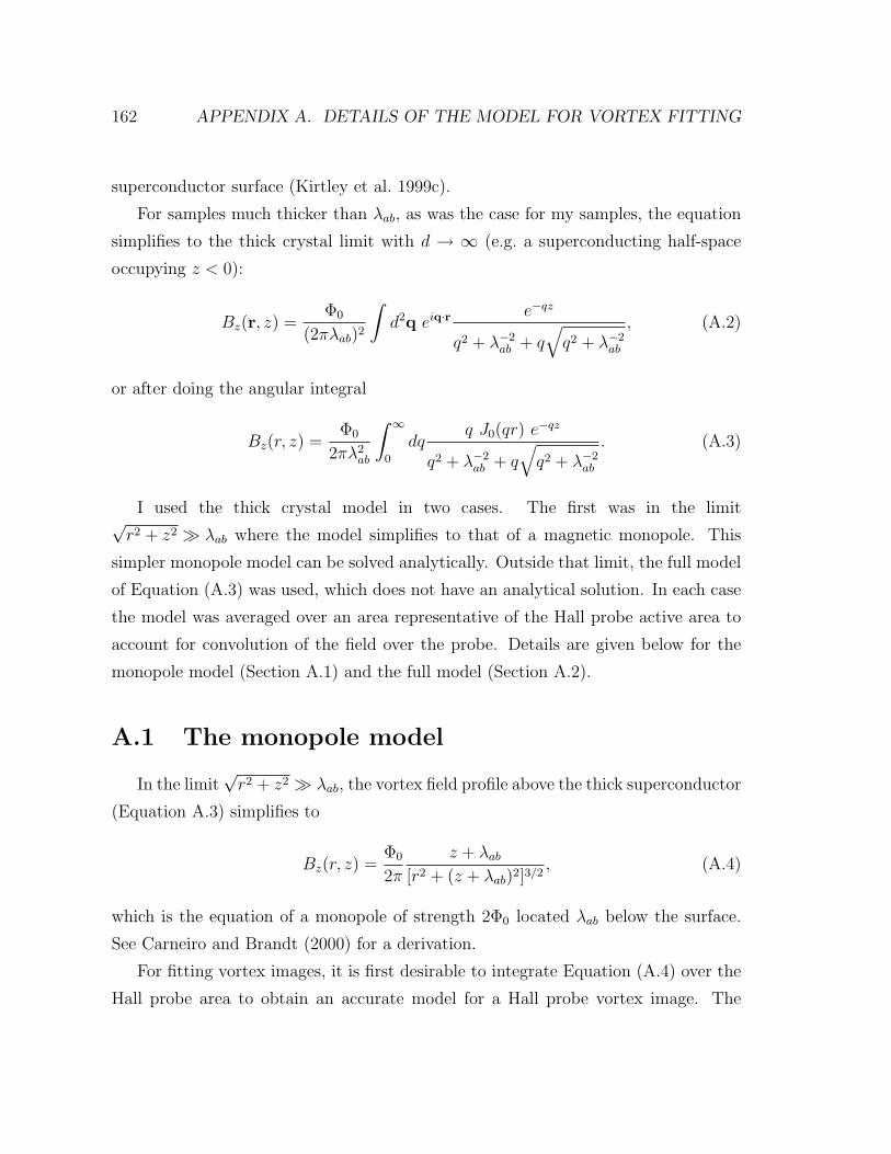
162 APPENDIX A. DETAILS OF THE MODEL FOR VORTEX FITTING
superconductor surface (Kirtley et al. 1999c).
For samples much thicker than λab, as was the case for my samples, the equation
simplifies to the thick crystal limit with d → ∞ (e.g. a superconducting half-space
occupying z < 0):
Bz(r, z) =Φ0
(2πλab)2
∫d2q eiq·r e−qz
q2 + λ−2ab + q
√q2 + λ−2
ab
, (A.2)
or after doing the angular integral
Bz(r, z) =Φ0
2πλ2ab
∫ ∞
0
dqq J0(qr) e−qz
q2 + λ−2ab + q
√q2 + λ−2
ab
. (A.3)
I used the thick crystal model in two cases. The first was in the limit√r2 + z2 À λab where the model simplifies to that of a magnetic monopole. This
simpler monopole model can be solved analytically. Outside that limit, the full model
of Equation (A.3) was used, which does not have an analytical solution. In each case
the model was averaged over an area representative of the Hall probe active area to
account for convolution of the field over the probe. Details are given below for the
monopole model (Section A.1) and the full model (Section A.2).
A.1 The monopole model
In the limit√
r2 + z2 À λab, the vortex field profile above the thick superconductor
(Equation A.3) simplifies to
Bz(r, z) =Φ0
2π
z + λab
[r2 + (z + λab)2]3/2, (A.4)
which is the equation of a monopole of strength 2Φ0 located λab below the surface.
See Carneiro and Brandt (2000) for a derivation.
For fitting vortex images, it is first desirable to integrate Equation (A.4) over the
Hall probe area to obtain an accurate model for a Hall probe vortex image. The
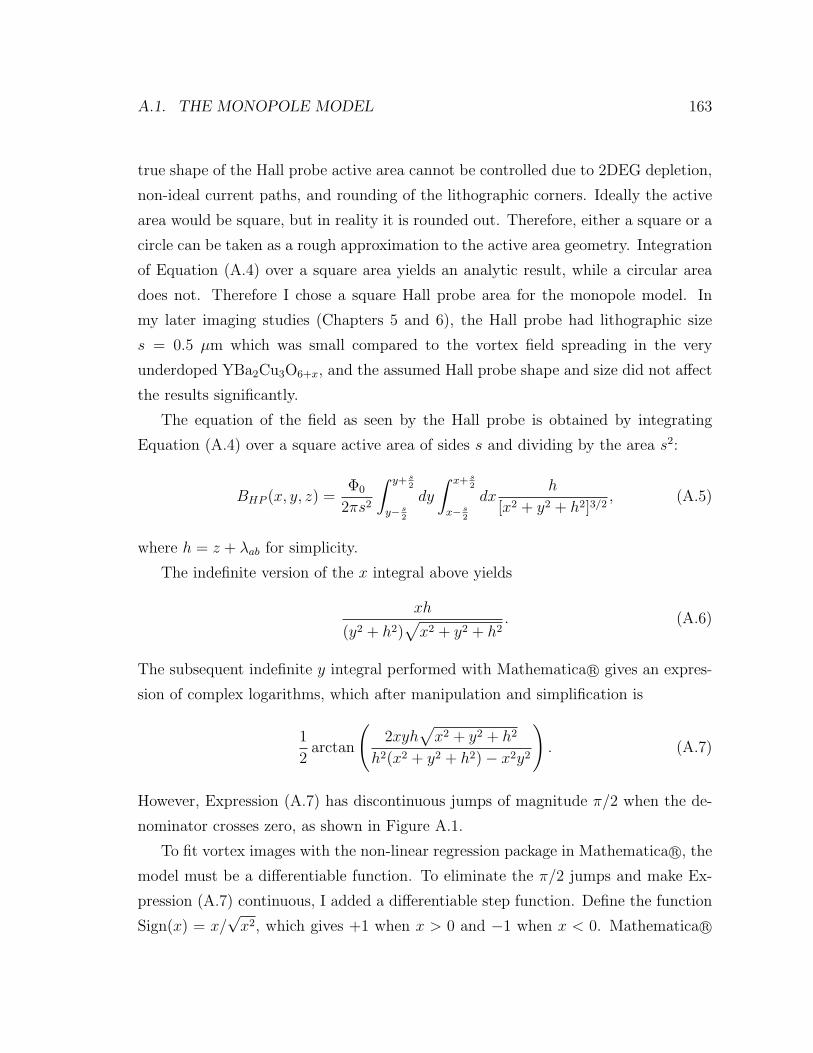
A.1. THE MONOPOLE MODEL 163
true shape of the Hall probe active area cannot be controlled due to 2DEG depletion,
non-ideal current paths, and rounding of the lithographic corners. Ideally the active
area would be square, but in reality it is rounded out. Therefore, either a square or a
circle can be taken as a rough approximation to the active area geometry. Integration
of Equation (A.4) over a square area yields an analytic result, while a circular area
does not. Therefore I chose a square Hall probe area for the monopole model. In
my later imaging studies (Chapters 5 and 6), the Hall probe had lithographic size
s = 0.5 µm which was small compared to the vortex field spreading in the very
underdoped YBa2Cu3O6+x, and the assumed Hall probe shape and size did not affect
the results significantly.
The equation of the field as seen by the Hall probe is obtained by integrating
Equation (A.4) over a square active area of sides s and dividing by the area s2:
BHP (x, y, z) =Φ0
2πs2
∫ y+ s2
y− s2
dy
∫ x+ s2
x− s2
dxh
[x2 + y2 + h2]3/2, (A.5)
where h = z + λab for simplicity.
The indefinite version of the x integral above yields
xh
(y2 + h2)√
x2 + y2 + h2. (A.6)
The subsequent indefinite y integral performed with Mathematica r© gives an expres-
sion of complex logarithms, which after manipulation and simplification is
1
2arctan
(2xyh
√x2 + y2 + h2
h2(x2 + y2 + h2)− x2y2
). (A.7)
However, Expression (A.7) has discontinuous jumps of magnitude π/2 when the de-
nominator crosses zero, as shown in Figure A.1.
To fit vortex images with the non-linear regression package in Mathematica r©, the
model must be a differentiable function. To eliminate the π/2 jumps and make Ex-
pression (A.7) continuous, I added a differentiable step function. Define the function
Sign(x) = x/√
x2, which gives +1 when x > 0 and −1 when x < 0. Mathematica r©
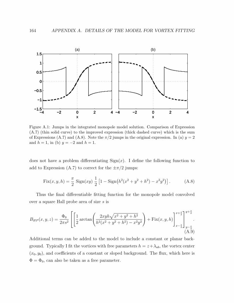
164 APPENDIX A. DETAILS OF THE MODEL FOR VORTEX FITTING
−4 −2 0 2 4−1.5
−1
−0.5
0
0.5
1
1.5
−4 −2 0 2 4−4 −2 0 2 4−1.5
−1
−0.5
0
0.5
1
1.5
x−4 −2 0 2 4
x−4 −2 0 2 4
−1.5
−1
−0.5
0
0.5
1
1.5
x
(a)
−4 −2 0 2 4x
(b)
Figure A.1: Jumps in the integrated monopole model solution. Comparison of Expression(A.7) (thin solid curve) to the improved expression (thick dashed curve) which is the sumof Expressions (A.7) and (A.8). Note the π/2 jumps in the original expression. In (a) y = 2and h = 1, in (b) y = −2 and h = 1.
does not have a problem differentiating Sign(x). I define the following function to
add to Expression (A.7) to correct for the ±π/2 jumps:
Fix(x, y, h) =π
2Sign(xy)
1
2
[1− Sign
(h2(x2 + y2 + h2)− x2y2
)]. (A.8)
Thus the final differentiable fitting function for the monopole model convolved
over a square Hall probe area of size s is
BHP (x, y, z) =Φ0
2πs2
[1
2arctan
(2xyh
√x2 + y2 + h2
h2(x2 + y2 + h2)− x2y2
)+ Fix(x, y, h)
]x+ s2
x− s2
y+ s2
y− s2
.
(A.9)
Additional terms can be added to the model to include a constant or planar back-
ground. Typically I fit the vortices with free parameters h = z+λab, the vortex center
(x0, y0), and coefficients of a constant or sloped background. The flux, which here is
Φ = Φ0, can also be taken as a free parameter.
A.2. THE FULL MODEL 165
A.2 The full model
When the penetration depth λab is not small compared to the distance from the
vortex, the full model given in Equation (A.3) must be used. This integral cannot be
solved analytically. Instead we integrate it numerically in Mathematica r© and then
create an interpolated function. The interpolated function can either be used directly
in fitting the vortex image if the Hall probe size is small compared to the feature size,
or it can first be numerically integrated over an area representing the Hall probe.1
Equation (A.3) for the vortex field can also be written as
Bz(r, z) =Φ0
2πλ2ab
∫ ∞
0
dqq J0(qr) e−qz
q2 + 1 + q√
q2 + 1. (A.10)
where r = r/λab, z = z/λab, and q = qλab are dimensionless. In this way the
integral is now only a function of two unknowns, r and z, since explicit reference
to λab has been eliminated. This integral was numerically integrated for a grid of
11,799 values of (r, z) ranging from 0–65 for r and 0.03–20.03 for z. Step size
ranged from 0.1–1.0 for ∆r and from 0.1–0.5 for ∆z, with increasing step sizes as
r and z increased, respectively. Integrating with the full 0 to ∞ limits worked for
some values of r and z by invoking the Mathematica r© “oscillatory” method, while
for other values it was necessary to truncate the integration with an upper limit of
q = 20/z. Due to the exponential e−qz term in the integrand, this is completely
sufficient. Finally, the 11,799 numerical integrations were converted to an interpo-
lated function in Mathematica r© which I will denote by Interp(r/λab, z/λab) such that
Bz(r, z) = (Φ0/2πλ2ab) Interp(r/λab, z/λab). The vortex images can be fit to this Bz
when convolution of the field over the Hall probe is not of concern.
For a further accurate model, I averaged Bz(r, z) over the area of the Hall probe. In
order to preserve the radial symmetry, a circular geometry with radius ρ was chosen for
the Hall probe area. As mentioned earlier, the actual Hall probe geometry is probably
between that of a square and a circle. Since the probe was small (ρ . 0.25 µm) for
1The full model numerical computations and data fitting discussed here were initially imple-mented by Hendrik Bluhm.
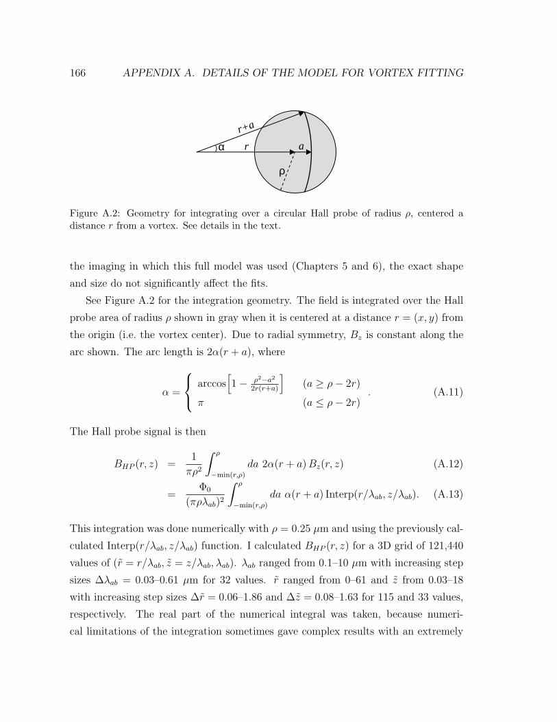
166 APPENDIX A. DETAILS OF THE MODEL FOR VORTEX FITTING
α r a
r+a
)
ρ
Figure A.2: Geometry for integrating over a circular Hall probe of radius ρ, centered adistance r from a vortex. See details in the text.
the imaging in which this full model was used (Chapters 5 and 6), the exact shape
and size do not significantly affect the fits.
See Figure A.2 for the integration geometry. The field is integrated over the Hall
probe area of radius ρ shown in gray when it is centered at a distance r = (x, y) from
the origin (i.e. the vortex center). Due to radial symmetry, Bz is constant along the
arc shown. The arc length is 2α(r + a), where
α =
arccos[1− ρ2−a2
2r(r+a)
](a ≥ ρ− 2r)
π (a ≤ ρ− 2r). (A.11)
The Hall probe signal is then
BHP (r, z) =1
πρ2
∫ ρ
−min(r,ρ)
da 2α(r + a) Bz(r, z) (A.12)
=Φ0
(πρλab)2
∫ ρ
−min(r,ρ)
da α(r + a) Interp(r/λab, z/λab). (A.13)
This integration was done numerically with ρ = 0.25 µm and using the previously cal-
culated Interp(r/λab, z/λab) function. I calculated BHP (r, z) for a 3D grid of 121,440
values of (r = r/λab, z = z/λab, λab). λab ranged from 0.1–10 µm with increasing step
sizes ∆λab = 0.03–0.61 µm for 32 values. r ranged from 0–61 and z from 0.03–18
with increasing step sizes ∆r = 0.06–1.86 and ∆z = 0.08–1.63 for 115 and 33 values,
respectively. The real part of the numerical integral was taken, because numeri-
cal limitations of the integration sometimes gave complex results with an extremely
A.2. THE FULL MODEL 167
small imaginary component. Finally the 121,440 values were interpolated to give the
function InterpHP(r/λab, z/λab, λab) which was specifically for ρ = 0.25 µm. This
interpolated solution for BHP (r, z) was then used as the fitting model for vortex im-
ages with non-linear regression. Terms for a constant background and a planar slope
(optional) were added to the model. Free parameters in the fit were λab, the vortex
center (x0, y0), and coefficients of a constant or sloped background. z was typically
chosen prior to the fit, because z and λab are highly correlated in the model and do
not give realistic results if both are fit independently (e.g. some attempts to fit data
with z and λab independently gave unphysical λab < 0 or z < 0.4 µm results).

168 APPENDIX A. DETAILS OF THE MODEL FOR VORTEX FITTING
List of References
H. Alloul, T. Ohno, and P. Mendels. 89Y NMR evidence for a Fermi-liquid behaviorin YBa2Cu3O6+x. Physical Review Letters 63, 1700–3 (1989).
P.W. Anderson. The resonating valence bond state in La2CuO4 and superconductiv-ity. Science 235, 1196–8 (1987).
D.N. Basov, R. Liang, D.A. Bonn, W.N. Hardy, B. Dabrowski, M. Quijada, D.B.Tanner, J.P. Rice, D.M. Ginsberg, and T. Timusk. In-plane anisotropy of thepenetration depth in YBa2Cu3O7−x and YBa2Cu4O8 superconductors. PhysicalReview Letters 74, 598–601 (1995).
M.R. Beasley, R. Labusch, and W.W. Webb. Flux creep in type-II superconductors.Physical Review 181, 682–700 (1969).
J.G. Bednorz and K.A. Muller. Possible high Tc superconductivity in the Ba-La-Cu-Osystem. Zeitschrift fur Physik B 64, 189–93 (1986).
S.J. Bending. Local magnetic probes of superconductors. Advances in Physics 48,449–535 (1999).
S.J. Bending and A. Oral. Hall effect in a highly inhomogeneous magnetic fielddistribution. Journal of Applied Physics 81, 3721–5 (1997).
M. Benkraouda and J.R. Clem. Instability of a tilted vortex line in magneticallycoupled layered superconductors. Physical Review B 53, 438–42 (1996).
J. Hendrik Bluhm. Private communication.
D.A. Bonn, S. Kamal, A. Bonakdarpour, Ruixing Liang, W.N. Hardy, C.C. Homes,D.N. Basov, and T. Timusk. Surface impedance studies of YBCO. CzechoslovakJournal of Physics 46, S6, 3195–202 (1996).
D.A. Bonn, J.C. Wynn, B.W. Gardner, Yu-Ju Lin, R. Liang, W.N. Hardy, J.R. Kirt-ley, and K.A. Moler. A limit on spin-charge separation in high-Tc superconductorsfrom the absence of a vortex-memory effect. Nature 414, 887–9 (2001).
169
170 LIST OF REFERENCES
G. Carneiro and E.H. Brandt. Vortex lines in films: Fields and interactions. PhysicalReview B 61, 6370–6 (2000).
A. Carrington, R.W. Giannetta, J.T. Kim, and J. Giapintzakis. Absence of nonlinearMeissner effect in YBa2Cu3O6.95. Physical Review B 59, R14173–6 (1999).
A.R. Champagne, A.J. Couture, F. Kuemmeth, and D.C. Ralph. Nanometer-scalescanning sensors fabricated using stencil lithography. Applied Physics Letters 82,1111–3 (2003).
A.M. Chang, H.D. Hallen, L. Harriott, H.F. Hess, H.L. Kao, J. Kwo, R.E. Miller,R. Wolfe, J. van der Ziel, and T.Y. Chang. Scanning Hall probe microscopy. AppliedPhysics Letters 61, 1974–6 (1992).
B.K. Chong, H. Zhou, G. Mills, L. Donaldson, and J.M.R. Weaver. Scanning Hallprobe microscopy on an atomic force microscope tip. Journal of Vacuum Science& Technology A 19, 1769–72 (2001).
C.-H. Chung, K. Voelker, and Y.B. Kim. Statistics of spinons in the spin-liquid phaseof Cs2CuCl4. Physical Review B 68, 94412/1–4 (2003).
J.R. Clem. Two-dimensional vortices in a stack of thin superconducting films: Amodel for high-temperature superconducting multilayers. Physical Review B 43,7837–46 (1991).
J.R. Clem. 2D pancake vortices in a finite stack of superconducting layers. PhysicaC 235–240, 2607–8 (1994).
R. Coldea, D.A. Tennant, A.M. Tsvelik, and Z. Tylczynski. Experimental realizationof a 2D fractional quantum spin liquid. Physical Review Letters 86, 1335–8 (2001).
D. Davidovic, S. Kumar, D.H. Reich, J. Siegel, S.B. Field, R.C. Tiberio, R. Hey, andK. Ploog. Correlations and disorder in arrays of magnetically coupled supercon-ducting rings. Physical Review Letters 76, 815–18 (1996).
Jr. Deaver, B.S. and W.M. Fairbank. Experimental evidence for quantized flux insuperconducting cylinders. Physical Review Letters 7, 43–6 (1961).
G.C. DeSalvo, W.F. Tseng, and J. Comas. Etch rates and selectivities of cit-ric acid/hydrogen peroxide on GaAs, Al0.3Ga0.7As, In0.2Ga0.8As, In0.53Ga0.47As,In0.52Al0.48As, and InP. Journal of the Electrochemical Society 139, 831–5 (1992).
V.J. Emery and S.A. Kivelson. Importance of phase fluctuations in superconductorswith small superfluid density. Nature 374, 434–7 (1995a).
LIST OF REFERENCES 171
V.J. Emery and S.A. Kivelson. Superconductivity in Bad Metals. Physical ReviewLetters 74, 3253–6 (1995b).
A.T. Fiory, A.F. Hebard, P.M. Mankiewich, and R.E. Howard. Penetration depthsof high Tc films measured by two-coil mutual inductances. Applied Physics Letters52, 2165–7 (1988).
C.J.B. Ford, S. Washburn, M. Buttiker, C.M. Knoedler, and J.M. Hong. Influence ofgeometry on the Hall effect in ballistic wires. Physical Review Letters 62, 2724–7(1989).
M. Franz and Z. Tesanovic. Flux tubes, visons, and vortices in spin-charge separatedsuperconductors. Physica C 357–60, 49–52 (2001).
T. Fukumura, H. Sugawara, K. Kitazawa, T. Hasegawa, Y. Nagamune, T. Noda,and H. Sakaki. Development of a scanning Hall probe microscope for simultaneousmagnetic and topographic imaging. Micron 30, 575–8 (1999).
B.W. Gardner, J.C. Wynn, P.G. Bjornsson, E.W.J. Straver, K.A. Moler, J.R. Kirt-ley, and M.B. Ketchen. Scanning superconducting quantum interference devicesusceptometry. Review of Scientific Instruments 72, 2361–4 (2001).
B.W. Gardner, J.C. Wynn, D.A. Bonn, Ruixing Liang, W.N. Hardy, J.R. Kirtley,V.G. Kogan, and K.A. Moler. Manipulation of single vortices in YBa2Cu3O6.354
with a locally applied magnetic field. Applied Physics Letters 80, 1010–2 (2002).
D. Goldhaber-Gordon, H. Shtrikman, D. Mahalu, D. Abusch-Magder, U. Meirav,and M.A. Kastner. Kondo effect in a single-electron transistor. Nature 391, 156–9(1998).
C.E. Gough, M.S. Colclough, E.M. Forgan, R.G. Jordan, M. Keene, C.M. Muirhead,A.I.M. Rae, N. Thomas, J.S. Abell, and S. Sutton. Flux quantization in a high-Tc
superconductor. Nature 326, 855 (1987).
A.N. Grigorenko, S.J. Bending, J.K. Gregory, and R.G. Humphreys. Scanning Hallprobe microscopy of flux penetration into a superconducting YBa2Cu3O7−δ thinfilm strip. Applied Physics Letters 78, 1586–8 (2001).
A.N. Grigorenko, S.J. Bending, A.E. Koshelev, J.R. Clem, T. Tamegai, and S. Ooi.Visualization of interacting crossing vortex lattices in the presence of quencheddisorder. Physical Review Letters 89, 217003/1–4 (2002).
V. Gusiatnikov, F. Altomare, J.C. Chen, A.M. Chang, A. Lichtenberger, andJ. Woodall. Nanoscale Scanning Hall Probe Microscopy. Bulletin of the Amer-ican Physical Society 46, 917 (2001).
172 LIST OF REFERENCES
E.H. Hall. On a new action of the magnet on electric currents. American Journal ofMathematices 2, 287–92 (1879).
W.N. Hardy, D.A. Bonn, D.C. Morgan, Ruixing Liang, and Kuan Zhang. Precisionmeasurements of the temperature dependence of lambda in YBa2Cu3O6.95: strongevidence for nodes in the gap function. Physical Review Letters 70, 3999–4002(1993).
K. Hasselbach, C. Veauvy, and D. Mailly. MicroSQUID magnetometry and magneticimaging. Physica C 332, 140–7 (2000).
Paul Horowitz and Winfield Hill. The Art of Electronics. Cambridge University Press,2nd ed. (1989).
A. Hosseini, D.M. Broun, D.E. Sheehy, T.P. Davis, M. Franz, W.N. Hardy, RuixingLiang, and D.A. Bonn. Survival of the d-wave superconducting state near theedge of antiferromagnetism in the cuprate phase diagram. xxx.lanl.gov cond-mat/0312542 (2003).
H.J. Hug, A. Moser, I. Parashikov, B. Stiefel, O. Fritz, H.-J. Gintherodt, andH. Thomas. Observation and manipulation of vortices in YBa2Cu3O7 thin filmwith a low temperature magnetic force microscope. Physica C 235-240, 2695–6(1994).
J.R. Kirtley. SQUID microscopy for fundamental studies. Physica C 368, 55–65(2002).
J.R. Kirtley, P. Chaudhari, M.B. Ketchen, N. Khare, Shawn-Yu Lin, and T. Shaw.Distribution of magnetic flux in high-Tc grain-boundary junctions enclosing hexag-onal and triangular areas. Physical Review B 51, 12057–60 (1995a).
J.R. Kirtley, M.B. Ketchen, K.G. Stawiasz, J.Z. Sun, W.J. Gallagher, S.H. Blanton,and S.J. Wind. High-resolution scanning SQUID microscope. Applied PhysicsLetters 66, 1138–40 (1995b).
J.R. Kirtley, V.G. Kogan, J.R. Clem, and K.A. Moler. Magnetic field of an in-planevortex outside a layered superconductor. Physical Review B 59, 4343–8 (1999a).
J.R. Kirtley, C.C. Tsuei, V.G. Kogan, J.R. Clem, H. Raffy, and Z.Z. Li. Fluxoiddynamics in superconducting thin film rings. Physical Review B 68, 214505/1–8(2003).
J.R. Kirtley, C.C. Tsuei, and K.A. Moler. Temperature dependence of the half-integermagnetic flux quantum. Science 285, 1373–5 (1999b).
LIST OF REFERENCES 173
J.R. Kirtley, C.C. Tsuei, K.A. Moler, V.G. Kogan, J.R. Clem, and A.J. Turberfield.Variable sample temperature scanning superconducting quantum interference de-vice microscope. Applied Physics Letters 74, 4011–3 (1999c).
J.R. Kirtley, C.C. Tsuei, H. Raffy, Z.Z. Li, V.G. Kogan, J.R. Clem, and K.A.Moler. Direct measurement of single fluxoid dynamics in superconducting rings.xxx.lanl.gov cond-mat/0103474 (2001).
J.R. Kirtley, C.C. Tsuei, M. Rupp, J.Z. Sun, L.S. Yu-Jahnes, A. Gupta, M.B.Ketchen, K.A. Moler, and M. Bhushan. Direct imaging of integer and half-integerJosephson vortices in high-Tc grain boundaries. Physical Review Letters 76, 1336–9(1996).
S.A. Kivelson. Personal communication.
S.A. Kivelson, D.S. Rokhsar, and J.P. Sethna. Topology of the resonating valence-bond state: solitons and high-Tc superconductivity. Physical Review B 35, 8865–8(1987).
S.A. Kivelson, D.S. Rokhsar, and J.P. Sethna. 2e or not 2e: flux quantization in theresonating valence bond state. Europhysics Letters 6, 353–8 (1988).
V.G. Kogan. Unpublished.
V.G. Kogan, A.Yu. Simonov, and M. Ledvij. Magnetic field of vortices crossing asuperconductor surface. Physical Review B 48, 392–7 (1993).
L. Krusin-Elbaum, R.L. Greene, F. Holtzberg, A.P. Malozemoff, and Y. Yeshurun.Direct measurement of the temperature-dependent magnetic penetration depth inY-Ba-Cu-O crystals. Physical Review Letters 62, 217–20 (1989).
C. Kurdak, C.-J. Chen, D.C. Tsui, S. Parihar, S. Lyon, and G.W. Weimann. Re-sistance fluctuations in GaAs/AlxGa1−xAs quantum point contact and Hall barstructures. Physical Review B 56, 9813–8 (1997).
Ju Young Lee, K.M. Paget, T.R. Lemberger, S.R. Foltyn, and Xindi Wu. Crossoverin temperature dependence of penetration depth lambda (T) in superconductingYBa2Cu3O7−δ. Physical Review B 50, 3337–41 (1994).
R. Liang, D.A. Bonn, and W.N. Hardy. Growth of high quality YBCO single crystalsusing BaZrO3 crucibles. Physica C 304, 105–11 (1998).
174 LIST OF REFERENCES
R. Liang, D.A. Bonn, W.N. Hardy, J.C. Wynn, K.A. Moler, L. Lu, S. Larochelle,L. Zhou, M. Greven, L. Lurio, and S.G.J. Mochrie. Preparation and characteri-zation of homogeneous YBCO single crystals with doping level near the SC-AFMboundary. Physica C 383, 1–7 (2002).
C. Lin and C.P. Lee. Comparison of Au/Ni/Ge Au/Pd/Ge and Au/Pt/Ge Ohmiccontacts to n-type GaAs. Journal of Applied Physics 67, 260–3 (1990).
J. Mannhart, H. Hilgenkamp, B. Mayer, C. Gerber, J.R. Kirtley, K.A. Moler, andM. Sigrist. Generation of magnetic flux by single grain boundaries of YBa2Cu3O7−x.Physical Review Letters 77, 2782–5 (1996).
R.G. Mints, V.G. Kogan, and J.R. Clem. Vortices in magnetically coupled supercon-ducting layered systems. Physical Review B 61, 1623–9 (2000).
R.G. Mints, I. Papiashvili, J.R. Kirtley, H. Hilgenkamp, G. Hammerl, andJ. Mannhart. Observation of splintered Josephson vortices at grain boundariesin YBa2Cu3O7−δ. Physical Review Letters 89, 067004/1–4 (2002).
R. Moessner, S.L. Sondhi, and E. Fradkin. Short-ranged resonating valence bondphysics quantum dimer models and Ising gauge theories. Physical Review B 65,024504/1–16 (2002).
N. Nagaosa. e vs. 2e quantization in the spin gap phase of high-Tc superconductors.Journal of the Physical Society of Japan 63, 2835–6 (1994).
N. Nagaosa and P.A. Lee. Ginzburg-Landau theory of the spin-charge-separatedsystem. Physical Review B 45, 966–70 (1992).
Zaira Nazario and David I. Santiago. Personal communication.
A. Oral, J.C. Barnard, S.J. Bending, I.I. Kaya, S. Ooi, T. Tamegai, and M. Henini.Direct observation of melting of the vortex solid in Bi2Sr2CaCu2O8+δ single crystals.Physical Review Letters 80, 3610–3 (1998).
A. Oral, S.J. Bending, and M. Henini. Real-time scanning Hall probe microscopy.Applied Physics Letters 69, 1324–6 (1996a).
A. Oral, S.J. Bending, and M. Henini. Scanning Hall probe microscopy of supercon-ductors and magnetic materials. Journal of Vacuum Science & Technology B 14,1202–5 (1996b).
LIST OF REFERENCES 175
A. Oral, A. Kaval, M. Dede, H. Masuda, A. Okamoto, I. Shibasaki, and A. Sandhu.Room-temperature scanning Hall probe microscope (RT-SHPM) imaging of garnetfilms using new high-performance InSb sensors. IEEE Transactions on Magnetics38, 2438–40 (2002).
A. Paramekanti, L. Balents, and M.P.A. Fisher. Ring exchange, the exciton Boseliquid, and bosonization in two dimensions. Physical Review B 66, 054526/1–27(2002).
A. Paramekanti, M. Randeria, and N. Trivedi. Fractionalization in spin liquid Mott in-sulators: vison wavefunctions and gaps. xxx.lanl.gov cond-mat/0303360 (2003).
J. Pearl. Structure of superconductive vortices near a metal-air interface. Journal ofApplied Physics 37, 4139–41 (1966).
F.M. Peeters and X.Q. Li. Hall magnetometer in the ballistic regime. Applied PhysicsLetters 72, 572–4 (1998).
T. Pereg-Barnea, P.J. Turner, R. Harris, G.K. Mullins, J.S. Bobowski, M. Raudsepp,Ruixing Liang, D.A. Bonn, and W.N. Hardy. Absolute values of the London pen-etration depth in YBa2Cu3O6+y measured by zero field ESR spectroscopy on Gddoped single crystals. xxx.lanl.gov cond-mat/0311555 (2003).
G.N. Phillips, M. Siekman, L. Abelmann, and J.C. Lodder. High resolution magneticforce microscopy using focused ion beam modified tips. Applied Physics Letters 81,865–7 (2002).
T.C. Ribeiro and X.-G. Wen. Possible Z2 phase and spin-charge separation in electron-doped cuprate superconductors. Physical Review B 68, 24501/1–6 (2003).
S. Sachdev. Stable hc/e vortices in a gauge theory of superconductivity in stronglycorrelated systems. Physical Review B 45, 389–99 (1992).
A. Sandhu, H. Masuda, K. Kurosawa, A. Oral, and S.J. Bending. Bismuth nano-Hall probes fabricated by focused ion beam milling for direct magnetic imaging byroom temperature scanning Hall probe microscopy. Electronics Letters 37, 1335–6(2001a).
A. Sandhu, H. Masuda, A. Oral, and S.J. Bending. Room temperature magneticimaging of magnetic storage media and garnet epilayers in the presence of externalmagnetic fields using a sub-micron GaAs SHPM. Journal of Crystal Growth 227–228, 899–905 (2001b).
176 LIST OF REFERENCES
R.D. Sedgewick, D.J. Scalapino, and R.L. Sugar. Fractionalized phase in an XY-Z2
gauge model. Physical Review B 65, 054508/1–6 (2002).
Karlheinz Seeger. Semiconductor Physics: An Introduction. Springer (New York),6th ed. (1997).
T. Senthil and M.P.A. Fisher. Quantum confinement transition and cuprate criticality.xxx.lanl.gov cond-mat/9912380 (1999).
T. Senthil and M.P.A. Fisher. Z2 gauge theory of electron fractionalization in stronglycorrelated systems. Physical Review B 62, 7850–81 (2000).
T. Senthil and M.P.A. Fisher. Detecting fractions of electrons in the high-Tc cuprates.Physical Review B 64, 214511/1–6 (2001a).
T. Senthil and M.P.A. Fisher. Fractionalization in the cuprates: detecting the topo-logical order. Physical Review Letters 86, 292–5 (2001b).
T. Senthil and O. Motrunich. Microscopic models for fractionalized phases in stronglycorrelated systems. Physical Review B 66, 205104/1–9 (2002).
J. Siegel, J. Witt, N. Venturi, and S. Field. Compact large-range cryogenic scanner.Review of Scientific Instruments 66, 2520–3 (1995).
G.D. Skidmore and E.D. Dahlberg. Improved spatial resolution in magnetic forcemicroscopy. Applied Physics Letters 71, 3293–5 (1997).
J.E. Sonier, J.H. Brewer, and R.F. Kiefl. µSR studies of the vortex state in type-IIsuperconductors. Reviews of Modern Physics 72, 769–811 (2000).
J.E. Sonier, J.H. Brewer, R.F. Kiefl, D.A. Bonn, S.R. Dunsiger, W.N. Hardy, RuixingLiang, W.A. MacFarlane, R.I. Miller, T.M. Riseman, D.R. Noakes, C.E. Stronach,and Jr White, M.F. Measurement of the fundamental length scales in the vortexstate of YBa2Cu3O6.60. Physical Review Letters 79, 2875–8 (1997).
K.G. Stawiasz, M.B. Ketchen, and L.R. Narasimhan. White noise performance ofintegrated DC SQUID susceptometers in high magnetic fields. IEEE Transactionson Applied Superconductivity 5, 3230–2 (1995).
V.V. Talanov, L.V. Mercaldo, S.M. Anlage, and J.H. Claassen. Measurement of theabsolute penetration depth and surface resistance of superconductors and normalmetals with the variable spacing parallel plate resonator. Review of Scientific In-struments 71, 2136–46 (2000).
LIST OF REFERENCES 177
J.L. Tallon and J.W. Loram. The doping dependence of T∗ – what is the real high-Tc
phase diagram?. Physica C 349, 53–68 (2001).
J.L. Tallon, J.W. Loram, J.R. Cooper, C. Panagopoulos, and C. Bernhard. Superfluiddensity in cuprate high-Tc superconductors: a new paradigm. Physical Review B68, 180501/1–4 (2003).
A. Thiaville, L. Belliard, D. Majer, E. Zeldov, and J. Miltat. Measurement of the strayfield emanating from magnetic force microscope tips by Hall effect microsensors.Journal of Applied Physics 82, 3182–91 (1997).
Michael Tinkham. Introduction to Superconductivity. McGraw Hill (New York), 2nded. (1996).
Y.J. Uemura, L.P. Le, G.M. Luke, B.J. Sternlieb, W.D. Wu, J.H. Brewer, T.M. Rise-man, C.L. Seaman, M.B. Maple, M. Ishikawa, D.G. Hinks, J.D. Jorgensen, G. Saito,and H. Yamochi. Basic similarities among cuprate bismuthate organic Chevrel-phase and heavy-fermion superconductors shown by penetration-depth measure-ments. Physical Review Letters 66, 2665–8 (1991).
Y.J. Uemura, G.M. Luke, B.J. Sternlieb, J.H. Brewer, J.F. Carolan, W.N. Hardy,R. Kadono, J.R. Kempton, R.F. Kiefl, S.R. Kreitzman, P. Mulhern, T.M. Riseman,D.L. Williams, B.X. Yang, S. Uchida, H. Takagi, J. Gopalakrishnan, A.W. Sleight,M.A. Subramanian, C.L. Chien, M.Z. Cieplak, Gang Xiao, V.Y. Lee, B.W. Statt,C.E. Stronach, W.J. Kossler, and X.H. Yu. Universal correlations between Tc andns/m* (carrier density over effective mass) in high-Tc cuprate superconductors.Physical Review Letters 62, 2317–20 (1989).
B.W. Veal, H. You, A.P. Paulikas, H. Shi, Y. Fang, and J.W. Downey. Time-dependent superconducting behavior of oxygen-deficient YBa2Cu3Ox: possible an-nealing of oxygen vacancies at 300 K. Physical Review B 42, 4770–3 (1990).
L.N. Vu, M.S. Wistrom, and D.J. Van Harlingen. Imaging of magnetic vortices insuperconducting networks and clusters by scanning SQUID microscopy. AppliedPhysics Letters 63, 1693–5 (1993).
F.C. Wellstood, Y. Gim, A. Amar, R.C. Black, and A. Mathai. Magnetic microscopyusing SQUIDs. IEEE Transactions on Applied Superconductivity 7, 3134–8 (1997).
Ralph Williams. Modern GaAs Processing Methods. Artech House (Boston), 1st ed.(1990).
178 LIST OF REFERENCES
J.C. Wynn, D.A. Bonn, B.W. Gardner, Yu-Ju Lin, Ruixing Liang, W.N. Hardy, J.R.Kirtley, and K.A. Moler. Limits on spin-charge separation from h/2e fluxoids invery underdoped YBa2Cu3O6+x. Physical Review Letters 87, 197002/1–4 (2001).