Embed Size (px)
Citation preview

PHASE-LOCKED LOOPS, ISLANDING DETECTION AND MICROGRID
OPERATION OF SINGLE-PHASE CONVERTER SYSTEMS
by
TIMOTHY N. THACKER
Dissertation submitted to the Faculty of the Virginia Polytechnic Institute and State University
in partial fulfillment of the requirements for the degree of
DDOOCCTTOORR OOFF PPHHIILLOOSSOOPPHHYY
IINN
EELLEECCTTRRIICCAALL EENNGGIINNEEEERRIINNGG
Committee:
Dushan Boroyevich, Chairman
Fred Wang, Co-Chairman Jaime De La Ree, Member
Rolando Burgos, Member Richard Hirsh, Member
Defense Date, September 16th, 2009 Blacksburg, VA
Keywords: Phase-locked Loops, Resynchronization, Islanding Detection, Distributed Generation,
Grid-interactive Converter Control
Copyright 2009, Timothy N. Thacker

PHASE-LOCKED LOOPS, ISLANDING DETECTION AND MICROGRID
OPERATION FOR SINGLE-PHASE CONVERTER SYSTEMS
by
Timothy N. Thacker
Abstract
Within recent years, interest in the installation of solar-based, wind-based, and various other
renewable Distributed Energy Resources (DERs) and Energy Storage (ES) systems has risen; in
part due to rising energy costs, demand for cleaner power generation, increased power quality
demands, and the need for additional protection against brownouts and blackouts. A viable
solution for these requirements consists of installation of small-scale DER and ES systems at the
single-phase (1Φ) distribution level to provide ancillary services such as peak load shaving,
Static-VAr Compensation (STATCOM), ES, and Uninterruptable Power Supply (UPS) capabilities
through the creation of microgrid systems. To interconnect DER and ES systems, power
electronic converters are needed with not only control systems that operate in multiple modes
of operation, but with islanding detection and resynchronization capabilities for isolation from
and reclosure to the grid.
The proposed system includes control architecture capable of operating in multiple modes, and
with the ability to smoothly transfer between modes. Phase-Locked Loops (PLLs), islanding
detection schemes, and resynchronization protocols are developed to support the control
functionality proposed.
Stationary frame PLL developments proposed in this work improve upon existing methods by
eliminating steady-state noise/ripple without using Low-Pass Filters (LPFs), increasing
frequency/phase tracking speeds for a wide range of disturbances, and retaining robustness for
weakly interconnected systems.
An islanding detection scheme for the stationary frame control is achieved through the stability
of the PLL system interaction with the converter control. The proposed detection method relies
upon the conditional stability of the PLL controller which is sensitive to grid-disconnections.

iii
This method is advantageous over other methods of active islanding detection mainly due to
the need for those methods to perturb the output to test for islanding conditions. The PLL
stability method does not inject signal perturbations into the output of the converter, but
instead is designed to be stable while grid-connected, but inherently unstable for grid-
disconnections.
Resynchronization and reclosure to the grid is an important control aspect for microgrid
systems that have the ability to operate in stand-alone, backup modes while disconnected from
the grid. The resynchronization method proposed utilizes a dual PLL tracking system which
minimizes voltage transients during the resynchronization process; while a logic-based
reclosure algorithm ensures minimal magnitude, frequency, and phase mismatches between
the grid and an isolated microgrid system to prevent inrush currents between the grid and
stand-alone microgrid system.

iv
To my wife, Katie
and
my daughters, Julia & Cora

v
Acknowledgements
I would like to thank first and foremost my advisor, Dr. Dushan Boroyevich for first showing me
the field of power electronics as an undergraduate, and continuing to instruct me in the field as
my graduate and PhD advisor. I would like to thank him for giving me the opportunity to work
in the unique environment that is CPES, for being dedicated to all his students and making time
for each one no matter what his schedule, and finally for his mastery of power electronics,
which is equaled by his ability to successfully communicate it to others, and through which I
have learned and grown both personally and professionally.
I would like to thank my committee members, Drs. Fred Wang, Rolando Burgos,
Jamie De La Ree and Richard Hirsh. Drs Wang’s and Burgos’ involvement in CPES through the
projects I participated in and their help in the completion of this dissertation work are valued
and appreciated. They were always willing to take the time to help explain concepts and
explore new research paths with me. Drs. De La Ree’s and Hirsh’s involvement with me through
the Consortium on Energy Restructuring (C.E.R.) and Consortium for Research and Education on
Energy Efficiency (C.R.E.E.E.) was a great learning experience which I am thankful for. Through
them and others within the group, I was able to interact and learn from not only other
engineers outside my area of expertise, but from experts in other non-technical fields as well.
I would like to thank the other faculty members of CPES, which I have interacted with directly
and indirectly through their students, enriching my experience here at CPES; also Bob Martin,
Doug Sterk, Marianne Hawthorne and the rest of the staff members of CPES. This work would
also not of been possible without the help of my fellow CPES colleagues, so I send special
thanks to Igor Cvetkovic and Dong Dong. Their help with the hardware and testing was
invaluable and I could not have completed my work without them. I would also like to thank
my closest friends at CPES for their support and lending of helping hands: Carson Baisden, Jerry
Francis, Rixin Lai, Di Zhang and David Reusch. To all the other students I have had the privilege
of knowing and working with, my thanks as well.

vi
I would like to thank my family and my parents for their support over the years, especially
recently as I transition into a new phase of my life.
Most importantly of all, I would like to thank my wonderful wife Katie, and my daughters Julia
and Cora. To my wonderful and lovely, not to mention patient, wife, I give all my love and
thanks for encouraging me to pursue this degree to the end, being flexible at home such that I
could get the work done, and keeping me on track and gently reminding me every once in
awhile to get my work done or else…
Table of Contents
vii
Table of Contents
Abstract ............................................................................................................................................ii
Acknowledgements .......................................................................................................................... v
Table of Contents ........................................................................................................................... vii
List of Figures .................................................................................................................................. ix
List of Tables .................................................................................................................................. xv
1. Introduction ............................................................................................................................ 1
1.1 Motivations and Objectives ............................................................................................. 2
1.2 Literature Overview ......................................................................................................... 5
1.2.1 Benefits of Grid-Connected Renewable Energy Generation and Storage ................ 5
1.2.2 Converter Architecture and Control Overview ......................................................... 7
1.2.3 Phase-Locked Loops ................................................................................................ 11
1.2.4 Islanding Detection ................................................................................................. 15
1.2.5 Grid Resynchronization ........................................................................................... 21
2. Microgrid Setup and Control Operation ............................................................................... 22
2.1 Defining Microgrid and VSC Test Setup ......................................................................... 22
2.2 System Modes of Operation .......................................................................................... 24
2.2.1 Grid-Connected Mode ............................................................................................ 25
2.2.2 Microgrid/Stand-Alone Mode ................................................................................. 26
2.2.3 Transitioning between Modes of Operation .......................................................... 26
2.3 VSC Control Implementation and Operation ................................................................. 27
2.3.1 Stationary Frame Control ........................................................................................ 29
2.3.2 Inner AC Current Loop Design Features ................................................................. 29
2.4 Control Operation within the different Modes .............................................................. 31
2.4.1 Bidirectional Charger/Discharger/Rectifier ............................................................ 31
2.4.2 Active/Reactive Power (P/Q) Compensation ......................................................... 37
2.4.3 Voltage/Frequency Regulation ............................................................................... 42
3. Single-Phase, Phase-Locked Loops ....................................................................................... 47
3.1 Phase-Locked Loop Modeling ........................................................................................ 47

Table of Contents
viii
3.1.1 Loop Filter Design ................................................................................................... 48
3.1.2 2ω Ripple Injection from Phase Detector ............................................................... 53
3.2 Proposed Phase-Locked Loop Modification ................................................................... 55
3.2.1 Modified Mixer Phase Detection ............................................................................ 55
3.2.2 Non-linear, Adaptive Frequency Feedback ............................................................. 63
4. Single-Phase Islanding Detection .......................................................................................... 67
4.1 PLL Stability Analysis ...................................................................................................... 68
4.2 Quasi-Active Islanding Detection using PLL Stability ..................................................... 77
4.2.1 Simulated Results .................................................................................................... 78
4.2.2 Experimental Results .............................................................................................. 81
5. Resynchronization and Reclosure ......................................................................................... 86
5.1 Common Reclosure Methods ......................................................................................... 87
5.1.1 De-energized Reclosure .......................................................................................... 87
5.1.2 Energized Reclosure ................................................................................................ 87
5.2 Proposed Dual PLL Tracking and Resynchronization ..................................................... 88
5.3 Reclosure Control and Reference Selection ................................................................... 92
5.3.1 Current Mode Control Pre-Reclosure ..................................................................... 92
5.3.2 Current Mode Control Post-Reclosure ................................................................... 93
6. Summary ............................................................................................................................... 96
6.1 Concluding Remarks ....................................................................................................... 96
6.2 Future Work ................................................................................................................... 97
Appendices .................................................................................................................................... 98
Appendix A Simulink Models for Simulation Results .......................................................... 98
Appendix B Hardware Setup for Experimental Results .................................................... 106
Appendix C DSP Code for Modes of Operation ................................................................ 112
References .................................................................................................................................. 171
List of Figures
ix
List of Figures Fig. 1-1: Microgrid One-Line Diagram showing Area and Local EPSs. ............................................ 2
Fig. 1-2: Residential Microgrid System with DER, ES and V2G Applications. ................................. 4
Fig. 1-3: Full-Bridge Topology for VSC. ............................................................................................ 8
Fig. 1-4: Droop Control of VSC. ....................................................................................................... 9
Fig. 1-5: Adaptive Control of VSC. ................................................................................................... 9
Fig. 1-6: Sliding Mode Control of VSC. ............................................................................................ 9
Fig. 1-7: Dual Loop, Linear Control of VSC. ..................................................................................... 9
Fig. 1-8: Basic PLL Functional Structure. ....................................................................................... 11
Fig. 1-9: ZCD Time Delay. .............................................................................................................. 12
Fig. 1-10: Vector Product PD. ........................................................................................................ 12
Fig. 1-11: Voltage Deviation for Active Power Mismatch. ........................................................... 17
Fig. 1-12: Frequency Deviation for Reactive Power Mismatch (assuming Active Power load
match). .......................................................................................................................................... 17
Fig. 1-13: NDZ area for DG Power Mismatches. ........................................................................... 17
Fig. 1-14: AFD Current Distortion for 1Φ Systems. ....................................................................... 19
Fig. 1-15: SFS Islanding Detection. ................................................................................................ 20
Fig. 1-16: GEFS Islanding Detection. ............................................................................................. 20
Fig. 2-1: Microgrid Setup showing VSC, Control w/ PLL and Grid w/ line impedances. ............... 22
Fig. 2-2: State Machine Flowchart of when/how Mode Transitions occur. ................................. 25
Fig. 2-3: Multi-loop Control System for a VSC. ............................................................................. 28
Fig. 2-4: AC Current Reference Generation for GCM outer loops. ............................................... 28
Fig. 2-5: Multi-loop control showing AC Current Loop always active w/ various outer loop
configurations. .............................................................................................................................. 28
Fig. 2-6: Open Loop TFs for inner AC current loop control design. .............................................. 30
Fig. 2-7: DC Current for Charger/Discharger Mode (red = reference, black = DC current). ......... 33
Fig. 2-8: AC Voltage and Current for Charger/Discharger Mode (red = AC current, black = AC
voltage). ........................................................................................................................................ 33

List of Figures
x
Fig. 2-9: AC Voltage and Current for Charger/Discharger Mode zoomed in during positive DC
Current ramp up (red = AC current, black = AC voltage). ............................................................. 34
Fig. 2-10: AC Voltage and Current for Charger/Discharger Mode zoomed in during positive DC
Current ramp down (red = AC current, black = AC voltage). ........................................................ 34
Fig. 2-11: AC Voltage and Current for Charger/Discharger Mode zoomed in during DC Current
sign inversion (red = AC current, black = AC voltage). .................................................................. 35
Fig. 2-12: AC Voltage and Current for Charger/Discharger Mode zoomed in during negative DC
Current ramp up (red = AC current, black = AC voltage). ............................................................. 35
Fig. 2-13: Hardware AC & DC Voltages and Currents showing transition from Charging to
Discharging (green = AC voltage, blue = AC current, brown = DC current, purple = DC voltage). 36
Fig. 2-14: Hardware AC & DC Voltages and Currents showing transition from Discharging to
Charging (green = AC voltage, blue = AC current, brown = DC current, purple = DC voltage). .... 36
Fig. 2-15: APF/Orthogonal Generation Block Diagram. ................................................................ 38
Fig. 2-16: P/Q Control with various steps in Q command (red = AC current, black = AC voltage).
....................................................................................................................................................... 39
Fig. 2-17: P/Q Control with Step from Unity to 60° Leading PF (red = AC current, black = AC
voltage). ........................................................................................................................................ 39
Fig. 2-18: P/Q Control with Step from 60° Leading to 60° Lagging PF (red = AC current, black =
AC voltage). ................................................................................................................................... 40
Fig. 2-19: P/Q Control with Step from 60° Lagging to 60° Leading PF (red = AC current, black =
AC voltage). ................................................................................................................................... 40
Fig. 2-20: P/Q Control with Step from 60° Leading to Unity PF (red = AC current, black = AC
voltage). ........................................................................................................................................ 41
Fig. 2-21: Hardware P/Q Control with Step from 60° Leading to Unity PF while Discharging a
PHEV Battery (green = AC voltage, blue = AC current, brown = DC current, purple = DC voltage).
....................................................................................................................................................... 41
Fig. 2-22: AC Voltage and Reference for Stand-Alone Mode (red = AC current, black = AC
voltage). ........................................................................................................................................ 43

List of Figures
xi
Fig. 2-23: AC Voltage and Current from VSC during Load Steps in Stand-Alone Mode (red = AC
current, black = AC voltage). ......................................................................................................... 43
Fig. 2-24: AC Voltage and Current from VSC during Full- to Half-Load (red = AC current, black =
AC voltage). ................................................................................................................................... 44
Fig. 2-25: AC Voltage and Current from VSC during Half- to Regenerative-Load (red = AC current,
black = AC voltage). ....................................................................................................................... 44
Fig. 2-26: AC Voltage and Current from VSC during Regenerative- to Half-Load (red = AC current,
black = AC voltage). ....................................................................................................................... 45
Fig. 2-27: AC Voltage and Current from VSC during Half- to Full-Load (red = AC current, black =
AC voltage). ................................................................................................................................... 45
Fig. 2-28: Hardware Results showing V&f control for a Resistive and Non-linear Load (green =
AC voltage, blue = AC current, brown = DC current, purple = DC voltage). ................................. 46
Fig. 2-29: Hardware Results showing V&f control for just the Non-linear Load (green = AC
voltage, blue = AC current, brown = DC current, purple = DC voltage). ....................................... 46
Fig. 3-1: OL Calculation from frequency to Voltage error for Standard Mixer PD (SMPD). ......... 47
Fig. 3-2: OL Transfer Function of PLL from Simulink. .................................................................... 48
Fig. 3-3: Basic Mathematical Model of PLL for System Approximations. ..................................... 49
Fig. 3-4: System Response to Input Step Disturbance w/ Designed LF. ....................................... 50
Fig. 3-5: Loop Gain TF with LF implemented (created w/ (19) and (29) in MatLab’s SISOTool
Box). .............................................................................................................................................. 51
Fig. 3-6: CL Nyquist Plot of PLL showing Stable System (created w/ (19) and (29) in MatLab’s
SISOTool Box). ............................................................................................................................... 52
Fig. 3-7: Time-domain Transient Response of PLL for various PI gains producing different cross-
over frequencies (LF zero location at 2π6 for each occurrence). ................................................. 53
Fig. 3-8: Effects of added LPFs to reduce 2ω ripple in PLL. .......................................................... 54
Fig. 3-9: Modified PD for improvement in PLL performance. ....................................................... 56
Fig. 3-10: OL Transfer Function of Modified PLL from Simulink. .................................................. 57
Fig. 3-11: Time-domain Transient Response of Modified PLL. ..................................................... 58
Fig. 3-12: Time-domain Transient Response of Modified PLL. ..................................................... 58
List of Figures
xii
Fig. 3-13: Effects of added LPFs to reduce 2ω ripple in Modified PLL. ......................................... 59
Fig. 3-14: MMPD (blue) and SMPD (brown) PLL responses to a 2Hz step in the AC Voltage. ...... 60
Fig. 3-15: MMPD (blue) and SMPD (brown) PLL responses to a 90° shift in the AC Voltage. ...... 61
Fig. 3-16: MMPD (blue) and SMPD (brown) PLL responses under nominal AC Voltage. ............. 61
Fig. 3-17: MMPD (blue) and SMPD (brown) PLL responses under 1.1*Vnom AC Voltage. ............ 62
Fig. 3-18: MMPD (blue) and SMPD (brown) PLL responses under 0.88*Vnom AC Voltage. .......... 62
Fig. 3-19: MMPD (blue) and SMPD (brown) PLL responses under Distorted AC Voltage (green)
(22.9% THDV). ................................................................................................................................ 63
Fig. 3-20: MMPD-based PLL with Dynamic Gain Adjustment via FFB. ......................................... 63
Fig. 3-21: MMPD w/ and w/o FFB and A = 1. ................................................................................ 65
Fig. 3-22: Limitations of MMPD w/ FFB when A ≠ 1. .................................................................... 66
Fig. 3-23: MMPD w/ and w/o FFB and Peak Detection Input Tracking. ....................................... 66
Fig. 4-1: Verr / ω for various ψ of MMPD in GCM. ......................................................................... 70
Fig. 4-2: Verr / ω for various ψ of SMPD in GCM............................................................................ 71
Fig. 4-3: Verr / ω for MMPD w/ Z = R & RLC (Qf = 2.5) for GCM and GDM. ................................... 72
Fig. 4-4: Verr / ω for SMPD w/ Z = R & RLC (Qf = 2.5) for GCM and GDM. ..................................... 72
Fig. 4-5: MMPD Nyquist showing Encirclement of -1. .................................................................. 76
Fig. 4-6: SMPD Nyquist showing no Encirclement of -1. .............................................................. 77
Fig. 4-7: Positive Feedback mechanism for System Interaction with PLL Stability....................... 77
Fig. 4-8: Time-domain Transient showing PLL instability for loss of Grid. .................................... 78
Fig. 4-9: Simulated Estimated Frequency; Z = R, MMPD. ............................................................. 79
Fig. 4-10: Simulated Frequency; Z = RLC (Qf = 1.0), MMPD. ......................................................... 80
Fig. 4-11: Simulated Frequency; Z = RLC (Qf = 1.4), MMPD. ......................................................... 80
Fig. 4-12: Simulated Frequency; Z = RLC (Qf = 2.5), MMPD. ......................................................... 81
Fig. 4-13: Enable/Disable Tracking function of PLL for constant frequency generation in SAM. . 82
Fig. 4-14: Hardware Detection Response Time, Charging Batteries, MMPD. .............................. 83
Fig. 4-15: Hardware Detection Response Time, Z = R = 25Ω, MMPD. .......................................... 83
Fig. 4-16: Hardware Detection Response Time, Z = RLC (Qf = 1.4), MMPD. ................................. 84
Fig. 5-1: Resynchronization Flowchart. ......................................................................................... 86

List of Figures
xiii
Fig. 5-2: System Configuration for Dual PLL Resynchronization. .................................................. 88
Fig. 5-3: Dual PLL Operation while system synchronizing. ........................................................... 89
Fig. 5-4: VSI and Grid Angles during Resynchronization. .............................................................. 90
Fig. 5-5: Logic Flowchart for Synchronization Determination. ..................................................... 91
Fig. 5-6: Resynchronization without reclosure. ............................................................................ 91
Fig. 5-7: AC voltage w/ DC offset for reclosure process: Sync to Current Mode to Reclosure. ... 93
Fig. 5-8: Resynchronization w/ reclosure and Vref = Fundamental from Grid PLL. ..................... 94
Fig. 5-9: Resynchronization w/ reclosure and Vref = Vgrid. ......................................................... 94
Fig. A-1: VSC switching network model. ....................................................................................... 98
Fig. A-2: VSC Average Model in Simulink. ..................................................................................... 99
Fig. A-3: Local EPS Setup in Simulink. ........................................................................................... 99
Fig. A-4: iAC control w/ Anti-Windup implementation. .............................................................. 100
Fig. A-5: DQ Transforms of 1Φ voltage. ...................................................................................... 101
Fig. A-6: P/Q calculation of AC current reference using DQ voltage vector as Vpk. .................... 102
Fig. A-7: SMPD PLL Implementation. .......................................................................................... 102
Fig. A-8: SMPD w/ LPF Implementation. ..................................................................................... 103
Fig. A-9: MMPD PLL Implementation. ......................................................................................... 103
Fig. A-10: MMPD w/ FFB PLL Implementation. .......................................................................... 103
Fig. A-11: PLL Test Setup. ............................................................................................................ 104
Fig. A-12: Islanding Detection Control Test Setup. ..................................................................... 104
Fig. A-13: Islanding Detection Logic. ........................................................................................... 105
Fig. A-14: Reclosure Logic. .......................................................................................................... 105
Fig. A-15: Reference Selection. ................................................................................................... 105
Fig. B-1: Universal Controller. ..................................................................................................... 106
Fig. B-2: Analog-to-Digital Control Board. .................................................................................. 107
Fig. B-3: Drive Interface Board. ................................................................................................... 108
Fig. B-4: Ni-MH Battery System with DC circuit breaker and fuses. ........................................... 109

List of Figures
xiv
Fig. B-5: Control board Stacking.................................................................................................. 110
Fig. B-6: Hardware Setup; Modified Drive with DC and AC Passives. ......................................... 110

List of Tables
xv
List of Tables
Table I: System Parameters .......................................................................................................... 23
Table II: Estimated Frequency Ripple due to Input Amplitude Gain ............................................ 60
Table III: Detection Times for Various Loading Cases ................................................................... 85
Table IV: Reclosure Parameters .................................................................................................... 90

Introduction
1
PHASE-LOCKED LOOPS, ISLANDING DETECTION AND MICROGRID
OPERATION FOR SINGLE-PHASE CONVERTER SYSTEMS
1. Introduction
Within recent years, interest in the installation of solar-based, wind-based, and various other
renewable Distributed Energy Resources (DERs) and Energy Storage (ES) systems has risen; in
part due to rising energy costs, demand for cleaner power generation, increased power quality
demands, and the need for more reliable power delivery to protect against brownouts and
blackouts [1-4]. A viable solution to meet all of these requirements is in the installation of
small-scale DERs and ES at the distribution level to provide ancillary services such as peak load
shaving, Static-VAr Compensation (STATCOM), ES, and Uninterruptable Power Supply (UPS)
capabilities through the creation of microgrid systems [2, 4-8]. In a microgrid system it is
assumed that a cluster of loads and DERs/ESs units are operating as a controllable system to
provide power and stability to the local area network.
To interconnect DER and ES systems to a microgrid system, grid-connected voltage source
converters (VSCs) are needed with control systems designed with the capability to perform
these ancillary services; specifically a control system with multiple operational modes, that
incorporate islanding detection algorithms and the capability to synchronize with the grid
quickly and accurately for reconnection to allow for transitions from one mode of operation to
another.
Though present standards, namely IEEE 1547-2003 [9], allow for the ancillary services described
above (STATCOM, peak load shaving, harmonic filtering, etc.), it only allows for the UPS
function to be realized for directly connected loads to a DER/ES to prevent power islands from
forming. As such, only Local Electric Power Systems (Local EPSs) can be formed independent
from the grid, and areas of the power system (Area Electric Power Systems [Area EPSs]) are
forbidden to form, mainly due to the safety concerns of having an area of the grid energized
without knowing where the energy is being supplied from. This, unfortunately, causes outages
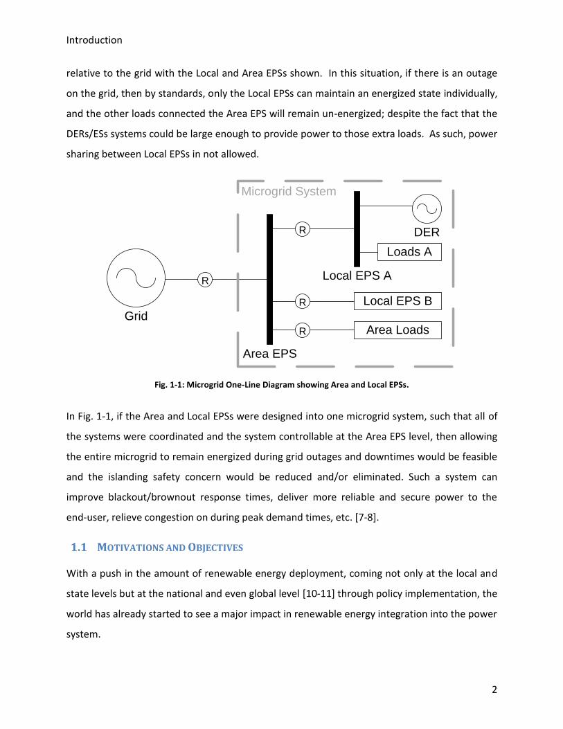
in the system to be larger than necessary. For instance, in Fig. 1-1, a microgrid system is seen
Introduction
2
relative to the grid with the Local and Area EPSs shown. In this situation, if there is an outage
on the grid, then by standards, only the Local EPSs can maintain an energized state individually,
and the other loads connected the Area EPS will remain un-energized; despite the fact that the
DERs/ESs systems could be large enough to provide power to those extra loads. As such, power
sharing between Local EPSs in not allowed.
Grid
R
Area EPS
Local EPS A
R
R
DER
Loads A
R Local EPS B
Microgrid System
Area Loads
Fig. 1-1: Microgrid One-Line Diagram showing Area and Local EPSs.
In Fig. 1-1, if the Area and Local EPSs were designed into one microgrid system, such that all of
the systems were coordinated and the system controllable at the Area EPS level, then allowing
the entire microgrid to remain energized during grid outages and downtimes would be feasible
and the islanding safety concern would be reduced and/or eliminated. Such a system can
improve blackout/brownout response times, deliver more reliable and secure power to the
end-user, relieve congestion on during peak demand times, etc. [7-8].
1.1 MOTIVATIONS AND OBJECTIVES
With a push in the amount of renewable energy deployment, coming not only at the local and
state levels but at the national and even global level [10-11] through policy implementation, the
world has already started to see a major impact in renewable energy integration into the power
system.

Introduction
3
In 2008 alone, the United States added over 10 GW of Wind and Solar generation [8, 10, 12-13].
In conjunction with state/federal mandates and laws requiring not only more “environmentally
friendly” means of energy generation, distribution and use, as well as the increasing trend to
wean the country from fossil fuels, leads to a larger impact renewable energy generation will
have on the grid and its stability. Two key technologies are thus required to enable a high level
of penetration in the grid system: the DERs themselves and ES capacity to store and
supplement the DERs during periods of non-operation (ES is critical for wind and solar
applications where the energy source is intermittent).
A key aspect for quick and widespread implementation of renewable technologies, and to keep
the costs low in such a system, is to create the microgrids at the single-phase (1Φ) distribution
level. This allows for smaller, cheaper DERs/ESs units to penetrate the market quickly and for
the utilities/end-users to install as much capacity as needed to meet local demands within a
microgrid system.
Feasibly, a microgrid system can be comprised of an array of DER and ES units scattered
throughout a system at the Area and Local EPSs levels; potential ES systems that have been
gaining attention are Plug-in Hybrid Electric Vehicles (PHEVs), especially in terms of vehicle
fleets at large facilities, and Community/Residential Energy Storage (CES/RES) systems at
distribution transformers throughout the network.
Grid-coupled PHEV systems allow for Vehicle-to-Grid (V2G) operation that not only gives
charging capabilities to the batteries for transportation needs at residential electricity pricing,
(approximately $0.10/kWh [14] and possibly cheaper if done during non-peak hours) but also
the capability for regenerating the battery’s stored energy for the various ancillary services, as
mentioned above, to allow for PHEVs to be used as controllable loads/sources.
The CES/RES energy storage concepts are currently being developed by consortiums involving
both the American Electric Power (AEP) and Dominion Resources companies. These systems are
primarily aimed at reducing congestion on the transmission and distribution lines at the edge of
the network with secondary objectives to provide power factor correction and emergency
backup power for a limited number of users [7, 15].

Introduction
4
An example of combined PHEV and CES/RES system with miscellaneous DERs implemented at
the 1Φ distribution level can be seen in Fig. 1-2. It is seen that the PHEV and CES/RES can be
charge through the use of DER energy, grid energy, or a combination of the two. Equally so, the
fact that the PHEV and CES/RES can discharge their energy back into the grid and/or provide
STATCOM functionality, or other ancillary services, on demand. The PHEV and/or CES/RES
could also be coordinated to be the voltage/frequency regulator of the microgrid system
depicted during times of grid outages to provide the local loads power as a UPS in conjunction
with the other DERs (outage is transparent to other DERs).
Fig. 1-2: Residential Microgrid System with DER, ES and V2G Applications.
As such, the PHEV and CES/RES systems need to be equipped with bi-directional power
converters (BPCs) and the DERs with VSCs that can operate in the following two modes of
operation:
Grid-Connected Operation
Stand-Alone/Microgrid Operation

Introduction
5
Within each of these modes the following sub-modes can be in operation at any given time
based upon system conditions and/or requests from the facility or an Independent System
Operator (ISO):
AC Current Control
Active/Reactive Power (P/Q) Control
DC Voltage Control
DC Current Control
AC Voltage/Frequency (V/f ) Control
The control systems must be able to operate in all of these modes and be able to change
between them either when commanded to or automatically when a system fault occurs or
protection condition is violated, while minimizing the transient effects of such a change of
mode in operation.
To achieve this, controller design efforts are focused on the following aspects of the control for
1Φ systems:
Microgrid Operation and Control Implementation (Ch 2)
o Linear, Dual Loop Control
Phase-Locked Loops (Ch 3)
o Creation of an improved Phase Detection System
Islanding Detection (Ch 4)
o Through PLL Stability, frequency is forced outside of operational range
Grid Resynchronization (Ch 5)
o Dual PLLs track system to ensure inrush is minimal during reconnection
1.2 LITERATURE OVERVIEW
1.2.1 Benefits of Grid-Connected Renewable Energy Generation and Storage
The electric utility system can benefit from implementing distributed generation technologies,
not only by reducing the amount of electricity generated for new and existing loads, but by
offering the ancillary service capabilities at the distribution level [2, 16].

Introduction
6
Because most generation sites go under-utilized throughout the day (large-scale generation) or
have intermittent fuel sources (PV, wind, etc.), energy storage units have a huge potential to
not only supply peak load demand, but to also perform valley filling in coordination with large-
scale generation sites [8, 16-18].
These same DG technologies can also permit users to capture and reuse thermal energy that
would normally be wasted. Commercial and industrial sites that require large HVAC systems,
such as the data centers and office buildings, as well as metal and chemical processing plants,
refineries, etc., stand to benefit largely from DG implementation for these very reasons [19].
Beyond efficient use of energy, DG technologies may also provide the benefit of more reliable
power for industrial sites in the form of uninterrupted service.
Other than technological benefits, implementation of these ideas can reap other benefits,
including reduced environmental impact, increased economic revenue, and social
understanding of the technologies used in daily lives.
Environmental
Environmentalists and academics have measured and argued that DG technologies provide
benefits to the environment as well, being that large, centralized fossil fuel power plants emit
pollutants (carbon monoxide, dioxins, sulfur oxides, etc.) [11, 19-20]. Moreover, combustion of
fossil fuels tends to create acid rain, which suppresses crop growth and leeches nutrients from
the soil.
Recent studies have begun to confirm that widespread use of DG technologies can substantially
reduce emissions; a British study estimated that domestic CHP production reduced carbon
dioxide emissions by 41% in 1999 (report by the International Energy Agency, [21]). Within the
Danish power system it has been argued that widespread use of DG technologies has reduced
emissions by 30% from 1998 to 2001 [21]. For many years, the U.S. Environmental Protection
Agency (EPA) has also reported the correlation between high levels of sulfur oxide emissions
and significant health effects, including cancer and asthma [22].

Introduction
7
Economic
The Electric Power Research Institute (EPRI) estimates that power outages and quality
disturbances cost American businesses over $100 billion per year [23]. In 2001, the
International Energy Agency estimated that the average cost of a 1-hour power outage was
$6,480,000 for brokerage operations and $2,580,000 for credit card operations [21]. The
figures grow more significantly for the semiconductor industry, where a 2-hour power outage
can cost close to $48,000,000 [23]. Given these numbers, it is clear why several of these critical
industries have already installed DG facilities to ensure uninterruptable power of high levels of
quality.
By building large numbers of localized power generation facilities rather than a few large-scale
power plants located distantly from load centers, DG can contribute to deferring transmission
upgrades and expansions—at a time when investment in such facilities remains constrained
[19, 21, 24].
Social/Policy
Looking locally to within the Commonwealth of Virginia, which experiences in periodic outages,
as well as localized and widespread outages from weather-related events (ice storms and
tropical storms/hurricanes most typically cause these problems), citizen awareness about the
potential of DG technologies and their benefits in situations such as these is extremely low.
Given their general lack of understanding of the utility system, this conclusion comes as little
surprise [20].
As such, trying to grow awareness and enact policies that enable DG technologies to be
implemented within systems is still a major obstacle to overcome. The largest barrier to
widespread DG penetration is the up-front monetary costs. To this end, continuing
technological advances to drive costs down are a must; as well as implementing policy-based
incentives for DG research and installations through distribution networks [16, 19-20, 24].
1.2.2 Converter Architecture and Control Overview
Before any functionality of the system can be implemented, the topology of the converters’
power stage and basic structure of the control system must be established. This may seem like

Introduction
8
an inconsequential step, but it is an important one nonetheless, and one that can affect the
output of the system not only in steady-state, but also during transients and changes between
the modes of operation.
The converter topology, seen in Fig. 1-3, is that of the industry standard, full-bridge voltage
source converter (VSC). This topology was selected due to its versatility in capabilities. The full-
bridge converter can operate with bi-directional power flow, by having the capability to directly
control the output current, which can allow for any of the previously mentioned modes and
sub-modes of operation to be implemented, thus making the converter seem as a controllable
current source to the microgrid, which is useful when paralleling multiple such systems
together.
CDC
L
C VGrid
+
VDC
-
Fig. 1-3: Full-Bridge Topology for VSC.
Control methods such as Droop [25-28], are well suited for parallel converter operation and
regulation of the state variables without communication with a master system or other
converters. However, Droop control tends to produce oscillations during transient response
times and has low bandwidth, which contributes to long settling times to occur before steady-
state is achieved. The other reason Droop control with parallel systems produces oscillations
and long settling times is that energy can resonate between sources until steady-state is
achieved, thus the controllers of each converter are fighting each other to equalize the energy
balance of the system.

Introduction
9
PWM
Voltage Source Converter (VSC)
Control
Law
uDxCy
uBxAx
ˆˆˆ
ˆˆ̂
PWM
Voltage Source Converter (VSC)
Fig. 1-4: Droop Control of VSC. Fig. 1-5: Adaptive Control of VSC.
PWM
Voltage Source Converter (VSC)
PWM
Voltage Source Converter (VSC)
Inner
LoopΣ
Outer
Loop
Fig. 1-6: Sliding Mode Control of VSC. Fig. 1-7: Dual Loop, Linear Control of VSC.
Adaptive- and Predictive-based controllers work extremely well over linear and non-linear
loading conditions, but require the control system to have detailed information of the system at
hand and loads to be modeled in the controller [29-30]. These types of controllers work well in
stand-alone systems where the loading conditions are usually well defined and more or less

Introduction
10
predictable, but in grid-connected systems where the loads can range from linear to non-linear
and with stochastic changes, modeling this type of system is not a small feat to accomplish [29-
34]. Being that the load information needs to be known for these types of controllers, it is near
impossible for a system to accurately and consistently observe what the loading conditions are,
especially when other sources are involved. As such, any benefits gained via this method in
accuracy over a wide loading range is now offset by not only further complexity in the
implementation, but in controller response times as well (controllers can only be as fast as their
load observers that predict the load values for the model).
Sliding mode control is a variable structure control strategy where a surface is selected to which
the control system trajectory experiences a desirable behavior when confined to that surface.
The feedback gain is then determined so that the system trajectory intersects and stays on the
surface [35-38]. In principle, this type of control forcibly constrains the system to stay on the
sliding surface, with the so-called chattering phenomenon being one of the disadvantages of
this control method in that it is possible for the system to limit-cycle as it tries to reach the
desired surface. Another disadvantage of this type of control in a system with multiple modes
of operation is that multiple sliding surfaces are needed for all the modes, and changing the
sliding surfaces depending on the mode of operation is complex and could make it difficult to
maintain stability between such mode transitions. To prevent this, large boundary layers
between the sliding surfaces can be implemented to smooth the transition between surfaces,
but at the cost of control accuracy (the larger the boundary layer to smooth the transition and
the larger the errors produced) [35].
A very simple and effective type of control is the multiple loop, linear PI control system [39-43].
This method uses inner- and outer-linear, PI control loops to regulate the system state
variables. Most commonly, the inner loop provides state feedback control of the AC current
(for grid-connected systems), while the outer loop executes the desired system-level control
function. The inner AC current loop is designed to operate with a bandwidth higher than the
resonant pole frequency of the system filter, while the outer loop is much slower and usually
depends upon the desired control function implemented. This type of control does have

Introduction
11
disadvantages for AC-based systems; the control has finite gain at the fundamental frequency.
As such, zero steady-state error cannot be achieved with PI controllers; PR controllers would
have to be used to eliminate steady-state error at the fundamental frequency if that is a design
requirement [1].
1.2.3 Phase-Locked Loops
A critical aspect for all the modes of operation is the PLL. This component synchronizes the
control system to the grid voltage which takes the AC voltage measurement from the VSC’s
output and generates an estimation of the system frequency, ωest, and phase angle, θest. As
such, θest will track the input angle, θin. Depending on the type of PLL implemented, more
information about the AC voltage can also be discerned from the PLL, such as peak magnitude
and RMS values.
PD LF DCO1
s
sin(θin)
cos(θest)
θestωest
Verr
Fig. 1-8: Basic PLL Functional Structure.
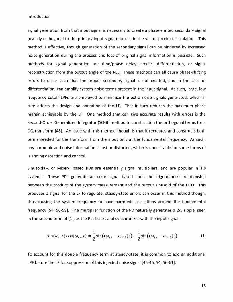
There are three basic elements that a PLL is composed of, seen in Fig. 1-8: the Phase Detector
(PD), the Loop Filter (LF), and the Voltage Controlled Oscillator (VCO). In the case of digital
implementation, this becomes the Digitally Controller Oscillator (DCO) and is a simple
mathematical expression in the controller’s code [44-45].
Phase Detectors (PD)
The most commonly used PD types are: zero-crossing detection (ZCD), vector product, and
sinusoidal multipliers; all of these methods are limited in their response times, accuracy, and/or
application [44-52].
The ZCDs work by sensing the zero crossing of the AC voltage and comparing two crossing
instances to calculate the time (thus frequency) between crossing events. Because of this, ZCD

Introduction
12
PDs suffer from angle estimation inaccuracies and have slow response times to disturbances
due to the inherent half line-cycle delays in the measurements needed for the frequency
calculation [46, 50, 53]. The inaccuracies of this method come from the fact that the system
can only calculate information about ω and θ twice per line-cycle, seen in Fig. 1-9, and cannot
determine system information between these times. The LF in this case, is a simple passive
Low-Pass Filter (LPF). It is needed to reject the jitter effects of multiple zero crossings that can
occur in a real system due to harmonics, switching ripple, sensor noise, etc, and is used to
smooth the discrete jumps in the estimated frequency by averaging. The system transient
response and tracking times are therefore severely increased [46, 53-55], and as such the ZCD
method is rarely used in systems that require detailed information on the sub-cycle level for
control purposes; it is more commonly used as a supplement to other forms of phase detection.
Tline
2
Tline
2
Fig. 1-9: ZCD Time Delay.
ω
Fig. 1-10: Vector Product PD.
Vector product PDs require multiple, independent input variables [44, 50-52], which increases
the system complexity and number of required sensed parameters; vector product PDs are
common in three-phase (3Φ) systems where multiple, independent voltage variables are easily
obtained. This usually comes about in the form of Park’s Transformation, converting the
system from the 3Φ stationary (ABC) to the DQ coordinate frame. In 1Φ systems, vector
product PDs are very complex because there is only one independent voltage variable available;
Introduction
13
signal generation from that input signal is necessary to create a phase-shifted secondary signal
(usually orthogonal to the primary input signal) for use in the vector product calculation. This
method is effective, though generation of the secondary signal can be hindered by increased
noise generation during the process and loss of original signal information is possible. Such
methods for signal generation are time/phase delay circuits, differentiation, or signal
reconstruction from the output angle of the PLL. These methods can all cause phase-shifting
errors to occur such that the proper secondary signal is not created, and in the case of
differentiation, can amplify system noise terms present in the input signal. As such, large, low
frequency cutoff LPFs are employed to minimize the extra noise signals generated, which in
turn affects the design and operation of the LF. That in turn reduces the maximum phase
margin achievable by the LF. One method that can give accurate results with errors is the
Second-Order Generalized Integrator (SOGI) method to construction the orthogonal terms for a
DQ transform [48]. An issue with this method though is that it recreates and constructs both
terms needed for the transform from the input only at the fundamental frequency. As such,
any harmonic and noise information is lost or distorted, which is undesirable for some forms of
islanding detection and control.
Sinusoidal-, or Mixer-, based PDs are essentially signal multipliers, and are popular in 1Φ
systems. These PDs generate an error signal based upon the trigonometric relationship
between the product of the system measurement and the output sinusoid of the DCO. This
produces a signal for the LF to regulate; steady-state errors can occur in this method though,
thus causing the system frequency to have harmonic oscillations around the fundamental
frequency [54, 56-58]. The multiplier function of the PD naturally generates a ripple, seen
in the second term of (1), as the PLL tracks and synchronizes with the input signal.
(1)
To account for this double frequency term at steady-state, it is common to add an additional
LPF before the LF for suppression of this injected noise signal [45-46, 54, 56-61].

Introduction
14
Loop Filters (LF)
The PLL LF can be any form of control function to achieve the desired result of frequency
estimation, and largely depends upon the type of PD used. The LF can be categorized as either
passive or active [62], and can range from simple gains to passive filters to active regulators.
Simple gains, or Proportional control, are the most straightforward to implement, but being
that the PLL is at minimum a 1st-order, Type I control system (due to the integrator following
the LF to generate θest from ωest, modeling of the PLL is seen in Section 3.1), steady-state errors
occur in the frequency estimation. As such, systems that require accurate estimation of ω and
θ steer away from implementing just this type of control.
The same is true for passive filters acting as the LF, though these are LPFs they have less
sensitivity to high frequency noise and harmonics, they suffer from steady-state errors in the
tracking of the input frequency and inject phase delay into the measurement [63-64]. Due to
the passive nature of the LPF, the PLL will become a higher order system, but remain a Type I
control system; therefore, steady-state errors persist and do not force the PD to produce a zero
error voltage which would ensure tracking of the system parameters.
The active LF category itself can be further divided and ranges from linear to non-linear
controllers. Active-based LFs have an important and distinct advantage over passive-based LFs
in that infinite gain at DC through the addition of integrators can be achieved, thus zero steady-
state error in tracking the system frequency is obtained [62-65]. As such, active filters are the
dominant type of LFs used in PLL systems due to the desire to accurately synchronize and track
the input signal. In general, the LF can be made a Type I control system, though depending
upon the complexity of the PD, a Type II controller may be needed to provide zero error to any
disturbance to the system. This will cause the PLL system to become a Type II or higher system.
Of the active types of LFs, the easiest and most common one to implement is a simple PI
regulator. This allows for zero steady-state error, due to the integrator, while the zero allows
for increased system Phase-Margin (PM), thus a reduction in settling time from a transient
disturbance is achieved.
Introduction
15
1.2.4 Islanding Detection
An attractive feature of a microgrid system is that it can operate in a stand-alone mode,
independent of the grid. How to determine when the microgrid should enter such a mode of
operation, and not remain connected to the grid, is an important task for the control to
perform. This is the functionality that islanding detection lends to the control system; sensed
parameters from the system are used to determine when an islanding event has occurred [66-
68]. There are two basic types of detection schemes, passive and active.
Passive Islanding Detection
Passive Islanding Detection schemes passively search for disturbances upon the grid through
sensed and calculated system parameters (voltage, current, frequency, etc.). Such passive
schemes use the tolerance ranges of the voltage (88% - 110% of the nominal voltage) and
frequency (59.3Hz – 60.5Hz) [9] as absolute ratings (for interconnections at the distribution
level), but can also be modified to use additional factors such as rate of change in voltage
and/or frequency [69-70] and change in THD levels [71-72] as well.
The main issue with passive detection schemes is that they can produce Non-Detection Zones
(NDZs) [73-75]. These NDZs are conditions that the DERs/ESs units are operating at, but when a
fault or islanding condition occurs, the system continues to run under acceptable operating
conditions. This is most commonly the case when a DER/ES is operating at near load-matching
conditions; in which the current delivered to/from the grid is virtually zero. In such a case, if a
relay upstream from a DER/ES in a Local EPS trips, and the grid is disconnected, the control will
not see this event because the grid was not supplying the load with any power. Because the
load demand was being generated by the DER/ES, the system will continue to track itself and
operate as normal, as seen in (2) – (7), and assuming that the DER/ES units are relatively close
to the loads in a Local EPS system (DER/ES units and loads are not weakly coupled).
To illustrate how NDZs can affect the system, it will be assumed that a DER/ES unit and the grid
feed a parallel RLC load and will solve for the islanded voltage and frequency. The DER/ES
active power output, PDG, can be expressed in terms of the grid voltage (V) and an effective
resistance (Reff) or expressed in terms of the islanded voltage (Visland) and actual load resistance

Introduction
16
(R); along with load power demand, this is seen in (2). The effective resistance that the DER
sees while grid connected is stated in (3). Combining (2) and (3), the islanded voltage can be
calculated in (4). From this, it is easy to see that if the DER/ES’s active power output closely
matches the load demand, the islanded voltage will remain close to the nominal grid voltage.
(2)
(3)
(4)
In terms of the how the islanded frequency will behave, assuming the same parallel RLC load,
the following is seen. The reactive power load impedance is seen in (5) and can be calculated
either by the load’s islanded frequency value or by the DER/ES power delivered to the load. By
equating these two ways of finding this impedance, a quadratic function can be found, seen in
(6), which describes the islanded frequency. Defining a load quality factor, Qf seen in (6), and
solving for the islanded frequency, the result in (7) [73, 76] is obtained.
(5)
(6)
(7)
From (4) it is clear to see that if PDG ≈ Pload, then the islanded voltage stays at the nominal
value, and any mismatch will cause deviation from the nominal (ie: PDG > Pload Visland > V, and

Introduction
17
vice versa). From (7), assuming the worst case of DER/ES load matching for its output power,
then it can be easily derived that if the reactive load’s resonant frequency is matched to the
nominal frequency, then the islanded frequency will be driven to resonant value. Otherwise,
mismatches in the active power and reactive power and the load resonant frequency will
contribute to deviations in the islanded frequency compared to the nominal system frequency.
In general though, it can be summarized that the reactive power mismatch parameter has an
inverse effect upon islanded frequency compared to the nominal value
(ie: QDG > Qload ωisland < ω, and vice versa).
+ΔP
Over-Voltage
-ΔP
Under-Voltage
+ΔQ
Under-Frequency
-ΔQ
Over-Frequency
NDZ
ΔP(pu)
ΔQ(pu)
0
0 Fig. 1-13: NDZ area for DG Power Mismatches.
The effects from (4) and (7) can be seen in Fig. 1-11 and Fig. 1-12, respectively, while Fig. 1-13
summarizes the NDZ for power mismatches for a given Qf. The NDZ will shrink and grow in this
Fig. 1-11: Voltage Deviation for
Active Power Mismatch. Fig. 1-12: Frequency Deviation for Reactive Power
Mismatch (assuming Active Power load match).

Introduction
18
figure with respect to Qf, and assuming active load mismatch is approximately zero. From this,
it is clear to see that detection methods that rely on passive schemes will always be subject to
NDZs; therefore, under close load matching conditions an islanding event can be missed
entirely.
Active Islanding Detection
Active detection schemes (while incorporating aspects of the passive schemes, [71]) are usually
embedded within the system level control loops of converter system. Active schemes are
better at sensing islanding disturbances and reducing/eliminating the NDZs that the passive
ones cannot, but at the cost of system performance [72].
Common types of active detection inject harmonics into the output of the system to sense for
islanding events and depending upon how much of a perturbation and power mismatch there
is, these schemes will drive the voltage and/or frequency away from the nominal values and out
of the NDZs; however, this usually degrades the power quality of the output to the system
(perturbations usually inject harmonics or distort the power factor angle into the system, thus
increasing the THD delivered to the grid [68, 72, 77]).
Other common types of active detection involve perturbations of the Active and Reactive
Power/Current and/or Voltage level [66, 76, 78-82]. These methods have the drawback that
they continuously perturb the system, and though these perturbations can be absorbed with
only a handful of sources in a relatively strong grid producing such effects, when system
penetration is high and/or the grid system is weak, then these perturbations could cause
system-wide instabilities in the voltage and frequency [68, 71-72, 74].
A different type of active method involves frequency perturbations, such as the Active
Frequency Drift (AFD) method; it uses injected variances in frequency to distort the current
reference of an inner AC current control loop [83-87]. The issue with these methods is that
they rely on the distortion of the current to force the system voltage and frequency to drift
when an islanding event occurs, and depending upon the amount of frequency drift
implemented the current distortion can be fairly large, as seen in Fig. 1-14. As such, this causes

Introduction
19
the grid to produce a pulsed power feature to compensate for the distorted current being
generated by the DER/ES system(s).
Fig. 1-14: AFD Current Distortion for 1Φ Systems.
The Active Phase-Shifting (APS) method utilizes a low frequency (typically less than 1/10th the
line frequency) oscillation to perturb the power factor angle [88-90]. Thus, it is equivalent to
actively perturbing the reactive power of the system; in this case the perturbation is done over
such a long time period (10’s of cycles) that the effect is absorbed as a load transient upon the
system. This method, however, has the same issues as the others in that if multiple systems are
implemented, even the low frequency perturbation can distort and destabilize the grid; NDZs
are also still possible in APS methods.
Two common types of APS methods that are often implemented in systems are derivatives of
the Sandia Frequency Scheme (SFS) and the GE Frequency Scheme (GEFS) [83, 87]. In these
methods, system transients are converted into control perturbations to affect the power factor
angle, seen in Fig. 1-15 and Fig. 1-16. The advantages of these schemes is that they reduce the
amount and times of the perturbations injected into the system, and depend upon a positive
feedback mechanism, (8), to drive the loads outside the NDZs to where over/under voltage and
frequency protection (OVP/UVP, OFP/UFP) schemes can sense the islanding event.

Introduction
20
ωest ΔIq QDG ωisl
(8)
One issue with the SFS is that it uses a ZCD PLL. This can be updated to a faster, more accurate
PLL, but the system is still limited in detection speed by the washout functions necessary to
generate the phase-shift term.
The GEFS has the issue of requiring a 1Φ, DQ PLL. As mentioned before, 1Φ vector product PDs
in the PLL can be troublesome in the generation of the secondary, phase-shifted signal, causing
artificial noise to appear in the measurements and distort the output of the system.
Fig. 1-15: SFS Islanding Detection.
Fig. 1-16: GEFS Islanding Detection.

Introduction
21
1.2.5 Grid Resynchronization
The ability to reconnect to the grid from an islanded mode of operation is critical for the
operation of a DER/ES-based system. In a microgrid, the DER/ES systems are generally not
designed to run in the Stand-Alone/Microgrid mode of operation for extended periods of time;
this is especially true for systems that have little to no ES capacity. As such, it is desired that
when the grid clears a fault, or other islanding condition(s), which caused the microgrid to enter
the stand-alone mode, that it reconnect to the grid as quickly as possible [6, 68, 91-93] while
maintaining all standard requirements of IEEE 1547-2003 [9].
There are two basic parameters that the islanded system must meet to be able to reconnect to
the grid: 1) the voltage magnitude of islanded systems cannot be more than ±5% of the grid
voltage magnitude, and 2) the phase difference between grid and islanded voltages must meet
the requirements of Table 5 in [9] (< 20° for systems < 500 kVA). Failure to meet and/or exceed
these requirements can generate large inrush currents to/from the grid that are orders of
magnitude above system limits [91, 93]. This can damage not only the DER/ES systems, but the
grid transmission equipment and attached loads as well.
Because it is critical to minimize the phase difference between the two systems before
reclosure, fast and accurate estimations of the phase angles of these two systems is
paramount; hence requiring a good PLL system.
Common types of reclosure algorithms to the grid are open loop in nature. Once the system
has identified that the grid has been reestablished (a fault was cleared or temporary outage
over), the control marginally increases the islanded system’s frequency. When phase alignment
has occurred, checked through simple logical routines, the microgrid is reclosed to the grid and
the control changes back to grid connected mode of operation [92].
Microgrid Setup and Control Operation
22
2. Microgrid Setup and Control Operation
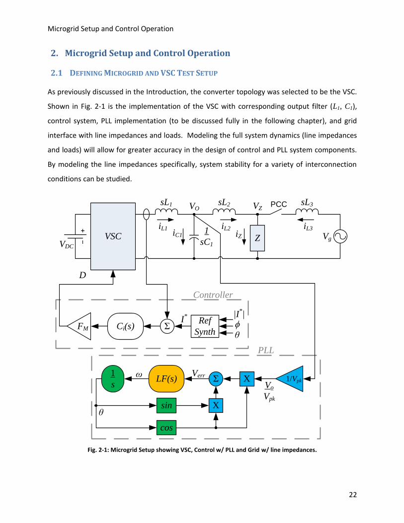
2.1 DEFINING MICROGRID AND VSC TEST SETUP
As previously discussed in the Introduction, the converter topology was selected to be the VSC.
Shown in Fig. 2-1 is the implementation of the VSC with corresponding output filter (L1, C1),
control system, PLL implementation (to be discussed fully in the following chapter), and grid
interface with line impedances and loads. Modeling the full system dynamics (line impedances
and loads) will allow for greater accuracy in the design of control and PLL system components.
By modeling the line impedances specifically, system stability for a variety of interconnection
conditions can be studied.
VSC
sL1 sL3sL2
Z1
sC1
Vg
iL1 iL2 iL3iC1 iZ
VO VZ
FM Ci(s) Σ
|I*|I*
Σ XVo
Vpk
cos
sin X
LF(s)1
s
θ
ω
Controller
PLL
Verr
D
Ref
Synthf
VDC
θ
1/Vpk
PCC
Fig. 2-1: Microgrid Setup showing VSC, Control w/ PLL and Grid w/ line impedances.

Microgrid Setup and Control Operation
23
The output filter of the VSC is designed to filter harmonics < 11th (fundamental = 60 Hz). To
start, the converter’s base impedance is found, seen in Table I with other system parameter
values. The filter inductance, L1, impedance is selected to be between 5-10% of the VSC’s rated
impedance. This is done to ensure that there is not excessive voltage drop across the filter and
to ensure good coupling to the AC bus of the grid system. The output capacitor, C1, is then
selected such that the cutoff frequency of the filter is between the 10th and 11th line harmonic.
TABLE I: SYSTEM PARAMETERS
Parameter Value (unit)
Vpk (V)
VDC 265 (V)
ωline 2π∙60 (rad/s)
fsw, Tsample 20k (Hz), 50μ (s)
Srated 2k (VA)
7.2Ω
L1, L2, L3 1.2m, 10μ, 10μ (H)
C1 50μ (F)
Zsimulated
R = 25Ω
// RLC = 25Ω, 66.3mH, 106μF
// RLC = 25Ω, 45.5mH, 150μF
// RLC = 25Ω, 26.5mH, 265μF
Zexperimental R = 25Ω
// RLC = 25Ω, 45.5mH, 150μF
1.0, 1.4, and 2.5 (simulated)
1.4 (experimental)
for Z = // RLC case
FM 1
ψ 0 (rads)
The other line impedances, L2 and L3, are included in the model to simulate transmission and
distribution line reactances. These were selected to be a fraction of the output filter value to
ensure that a strong and dominant grid system is maintained. In later analysis, the effects of
increasing these values, essentially making the grid a weaker system, are discussed.

Microgrid Setup and Control Operation
24
Along with the aforementioned components of the microgrid, is the grid point of common
coupling (PCC) relay. This relay is governed by the islanding detection (Chapter 4) and
Resynchronization (Chapter 5) algorithms to be discussed. Its purpose is to isolate the
microgrid in the event of grid loss or other islanding events, and to reconnect to the grid once
reestablished and synchronize.
The remainder of Table I states the VSC electrical properties, such as nominal AC and DC bus
voltages, switching and sampling times, and loads used in simulations and experiments (unless
otherwise denoted).
(Generalized system setup of Fig. 2-1 is assumed for all simulated and experimental results
unless otherwise noted; detailed setup of simulation circuits via MatLab Simulink are found in
Appendix A, details and the setup of the hardware and digital control systems are found in
Appendix B, and DSP code for experimental results is in Appendix C.)
2.2 SYSTEM MODES OF OPERATION
As mentioned before, there are two general modes of operation that a microgrid must account
for and operate in:
Grid-Connected Mode (GCM)
Stand-Alone/Microgrid Operation (SAM)
Within these two modes are several sub-modes of operation that the system must be able to
regulate in:
AC Current Control
Active/Reactive Power (P/Q) Control
DC Voltage Control
DC Current Control
AC Voltage and Frequency (V&f) Control
o (only to be used in Stand-Alone/Microgrid Operation when system is
disconnected from the main grid)

Microgrid Setup and Control Operation
25
2.2.1 Grid-Connected Mode
From Fig. 2-2, it is seen that there are three states of control operation the system could be in
as a grid-connected converter. The central state is the Grid-tied AC Current mode, and
regulates the AC current being sourced to/from the grid. This can take the form of multiple
applications such as current or power regulation. The other two states are the Grid-tied
Rectifier and the Grid-tied Charger/Discharger modes.
The Rectifier mode is such that the DC voltage is regulated and is useful for DER/ES systems
that have multiple source/load combinations on the DC link. The Charger/Discharger mode is
used primarily for battery and other ES systems. In this mode, either the DC link current or
power is regulated to perform the desired charging/discharging effects.
Grid-tied
AC Current
Mode
Grid-tied
Rectifier
Mode
Grid-tied
Charger/
Discharger
Mode
Stand-alone
Mode
1. Detect loss of grid and disconnect
2. Use last good phase/frequency reading from
PLL to set initial conditions for voltage mode
outer loop
3. Enable outer voltage loop
4. Disable PLL tracking, used as oscillator for
voltage mode.
1. Sense DC-link variable and set as
the initial reference value
2. Enable outer loop controller
3. Ramp reference to the desire value
1. Sense DC-link Voltage, VDC
2. Lookup table w/ charge/discharge current levels
3. Enable outer loop controller
4. Ramp reference to desired values within limitations.
1. Read I*AC output of outer
loop, and set as the initial
reference value
2. Disable outer loop
controller
3. Ramp reference to the
desired value
1. Grid is back, enable PLLtracking
2. PLL detects phase and tracks, voltage mode output
is synchronized with grid voltage
3. Keep in voltage mode until relay is closed
4. Once relay closed, disable voltage mode controller,
initialize current mode.
Fig. 2-2: State Machine Flowchart of when/how Mode Transitions occur.

Microgrid Setup and Control Operation
26
2.2.2 Microgrid/Stand-Alone Mode
From Fig. 2-2, it is seen that there is only one state of operation that the system can run in for
the Stand-Alone mode. This mode, once the system is disconnected from the grid, regulates
the AC voltage and frequency of the Local and Area EPS(s). Other DER/ES systems within the
microgrid can then track the new system voltage and frequency and act as if they were in a
GCM. This setup is assuming the system is in a master/slave configuration where one control
system regulates system V&f and all others follow (future work described in Section 6.2 would
deal with parallel source coordination for control the AC bus during SAM).
If the system demands more power than what the DER/ES can supply, then the control system
enters a current limit mode to protect itself (of which is present for any of the modes of
operation if the power source/sink demand is too large).
In such a situation, there are three options the control system can choose from: 1) transfer V&f
regulation to another system in the microgrid and go into current source mode (this is
essentially going back to a grid-connected mode of operation), 2) reduce non-critical load
demand (load shaving) to allow system to come back into equilibrium, or 3) shutdown
completely.
The third choice is not a desired situation and should only be considered for events that cause
potential damage to the system. As such, the first option is the most attractive, while the
second is still not as desirable, it can be necessary to maintain functionality to critical loads
within EPS(s).
2.2.3 Transitioning between Modes of Operation
In Fig. 2-2, all mode changes are routed through the current mode of operation. This allows all
transitions to be tightly controlled and minimizes transient surges, or dropouts, while changing
the outer loop functionality.
Since the inner AC current loop is always active, when a mode change is requested, the control
freezes the last AC current reference, and uses that as the new initial reference point during the
transition and for the new mode of operation.
Microgrid Setup and Control Operation
27
The following example outlines this concept. When changing from the SAM to any of the
GCMs, the following is performed (these steps assumed the necessary synchronization steps and
relay reclosure have already taken place):
1. Mode Change Requested;
2. Control Calculates last good current reference value in SAM and freezes it;
3. System is now operating in a constant current mode while new control configurations
are implemented;
4. New mode control activated, and frozen reference value set as initial condition for new
mode;
5. Constant current control released, and new mode fully active.
2.3 VSC CONTROL IMPLEMENTATION AND OPERATION
Of the controller options previously discussed, the multi-loop, linear PI system is selected and
implemented, as seen in Fig. 2-3 and Fig. 2-4, due in large to its simplicity, versatility in control
capabilities, and robustness against instabilities between changes in the modes of operation.
Seen in Fig. 2-3, the inner loop is selected to regulate the AC current of the system, while the
outer loop can be any controller form which generates a current reference to achieve the
desired function of the sub-mode of operation. Whereas the outer loop generates an AC
current reference for the inner loop to track, the inner loop generates the system duty-cycle
that is sent to the converter’s modulator and gate-drive system.
Fig. 2-4 details how the inner and outer loops of the control system operate together. As
mentioned, a fundamental principle of this method is that no matter which mode of operation
the system is in, the inner AC current loop is always active, as seen in Fig. 2-5. This is done not
only for system protection, the AC current is regulated with a limiting value such that over-
current situations cannot occur due to the control system, but it is implemented this way to
help increase stability and reduce transient effects during the changes between the modes of
operation.

Microgrid Setup and Control Operation
28
CDC
L
C VGrid
+
VDC
-
AC Current
Loop ΣPWMOuter
ControlRef
Fig. 2-3: Multi-loop Control System for a VSC.
AC Current
Loop Σ
Duty-Cycle
X
iAC
i*AC
sin(θ+f)
|i*AC|
Outer Loop
Reference
Generation
Fig. 2-4: AC Current Reference Generation for GCM outer loops.
PLL
P/Q
LPF
Σ
Modulator
+
+-
-1
Hidc
HVdc
V/f
AC Current
Loop
iAC VAC
Σ
To VSC
GCM
SAM
Fig. 2-5: Multi-loop control showing AC Current Loop always active w/ various outer loop configurations.

Microgrid Setup and Control Operation
29
Because the inner loop is always active, when a change in the mode of operation occurs, this
transient event in the functionality will now look like a step/ramp response to the inner loop
and the rest of the converter system [68, 77].
Previous methods found in literature change the control depending upon the mode by changing
the entire control structure (both the inner and outer loops entirely) [6, 92-93]. These methods
work, but minimizing the transient effects between the mode changes and having multiple
control systems track one another to keep stability issues from arising is a challenging task to
implement.
2.3.1 Stationary Frame Control
Selecting a particular coordinate reference frame of the control system can both help and
hinder the transient and steady-state responses of a system. In this study’s control
implementation, the stationary reference frame is used.
In the stationary frame, the controlled state-variables are time-varying, sinusoidal signals. As
such, with PI regulators implemented for the inner and outer loops, steady-state errors can
occur. These errors however, are relatively insignificant to have large impacts on the system,
especially since the inner AC current loop bandwidth is pushed beyond the resonant pole of the
converter’s output filter (which will depend ultimately on the filter design, but should be
roughly 10x the line-frequency). Also in this reference frame, no signal adjustments are
required on the sensed variables, other than LPFs to attenuate the switching frequency and
higher order harmonics, which allows for simple implementation of the control system in the
digital realm.
2.3.2 Inner AC Current Loop Design Features
As mentioned, the only restrictions placed upon the inner AC current loop is that it must have a
bandwidth larger than the resonant pole of the converter’s output filter (AC side LC filter), and
the outer loops’ control bandwidth must be significantly lower than the resonant pole’s
frequency location. This causes the inner loop to look transparent to the outer loop in terms of
the effects it has on the system, and allows for good noise rejection due to load perturbations

Microgrid Setup and Control Operation
30
(bandwidth crossover frequency is well above the resonant pole, as such, the system can
regulate load ranges from no-load to full-load without complications).
Fig. 2-6: Open Loop TFs for inner AC current loop control design.
The open loop transfer functions seen in Fig. 2-6 show various control-to-AC current conditions;
including: SAM inverter operation, GCM inverter operation, GCM rectifier operation, etc. (full
derivation of transfer functions can be found in [94]). Seen is how the resonant pole of the
system changes for various modes of operation and loading conditions; however it is noticed
that the SAM inverter application yields highest pole frequency. As such, if the inner AC current
loop is designed meet this mode of operations worst-cases, then the controller will work for all
other modes of operation as well.
It should be noted that since the controller is designed for the SAM, when the converter is in
the GCM, this control system will not be optimized, and performance will be slightly degraded
from what it could be. This is an acceptable tradeoff to incur such that the control system can
be streamlined, and ensure interoperability between the modes of operation. Hence, a simple
-100
-50
0
50
100
150M
ag
nit
ud
e (
dB
)
102
104
106
108
-135
-90
-45
0
45
90
Ph
ase (
deg
)
Bode Diagram
Frequency (Hz)
stand_inverter
grid_inverter
grid_rectifier 5 Ohms
grid_rectifier 50 Ohms
grid_rectifier 150 Ohms

Microgrid Setup and Control Operation
31
linear, PID control system can be used to generate a closed-loop AC current loop with high
bandwidth with suitable Nyquist criterion.
2.4 CONTROL OPERATION WITHIN THE DIFFERENT MODES
In essence, all of the modes of operation for any situation are AC current regulated; the outer
loop control system generates the AC current references to drive the system to fulfill the
specified objectives of the outer loop.
The following sections describe and present examples of some of the sub-modes of operation
within the GCM and SAM.
2.4.1 Bidirectional Charger/Discharger/Rectifier
In the charger/discharger and rectifier modes of operation described in Fig. 2-2, power flow can
be bidirectional, assuming the DC link of the converter system has some form of ES capability
and/or DC loading. Depending on which functionality is desired, the DC voltage, DC current, or
power flow value will be used in the outer loop controller to generate an AC current reference;
either from an active regulator or through a mathematical function, which in turn will drive the
system to fulfill the desired functionality of the outer loop.
In the DC voltage case, a PI controller regulates the system to the desired DC voltage. In the DC
current case, regulation can be achieved via two methods: a simple PI regulator can directly
control the system (assuming DC current is a sensed variable to control), or the desired value
can be used to generate the required DC power to be delivered/exported, which in turn is used
similarly to the P/Q control scheme (seen in the following section) to generate the AC current
reference; either of these methods will give accurate results.
The simulation setup can be found in Appendix A, and was implemented in MatLab’s Simulink
simulation program. The converter and system modeling techniques used, assumptions made,
controller values, and Simulink implementation are all described in detail there. All other values
are assumed to be those of Table I.

Microgrid Setup and Control Operation
32
Shown in Fig. 2-7 – Fig. 2-12 are the simulated results for the Charger/Discharger mode. The DC
current reference is ramped from zero to 5A (discharging), then to -5A (charging). The DC
current in Fig. 2-7 looks like a full-wave, rectified sinusoid, because no inductor was added to
filter this ripple. The AC side waveforms, of current and voltage, are seen in Fig. 2-8 through
Fig. 2-12 and show how the current being sourced/sinked to/from the grid behaves for DC
current control. Shown is a reflection of the DC link current direction in the phase-reversal of
the AC current generated and magnitude transition between sourcing and sinking energy from
the grid. The zoomed in waveforms show the transitions in detail and at the point in which the
system changes sourcing/sinking energy to/from the grid interconnect.
The hardware and experimental setup can be found in Appendix B. There, the sensing and
control board implementation is overviewed and described, as well as specific converter details.
Unless otherwise denoted in the following sections or in the appendix itself, system parameters
are assumed to be that in Table I.
Hardware results in Fig. 2-13 and Fig. 2-14 are for the charging and discharging of a PHEV
battery into the grid. Seen is how the when the DC current is ramped from positive to negative
(and vice versus), that the AC current follows suit with its phase reversal and magnitude scaling,
as was seen in the simulations of Fig. 2-8. In these figures it should also be noticed that current
waveforms produced are very sinusoidal in nature and contain low levels of noise and
harmonics.
In all the performance of the experimental results correlates very well with the expected
outcomes predicted by the simulations.
In the hardware results it is seen that the DC current does not have the same ripple as in the
simulations. A large inductor was connected between the VSC and the battery system to filter
the ripple, which protects the battery from large oscillating currents (which can create thermal
cycling issues).
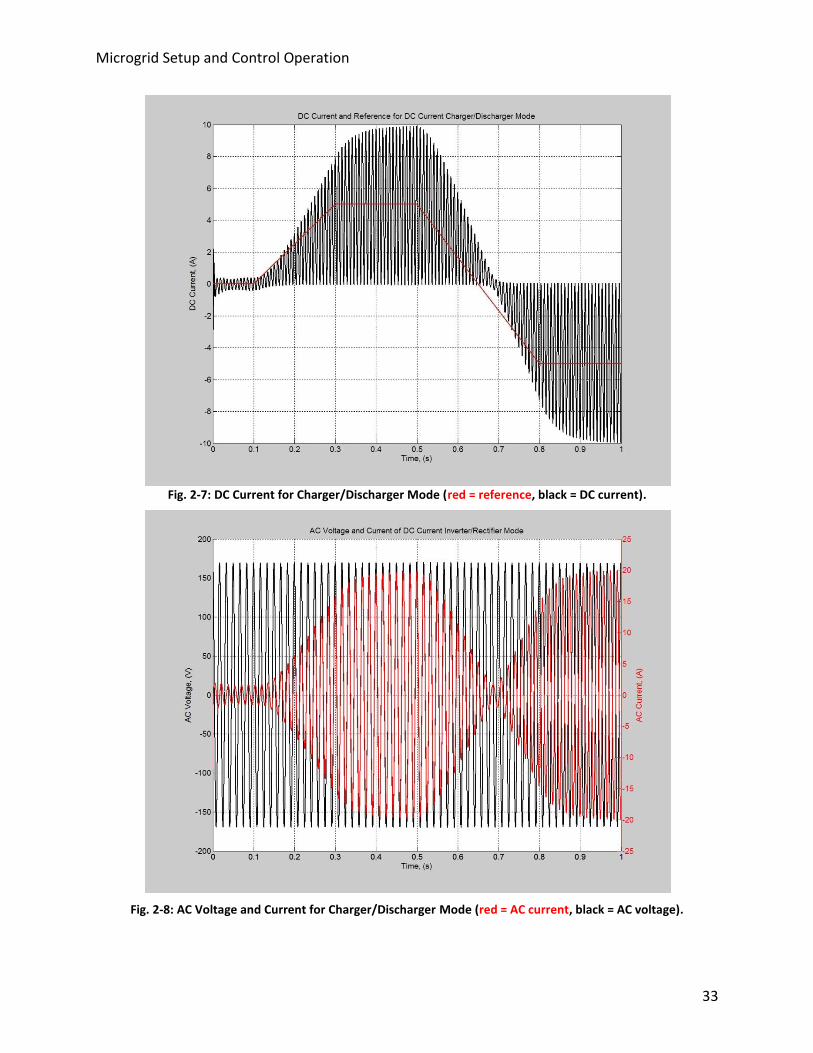
Microgrid Setup and Control Operation
33
Fig. 2-7: DC Current for Charger/Discharger Mode (red = reference, black = DC current).
Fig. 2-8: AC Voltage and Current for Charger/Discharger Mode (red = AC current, black = AC voltage).

Microgrid Setup and Control Operation
34
Fig. 2-9: AC Voltage and Current for Charger/Discharger Mode zoomed in during positive DC Current ramp up
(red = AC current, black = AC voltage).
Fig. 2-10: AC Voltage and Current for Charger/Discharger Mode zoomed in during positive DC Current ramp
down (red = AC current, black = AC voltage).

Microgrid Setup and Control Operation
35
Fig. 2-11: AC Voltage and Current for Charger/Discharger Mode zoomed in during DC Current sign inversion
(red = AC current, black = AC voltage).
Fig. 2-12: AC Voltage and Current for Charger/Discharger Mode zoomed in during negative DC Current ramp up
(red = AC current, black = AC voltage).
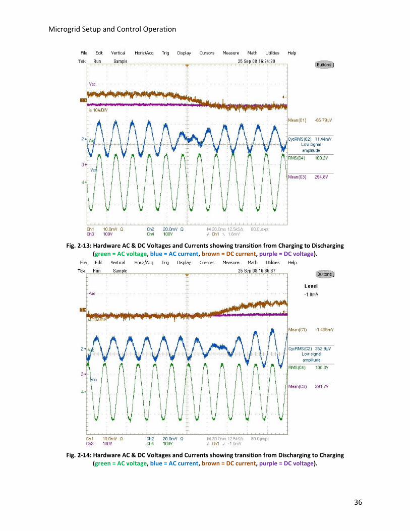
Microgrid Setup and Control Operation
36
Fig. 2-13: Hardware AC & DC Voltages and Currents showing transition from Charging to Discharging
(green = AC voltage, blue = AC current, brown = DC current, purple = DC voltage).
Fig. 2-14: Hardware AC & DC Voltages and Currents showing transition from Discharging to Charging
(green = AC voltage, blue = AC current, brown = DC current, purple = DC voltage).
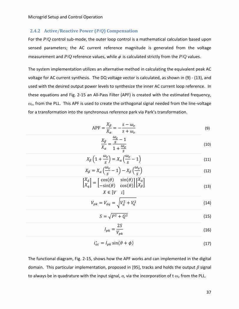
Microgrid Setup and Control Operation
37
2.4.2 Active/Reactive Power (P/Q) Compensation
For the P/Q control sub-mode, the outer loop control is a mathematical calculation based upon
sensed parameters; the AC current reference magnitude is generated from the voltage
measurement and P/Q reference values, while is calculated strictly from the P/Q values.
The system implementation utilizes an alternative method in calculating the equivalent peak AC
voltage for AC current synthesis. The DQ voltage vector is calculated, as shown in (9) - (13), and
used with the desired output power levels to synthesize the inner AC current loop reference. In
these equations and Fig. 2-15 an All-Pass Filter (APF) is created with the estimated frequency,
ωe, from the PLL. This APF is used to create the orthogonal signal needed from the line-voltage
for a transformation into the synchronous reference park via Park’s transformation.
(9)
(10)
(11)
(12)
(13)
(14)
(15)
(16)
(17)
The functional diagram, Fig. 2-15, shows how the APF works and can implemented in the digital
domain. This particular implementation, proposed in [95], tracks and holds the output β signal
to always be in quadrature with the input signal, α, via the incorporation of t ωe from the PLL.

Microgrid Setup and Control Operation
38
Fig. 2-15: APF/Orthogonal Generation Block Diagram.
The input and output of the APF is used in (13) to create the DQ voltage vector seen in (14).
This result is then passed through a LPF to extract the DC component, thus eliminating
harmonic and noise content (only interested in the fundamental component features). The
resultant value is the peak amplitude of said fundamental component of the input voltage.
As such, this value is used with the apparent power reference, S, to generate the peak AC
current magnitude reference; while the active/reactive references are used to solve for the
power factor angle. The PLL supplies the base voltage angle, and a current sinusoid is
synthesized to be used in the regulation by the inner current loop, seen in (14) – (17). The
simulation and hardware setups can be found in Appendix A and Appendix B.
The following simulations, Fig. 2-16 – Fig. 2-20, show the P/Q control for various steps in
reactive power (corresponding to shifts between unity and 60°); observed are how smooth
transitions from one reference value to the next is obtained through the inner AC current loop
(no extraneous current spikes or fluctuations observed).
Hardware results seen in Fig. 2-21 show a step from 60° lagging PF to unity during a
regenerative mode of operation. Noticed in this capture is how the sudden jump in PF angle (as
in the simulated cases) does not cause current surges to be produced while the converter is
adjusting its output to track the new reference. Though not implemented, this jump in PF angle
can be smoothed out via ramp-rate limiters in the PF inclusion of the AC current synthesis.
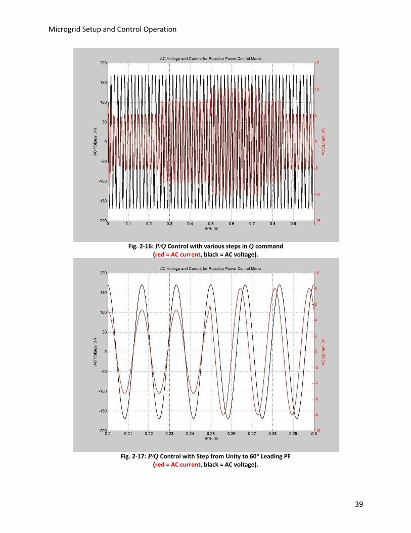
Microgrid Setup and Control Operation
39
Fig. 2-16: P/Q Control with various steps in Q command
(red = AC current, black = AC voltage).
Fig. 2-17: P/Q Control with Step from Unity to 60° Leading PF
(red = AC current, black = AC voltage).
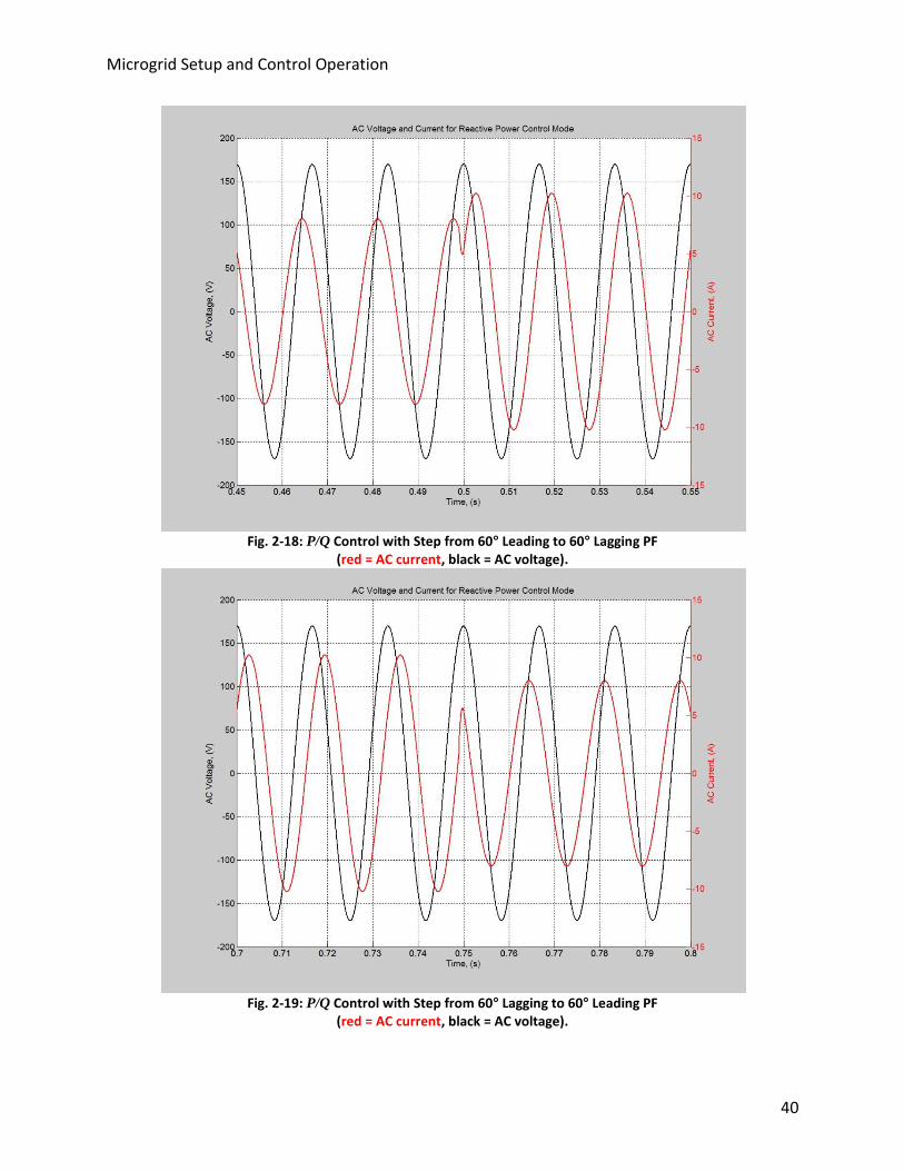
Microgrid Setup and Control Operation
40
Fig. 2-18: P/Q Control with Step from 60° Leading to 60° Lagging PF
(red = AC current, black = AC voltage).
Fig. 2-19: P/Q Control with Step from 60° Lagging to 60° Leading PF
(red = AC current, black = AC voltage).

Microgrid Setup and Control Operation
41
Fig. 2-20: P/Q Control with Step from 60° Leading to Unity PF
(red = AC current, black = AC voltage).
Fig. 2-21: Hardware P/Q Control with Step from 60° Leading to Unity PF while Discharging a PHEV Battery
(green = AC voltage, blue = AC current, brown = DC current, purple = DC voltage).

Microgrid Setup and Control Operation
42
2.4.3 Voltage/Frequency Regulation
This sub-mode is reserved strictly for the Stand-Alone/Microgrid mode. In this mode, the
converter regulates the AC V&f of the Local and Area EPSs. Depending upon the microgrid
conditions, the converter (assumed to have some sourcing and/or ES capabilities) can regulate
power flow to/from of the DC link to provide stable, accurate and clean AC voltage waveforms
for the EPS(s).
In this mode of operation, the outer loop changes, as with the other sub-modes of operation, to
regulate the voltage and frequency on the AC bus. A simple PI regulator with bandwidth just
above the line-frequency was used. The simulation and hardware setups can be found in
Appendix A and Appendix B.
In Fig. 2-22 and Fig. 2-23, respectively, waveforms showing the minute steady-state error
(practically negligible due to the high bandwidth of the inner AC current loop controller) and
the AC voltage and current during load transients. Seen in Fig. 2-23 are load steps of full to half
to regenerative to half to full; Fig. 2-24 – Fig. 2-27 show the zoomed in transitions in detail.
These waveforms demonstrate that in SAM, the system can source/sink energy as needed
(sinking of energy will depend upon the ES capabilities and conditions) while maintaining a high
quality level of the AC voltage. Particularly notable, is how the controller can regulate power
flow bidirectionally to maintain the proper AC voltage waveform. This again is an effect of
having an inner AC current tailored for all modes of operation and with high closed-loop
bandwidth.
Hardware results in Fig. 2-28 show V&f regulation for a combined resistive, non-linear loading,
while Fig. 2-29 shows regulation for just the non-linear loading. Seen in each is how under
commonplace and extreme loading conditions, the outer and inner loops can regulate the
system to produce good and stable voltage and frequency references for the loads.

Microgrid Setup and Control Operation
43
Fig. 2-22: AC Voltage and Reference for Stand-Alone Mode
(red = AC current, black = AC voltage).
Fig. 2-23: AC Voltage and Current from VSC during Load Steps in Stand-Alone Mode
(red = AC current, black = AC voltage).

Microgrid Setup and Control Operation
44
Fig. 2-24: AC Voltage and Current from VSC during Full- to Half-Load
(red = AC current, black = AC voltage).
Fig. 2-25: AC Voltage and Current from VSC during Half- to Regenerative-Load
(red = AC current, black = AC voltage).

Microgrid Setup and Control Operation
45
Fig. 2-26: AC Voltage and Current from VSC during Regenerative- to Half-Load
(red = AC current, black = AC voltage).
Fig. 2-27: AC Voltage and Current from VSC during Half- to Full-Load
(red = AC current, black = AC voltage).

Microgrid Setup and Control Operation
46
Fig. 2-28: Hardware Results showing V&f control for a Resistive and Non-linear Load
(green = AC voltage, blue = AC current, brown = DC current, purple = DC voltage).
Fig. 2-29: Hardware Results showing V&f control for just the Non-linear Load
(green = AC voltage, blue = AC current, brown = DC current, purple = DC voltage).

Single-Phase, Phase-Locked Loops
47
3. Single-Phase, Phase-Locked Loops
One of the critical elements required for precise control of power converters that are grid-
connected is the Phase-Locked Loop (PLL). In these systems, the PLL is responsible for tracking
and synchronizing with the frequency and phase angle of the grid voltage. Otherwise,
inaccurate, and potentially harmful, control of power factor, harmonics, and the determination
of the system mode of operation can result [44, 48, 55, 58, 91, 96-97].
3.1 PHASE-LOCKED LOOP MODELING
In order to design a proper PLL system, it must first be modeled. Fig. 3-1 shows the method in
which the Open Loop (OL) Transfer Function (TF), from frequency to error voltage, is derived for
a PLL with the Standard Mixer Phase Detector (SMPD). This TF is key to the design of the PLL
Loop Filter (LF).
Assuming ideal conditions, and that the perturbation propagates uniformly through θe and the
PLL oscillator (DCO) (which is not an unreasonable assumption [62-65]), it is seen in (18) and
(19) that the PLL is nothing more than a integrator with gain equal to the cosine of the phase
angle mismatch, ψ, between the grid and the PLL. Fig. 3-2 shows the MatLab Simulink Bode
response of such a system, showing good agreement with the calculated value.
Fig. 3-1: OL Calculation from frequency to Voltage error for Standard Mixer PD (SMPD).
(18)
(19)

Single-Phase, Phase-Locked Loops
48
Fig. 3-2: OL Transfer Function of PLL from Simulink.
3.1.1 Loop Filter Design
With an OL model in place, the PLL system LF can be designed. With numerous types of
controllers that could be considered for the LF, this work simply uses a PI regulator, unless
otherwise stated, to create a baseline for comparison in noise reduction performance seen in
the subsequent sections, and for reasons further explained in Chapter 4.
In [98], the authors showed how when full system dynamics, like those found in Fig. 2-1, are
included in the calculations, the OL response of the PLL is simply an integrator with a gain, again
confirming (19) for the SMPD case.
With the approximation of the system solved for via the modeling above, a basic mathematical
model of the PLL can be used to calculate how the LF affects steady-state and transient
performance, and is seen in Fig. 3-3.

Single-Phase, Phase-Locked Loops
49
LF1
s
θeVerr ωeΣ
-
+θi θerrK
G(s)
Fig. 3-3: Basic Mathematical Model of PLL for System Approximations.
In (20), the forward path of the plant/control system can be grouped together as G(s). As
mentioned, the LF is a PI regulator and takes the form in (21). The PD gain, K, is kept generic
throughout the derivation as KPD to reflect various effects that the PD implementation can
have on the modeling.
(20)
(21)
(22)
(23)
(24)
Solving the CL, output equation, Hout(s), the system can be described by (22). Converting to the
standard, 2nd order, natural frequency format of (23), the performance factors are found as
functions of the LF and PD gains. Comparing (22) and (23), these factors are solved for in (24).
The classical response trade-off, of optimizing settling-time and overshoot, is seen in Fig. 3-4,
and was obtained via the following LF design guidelines.
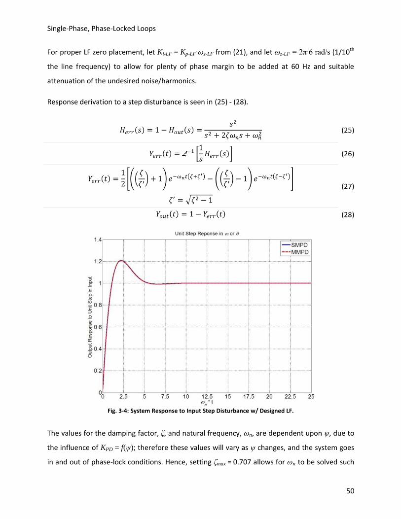
Single-Phase, Phase-Locked Loops
50
For proper LF zero placement, let Ki-LF = Kp-LF∙ωz-LF from (21), and let ωz-LF = 2π∙6 rad/s (1/10th
the line frequency) to allow for plenty of phase margin to be added at 60 Hz and suitable
attenuation of the undesired noise/harmonics.
Response derivation to a step disturbance is seen in (25) - (28).
(25)
(26)
(27)
(28)
Fig. 3-4: System Response to Input Step Disturbance w/ Designed LF.
The values for the damping factor, ζ, and natural frequency, ωn, are dependent upon ψ, due to
the influence of KPD = f(ψ); therefore these values will vary as ψ changes, and the system goes
in and out of phase-lock conditions. Hence, setting ζmax = 0.707 allows for ωn to be solved such

Single-Phase, Phase-Locked Loops
51
that settling-time and overshoot trade-off are now optimally minimized, while avoiding the
over-damped system response [62]. Other gains can be selected to vary the trade-off between
settling-time and overshoot as required by individual specifications; this study uses the above
conditions in comparison between implementations and operating conditions.
Fig. 3-5 and Fig. 3-6 show the Loop Gain (LG) and CL Nyquist plots, respectively, and that the
system has reasonable stability margins and meets the Nyquist Criteria for the controller gains
shown in (29).
(29)
Fig. 3-5: Loop Gain TF with LF implemented (created w/ (19) and (29) in MatLab’s SISOTool Box).
10-1
100
101
102
-180
-150
-120
-90P.M.: 41.3 deg
Freq: 5.27 Hz
Frequency (Hz)
Phase (
deg)
-30
-20
-10
0
10
20
30
40
50
60
70
G.M.: -Inf dB
Freq: 0 Hz
Stable loop
Open-Loop Bode Editor for Open Loop 1 (OL1)
Magnitu
de (
dB
)
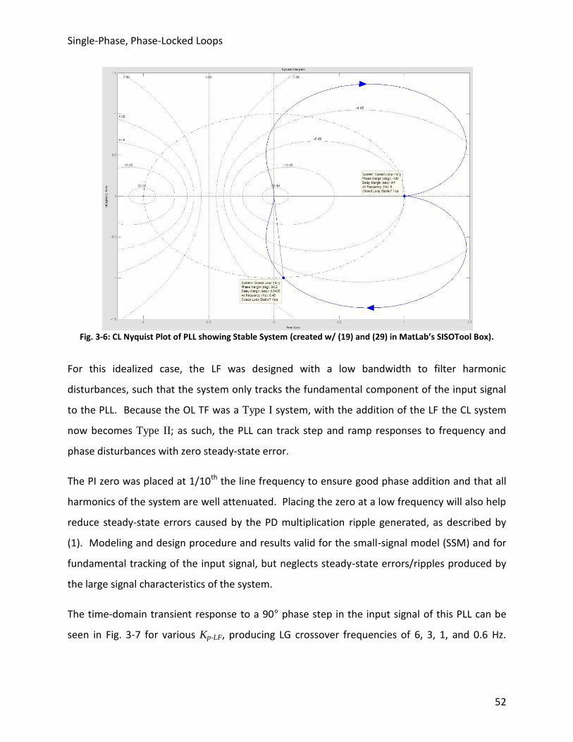
Single-Phase, Phase-Locked Loops
52
Fig. 3-6: CL Nyquist Plot of PLL showing Stable System (created w/ (19) and (29) in MatLab’s SISOTool Box).
For this idealized case, the LF was designed with a low bandwidth to filter harmonic
disturbances, such that the system only tracks the fundamental component of the input signal
to the PLL. Because the OL TF was a Type I system, with the addition of the LF the CL system
now becomes Type II; as such, the PLL can track step and ramp responses to frequency and
phase disturbances with zero steady-state error.
The PI zero was placed at 1/10th the line frequency to ensure good phase addition and that all
harmonics of the system are well attenuated. Placing the zero at a low frequency will also help
reduce steady-state errors caused by the PD multiplication ripple generated, as described by
(1). Modeling and design procedure and results valid for the small-signal model (SSM) and for
fundamental tracking of the input signal, but neglects steady-state errors/ripples produced by
the large signal characteristics of the system.
The time-domain transient response to a 90° phase step in the input signal of this PLL can be
seen in Fig. 3-7 for various Kp-LF, producing LG crossover frequencies of 6, 3, 1, and 0.6 Hz.
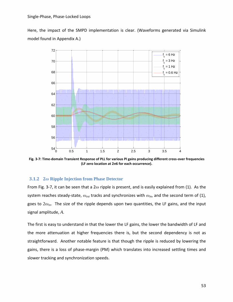
Single-Phase, Phase-Locked Loops
53
Here, the impact of the SMPD implementation is clear. (Waveforms generated via Simulink
model found in Appendix A.)
Fig. 3-7: Time-domain Transient Response of PLL for various PI gains producing different cross-over frequencies (LF zero location at 2π6 for each occurrence).
3.1.2 2ω Ripple Injection from Phase Detector
From Fig. 3-7, it can be seen that a 2ω ripple is present, and is easily explained from (1). As the
system reaches steady-state, ωest tracks and synchronizes with ωin, and the second term of (1),
goes to 2ωin. The size of the ripple depends upon two quantities, the LF gains, and the input
signal amplitude, A.
The first is easy to understand in that the lower the LF gains, the lower the bandwidth of LF and
the more attenuation at higher frequencies there is, but the second dependency is not as
straightforward. Another notable feature is that though the ripple is reduced by lowering the
gains, there is a loss of phase-margin (PM) which translates into increased settling times and
slower tracking and synchronization speeds.
0 0.5 1 1.5 2 2.5 3 3.5 454
56
58
60
62
64
66
68
70
72
fc = 6 Hz
fc = 3 Hz
fc = 1 Hz
fc = 0.6 Hz

Single-Phase, Phase-Locked Loops
54
For the SMPD, the input signal should ideally be at unity amplitude, therefore producing the
trigonometric identity in (1). However, to achieve this, the AC voltage must be divided by the
peak value, which in real systems is constantly changing about a nominal value. As such, A
(which is also known as the per unit value of the voltage) can be included in the equations and
quantified. For completeness, the equations shown are for when the grid and PLL are not
synchronized, and a phase difference/mismatch term, ψ, is present, as seen in (30).
(30)
Through this expansion and reduction, it is seen that a DC term, due to ψ, is now present. As
the PLL synchronizes with the grid, this DC term goes to zero, and Verr is again left with a 2ω
ripple term; though now the effect of A has on the ripple is clear.
Fig. 3-8: Effects of added LPFs to reduce 2ω ripple in PLL.
As previously discussed in Chapter 1, a standard way to reduce this undesirable ripple term is to
add large LPFs before the LF to attenuate this ripple. This method became the standard way,
not because it worked the best, but because it was simplest to implement and with reasonable
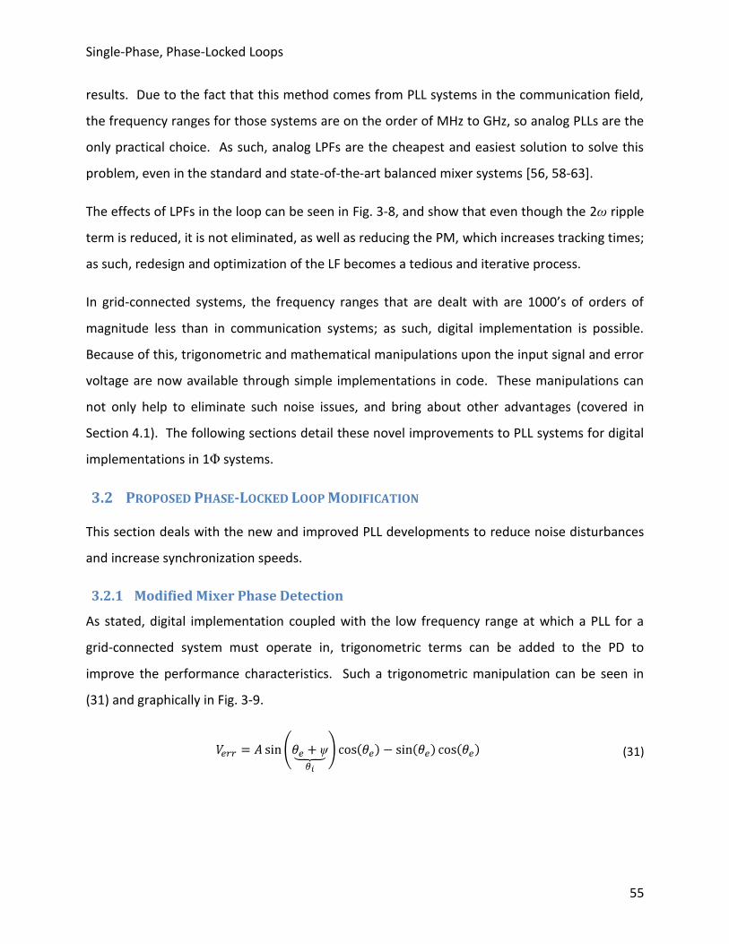
Single-Phase, Phase-Locked Loops
55
results. Due to the fact that this method comes from PLL systems in the communication field,
the frequency ranges for those systems are on the order of MHz to GHz, so analog PLLs are the
only practical choice. As such, analog LPFs are the cheapest and easiest solution to solve this
problem, even in the standard and state-of-the-art balanced mixer systems [56, 58-63].
The effects of LPFs in the loop can be seen in Fig. 3-8, and show that even though the 2ω ripple
term is reduced, it is not eliminated, as well as reducing the PM, which increases tracking times;
as such, redesign and optimization of the LF becomes a tedious and iterative process.
In grid-connected systems, the frequency ranges that are dealt with are 1000’s of orders of
magnitude less than in communication systems; as such, digital implementation is possible.
Because of this, trigonometric and mathematical manipulations upon the input signal and error
voltage are now available through simple implementations in code. These manipulations can
not only help to eliminate such noise issues, and bring about other advantages (covered in
Section 4.1). The following sections detail these novel improvements to PLL systems for digital
implementations in 1Φ systems.
3.2 PROPOSED PHASE-LOCKED LOOP MODIFICATION
This section deals with the new and improved PLL developments to reduce noise disturbances
and increase synchronization speeds.
3.2.1 Modified Mixer Phase Detection
As stated, digital implementation coupled with the low frequency range at which a PLL for a
grid-connected system must operate in, trigonometric terms can be added to the PD to
improve the performance characteristics. Such a trigonometric manipulation can be seen in
(31) and graphically in Fig. 3-9.
(31)

Single-Phase, Phase-Locked Loops
56
X LFA sin(θi) 1
s
θeVerr ωe
Σ
X
cos
sin
-
+
Fig. 3-9: Modified PD for improvement in PLL performance.
As before, expanding the term Verr and determining how A and ψ affect the PLL performance,
(32) - (37) are found (for shorthand, let θ = θe = ωet).
(32)
(33)
(34)
(35)
(36)
(37)
From (36) it is seen how A and ψ affect Verr, but if (36) is taken a step further, and it is assumed
that A ≈ 1 then (37) can be derived. From (37), it can be easily seen that as ψ goes to zero, so
does Verr. This Modified Mixer PD (MMPD) is an improvement over the LPF method, which
would require an impractical LPF, with a cutoff frequency at zero, to achieve these same results
in steady-state. Furthermore, the design of the LF for the MMPD is exactly the same as in the
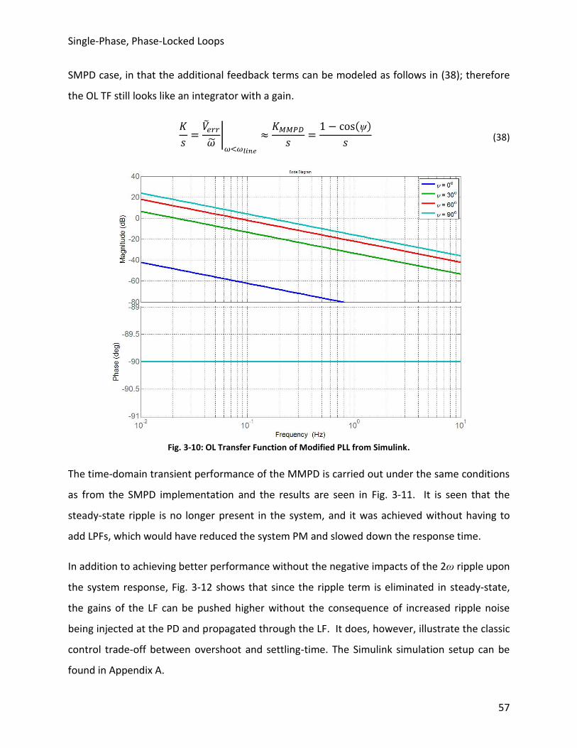
Single-Phase, Phase-Locked Loops
57
SMPD case, in that the additional feedback terms can be modeled as follows in (38); therefore
the OL TF still looks like an integrator with a gain.
(38)
Fig. 3-10: OL Transfer Function of Modified PLL from Simulink.
The time-domain transient performance of the MMPD is carried out under the same conditions
as from the SMPD implementation and the results are seen in Fig. 3-11. It is seen that the
steady-state ripple is no longer present in the system, and it was achieved without having to
add LPFs, which would have reduced the system PM and slowed down the response time.
In addition to achieving better performance without the negative impacts of the 2ω ripple upon
the system response, Fig. 3-12 shows that since the ripple term is eliminated in steady-state,
the gains of the LF can be pushed higher without the consequence of increased ripple noise
being injected at the PD and propagated through the LF. It does, however, illustrate the classic
control trade-off between overshoot and settling-time. The Simulink simulation setup can be
found in Appendix A.

Single-Phase, Phase-Locked Loops
58
Fig. 3-11: Time-domain Transient Response of Modified PLL.
Fig. 3-12: Time-domain Transient Response of Modified PLL.
0 0.5 1 1.5 2 2.5 3 3.5 457
58
59
60
61
62
63
64
65
66
67
fc = 6 Hz
fc = 3 Hz
fc = 1 Hz
fc = 0.6 Hz
0 0.5 1 1.5 2 2.5 3 3.5 450
55
60
65
70
75
fc = 30 Hz
fc = 15 Hz
fc = 12 Hz
fc = 6 Hz
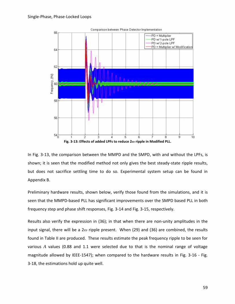
Single-Phase, Phase-Locked Loops
59
Fig. 3-13: Effects of added LPFs to reduce 2ω ripple in Modified PLL.
In Fig. 3-13, the comparison between the MMPD and the SMPD, with and without the LPFs, is
shown; it is seen that the modified method not only gives the best steady-state ripple results,
but does not sacrifice settling time to do so. Experimental system setup can be found in
Appendix B.
Preliminary hardware results, shown below, verify those found from the simulations, and it is
seen that the MMPD-based PLL has significant improvements over the SMPD based PLL in both
frequency step and phase shift responses, Fig. 3-14 and Fig. 3-15, respectively.
Results also verify the expression in (36); in that when there are non-unity amplitudes in the
input signal, there will be a 2ω ripple present. When (29) and (36) are combined, the results
found in Table II are produced. These results estimate the peak frequency ripple to be seen for
various A values (0.88 and 1.1 were selected due to that is the nominal range of voltage
magnitude allowed by IEEE-1547); when compared to the hardware results in Fig. 3-16 - Fig.
3-18, the estimations hold up quite well.

Single-Phase, Phase-Locked Loops
60
The results seen in Fig. 3-19 show the PLL performance of both PD implementations under
extremely distorted line conditions. Even under this very ill condition, the MMPD out performs
the SMPD and generates over a 50% reduction in the ripple compared to the SMPD.
TABLE II: ESTIMATED FREQUENCY RIPPLE DUE TO INPUT AMPLITUDE GAIN
PD Implementation A (p.u.) Δf (Hz, peak) % Δf reduction
SMPD A = 0.88
1.05 85.7%
MMPD 0.15
SMPD A = 1.0
1.19 100%
MMPD 0
SMPD A = 1.1
1.31 90.8%
MMPD 0.12
Fig. 3-14: MMPD (blue) and SMPD (brown) PLL responses to a 2Hz step in the AC Voltage.

Single-Phase, Phase-Locked Loops
61
Fig. 3-15: MMPD (blue) and SMPD (brown) PLL responses to a 90° shift in the AC Voltage.
Fig. 3-16: MMPD (blue) and SMPD (brown) PLL responses under nominal AC Voltage.
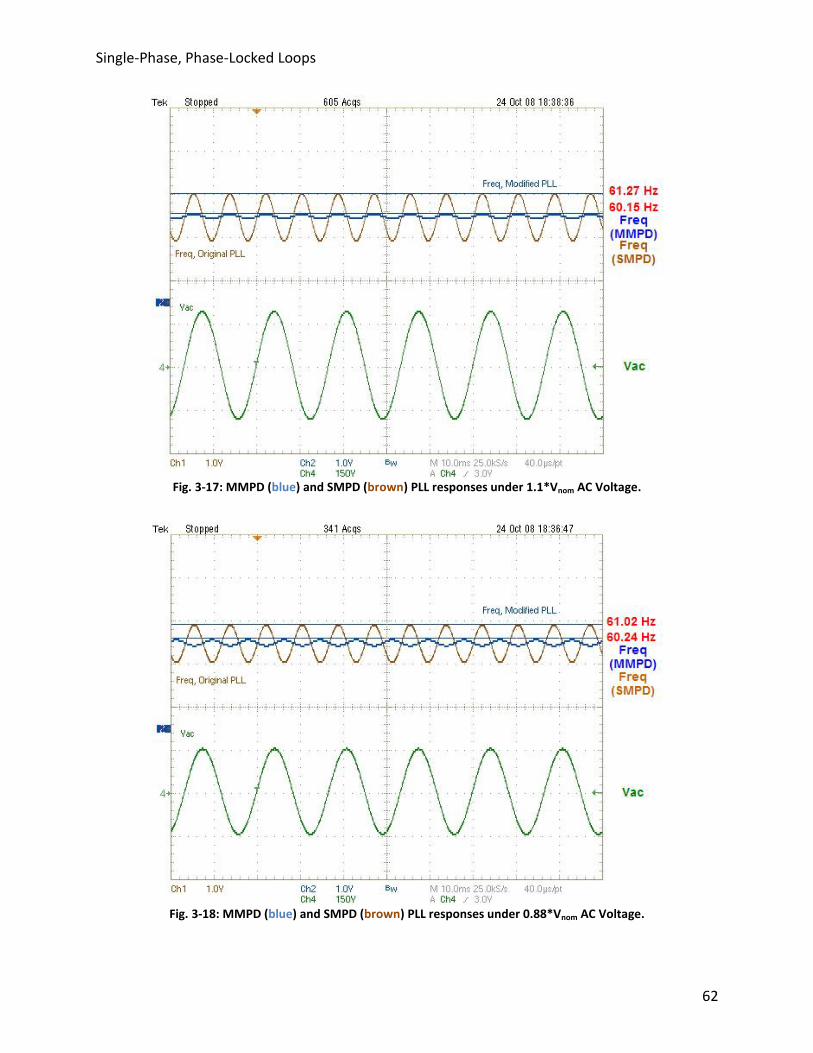
Single-Phase, Phase-Locked Loops
62
Fig. 3-17: MMPD (blue) and SMPD (brown) PLL responses under 1.1*Vnom AC Voltage.
Fig. 3-18: MMPD (blue) and SMPD (brown) PLL responses under 0.88*Vnom AC Voltage.

Single-Phase, Phase-Locked Loops
63
Fig. 3-19: MMPD (blue) and SMPD (brown) PLL responses under Distorted AC Voltage (green) (22.9% THDV).
3.2.2 Non-linear, Adaptive Frequency Feedback
The implementation of the MMPD showed how injected ripple noise can be reduced through
the feedback of θe. To improve the synchronization speed/settling-time of transients in the
input, a Frequency Feedback (FFB) term can be added to the LF, as seen in Fig. 3-20.
X LFA∙sin(θi) 1
s
θeVerr Δωe
Σ
X
cos
sin
X
KFFB
-
+Σ
ωe
ωff
Fig. 3-20: MMPD-based PLL with Dynamic Gain Adjustment via FFB.

Single-Phase, Phase-Locked Loops
64
When the added feedback term of the error frequency, Δωe, is multiplied with Verr the system
changes form and creates a non-linear, adaptive-like control system [99]. The FFB term is seen
in (39), where the sgn(ωe) ensures that the FFB term is positive and K'FFB is a user defined gain;
while (40) and (41) show how the FFB impacts the normally linear LF gains and the
corresponding performance characteristics.
(39)
(40)
(41)
In (40), the effect of the FFB term on the LF gains shows that due to the selection of ωz-LF, (21),
only the overall control gain changes, the location of ωz-LF remains fixed. Therefore, the FFB
term dynamically adjusts the overall LF gain depending upon the frequency error generated by
the LF. This gain change leads to the possibility that the LF encounters ζmax > 1 and ωn-max > ωn
as ψ changes; which is not necessarily a drawback.
Plainly stated, with this implementation, as ψ → 90°, ωn becomes larger, as does ζ; thus the
system will resist the move to 90° out of phase-lock and forces the PLL back into
synchronization with the input signal. However, smaller values of ψ leads to ζ << 1, and an
under-damped system will be created; resulting in larger overshoots but with faster
synchronization speeds. As such, when the system is not in phase-lock, i.e. ψ ≠ 0, the FFB gain
will scale Verr, resulting in an increase in synchronization speed, but at the cost of overshoot
(classical control problem of determining K'FFB trade-off of settling-time vs. overshoot).
The only drawback to this implementation is that it requires an A ≈ 1 to operate properly.
When A ≠ 1, any noise ripple created by the PD will be amplified via this gain, and the
estimated frequency will incur an increase in noise ripple due to this method. This is simply
solved by adding a peak voltage tracker prior to the input of the PLL to ensure that the input
amplitude is always A ≈ 1; as such, the method used to generate (14) can be used to ensure

Single-Phase, Phase-Locked Loops
65
unity gain at the input of the PLL PD. The simulated and experimental test setups are found in
Appendix A and Appendix B.
In Fig. 3-21, the simulated results showing the effect that the MMPD w/ FFB term has on the
transient response compared against the normal MMPD case. With FFB, the settling-time is
reduced by ~57%; but as seen, at the cost of a much higher overshoot (PLL saturates as
Δf = 15 Hz limits).
When a non-unity gain input to the PLL is present, i.e. A 1, the FFB term is seen to amplify the
ripple well beyond the original SMPD ripple (shown is A = 1.05 for MMPD w/ FFB), Fig. 3-22. As
mentioned, adding peak voltage tracking of the PLL input to ensure that A ≈ 1 at all times can
easily be implemented. This approach was implemented, with the results observed in Fig. 3-23.
It is seen that when the input magnitude is tracked, such that A ≈ 1, the MMPD with the FFB
term applied shows significant improvements in settling-time. From the results, reduction is
~55%, which is in good accordance with the simulated results.
Fig. 3-21: MMPD w/ and w/o FFB and A = 1.

Single-Phase, Phase-Locked Loops
66
Fig. 3-22: Limitations of MMPD w/ FFB when A ≠ 1.
Fig. 3-23: MMPD w/ and w/o FFB and Peak Detection Input Tracking.

Single-Phase Islanding Detection
67
4. Single-Phase Islanding Detection
Islanding detection schemes are useful to avoid energizing an Area EPS during fault conditions
and grid disconnections (as required by Standard IEEE-1547). Islanding conditions not only lead
to unsafe and unreliable power delivery between the sources and loads, but can potentially
cause damage to equipment as well as raising safety concerns for workers and users.
In addition to detecting faults on the grid, islanding detection algorithms play another key role
in microgrid systems: through the detection of grid abnormalities, these methods allow the
control system to decide on an appropriate operational mode.
Ideally, islanding detection algorithms inherently sense abnormalities and disconnections of the
grid, while functioning normally during all other operating modes and without injecting
distortions into the grid to test for these conditions. Namely, passive detection methods, [72,
76, 100], perform this functionality, but are susceptible to NDZs, as previously noted in
Chapter 1.
In the stationary frame, the most common islanding detection methods for 1Φ operation are
the AFD and APS methods. As discussed in Chapter 1, these methods require continuous
perturbations and/or distort the converter’s output; as such, these types of islanding detection
methods can lead to power quality issues as well as stability concerns. Therefore, it is desired
to have an islanding detection method that does not continuously perturb the system to
potentially cause such issues, but instead only perturbs and tests for islanding conditions for
the events themselves.
Through the design and use of the MMPD PLL (from Chapter 3) and a VSC, a detection scheme
can be crafted. Essentially, through the use of the conditionally stable PLL, the loss of grid
islanding event is the trigger for detection perturbations. To ensure proper operation of the
PLL and detection system when coupled with the entire system, the MMPD-based PLL is
modeled with its full system interactions and dynamics accounted for, which include control,
grid and line/load parameters.
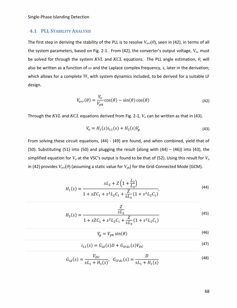
Single-Phase Islanding Detection
68
4.1 PLL STABILITY ANALYSIS
The first step in deriving the stability of the PLL is to resolve Verr(θ), seen in (42), in terms of all
the system parameters, based on Fig. 2-1. From (42), the converter’s output voltage, Vo, must
be solved for through the system KVL and KCL equations. The PLL angle estimation, θ, will
also be written as a function of ω and the Laplace complex frequency, s, later in the derivation;
which allows for a complete TF, with system dynamics included, to be derived for a suitable LF
design.
(42)
Through the KVL and KCL equations derived from Fig. 2-1, Vo can be written as that in (43).
(43)
From solving these circuit equations, (44) - (49) are found, and when combined, yield that of
(50). Substituting (51) into (50) and plugging the result (along with (44) – (46)) into (43), the
simplified equation for Vo at the VSC’s output is found to be that of (52). Using this result for Vo
in (42) provides Verr(θ) (assuming a static value for Vpk) for the Grid-Connected Mode (GCM).
(44)
(45)
(46)
(47)
(48)
Single-Phase Islanding Detection
69
(49)
(50)
(51)
(52)
The reference current magnitude, |I*|, and load power factor angle, , are supplied from higher
level controller(s), or are static for constant current controllers. For this derivation each are
assumed to be as such to supply the full load demand of Z; therefore the grid current, iL3, is
ideally zero; which will give the worst case detection condition (i.e. maximizing the NDZ
created).
The small-signal model linearization of (42) with (52) leads to the desired transfer function to
use with the previous design methodology of the LF and check for system stability. Linearizing
about θ allows for its extraction from the trigonometric functions in Verr, as seen in (53).
(53)
(54)
(55)
(56)
As such, this leads to (54). To find Verr(ω), θ is simply converted to ω via (55), which yields the
result in (56). With this transfer function defined and solved for, LF design and PLL stability can
now be checked.

Single-Phase Islanding Detection
70
Note: The derivations performed are for the MMPD cases; the SMPD derivations are not shown,
but the end results are identical to (56) with the change in that the “-1” term is no longer
present within the bracket.
Graphically seen in the Bode plots of Fig. 4-1 and Fig. 4-2 for various values of ψ, both the
MMPD and SMPD implementations generate high frequency components. For the frequency
range ω < ωline, the previous modeling efforts of a decoupled PLL remain valid. As seen, the real
changes come at higher frequencies, which do not affect PLL LF design and performance (for
moderate to relatively strong grid dominance), but can start to affect VSC controller design. As
such, the highest inner AC current loop bandwidth should be limited by these higher frequency
resonant effects. The MatLab M-file code used to generate these TFs and plots can be found in
Appendix A.
Fig. 4-1: Verr / ω for various ψ of MMPD in GCM.
Single-Phase Islanding Detection
71
Fig. 4-2: Verr / ω for various ψ of SMPD in GCM.
For the Grid-Disconnect Mode (GDM), the same derivation is performed, and H1(s) and H2(s) of
(44) and (45) are re-derived as (57) and (58). The final format still remains that of (56).
(57)
(58)
For the GCM and GDM, Bode plots of (56) are seen in Fig. 4-3 (MMPD) and Fig. 4-4 (SMPD). The
system parameters used are from Table I. When (56) is expanded for the MMPD GCM and GDM
cases, a 7th order polynomial with integrator results, (59) and (60).

Single-Phase Islanding Detection
72
Fig. 4-3: Verr / ω for MMPD w/ Z = R & RLC (Qf = 2.5) for GCM and GDM.
Fig. 4-4: Verr / ω for SMPD w/ Z = R & RLC (Qf = 2.5) for GCM and GDM.

Single-Phase Islanding Detection
73
(59)
(60)
The coefficients for the polynomial in (60) are found in (61) – (74).
(61)
(62)
(63)
(64)
(65)
(66)
(67)
(68)
(69)
(70)

Single-Phase Islanding Detection
74
(71)
(72)
(73)
(74)
From this analytical expansion, there are several cancellations between the numerator and
denominator, which is plainly seen when the parameters of Table I are evaluated and the
numeric pole/zero combinations are observed.
When ψ is included in the expansion, as a summation with θ (as seen in the coefficient values),
the results yield the high frequency poles/zeroes as seen in Fig. 4-3 and Fig. 4-4. Looking at the
2nd order terms of the numerator and denominator, (66) and (72), of the expansion are
analyzed, the resonant frequencies of the pole/zero combinations in (75) and (76) are found.
These resonances, seen in Fig. 4-1 – Fig. 4-4, appear at higher frequencies (>10 kHz for the
given parameters in Table I), and are due to the L1C1 filter (L1 ≈ 5% Zrated which attenuates
harmonics > 10th of ωline), line impedances L2 and L3 (each ~1% of L1) and load interactions.
(75)
(76)

Single-Phase Islanding Detection
75
Seen in (76) is a floating zero dependent upon ψ. It is noticed that as the PLL synchronizes, this
zero moves to the origin, while when the PLL approaches 90° of phase mismatch, the zero
approaches the resonant pole in (75). In the SMPD, this floating zero does not exist. It should
be pointed out that these locations are for resistive loads. The locations of the resonances will
have dependencies on the load; as such, the above equations for these values will change
slightly, but not significantly. Therefore, it will be assumed that the equations describe the
pole/zero placement despite loading conditions.
In Fig. 4-3 for the MMPD GDM, the TF reverts to what is essentially a negative integrator (with
resonances at higher frequencies due to (75) and (76)). This trait of the MMPD in GDM is used
to produce a simple, yet effective, Islanding Detection Scheme covered in following sections.
As seen from Chapter 3 and previously, the GCM for SMPD and MMPD will be stable for a
simple, PI LF design. Also of note from Fig. 4-3 was that in the GDM, the MMPD case presented
creates inherently unstable OL conditions. Hence, for any MMPD GDM case, the maximum PM
that can be achieved is -90° for PI LF types.
Therefore, with the OL system always unstable in the GDM, and the frequency will oscillate and
drift away from the nominal value in CL; final drift speed and location is still dependent upon
loading conditions, and can be calculated using (7). Through this mechanism, a standard
over/under frequency protection (OFP/UFP) scheme can then be used to help detect islanding
events.
Conversely, for the SMPD’s GDM, the system may remain stable and with little change in
frequency; Fig. 4-2 shows this stable OL case for GDM. Hence the GDM with a PI LF can
essentially track itself and not become unstable, oscillate, and drift away from the nominal
frequency range. This leads to the creation of larger NDZs which can leave an Area EPS
energized when a grid disconnect or other islanding fault occurs upstream.
Using the Z = R case as a simple example, the Nyquist plots in Fig. 4-5 and Fig. 4-6 are observed,
which shows GDM for MMPD and SMPD respectively; explicitly shown is how the MMPD case
becomes unstable while the SMPD case does not.

Single-Phase Islanding Detection
76
The MMPD creates a system that contains a clockwise encirclement of the -1 point in the
Nyquist plot; while the SMPD shows to have a counter-clockwise path that does not encircle
the -1 point. Because of this, the MMPD case violates the Nyquist criterion for stable operation
while SMPD meets it.
This stability check through the Nyquist criterion shows the conditional stability of the MMPD-
based PLL system between the GCM and GDM, and allows for a simple, yet effective, islanding
detection method to be created in conjunction with an OFP/UFP scheme.
Fig. 4-5: MMPD Nyquist showing Encirclement of -1.

Single-Phase Islanding Detection
77
Fig. 4-6: SMPD Nyquist showing no Encirclement of -1.
4.2 QUASI-ACTIVE ISLANDING DETECTION USING PLL STABILITY
With nothing more than simple OFP/UFP as the islanding detection mechanism, the stability of
the MMPD PLL will force the system outside the nominal operational range, seen in Fig. 4-7,
and trip the system into a different mode of operation. Thusly, a quasi-active islanding
detection scheme has been created. The system is only perturbed when the frequency goes
unstable and begins to oscillate, but this only happens under grid disconnect conditions. Note:
only the MMPD is presented in simulated and hardware results, of which Appendix A and
Appendix B show the respective system setups and testing conditions.
ωest PDG, QDG ωisl
Fig. 4-7: Positive Feedback mechanism for System Interaction with PLL Stability.

Single-Phase Islanding Detection
78
4.2.1 Simulated Results
The time-domain, transient responses give a clearer understanding of how the system goes
unstable and islanding conditions can be detected for grid disconnect events. While under
close load matching conditions, at 0.5s a 90° phase shift was added to test and ensure that the
PLL tracks this stable transient and is not tricked; then at 2.5s the PCC relay opens, representing
a grid-disconnect fault. From this it is seen how the frequency goes unstable for this islanding
condition, Fig. 4-8.
Fig. 4-8: Time-domain Transient showing PLL instability for loss of Grid.
Looking closer at the results for the load-matching case of Z = R, Fig. 4-9 (2s offset seen in
figure), it is seen that at time t = 0.5s, the system goes into GDM, and the frequency begins to
oscillate and drift outside of the nominal range within 0.0595s (~3.57 line-cycles).
0 0.5 1 1.5 2 2.5 3
46
48
50
52
54
56
58
60
62
64
66
PLL Estimated Line Frequency VSC Output
Time,s
Lin
e F
requency, H
z
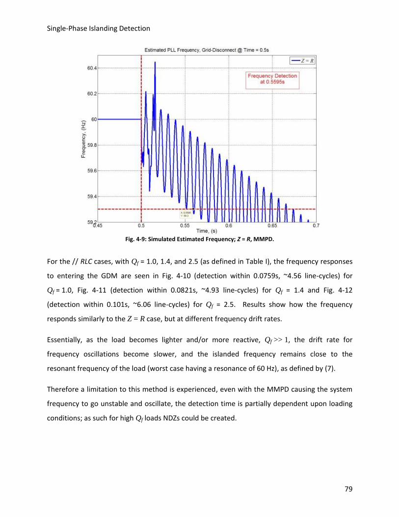
Single-Phase Islanding Detection
79
Fig. 4-9: Simulated Estimated Frequency; Z = R, MMPD.
For the // RLC cases, with Qf = 1.0, 1.4, and 2.5 (as defined in Table I), the frequency responses
to entering the GDM are seen in Fig. 4-10 (detection within 0.0759s, ~4.56 line-cycles) for
Qf = 1.0, Fig. 4-11 (detection within 0.0821s, ~4.93 line-cycles) for Qf = 1.4 and Fig. 4-12
(detection within 0.101s, ~6.06 line-cycles) for Qf = 2.5. Results show how the frequency
responds similarly to the Z = R case, but at different frequency drift rates.
Essentially, as the load becomes lighter and/or more reactive, Qf >> 1, the drift rate for
frequency oscillations become slower, and the islanded frequency remains close to the
resonant frequency of the load (worst case having a resonance of 60 Hz), as defined by (7).
Therefore a limitation to this method is experienced, even with the MMPD causing the system
frequency to go unstable and oscillate, the detection time is partially dependent upon loading
conditions; as such for high Qf loads NDZs could be created.

Single-Phase Islanding Detection
80
Fig. 4-10: Simulated Frequency; Z = RLC (Qf = 1.0), MMPD.
Fig. 4-11: Simulated Frequency; Z = RLC (Qf = 1.4), MMPD.
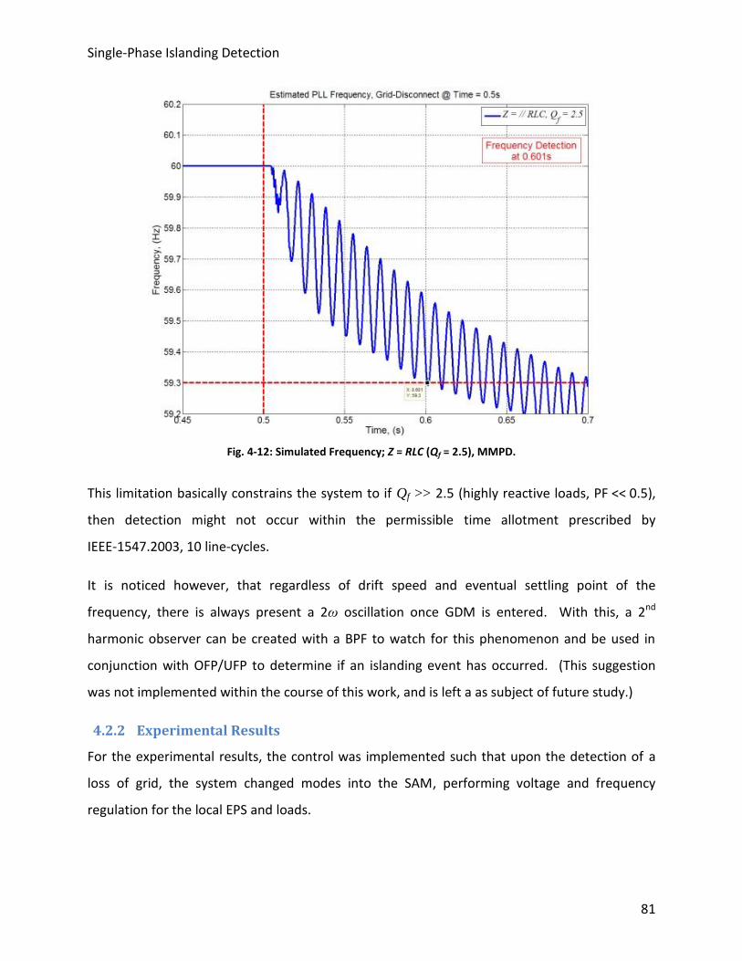
Single-Phase Islanding Detection
81
Fig. 4-12: Simulated Frequency; Z = RLC (Qf = 2.5), MMPD.
This limitation basically constrains the system to if Qf >> 2.5 (highly reactive loads, PF << 0.5),
then detection might not occur within the permissible time allotment prescribed by
IEEE-1547.2003, 10 line-cycles.
It is noticed however, that regardless of drift speed and eventual settling point of the
frequency, there is always present a 2ω oscillation once GDM is entered. With this, a 2nd
harmonic observer can be created with a BPF to watch for this phenomenon and be used in
conjunction with OFP/UFP to determine if an islanding event has occurred. (This suggestion
was not implemented within the course of this work, and is left a as subject of future study.)
4.2.2 Experimental Results
For the experimental results, the control was implemented such that upon the detection of a
loss of grid, the system changed modes into the SAM, performing voltage and frequency
regulation for the local EPS and loads.

Single-Phase Islanding Detection
82
The help enable a smooth transition from the GCM to the SAM, the grid voltage being tracked is
stored as the voltage reference for the SAM controller. Along with a rate-limiter that only
permits the voltage reference to change as fast as the dV/dt of the nominal grid voltage, allows
for a control system that smoothly changes from GCM to GDM. Once detection has occurred,
the PLL is disabled and the DCO is fed a constant reference frequency, as seen in Fig. 4-13.
Fig. 4-13: Enable/Disable Tracking function of PLL for constant frequency generation in SAM.
Starting with the simplest case to detect, seen in Fig. 4-14, the VSC is charging the DC link
batteries (at 500W), then a grid disconnection occurs; the control senses the disturbance and
changes the mode of operation within 1 line-cycle. Though this test is quite simple in terms of
detection, it presents the control with the toughest case for transient transition into the GDM:
full AC current phase reversal. Seen is how the control quickly, yet without sudden spikes or
distortions, regulates the voltage back to the nominal voltage and frequency.
The regenerative load tests in the following experimental cases use the values from Table I.
Results in Fig. 4-15, for a resistive load under load matching conditions, show the detection
time (~4 line-cycles after islanding event) and subsequent transition into a SAM once the
system enters into the GDM. As seen, the voltage transition is seamless from one mode to
another; thus the load continues on as if nothing even happened.

Single-Phase Islanding Detection
83
Fig. 4-14: Hardware Detection Response Time, Charging Batteries, MMPD.
Fig. 4-15: Hardware Detection Response Time, Z = R = 25Ω, MMPD.

Single-Phase Islanding Detection
84
Fig. 4-16: Hardware Detection Response Time, Z = RLC (Qf = 1.4), MMPD.
For the // RLC case, with Qf = 1.4, the results in Fig. 4-16 show that the control detects the
islanding event (within ~5.0 line-cycles) under load matching conditions, and while within the
specified amount of time, changes to SAM, and performs voltage and frequency regulation.
Similarly to the resistive case, the transition to SAM prevents the load from experiencing
downtimes or even quality issues. At the moment of transition into the SAM, it is seen that
there is a slight voltage distortion and current spike; this is accounted for in that the // RLC
loading in this case is more complex than simple resistors. Despite this, the transition is still
relatively smooth and seamless.
For all these cases, not only should the quick detection times be noted, but also the smooth
transition into the SAM and voltage and frequency regulation begun. This characteristic is
primarily enabled by the multiple-loop control architecture, with always active inner loop, and
the PLL setup and tracking of voltage reference for SAM during GCM.
The experimental detection times based upon OFP/UFP are summarized in Table III. Variances
between the simulated and experimental results can be attributed to model idealities,

Single-Phase Islanding Detection
85
controller discretization, and digital delay effects; as well as the relay turn on/off control delay
(variable between ½ to 1 line-cycle).
TABLE III: DETECTION TIMES FOR VARIOUS LOADING CASES
Loading Condition Islanding Time (Line-Cycles)
Simulated, R = 25Ω 3.57
Simulated, RLC, Qf = 1.0 4.56
Simulated, RLC, Qf = 1.4 4.93
Simulated, RLC, Qf = 2.5 6.06
Experimental, Charging. <1.0
Experimental, R ~4.0
Experimental, RLC, Qf = 1.4 ~5.0
Summarizing, it is found that under moderate Qf conditions, with relatively light loading, the
system was able to detect the islanding events and within the IEEE-1547.2003 specification of
10 line-cycles of an islanding event.

Resynchronization and Reclosure
86
5. Resynchronization and Reclosure
The two main concerns for reclosure of islanded systems to the grid are matching voltage
magnitude and phase between the Local/Area EPS and the restored grid. If the voltage
magnitude and/or phase alignment of the voltages between the islanded system and the utility
are not matched, then dangerously large (even catastrophic) transients can occur between the
systems via inrush effects.
Measurements
Grid
OK?
|V|
OK?
Freq
OK?
Phase
OK?
Stay
Islanded
Yes
Yes
Yes
Start
Reclosure
Yes
No
Fig. 5-1: Resynchronization Flowchart.
A simplified flowchart of a reclosure algorithm is seen in Fig. 5-1. It shows how as long as there
is a stable, disturbance-free grid voltage within nominal ranges, approximately equal voltage
magnitudes between the microgrid and grid, normal frequency ranges of the islanded system,
AND the phase angles between the microgrid and the grid are approximately equal, then it is
acceptable to reconnect the two systems.

Resynchronization and Reclosure
87
5.1 COMMON RECLOSURE METHODS
Methods of reconnecting to the grid post fault and/or islanding conditions can be classified into
two basic groups: De-energized and Energized. Each has advantages and disadvantages in
performance and complexity which will be discussed below.
5.1.1 De-energized Reclosure
De-energized methods of reclosing to the grid, as the name implies, requires an islanded
system to shut down and de-energize the Local/Area EPS(s) before true reconnection to the
grid can be made.
Generally, this is the safest means of reconnection, and being that for load systems that do not
contain local sources to sustain them during outages/faults, this is the standard method within
distribution systems that loads are reconnected to the grid (through relays and reclosures).
As one can imagine, this is not an optimal solution for microgrid operation. In this scheme,
loads and sources alike experience downtimes, and for critical loads that require backup,
downtimes can translate to millions of dollars lost (even for downtimes as short as a minute).
As such, this method of reconnection was explored, and energized, or “hot,” reclosures became
the focus.
5.1.2 Energized Reclosure
With energized reclosures to the grid, the source(s) of a Local/Area EPS remain up and running.
In this method of reconnecting to the grid, there are no downtimes, and transitions between
the modes of operation are generally minimized (via methods that follow the guidelines set
forth in Fig. 5-1.
Many methods of resynchronization and reclosure to the grid are performed in an OL manner.
Most common is a frequency drifting technique, in which a frequency offset of the islanded
system is added to the control system to speed up or slow down the AC voltage until it is
approximately aligned with the grid voltage. Alignment is performed via direct comparison of
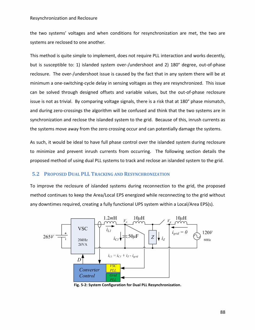
Resynchronization and Reclosure
88
the two systems’ voltages and when conditions for resynchronization are met, the two are
systems are reclosed to one another.
This method is quite simple to implement, does not require PLL interaction and works decently,
but is susceptible to: 1) islanded system over-/undershoot and 2) 180° degree, out-of-phase
reclosure. The over-/undershoot issue is caused by the fact that in any system there will be at
minimum a one-switching-cycle delay in sensing voltages as they are resynchronized. This issue
can be solved through designed offsets and variable values, but the out-of-phase reclosure
issue is not as trivial. By comparing voltage signals, there is a risk that at 180° phase mismatch,
and during zero-crossings the algorithm will be confused and think that the two systems are in
synchronization and reclose the islanded system to the grid. Because of this, inrush currents as
the systems move away from the zero crossing occur and can potentially damage the systems.
As such, it would be ideal to have full phase control over the islanded system during reclosure
to minimize and prevent inrush currents from occurring. The following section details the
proposed method of using dual PLL systems to track and reclose an islanded system to the grid.
5.2 PROPOSED DUAL PLL TRACKING AND RESYNCHRONIZATION
To improve the reclosure of islanded systems during reconnection to the grid, the proposed
method continues to keep the Area/Local EPS energized while reconnecting to the grid without
any downtimes required, creating a fully functional UPS system within a Local/Area EPS(s).
Fig. 5-2: System Configuration for Dual PLL Resynchronization.

Resynchronization and Reclosure
89
For this method of reconnection to the grid, multiple voltage sensors and PLL systems are
employed; a voltage sensor and a PLL for the EPS side of the grid connecting relay, and another
pairing for the grid side, as seen in Fig. 5-2.
Enabling of the PLLs to start resynchronization to the grid voltage and begin the transition
between the modes of operation, as described in Fig. 2-2, is as follows:
1. Sense that the grid voltage and frequency are stable and within nominal ranges;
2. Enable VSC PLL to begin tracking grid and send synthesized sine reference to voltage
controller (Fig. 5-3);
3. When frequency, phase, and magnitude of two systems confirmed to be within
acceptable tolerances, reclosure of the relay permitted;
4. Reclosure occurs and change in control modes via state-machine procedure in Fig. 2-2.
Fig. 5-3: Dual PLL Operation while system synchronizing.
In Fig. 5-4, the phase angles of the islanded and grid systems and the resynchronization
command are seen during the resynchronization process. The phase angles of the islanding
system and the grid are seen to come into alignment smoothly. The step response seen in the
figure shows the time at which the control has determined that the grid has returned and
initiates the resynchronization process. Noticed in the phase angle response of the VSC is how
once resynchronization is initialized, it quickly moves into phase alignment with the grid, then
overshoots, then re-corrects itself and ultimately achieves locked status with the grid PLL.

Resynchronization and Reclosure
90
Fig. 5-4: VSI and Grid Angles during Resynchronization.
The parameters in Table IV were used in the code to determine the moment of an acceptable
resynchronization level such that reclosure can commence. The values from Table IV were used
in a logical, rule-based fashion to determine if full resynchronization has occurred.
The flowchart in Fig. 5-5 outlines how the reclosure parameters are used; essentially, from the
two PLLs, the frequencies and phase angles are compared against the limits set forth by the
table, and if they are within the acceptable range, a counter is started. The counter must reach
1000 (three 60 Hz line-cycles assuming 20 kHz switching frequency) before the actual reclosure
process can begin. If at any time, the compared values violate the limit restrictions, the counter
is reset to zero. This allows for an enforcement of the three line-cycles of synchronized
operation before reclosure can take place.
TABLE IV: RECLOSURE PARAMETERS
Reclosure Parameter Value (Unit)
Δ|V| < 5% of Nominal (V)
ψ < 1 (degree)
Δω < 0.1 (Hz)
0.2 0.25 0.3 0.35 0.4 0.45 0.50
1
2
3
4
5
6
7
Time, (s)
VS
I a
nd
Grid
An
gle
s, (r
ad
/s)
VSI Angle
Grid Angle
Sync Start

Resynchronization and Reclosure
91
Fig. 5-5: Logic Flowchart for Synchronization Determination.
The waveforms in Fig. 5-6 show the Dual PLL system in action; as the EPS voltage tracks and
synchronizes with the grid voltage. The dynamics of the PLL are clearly shown as the EPS
voltage overshoots the grid voltage in the tracking process, but settles back into
synchronization shortly thereafter. Once synchronization is met, the voltage holds and
continues to track the grid voltage, waiting for reclosure process to occur.
Fig. 5-6: Resynchronization without reclosure.
Resynchronization and Reclosure
92
5.3 RECLOSURE CONTROL AND REFERENCE SELECTION
Once synchronization is complete, and the two systems are in phase-lock, the reclosure process
modifies the outer loop control to hold synchronization while reconnection takes place.
There are two basic ways that the outer loop controller can be operated during the reclosure
process and subsequent transition into GCM: 1) change to current mode then reclose, or 2) stay
in voltage mode, reclose, and then change into current mode.
5.3.1 Current Mode Control Pre-Reclosure
Change the outer loop’s mode to a constant current mode of operation (based off the current
reference generated by the AC voltage loop controller) before reclosure may seem like a simple
and ideal solution to avoid inrush currents during reclosure, but actually presents a wide-range
of issues and problems to overcome.
The implementation of tracking the AC current reference and freezing it for use as the constant
current reference is simple enough, but doing so leads to several secondary effects that need to
be considered. In a 1Φ system, when regulating the output current into the AC bus, the load
then dictates the voltage. As such, issues such as DC offsets generated in the AC voltage should
be considered.
In Fig. 5-7, the waveform shows the control system switching from AC voltage control to AC
current control before reconnection has occurred. Seen specifically is how a DC offset appears
in the AC voltage once the current mode of control is enabled. This offset can be accounted for
by capacitor-charge balance theory for the AC output filter cap for the VSC. Because the
balance is not being maintained cycle-by-cycle, the offset persists.
Other issues, such as load variation, should also be taken into account when considering how to
reclose to the grid. If the same approach to reclosure is taken as the previous example, voltage,
to current mode control, then reconnection, then as before, the load dictates the voltage while
constant current is applied. From this, if the current reference is already frozen, and the load
changes, then according to Ohm’s law, the voltage will change proportionally as well. This

Resynchronization and Reclosure
93
would require the voltage controller come back online and reestablish the correct current
reference to generate the nominal voltage, and hope that the load does not change again.
To take this type of iterative cycling and controller guesswork out of the system, it is therefore
much simpler to maintain voltage control during reclosure then quickly switch to the current
mode once reconnection has occurred.
Fig. 5-7: AC voltage w/ DC offset for reclosure process: Sync to Current Mode to Reclosure.
5.3.2 Current Mode Control Post-Reclosure
As mentioned, it is preferable to keep the outer AC voltage loop controller in effect during the
reclosure process to avoid issues caused by loading effects and variations. As such, a smoother
transition in the handling of the voltage is obtained.
There are concerns to be noted in this method of reclosure as well; mainly the selection of the
AC voltage reference to be used during the process. If the AC reference was continued to be
produced by PLL synthesis, as it is during the resynchronization process prior to the reclosure,
when the system reconnects, transients such as those in Fig. 5-8 are observed.

Resynchronization and Reclosure
94
Fig. 5-8: Resynchronization w/ reclosure and Vref = Fundamental from Grid PLL.
Fig. 5-9: Resynchronization w/ reclosure and Vref = Vgrid.

Resynchronization and Reclosure
95
These results in Fig. 5-8 specifically show how since the grid voltage is not a pure sinusoid,
when reconnection occurs the VSC tries to regulate the grid voltage to be purely sinusoidal.
Because the grid is vastly more dominant, the controller begins to windup and saturate with 3rd
order harmonic currents. This illustrates why it is necessary to not only have tight regulation of
the synchronization parameters, but also of the voltage itself.
To correct for this, once the systems are synchronized, the voltage reference for the outer loop
controller is changed from the fundamental synthesized from the PLL to that of the actual
measured grid voltage itself. Seen in Fig. 5-9, the response shows that before reclosure, the
VSC current to the microgrid is distorted to produce the necessary voltage. It also shows how
once the reclosure to the grid occurs, a minor transient in the current happens with negligible
impact on the voltage, and then continues on into a new GCM of operation. This tradeoff of
producing harmonic rich currents for a short period during reclosure is acceptable to avoid
controller saturation and ensure a smooth transition in the GCM.

Summary
96
6. Summary
6.1 CONCLUDING REMARKS
A control system for microgrid operation of DER/ES units was shown for grid-connected and
islanded modes, including the sub-modes of operation for each.
The controller’s architecture was selected to reduce transient effects between the changes in
the mode of operation and to provide current limiting capability to protect the system.
Simulations showed the transient performance between mode changes of the system, while
hardware results show stable operation in the steady-state conditions of each mode and the
transitions between them.
Stationary-frame PLL systems were developed that not only eliminate steady-state ripple errors
in the frequency generation, but increase performance through reduced settle times (faster
synchronization to input), without the need to add bulky LPFs to the system that would hurt the
performance of the PLL. The modifications to the PLL PD through phase angle feedback and
trigonometric manipulations were able to reduce ripple noise entirely under ideal conditions,
and by as much as 56.8% in extremely distorted cases. The modifications to the PLL LF via FFB
of the frequency error term showed improvements in synchronization speeds by over 50%.
Simulations and hardware results verify these improvements made by the modified methods.
Methods to mitigate the effects of amplitude mismatches in the PLL system were also discussed
and shown in simulations to increase the system performance, with the tradeoff being larger
overshoot in PLL frequency estimation during transient response times.
Islanding detection schemes were shown to incorporate PLL stability to create a quasi-active
islanding detection method that inherently becomes unstable for grid-disconnections. Analyses
and simulations show how these schemes sense for islanding conditions quickly and accurately
without having the constantly perturb the output to test of an islanding event through load
stability. Hardware results confirm the analyses and simulations, and test the proposed
method under IEEE-1547.2003 requirements to sense loss of grid events under load matching

Summary
97
conditions. Method yielded good results and met all requirements of the aforementioned
standard.
Resynchronization rules along with a method of how to properly reclose and change the mode
of operation back to the GCM were presented. Simulations show a smooth resynchronization
to the grid with little to no transient effects upon the voltage during reconnection. Hardware
tests confirm simulated results and showed how a seamless transfer back into a GCM can be
achieved from the loads’ point of view with minimal impact upon the system.
6.2 FUTURE WORK
The following items listed are left as future work to be continued:
Effects of LF modification to create adaptive control system
o Impact on PLL stability and resynchronization efforts
Synchronous Frame Control Implementation
o Implement a DQ control to eliminate steady-state errors
Synchronous Frame PLL Implementation for Islanding Detection
o DQ base PLL performance and stability analysis for use in Islanding Detection
Analysis of parallel systems operating within the Microgrid
o Stability during GCM of parallel systems using MMPD-based PLL Islanding
Detection
o Coordination between parallel resources to regulate a Microgrid in a stable
manner.
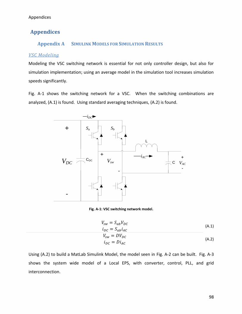
Appendices
98
Appendices
Appendix A SIMULINK MODELS FOR SIMULATION RESULTS
VSC Modeling
Modeling the VSC switching network is essential for not only controller design, but also for
simulation implementation; using an average model in the simulation tool increases simulation
speeds significantly.
Fig. A-1 shows the switching network for a VSC. When the switching combinations are
analyzed, (A.1) is found. Using standard averaging techniques, (A.2) is found.
CDC
L
C
+
VDC
-
iAC +
VAC
-
+
Vsw
-
iDC
Sa Sb
Fig. A-1: VSC switching network model.
(A.1)
(A.2)
Using (A.2) to build a MatLab Simulink Model, the model seen in Fig. A-2 can be built. Fig. A-3
shows the system wide model of a Local EPS, with converter, control, PLL, and grid
interconnection.
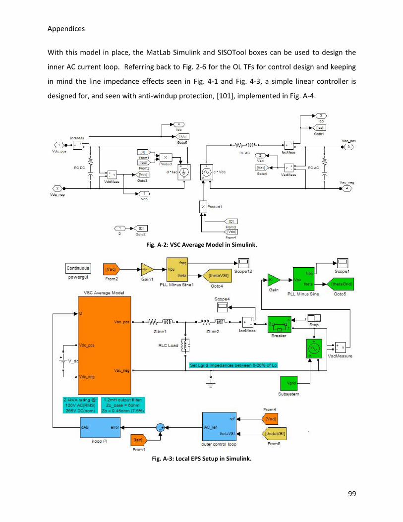
Appendices
99
With this model in place, the MatLab Simulink and SISOTool boxes can be used to design the
inner AC current loop. Referring back to Fig. 2-6 for the OL TFs for control design and keeping
in mind the line impedance effects seen in Fig. 4-1 and Fig. 4-3, a simple linear controller is
designed for, and seen with anti-windup protection, [101], implemented in Fig. A-4.
Fig. A-2: VSC Average Model in Simulink.
Fig. A-3: Local EPS Setup in Simulink.

Appendices
100
Fig. A-4: iAC control w/ Anti-Windup implementation.
(A.3)
Simulink Model for GCM – DC Current Control
Using the same structure as the Anti-Windup, PI regulator in Fig. A-4, the DC current controller
was designed with a low bandwidth (1-2 decades below AC current loop bandwidth). This is to
produce clean AC current reference signals and to track the desired DC current reference
accurately.
(A.4)
Simulink Model for GCM – AC Voltage Control
Using the same structure as the Anti-Windup, PI regulator in Fig. A-4, the AC Voltage controller
was designed with a bandwidth just above 60Hz. This is to produce clean AC current reference
signals and to generate a quality AC voltage for the loads to follow.
(A.5)

Appendices
101
Simulink Model for GCM – P/Q Control
Mathematical equations, as described from Section 2.4.2, were used to implement P/Q control.
Simulink blocks to implement this functionality are seen below.
(a)
(b)
(c)
Fig. A-5: DQ Transforms of 1Φ voltage.

Appendices
102
Fig. A-6: P/Q calculation of AC current reference using DQ voltage vector as Vpk.
Simulink Model for PLL Analysis
The block diagrams for each PLL implementation (for the modifications and testing) is seen in
Fig. A-7 – Fig. A-10 with the test setup for transient response to input steps seen in Fig. A-11.
Through the test setup, the steady-state and transient performance of each implementation
can be performed. The test setup shows how a step in the input signal can be done, and how
noise ripples to the input can be added.
Fig. A-7: SMPD PLL Implementation.

Appendices
103
Fig. A-8: SMPD w/ LPF Implementation.
Fig. A-9: MMPD PLL Implementation.
Fig. A-10: MMPD w/ FFB PLL Implementation.

Appendices
104
Fig. A-11: PLL Test Setup.
Simulink Model for Islanding Detection and Reclosure
The models below depict the control logic and outer loop controls for islanding detection and
reclosure. As noted in Chapters 4 and 5, these control functions reconfigure the outer loop
structure and PLL system to accommodate for the functionality they seek.
Fig. A-12: Islanding Detection Control Test Setup.
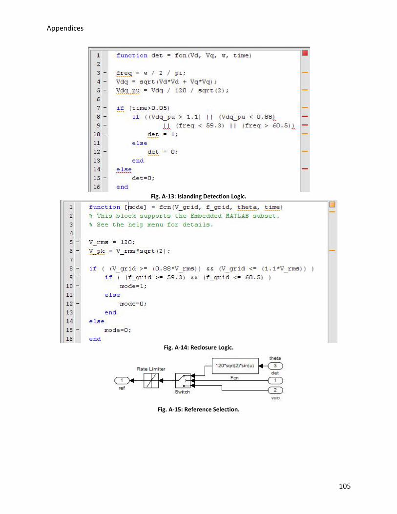
Appendices
105
Fig. A-13: Islanding Detection Logic.
Fig. A-14: Reclosure Logic.
Fig. A-15: Reference Selection.

Appendices
106
Appendix B HARDWARE SETUP FOR EXPERIMENTAL RESULTS
Broken into the key sections of hardware, the following sections describe and show the
hardware and control board setups.
The hardware used is a Vacon, Inc. motor drive (X4 20250 Series). Only the inverter and
auxiliary circuits of this drive are used, the remaining circuitry is deactivated. This commercial
motor drive was stripped of its control board and replaced with the following systems.
Universal Controller
The Universal Controller (UC), seen in Fig. B-1, is a multi-processor platform (FPGA and DSP
based) capable of handling all control functions necessary for this work. More information
about the UC can be found in the M.S.E.E. thesis of Mr. Gerald Francis, [102].
Modulation and protection schemes were implemented in the FPGA. More information and
coding pertaining to the FPGA can be found in the M.S.E.E. thesis of Mr. Arman Roshan, [103].
Higher level control functions were implemented in DSP code, and can be found in Appendix C.
FPGA
DSP
Bo
ot N
VR
AM
Lo
we
r
Mu
ltipro
ce
csso
r
Co
nn
ecto
r
Lo
we
r
Mu
ltipro
ce
csso
r
Co
nn
ecto
r
FPGA
Configuration
PROM
DATA[63...0]
ADDR[31...0]
PDATA[31...0]
PADDR[18...0]
Glo
ba
l
Intre
rface
NV
RA
M
DA
C
DIP
Sw
itch
es
PM
C
HE
X D
isp
lay
PMC Bus
Connectors
Expansion
I/OTransceivers
Fig. B-1: Universal Controller.

Appendices
107
Analog-to-Digital Board
The Analog-to-Digital (A/D) conversion board was developed at the Center for Power
Electronics Systems (CPES) at Virginia Tech. It contains LEM voltage sensors, as well as inputs
for other miscellaneous sensor inputs, noise filtering, and 12 bit resolution A/D chips from
Analog Devices.
For this work, some sensed signals come from the drive itself (DC voltage and AC current).
These values are processed on the Interface Board (described in the following section), then fed
directly into the A/D chips.
Circuit schematics for this board accompany this dissertation in the form of separate PDF files.
Co
nn
ecto
r to In
terfa
ce
Co
nn
ecto
r to
UC
Power
A/D
External Connector
Fitle
ring
LEMs
Fig. B-2: Analog-to-Digital Control Board.

Appendices
108
Drive Interface Board
The Drive Interface Board was developed to interface the UC and A/D boards to the drive itself.
This board contains not only pin routing but hardware protection features as well. In the event
that system current or voltage exceeds safe operating conditions, the gate drives are
automatically disabled on this board.
Protection is implemented via user-set, level comparisons with the sensed variables before A/D
conversion is made.
Scaling and routing of sensed variable from the drive (as mentioned previously) are performed
here as well.
Circuit schematics for this board accompany this dissertation in the form of separate PDF files.
Co
nn
ecto
r to D
rive
Protection
Comparison
Gate-Drives
Co
nn
ecto
r to
UC
& A
/D
Power
Variable
Scaling
Fig. B-3: Drive Interface Board.

Appendices
109
Battery System
The batteries used in the experimentations were large format, Nickel Metal-Hydride (Ni-MH)
cells from Nilar (http://www.nilar.com/). Eleven 24V, 9A-hr cells in series created a 264V,
2.3kW-hr battery system.
This system was connected to the VSC (as seen in the following section) DC link via an inductive
choke. The battery system also contains fuses and a 500V, 25A DC breaker.
Fig. B-4: Ni-MH Battery System with DC circuit breaker and fuses.
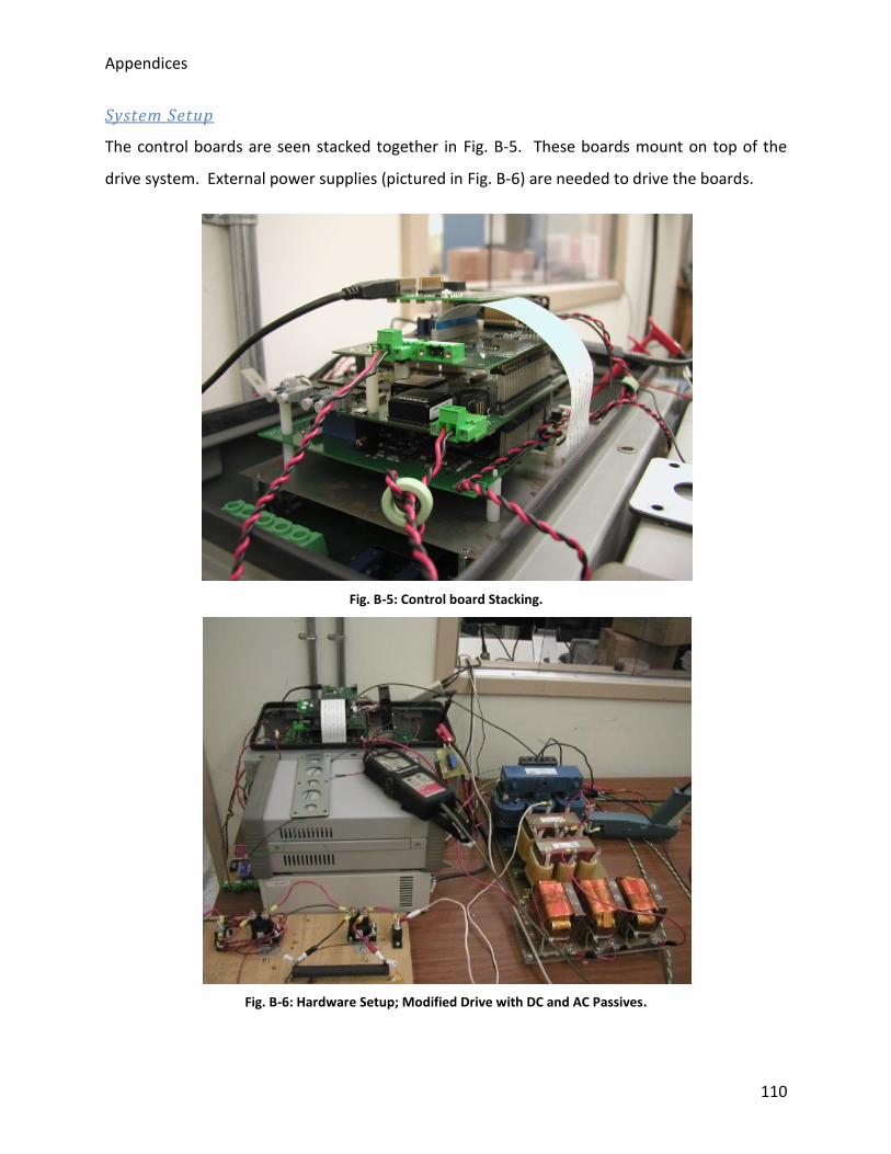
Appendices
110
System Setup
The control boards are seen stacked together in Fig. B-5. These boards mount on top of the
drive system. External power supplies (pictured in Fig. B-6) are needed to drive the boards.
Fig. B-5: Control board Stacking.
Fig. B-6: Hardware Setup; Modified Drive with DC and AC Passives.

Appendices
111
The complete hardware setup (excluding the batteries) is seen in Fig. B-6. In the figure, the
converter, with associated control power supplies are seen to the left, as well as the AC and DC
link inductors and capacitors on the right. In the bottom left are the DC link pre-charge circuit
and PCC relays.

Appendices
112
Appendix C DSP CODE FOR MODES OF OPERATION
Islanding Detection Code
#include <sysreg.h>
#include <def21160.h>
#include <math.h>
#include <signal.h>
#include <stdio.h>
#include <stdlib.h>
#include <21160.h>
#include "UControl.h"
#include "Parameters.h"
#include "functions.h"
void Ramp_vref(float);
void Input_filter(void);
void Vdc_PI_Comp(void);
void Iac_PI_Comp(void);
void De_sat(void);
void Ramp_iref(void);
//void maindd(void){while(1){}};
//Parameter array that interacts with USB
extern int g_nParamArray[15];
//////////////////////////////////////////////////////////////////////////////////
// <SUMMARY>Write a value to the hex display. </SUMMARY>
inline void HexWrite( const unsigned int nVal ){
*(volatile UINT*)(0x0A000000) = nVal;
}
UINT g_nCurrPkt1Prev;
UINT g_nNextActivation;
/// <SUMMARY>Read data from FPGA memory</SUMMARY>
/// <REMARKS>This function is used to read data from the FPGA and includes the timing
/// delay necessary to prevent deadlock.</REMARKS>
/// <PARAM name="nAddr">This is the address of the FPGA memory location to read.</PARAM>
//#pragma pure
unsigned int FPGARead( const unsigned int nAddr ){
asm("nop;");
volatile unsigned int* pInt = (unsigned int*)(nAddr);
unsigned int nRet = 0;
nRet = *pInt;
asm("nop;");
return nRet;
}
/// <SUMMARY>Write data to the FPGA</SUMMARY>
/// <PARAM name="nAddr">Target address to write to.</PARAM>
/// <PARAM name="nVal">Value to write to the address</PARAM>
void FPGAWrite( const unsigned int nAddr, const unsigned int nVal ){
asm("nop;");
volatile unsigned int* pInt = (unsigned int*)(nAddr);
*pInt = nVal;
asm("nop;");
}
/// <SUMMARY>Delay process used to wait in the DSP.</SUMMARY>
/// <PARAM name="nMaxCtr">This is a counter that indicates how many wait loops should
execute.</PARAM>
#pragma const
void DelayProc(const unsigned int nMaxCtr){
unsigned int n;
for( n = 0; n < nMaxCtr; n++ ){
asm("nop;");
asm("nop;");
asm("nop;");

Appendices
113
}
}
//////////////////////////////////////////////////////////////////////////////////
/// <SUMMARY>Write to USB device and do not assert ackstat. </SUMMARY>
void USBWrite( const UINT nReg, const UINT nValue, const UINT nMarker ){
UINT nOutVal = nMarker & 0xFFFF0000;
UINT nCmd = ((nReg << 3))&0xF8; //mask address
nCmd = nCmd | 0x02; //write
nOutVal = nOutVal | (nCmd << 8 );
nOutVal = nOutVal | (nValue & 0xFF );
FPGAWrite( 0x14000000, nOutVal );
}
//////////////////////////////////////////////////////////////////////////////////
/// <SUMMARY>Write to USB device and assert ackstat. </SUMMARY>
void USBWriteAS( const UINT nReg, const UINT nValue, const UINT nMarker ){
UINT nOutVal = nMarker & 0xFFFF0000;
UINT nCmd = ((nReg << 3))&0xF8; //mask address
nCmd = nCmd | 0x02; //write
nCmd = nCmd | 0x01; //Enable ACKSTAT
nOutVal = nOutVal | (nCmd << 8 );
nOutVal = nOutVal | (nValue & 0xFF );
FPGAWrite( 0x14000000, nOutVal );
}
//////////////////////////////////////////////////////////////////////////////////
/// <SUMMARY>Read USB register and do not set acknowledge bit.</SUMMARY>
void USBRead( const UINT nReg, const UINT nMarker ){
UINT nOutVal = nMarker & 0xFFFF0000;
const UINT nCmd = ((nReg << 3)&0xF8); //mask address
nOutVal = nOutVal | (nCmd << 8 );
FPGAWrite( 0x14000000, nOutVal );
}
//////////////////////////////////////////////////////////////////////////////////
/// <SUMMARY>Read USB register and set acknowledge bit.</SUMMARY>
void USBReadAS( const UINT nReg, const UINT nMarker ){
UINT nOutVal = nMarker & 0xFFFF0000;
UINT nCmd = ((nReg << 3)&0xF8); //mask address
nCmd = nCmd | 0x01; //Enable ACKSTAT
nOutVal = nOutVal | (nCmd << 8 );
FPGAWrite( 0x14000000, nOutVal );
}
void mainUSB(void);
void UpdateUSBParameters(){
g_nParamArray[0]=MODE_STATUS;
g_nParamArray[1]=*(int*)(&ACTIVE_POWER);
g_nParamArray[2]=*(int*)(&REACTIVE_POWER);
g_nParamArray[3]=Batt_SOC;
//g_nParamArray[3]=Iac_ref;
//MODE_DEMAND=g_nParamArray[4];
P_DEMAND=*(int*)(&g_nParamArray[5]);
Q_DEMAND=*(int*)(&g_nParamArray[6]);
VOLTAGE=g_nParamArray[7];
FREQ=g_nParamArray[8];
g_nParamArray[11] = GRID_MODE;
Dump_Mem = g_nParamArray[12];
//GRID_MODE = g_nParamArray[11];
//PF_Multiplier = g_nParamArray[12];
//DC_Current_Command = g_nParamArray[4];

Appendices
114
}
int main()
{
sysreg_bit_set(sysreg_MODE2, IRQ0E); //enable /IRQ0
sysreg_bit_clr(sysreg_MODE1, IRPTEN);
//////////////////////////////////////////////////////
*g_cpwDACCTL = 0x00000003; // Initialization of DAC
*g_cpwDACCTL = 0x00000002; // Initialization of DAC
*g_cpwDACCTL = 0x00000003; // Initialization of DAC
/////////////////////////////////////////////////////
ConfigurePWM(); //send out the first data
interrupt (SIG_IRQ0,irq0_handler); //Interrupt
// sysreg_bit_clr(sysreg_MODE1, IRPTEN); //enable global interrupt
while(1){
asm("nop;");
asm("nop;");
asm("nop;");
//USB Main function
mainUSB();
//maindd();
}
}
void ConfigurePWM()
{
*g_cpwPer = bitPer; // Switching Period expressed in clock cycles Tsw/
12.5ns
*g_cpwDeadtime = 100; // Deadtime expressed in clock cycles 1us/
12.5ns
*g_cpwPD = 100; // Pulse Deletion expressed in clock cycles 0/ 12.5ns
*g_cpwDuty = 0.2*bitPer;
*g_cpwMod_SEL = 1; // when 1 Unipolar, When 0 Bipolar
*g_cpwCurr_Dir = 0; // Current Direction used for deadtime compensation
*reset_ff = 1; // reset D flipflop
*reset_ff2 = 1; // reset D flipflop
*reset_ff3 = 1; // reset D flipflop
*relay = 1; // reset relay
// *HSFan = 0; // reset HSFan
*g_cpwDeadCom = DTC_OnOff; //reset deadtime compensation
}
///////////////////////////////////////////////////////////////////
//AD data read out
void ADScale()
{
float IL_Temp;
float Vdc_Temp;
float Vac_Temp;
float Vacg_Temp;
float HS_Temp;
int ADC_CHA= *reg_ADC2CHA;
int ADC_CHB= *reg_ADC1CHB;
int ADC_CHC= *reg_ADC2CHC;
int ADC_CHD= *reg_ADC1CHA;
//converting 2's compliments to float
//-------------------------------
if(ADC_CHA >= 0x800)
IL_Temp = (-(~(ADC_CHA-1) & 0xfff)+CHC1_CHA_OFFSET)/CHC1_CHA_SCALE;
else
IL_Temp = (ADC_CHA+CHC1_CHA_OFFSET)/CHC1_CHA_SCALE;

Appendices
115
//-------------------------------
//-------------------------------
if(ADC_CHB >= 0x800)
Vac_Temp = (-(~(ADC_CHB-1) & 0xfff)+CHC1_CHB_OFFSET)/CHC1_CHB_SCALE;
else
Vac_Temp = (ADC_CHB+CHC1_CHB_OFFSET)/CHC1_CHB_SCALE;
//-------------------------------
//-------------------------------
if(ADC_CHC >= 0x800)
Vdc_Temp = (-(~(ADC_CHC-1) & 0xfff)+CHC2_CHA_OFFSET)/CHC2_CHA_SCALE;
else
Vdc_Temp = (ADC_CHC+CHC2_CHA_OFFSET)/CHC2_CHA_SCALE;
//-------------------------------
/*
//-------------------------------
if(ADC_CHD >= 0x800)
Charge_I = (-(~(ADC_CHD-1) & 0xfff)+CHC2_CHB_OFFSET)/CHC2_CHB_SCALE;
else
Charge_I = (ADC_CHD+CHC2_CHB_OFFSET)/CHC2_CHB_SCALE;
//-------------------------------
*/
//-------------------------------
if(ADC_CHD >= 0x800)
Vacg_Temp = (-(~(ADC_CHD-1) & 0xfff)+CHC2_CHB_OFFSET)/CHC2_CHB_SCALE;
else
Vacg_Temp = (ADC_CHD+CHC2_CHB_OFFSET)/CHC2_CHB_SCALE;
//-------------------------------
Iac = ( IL_Temp - (0.152463) ) * (21.2);// - (3.0*0.299497496); //
Setting the polarity right
Vac = ( Vac_Temp + 0.009 ) * (22.9) *(1.0);
Vac_grid = ( Vacg_Temp + 0.009 ) * (22.9) *(1.0);
Vdc = ( Vdc_Temp + 8.0235 ) * (27.205);
// Charge_I = Charge_I * (1000/328.0);
}
/////////////////////////////////////////////////////////////////////////////////////////////////
///////////////////
//interrupt routine
void irq0_handler(int useless)
{
while(*reg_ADAV==0)
asm("nop;");
//////////////////
ADScale();
//////////////////
// Protection();
//////////////////
///////////////////////////////////////////////////////////
Open_Close_Sel=0;
if (Open_Close_Sel==1)
Openloop(); //openloop control
else if (Open_Close_Sel==0)
{
Closedloop(); //closedloop control
Duty = (bitPer * 0.5) + (bitPer * 0.5) * Duty_ab; //transfer to counter number
// Duty=0;
}
////////////////////////////////////////////////////////////
if(Iac>0) //determine current direction
Curr_Dir=1;
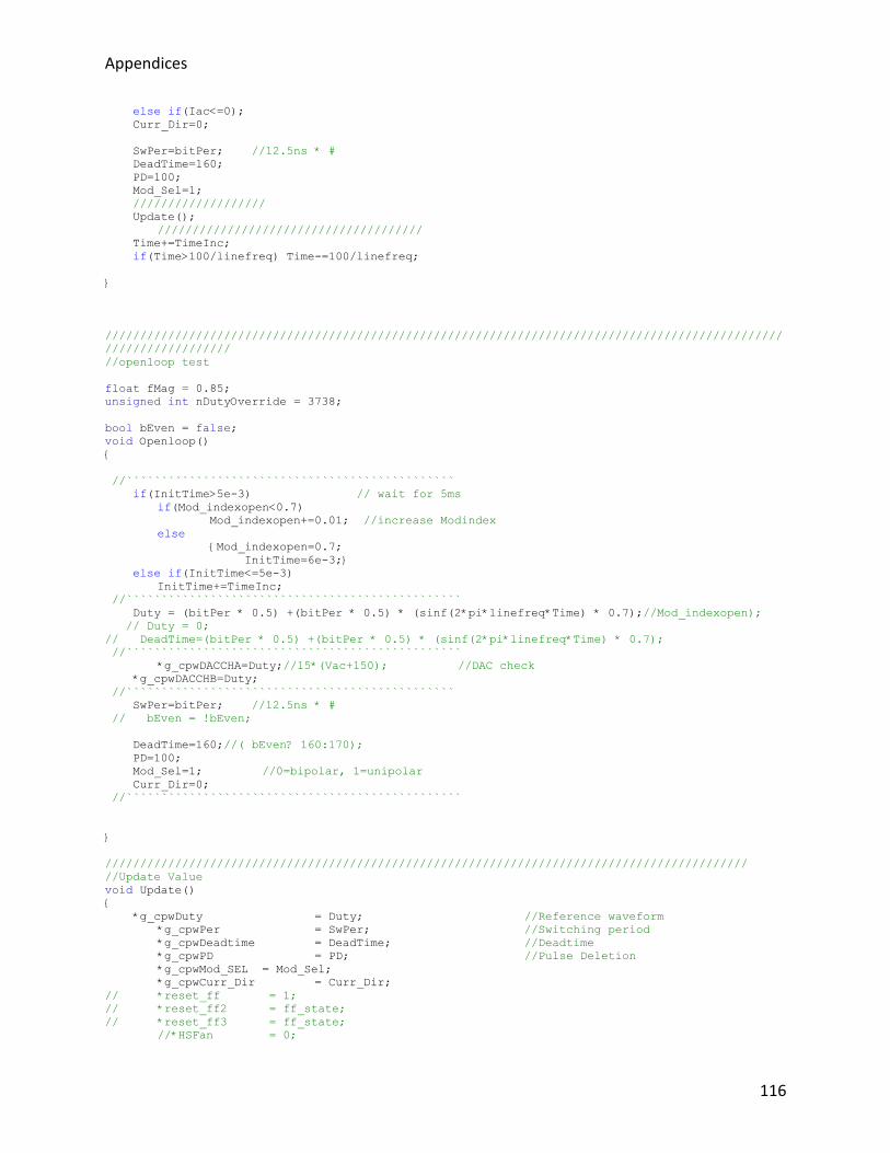
Appendices
116
else if(Iac<=0);
Curr_Dir=0;
SwPer=bitPer; //12.5ns * #
DeadTime=160;
PD=100;
Mod_Sel=1;
///////////////////
Update();
//////////////////////////////////////
Time+=TimeInc;
if(Time>100/linefreq) Time-=100/linefreq;
}
/////////////////////////////////////////////////////////////////////////////////////////////////
//////////////////
//openloop test
float fMag = 0.85;
unsigned int nDutyOverride = 3738;
bool bEven = false;
void Openloop()
{
//```````````````````````````````````````````````
if(InitTime>5e-3) // wait for 5ms
if(Mod_indexopen<0.7)
Mod_indexopen+=0.01; //increase Modindex
else
{Mod_indexopen=0.7;
InitTime=6e-3;}
else if(InitTime<=5e-3)
InitTime+=TimeInc;
//````````````````````````````````````````````````
Duty = (bitPer * 0.5) +(bitPer * 0.5) * (sinf(2*pi*linefreq*Time) * 0.7);//Mod_indexopen);
// Duty = 0;
// DeadTime=(bitPer * 0.5) +(bitPer * 0.5) * (sinf(2*pi*linefreq*Time) * 0.7);
//````````````````````````````````````````````````
*g_cpwDACCHA=Duty;//15*(Vac+150); //DAC check
*g_cpwDACCHB=Duty;
//```````````````````````````````````````````````
SwPer=bitPer; //12.5ns * #
// bEven = !bEven;
DeadTime=160;//( bEven? 160:170);
PD=100;
Mod_Sel=1; //0=bipolar, 1=unipolar
Curr_Dir=0;
//````````````````````````````````````````````````
}
////////////////////////////////////////////////////////////////////////////////////////////
//Update Value
void Update()
{
*g_cpwDuty = Duty; //Reference waveform
*g_cpwPer = SwPer; //Switching period
*g_cpwDeadtime = DeadTime; //Deadtime
*g_cpwPD = PD; //Pulse Deletion
*g_cpwMod_SEL = Mod_Sel;
*g_cpwCurr_Dir = Curr_Dir;
// *reset_ff = 1;
// *reset_ff2 = ff_state;
// *reset_ff3 = ff_state;
//*HSFan = 0;
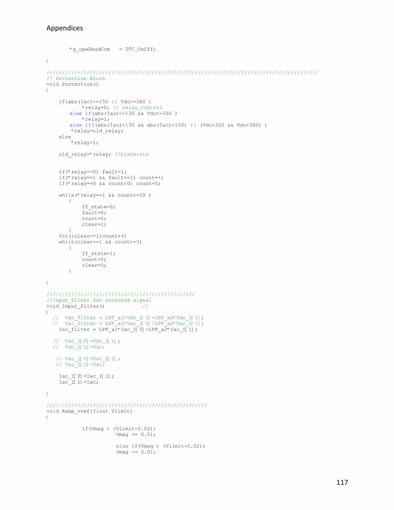
Appendices
117
*g_cpwDeadCom = DTC_OnOff;
}
////////////////////////////////////////////////////////////////////////////////////////
// Protection Block
void Protection()
{
if(abs(Iac)>=150 || Vdc>=380 )
*relay=0; // relay_control
else if(abs(Iac)<=130 && Vdc<=350 )
*relay=1;
else if((abs(Iac)>130 && abs(Iac)<150) || (Vdc>350 && Vdc<380) )
*relay=old_relay;
else
*relay=1;
old_relay=*relay; //histersis
if(*relay==0) fault=1;
if(*relay==1 && fault==1) count++;
if(*relay==0 && count>0) count=0;
while(*relay==1 && count>=50 )
{
ff_state=0;
fault=0;
count=0;
clear=1;
}
for(;clear==1;count++)
while(clear==1 && count>=3)
{
ff_state=1;
count=0;
clear=0;
}
}
////////////////////////////////////////////////
//Input_filter for sensored signal
void Input_filter() //
{
// Vdc_filter = LPF_a1*Vdc_I[0]+LPF_a2*Vdc_I[1];
// Vac_filter = LPF_a1*Vac_I[0]+LPF_a2*Vac_I[1];
Iac_filter = LPF_a1*Iac_I[0]+LPF_a2*Iac_I[1];
// Vdc_I[0]=Vdc_I[1];
// Vdc_I[1]=Vdc;
// Vac_I[0]=Vac_I[1];
// Vac_I[1]=Vac;
Iac_I[0]=Iac_I[1];
Iac_I[1]=Iac;
}
////////////////////////////////////////////////////
void Ramp_vref(float Vlimit)
{
if(Vmag < (Vlimit-0.02))
Vmag += 0.01;
else if(Vmag > (Vlimit+0.02))
Vmag -= 0.01;

Appendices
118
else
Vmag = Vlimit;
}
//////////////////////////////////////////////////
//////////////////////////////////////////////////
void Ramp_Ref(float* pMagRef, float pMagCmd, float RampStep)
{
//if ref command (minus 0.02) is > present ref, increase by 0.01 until condition met
if( *pMagRef < (pMagCmd - 2*RampStep) ){
*pMagRef += RampStep;
}
//else if ref command (plus 0.02) is < present ref, decrease by 0.01 until condition met
else if ( *pMagRef > (pMagCmd + 2*RampStep) ){
*pMagRef -= RampStep;
}
//otherwise, ramped reference has reached commanded reference so set reference to
commanded reference
else{
*pMagRef = pMagCmd;
}
}
///////////////////////////////////////////////////
//////////////////////////////////////////////////
void Isl_Detect(const float pVd, const float pVq, const float w_PLL, bool* pGridOk, bool
Remote_GridOk)
{
const float Vdq = sqrt(pVd*pVd + pVq*pVq);
const float f_line = w_PLL / twopi;
if ( *pGridOk == true ){
if ( (Vdq >= 0.88*Vnom1) && (Vdq <= 1.1*Vnom1) && (f_line >= 59.3) && (f_line <= 60.5) ){
*pGridOk = true;
}
else{
*pGridOk = false;
}
}
else{
if (Remote_GridOk == true){
*pGridOk = true;
}
else{
*pGridOk = false;
}
}
}
///////////////////////////////////////////////////
///////////////////////////////////////////////////
void DQ_TransformV(const float Va, const float w_PLLv, float* pVd, float* pVq)
{
float dVy, dVz;
Valpha = Va;
dVz = w_PLLv*Valpha;
dVy = (Vz - Valpha - Vy)*w_PLLv;
Vz = Vz + Period*dVz;
Vy = Vy + Period*dVy;
Vbeta = Vz - Valpha - Vy;
//Modified, sine-based DQ (Park's) Transform
*pVd = Valpha*sin_theta - Vbeta*cos_theta;// + 0.8;
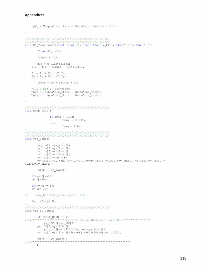
Appendices
119
*pVq = Valpha*cos_theta + Vbeta*sin_theta;// + 2.5;
}
///////////////////////////////////////////////////
///////////////////////////////////////////////////
void DQ_TransformI(const float Ia, const float w_PLLi, float* pId, float* pIq)
{
float dIy, dIz;
Ialpha = Ia;
dIz = w_PLLi*Ialpha;
dIy = (Iz - Ialpha - Iy)*w_PLLi;
Iz = Iz + Period*dIz;
Iy = Iy + Period*dIy;
Ibeta = Iz - Ialpha - Iy;
//DQ (Park's) Transform
*pId = Ialpha*sin_theta - Ibeta*cos_theta;
*pIq = Ialpha*cos_theta + Ibeta*sin_theta;
}
///////////////////////////////////////////////////
void Ramp_iref()
{
if(Imag < 1.98)
Imag += 0.001;
else
Imag = 2.0;
}
///////////////////////////////////////////////////
///////////////////////////////////////////////////
void Vac_Comp()
{
yv_inv[2]=yv_inv[1];
yv_inv[1]=yv_inv[0];
xv_inv[2]=xv_inv[1];
xv_inv[1]=xv_inv[0];
xv_inv[0]=Vac_err;
yv_inv[0]=0.1*(xv_inv[0]+0.1799*xv_inv[1]-0.8201*xv_inv[2])+1.2953*yv_inv[1]-
0.2953*yv_inv[2];
yv[0] = yv_inv[0];
if(yv[0]>=30)
yv[0]=30;
if(yv[0]<=-30)
yv[0]=-30;
// Ramp_Ref(&Iac_refx, yv[0], 1.0);
Iac_refx=yv[0];
}
///////////////////////////////////////////////////
void Vdc_PI_Comp()
{
if (GRID_MODE == 0){
////*********************current charge/discharge controller****************
yv_iDC[3]=yv_iDC[2];
yv_iDC[1]=yv_iDC[0];
yv_iDC[2]=1.4721/2*Vac_err+yv_iDC[3];
yv_iDC[0]=yv_iDC[2]*50e-6+(1-96.3*50e-6)*yv_iDC[1];
yv[0] = yv_iDC[0];
////************************************************************
}

Appendices
120
else if (GRID_MODE == 1){
////**********************AC voltage inverter test*************************
yv_inv[2]=yv_inv[1];
yv_inv[1]=yv_inv[0];
xv_inv[2]=xv_inv[1];
xv_inv[1]=xv_inv[0];
xv_inv[0]=Vac_err;
yv_inv[0]=0.1*(xv_inv[0]+0.1799*xv_inv[1]-0.8201*xv_inv[2])+1.2953*yv_inv[1]-
0.2953*yv_inv[2];
yv[0] = yv_inv[0];
////************************************************************
}
else if (GRID_MODE == 2){
////***********************************DC voltage rectifier test***************
yv_rec[3]=yv_rec[2];
yv_rec[1]=yv_rec[0];
xv_rec[1]=xv_rec[0];
xv_rec[0]=Vac_err;
yv_rec[2]=xv_rec[0]+(13.7*50e-6-1)*xv_rec[1]-(30.5*50e-6-1)*yv_rec[3];
yv_rec[0]=20*50e-6*yv_rec[2]+yv_rec[1];
yv[0] = yv_rec[0];
////**************************************************************
}
else{
yv[0] = 0;
}
if(yv[0]>=30)
yv[0]=30;
if(yv[0]<=-30)
yv[0]=-30;
Iac_refx=yv[0];
}
////////////////////////////////////////////////////
void PLL()
{
Err_PLL = (Vac/Vnom1)*cos_theta - sin_theta*cos_theta;
//Vnom = 100 Vrms
//Vnom1 = 120 Vrms
Int_Vac_PLL = Int_Vac_PLL + Ki_PLL*Err_PLL*Period;
Pro_Vac_PLL = Kp_PLL*Err_PLL;
w = Int_Vac_PLL + Pro_Vac_PLL + twopi*linefreq;
// equivalent if/else statements for upper and lower frequency limits on PLL
w = ( (w <= twopi*flimit_hPLL) ? w : (twopi*flimit_hPLL) );
w = ( (w >= twopi*flimit_lPLL) ? w : (twopi*flimit_lPLL) );
if (GRID_MODE == 1){
w = twopi*linefreq;
}
theta = theta + w*Period;
if (theta > twopi){
theta -= twopi;
}
else if (theta < 0.0){
theta += twopi;
}
cos_theta = cosf(theta);
sin_theta = sinf(theta);
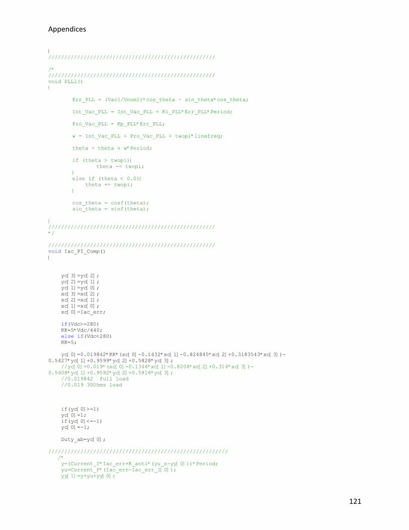
Appendices
121
}
////////////////////////////////////////////////////
/*
////////////////////////////////////////////////////
void PLL1()
{
Err_PLL = (Vac1/Vnom1)*cos_theta - sin_theta*cos_theta;
Int_Vac_PLL = Int_Vac_PLL + Ki_PLL*Err_PLL*Period;
Pro_Vac_PLL = Kp_PLL*Err_PLL;
w = Int_Vac_PLL + Pro_Vac_PLL + twopi*linefreq;
theta = theta + w*Period;
if (theta > twopi){
theta -= twopi;
}
else if (theta < 0.0){
theta += twopi;
}
cos_theta = cosf(theta);
sin_theta = sinf(theta);
}
////////////////////////////////////////////////////
*/
////////////////////////////////////////////////////
void Iac_PI_Comp()
{
yc[3]=yc[2];
yc[2]=yc[1];
yc[1]=yc[0];
xc[3]=xc[2];
xc[2]=xc[1];
xc[1]=xc[0];
xc[0]=Iac_err;
if(Vdc>=280)
KK=5*Vdc/440;
else if(Vdc<280)
KK=5;
yc[0]=0.019842*KK*(xc[0]-0.1432*xc[1]-0.824845*xc[2]+0.3183543*xc[3])-
0.5427*yc[1]+0.9599*yc[2]+0.5828*yc[3];
//yc[0]=0.019*(xc[0]-0.1344*xc[1]-0.8204*xc[2]+0.314*xc[3])-
0.5408*yc[1]+0.9592*yc[2]+0.5816*yc[3];
//0.019842 full load
//0.019 30Ohms load
if(yc[0]>=1)
yc[0]=1;
if(yc[0]<=-1)
yc[0]=-1;
Duty_ab=yc[0];
////////////////////////////////////////////////////////
/*
y=(Current_I*Iac_err+K_anti*(yu_s-yy[0]))*Period;
yu=Current_P*(Iac_err-Iac_err_I[0]);
yy[1]=y+yu+yy[0];

Appendices
122
if(abs(yy[1])<=1) yu_s=yy[1];
else if(yy[1]>1) yu_s=1;
else if(yy[1]<-1) yu_s=-1;
yy[0]=yy[1];
Iac_err_I[0]=Iac_err; //update
Duty_ab=yy[1];
*/
////////////////////////////////////////
/*
y_delta=Current_I*Iac_err*Period;
y+=y_delta;
yu=Current_P*Iac_err;
yy=y+yu;
if ( yy > 1 )
{
yy = 1;
y -= 1*y_delta; //Stop integral when saturation
}
else if ( yy < -1 )
{
yy = -1;
y -= 1*y_delta; //Stop integral when saturation
}
Duty_ab=yy;
*/
///////////////////////////////////////////
/*
Iac_err_I[0]=Iac_err_I[1]; //update
Iac_err_I[1]=Iac_err;
Dab[1]=(a1 * Iac_err_I[1]) + (a2 * Iac_err_I[0]) + Dab[0]; //PI
Dab[0]=Dab[1]; //update
//Iac_err_I[0]=Iac_err_I[1]; //update
//Iac_err_I[1]=Iac_err;
float fscale = fabs(Dab[1]);
if(fscale >= 0.9){
float fscaleinv = 1.0/fscale;
Dab[1] *= fscaleinv;
Dab[0] *= fscaleinv;
}
Duty_ab=Dab[1];
*/
///////////////////////////////////////////
}
///////////////////////////////////////////////////
////////////////////////////////////////////////////
//saturation limit for Duty cycle
void De_sat()
{
if (Duty_ab>=1)
Duty_ab=1;
else if (Duty_ab<=-1)
Duty_ab=-1;
}
///////////////////////////////////////////////////
///////////////////////////////////////////////////
void ChargeCurrentRef()
{

Appendices
123
if (Vdc <= 306.0){
I_DCref = 6.0;
Charge_flag=0;
}
else if ((Vdc <= 308.0) && Charge_flag==0 && StopCharge_flag==0){
I_DCref = 6.0;
}
else if (Vdc <= 312.2 && Charge_flag1==0 && StopCharge_flag==0){
Charge_flag=1;
I_DCref = 3.0;
Charge_flag1=0;
}
else if ((Vdc <= 314.2) && Charge_flag1==0 && StopCharge_flag==0){
I_DCref = 3.0;
}
else if (Vdc <= 322.2 && Charge_flag2==0 && StopCharge_flag==0){
Charge_flag1=1;
I_DCref = 2.5;
Charge_flag2=0;
}
else if ((Vdc <= 316.0) && Charge_flag2==0 && StopCharge_flag==0){
I_DCref = 2.5;
}
else if (Vdc <= 317.0){
Charge_flag2=1;
I_DCref = 1.0;
Charge_flag3=0;
}
else if ((Vdc <= 326.0) && Charge_flag3==0 && StopCharge_flag==0){
I_DCref = 1.0;
}
else if (Vdc <= 327.0 && StopCharge_flag==0){
Charge_flag3=1;
I_DCref = 0.3;
StopCharge_flag=0;
}
else if ((Vdc < 328.0) && StopCharge_flag==0){
I_DCref = 0.3;
}
else if ((Vdc <= 330.0)){
I_DCref = 0.0;
StopCharge_flag = 1;
}
else{
I_DCref = 0.0;
StopCharge_flag = 1;
}
}
///////////////////////////////////////////////////
///////////////////////////////////////////////////
void StateOfCharge()
{
// SOC 0 - 60
if (Charge_flag == 0){
Batt_SOC = (Vdc*8/14)/3.3;
}
// SOC 61 - 70
else if (Charge_flag == 1){
Batt_SOC = 65;
}
// SOC 71 - 80
else if (Charge_flag1 == 1){
Batt_SOC = 75;
}
// SOC 81 - 90
else if (Charge_flag2 == 1){
Batt_SOC = 85;
}
// SOC 91 - 100
else if (Charge_flag3 == 1){

Appendices
124
Batt_SOC = 95;
}
}
///////////////////////////////////////////////////
///////////////////////////////////////////////////
void LPF_DQcalc()
{
// DQ_TransformV(Vac, twopi*linefreq, &Vd, &Vq);
// DQ_TransformI(Iac, twopi*linefreq, &Id, &Iq);
DQ_TransformV(Vac, w, &Vd, &Vq);
DQ_TransformI(Iac, w, &Id, &Iq);
////////////////////
//LPF of Vdq & idq//
////////////////////
VdLPF = C1_LPF*X1_LPF;
X1_LPF = A1_LPF*X1_LPF + B1_LPF*(Vd+0.8);
////////////////
VqLPF = C1_LPF*X2_LPF;
X2_LPF = A1_LPF*X2_LPF + B1_LPF*(Vq+1.563);
////////////////
IdLPF = C1_LPF*X3_LPF;
X3_LPF = A1_LPF*X3_LPF + B1_LPF*Id;
////////////////
IqLPF = C1_LPF*X4_LPF;
X4_LPF = A1_LPF*X4_LPF + B1_LPF*Iq;
////////////////
wLPF = C1_LPF*Xw_LPF;
Xw_LPF = A1_LPF*Xw_LPF + B1_LPF*w;
////////////////
}
///////////////////////////////////////////////////
///////////////////////////////////////////////////
void Power_Calc()
{
ACTIVE_POWER = -(VdLPF*IdLPF + VqLPF*IqLPF)/2;// VdLPF*IdLPF/2;
REACTIVE_POWER = -(VdLPF*IqLPF - VqLPF*IdLPF)/2;//VdLPF*IqLPF/2;
/* float V_pk = sqrt(VdLPF*VdLPF + VqLPF*VqLPF);
float I_pk = sqrt(IdLPF*IdLPF + IqLPF*IqLPF);
S_g = V_pk * I_pk / 2;
if (Charge_I < 0){
signP_g = -1;
}
else{
signP_g = 1;
}
*/
/*
ACTIVE_POWER = S_g * cosf(PF_Multiplier) * signP_g;
REACTIVE_POWER = S_g * sinf(PF_Multiplier);
//Q = P * tan(phi)
*/
}
///////////////////////////////////////////////////
///////////////////////////////////////////////////
void PowerRef_Calc()
{
// P_DEMAND = 0xffffff38;
// Q_DEMAND = 0xffffff38;
//calc what Idc should be if charging

Appendices
125
ChargeCurrentRef();
//calc batt state of charge based on Vdc
StateOfCharge();
//calc the max DC power allowed into batter
P_dcRef = Vdc*I_DCref;
//Correct the P # from hex to int, etc... if negative
if(P_DEMAND < 0)
{
P_DEMAND = ((~(P_DEMAND-1))); //Two's compliment
P_d = -*(int*)(&P_DEMAND);
P_DEMAND = ((~(P_DEMAND-1)));
}
else{
P_d = *(int*)(&P_DEMAND);
}
//reactive power demand
Q_d = *(int*)(&Q_DEMAND) - 105;
//gives LPF DQ voltage and current mag (= peak phase mag)
//VdLPF, VqLPF, IdLPF, IqLPF, wLPF
LPF_DQcalc();
if (MODE_DEMAND == 0x00000000)
{
MODE_STATUS=0x0000000f;
I_DCref = 0;
Iac_ref=0;
GRID_MODE=0;
}
//voltage mode of operation setting
else if (MODE_DEMAND == 0x01111111)//17895697)
{
MODE_STATUS=0x01111110;
I_DCref = 0;
Iac_ref=0;
GRID_MODE=1;
// ACTIVE_POWER = 506;
// REACTIVE_POWER=30;
}
//current mode of operation setting
else if (MODE_DEMAND == 0x0fffffff)//268435455 )
{
// GRID_MODE=0;
MODE_STATUS=0x0ffffff0;
if (P_d > P_dcRef){
P_d = P_dcRef;
}
//calc of apparent power demand
S_d = sqrt(P_d*P_d + Q_d*Q_d);
//limit apparent power if demand is too large
if (S_d > S_limit){
//if P > Slimit then set P=Slimit and Q=0
if (P_d > S_limit){
P_d = S_limit;
Q_d = 0.0;
}
else{
//if S > Slimit, but P < Slimit, then calc new Qdemand
//Q_d = sqrt( (1.6e3)^2 - (P_d)^2 )
if (Q_DEMAND >= 0){
Q_d = sqrt(S_limit*S_limit - P_d*P_d);
}
else{
Q_d = -sqrt(S_limit*S_limit - P_d*P_d);

Appendices
126
}
// P_d *= S_limit / S_d;
// Q_d *= S_limit / S_d;
}
}
//safety check for PF calc
if ( (P_d >= -1.0) && (P_d <= 1.0) ){
if (Q_d < -1){
PF_Multiplier = -pi/2;
}
else if (Q_d > 1){
PF_Multiplier = pi/2;
}
}
else{
PF_Multiplier = atan2(Q_d,P_d);
}
// Iac_ref = (2*S_d) / Vnom1;//sqrt(VdLPF*VdLPF + VqLPF*VqLPF);
float Iac_RefCmd = (2*S_d) / Vnom1;//sqrt(VdLPF*VdLPF + VqLPF*VqLPF);
if (Iac_RefCmd > 30.0){
Iac_RefCmd = 30.0;
}
// Iac_ref = 5.0;
// Ramp_vref(Iac_ref);
Ramp_Ref(&Iac_ref, Iac_RefCmd, 0.01);
// Vmag = Iac_ref;
/*
Ramp_vref(I_DCref);
Vac_err=Vmag-Charge_I;
Vdc_PI_Comp();
*/
}
else if (MODE_DEMAND == 0x0bbbbbbb)//196852667)
{
MODE_STATUS=0x0bbbbbb0;
I_DCref = 0;
Iac_ref=0;
}
else
{
MODE_STATUS=0x00000001;
// I_DCref = 0.0;
GRID_MODE=0;
Iac_ref=0;
}
}
///////////////////////////////////////////////////
//closed loop controller
void Closedloop()
{
// used to generate Vac and Iac variables to test PLL and DQ transform
// PF_Multiplier = pi - 2*pi/3;
// Vac = Vnom1*sin(twopi*linefreq*Time);
// Iac = 10.0*sqrt_2*sin(2*pi*linefreq*Time + PF_Multiplier);
// P_DEMAND = 500.0;
// Q_DEMAND = 0.0;
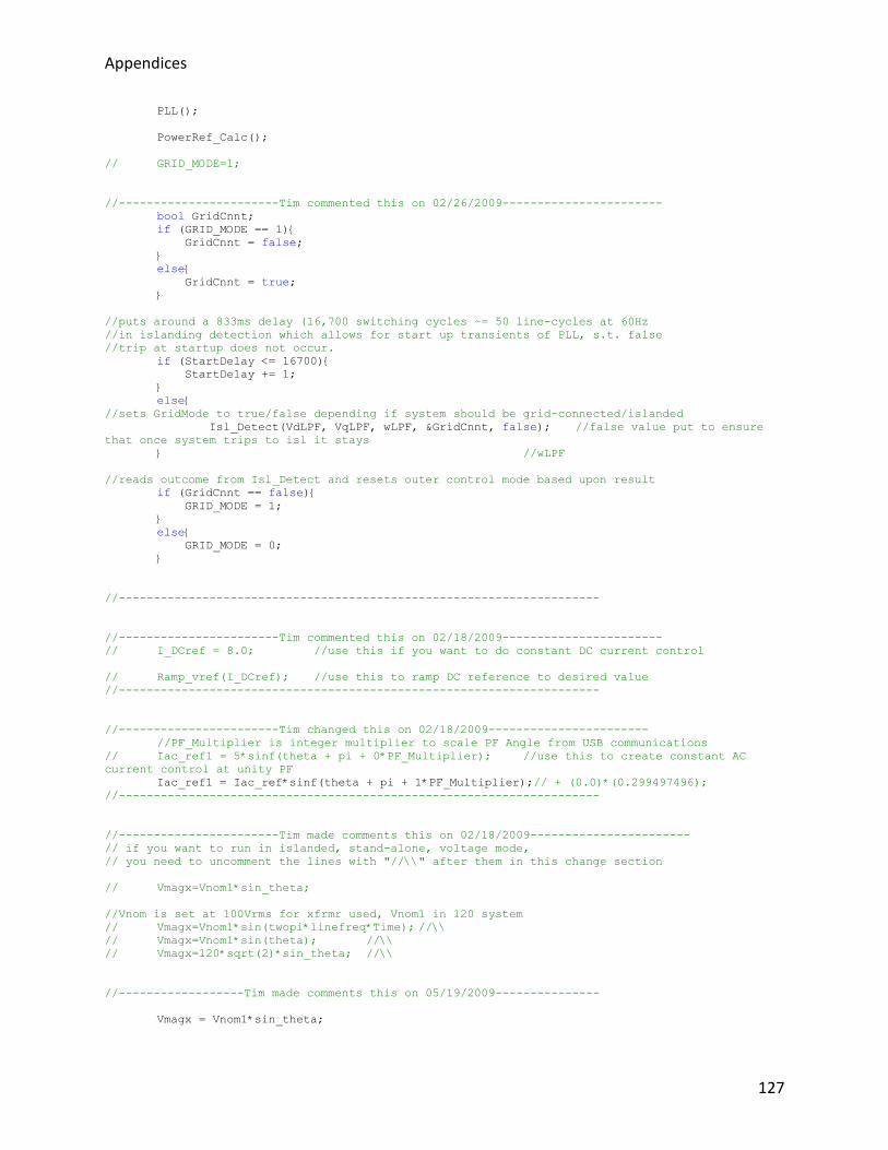
Appendices
127
PLL();
PowerRef_Calc();
// GRID_MODE=1;
//-----------------------Tim commented this on 02/26/2009-----------------------
bool GridCnnt;
if (GRID_MODE == 1){
GridCnnt = false;
}
else{
GridCnnt = true;
}
//puts around a 833ms delay (16,700 switching cycles ~= 50 line-cycles at 60Hz
//in islanding detection which allows for start up transients of PLL, s.t. false
//trip at startup does not occur.
if (StartDelay <= 16700){
StartDelay += 1;
}
else{
//sets GridMode to true/false depending if system should be grid-connected/islanded
Isl_Detect(VdLPF, VqLPF, wLPF, &GridCnnt, false); //false value put to ensure
that once system trips to isl it stays
} //wLPF
//reads outcome from Isl_Detect and resets outer control mode based upon result
if (GridCnnt == false){
GRID_MODE = 1;
}
else{
GRID_MODE = 0;
}
//---------------------------------------------------------------------
//-----------------------Tim commented this on 02/18/2009-----------------------
// I_DCref = 8.0; //use this if you want to do constant DC current control
// Ramp_vref(I_DCref); //use this to ramp DC reference to desired value
//---------------------------------------------------------------------
//-----------------------Tim changed this on 02/18/2009-----------------------
//PF_Multiplier is integer multiplier to scale PF Angle from USB communications
// Iac_ref1 = 5*sinf(theta + pi + 0*PF_Multiplier); //use this to create constant AC
current control at unity PF
Iac_ref1 = Iac_ref*sinf(theta + pi + 1*PF_Multiplier);// + (0.0)*(0.299497496);
//---------------------------------------------------------------------
//-----------------------Tim made comments this on 02/18/2009-----------------------
// if you want to run in islanded, stand-alone, voltage mode,
// you need to uncomment the lines with "//\\" after them in this change section
// Vmagx=Vnom1*sin_theta;
//Vnom is set at 100Vrms for xfrmr used, Vnom1 in 120 system
// Vmagx=Vnom1*sin(twopi*linefreq*Time); //\\
// Vmagx=Vnom1*sin(theta); //\\
// Vmagx=120*sqrt(2)*sin_theta; //\\
//------------------Tim made comments this on 05/19/2009---------------
Vmagx = Vnom1*sin_theta;
Appendices
128
if (GRID_MODE == 0){
Vmagx = Vac;
// yv_inv[0] = Iac_ref1;
}
// Vac_err = Vmagx - Vac;
// Vac_Comp();
//added on 05/20/2009 to ramp voltage reference for SAM from Vac to Vmagx
//smooths voltage reference s.t. there is not an abrupt change in Vref for SAM
Ramp_Ref(&Vmagy, Vmagx, 5);
if (GRID_MODE == 1){
Vac_err = Vmagy - Vac;
Vac_Comp();
Iac_ref1 = Iac_refx;
}
//---------------------------------------------------------------------
//----------------------Tim added this on 02/25/2009----------------------------------
//if system is in grid-connected mode, then the outer voltage loop should just track Power loop
output
/*
if (GRID_MODE == 0){
Vmagx = Vac; //forces Vac_err = 0;
// yv_inv[0] = Iac_ref1; //forces outer voltage loop in Vac_Comp() to track grid-
connected loop
// Iac_refx = Iac_ref1;
}
*/
/*
Vac_err=Vmagx-Vac; //\\
// GRID_MODE=1; //\\
Vac_Comp(); //\\
*/
// Vac_err=Vmag-Charge_I;
//---------------------------------------------------------------------
/*
//-----------------------Tim added this on 02/25/2009-----------------------
//if islanding detection determines
if (GRID_MODE == 1){
Vac_err = Vmagx - Vac;
Vac_Comp();
//Vdc_PI_Comp();
Iac_ref1 = Iac_refx;
}
//---------------------------------------------------------------------
*/
//-----------------------Tim added this on 02/18/2009-----------------------
Iac_err=Iac_ref1 - Iac; // calculate Iac error //use this for the grid-
connected mode of operation, Iac_ref1 is above, and Iac_ref from calc from P,Q demands
// Iac_err=Iac_refx - Iac; // calculate Iac error //use this for the stand-
alone mode of operation, Iac_refx comes from Vdc_PI_Comp() function
//---------------------------------------------------------------------
// Test_DAC = !Test_DAC;
// float freq_pll = w / twopi;
// unsigned int nDACA = (0.4*sin(twopi*linefreq*Time) + 0.5)*bitDAC;
unsigned int nDACA = 0.8*GRID_MODE*bitDAC;
// unsigned int nDACA = 0.95*((freq_pll - 60.0)/10.0 + 0.5)*bitDAC;
*g_cpwDACCHA = nDACA;
// unsigned int nDACB = 0.8*(0.5*Vmagy/Vnom1 + 0.5)*bitDAC;
Appendices
129
// *g_cpwDACCHB = nDACB;
unsigned int nDACB = 0.8*GRID_MODE*bitDAC;
*g_cpwDACCHB = nDACB;
/*
unsigned int nDACA = (0.5*(Vac/Vpk)+0.5)*bitPer;
*g_cpwDACCHA = nDACA;
unsigned int nDACB = (0.5*(Vmagx/Vpk)+0.5)*bitPer;
*g_cpwDACCHB = nDACB;
*/
// *g_cpwDACCHA = (UINT*) (0.5*(Vac/Vpk)+0.5)*bitPer;
// *g_cpwDACCHB = (UINT*) (0.5*(Vmagx/Vpk)+0.5)*bitPer;
Iac_PI_Comp();
De_sat(); //saturation
Power_Calc();
if (Dump_Mem == 1){
if (index2 < 1000){
Iac_check[index2] = Iac;
Iref_check[index2] = Iac_ref1;
Vdc_check[index2] = Vdc;
Vac_check[index2] = Vac;
Vacg_check[index2] = Vac_grid;
w_check[index2] = wLPF;
index2 += 1;
}
/* else{
index2 = 0;
Iac_check[index2] = Iac;
Iref_check[index2] = Iac_ref;
Vdc_check[index2] = Vdc;
Vac_check[index2] = Vac;
Vacg_check[index2] = Vac_grid;
index2 += 1;
}*/
}
/*
if (index>1000){
index = 0;
}
Vac_check[index]=Vac;
Vmag_check[index]=Vmagx;
theta_check[index]=theta;
DAC_check[index]=nDACA;
Vd_check[index]=VdLPF;
Vq_check[index]=VqLPF;
Id_check[index]=IdLPF;
Iq_check[index]=IqLPF;
Sg_check[index]=S_g;
Pg_check[index]=ACTIVE_POWER;
Qg_check[index]=REACTIVE_POWER;
index+=1;
*/
}

Appendices
130
Resynchronization and Reclosure Code
#include <sysreg.h>
#include <def21160.h>
#include <math.h>
#include <signal.h>
#include <stdio.h>
#include <stdlib.h>
#include <21160.h>
#include "UControl.h"
#include "Parameters.h"
#include "functions.h"
void Ramp_vref(float);
void Input_filter(void);
void Vdc_PI_Comp(void);
void Iac_PI_Comp(void);
void De_sat(void);
void Ramp_iref(void);
//void maindd(void){while(1){}};
//Parameter array that interacts with USB
extern int g_nParamArray[15];
//////////////////////////////////////////////////////////////////////////////////
// <SUMMARY>Write a value to the hex display. </SUMMARY>
inline void HexWrite( const unsigned int nVal ){
*(volatile UINT*)(0x0A000000) = nVal;
}
UINT g_nCurrPkt1Prev;
UINT g_nNextActivation;
/// <SUMMARY>Read data from FPGA memory</SUMMARY>
/// <REMARKS>This function is used to read data from the FPGA and includes the timing
/// delay necessary to prevent deadlock.</REMARKS>
/// <PARAM name="nAddr">This is the address of the FPGA memory location to read.</PARAM>
//#pragma pure
unsigned int FPGARead( const unsigned int nAddr ){
asm("nop;");
volatile unsigned int* pInt = (unsigned int*)(nAddr);
unsigned int nRet = 0;
nRet = *pInt;
asm("nop;");
return nRet;
}
/// <SUMMARY>Write data to the FPGA</SUMMARY>
/// <PARAM name="nAddr">Target address to write to.</PARAM>
/// <PARAM name="nVal">Value to write to the address</PARAM>
void FPGAWrite( const unsigned int nAddr, const unsigned int nVal ){
asm("nop;");
volatile unsigned int* pInt = (unsigned int*)(nAddr);
*pInt = nVal;
asm("nop;");
}
/// <SUMMARY>Delay process used to wait in the DSP.</SUMMARY>
/// <PARAM name="nMaxCtr">This is a counter that indicates how many wait loops should
execute.</PARAM>
#pragma const
void DelayProc(const unsigned int nMaxCtr){
unsigned int n;
for( n = 0; n < nMaxCtr; n++ ){
asm("nop;");
asm("nop;");
asm("nop;");
}
}

Appendices
131
//////////////////////////////////////////////////////////////////////////////////
/// <SUMMARY>Write to USB device and do not assert ackstat. </SUMMARY>
void USBWrite( const UINT nReg, const UINT nValue, const UINT nMarker ){
UINT nOutVal = nMarker & 0xFFFF0000;
UINT nCmd = ((nReg << 3))&0xF8; //mask address
nCmd = nCmd | 0x02; //write
nOutVal = nOutVal | (nCmd << 8 );
nOutVal = nOutVal | (nValue & 0xFF );
FPGAWrite( 0x14000000, nOutVal );
}
//////////////////////////////////////////////////////////////////////////////////
/// <SUMMARY>Write to USB device and assert ackstat. </SUMMARY>
void USBWriteAS( const UINT nReg, const UINT nValue, const UINT nMarker ){
UINT nOutVal = nMarker & 0xFFFF0000;
UINT nCmd = ((nReg << 3))&0xF8; //mask address
nCmd = nCmd | 0x02; //write
nCmd = nCmd | 0x01; //Enable ACKSTAT
nOutVal = nOutVal | (nCmd << 8 );
nOutVal = nOutVal | (nValue & 0xFF );
FPGAWrite( 0x14000000, nOutVal );
}
//////////////////////////////////////////////////////////////////////////////////
/// <SUMMARY>Read USB register and do not set acknowledge bit.</SUMMARY>
void USBRead( const UINT nReg, const UINT nMarker ){
UINT nOutVal = nMarker & 0xFFFF0000;
const UINT nCmd = ((nReg << 3)&0xF8); //mask address
nOutVal = nOutVal | (nCmd << 8 );
FPGAWrite( 0x14000000, nOutVal );
}
//////////////////////////////////////////////////////////////////////////////////
/// <SUMMARY>Read USB register and set acknowledge bit.</SUMMARY>
void USBReadAS( const UINT nReg, const UINT nMarker ){
UINT nOutVal = nMarker & 0xFFFF0000;
UINT nCmd = ((nReg << 3)&0xF8); //mask address
nCmd = nCmd | 0x01; //Enable ACKSTAT
nOutVal = nOutVal | (nCmd << 8 );
FPGAWrite( 0x14000000, nOutVal );
}
void mainUSB(void);
void UpdateUSBParameters(){
g_nParamArray[0]=MODE_STATUS;
g_nParamArray[1]=*(int*)(&ACTIVE_POWER);
g_nParamArray[2]=*(int*)(&REACTIVE_POWER);
g_nParamArray[3]=Batt_SOC;
MODE_DEMAND=g_nParamArray[4];
//P_DEMAND=*(int*)(&g_nParamArray[5]);
//Q_DEMAND=*(int*)(&g_nParamArray[6]);
VOLTAGE=g_nParamArray[7]; //RMS Voltage
FREQ=g_nParamArray[8]; //59900, 60000, or 60100 mHz
//g_nParamArray[9] = Iac_refPQ;
sync_cmd = *(int*)(&g_nParamArray[9]);
g_nParamArray[10] = P_DEMAND;
g_nParamArray[11] = Q_DEMAND;
Dump_Mem = g_nParamArray[12];
//MODE_DEMAND=g_nParamArray[10];
//GRID_MODE = g_nParamArray[11];
//PF_Multiplier = g_nParamArray[12];

Appendices
132
//DC_Current_Command = g_nParamArray[4];
}
int main()
{
sysreg_bit_set(sysreg_MODE2, IRQ0E); //enable /IRQ0
sysreg_bit_clr(sysreg_MODE1, IRPTEN);
//////////////////////////////////////////////////////
*g_cpwDACCTL = 0x00000003; // Initialization of DAC
*g_cpwDACCTL = 0x00000002; // Initialization of DAC
*g_cpwDACCTL = 0x00000003; // Initialization of DAC
/////////////////////////////////////////////////////
ConfigurePWM(); //send out the first data
interrupt (SIG_IRQ0,irq0_handler); //Interrupt
// sysreg_bit_clr(sysreg_MODE1, IRPTEN); //enable global interrupt
while(1){
asm("nop;");
asm("nop;");
asm("nop;");
//USB Main function
mainUSB();
//maindd();
}
}
void ConfigurePWM()
{
*g_cpwPer = bitPer; // Switching Period expressed in clock cycles Tsw/
12.5ns
*g_cpwDeadtime = 100; // Deadtime expressed in clock cycles 1us/
12.5ns
*g_cpwPD = 100; // Pulse Deletion expressed in clock cycles 0/ 12.5ns
*g_cpwDuty = 0.2*bitPer;
*g_cpwMod_SEL = 1; // when 1 Unipolar, When 0 Bipolar
*g_cpwCurr_Dir = 0; // Current Direction used for deadtime compensation
*reset_ff = 1; // reset D flipflop
*reset_ff2 = 1; // reset D flipflop
*reset_ff3 = 1; // reset D flipflop
*relay = 1; // reset relay
// *HSFan = 0; // reset HSFan
*g_cpwDeadCom = DTC_OnOff; //reset deadtime compensation
}
///////////////////////////////////////////////////////////////////
//AD data read out
void ADScale()
{
float IL_Temp;
float Vdc_Temp;
float Vac_Temp;
float Vacg_Temp;
float HS_Temp;
int ADC_CHA= *reg_ADC2CHA;
int ADC_CHB= *reg_ADC1CHB;
int ADC_CHC= *reg_ADC2CHC;
int ADC_CHD= *reg_ADC1CHA;
//converting 2's compliments to float
//-------------------------------
if(ADC_CHA >= 0x800)
IL_Temp = (-(~(ADC_CHA-1) & 0xfff)+CHC1_CHA_OFFSET)/CHC1_CHA_SCALE;
else

Appendices
133
IL_Temp = (ADC_CHA+CHC1_CHA_OFFSET)/CHC1_CHA_SCALE;
//-------------------------------
//-------------------------------
if(ADC_CHB >= 0x800)
Vac_Temp = (-(~(ADC_CHB-1) & 0xfff)+CHC1_CHB_OFFSET)/CHC1_CHB_SCALE;
else
Vac_Temp = (ADC_CHB+CHC1_CHB_OFFSET)/CHC1_CHB_SCALE;
//-------------------------------
//-------------------------------
if(ADC_CHC >= 0x800)
Vdc_Temp = (-(~(ADC_CHC-1) & 0xfff)+CHC2_CHA_OFFSET)/CHC2_CHA_SCALE;
else
Vdc_Temp = (ADC_CHC+CHC2_CHA_OFFSET)/CHC2_CHA_SCALE;
//-------------------------------
/*
//-------------------------------
if(ADC_CHD >= 0x800)
Charge_I = (-(~(ADC_CHD-1) & 0xfff)+CHC2_CHB_OFFSET)/CHC2_CHB_SCALE;
else
Charge_I = (ADC_CHD+CHC2_CHB_OFFSET)/CHC2_CHB_SCALE;
//-------------------------------
*/
//-------------------------------
if(ADC_CHD >= 0x800)
Vacg_Temp = (-(~(ADC_CHD-1) & 0xfff)+CHC2_CHB_OFFSET)/CHC2_CHB_SCALE;
else
Vacg_Temp = (ADC_CHD+CHC2_CHB_OFFSET)/CHC2_CHB_SCALE;
//-------------------------------
Iac = ( IL_Temp - 0.152463 ) * 21.2;// - 0.299497496;
// Setting the polarity right
Vac = ( Vac_Temp + 0.009 ) * 22.9 *(1.0);
Vac_grid = ( Vacg_Temp + 0.009 ) * 22.9 *(1.0);
Vdc = ( Vdc_Temp + 8.0235 ) * 27.205;
// Charge_I = Charge_I * (1000/328.0);
}
/////////////////////////////////////////////////////////////////////////////////////////////////
///////////////////
//interrupt routine
void irq0_handler(int useless)
{
while(*reg_ADAV==0)
asm("nop;");
//////////////////
ADScale();
//////////////////
// Protection();
//////////////////
///////////////////////////////////////////////////////////
Open_Close_Sel=0;
if (Open_Close_Sel==1)
Openloop(); //openloop control
else if (Open_Close_Sel==0)
{
Closedloop(); //closedloop control
Duty = (bitPer * 0.5) + (bitPer * 0.5) * Duty_ab; //transfer to counter number
// Duty=0;
}
////////////////////////////////////////////////////////////
if(Iac>0) //determine current direction

Appendices
134
Curr_Dir=1;
else if(Iac<=0);
Curr_Dir=0;
SwPer=bitPer; //12.5ns * #
DeadTime=160;
PD=100;
Mod_Sel=1;
///////////////////
Update();
//////////////////////////////////////
Time+=TimeInc;
if(Time>100/linefreq) {Time-=100/linefreq; counter_check++;}
/////////////////////////////////////////////////
if(counter_check>2)
{
counter_check=3;
if(index<1000)
{w_check[index]=Duty_ab;
index++;}
}
////////////////////////////////////////////////
}
/////////////////////////////////////////////////////////////////////////////////////////////////
//////////////////
//openloop test
float fMag = 0.85;
unsigned int nDutyOverride = 3738;
bool bEven = false;
void Openloop()
{
//```````````````````````````````````````````````
if(InitTime>5e-3) // wait for 5ms
if(Mod_indexopen<0.7)
Mod_indexopen+=0.01; //increase Modindex
else
{Mod_indexopen=0.7;
InitTime=6e-3;}
else if(InitTime<=5e-3)
InitTime+=TimeInc;
//````````````````````````````````````````````````
Duty = (bitPer * 0.5) +(bitPer * 0.5) * (sinf(2*pi*linefreq*Time) * 0.7);//Mod_indexopen);
// Duty = 0;
// DeadTime=(bitPer * 0.5) +(bitPer * 0.5) * (sinf(2*pi*linefreq*Time) * 0.7);
//````````````````````````````````````````````````
*g_cpwDACCHA=Duty;//15*(Vac+150); //DAC check
*g_cpwDACCHB=Duty;
//```````````````````````````````````````````````
SwPer=bitPer; //12.5ns * #
// bEven = !bEven;
DeadTime=160;//( bEven? 160:170);
PD=100;
Mod_Sel=1; //0=bipolar, 1=unipolar
Curr_Dir=0;
//````````````````````````````````````````````````
}
////////////////////////////////////////////////////////////////////////////////////////////
//Update Value
void Update()

Appendices
135
{
*g_cpwDuty = Duty; //Reference waveform
*g_cpwPer = SwPer; //Switching period
*g_cpwDeadtime = DeadTime; //Deadtime
*g_cpwPD = PD; //Pulse Deletion
*g_cpwMod_SEL = Mod_Sel;
*g_cpwCurr_Dir = Curr_Dir;
// *reset_ff = 1;
// *reset_ff2 = ff_state;
// *reset_ff3 = ff_state;
//*HSFan = 0;
*g_cpwDeadCom = DTC_OnOff;
}
////////////////////////////////////////////////////////////////////////////////////////
// Protection Block
void Protection()
{
if(abs(Iac)>=150 || Vdc>=380 )
*relay=0; // relay_control
else if(abs(Iac)<=130 && Vdc<=350 )
*relay=1;
else if((abs(Iac)>130 && abs(Iac)<150) || (Vdc>350 && Vdc<380) )
*relay=old_relay;
else
*relay=1;
old_relay=*relay; //histersis
if(*relay==0) fault=1;
if(*relay==1 && fault==1) count++;
if(*relay==0 && count>0) count=0;
while(*relay==1 && count>=50 )
{
ff_state=0;
fault=0;
count=0;
clear=1;
}
for(;clear==1;count++)
while(clear==1 && count>=3)
{
ff_state=1;
count=0;
clear=0;
}
}
////////////////////////////////////////////////
//Input_filter for sensored signal
void Input_filter() //
{
// Vdc_filter = LPF_a1*Vdc_I[0]+LPF_a2*Vdc_I[1];
// Vac_filter = LPF_a1*Vac_I[0]+LPF_a2*Vac_I[1];
Iac_filter = LPF_a1*Iac_I[0]+LPF_a2*Iac_I[1];
// Vdc_I[0]=Vdc_I[1];
// Vdc_I[1]=Vdc;
// Vac_I[0]=Vac_I[1];
// Vac_I[1]=Vac;
Iac_I[0]=Iac_I[1];
Iac_I[1]=Iac;
}

Appendices
136
////////////////////////////////////////////////////
void Ramp_vref(float Vlimit)
{
if(Vmag < Vlimit-0.02)
Vmag += 0.01;
else if(Vmag > Vlimit+0.02)
Vmag -= 0.01;
else
Vmag = Vlimit;
}
//////////////////////////////////////////////////
/*
void Ramp_Ref(float* pMagRef, float pMagCmd)
{
//if new reference (minus 0.02) is < present reference increase by 0.01 until condition
met
if( *pMagRef < (pMagCmd - 0.02) ){
*pMagRef += 0.01;
}
//else if new reference (minus 0.02) is > present reference decrease by 0.01 until
condition met
else if ( pMagCmd < (*pMagRef + 0.02) ){
*pMagRef -= 0.01;
}
//otherwise, ramped reference has reached commanded reference so set reference to
commanded reference
else{
*pMagRef = pMagCmd;
}
}
*/
///////////////////////////////////////////////////
//////////////////////////////////////////////////
void Ramp_Ref(float* pMagRef, float pMagCmd, float RampStep)
{
//if ref command (minus 0.02) is > present ref, increase by 0.01 until condition met
if( *pMagRef < (pMagCmd - 2*RampStep) ){
*pMagRef += RampStep;
}
//else if ref command (plus 0.02) is < present ref, decrease by 0.01 until condition met
else if ( *pMagRef > (pMagCmd + 2*RampStep) ){
*pMagRef -= RampStep;
}
//otherwise, ramped reference has reached commanded reference so set reference to
commanded reference
else{
*pMagRef = pMagCmd;
}
}
///////////////////////////////////////////////////
///////////////////////////////////////////////////
void Isl_Detect(const float pVd, const float pVq, const float w_PLL, bool* pGridOk, bool
Remote_GridOk)
{
const float Vdq = sqrt(pVd*pVd + pVq*pVq);
const float f_line = w_PLL / twopi;
if ( *pGridOk == true ){

Appendices
137
if ( (Vdq >= 0.88*Vnom1) && (Vdq <= 1.1*Vnom1) && (f_line >= flimit_lower) && (f_line <=
flimit_higher) ){
*pGridOk = true;
}
else{
*pGridOk = false;
}
}
else{
if (Remote_GridOk == true){
*pGridOk = true;
}
else{
*pGridOk = false;
}
}
}
///////////////////////////////////////////////////
///////////////////////////////////////////////////
void DQ_TransformV(const float Va, const float w_PLLv, float* pVd, float* pVq)
{
float dVy, dVz;
Valpha = Va;
dVz = w_PLLv*Valpha;
dVy = (Vz - Valpha - Vy)*w_PLLv;
Vz = Vz + Period*dVz;
Vy = Vy + Period*dVy;
Vbeta = Vz - Valpha - Vy;
//DQ (Park's) Transform
*pVd = Valpha*sin_theta - Vbeta*cos_theta;// + 0.8;
*pVq = Valpha*cos_theta + Vbeta*sin_theta;// + 2.5;
}
///////////////////////////////////////////////////
///////////////////////////////////////////////////
void DQ_TransformI(const float Ia, const float w_PLLi, float* pId, float* pIq)
{
float dIy, dIz;
Ialpha = Ia;
dIz = w_PLLi*Ialpha;
dIy = (Iz - Ialpha - Iy)*w_PLLi;
Iz = Iz + Period*dIz;
Iy = Iy + Period*dIy;
Ibeta = Iz - Ialpha - Iy;
//DQ (Park's) Transform
*pId = Ialpha*sin_theta - Ibeta*cos_theta;
*pIq = Ialpha*cos_theta + Ibeta*sin_theta;
}
///////////////////////////////////////////////////
void Ramp_iref()
{
if(Imag < 1.98)
Imag += 0.001;
else
Imag = 2.0;
}
///////////////////////////////////////////////////

Appendices
138
void Vac_PI_Comp()
{
yv_inv[2]=yv_inv[1];
yv_inv[1]=yv_inv[0];
xv_inv[2]=xv_inv[1];
xv_inv[1]=xv_inv[0];
xv_inv[0]=Vac_err;
yv_inv[0]=0.1*(xv_inv[0]+0.1799*xv_inv[1]-0.8201*xv_inv[2])+1.2953*yv_inv[1]-
0.2953*yv_inv[2];
yv[0] = yv_inv[0];
if(yv[0]>=30)
yv[0]=30;
if(yv[0]<=-30)
yv[0]=-30;
Iac_ref=yv[0];
}
///////////////////////////////////////////////////
void Vdc_PI_Comp()
{
if (GRID_MODE == 0){
////*********************current charge/discharge controller****************
yv_iDC[3]=yv_iDC[2];
yv_iDC[1]=yv_iDC[0];
yv_iDC[2]=1.4721/2*Vac_err+yv_iDC[3];
yv_iDC[0]=yv_iDC[2]*50e-6+(1-96.3*50e-6)*yv_iDC[1];
yv[0] = yv_iDC[0];
////************************************************************
}
else if (GRID_MODE == 1){
////**********************AC voltage inverter test*************************
yv_inv[2]=yv_inv[1];
yv_inv[1]=yv_inv[0];
xv_inv[2]=xv_inv[1];
xv_inv[1]=xv_inv[0];
xv_inv[0]=Vac_err;
yv_inv[0]=0.1*(xv_inv[0]+0.1799*xv_inv[1]-0.8201*xv_inv[2])+1.2953*yv_inv[1]-
0.2953*yv_inv[2];
yv[0] = yv_inv[0];
// Int_Vac_PLL_d = Int_Vac_PLL + 20*Vac_err*Period;
// Pro_Vac_PLL_d = 0.2*Vac_err;
// yv[0] = (Int_Vac_PLL_d + Pro_Vac_PLL_d);
////************************************************************
}
else if (GRID_MODE == 2){
////***********************************DC voltage rectifier test***************
yv_rec[3]=yv_rec[2];
yv_rec[1]=yv_rec[0];
xv_rec[1]=xv_rec[0];
xv_rec[0]=Vac_err;
yv_rec[2]=xv_rec[0]+(13.7*50e-6-1)*xv_rec[1]-(30.5*50e-6-1)*yv_rec[3];
yv_rec[0]=20*50e-6*yv_rec[2]+yv_rec[1];
yv[0] = yv_rec[0];
////**************************************************************
}
else if (GRID_MODE == 3) { //singe-phase dq
Int_Vac_PLL_d = Int_Vac_PLL_d + 300*Vac_err_d*Period;
Pro_Vac_PLL_d = 0.4*Vac_err_d;
Int_Vac_PLL_q = Int_Vac_PLL_q + 300*Vac_err_q*Period;

Appendices
139
Pro_Vac_PLL_q = 0.4*Vac_err_q;
yv[0] = cos(twopi*linefreq*Time)*(Int_Vac_PLL_d +
Pro_Vac_PLL_d)+sin(twopi*linefreq*Time)*(Int_Vac_PLL_q + Pro_Vac_PLL_q);
}
////**************************************************************
else if (GRID_MODE == 4) { //PR
yv_inv[2]=yv_inv[1];
yv_inv[1]=yv_inv[0];
xv_inv[2]=xv_inv[1];
xv_inv[1]=xv_inv[0];
xv_inv[0]=Vac_err;
// yv_inv[0]=0.6*Vac_err-1.14*xv_inv[1]+0.54*xv_inv[2]+2*yv_inv[1]-1*yv_inv[2];
yv_inv[0]=0.57*Vac_err-1*xv_inv[1]+0.43*xv_inv[2]+2*yv_inv[1]-1*yv_inv[2];
yv[0] = yv_inv[0];
}
else{
yv[0] = 0;
}
if(yv[0]>=30)
yv[0]=30;
if(yv[0]<=-30)
yv[0]=-30;
Iac_ref=yv[0];
}
/*
////////////////////////////////////////////////////
void PLL()
{
//index_PLL, 334 = one-line cycle @ 60Hz
if ((MODE_DEMAND == 0x0fffffff) && (index_PLL >= 6680) ){
Err_PLL = (Vac/Vnom1)*cos_theta - sin_theta*cos_theta;
//Vnom = 100 Vrms
//Vnom1 = 120 Vrms
Int_Vac_PLL = Int_Vac_PLL + Ki_PLL*Err_PLL*Period;
Pro_Vac_PLL = Kp_PLL*Err_PLL;
w = Int_Vac_PLL + Pro_Vac_PLL + twopi*f_line;
}
else{
w = twopi*linefreq;
if (MODE_DEMAND == 0x0fffffff){
index_PLL += 1;
}
}
// equivalent if/else statements for upper and lower frequency limits on PLL
w = ( (w <= twopi*flimit_hPLL) ? w : (twopi*flimit_hPLL) );
w = ( (w >= twopi*flimit_lPLL) ? w : (twopi*flimit_lPLL) );
theta = theta + w*Period;
if (theta > twopi){
theta -= twopi;
}
else if (theta < 0.0){
theta += twopi;
}

Appendices
140
cos_theta = cosf(theta);
sin_theta = sinf(theta);
}
////////////////////////////////////////////////////
*/
////////////////////////////////////////////////////
void PLL_sync()
{
if (sync_cmd == 1){
//Err_PLL = (Vac/Vnom1)*cos_theta - sin_theta*cos_theta;
//Vnom = 100 Vrms
//Vnom1 = 120 Vrms
// Err_PLL = theta_g - theta;
Err_PLL = sin_theta_g*cos_theta - sin_theta*cos_theta;
Int_Vac_PLL = Int_Vac_PLL + Ki_PLL*Err_PLL*Period;
Pro_Vac_PLL = Kp_PLL*Err_PLL;
w = Int_Vac_PLL + Pro_Vac_PLL + twopi*f_line;
// w = Int_Vac_PLL + Pro_Vac_PLL + w_g;
}
else{
w = twopi*f_line;
}
// equivalent if/else statements for upper and lower frequency limits on PLL
w = ( (w <= twopi*flimit_hPLL) ? w : (twopi*flimit_hPLL) );
w = ( (w >= twopi*flimit_lPLL) ? w : (twopi*flimit_lPLL) );
theta = theta + w*Period;
if (theta > twopi){
theta -= twopi;
}
else if (theta < 0.0){
theta += twopi;
}
cos_theta = cosf(theta);
sin_theta = sinf(theta);
}
////////////////////////////////////////////////////
////////////////////////////////////////////////////
void PLL_grid()
{
Err_PLL_g = (Vac_grid/Vnom1)*cos_theta_g - sin_theta_g*cos_theta_g;
//Vnom = 100 Vrms
//Vnom1 = 120 Vrms
Int_Vac_PLL_g = Int_Vac_PLL_g + Ki_PLL_g*Err_PLL_g*Period;
Pro_Vac_PLL_g = Kp_PLL_g*Err_PLL_g;
w_g = Int_Vac_PLL_g + Pro_Vac_PLL_g + twopi*f_line;
// equivalent if/else statements for upper and lower frequency limits on PLL
w_g = ( (w_g <= twopi*flimit_hPLL) ? w_g : (twopi*flimit_hPLL) );
w_g = ( (w_g >= twopi*flimit_lPLL) ? w_g : (twopi*flimit_lPLL) );
theta_g = theta_g + w_g*Period;
if (theta_g > twopi){
theta_g -= twopi;
}
else if (theta_g < 0.0){

Appendices
141
theta_g += twopi;
}
cos_theta_g = cosf(theta_g);
sin_theta_g = sinf(theta_g);
}
////////////////////////////////////////////////////
/*
////////////////////////////////////////////////////
void PLL1()
{
Err_PLL = (Vac1/Vnom1)*cos_theta - sin_theta*cos_theta;
Int_Vac_PLL = Int_Vac_PLL + Ki_PLL*Err_PLL*Period;
Pro_Vac_PLL = Kp_PLL*Err_PLL;
w = Int_Vac_PLL + Pro_Vac_PLL + twopi*linefreq;
theta = theta + w*Period;
if (theta > twopi){
theta -= twopi;
}
else if (theta < 0.0){
theta += twopi;
}
cos_theta = cosf(theta);
sin_theta = sinf(theta);
}
////////////////////////////////////////////////////
*/
////////////////////////////////////////////////////
void Iac_PI_Comp()
{
yc[3]=yc[2];
yc[2]=yc[1];
yc[1]=yc[0];
xc[3]=xc[2];
xc[2]=xc[1];
xc[1]=xc[0];
xc[0]=Iac_err;
if(Vdc>280)
KK=5*Vdc/440;
else if(Vdc<280)
KK=5;
yc[0]=0.019842*KK*(xc[0]-0.1432*xc[1]-0.824845*xc[2]+0.3183543*xc[3])-
0.5427*yc[1]+0.9599*yc[2]+0.5828*yc[3];
//yc[0]=0.019*(xc[0]-0.1344*xc[1]-0.8204*xc[2]+0.314*xc[3])-
0.5408*yc[1]+0.9592*yc[2]+0.5816*yc[3];
//0.019842 full load
//0.019 30Ohms load
if(yc[0]>=1)
yc[0]=1;
if(yc[0]<=-1)
yc[0]=-1;
Duty_ab=yc[0];

Appendices
142
////////////////////////////////////////////////////////
/*
y=(Current_I*Iac_err+K_anti*(yu_s-yy[0]))*Period;
yu=Current_P*(Iac_err-Iac_err_I[0]);
yy[1]=y+yu+yy[0];
if(abs(yy[1])<=1) yu_s=yy[1];
else if(yy[1]>1) yu_s=1;
else if(yy[1]<-1) yu_s=-1;
yy[0]=yy[1];
Iac_err_I[0]=Iac_err; //update
Duty_ab=yy[1];
*/
////////////////////////////////////////
/*
y_delta=Current_I*Iac_err*Period;
y+=y_delta;
yu=Current_P*Iac_err;
yy=y+yu;
if ( yy > 1 )
{
yy = 1;
y -= 1*y_delta; //Stop integral when saturation
}
else if ( yy < -1 )
{
yy = -1;
y -= 1*y_delta; //Stop integral when saturation
}
Duty_ab=yy;
*/
///////////////////////////////////////////
/*
Iac_err_I[0]=Iac_err_I[1]; //update
Iac_err_I[1]=Iac_err;
Dab[1]=(a1 * Iac_err_I[1]) + (a2 * Iac_err_I[0]) + Dab[0]; //PI
Dab[0]=Dab[1]; //update
//Iac_err_I[0]=Iac_err_I[1]; //update
//Iac_err_I[1]=Iac_err;
float fscale = fabs(Dab[1]);
if(fscale >= 0.9){
float fscaleinv = 1.0/fscale;
Dab[1] *= fscaleinv;
Dab[0] *= fscaleinv;
}
Duty_ab=Dab[1];
*/
///////////////////////////////////////////
}
///////////////////////////////////////////////////
////////////////////////////////////////////////////
//saturation limit for Duty cycle
void De_sat()
{
if (Duty_ab>=1)
Duty_ab=1;
else if (Duty_ab<=-1)
Duty_ab=-1;

Appendices
143
// Duty_ab = DutyHPF_C*DutyHPF_X + DutyHPF_D*Duty_ab;
// DutyHPF_X = DutyHPF_A*DutyHPF_X + DutyHPF_B*Duty_ab;
}
///////////////////////////////////////////////////
///////////////////////////////////////////////////
void ChargeCurrentRef()
{
if (Vdc <= 306.0){
I_DCref = 6.0;
Charge_flag=0;
}
else if ((Vdc <= 308.0) && Charge_flag==0 && StopCharge_flag==0){
I_DCref = 6.0;
}
else if (Vdc <= 312.2 && Charge_flag1==0 && StopCharge_flag==0){
Charge_flag=1;
I_DCref = 3.0;
Charge_flag1=0;
}
else if ((Vdc <= 314.2) && Charge_flag1==0 && StopCharge_flag==0){
I_DCref = 3.0;
}
else if (Vdc <= 322.2 && Charge_flag2==0 && StopCharge_flag==0){
Charge_flag1=1;
I_DCref = 2.5;
Charge_flag2=0;
}
else if ((Vdc <= 316.0) && Charge_flag2==0 && StopCharge_flag==0){
I_DCref = 2.5;
}
else if (Vdc <= 317.0){
Charge_flag2=1;
I_DCref = 1.0;
Charge_flag3=0;
}
else if ((Vdc <= 326.0) && Charge_flag3==0 && StopCharge_flag==0){
I_DCref = 1.0;
}
else if (Vdc <= 327.0 && StopCharge_flag==0){
Charge_flag3=1;
I_DCref = 0.3;
StopCharge_flag=0;
}
else if ((Vdc < 328.0) && StopCharge_flag==0){
I_DCref = 0.3;
}
else if ((Vdc <= 330.0)){
I_DCref = 0.0;
StopCharge_flag = 1;
}
else{
I_DCref = 0.0;
StopCharge_flag = 1;
}
}
///////////////////////////////////////////////////
///////////////////////////////////////////////////
void StateOfCharge()
{
// SOC 0 - 60
if (Charge_flag == 0){
Batt_SOC = (Vdc*8/14)/3.3;
}
// SOC 61 - 70
else if (Charge_flag == 1){
Batt_SOC = 65;
}

Appendices
144
// SOC 71 - 80
else if (Charge_flag1 == 1){
Batt_SOC = 75;
}
// SOC 81 - 90
else if (Charge_flag2 == 1){
Batt_SOC = 85;
}
// SOC 91 - 100
else if (Charge_flag3 == 1){
Batt_SOC = 95;
}
}
///////////////////////////////////////////////////
///////////////////////////////////////////////////
void Power_Calc()
{
DQ_TransformV(Vac, twopi*linefreq, &Vd, &Vq);
DQ_TransformI(Iac, twopi*linefreq, &Id, &Iq);
////////////////////
//LPF of Vdq & idq//
////////////////////
VdLPF = C1_LPF*X1_LPF;
X1_LPF = A1_LPF*X1_LPF + B1_LPF*(Vd+0.8);
////////////////
VqLPF = C1_LPF*X2_LPF;
X2_LPF = A1_LPF*X2_LPF + B1_LPF*(Vq+1.563);
////////////////
IdLPF = C1_LPF*X3_LPF;
X3_LPF = A1_LPF*X3_LPF + B1_LPF*Id;
////////////////
IqLPF = C1_LPF*X4_LPF;
X4_LPF = A1_LPF*X4_LPF + B1_LPF*Iq;
////////////////
wLPF = C1_LPF*Xw_LPF;
Xw_LPF = A1_LPF*Xw_LPF + B1_LPF*w;
////////////////
ACTIVE_POWER = -(VdLPF*IdLPF + VqLPF*IqLPF)/2;// VdLPF*IdLPF/2;
REACTIVE_POWER = -(VdLPF*IqLPF - VqLPF*IdLPF)/2;//VdLPF*IqLPF/2;
/* float V_pk = sqrt(VdLPF*VdLPF + VqLPF*VqLPF);
float I_pk = sqrt(IdLPF*IdLPF + IqLPF*IqLPF);
S_g = V_pk * I_pk / 2;
if (Charge_I < 0){
signP_g = -1;
}
else{
signP_g = 1;
}
*/
/*
ACTIVE_POWER = S_g * cosf(PF_Angle) * signP_g;
REACTIVE_POWER = S_g * sinf(PF_Angle);
//Q = P * tan(phi)
*/
}
///////////////////////////////////////////////////
/*
///////////////////////////////////////////////////
void PowerRef_Calc()
{

Appendices
145
// P_DEMAND = 0xffffff38;
// Q_DEMAND = 0xffffff38;
ChargeCurrentRef();
StateOfCharge();
if(P_DEMAND < 0)
{
P_DEMAND = ((~(P_DEMAND-1)));
P_d = -*(int*)(&P_DEMAND);
P_DEMAND = ((~(P_DEMAND-1)));
}
else{
P_d = *(int*)(&P_DEMAND);
}
Q_d = *(int*)(&Q_DEMAND);
S_d = sqrt(P_d*P_d + Q_d*Q_d);
if (S_d > 1.6e3){
P_d *= 1.6e3 / S_d;
Q_d *= 1.6e3 / S_d;
}
PF_Angle = atan(Q_d / P_d);
//in radians
if (MODE_DEMAND == 0x00000000)
{
MODE_STATUS=0x0000000f;
I_DCref = 0;
GRID_MODE=0;
}
else if (MODE_DEMAND == 0x01111111)//17895697)
{
MODE_STATUS=0x01111110;
I_DCref = 0;
GRID_MODE=1;
ACTIVE_POWER = 506; //
REACTIVE_POWER=30; //
}
else if (MODE_DEMAND == 0x0fffffff)//268435455 )
{
GRID_MODE=0;
MODE_STATUS=0x0ffffff0;
// ACTIVE_POWER = 106; //
//REACTIVE_POWER=90; //
I_DCref=P_d/Vdc;
if(abs(I_DCref)<=0.5)
I_DCref=0.5;
}
else if (MODE_DEMAND == 0x0bbbbbbb)//196852667)
{
MODE_STATUS=0x0bbbbbb0;
I_DCref = 0;
ACTIVE_POWER = 206; //
REACTIVE_POWER=900; //
}
else
{
MODE_STATUS=0x00000001;
// I_DCref = 0.0;
GRID_MODE=0;
ACTIVE_POWER = 6; //
REACTIVE_POWER=9; //
}
Appendices
146
}
///////////////////////////////////////////////////
*/
///////////////////////////////////////////////////
void PowerRef_Calc()
{
// P_DEMAND = 0xffffff38;
// Q_DEMAND = 0xffffff38;
//calc what Idc should be if charging
ChargeCurrentRef();
//calc batt state of charge based on Vdc
StateOfCharge();
//calc the max DC power allowed into battery
P_dcRef = Vdc*I_DCref;
//Correct the P # from hex to int, etc... if negative
if(P_DEMAND < 0)
{
P_DEMAND = ((~(P_DEMAND-1))); //Two's compliment
P_d = -*(int*)(&P_DEMAND);
P_DEMAND = ((~(P_DEMAND-1)));
}
else{
P_d = *(int*)(&P_DEMAND);
}
//reactive power demand
// Q_d = *(int*)(&Q_DEMAND) - 105;
// Q_d = *(int*)(&Q_DEMAND);
if(Q_DEMAND < 0)
{
Q_DEMAND = ((~(Q_DEMAND-1))); //Two's compliment
Q_d = -*(int*)(&Q_DEMAND);
Q_DEMAND = ((~(Q_DEMAND-1)));
}
else{
Q_d = *(int*)(&Q_DEMAND);
}
Q_d -= 105;
//gives LPF DQ voltage and current mag (= peak phase mag)
//VdLPF, VqLPF, IdLPF, IqLPF, wLPF
// LPF_DQcalc();
if (MODE_DEMAND == 0x00000000)
{
MODE_STATUS=0x0000000f;
I_DCref = 0;
Iac_refPQ=0;
GRID_MODE=0;
}
//voltage mode of operation setting
else if (MODE_DEMAND == 0x01111111)//17895697)
{
MODE_STATUS=0x01111110;
//I_DCref = 0;
//Iac_ref=0;
//GRID_MODE=1;
// ACTIVE_POWER = 506;
// REACTIVE_POWER=30;
}
//current mode of operation setting
else if (MODE_DEMAND == 0x0fffffff)//268435455 )
{

Appendices
147
// GRID_MODE=0;
MODE_STATUS=0x0ffffff0;
if (P_d > P_dcRef){
P_d = P_dcRef;
}
//calc of apparent power demand
S_d = sqrt(P_d*P_d + Q_d*Q_d);
//limit apparent power if demand is too large
if (S_d > S_limit){
//if P > Slimit then set P=Slimit and Q=0
if (P_d > S_limit){
P_d = S_limit;
Q_d = 0.0;
}
else{
//if S > Slimit, but P < Slimit, then calc new Qdemand
//Q_d = sqrt( (1.6e3)^2 - (P_d)^2 )
if (Q_DEMAND >= 0){
Q_d = sqrt(S_limit*S_limit - P_d*P_d);
}
else{
Q_d = -sqrt(S_limit*S_limit - P_d*P_d);
}
// P_d *= S_limit / S_d;
// Q_d *= S_limit / S_d;
}
}
//safety check for PF calc
if ( (P_d >= -0.1) && (P_d <= 0.1) ){
if (Q_d < -1){
PF_AngleCmd = -pi/2;
}
else if (Q_d > 1){
PF_AngleCmd = pi/2;
}
else{
PF_AngleCmd = atan2(Q_d,P_d);
}
}
else{
PF_AngleCmd = atan2(Q_d,P_d);
}
S_d = sqrt(P_d*P_d + Q_d*Q_d); //recalc S_d based on possible limited values
// Iac_ref = (2*S_d) / Vnom1;//sqrt(VdLPF*VdLPF + VqLPF*VqLPF);
//peak current reference calculation
float Iac_RefCmd = (2*S_d) / Vnom1;//sqrt(VdLPF*VdLPF + VqLPF*VqLPF);
//used to be 30
if (Iac_RefCmd > 18.0){
Iac_RefCmd = 18.0;
}
// Iac_ref = 5.0;
// Ramp_vref(Iac_ref);
Ramp_Ref(&Iac_refPQ, Iac_RefCmd, 0.001); //1mA step
Ramp_Ref(&PF_Angle, PF_AngleCmd, 0.01); //~0.57deg step
// Iac_refPQ = Iac_RefCmd;
// Vmag = Iac_ref;
/*
Appendices
148
Ramp_vref(I_DCref);
Vac_err=Vmag-Charge_I;
Vdc_PI_Comp();
*/
}
else if (MODE_DEMAND == 0x0bbbbbbb)//196852667)
{
MODE_STATUS=0x0bbbbbb0;
S_d = sqrt(P_d*P_d + Q_d*Q_d);
float Iac_RefCmd = (2*S_d) / Vnom1;//sqrt(VdLPF*VdLPF + VqLPF*VqLPF);
//used to be 30
if (Iac_RefCmd > 18.0){
Iac_RefCmd = 18.0;
}
//safety check for PF calc
if ( (P_d >= -0.1) && (P_d <= 0.1) ){
if (Q_d < -1){
PF_AngleCmd = -pi/2;
}
else if (Q_d > 1){
PF_AngleCmd = pi/2;
}
else{
PF_AngleCmd = atan2(Q_d,P_d);
}
}
else{
PF_AngleCmd = atan2(Q_d,P_d);
}
Ramp_Ref(&Iac_refPQ, Iac_RefCmd, 0.75); //750mA step
// Ramp_Ref(&PF_Angle, PF_AngleCmd, 0.5); //~28.6deg step
// PF_Angle += pi;
PF_Angle = PF_AngleCmd + 0*pi;
}
else
{
MODE_STATUS=0x00000001;
// I_DCref = 0.0;
GRID_MODE=0;
Iac_ref=0;
}
}
///////////////////////////////////////////////////
//closed loop controller
void Closedloop()
{
// used to generate Vac and Iac variables to test PLL and DQ transform
// PF_Angle = pi/3;
// Vac = 120.0*sqrt_2*sin(2*pi*linefreq*Time);
// Iac = 10.0*sqrt_2*sin(2*pi*linefreq*Time + PF_Angle);
// MODE_DEMAND = 0x0fffffff;
// Voltage1 = 120.0;
// Freq1 = 60.0;
// P_DEMAND = -2;
// Q_DEMAND = 406;
//Vac = 120.0*sqrt_2*sin(theta);
//Iac = 6.0*sqrt_2*sin(theta - 3*pi/4);
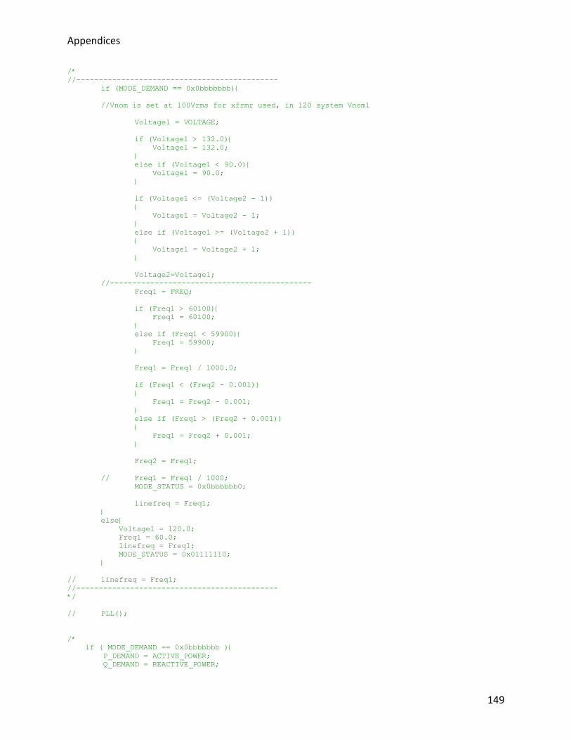
Appendices
149
/*
//---------------------------------------------
if (MODE_DEMAND == 0x0bbbbbbb){
//Vnom is set at 100Vrms for xfrmr used, in 120 system Vnom1
Voltage1 = VOLTAGE;
if (Voltage1 > 132.0){
Voltage1 = 132.0;
}
else if (Voltage1 < 90.0){
Voltage1 = 90.0;
}
if (Voltage1 <= (Voltage2 - 1))
{
Voltage1 = Voltage2 - 1;
}
else if (Voltage1 >= (Voltage2 + 1))
{
Voltage1 = Voltage2 + 1;
}
Voltage2=Voltage1;
//---------------------------------------------
Freq1 = FREQ;
if (Freq1 > 60100){
Freq1 = 60100;
}
else if (Freq1 < 59900){
Freq1 = 59900;
}
Freq1 = Freq1 / 1000.0;
if (Freq1 < (Freq2 - 0.001))
{
Freq1 = Freq2 - 0.001;
}
else if (Freq1 > (Freq2 + 0.001))
{
Freq1 = Freq2 + 0.001;
}
Freq2 = Freq1;
// Freq1 = Freq1 / 1000;
MODE_STATUS = 0x0bbbbbb0;
linefreq = Freq1;
}
else{
Voltage1 = 120.0;
Freq1 = 60.0;
linefreq = Freq1;
MODE_STATUS = 0x01111110;
}
// linefreq = Freq1;
//---------------------------------------------
*/
// PLL();
/*
if ( MODE_DEMAND == 0x0bbbbbbb ){
P_DEMAND = ACTIVE_POWER;
Q_DEMAND = REACTIVE_POWER;

Appendices
150
PowerRef_Calc();
flag_mode = 1;
}
else if (MODE_DEMAND == 0x0fffffff){
//when change into current mode from sync mode, soft-stop converter as grid
//comes online, then as
if (flag_mode == 1){
P_DEMAND = 0;
Q_DEMAND = 0;
if ( (Iac_refPQ <= 0.1) ){ // && (Iac_refPQ >= -0.1) ){
flag_mode = 0;
}
}
PowerRef_Calc();
}
*/
// PLL();
/*
float w_ac = twopi*linefreq;
theta_ac = theta_ac + w_ac*Period;
if (theta_ac > twopi){
theta_ac -= twopi;
}
else if (theta_ac < 0.0){
theta_ac += twopi;
}
sin_theta = sin(theta_ac);
cos_theta = cos(theta_ac);
*/
//---------------------------------------------
PLL_grid(); //gets grid side voltage w & theta to sync to
PLL_sync(); //generates VSC side voltage w & theta to track grid side parameters
linefreq = w / twopi;
//---------------------------------------------
// generates Vac ref from PLL values, when sync_cmd = 0, w = 2*pi*60 -> theta
// when sync_cmd = 1, w is driven to cause theta to track theta_g
Voltage1 = 120.0;
Vmag = Voltage1*sqrt(2.0)*sin_theta;
// when sync_cmd = 1 and two voltages are aligned to within 5deg and
// have less than 0.1Hz difference, system is considered synced and
// reference is set at grid side value
if (sync_cmd == 1){
// if ((abs(theta_g - theta) <= (1*pi/180)) && ((abs(w_g - w)) <= (twopi*0.1))){
// if ((abs(theta_g - theta)) <= (0.01*pi/180)){
if ( ((abs(theta_g - theta)) <= (1.0*pi/180)) && ( (abs(w_g - w)) <= (twopi*0.25)) ){
// Vmag = Vac_grid; //set Vac ref to Vgrid value
Vmag = Voltage1*sqrt(2.0)*sin_theta;
if (cntr_trackGrid <= 1000){ //3000
//track_grid = 1; //flag to confirm contorl is using Vgrid as
ref
cntr_trackGrid += 1;
}
else{
//cntr_trackGrid += cntr_trackGrid;

Appendices
151
track_grid = 1; //flag to confirm contorl is using Vgrid as
ref
Vmag = Vac_grid;
}
}
/* else{
//track_grid = 0; //keeps previously defined reference from PLL values
//cntr_trackGrid = 0;
}*/
}
else{
track_grid = 0;
cntr_trackGrid = 0;
}
// Vmag=120.0*sqrt(2.0)*sin(twopi*linefreq*Time);
// Vmag=Voltage1*sqrt(2.0)*sin(twopi*Freq1*Time);
// Vac_err=Vmag-Vdc;
Vac_err=Vmag-Vac;
Vac_PI_Comp();
//---------------------------------------------
/*
//---------------------------------------------
if (MODE_DEMAND == 0x0fffffff){
Iac_ref = Iac_refPQ*sin(theta + 1*pi + PF_Angle);// + 0.285; //0.2392578125
MODE_STATUS = 0x0ffffff0;
}
else
//---------------------------------------------
*/
//PF_Multiplier is integer multiplier to scale PF Angle from USB communications
// Iac_ref1 = 5*sinf(theta + pi + 0*PF_Multiplier);
// Iac_err=Iac_ref1-Iac; // calculate Iac error
Iac_err=Iac_ref-Iac; // calculate Iac error
Iac_PI_Comp();
De_sat(); //saturation
Power_Calc(); //calculates the P,Q values used in the system
/*
float VI_MODE = 0.0;
if (MODE_DEMAND == 0x0fffffff){
VI_MODE = 1.0;
}
else if (MODE_DEMAND == 0x0bbbbbbb){
VI_MODE = 0.25;
}
else{
VI_MODE = 0.0;
}
*/
// unsigned int nDACB = ((0.8*0.5*sin_theta) + 0.5)*bitDAC;
unsigned int nDACA = 0.8*track_grid*bitDAC;
unsigned int nDACB = 0.8*track_grid*bitDAC;
// unsigned int nDACA = 0.8*(0.5*Iac_ref/10 + 0.5)*bitDAC;
// unsigned int nDACA = 0.8*(0.5*Duty_ab + 0.5)*bitDAC;

Appendices
152
*g_cpwDACCHA = nDACA;
*g_cpwDACCHB = nDACB;
if (Dump_Mem == 1){
if (index2 < 1000){
Iac_check[index2] = Iac;
Iref_check[index2] = Iac_ref;
Vdc_check[index2] = Vdc;
Vac_check[index2] = Vac/120/sqrt_2*6;
Vacg_check[index2] = Vac_grid;
Vd_check[index2] = Vd;
Vq_check[index2] = Vq;
Id_check[index2] = Id;
Iq_check[index2] = Iq;
Valpha_check[index2] = Valpha;
Vbeta_check[index2] = Vbeta;
Ialpha_check[index2] = Ialpha;
Ibeta_check[index2] = Ibeta;
P_check[index2] = ACTIVE_POWER;
Q_check[index2] = REACTIVE_POWER;
index2 += 1;
}
/* else{
index2 = 0;
Iac_check[index2] = Iac;
Iref_check[index2] = Iac_ref;
Vdc_check[index2] = Vdc;
Vac_check[index2] = Vac;
Vacg_check[index2] = Vac_grid;
index2 += 1;
}*/
}
}

Appendices
153
USB Interface Code
#include "MAX3420E.h" // MAX3420E registers (rREGNAME), bits (bmBITNAME), and some handy
macros
#include "ENUM_APP_DATA.h" // HID keyboard enumeration data
//extern int nSelCh4;
typedef unsigned char BYTE; // these save typing
typedef unsigned short WORD;
typedef unsigned int UINT;
//////////////////////////////////////////////////
// UC Function Headers
void USBWrite( UINT nReg, UINT nValue, UINT nMarker );
void USBWriteAS( UINT nReg, UINT nValue, UINT nMarker );
void USBRead( UINT nReg, UINT nMarker );
void USBReadAS( UINT nReg, UINT nMarker );
unsigned int FPGARead( unsigned int nAddr );
void FPGAWrite( const unsigned int nAddr, const unsigned int nVal );
// void DelayProc( const UINT nTime);
void DelayProc(const unsigned int nMaxCtr);
// function prototypes
void SPI_Init(void); // Configure MAXQ2000 and MAX3420E IO pins for SPI
void Reset_MAX(void); // Reset the MAX3420E
void wreg(BYTE r,BYTE v); // Write a MAX3420E register byte
void wregAS(BYTE r,BYTE v); // Same as 'wreg' but also set the ACKSTAT bit in the SPI command
byte
BYTE rreg(BYTE r); // Read a MAX3420E register byte
BYTE rregAS(BYTE r); // Same as 'rreg' but also set the ACKSTAT bit
void readbytes(BYTE reg, BYTE N, BYTE *p); // Read N MAX3420E FIFO bytes into the array p
void writebytes(BYTE reg, BYTE N, BYTE *p); // Write N MAX3420E FIFO bytes into the array p
BYTE MAX_Int_Pending(void); // Poll the MAX3420E INT pin (set for active low level)
// USB functions
void std_request(void);
void class_request(void);
void vendor_request(void);
void send_descriptor(void);
void send_keystroke(BYTE);
void feature(BYTE);
void get_status(void);
void set_interface(void);
void get_interface(void);
void set_configuration(void);
void get_configuration(void);
// Application code
void do_SETUP(void); // Handle a USB SETUP transfer
void do_IN3(void); // Send keyboard characters over Endpoint 3-IN
void check_for_resume(void);
void service_irqs(void);
void initialize_MAX(void);
//Global variables
BYTE SUD[8]; // Local copy of the 8 setup data read from the MAX3420E SUDFIFO
BYTE msgidx,msglen; // Text string in EnumApp_enum_data.h--index and length
BYTE configval; // Set/Get_Configuration value
BYTE ep3stall; // Flag for EP3 Stall, set by Set_Feature, reported back in Get_Status
BYTE interfacenum; // Set/Get interface value
BYTE inhibit_send; // Flag for the keyboard character send routine
BYTE RWU_enabled; // Set by Set/Clear_Feature RWU request, sent back for Get_Status-RWU
BYTE Suspended; // Tells the main loop to look for host resume and RWU pushbutton
WORD msec_timer; // Count off time in the main loop
WORD blinktimer; // Count milliseconds to blink the "loop active" light
BYTE send3zeros; // EP3-IN function uses this to send HID (key up) codes between
keystrokes
#define ENABLE_IRQS wreg(rEPIEN,(bmSUDAVIE+bmIN3BAVIE)); wreg(rUSBIEN,(bmURESIE+bmURESDNIE));
// Note: the SUSPEND IRQ will be enabled later, when the device is configured.
// This prevents repeated SUSPEND IRQ's
/// <SUMMARY>Initializes the Maxim MAX3420E USB interface chip</SUMMARY>
void initialize_MAX(void)

Appendices
154
{
ep3stall=0; // EP3 inintially un-halted (no stall) (CH9 testing)
msgidx = 0; // start of KB Message[]
msglen = sizeof(Message); // so we can check for the end of the message
inhibit_send = 0x01; // 0 means send, 1 means inhibit sending
send3zeros=1;
msec_timer=0;
blinktimer=0;
// software flags
configval=0; // at pwr on OR bus reset we're unconfigured
Suspended=0;
RWU_enabled=0; // Set by host Set_Feature(enable RWU) request
//
SPI_Init(); // set up MAXQ2000 to use its SPI port as a master
//
// Always set the FDUPSPI bit in the PINCTL register FIRST if you are using the SPI port in
// full duplex mode. This configures the port properly for subsequent SPI accesses.
//
wreg(rPINCTL,(bmFDUPSPI+bmINTLEVEL+gpxSOF)); // MAX3420: SPI=full-duplex, INT=neg level, GPX=SOF
Reset_MAX();
wreg(rGPIO,0x00); // lites off (Active HIGH)
// This is a self-powered design, so the host could turn off Vbus while we are powered.
// Therefore set the VBGATE bit to have the MAX3420E automatically disconnect the D+
// pullup resistor in the absense of Vbus. Note: the VBCOMP pin must be connected to Vbus
// or pulled high for this code to work--a low on VBCOMP will prevent USB connection.
wreg(rUSBCTL,(bmCONNECT+bmVBGATE)); // VBGATE=1 disconnects D+ pullup if host turns off VBUS
ENABLE_IRQS
wreg(rCPUCTL,bmIE); // Enable the INT pin
}
#define TWENTY_MSEC 14200 // adjust this constant for 20 msec button checks
#define BLINKTIME 25 // blink every 500 msec
// ************************************************************************************
// This endless loop checks for two high priority events (every time through the loop):
// 1. USB suspend ("Suspended" flag = 1). If suspended, checks for resume signaling.
// 2. A MAX3420E pending interrupt.
//
// Every 20 msec, it reads the "SEND" pushbutton. Every half second, it blinks
// the "Loop Active" light.
//
// *********************************** MAIN *******************************************
void ReadStatUCA(){
rreg(rUSBIRQ);
}
int nHexCurr = 0;
int nHexDivCtr = 0;
/// <SUMMARY> Main process for USB event handler</SUMMARY>
void mainUSB(void)
{
initialize_MAX();
while(1) // endless loop
{
if( nHexDivCtr > 1000 ){
nHexCurr ++;
FPGAWrite( 0x0A000000, nHexCurr );
nHexDivCtr = 0;
}else{
nHexDivCtr ++;
}
if(Suspended)
check_for_resume();
if (MAX_Int_Pending())
service_irqs();
msec_timer++;
if(msec_timer==TWENTY_MSEC)
{
msec_timer=0;
if((rreg(rGPIO) & 0x10) == 0) // Check the pushbutton on GPI-0

Appendices
155
{
inhibit_send = 0x00; // Tell the "do_IN3" function to send the text string
L0_ON // Turn on the SEND light
}
blinktimer++; // blink the loop active light every half second
if(blinktimer==BLINKTIME)
{
blinktimer=0;
L3_BLINK
}
}// msec_timer==ONE_MSEC
} // while(1)
}// main
void check_for_resume(void)
{
if(rreg(rUSBIRQ) & bmBUSACTIRQ) // THE HOST RESUMED BUS TRAFFIC
{
L2_OFF
Suspended=0; // no longer suspended
}
else if(RWU_enabled) // Only if the host enabled RWU
{
if((rreg(rGPIO)&0x40)==0) // See if the Remote Wakeup button was pressed
{
L2_OFF // turn off suspend light
Suspended=0; // no longer suspended
SETBIT(rUSBCTL,bmSIGRWU) // signal RWU
while ((rreg(rUSBIRQ)&bmRWUDNIRQ)==0) ; // spin until RWU signaling done
CLRBIT(rUSBCTL,bmSIGRWU) // remove the RESUME signal
wreg(rUSBIRQ,bmRWUDNIRQ); // clear the IRQ
// while((rreg(rGPIO)&0x40)==0) ; // hang until RWU button released
wreg(rUSBIRQ,bmBUSACTIRQ); // wait for bus traffic -- clear the BUS Active IRQ
while((rreg(rUSBIRQ) & bmBUSACTIRQ)==0) ; // & hang here until it's set again...
}
}
}
// InPkt:
// 1 - marker
// 2 - cmd
// 3 addr[0]
// 4 addr[1]
// 5 - addr[2]
// 6 - addr[3]
// 7 - data[0]
// 8 - data[1]
// 9 - data[2]
// A - data[3]
// B - marker
/// <SUMMARY>Incoming packet from USB host</SUMMARY>
BYTE JFInPkt[64];
/// <SUMMARY>Outgoing packet to USB host</SUMMARY>
BYTE JFOutPkt[64];
////////////////////////////////////////////////////////
/// <SUMMARY>Event handler for when a read request is
/// generated for pipe 3 from the USB host</SUMMARY>
void do_IN3JF(){
int n = 0;
//Send message out pipe EP3. Message length is 12 chars
for( n = 0; n < 12; n++ ){
wreg(rEP3INFIFO,JFOutPkt[n]);
}
//arm by sending byte count to EP3INBC
wreg(rEP3INBC,n);
}
void UpdateUSBParameters();

Appendices
156
/// <SUMMARY>Parameter array shared between DSP and USB host</SUMMARY>
volatile int g_nParamArray[15] = {
0000, //0
500000, //1 - Frequency
27, //2 - xstate1 mux
0, //3 - Vd pert offset (mV)
0, //4 - Vq pert offset (mV)
0, //5 - Vd pert gain (mV)
0, //6 - Vq pert gain (mV)
29, //7 - xstate2 mux
0, //8
1, //9
0, //
0, //
0,0,0
};
/// <SUMMARY>Event handler for when a write request is generated for pipe 1 from the USB
host</SUMMARY>
void do_OUT1JF(){
unsigned int nNumBytes = rreg( rEP1OUTBC); //read how many bytes received
// nSelCh4 = nNumBytes;
//FPGAWrite( 0x0A000000, nNumBytes );
//Read in packet from EP1OUTFIFO
int n = 0;
for( n = 0; n < nNumBytes; n++ ){
JFInPkt[n] = rreg(rEP1OUTFIFO); //read packet from input
}
//Build Data items from packet
unsigned int* pDataOperate = (unsigned int*)((JFInPkt[5]<<24) + (JFInPkt[4]<<16) +
(JFInPkt[3]<<8) + JFInPkt[2]);
unsigned int nDataOperate = (JFInPkt[9]<<24) + (JFInPkt[8]<<16) + (JFInPkt[7]<<8) +
JFInPkt[6];
//For reading operations on indexed parameters
unsigned int nReadIndex = (JFInPkt[4]<<24) + (JFInPkt[5]<<16) + (JFInPkt[6]<<8) +
JFInPkt[7];
unsigned int nReadVal = (JFInPkt[8]<<24) + (JFInPkt[9]<<16) + (JFInPkt[10]<<8) +
JFInPkt[11];
//Handle packet request - based on first byte of packet
switch( JFInPkt[0] ){
case 0x02: //Command = set parameter index array value
if( nReadIndex < 15 ){
g_nParamArray[nReadIndex] = nReadVal;
FPGAWrite( 0x0A000000, nReadVal);
}
break;
case 0x04: //Command = get parameter index array value
if( nReadIndex < 15 ){
nReadVal = g_nParamArray[nReadIndex];
}
default:
break;
}
//Prepare response packet
if( nNumBytes == 0x0C ){
JFOutPkt[0] = JFInPkt[0]; //nlength
JFOutPkt[1] = JFInPkt[1]; //cmd
JFOutPkt[2] = JFInPkt[2];
JFOutPkt[3] = JFInPkt[3];
JFOutPkt[4] = (((unsigned int)(nReadIndex)>>24) & 0xFF);
JFOutPkt[5] = (((unsigned int)(nReadIndex)>>16) & 0xFF);
JFOutPkt[6] = (((unsigned int)(nReadIndex)>>8) & 0xFF);
JFOutPkt[7] = ((nReadIndex) & 0xFF);
JFOutPkt[8] = (((unsigned int)(nReadVal)>>24) & 0xFF);

Appendices
157
JFOutPkt[9] = (((unsigned int)(nReadVal)>>16) & 0xFF);
JFOutPkt[10] = (((unsigned int)(nReadVal)>>8) & 0xFF);
JFOutPkt[11] = ((nReadVal) & 0xFF);
}
//Update parameters for DSP
UpdateUSBParameters();
}
int nJFIrqCtrEp1 = 0;
int nJFIrqCtrEp3 = 0;
/// <SUMMARY>Event handler that determines and addresses IRQs sent from the MAX3420E. The
propper
/// interrupt handler is dispatched to address the request.</SUMMARY>
void service_irqs(void)
{
BYTE itest1,itest2;
itest1 = rreg(rEPIRQ); // Check the EPIRQ bits
itest2 = rreg(rUSBIRQ); // Check the USBIRQ bits
if(itest1 & bmSUDAVIRQ)
{
wreg(rEPIRQ,bmSUDAVIRQ); // clear the SUDAV IRQ
do_SETUP();
}
if(itest1 & bmIN3BAVIRQ) // Was an EP3-IN packet just dispatched to the host?
{
nJFIrqCtrEp3++;
do_IN3JF(); // Yes--load another keystroke and arm the endpoint
} // NOTE: don't clear the IN3BAVIRQ bit here--loading the EP3-IN
byte
// count register in the do_IN3() function does it.
if(itest1 & bmOUT1DAVIRQ) // Was an EP3-IN packet just dispatched to the host?
{
wreg(rEPIRQ,bmOUT1DAVIRQ); // clear the SUDAV IRQ
nJFIrqCtrEp1++;
do_OUT1JF(); // Yes--load another keystroke and arm the endpoint
} // NOTE: don't clear the IN3BAVIRQ bit here--loading the EP3-IN
byte
if((configval != 0) && (itest2&bmSUSPIRQ)) // HOST suspended bus for 3 msec
{
wreg(rUSBIRQ,(bmSUSPIRQ+bmBUSACTIRQ)); // clear the IRQ and bus activity IRQ
L2_ON // turn on the SUSPEND light
L3_OFF // turn off blinking light (in case it's on)
Suspended=1; // signal the main loop
}
if(rreg(rUSBIRQ)& bmURESIRQ)
{
L1_ON // turn the BUS RESET light on
L2_OFF // Suspend light off (if on)
wreg(rUSBIRQ,bmURESIRQ); // clear the IRQ
}
if(rreg(rUSBIRQ) & bmURESDNIRQ)
{
L1_OFF // turn the BUS RESET light off
wreg(rUSBIRQ,bmURESDNIRQ); // clear the IRQ bit
Suspended=0; // in case we were suspended
ENABLE_IRQS // ...because a bus reset clears the IE bits
}
}
/// <SUMMARY>Event handler for addressing setup data requests that configure and identify
/// the USB device.</SUMMARY>
void do_SETUP(void)
{
readbytes(rSUDFIFO,8,SUD); // got a SETUP packet. Read 8 SETUP bytes
switch(SUD[bmRequestType]&0x60) // Parse the SETUP packet. For request type, look only at
b6&b5
{

Appendices
158
case 0x00: std_request(); break;
case 0x20: class_request(); break; // just a stub in this program
case 0x40: vendor_request(); break; // just a stub in this program
default: STALL_EP0 // unrecognized request type
}
}
/// <SUMMARY>Event handler for when device acts as a keyboard to the computer.</SUMMARY>
void do_IN3(void)
{
if (inhibit_send==0x01)
{
wreg(rEP3INFIFO,0); // send the "keys up" code
wreg(rEP3INFIFO,0);
wreg(rEP3INFIFO,0);
}
else
if (send3zeros==0x01) // precede every keycode with the "no keys" code
{
wreg(rEP3INFIFO,0); // send the "keys up" code
wreg(rEP3INFIFO,0);
wreg(rEP3INFIFO,0);
send3zeros=0; // next time through this function send the
keycode
}
else
{
send3zeros=1;
wreg(rEP3INFIFO,Message[msgidx++]); // load the next keystroke (3 bytes)
wreg(rEP3INFIFO,Message[msgidx++]);
wreg(rEP3INFIFO,Message[msgidx++]);
if(msgidx >= msglen) // check for message wrap
{
msgidx=0;
L0_OFF
inhibit_send=1; // send the string once per pushbutton press
}
}
wreg(rEP3INBC,3); // arm it
}
/// <SUMMARY>Event handler for requests sent on SUDFIFO.</SUMMARY>
void std_request(void)
{
switch(SUD[bRequest])
{
case SR_GET_DESCRIPTOR: send_descriptor(); break;
case SR_SET_FEATURE: feature(1); break;
case SR_CLEAR_FEATURE: feature(0); break;
case SR_GET_STATUS: get_status(); break;
case SR_SET_INTERFACE: set_interface(); break;
case SR_GET_INTERFACE: get_interface(); break;
case SR_GET_CONFIGURATION: get_configuration(); break;
case SR_SET_CONFIGURATION: set_configuration(); break;
case SR_SET_ADDRESS: rregAS(rFNADDR); break; // discard return value
default: STALL_EP0
}
}
//**************************
void set_configuration(void)
{
configval=SUD[wValueL]; // Store the config value
if(configval != 0) // If we are configured,
SETBIT(rUSBIEN,bmSUSPIE); // start looking for SUSPEND interrupts
rregAS(rFNADDR); // dummy read to set the ACKSTAT bit
}
void get_configuration(void)
{
wreg(rEP0FIFO,configval); // Send the config value
wregAS(rEP0BC,1);
}

Appendices
159
//**********************
void set_interface(void) // All we accept are Interface=0 and AlternateSetting=0, otherwise
send STALL
{
BYTE dumval;
if((SUD[wValueL]==0) // wValueL=Alternate Setting index
&&(SUD[wIndexL]==0)) // wIndexL=Interface index
dumval=rregAS(rFNADDR); // dummy read to set the ACKSTAT bit
else STALL_EP0
}
//**********************
void get_interface(void) // Check for Interface=0, always report AlternateSetting=0
{
if(SUD[wIndexL]==0) // wIndexL=Interface index
{
wreg(rEP0FIFO,0); // AS=0
wregAS(rEP0BC,1); // send one byte, ACKSTAT
}
else STALL_EP0
}
//*******************
void get_status(void)
{
BYTE testbyte;
testbyte=SUD[bmRequestType];
switch(testbyte)
{
case 0x80: // directed to DEVICE
wreg(rEP0FIFO,(RWU_enabled+1)); // first byte is 000000rs where r=enabled
for RWU and s=self-powered.
wreg(rEP0FIFO,0x00); // second byte is always 0
wregAS(rEP0BC,2); // load byte count, arm the IN transfer, ACK the
status stage of the CTL transfer
break;
case 0x81: // directed to INTERFACE
wreg(rEP0FIFO,0x00); // this one is easy--two zero bytes
wreg(rEP0FIFO,0x00);
wregAS(rEP0BC,2); // load byte count, arm the IN transfer, ACK the
status stage of the CTL transfer
break;
case 0x82: // directed to ENDPOINT
if(SUD[wIndexL]==0x83) // We only reported ep3, so it's the only one the
host can stall IN3=83
{
wreg(rEP0FIFO,ep3stall); // first byte is 0000000h where h is the halt
(stall) bit
wreg(rEP0FIFO,0x00); // second byte is always 0
wregAS(rEP0BC,2); // load byte count, arm the IN transfer, ACK the
status stage of the CTL transfer
break;
}
else STALL_EP0 // Host tried to stall an invalid endpoint (not 3)
default: STALL_EP0 // don't recognize the request
}
}
// **********************************************************************************************
// FUNCTION: Set/Get_Feature. Call as feature(1) for Set_Feature or feature(0) for Clear_Feature.
// There are two set/clear feature requests:
// To a DEVICE: Remote Wakeup (RWU).
// To an ENDPOINT: Stall (EP3 only for this app)
void feature(BYTE sc)
{
BYTE mask;
if((SUD[bmRequestType]==0x02) // dir=h->p, recipient = ENDPOINT
&& (SUD[wValueL]==0x00) // wValueL is feature selector, 00 is EP Halt
&& (SUD[wIndexL]==0x83)) // wIndexL is endpoint number IN3=83
{
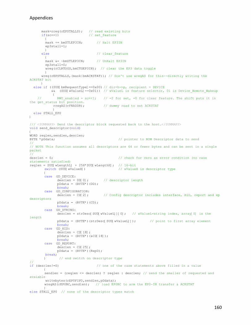
Appendices
160
mask=rreg(rEPSTALLS); // read existing bits
if(sc==1) // set_feature
{
mask += bmSTLEP3IN; // Halt EP3IN
ep3stall=1;
}
else // clear_feature
{
mask &= ~bmSTLEP3IN; // UnHalt EP3IN
ep3stall=0;
wreg(rCLRTOGS,bmCTGEP3IN); // clear the EP3 data toggle
}
wreg(rEPSTALLS,(mask|bmACKSTAT)); // Don't use wregAS for this--directly writing the
ACKSTAT bit
}
else if ((SUD[bmRequestType]==0x00) // dir=h->p, recipient = DEVICE
&& (SUD[wValueL]==0x01)) // wValueL is feature selector, 01 is Device_Remote_Wakeup
{
// RWU_enabled = sc<<1; // =2 for set, =0 for clear feature. The shift puts it in
the get_status bit position.
rregAS(rFNADDR); // dummy read to set ACKSTAT
}
else STALL_EP0
}
/// <SUMMARY> Send the descriptor block requested back to the host.</SUMMARY>
void send_descriptor(void)
{
WORD reqlen,sendlen,desclen;
BYTE *pDdata; // pointer to ROM Descriptor data to send
//
// NOTE This function assumes all descriptors are 64 or fewer bytes and can be sent in a single
packet
//
desclen = 0; // check for zero as error condition (no case
statements satisfied)
reqlen = SUD[wLengthL] + 256*SUD[wLengthH]; // 16-bit
switch (SUD[wValueH]) // wValueH is descriptor type
{
case GD_DEVICE:
desclen = DD[0]; // descriptor length
pDdata = (BYTE*)(DD);
break;
case GD_CONFIGURATION:
desclen = CD[2]; // Config descriptor includes interface, HID, report and ep
descriptors
pDdata = (BYTE*)(CD);
break;
case GD_STRING:
desclen = strDesc[SUD[wValueL]][0]; // wValueL=string index, array[0] is the
length
pDdata = (BYTE*)(strDesc[SUD[wValueL]]); // point to first array element
break;
case GD_HID:
desclen = CD[18];
pDdata = (BYTE*)(&CD[18]);
break;
case GD_REPORT:
desclen = CD[25];
pDdata = (BYTE*)(RepD);
break;
} // end switch on descriptor type
//
if (desclen!=0) // one of the case statements above filled in a value
{
sendlen = (reqlen <= desclen) ? reqlen : desclen; // send the smaller of requested and
avaiable
writebytes(rEP0FIFO,sendlen,pDdata);
wregAS(rEP0BC,sendlen); // load EP0BC to arm the EP0-IN transfer & ACKSTAT
}
else STALL_EP0 // none of the descriptor types match
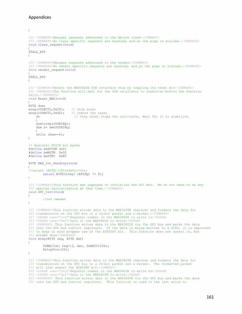
Appendices
161
}
/// <SUMMARY>Manages requests addressed to the device class</SUMMARY>
/// <REMARKS>No class specific requests are handled, and so the pipe is stalled.</REMARKS>
void class_request(void)
{
STALL_EP0
}
/// <SUMMARY>Manages requests addressed to the vendor</SUMMARY>
/// <REMARKS>No vendor specific requests are handled, and so the pipe is stalled.</REMARKS>
void vendor_request(void)
{
STALL_EP0
}
/// <SUMMARY>Resets the MAX3420E USB interface chip by toggling its reset bit</SUMMARY>
/// <REMARKS>The function will wait for the USB oscillator to stabilize before the function
exits.</REMARKS>
void Reset_MAX(void)
{
BYTE dum;
wreg(rUSBCTL,0x20); // chip reset
wreg(rUSBCTL,0x00); // remove the reset
do // Chip reset stops the oscillator. Wait for it to stabilize.
{
dum=rreg(rUSBIRQ);
dum &= bmOSCOKIRQ;
}
while (dum==0);
}
// Register SPICN bit masks
#define bmSPIEN 0x01
#define bmMSTM 0x02
#define bmSTBY 0x80
BYTE MAX_Int_Pending(void)
{
//return (BYTE)((PI6&0x01)==0);
return BYTE(rreg( rEPIRQ) != 0);
}
/// <SUMMARY>This function was supposed to initialize the SPI Bus. We do not need to do any
/// special initialization at this time.</SUMMARY>
void SPI_Init(void)
{
//not needed
}
/// <SUMMARY>This function writes data to the MAX3420E register and formats the data for
/// transmission on the SPI bus in a 16-bit packet and a marker.</SUMMARY>
/// <PARAM name="reg">Register number in the MAX3420E to write to</PARAM>
/// <PARAM name="dat">Data in the MAX3420E to write</PARAM>
/// <REMARKS> This function writes data to the MAX3420E via the SPI bus and packs the data
/// into the SPI bus control registers. If the data is being written to a FIFO, it is important
/// to keep in mind propper use of the ACKSTAT bit. This function does not assert it, but
/// wregAS does</REMARKS>
void wreg(BYTE reg, BYTE dat)
{
USBWrite( reg>>3, dat, 0xABCC1234);
DelayProc(25);
}
/// <SUMMARY>This function writes data to the MAX3420E register and formats the data for
/// transmission on the SPI bus in a 16-bit packet and a marker. The formatted packet
/// will also assert the ACKSTAT bit</SUMMARY>
/// <PARAM name="reg">Register number in the MAX3420E to write to</PARAM>
/// <PARAM name="dat">Data in the MAX3420E to write</PARAM>
/// <REMARKS> This function writes data to the MAX3420E via the SPI bus and packs the data
/// into the SPI bus control registers. This function is used in the last write to

Appendices
162
/// the FIFO in response to a USB bus request</REMARKS>
void wregAS(BYTE reg, BYTE dat)
{
USBWriteAS( reg>>3, dat, 0xABCE1234);
DelayProc(25);
}
// Read a register, return its value.
BYTE rreg(BYTE reg)
{
USBRead( reg>>3, 0xABCD1234);
DelayProc(25);
UINT nResult = FPGARead(0x0800000e);//0x0800000e
return (nResult & 0xFF);
}
// Read a byte (as rreg), but also set the AckStat bit in the command byte.
BYTE rregAS(BYTE reg)
{
USBReadAS( reg>>3, 0xABCF1234);
DelayProc(25);
UINT nResult = FPGARead(0x0800000e);//0x0800000e
return (nResult & 0xFF);
}
void readbytes(BYTE reg, BYTE N, BYTE *p)
{
BYTE j;
for(j=0; j<N; j++)
{
*p = rreg(reg);
p++; // bump the pointer
}
}
void writebytes(BYTE reg, BYTE N, BYTE *p)
{
BYTE j,wd;
for(j=0; j<N; j++)
{
wd = *p; // write the array value
wreg( reg, wd );
p++; // bump the pointer
}
}
//
// Diagnostic Aid:
// Call this function from main() to verify operation of your SPI port.
//
void test_SPI(void) // Use this to check your versions of the rreg and wreg functions
{
BYTE j,wr,rd;
SPI_Init(); // Configure and initialize the uP's SPI port
wreg(rPINCTL,bmFDUPSPI); // MAX3420: SPI=full-duplex
wreg(rUSBCTL,bmCHIPRES); // reset the MAX3420E
wreg(rUSBCTL,0); // remove the reset
wr=0x01; // initial register write value
for(j=0; j<8; j++)
{
wreg(rUSBIEN,wr);
rd = rreg(rUSBIEN);
wr <<= 1; // Put a breakpoint here. Values of 'rd' should be 01,02,04,08,10,20,40,80
}
}

Appendices
163
Parameter Header File
#ifndef _VPT_H_PARAMETERS_
#define _VPT_H_PARAMETERS_
#endif
//Modulation
////////////////////////////////////////////////////////
//PFPGA_REGISTER Duty_Reg; //duty cycle
//PFPGA_REGISTER DeadTime_Reg; //deadtime
//PFPGA_REGISTER PD_Reg; //pulse deletion
//PFPGA_REGISTER SwPer_Reg; //switching period
//PFPGA_REGISTER Mod_Sel_Reg; //modulation method
//PFPGA_REGISTER Curr_Dir_Reg; //current direction
//ADC Scaling
////////////////////////////////////////////////////////
static const float CHC1_CHA_SCALE=205; //AC Volt
static const float CHC1_CHB_SCALE=205; //DC Bus
static const float CHC2_CHA_SCALE=205; //AC Curr
static const float CHC2_CHB_SCALE=205; //HS Temp
static const float CHC1_CHA_OFFSET=1; //AC Volt
static const float CHC1_CHB_OFFSET=-1; //DC Bus
static const float CHC2_CHA_OFFSET=1; //AC Curr
static const float CHC2_CHB_OFFSET=0; //HS Temp
// Constant Value
/////////////////////////////////////////////////////////
static const float Period=50e-6; //switching period
static const float pi=3.14159265358979; //pi
static const float twopi=6.28318530717958; //2*pi
static const float TimeInc=50e-6; //imcrement of Time for every INT, 50us=20khz,
100us=10khz
static const float sqrt_2 = 1.41421356237309;
static const float sqrt3_2 = 0.86602540378443;
static float Time=0;
static float InitTime=0; // for open loop test
static float Mod_indexopen=0; // open loop test modulation index
int Open_Close_Sel; //if =1 =>open loop, if =0 =>closed loop
float Duty_ab; // calculated duty cycle
//static const float linefreq=60; // line angle freq
float linefreq = 60.0;
static float f_line = 60.0;
int DTC_OnOff = 0;
int ff_state = 1;
int Dump_Mem = 0;
int sync_cmd = 0;
int track_grid = 0;
//Counter Value
////////////////////////////////////////////////////////////
static const int bitPer=4000; //4000=20khz, 8000=10khz
static const int bitDAC=4096;
//sensored signal
//////////////////////////////////////////////////////////////
static float Vdc; // DC bus volt
static float Vac; // grid volt
static float Vac_grid; // grid volt
static float Iac; // grid current
static float Charge_I; // Idc (+/-) to/from battery
static float Vac1 = 0; // test grid volt
static float Iac1 = 0; // test grid current
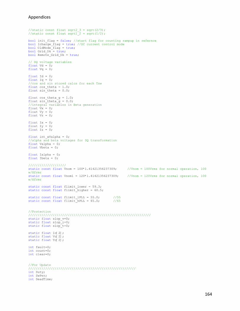
Appendices
164
//static const float sqrt2_3 = sqrt(2/3);
//static const float sqrt1_2 = sqrt(1/2);
bool init_flag = false; //start flag for counting rampup in refernce
bool Icharge_flag = true; //DC current control mode
bool OldMode_flag = true;
bool Grid_Ok = true;
bool Remote_Grid_Ok = true;
// DQ voltage variables
float Vd = 0;
float Vq = 0;
float Id = 0;
float Iq = 0;
//cos and sin stored calcs for each Tsw
float cos_theta = 1.0;
float sin_theta = 0.0;
float cos_theta_g = 1.0;
float sin_theta_g = 0.0;
//integral variables in Beta generation
float Vx = 0;
float Vy = 0;
float Vz = 0;
float Ix = 0;
float Iy = 0;
float Iz = 0;
float int_wValpha = 0;
//alpha and beta voltages for DQ transformation
float Valpha = 0;
float Vbeta = 0;
float Ialpha = 0;
float Ibeta = 0;
////////////////////
static const float Vnom = 100*1.41421356237309; //Vnom = 100Vrms for normal operation, 100
w/Xfrmr
static const float Vnom1 = 120*1.41421356237309; //Vnom = 120Vrms for normal operation, 100
w/Xfrmr
static const float flimit_lower = 59.3;
static const float flimit_higher = 60.5;
static const float flimit_lPLL = 55.0; //55
static const float flimit_hPLL = 65.0; //65
//Protection
/////////////////////////////////////////////////////////////////
static float slop_v=0;
static float slop_i=0;
static float slop_t=0;
static float Ic[2];
static float Vc[2];
static float Tc[2];
int fault=0;
int count=0;
int clear=0;
//For Update
/////////////////////////////////////////////////////////
int Duty;
int SwPer;
int DeadTime;

Appendices
165
int Mod_Sel;
int Curr_Dir;
int PD;
//int DTC_OnOff;
//Look_up value
//////////////////////////////////////////////////////////////
float Vdc_look[100];
float Iac_look[100];
float Vac_look[100];
//LOW PASS FILTER fc=1/pi*fs
///////////////////////////////////////////////////////////
float LPF_a1=0.5;
float LPF_a2=0.5;
float Vdc_I[2]={0,0};
float Vac_I[2]={0,0};
float Iac_I[2]={0,0};
float Vdc_filter;
float Iac_filter;
float Vac_filter;
//Controller Part
////////////////////////////////////////////////////////
static float Vdc_ref=340;
float Vdc_err;
float phasor;
float Iac_ref;
float Iac_refPQ;
float Iac_ref1;
float Iac_mag;
float Iac_err;
float Vdref;
float Imag = 0;
//PI Parameters
/////////////////////////////////////////////////////////////
float V_P;
float V_I;
float I_acmag[2]={0,0};
float Vdc_err_I[2]={0,0};
float I_P;
float I_I;
float Dab[2]={0,0};
float Iac_err_I[2]={0,0};
float a1=0.00125;
float a2=-0.00075;
//////////////////
float yy=0;
float y=0;
float y_delta=0;
float yu_s=0;
float yu=0;
float K_anti=10;
float Current_I=1;//20;
float Current_P=0.006;//0.00538;
///////////////////
float Vmag=0;
float Vac_ref=0;
float Vac_err=0;
float yvy=0;
//float yv=0;
float yv_delta=0;
float yvu_s=0;
float yvu=0;
float Voltage_I=15;
float Voltage_P=5;
float yc[4]={0,0,0,0};

Appendices
166
float xc[4]={0,0,0,0};
float yv[5]={0,0,0,0,0};
float yv_inv[5]={0,0,0,0,0};
float yv_rec[5]={0,0,0,0,0};
float yv_iDC[5]={0,0,0,0,0};
float yv1=0;
float xv_inv[5]={0,0,0,0,0};
float xv_rec[5]={0,0,0,0,0};
//Data Check
////////////////////////////////////////////////////////////////
float Vdc_check[1000];
float Iac_check[1000];
float Vac_check[1000];
float Vacg_check[1000];
float Ierr_check[1000];
float Dab_check[1000];
float Iref_check[100];
float Vd_check[1000];
float Vq_check[1000];
float Id_check[1000];
float Iq_check[1000];
float Valpha_check[1000];
float Vbeta_check[1000];
float Ialpha_check[1000];
float Ibeta_check[1000];
float Sg_check[1000];
float Pg_check[1000];
float Qg_check[1000];
float w_check[1000];
float P_check[1000];
float Q_check[1000];
int index=0;
int index2=0;
int index_PLL=0;
int counter_check=0;
int cntr_trackGrid = 0;
//PLL
/////////////////////////////////////////////////////////////////
float theta=0;
float theta_g=0;
float Err_PLL=0;
float Err_PLL_g=0;
float Int_Vac_PLL=0;
float Pro_Vac_PLL=0;
float Int_Vac_PLL_g=0;
float Pro_Vac_PLL_g=0;
float w=0;
float w_g=0;
//float Kp_PLL=15;
//float Ki_PLL=500;
float Kp_PLL=32.7; //54.5;//32.7;//21.8;//15;
float Ki_PLL=1232.76; //2054.6;//1232.76;//821.84;//500;
float Kp_PLL_g=32.7; //21.8;//15;
float Ki_PLL_g=1232.76; //821.84;//500;
Appendices
167
float theta_ac = 0;
/////////////////////Debug
int flag=0;
int old_relay;
double KK=0;
//////////////////////////USB COMMUNICATION/////////////////////
int MODE_STATUS = 0;
int ACTIVE_POWER = 0;
int REACTIVE_POWER = 0;
int MODE_DEMAND = 0x01111111;
int P_DEMAND = 0;
int Q_DEMAND = 0;
int VOLTAGE = 120;//0//120Vrms
float Voltage1 = 120;
float Voltage2 = 120;
int FREQ = 60000;//0;//60000mHz
float Freq1 = 60000;
float Freq2 = 60.0;
int CHARGE_STATUS = 0;
int GRID_MODE = 0;
//////////////////////////
float I_DCref = 0; //Charge current reference
float I_DCref_comand=0; //charge current calculated from higher controller
int Charge_flag = 0;
int Charge_flag1 = 0;
int Charge_flag2 = 0;
int Charge_flag3 = 0;
int StopCharge_flag = 0;
float PF_Multiplier = 0;
float PF_Angle = 0.0;
float PF_AngleCmd = 0.0;
int DC_Current_Command = 0;
int Batt_SOC = 0;
int flag_mode = 0;
float P_d = 0.0;
float Q_d = 0.0;
float S_d = 0.0;
float S_g = 0;
int signP_g = 1;
/*
const static float A1_LPF = 1.9925;
const static float A2_LPF = -0.9925;
const static float A3_LPF = 1.0;
const static float A4_LPF = 0.0;
const static float B1_LPF = 0.003906;
const static float B2_LPF = 0.0;
const static float C1_LPF = 0.00181;
const static float C2_LPF = 0.00181;
float X1_LPF = 104141.1929;
float X2_LPF = 104141.1929;
*/
const static float A1_LPF = 0.99968589007750;
const static float B1_LPF = 0.01562500000000;
const static float C1_LPF = 0.02010303504027;
float X1_LPF = 0.0;
float X2_LPF = 0.0;
float X3_LPF = 0.0;
float X4_LPF = 0.0;
float Xw_LPF = 0.0;

Appendices
168
float VdLPF = 0.0;
float VqLPF = 0.0;
float IdLPF = 0.0;
float IqLPF = 0.0;
float wLPF = 376.9911184;
float Int_Vac_PLL_d = 0;
float Pro_Vac_PLL_d = 0;
float Int_Vac_PLL_q = 0;
float Pro_Vac_PLL_q = 0;
float Vac_err_d = 0;
float Vac_err_q = 0;
float P_dcRef = 0.0;
float S_limit = 1.6e3;
const static float DutyHPF_A = -62.83185307179586;
const static float DutyHPF_B = 8.0;
const static float DutyHPF_C = -7.85398163397448;
const static float DutyHPF_D = 1.0;
float DutyHPF_X = 0.0;

Appendices
169
Functions Header File
#ifndef _VPT_H_FUNCTIONS_
#define _VPT_H_FUNCTIONS_
void ConfigurePWM(void);
void irq0_handler(int); // interrupt routine
void ADScale(void); // read ADC value
void Ramp_vref(void); //
void Ramp_iref(void);
void Ramp_Ref(float, float, float);
void Openloop(void); // Openloop controller
void Closedloop(void); // Closedloop controller
void Update(void); // update value to FPGA
void Protection(void); //overvoltage, overcurrent, overtemp protection
void Isl_Detect(const float, const float, const float, bool, bool);
void DQ_TransformV(const float, const float, float, float);
void DQ_TransformI(const float, const float, float, float);
void PLL(void);
void PLL_grid(void);
void PLL_sync(void);
void PLL1(void);
void ChargeCurrentRef(void);
void StateOfCharge(void);
void Power_Calc(void);
void PowerRef_Calc(void);
void Vac_PI_Comp(void);
#endif

Appendices
170
UControl Header File
//
#ifndef __UCONTROL_H__
#define __UCONTROL_H__
#endif //#ifndef __UCONTROL_H__
/////////////////////////////////////////////////////////////////////
typedef unsigned int UINT;
typedef volatile UINT FPGA_ACCESS;
typedef FPGA_ACCESS* const PFPGA_REGISTER;
//Modulator
static PFPGA_REGISTER g_cpwDuty = (UINT*)(0x08000014);
static PFPGA_REGISTER g_cpwDeadtime = (UINT*)(0x08000016);
static PFPGA_REGISTER g_cpwPD = (UINT*)(0x0800001A);
static PFPGA_REGISTER g_cpwPer = (UINT*)(0x08000018);
static PFPGA_REGISTER g_cpwMod_SEL = (UINT*)(0x08000010);
static PFPGA_REGISTER g_cpwCurr_Dir = (UINT*)(0x08000012);
static PFPGA_REGISTER g_cpwDeadCom = (UINT*)(0x0800003A);
//AD Channel
static PFPGA_REGISTER reg_ADC1CHA = (UINT*)(0x0800003C);
static PFPGA_REGISTER reg_ADC1CHB = (UINT*)(0x0800003E);
static PFPGA_REGISTER reg_ADC1CHC = (UINT*)(0x08000042);
static PFPGA_REGISTER reg_ADC1CHD = (UINT*)(0x08000044);
static PFPGA_REGISTER reg_ADC2CHA = (UINT*)(0x08000046);
static PFPGA_REGISTER reg_ADC2CHB = (UINT*)(0x08000048);
static PFPGA_REGISTER reg_ADC2CHC = (UINT*)(0x0800004A);
static PFPGA_REGISTER reg_ADC2CHD = (UINT*)(0x0800004C);
static PFPGA_REGISTER reg_ADAV = (UINT*)(0x0800004E);
//DCA Channel
static PFPGA_REGISTER g_cpwDACCTL = (UINT*)(0x08000004);
static PFPGA_REGISTER g_cpwDACCHA = (UINT*)(0x02000000);
static PFPGA_REGISTER g_cpwDACCHB = (UINT*)(0x02000002);
/////////////////////////////////////////////////////////////////////////////////////
static PFPGA_REGISTER relay = (UINT*)(0x0800001C);
static PFPGA_REGISTER reset_ff= (UINT*)(0x0800001E);
static PFPGA_REGISTER reset_ff2= (UINT*)(0x08000034);
static PFPGA_REGISTER reset_ff3= (UINT*)(0x08000036);
static PFPGA_REGISTER HSFan= (UINT*)(0x08000038);

References
171
References
[1] F. Blaabjerg, et al., "Overview of Control and Grid Synchronization for Distributed Power Generation Systems," Industrial Electronics, IEEE Transactions on, vol. 53, pp. 1398-1409, 2006.
[2] G. Joos, et al., "The potential of distributed generation to provide ancillary services," in Power Engineering Society Summer Meeting, 2000. IEEE, Seattle, WA, 2000, pp. 1762-1767 vol. 3.
[3] S. Barsali, et al., "Operating and planning issues of distribution grids containing diffuse generation," in Electricity Distribution, 2001. Part 1: Contributions. CIRED. 16th International Conference and Exhibition on (IEE Conf. Publ No. 482), Amsterdam, 2001, p. 5 pp. vol.4.
[4] P. A. Daly and J. Morrison, "Understanding the potential benefits of distributed generation on power delivery systems," in Rural Electric Power Conference, 2001, Little Rock, AR, 2001, pp. A2/1-A213.
[5] R. Lawrence and S. Middlekauff, "Distributed generation: the new guy on the block," in Petroleum and Chemical Industry Conference, 2003. Record of Conference Papers. IEEE Industry Applications Society 50th Annual, 2003, pp. 223-228.
[6] R. Teodorescu and F. Blaabjerg, "Flexible control of small wind turbines with grid failure detection operating in stand-alone and grid-connected mode," Power Electronics, IEEE Transactions on, vol. 19, pp. 1323-1332, 2004.
[7] "Functional Specification For Community Energy Storage (CES) Unit," American Electric Power, Project SpecificationJuly 2009 2009.
[8] D. T. Ton, et al., "Solar Energy Grid Integration Systems – Energy Storage (SEGIS-ES)," U.S. Department of Energy, Sandia National Laboratories, Technical ReportJuly 2008 2008.
[9] "IEEE Standard for Interconnecting Distributed Resources with Electric Power Systems," 2003.
[10] REN21, "Renewables Global Status Report: 2009 Update," Renewable Energy Policy Network for the 21st Century, Paris, 2009.
[11] D. Calef and R. Goble, "The allure of technology: How France and California promoted electric and hybrid vehicles to reduce urban air pollution," Policy Sci, vol. 40, p. 34, March 2007 2007.
[12] PJM, "Renewable Energy Dashboard," PJM, 2009. [13] PJM, "A Greener Grid," PJM, 2009. [14] K. Parks, et al., "Cost and Emissions Associated with Plug-in Hybrid Electric Vehicle
Charging in the Xcel Energy Colorodo Service Territory," National Renewable Energy Laboratory, May 2007.
[15] "The SMART GRID: An Introduction.," Department of Energy, 2009. [16] B. K. Sovacool and R. F. Hirsh, "Beyond batteries: An examination of the benefits and
barriers to plug-in hybrid electric vehicles (PHEVs) and a vehicle-to-grid (V2G) transition," Energy Policy, vol. 37, pp. 1095-1103, 2009.

References
172
[17] W. Kempton and J. Tomic, "Vehicle-to-grid power fundamentals: Calculating capacity and net revenue," Journal of Power Sources, vol. 144, pp. 268-279, 2005.
[18] W. Kempton and J. Tomic, "Vehicle-to-grid power implementation: From stabilizing the grid to supporting large-scale renewable energy," Journal of Power Sources, vol. 144, pp. 280-294, 2005.
[19] R. F. Hirsh and B. K. Sovacool, "Technological Systems and Momentum Change: American Electric Utilities, Restructuring, and Distributed Generation Technologies," The Journal of Technology Studies, vol. 32, pp. 72-85, Spring 2006 2006.
[20] R. Badinelli, et al., "DESIGNING A SECURE AND EFFICIENT DISTRIBUTED GENERATION POWER SYSTEM: POLICY, CONSUMER AFFAIRS, AND COMPUTER SIMULATION ISSUES," National Science Foundation - Electric Power Networks Efficiency and Security, Arlington, VA, Summer 2005 2005.
[21] IEA, "Distributed Generation in Liberalized Electricity Markets," International Energy Agency, Paris, France, 2002.
[22] US-EPA, "National Air Quality - Status and Trends through 2007," U.S. Environmental Protection Agency, Research Triangle Park, NC, November 2008 2008.
[23] EPRI, "The Cost of Power Disturbances to Industrial and Digital Economy Companies," Electric Power Research Institute, 2001.
[24] W. Kempton, et al., "Vehicle-to-Grid Power: Battery, Hybrid, and Fuel Cell Vehicles as Resources for Distributed Electric Power in California," June 2001 2001.
[25] A. Engler and N. Soultanis, "Droop control in LV-Grids," in Future Power Systems, 2005 International Conference on, 2005, pp. 1-6.
[26] K. De Brabandere, et al., "A Voltage and Frequency Droop Control Method for Parallel Inverters," Power Electronics, IEEE Transactions on, vol. 22, pp. 1107-1115, 2007.
[27] M. N. Marwali, et al., "Stability Analysis of Load Sharing Control for Distributed Generation Systems," Energy Conversion, IEEE Transaction on, vol. 22, pp. 737-745, 2007.
[28] M. N. Marwali, et al., "Control of distributed generation systems - Part II: Load sharing control," Power Electronics, IEEE Transactions on, vol. 19, pp. 1551-1561, 2004.
[29] P. D. Roberts, "A brief overview of model predictive control," in Practical Experiences with Predictive Control (Ref. No. 2000/023), IEE Seminar on, 2000, pp. 1/1-1/3.
[30] D. Sprock and H. Ping, "Predictive discrete time control of switch-mode applications," in Power Electronics Specialists Conference, 1997. PESC '97 Record., 28th Annual IEEE, 1997, pp. 175-181 vol.1.
[31] J. Shih-Liang, et al., "A three-phase PWM AC-DC converter with low switching frequency and high power factor using DSP-based repetitive control technique," in Power Electronics Specialists Conference, 1998. PESC 98 Record. 29th Annual IEEE, 1998, pp. 517-523 vol.1.
[32] C. Rech, et al., "Analysis and design of a repetitive predictive-PID controller for PWM inverters," in Power Electronics Specialists Conference, 2001. PESC. 2001 IEEE 32nd Annual, 2001, pp. 986-991 vol.2.
[33] G. Weiss, et al., "H_inf repetitive control of DC-AC converters in microgrids," Power Electronics, IEEE Transactions on, vol. 19, pp. 219-230, 2004.

References
173
[34] P. Y. Tiwari and M. V. Kothare, "Repetitive Model Predictive Control using Linear Matrix Inequalities," in American Control Conference, 2008, 2008, pp. 63-68.
[35] M. S. Chen, et al., "Sliding mode control reduced chattering for with dependent uncertainties," in Networking, Sensing and Control, 2004 IEEE International Conference on, 2004, pp. 967-971 Vol.2.
[36] K. Jezernik and D. Zadravec, "Sliding mode controller for a single phase inverter," in Applied Power Electronics Conference and Exposition, 1990. APEC '90, Conference Proceedings 1990., Fifth Annual, 1990, pp. 185-190.
[37] J. Shih-Liang and T. Ying-Yu, "Discrete feedforward sliding mode control of a PWM inverter for sinusoidal output waveform synthesis," in Power Electronics Specialists Conference, PESC '94 Record., 25th Annual IEEE, 1994, pp. 552-559 vol.1.
[38] S. L. Jung and Y. Y. Tzou, "Sliding mode control of a closed-loop regulated PWM inverter under large load variations," in Power Electronics Specialists Conference, 1993. PESC '93 Record., 24th Annual IEEE, 1993, pp. 616-622.
[39] K. J. P. Macken, et al., "Distributed control of renewable generation units with integrated active filter," Power Electronics, IEEE Transactions on, vol. 19, pp. 1353-1360, 2004.
[40] A. Roshan, et al., "A D-Q Frame Controller for a Full-Bridge Single Phase Inverter Used in Small Distributed Power Generation Systems," in Applied Power Electronics Conference, APEC 2007 - Twenty Second Annual IEEE, 2007, pp. 641-647.
[41] K. P. Louganski and J.-S. Lai, "Reactive Power Control Realizations in Single-Phase Active-Front-End Converters," in Applied Power Electronics Conference, APEC 2007 - Twenty Second Annual IEEE, 2007, pp. 797-803.
[42] M. Saitou, et al., "A control strategy of single-phase active filter using a novel d-q transformation," in Industry Applications Conference, 2003. 38th IAS Annual Meeting. Conference Record of the, 2003, pp. 1222-1227 vol.2.
[43] M. Liserre, et al., "Design and control of a three-phase active rectifier under non-ideal operating conditions," in Industry Applications Conference, 2002. 37th IAS Annual Meeting. Conference Record of the, 2002, pp. 1181-1188 vol.2.
[44] D. R. Costa, Jr., et al., "Analysis and software implementation of a robust synchronizing circuit PLL circuit," in Industrial Electronics, 2003. ISIE '03. 2003 IEEE International Symposium on, 2003, pp. 292-297 vol. 1.
[45] G.-C. Hsieh and J. C. Hung, "Phase-locked loop techniques. A survey," Industrial Electronics, IEEE Transactions on, vol. 43, pp. 609-615, 1996.
[46] L. N. Arruda, et al., "Wide bandwidth single and three-phase PLL structures for grid-tied," in Photovoltaic Specialists Conference, 2000. Conference Record of the Twenty-Eighth IEEE, 2000, pp. 1660-1663.
[47] S. K. Chung, et al., "Precision control of single-phase PWM inverter using PLL compensation," Electric Power Applications, IEE Proceedings -, vol. 152, pp. 429-436, 2005.
[48] M. Ciobotaru, et al., "A New Single-Phase PLL Structure Based on Second Order Generalized Integrator," in Power Electronics Specialists Conference, 2006. PESC '06. 37th IEEE, 2006, pp. 1-6.

References
174
[49] K. De Brabandere, et al., "Design and Operation of a Phase-Locked Loop with Kalman Estimator-Based Filter for Single-Phase Applications," in IEEE Industrial Electronics, IECON 2006 - 32nd Annual Conference on, 2006, pp. 525-530.
[50] G. H. Jung, et al., "DSP based control of high power static VAr compensator using novel vector product phase locked loop," in Power Electronics Specialists Conference, 1996. PESC '96 Record., 27th Annual IEEE, 1996, pp. 238-243 vol.1.
[51] V. Kaura and V. Blasko, "Operation of a phase locked loop system under distorted utility conditions," Industry Applications, IEEE Transactions on, vol. 33, pp. 58-63, 1997.
[52] S. M. Silva, et al., "Performance evaluation of PLL algorithms for single-phase grid-connected systems," in Industry Applications Conference, 2004. 39th IAS Annual Meeting. Conference Record of the 2004 IEEE, 2004, pp. 2259-2263 vol.4.
[53] S. K. Chung, "Phase-locked loop for grid-connected three-phase power conversion systems," Electric Power Applications, IEE Proceedings-, vol. 147, pp. 213-219, 2000.
[54] S.-J. Lee, et al., "A new phase detecting method for power conversion systems considering distorted conditions in power system," in Industry Applications Conference, 1999. Thirty-Fourth IAS Annual Meeting. Conference Record of the 1999 IEEE, 1999, pp. 2167-2172 vol.4.
[55] A. Timbus, et al., "Synchronization Methods for Three Phase Distributed Power Generation Systems. An Overview and Evaluation," in Power Electronics Specialists Conference, 2005. PESC '05. IEEE 36th, 2005, pp. 2474-2481.
[56] S. M. Shahruz, "Novel phase-locked loops with enhanced locking capabilities," in American Control Conference, 2002. Proceedings of the 2002, 2002, pp. 4086-4091 vol.5.
[57] J. Park and F. Maloberti, "Fractional-N PLL with 90° phase shift lock and active switched-capacitor loop filter," in Custom Integrated Circuits Conference, 2005. Proceedings of the IEEE 2005, 2005, pp. 329-332.
[58] B.-Y. Bae and H. Byung-Moon, "Novel 3-phase phase-locked loop composed of adaptive linear combiner," in Power Electronics and Applications, 2007 European Conference on, 2007, pp. 1-10.
[59] H.-S. Song, et al., "Very fast phase angle estimation algorithm for a single-phase system having sudden phase angle jumps," in Industry Applications Conference, 2002. 37th IAS Annual Meeting. Conference Record of the, 2002, pp. 925-931 vol.2.
[60] S. Sarma, et al., "Phase-locked loop design for flexible mode tracking," in TENCON 2003. Conference on Convergent Technologies for Asia-Pacific Region, 2003, pp. 1277-1283 Vol.4.
[61] J. R. C. Piqueira, et al., "Considering double frequency terms from phase detectors in synchronous master-slave networks," in System Theory, 2006. SSST '06. Proceeding of the Thirty-Eighth Southeastern Symposium on, 2006, pp. 453-456.
[62] W. F. Egan, Phase-Lock Basics, 2nd ed.: Wiley-IEEE Press, 2007. [63] F. Gardner, Phaselock Techniques, 2nd ed. New York, NY: Wiley & Sons, 1979. [64] D. H. Wolaver, Phase-Locked Loop Circuit Design, 1st ed. Englewood Cliffs, NJ: Prentice
Hall, 1991. [65] R. E. Best, Phase-Locked Loops: Design, Simulation, and Applications, 6th ed.: McGraw
Hill, 2007.

References
175
[66] J. E. Kim and J. S. Hwang, "Islanding detection method of distributed generation units connected to power distribution system," in Power System Technology, 2000. Proceedings. PowerCon 2000. International Conference on, Perth, WA, 2000, pp. 643-647 vol.2.
[67] K. A. Nigim and Y. G. Hegazy, "Intention islanding of distributed generation for reliability enhancement," in Power Engineering Society General Meeting, 2003, IEEE, 2003, p. 2451 Vol. 4.
[68] T. Thacker, et al., "Implementation of control and detection algorithms for utility interfaced power conversion systems," in Applied Power Electronics Conference and Exposition, 2006. APEC '06. Twenty-First Annual IEEE, Dallas, TX, 2006, p. 6 pp.
[69] H. Zeineldin, et al., "Intentional islanding of distributed generation," in Power Engineering Society General Meeting, 2005. IEEE, 2005, pp. 1496-1502 Vol. 2.
[70] H. H. Zeineldin, et al., "Impact of DG interface control on islanding detection and nondetection zones," Power Delivery, IEEE Transactions on, vol. 21, pp. 1515-1523, 2006.
[71] S.-I. Jang and K.-H. Kim, "Development of a logical rule-based islanding detection method for distributed resources," in Power Engineering Society Winter Meeting, 2002. IEEE, 2002, pp. 800-806 vol.2.
[72] S.-I. Jang and K.-H. Kim, "An islanding detection method for distributed generations using voltage unbalance and total harmonic distortion of current," Power Delivery, IEEE Transactions on, vol. 19, pp. 745-752, 2004.
[73] Z. Ye, et al., "Evaluation of anti-islanding schemes based on nondetection zone concept," Power Electronics, IEEE Transactions on, vol. 19, pp. 1171-1176, 2004.
[74] Z. Ye, et al., "A new family of active antiislanding schemes based on DQ implementation for grid-connected inverters," in Power Electronics Specialists Conference, 2004. PESC 04. 2004 IEEE 35th Annual, 2004, pp. 235-241 Vol.1.
[75] H. H. Zeineldin, et al., "Islanding detection of inverter-based distributed generation," Generation, Transmission and Distribution, IEE Proceedings-, vol. 153, pp. 644-652, 2006.
[76] C. Jeraputra and P. N. Enjeti, "Development of a robust anti-islanding algorithm for utility interconnection of distributed fuel cell powered generation," Power Electronics, IEEE Transactions on, vol. 19, pp. 1163-1170, 2004.
[77] T. Thacker, et al., "Islanding Control of a Distributed Generation Unit's Power Conversion System to the Electric Utility Grid," in Power Electronics Specialists Conference, 2005. PESC '05. IEEE 36th, Recife, Brazil, 2005, pp. 210-216.
[78] Z. Chunjiang, et al., "A Novel Active Islanding Detection Method of Grid-connected Photovoltaic Inverters Based on Current-Disturbing," in Power Electronics and Motion Control Conference, 2006. IPEMC '06. CES/IEEE 5th International, 2006, pp. 1-4.
[79] G. Hernandez-Gonzalez and R. Iravani, "Current injection for active islanding detection of electronically-interfaced distributed resources," Power Delivery, IEEE Transactions on, vol. 21, pp. 1698-1705, 2006.
[80] C. Jeraputra, et al., "An improved anti-islanding algorithm for utility interconnection of multiple distributed fuel cell powered generations," in Applied Power Electronics

References
176
Conference and Exposition, 2005. APEC 2005. Twentieth Annual IEEE, 2005, pp. 103-108 Vol. 1.
[81] H. Karimi, et al., "Negative-Sequence Current Injection for Fast Islanding Detection of a Distributed Resource Unit," Power Electronics, IEEE Transactions on, vol. 23, pp. 298-307, 2008.
[82] C. G. Hochgraf, "Anti-Islanding Detection Scheme For Distributed Power Generation," USA Patent, 2003.
[83] V. John, et al., "Investigation of anti-islanding protection of power converter based distributed generators using frequency domain analysis," Power Electronics, IEEE Transactions on, vol. 19, pp. 1177-1183, 2004.
[84] L. A. C. Lopes and H. Sun, "Performance assessment of active frequency drifting islanding detection methods," Energy Conversion, IEEE Transaction on, vol. 21, pp. 171-180, 2006.
[85] J. Yin, et al., "A new total frequency deviation algorithm for anti-islanding protection in inverter-based DG systems," in Electrical and Computer Engineering, 2005. Canadian Conference on, 2005, pp. 570-573.
[86] M.-J. Ko, et al., "Simulation of Active Frequency Drift Adding Zero Current Method for Islanding Detection," in Power Electronics Specialists Conference, 2006. PESC '06. 37th IEEE, 2006, pp. 1-5.
[87] Z. Ye, et al., "Study and Development of Anti-Islanding Control for Grid-Connected Inverters," National Renewable Energy Laboratory, May 2004.
[88] R. M. Hudson, et al., "Design considerations for three-phase grid connected photovoltaic inverters," in Photovoltaic Specialists Conference, 2002. Conference Record of the Twenty-Ninth IEEE, 2002, pp. 1396-1401.
[89] R. M. Hudson, et al., "Implementation and testing of anti-islanding algorithms for IEEE 929-2000 compliance of single phase photovoltaic inverters," in Photovoltaic Specialists Conference, 2002. Conference Record of the Twenty-Ninth IEEE, 2002, pp. 1414-1419.
[90] G.-K. Hung, et al., "Automatic phase-shift method for islanding detection of grid-connected photovoltaic inverters," Energy Conversion, IEEE Transaction on, vol. 18, pp. 169-173, 2003.
[91] O. Usta, et al., "Analysis of out of phase reclosing required for the protection of dispersed storage and generation units," in Electrotechnical Conference, 1996. MELECON '96., 8th Mediterranean, 1996, pp. 742-745 vol.2.
[92] R. Tirumala, et al., "Seamless transfer of grid-connected PWM inverters between utility-interactive and stand-alone modes," in Applied Power Electronics Conference and Exposition, 2002. APEC 2002. Seventeenth Annual IEEE, 2002, pp. 1081-1086 vol.2.
[93] Z. Yao, et al., "A novel control strategy for grid-interactive inverter in grid-connected and stand-alone modes," in Applied Power Electronics Conference and Exposition, 2006. APEC '06. Twenty-First Annual IEEE, 2006, p. 5 pp.
[94] D. Dong, "Modeling and Control Design of a Bidirectional PWM Covnerter for Single-Phase Energy Systems," M.S., Center for Power Electronics Systems, Virginia Tech, Blacksburg, VA, 2009.
References
177
[95] T. Thacker, et al., "Phase-Locked Loops using State Variable Feedback for Single-Phase Converter Systems," in Applied Power Electronics Conference and Exposition, 2009. APEC 2009. Twenty-Fourth Annual IEEE, Washington, DC, 2009, pp. 864-870.
[96] L. G. B. Rolim, et al., "Analysis and Software Implementation of a Robust Synchronizing PLL Circuit Based on the pq Theory," Industrial Electronics, IEEE Transactions on, vol. 53, pp. 1919-1926, 2006.
[97] J. Suonan, et al., "A Novel Single-Phase Adaptive Reclosure Scheme for Transmission Lines With Shunt Reactors," Power Delivery, IEEE Transactions on, vol. 24, pp. 545-551, 2009.
[98] T. Thacker, et al., "Single-Phase Islanding Detection based on Phase-Locked Loop Stability," in Energy Conversion Congress and Exposition, 2009. ECCE '09. 1st IEEE, San Jose, CA, 2009.
[99] K.-K. Shyu, et al., "Model Reference Adaptive Control Design for a Shunt Active-Power-Filter System," Industrial Electronics, IEEE Transactions on, vol. 55, pp. 97-106, 2008.
[100] H. H. Zeineldin and J. L. Kirtley, "Performance of the OVP/UVP and OFP/UFP Method With Voltage and Frequency Dependent Loads," Power Delivery, IEEE Transactions on, vol. 24, pp. 772-778, 2009.
[101] H.-B. Shin, "New antiwindup PI controller for variable-speed motor drives," Industrial Electronics, IEEE Transactions on, vol. 45, pp. 445-450, 1998.
[102] G. Francis, "A Synchronous Distributed Digital Control Architecture for High Power Converters," M.S.E.E., Center for Power Electronics Systems, Virginia Tech, Blacksburg, VA, 2004.
[103] A. Roshan, "A DQ ROTATING FRAME CONTROLLER FOR SINGLE PHASE FULL-BRIDGE INVERTERS USED IN SMALL DISTRIBUTED GENERATION SYSTEMS," M.S.E.E., Center for Power Electronics Systems, Virginia Tech, Blacksburg, VA, 2006.