Embed Size (px)
Citation preview
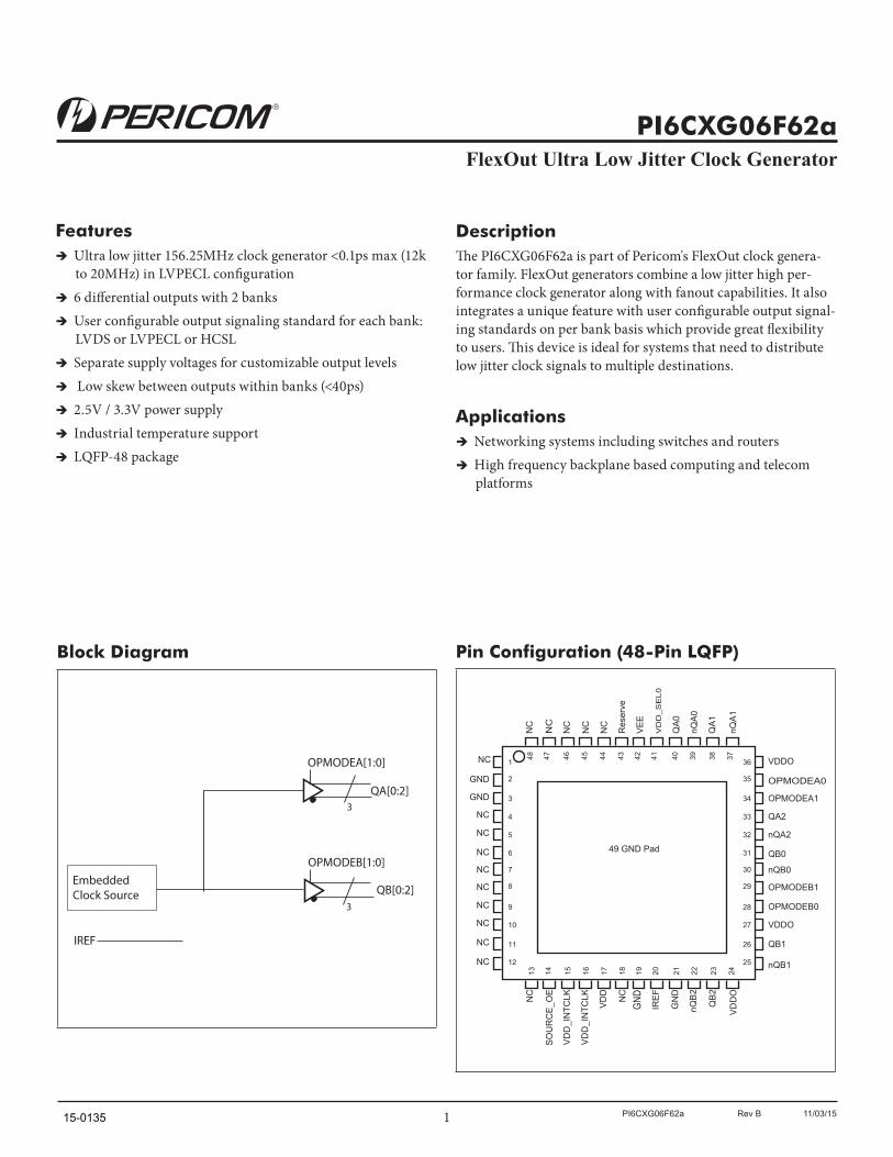
1 PI6CXG06F62a Rev B 11/03/15
PI6C20800B
FeaturesÎÎ Ultra low jitter 156.25MHz clock generator <0.1ps max (12k
to 20MHz) in LVPECL configuration ÎÎ 6 differential outputs with 2 banksÎÎ User configurable output signaling standard for each bank:
LVDS or LVPECL or HCSLÎÎ Separate supply voltages for customizable output levelsÎÎ Low skew between outputs within banks (<40ps)ÎÎ 2.5V / 3.3V power supplyÎÎ Industrial temperature supportÎÎ LQFP-48 package
PI6CXG06F62a
Block Diagram Pin Configuration (48-Pin LQFP)
DescriptionThe PI6CXG06F62a is part of Pericom's FlexOut clock genera-tor family. FlexOut generators combine a low jitter high per-formance clock generator along with fanout capabilities. It also integrates a unique feature with user configurable output signal-ing standards on per bank basis which provide great flexibility to users. This device is ideal for systems that need to distribute low jitter clock signals to multiple destinations.
ApplicationsÎÎ Networking systems including switches and routersÎÎ High frequency backplane based computing and telecom
platforms
FlexOut Ultra Low Jitter Clock Generator
1
2
3
NC 4
NC 5
6
NC
7
8
NC
NC
NC
GND
VD
D_I
NTC
LK
VD
D
VD
D_I
NTC
LK
GN
D
GND
nQB
2
NC
SO
UR
CE
_OE
9
10
11
12
13 14 15 16 17 18 19 20 21 22 23 24
36
35
34
33
32
31
30
29
28
27
26
25
48 47 46 45 44 43 42 41 40 39 38 37
NC
NC
NC
NC
NC
IRE
F
QB
2
VD
DO
QA2
nQA2
OPMODEA1
OPMODEB0
nQB0
VDDO
VDDO
OPMODEA0
QB0
OPMODEB1
QB1
nQB1
NC
Res
erve
NC
nQA
0
VD
D_
SE
L0
NC
NC
NC
VE
E
QA
0
QA
1
nQA
1
GND
49 GND Pad
Embedded Clock Source
IREF
3QA[0:2]
QB[0:2]
OPMODEA[1:0]
OPMODEB[1:0]
3
15-0135
2 PI6CXG06F62a Rev B 11/03/15
PI6CXG06F62a FlexOut Ultra Low Jitter Clock Generator
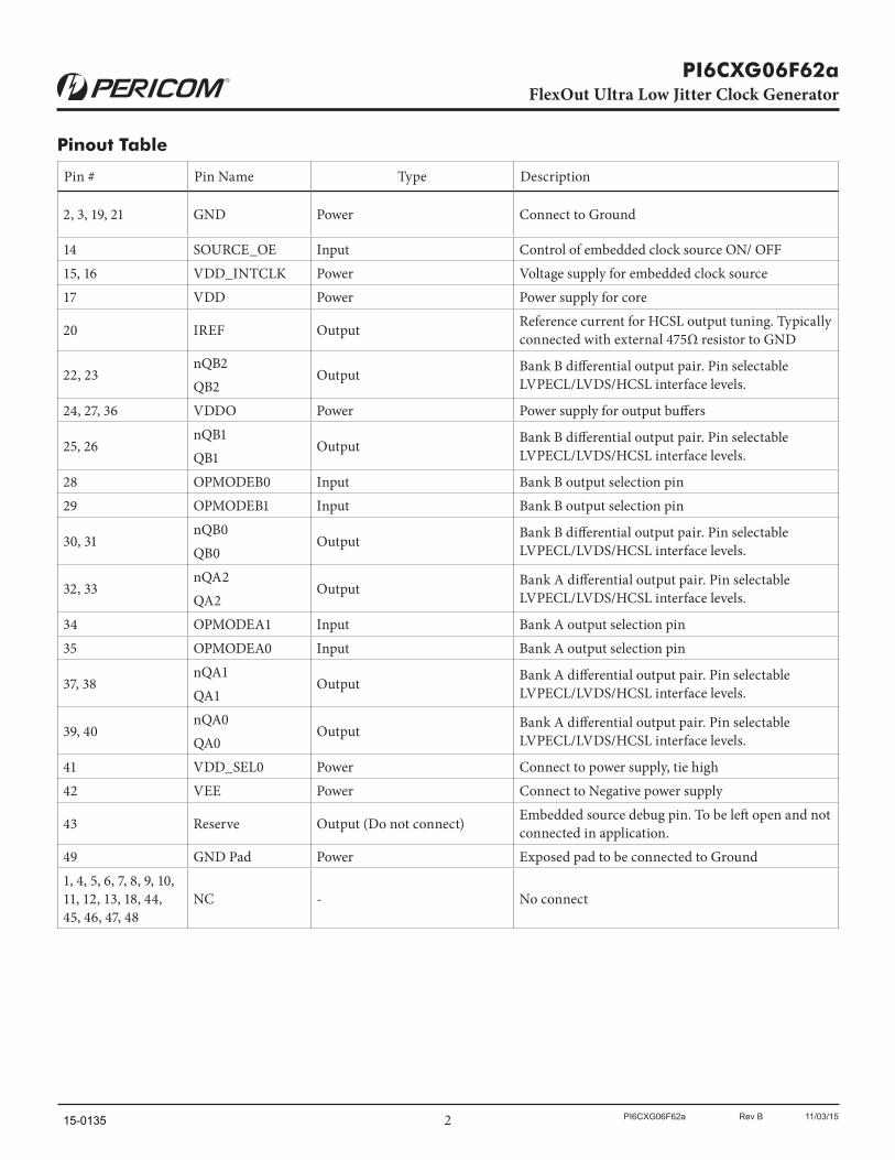
Pin # Pin Name Type Description
2, 3, 19, 21 GND Power Connect to Ground
14 SOURCE_OE Input Control of embedded clock source ON/ OFF15, 16 VDD_INTCLK Power Voltage supply for embedded clock source17 VDD Power Power supply for core
20 IREF Output Reference current for HCSL output tuning. Typically connected with external 475Ω resistor to GND
22, 23nQB2QB2
Output Bank B differential output pair. Pin selectable LVPECL/LVDS/HCSL interface levels.
24, 27, 36 VDDO Power Power supply for output buffers
25, 26nQB1QB1
Output Bank B differential output pair. Pin selectable LVPECL/LVDS/HCSL interface levels.
28 OPMODEB0 Input Bank B output selection pin29 OPMODEB1 Input Bank B output selection pin
30, 31nQB0QB0
Output Bank B differential output pair. Pin selectable LVPECL/LVDS/HCSL interface levels.
32, 33nQA2QA2
Output Bank A differential output pair. Pin selectable LVPECL/LVDS/HCSL interface levels.
34 OPMODEA1 Input Bank A output selection pin35 OPMODEA0 Input Bank A output selection pin
37, 38nQA1QA1
Output Bank A differential output pair. Pin selectable LVPECL/LVDS/HCSL interface levels.
39, 40nQA0QA0
Output Bank A differential output pair. Pin selectable LVPECL/LVDS/HCSL interface levels.
41 VDD_SEL0 Power Connect to power supply, tie high42 VEE Power Connect to Negative power supply
43 Reserve Output (Do not connect) Embedded source debug pin. To be left open and not connected in application.
49 GND Pad Power Exposed pad to be connected to Ground1, 4, 5, 6, 7, 8, 9, 10, 11, 12, 13, 18, 44, 45, 46, 47, 48
NC - No connect
Pinout Table
15-0135
3 PI6CXG06F62a Rev B 11/03/15
PI6CXG06F62a FlexOut Ultra Low Jitter Clock Generator
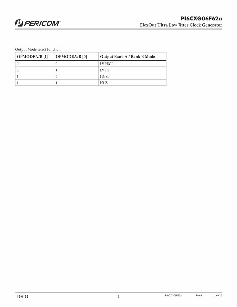
Output Mode select function
OPMODEA/B [1] OPMODEA/B [0] Output Bank A / Bank B Mode
0 0 LVPECL0 1 LVDS1 0 HCSL1 1 Hi-Z
15-0135
4 PI6CXG06F62a Rev B 11/03/15
PI6CXG06F62a FlexOut Ultra Low Jitter Clock Generator
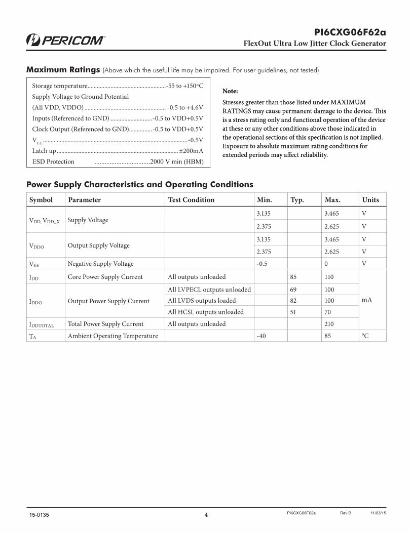
Maximum Ratings (Above which the useful life may be impaired. For user guidelines, not tested)
Storage temperature ...................................................-55 to +150ºC Supply Voltage to Ground Potential (All VDD, VDDO) ..................................................... -0.5 to +4.6VInputs (Referenced to GND) ...........................-0.5 to VDD+0.5V Clock Output (Referenced to GND)...............-0.5 to VDD+0.5V VEE ..............................................................................................-0.5VLatch up ............................................................................... ±200mA ESD Protection .................................2000 V min (HBM)
Note:
Stresses greater than those listed under MAXIMUM RATINGS may cause permanent damage to the device. This is a stress rating only and functional operation of the device at these or any other conditions above those indicated in the operational sections of this specification is not implied. Exposure to absolute maximum rating conditions for extended periods may affect reliability.
Power Supply Characteristics and Operating Conditions
Symbol Parameter Test Condition Min. Typ. Max. Units
VDD, VDD_X Supply Voltage3.135 3.465 V
2.375 2.625 V
VDDO Output Supply Voltage3.135 3.465 V
2.375 2.625 V
VEE Negative Supply Voltage -0.5 0 V
IDD Core Power Supply Current All outputs unloaded 85 110
mAIDDO Output Power Supply Current
All LVPECL outputs unloaded 69 100All LVDS outputs loaded 82 100
All HCSL outputs unloaded 51 70
IDDTOTAL Total Power Supply Current All outputs unloaded 210
TA Ambient Operating Temperature -40 85 °C
Note:
Stresses greater than those listed under MAXIMUM RATINGS may cause permanent damage to the device. This is a stress rating only and functional operation of the device at these or any other conditions above those indicated in the operational sections of this specification is not implied. Exposure to absolute maximum rating conditions for extended periods may affect reliability.
15-0135
5 PI6CXG06F62a Rev B 11/03/15
PI6CXG06F62a FlexOut Ultra Low Jitter Clock Generator
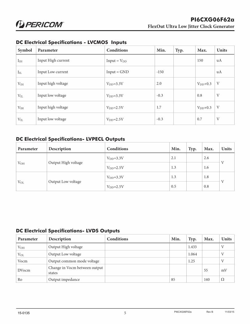
DC Electrical Specifications- LVPECL Outputs
Parameter Description Conditions Min. Typ. Max. Units
VOH Output High voltageVDD=3.3V 2.1 2.6
VVDD=2.5V 1.3 1.6
VOL Output Low voltage VDD=3.3V 1.3 1.8
VVDD=2.5V 0.5 0.8
DC Electrical Specifications - LVCMOS Inputs
Symbol Parameter Conditions Min. Typ. Max. Units
IIH Input High current Input = VDD 150 uA
IIL Input Low current Input = GND -150 uA
VIH Input high voltage VDD=3.3V 2.0 VDD+0.3 V
VIL Input low voltage VDD=3.3V -0.3 0.8 V
VIH Input high voltage VDD=2.5V 1.7 VDD+0.3 V
VIL Input low voltage VDD=2.5V -0.3 0.7 V
Parameter Description Conditions Min. Typ. Max. Units
VOH Output High voltage 1.433 V
VOL Output Low voltage 1.064 V
Vocm Output common mode voltage 1.25 V
DVocm Change in Vocm between output states 55 mV
Ro Output impedance 85 140 W
DC Electrical Specifications- LVDS Outputs
15-0135
6 PI6CXG06F62a Rev B 11/03/15
PI6CXG06F62a FlexOut Ultra Low Jitter Clock Generator
Parameter Description Conditions Min. Typ. Max. Units
VOH Output High voltage 520 800 mV
VOL Output Low voltage 0 150 mV
AC Electrical Specifications – Differential Outputs
Parameter Description Conditions Min. Typ. Max. Units
FOUT Clock output frequency 156.25 MHz
FSTAB Frequency stability ±25 ppm
Tr Output rise time From 20% to 80% 150 ps
Tf Output fall time From 80% to 20% 150 ps
TODC Output duty cycle Generator mode 48 52 %
VPP Output swing Single-endedLVPECL outputs 400
mVLVDS outputs 250HCSL outputs 520
TPHASEJ Phase jitter RMSLVPECL 0.07 0.1
psLVDS 0.09 0.12HCSL 0.09 0.15
VCROSS Absolute crossing voltage HCSL 160 460 mV
DVCROSS Total variation of crossing voltage HCSL 140 mV
TSK Output Skew 6 outputs devices, outputs in same bank, with same load, at DUT. 40 ps
TOD Valid to HiZ 200 ns
TOE HiZ to valid 200 ns
DC Electrical Specifications- HCSL Outputs
15-0135
7 PI6CXG06F62a Rev B 11/03/15
PI6CXG06F62a FlexOut Ultra Low Jitter Clock Generator
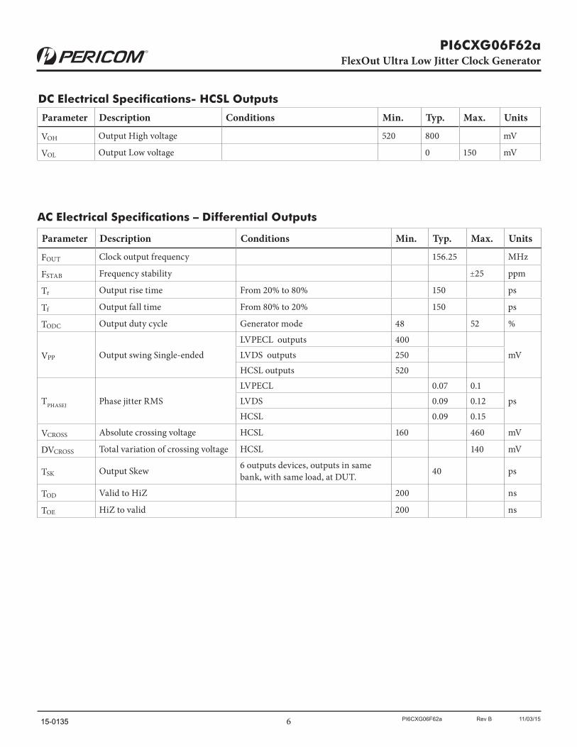
Output Skew
CLK/nCLKTPLHx
VOH
VOL
QAn/QBn
Output Skew T
QAn+1/QBn+1
TPLHy
TSK
TPHLy
TSK
TPHLxVOH
VOL
VOH
VOL
TSK = TPLHy - TPLHx or TSK = TPHLy - TPHLx
SK
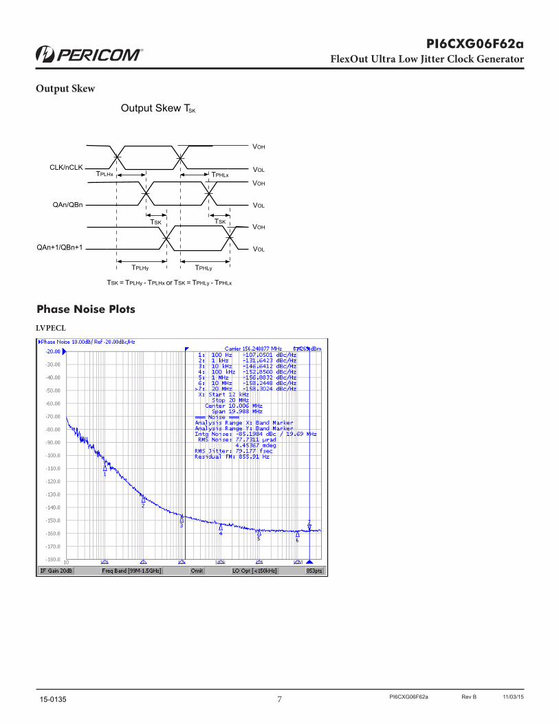
Phase Noise Plots
LVPECL
15-0135
8 PI6CXG06F62a Rev B 11/03/15
PI6CXG06F62a FlexOut Ultra Low Jitter Clock Generator
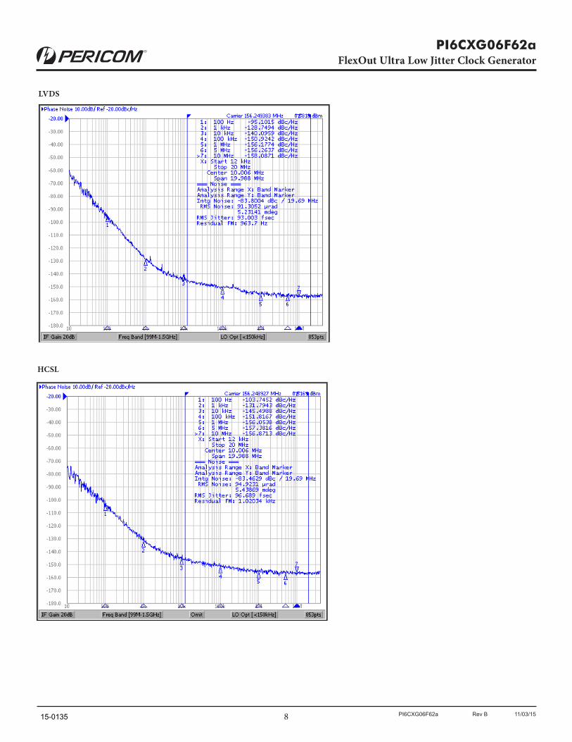
LVDS
HCSL
15-0135
9 PI6CXG06F62a Rev B 11/03/15
PI6CXG06F62a FlexOut Ultra Low Jitter Clock Generator
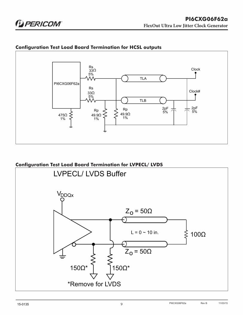
Configuration Test Load Board Termination for HCSL outputs
Rs335%
Rs33Ω5%
Rp49.9Ω
1%475Ω1%
Rp49.9Ω
1%
2pF5%
2pF5%
Clock#
Clock
TLA
TLB
PI6CXG06F62a
Ω
Configuration Test Load Board Termination for LVPECL/ LVDS
100Ω
Z = 50Ωo
Z = 50Ωo
150Ω*150Ω*
LVPECL/ LVDS Buffer
VDDQx
L = 0 ~ 10 in.
*Remove for LVDS
15-0135
10 PI6CXG06F62a Rev B 11/03/15
PI6CXG06F62a FlexOut Ultra Low Jitter Clock Generator
Application information
Suggest for Unused Inputs and OutputsLVCMOS Input Control PinsIt is suggested to add pull-up=4.7k and pull-down=1k for LVC-MOS pins even though they have internal pull-up/down but with much higher value (>=50k) for higher design reliability.
OutputsAll unused outputs are suggested to be left open and not con-nected to any trace. This can lower the IC power supply power.
Power Decoupling & RoutingVDD Pin DecouplingAs general design rule, each VDD pin must have a 0.1uF decou-pling capacitor. For better decoupling, 1uF can be used. Locat-ing the decoupling capacitor on the component side has better decoupling filter result as below.
Placement of Decoupling caps
Clock IC Device
VDD
GND
VDD0.1uF
0.1uFGND
GND
VDD
VDD
Decouple cap. on comp. side
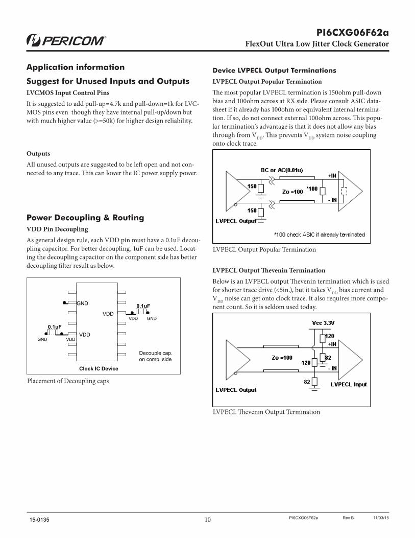
Device LVPECL Output Terminations
LVPECL Output Popular Termination The most popular LVPECL termination is 150ohm pull-down bias and 100ohm across at RX side. Please consult ASIC data-sheet if it already has 100ohm or equivalent internal termina-tion. If so, do not connect external 100ohm across. This popu-lar termination’s advantage is that it does not allow any bias through from VDD. This prevents VDD system noise coupling onto clock trace.
LVPECL Output Thevenin TerminationBelow is an LVPECL output Thevenin termination which is used for shorter trace drive (<5in.), but it takes VDD bias current and VDD noise can get onto clock trace. It also requires more compo-nent count. So it is seldom used today.
LVPECL Output Popular Termination
LVPECL Thevenin Output Termination
15-0135
11 PI6CXG06F62a Rev B 11/03/15
PI6CXG06F62a FlexOut Ultra Low Jitter Clock Generator
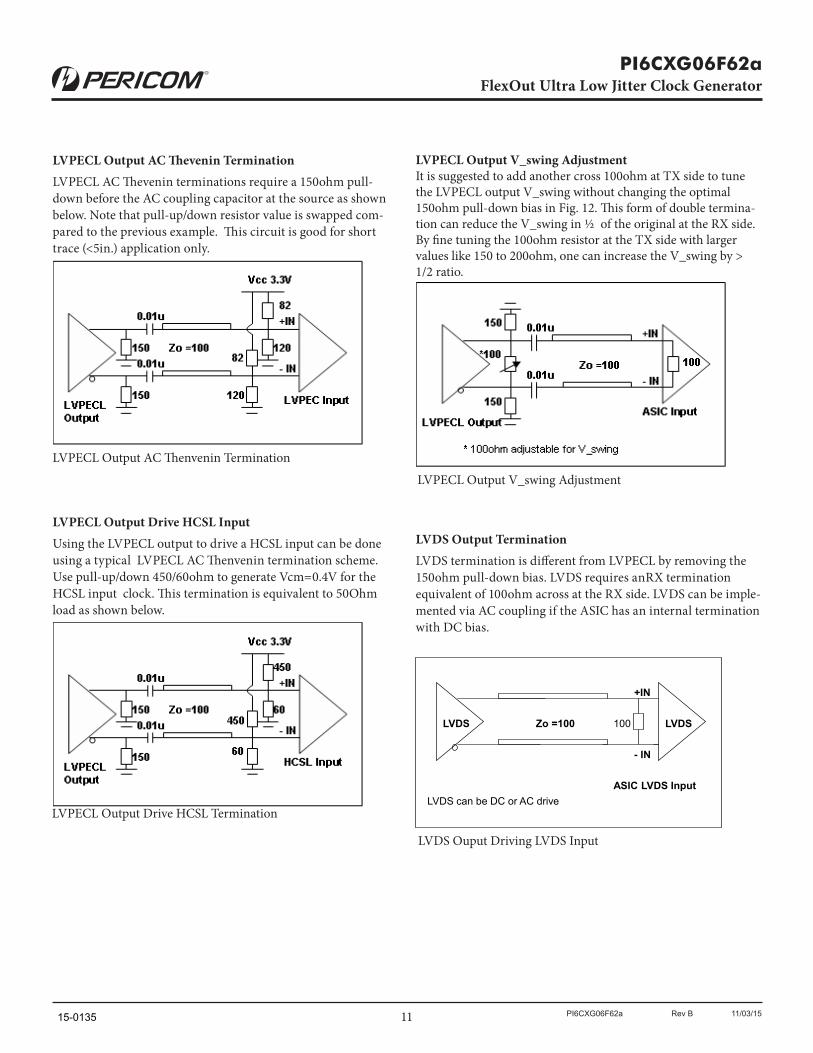
LVPECL Output AC Thevenin Termination LVPECL AC Thevenin terminations require a 150ohm pull-down before the AC coupling capacitor at the source as shown below. Note that pull-up/down resistor value is swapped com-pared to the previous example. This circuit is good for short trace (<5in.) application only.
LVPECL Output Drive HCSL Input Using the LVPECL output to drive a HCSL input can be done using a typical LVPECL AC Thenvenin termination scheme. Use pull-up/down 450/60ohm to generate Vcm=0.4V for the HCSL input clock. This termination is equivalent to 50Ohm load as shown below.
LVPECL Output Drive HCSL Termination
LVPECL Output AC Thenvenin Termination
LVPECL Output V_swing Adjustment It is suggested to add another cross 100ohm at TX side to tune the LVPECL output V_swing without changing the optimal 150ohm pull-down bias in Fig. 12. This form of double termina-tion can reduce the V_swing in ½ of the original at the RX side. By fine tuning the 100ohm resistor at the TX side with larger values like 150 to 200ohm, one can increase the V_swing by > 1/2 ratio.
LVPECL Output V_swing Adjustment
LVDS Output Termination LVDS termination is different from LVPECL by removing the 150ohm pull-down bias. LVDS requires anRX termination equivalent of 100ohm across at the RX side. LVDS can be imple-mented via AC coupling if the ASIC has an internal termination with DC bias.
ASIC LVDS Input
Zo =100LVDS
+IN
- IN
100
LVDS can be DC or AC drive
LVDS
LVDS Ouput Driving LVDS Input
15-0135
12 PI6CXG06F62a Rev B 11/03/15
PI6CXG06F62a FlexOut Ultra Low Jitter Clock Generator
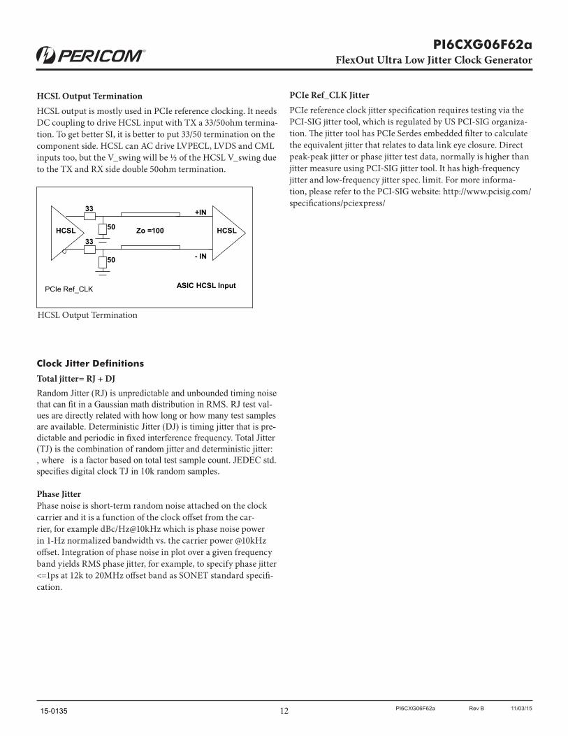
HCSL Output Termination HCSL output is mostly used in PCIe reference clocking. It needs DC coupling to drive HCSL input with TX a 33/50ohm termina-tion. To get better SI, it is better to put 33/50 termination on the component side. HCSL can AC drive LVPECL, LVDS and CML inputs too, but the V_swing will be ½ of the HCSL V_swing due to the TX and RX side double 50ohm termination.
Zo =100
33
33HCSL
PCIe Ref_CLK
50
50
+IN
- IN
HCSL
ASIC HCSL Input
Clock Jitter Definitions
Total jitter= RJ + DJRandom Jitter (RJ) is unpredictable and unbounded timing noise that can fit in a Gaussian math distribution in RMS. RJ test val-ues are directly related with how long or how many test samples are available. Deterministic Jitter (DJ) is timing jitter that is pre-dictable and periodic in fixed interference frequency. Total Jitter (TJ) is the combination of random jitter and deterministic jitter: , where is a factor based on total test sample count. JEDEC std. specifies digital clock TJ in 10k random samples.
Phase JitterPhase noise is short-term random noise attached on the clock carrier and it is a function of the clock offset from the car-rier, for example dBc/Hz@10kHz which is phase noise power in 1-Hz normalized bandwidth vs. the carrier power @10kHz offset. Integration of phase noise in plot over a given frequency band yields RMS phase jitter, for example, to specify phase jitter <=1ps at 12k to 20MHz offset band as SONET standard specifi-cation.
HCSL Output Termination
PCIe Ref_CLK JitterPCIe reference clock jitter specification requires testing via the PCI-SIG jitter tool, which is regulated by US PCI-SIG organiza-tion. The jitter tool has PCIe Serdes embedded filter to calculate the equivalent jitter that relates to data link eye closure. Direct peak-peak jitter or phase jitter test data, normally is higher than jitter measure using PCI-SIG jitter tool. It has high-frequency jitter and low-frequency jitter spec. limit. For more informa-tion, please refer to the PCI-SIG website: http://www.pcisig.com/specifications/pciexpress/
15-0135
13 PI6CXG06F62a Rev B 11/03/15
PI6CXG06F62a FlexOut Ultra Low Jitter Clock Generator
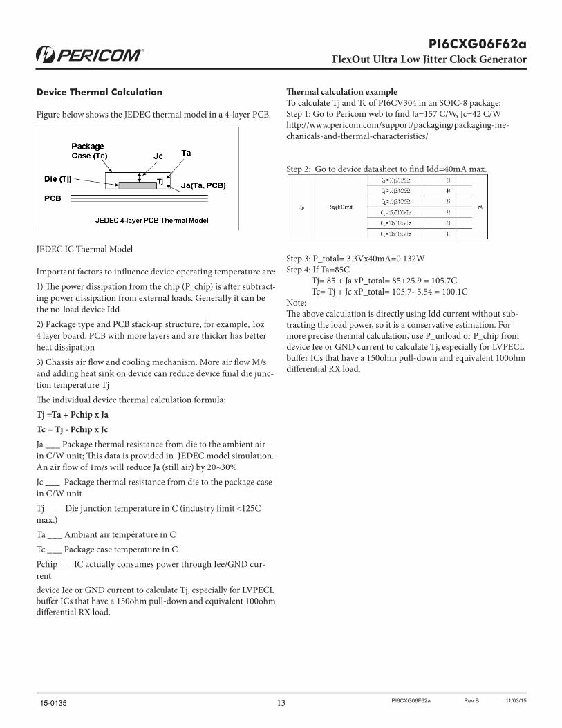
Device Thermal Calculation
Figure below shows the JEDEC thermal model in a 4-layer PCB.
JEDEC IC Thermal Model
Important factors to influence device operating temperature are:1) The power dissipation from the chip (P_chip) is after subtract-ing power dissipation from external loads. Generally it can be the no-load device Idd 2) Package type and PCB stack-up structure, for example, 1oz 4 layer board. PCB with more layers and are thicker has better heat dissipation3) Chassis air flow and cooling mechanism. More air flow M/s and adding heat sink on device can reduce device final die junc-tion temperature TjThe individual device thermal calculation formula:Tj =Ta + Pchip x JaTc = Tj - Pchip x JcJa ___ Package thermal resistance from die to the ambient air in C/W unit; This data is provided in JEDEC model simulation. An air flow of 1m/s will reduce Ja (still air) by 20~30% Jc ___ Package thermal resistance from die to the package case in C/W unitTj ___ Die junction temperature in C (industry limit <125C max.)Ta ___ Ambiant air température in C Tc ___ Package case temperature in C Pchip___ IC actually consumes power through Iee/GND cur-rentdevice Iee or GND current to calculate Tj, especially for LVPECL buffer ICs that have a 150ohm pull-down and equivalent 100ohm differential RX load.
Thermal calculation exampleTo calculate Tj and Tc of PI6CV304 in an SOIC-8 package:Step 1: Go to Pericom web to find Ja=157 C/W, Jc=42 C/Whttp://www.pericom.com/support/packaging/packaging-me-chanicals-and-thermal-characteristics/
Step 2: Go to device datasheet to find Idd=40mA max.
Step 3: P_total= 3.3Vx40mA=0.132WStep 4: If Ta=85C Tj= 85 + Ja xP_total= 85+25.9 = 105.7C Tc= Tj + Jc xP_total= 105.7- 5.54 = 100.1CNote:The above calculation is directly using Idd current without sub-tracting the load power, so it is a conservative estimation. For more precise thermal calculation, use P_unload or P_chip from device Iee or GND current to calculate Tj, especially for LVPECL buffer ICs that have a 150ohm pull-down and equivalent 100ohm differential RX load.
15-0135
14 PI6CXG06F62a Rev B 11/03/15
PI6CXG06F62a FlexOut Ultra Low Jitter Clock Generator
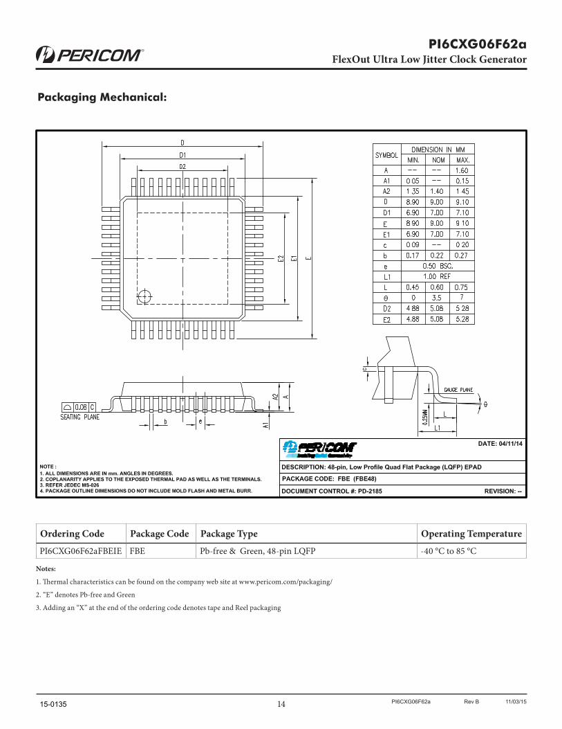
Packaging Mechanical:
Ordering Code Package Code Package Type Operating Temperature
PI6CXG06F62aFBEIE FBE Pb-free & Green, 48-pin LQFP -40 °C to 85 °C
Notes:
1. Thermal characteristics can be found on the company web site at www.pericom.com/packaging/
2. “E” denotes Pb-free and Green
3. Adding an “X” at the end of the ordering code denotes tape and Reel packaging
15-0135