Embed Size (px)
Citation preview
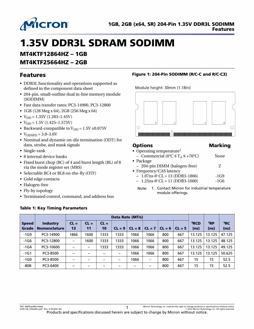
1.35V DDR3L SDRAM SODIMMMT4KTF12864HZ – 1GBMT4KTF25664HZ – 2GB
Features• DDR3L functionality and operations supported as
defined in the component data sheet• 204-pin, small-outline dual in-line memory module
(SODIMM)• Fast data transfer rates: PC3-14900, PC3-12800• 1GB (128 Meg x 64), 2GB (256 Meg x 64)• VDD = 1.35V (1.283–1.45V)• VDD = 1.5V (1.425–1.575V)• Backward-compatible to VDD = 1.5V ±0.075V• VDDSPD = 3.0–3.6V• Nominal and dynamic on-die termination (ODT) for
data, strobe, and mask signals• Single-rank• 8 internal device banks• Fixed burst chop (BC) of 4 and burst length (BL) of 8
via the mode register set (MRS)• Selectable BC4 or BL8 on-the-fly (OTF)• Gold edge contacts• Halogen-free• Fly-by topology• Terminated control, command, and address bus
Figure 1: 204-Pin SODIMM (R/C-C and R/C-C3)
Module height: 30mm (1.18in)
Options Marking• Operating temperature1
– Commercial (0°C ≤ TA ≤ +70°C) None• Package
– 204-pin DIMM (halogen-free) Z• Frequency/CAS latency
– 1.07ns @ CL = 13 (DDR3-1866) -1G9– 1.25ns @ CL = 11 (DDR3-1600) -1G6
Note: 1. Contact Micron for industrial temperaturemodule offerings.
Table 1: Key Timing Parameters
SpeedGrade
IndustryNomenclature
Data Rate (MT/s)tRCD(ns)
tRP(ns)
tRC(ns)
CL =13
CL =11
CL =10 CL = 9 CL = 8 CL = 7 CL = 6 CL = 5
-1G9 PC3-14900 1866 1600 1333 1333 1066 1066 800 667 13.125 13.125 47.125
-1G6 PC3-12800 – 1600 1333 1333 1066 1066 800 667 13.125 13.125 48.125
-1G4 PC3-10600 – – 1333 1333 1066 1066 800 667 13.125 13.125 49.125
-1G1 PC3-8500 – – – – 1066 1066 800 667 13.125 13.125 50.625
-1G0 PC3-8500 – – – – 1066 – 800 667 15 15 52.5
-80B PC3-6400 – – – – – – 800 667 15 15 52.5
1GB, 2GB (x64, SR) 204-Pin 1.35V DDR3L SODIMMFeatures
PDF: 09005aef84c19de9ktf4c128_256x64hz.pdf - Rev. G 05/2021 EN 1 Micron Technology, Inc. reserves the right to change products or specifications without notice.
© 2012 Micron Technology, Inc. All rights reserved.
Products and specifications discussed herein are subject to change by Micron without notice.
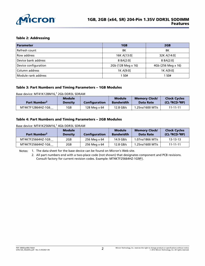
Table 2: Addressing
Parameter 1GB 2GB
Refresh count 8K 8K
Row address 16K A[13:0] 32K A[14:0]
Device bank address 8 BA[2:0] 8 BA[2:0]
Device configuration 2Gb (128 Meg x 16) 4Gb (256 Meg x 16)
Column address 1K A[9:0] 1K A[9:0]
Module rank address 1 S0# 1 S0#
Table 3: Part Numbers and Timing Parameters – 1GB Modules
Base device: MT41K128M16,1 2Gb DDR3L SDRAM
Part Number2ModuleDensity Configuration
ModuleBandwidth
Memory Clock/Data Rate
Clock Cycles(CL-tRCD-tRP)
MT4KTF12864HZ-1G6__ 1GB 128 Meg x 64 12.8 GB/s 1.25ns/1600 MT/s 11-11-11
Table 4: Part Numbers and Timing Parameters – 2GB Modules
Base device: MT41K256M16,1 4Gb DDR3L SDRAM
Part Number2ModuleDensity Configuration
ModuleBandwidth
Memory Clock/Data Rate
Clock Cycles(CL-tRCD-tRP)
MT4KTF25664HZ-1G9__ 2GB 256 Meg x 64 14.9 GB/s 1.07ns/1866 MT/s 13-13-13
MT4KTF25664HZ-1G6__ 2GB 256 Meg x 64 12.8 GB/s 1.25ns/1600 MT/s 11-11-11
Notes: 1. The data sheet for the base device can be found on Micron’s Web site.2. All part numbers end with a two-place code (not shown) that designates component and PCB revisions.
Consult factory for current revision codes. Example: MT4KTF25664HZ-1G9P1.
1GB, 2GB (x64, SR) 204-Pin 1.35V DDR3L SODIMMFeatures
PDF: 09005aef84c19de9ktf4c128_256x64hz.pdf - Rev. G 05/2021 EN 2 Micron Technology, Inc. reserves the right to change products or specifications without notice.
© 2012 Micron Technology, Inc. All rights reserved.
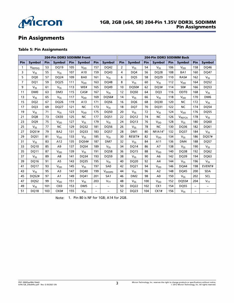
Pin Assignments
Table 5: Pin Assignments
204-Pin DDR3 SODIMM Front 204-Pin DDR3 SODIMM Back
Pin Symbol Pin Symbol Pin Symbol Pin Symbol Pin Symbol Pin Symbol Pin Symbol Pin Symbol
1 VREFDQ 53 DQ19 105 VDD 157 DQ42 2 VSS 54 VSS 106 VDD 158 DQ46
3 VSS 55 VSS 107 A10 159 DQ43 4 DQ4 56 DQ28 108 BA1 160 DQ47
5 DQ0 57 DQ24 109 BA0 161 VSS 6 DQ5 58 DQ29 110 RAS# 162 VSS
7 DQ1 59 DQ25 111 VDD 163 DQ48 8 VSS 60 VSS 112 VDD 164 DQ52
9 VSS 61 VSS 113 WE# 165 DQ49 10 DQS0# 62 DQ3# 114 S0# 166 DQ53
11 DM0 63 DM3 115 CAS# 167 VSS 12 DQS0 64 DQ3 116 ODT0 168 VSS
13 VSS 65 VSS 117 VDD 169 DQS6# 14 VSS 66 VSS 118 VDD 170 DM6
15 DQ2 67 DQ26 119 A13 171 DQS6 16 DQ6 68 DQ30 120 NC 172 VSS
17 DQ3 69 DQ27 121 NC 173 VSS 18 DQ7 70 DQ31 122 NC 174 DQ54
19 VSS 71 VSS 123 VDD 175 DQ50 20 VSS 72 VSS 124 VDD 176 DQ55
21 DQ8 73 CKE0 125 NC 177 DQ51 22 DQ12 74 NC 126 VREFCA 178 VSS
23 DQ9 75 VDD 127 VSS 179 VSS 24 DQ13 76 VDD 128 VSS 180 DQ60
25 VSS 77 NC 129 DQ32 181 DQ56 26 VSS 78 NC 130 DQ36 182 DQ61
27 DQS1# 79 BA2 131 DQ33 183 DQ57 28 DM1 80 NF/A141 132 DQ37 184 VSS
29 DQS1 81 VDD 133 VSS 185 VSS 30 RESET# 82 VDD 134 VSS 186 DQS7#
31 VSS 83 A12 135 DQS4# 187 DM7 32 VSS 84 A11 136 DM4 188 DQS7
33 DQ10 85 A9 137 DQS4 189 VSS 34 DQ14 86 A7 138 VSS 190 VSS
35 DQ11 87 VDD 139 VSS 191 DQ58 36 DQ15 88 VDD 140 DQ38 192 DQ62
37 VSS 89 A8 141 DQ34 193 DQ59 38 VSS 90 A6 142 DQ39 194 DQ63
39 DQ16 91 A5 143 DQ35 195 VSS 40 DQ20 92 A4 144 VSS 196 VSS
41 DQ17 93 VDD 145 VSS 197 SA0 42 DQ21 94 VDD 146 DQ44 198 EVENT#
43 VSS 95 A3 147 DQ40 199 VDDSPD 44 VSS 96 A2 148 DQ45 200 SDA
45 DQS2# 97 A1 149 DQ41 201 SA1 46 DM2 98 A0 150 VSS 202 SCL
47 DQS2 99 VDD 151 VSS 203 VTT 48 VSS 100 VDD 152 DQS5# 204 VTT
49 VSS 101 CK0 153 DM5 – – 50 DQ22 102 CK1 154 DQS5 – –
51 DQ18 103 CK0# 155 VSS – – 52 DQ23 104 CK1# 156 VSS – –
Note: 1. Pin 80 is NF for 1GB; A14 for 2GB.
1GB, 2GB (x64, SR) 204-Pin 1.35V DDR3L SODIMMPin Assignments
PDF: 09005aef84c19de9ktf4c128_256x64hz.pdf - Rev. G 05/2021 EN 3 Micron Technology, Inc. reserves the right to change products or specifications without notice.
© 2012 Micron Technology, Inc. All rights reserved.
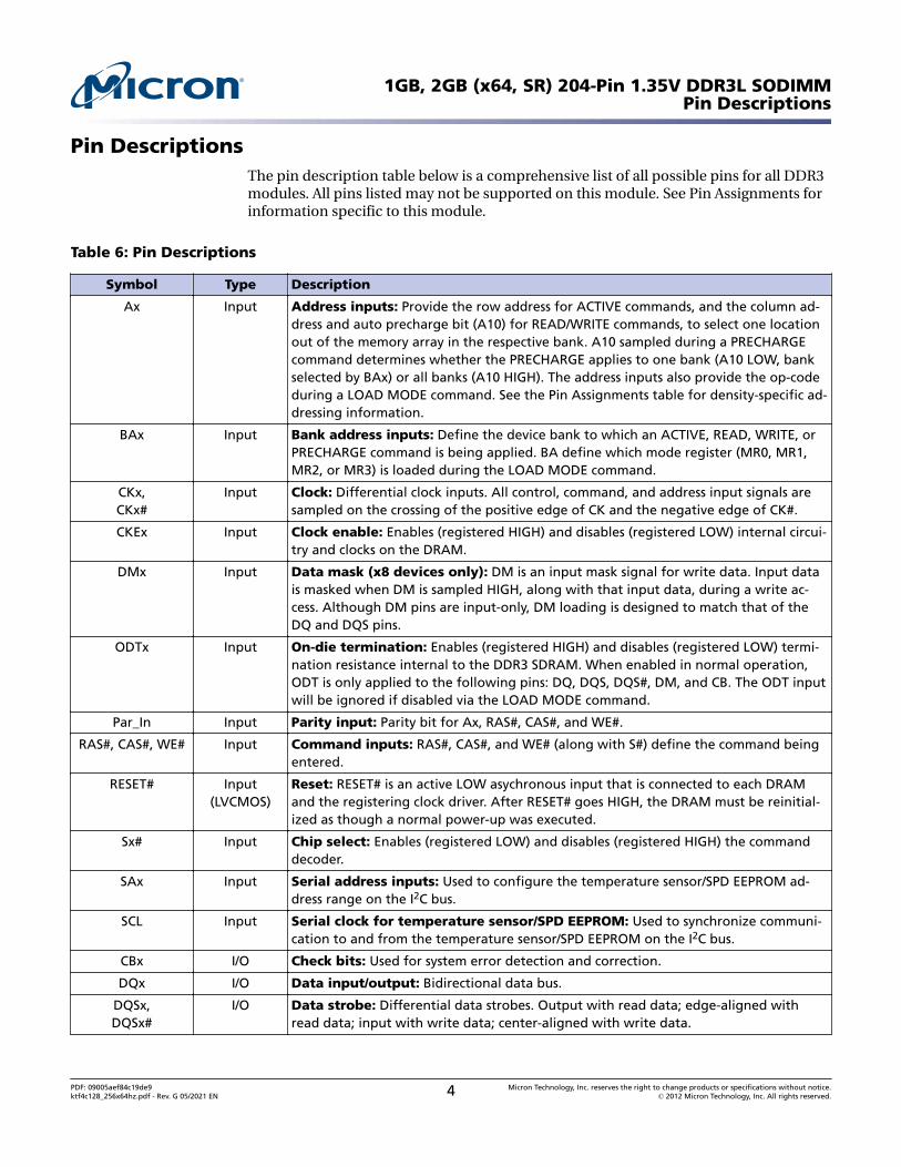
Pin DescriptionsThe pin description table below is a comprehensive list of all possible pins for all DDR3modules. All pins listed may not be supported on this module. See Pin Assignments forinformation specific to this module.
Table 6: Pin Descriptions
Symbol Type Description
Ax Input Address inputs: Provide the row address for ACTIVE commands, and the column ad-dress and auto precharge bit (A10) for READ/WRITE commands, to select one locationout of the memory array in the respective bank. A10 sampled during a PRECHARGEcommand determines whether the PRECHARGE applies to one bank (A10 LOW, bankselected by BAx) or all banks (A10 HIGH). The address inputs also provide the op-codeduring a LOAD MODE command. See the Pin Assignments table for density-specific ad-dressing information.
BAx Input Bank address inputs: Define the device bank to which an ACTIVE, READ, WRITE, orPRECHARGE command is being applied. BA define which mode register (MR0, MR1,MR2, or MR3) is loaded during the LOAD MODE command.
CKx,CKx#
Input Clock: Differential clock inputs. All control, command, and address input signals aresampled on the crossing of the positive edge of CK and the negative edge of CK#.
CKEx Input Clock enable: Enables (registered HIGH) and disables (registered LOW) internal circui-try and clocks on the DRAM.
DMx Input Data mask (x8 devices only): DM is an input mask signal for write data. Input datais masked when DM is sampled HIGH, along with that input data, during a write ac-cess. Although DM pins are input-only, DM loading is designed to match that of theDQ and DQS pins.
ODTx Input On-die termination: Enables (registered HIGH) and disables (registered LOW) termi-nation resistance internal to the DDR3 SDRAM. When enabled in normal operation,ODT is only applied to the following pins: DQ, DQS, DQS#, DM, and CB. The ODT inputwill be ignored if disabled via the LOAD MODE command.
Par_In Input Parity input: Parity bit for Ax, RAS#, CAS#, and WE#.
RAS#, CAS#, WE# Input Command inputs: RAS#, CAS#, and WE# (along with S#) define the command beingentered.
RESET# Input(LVCMOS)
Reset: RESET# is an active LOW asychronous input that is connected to each DRAMand the registering clock driver. After RESET# goes HIGH, the DRAM must be reinitial-ized as though a normal power-up was executed.
Sx# Input Chip select: Enables (registered LOW) and disables (registered HIGH) the commanddecoder.
SAx Input Serial address inputs: Used to configure the temperature sensor/SPD EEPROM ad-dress range on the I2C bus.
SCL Input Serial clock for temperature sensor/SPD EEPROM: Used to synchronize communi-cation to and from the temperature sensor/SPD EEPROM on the I2C bus.
CBx I/O Check bits: Used for system error detection and correction.
DQx I/O Data input/output: Bidirectional data bus.
DQSx,DQSx#
I/O Data strobe: Differential data strobes. Output with read data; edge-aligned withread data; input with write data; center-aligned with write data.
1GB, 2GB (x64, SR) 204-Pin 1.35V DDR3L SODIMMPin Descriptions
PDF: 09005aef84c19de9ktf4c128_256x64hz.pdf - Rev. G 05/2021 EN 4 Micron Technology, Inc. reserves the right to change products or specifications without notice.
© 2012 Micron Technology, Inc. All rights reserved.

Table 6: Pin Descriptions (Continued)
Symbol Type Description
SDA I/O Serial data: Used to transfer addresses and data into and out of the temperature sen-sor/SPD EEPROM on the I2C bus.
TDQSx,TDQSx#
Output Redundant data strobe (x8 devices only): TDQS is enabled/disabled via the LOADMODE command to the extended mode register (EMR). When TDQS is enabled, DM isdisabled and TDQS and TDQS# provide termination resistance; otherwise, TDQS# areno function.
Err_Out# Output(open drain)
Parity error output: Parity error found on the command and address bus.
EVENT# Output(open drain)
Temperature event: The EVENT# pin is asserted by the temperature sensor when crit-ical temperature thresholds have been exceeded.
VDD Supply Power supply: 1.35V (1.283–1.45V) backward-compatible to 1.5V (1.425–1.575V). Thecomponent VDD and VDDQ are connected to the module VDD.
VDDSPD Supply Temperature sensor/SPD EEPROM power supply: 3.0–3.6V.
VREFCA Supply Reference voltage: Control, command, and address VDD/2.
VREFDQ Supply Reference voltage: DQ, DM VDD/2.
VSS Supply Ground.
VTT Supply Termination voltage: Used for control, command, and address VDD/2.
NC – No connect: These pins are not connected on the module.
NF – No function: These pins are connected within the module, but provide no functional-ity.
1GB, 2GB (x64, SR) 204-Pin 1.35V DDR3L SODIMMPin Descriptions
PDF: 09005aef84c19de9ktf4c128_256x64hz.pdf - Rev. G 05/2021 EN 5 Micron Technology, Inc. reserves the right to change products or specifications without notice.
© 2012 Micron Technology, Inc. All rights reserved.
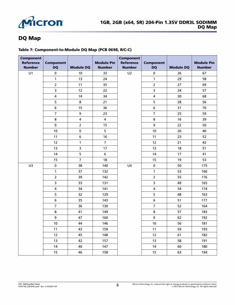
DQ Map
Table 7: Component-to-Module DQ Map (PCB 0698, R/C-C)
ComponentReferenceNumber
ComponentDQ Module DQ
Module PinNumber
ComponentReferenceNumber
ComponentDQ Module DQ
Module PinNumber
U1 0 10 33 U2 0 26 67
1 13 24 1 29 58
2 11 35 2 27 69
3 12 22 3 24 57
4 14 34 4 30 68
5 8 21 5 28 56
6 15 36 6 31 70
7 9 23 7 25 59
8 4 4 8 16 39
9 2 15 9 22 50
10 0 5 10 20 40
11 6 16 11 23 52
12 1 7 12 21 42
13 3 17 13 18 51
14 5 6 14 17 41
15 7 18 15 19 53
U3 0 38 140 U4 0 50 175
1 37 132 1 53 166
2 39 142 2 55 176
3 33 131 3 49 165
4 34 141 4 54 174
5 32 129 5 48 163
6 35 143 6 51 177
7 36 130 7 52 164
8 41 149 8 57 183
9 47 160 9 62 192
10 44 146 10 56 181
11 43 159 11 59 193
12 45 148 12 61 182
13 42 157 13 58 191
14 40 147 14 60 180
15 46 158 15 63 194
1GB, 2GB (x64, SR) 204-Pin 1.35V DDR3L SODIMMDQ Map
PDF: 09005aef84c19de9ktf4c128_256x64hz.pdf - Rev. G 05/2021 EN 6 Micron Technology, Inc. reserves the right to change products or specifications without notice.
© 2012 Micron Technology, Inc. All rights reserved.
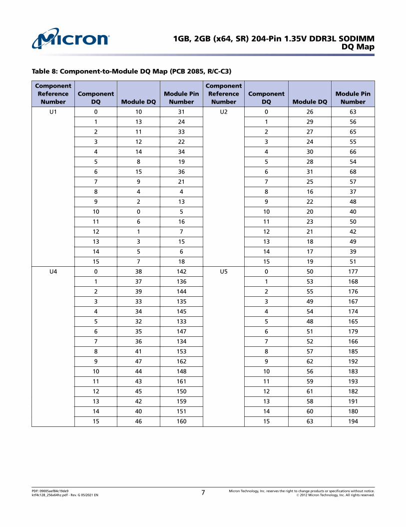
Table 8: Component-to-Module DQ Map (PCB 2085, R/C-C3)
ComponentReferenceNumber
ComponentDQ Module DQ
Module PinNumber
ComponentReferenceNumber
ComponentDQ Module DQ
Module PinNumber
U1 0 10 31 U2 0 26 63
1 13 24 1 29 56
2 11 33 2 27 65
3 12 22 3 24 55
4 14 34 4 30 66
5 8 19 5 28 54
6 15 36 6 31 68
7 9 21 7 25 57
8 4 4 8 16 37
9 2 13 9 22 48
10 0 5 10 20 40
11 6 16 11 23 50
12 1 7 12 21 42
13 3 15 13 18 49
14 5 6 14 17 39
15 7 18 15 19 51
U4 0 38 142 U5 0 50 177
1 37 136 1 53 168
2 39 144 2 55 176
3 33 135 3 49 167
4 34 145 4 54 174
5 32 133 5 48 165
6 35 147 6 51 179
7 36 134 7 52 166
8 41 153 8 57 185
9 47 162 9 62 192
10 44 148 10 56 183
11 43 161 11 59 193
12 45 150 12 61 182
13 42 159 13 58 191
14 40 151 14 60 180
15 46 160 15 63 194
1GB, 2GB (x64, SR) 204-Pin 1.35V DDR3L SODIMMDQ Map
PDF: 09005aef84c19de9ktf4c128_256x64hz.pdf - Rev. G 05/2021 EN 7 Micron Technology, Inc. reserves the right to change products or specifications without notice.
© 2012 Micron Technology, Inc. All rights reserved.

Functional Block Diagram
Figure 2: Functional Block Diagram (PCB 0698, R/C-C)
DQS# DQS DMDQDQ DQ DQ DQ DQDQDQDQS#DQS DMDQ DQDQDQ DQ DQ DQDQZQ
DQ0 DQ1 DQ2 DQ3 DQ4 DQ5 DQ6 DQ7
DQ8 DQ9 DQ10 DQ11 DQ12 DQ13 DQ14 DQ15
DQ32 DQ33 DQ34 DQ35 DQ36 DQ37 DQ38 DQ39
DQ40 DQ41 DQ42 DQ43 DQ44 DQ45 DQ46 DQ47
DQ16 DQ17 DQ18 DQ19 DQ20 DQ21 DQ22 DQ23
DQ24 DQ25 DQ26 DQ27 DQ28 DQ29 DQ30 DQ31
DQ48 DQ49 DQ50 DQ51 DQ52 DQ53 DQ54 DQ55
DQ56 DQ57 DQ58 DQ59 DQ60 DQ61 DQ62 DQ63
DQS1# DQS1 DM1
DQS2# DQS2 DM2
DQS3# DQS3 DM3
DQS4# DQS4 DM4
DQS5# DQS5 DM5
DQS6# DQS6 DM6
DQS7# DQS7 DM7
CS#
CS# CS#
CS#
U1
U2
U3
U4
S0#
DQS# DQS DMDQDQ DQ DQ DQ DQDQDQDQS#DQS DMDQ DQDQDQ DQ DQ DQDQZQ
DQS# DQS DMDQDQ DQ DQ DQ DQDQDQDQS#DQS DMDQ DQDQDQ DQ DQ DQDQZQ
DQS# DQS DMDQDQ DQ DQ DQ DQDQDQDQS#DQS DMDQ DQDQDQ DQ DQ DQDQZQ
BA[2:0]A[14/13:0]
RAS#
CAS#
WE#
CKE0
ODT0
RESET#
BA[2:0]: DDR3 SDRAM
RAS#: DDR3 SDRAM
CAS#: DDR3 SDRAM
WE#: DDR3 SDRAM
CKE0: DDR3 SDRAM
ODT0: DDR3 SDRAM
RESET#: DDR3 SDRAM
DDR3 SDRAM x4CK0
CK0#
CK1CK1#
VREFCA
VSS
DDR3 SDRAM
DDR3 SDRAM
VDD
Control, command, and address termination
VDDSPD
VTT
DDR3 SDRAM
DDR3 SDRAMVREFDQ
Clock, control, command, and address line terminations:
DQS0# DQS0 DM0
U8
VSS
VSSVSS
VSS
A0
SPD EEPROM
A1 A2
SA0 SA1
SDASCLWP
VSS
CKE0, A[14/13:0], RAS#, CAS#, WE#,
ODT0, BA[2:0], S0#
DDR3 SDRAM
VTT
CK CK#
DDR3 SDRAM
VDD
SPD EEPROM
VSS
A[14/13:0]: DDR3 SDRAM
Note: 1. The ZQ ball on each DDR3 component is connected to an external 240Ω ±1% resistorthat is tied to ground. It is used for the calibration of the component’s ODT and outputdriver.
1GB, 2GB (x64, SR) 204-Pin 1.35V DDR3L SODIMMFunctional Block Diagram
PDF: 09005aef84c19de9ktf4c128_256x64hz.pdf - Rev. G 05/2021 EN 8 Micron Technology, Inc. reserves the right to change products or specifications without notice.
© 2012 Micron Technology, Inc. All rights reserved.
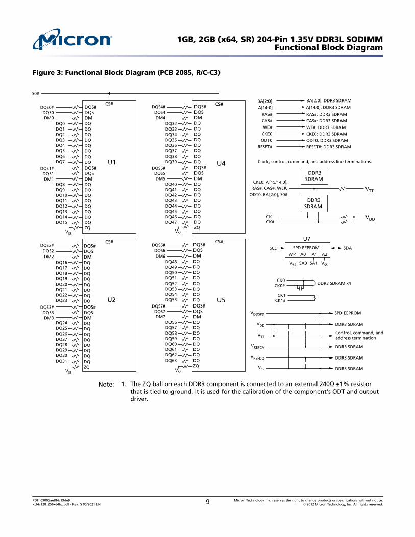
Figure 3: Functional Block Diagram (PCB 2085, R/C-C3)
DQS# DQS DMDQDQ DQ DQ DQ DQDQDQDQS#DQS DMDQ DQDQDQ DQ DQ DQDQZQ
DQ0 DQ1 DQ2 DQ3 DQ4 DQ5 DQ6 DQ7
DQ8 DQ9 DQ10 DQ11 DQ12 DQ13 DQ14 DQ15
DQ32 DQ33 DQ34 DQ35 DQ36 DQ37 DQ38 DQ39
DQ40 DQ41 DQ42 DQ43 DQ44 DQ45 DQ46 DQ47
DQ16 DQ17 DQ18 DQ19 DQ20 DQ21 DQ22 DQ23
DQ24 DQ25 DQ26 DQ27 DQ28 DQ29 DQ30 DQ31
DQ48 DQ49 DQ50 DQ51 DQ52 DQ53 DQ54 DQ55
DQ56 DQ57 DQ58 DQ59 DQ60 DQ61 DQ62 DQ63
DQS1# DQS1 DM1
DQS2# DQS2 DM2
DQS3# DQS3 DM3
DQS4# DQS4 DM4
DQS5# DQS5 DM5
DQS6# DQS6 DM6
DQS7# DQS7 DM7
CS#
CS# CS#
CS#
U1
U2
U4
U5
S0#
DQS# DQS DMDQDQ DQ DQ DQ DQDQDQDQS#DQS DMDQ DQDQDQ DQ DQ DQDQZQ
DQS# DQS DMDQDQ DQ DQ DQ DQDQDQDQS#DQS DMDQ DQDQDQ DQ DQ DQDQZQ
DQS# DQS DMDQDQ DQ DQ DQ DQDQDQDQS#DQS DMDQ DQDQDQ DQ DQ DQDQZQ
BA[2:0] A[14:0]
RAS#
CAS#
WE#
CKE0
ODT0
RESET#
BA[2:0]: DDR3 SDRAM
RAS#: DDR3 SDRAM
CAS#: DDR3 SDRAM
WE#: DDR3 SDRAM
CKE0: DDR3 SDRAM
ODT0: DDR3 SDRAM
RESET#: DDR3 SDRAM
DDR3 SDRAM x4CK0
CK0#
CK1CK1#
VREFCA
VSS
DDR3 SDRAM
DDR3 SDRAM
VDD
Control, command, and address termination
VDDSPD
VTT
DDR3 SDRAM
DDR3 SDRAMVREFDQ
Clock, control, command, and address line terminations:
DQS0# DQS0 DM0
U7
VSS
VSSVSS
VSS
A0
SPD EEPROM
A1 A2
SA0 SA1
SDASCLWP
VSS
CKE0, A[15/14:0], RAS#, CAS#, WE#,
ODT0, BA[2:0], S0#
DDR3 SDRAM
VTT
CK CK#
DDR3 SDRAM
VDD
SPD EEPROM
VSS
A[14:0]: DDR3 SDRAM
Note: 1. The ZQ ball on each DDR3 component is connected to an external 240Ω ±1% resistorthat is tied to ground. It is used for the calibration of the component’s ODT and outputdriver.
1GB, 2GB (x64, SR) 204-Pin 1.35V DDR3L SODIMMFunctional Block Diagram
PDF: 09005aef84c19de9ktf4c128_256x64hz.pdf - Rev. G 05/2021 EN 9 Micron Technology, Inc. reserves the right to change products or specifications without notice.
© 2012 Micron Technology, Inc. All rights reserved.
General DescriptionDDR3 SDRAM modules are high-speed, CMOS dynamic random access memory mod-ules that use internally configured 8-bank DDR3 SDRAM devices. DDR3 SDRAM mod-ules use DDR architecture to achieve high-speed operation. DDR3 architecture is essen-tially an 8n-prefetch architecture with an interface designed to transfer two data wordsper clock cycle at the I/O pins. A single read or write access for the DDR3 SDRAM mod-ule effectively consists of a single 8n-bit-wide, one-clock-cycle data transfer at the inter-nal DRAM core and eight corresponding n-bit-wide, one-half-clock-cycle data transfersat the I/O pins.
DDR3 modules use two sets of differential signals: DQS, DQS# to capture data and CKand CK# to capture commands, addresses, and control signals. Differential clocks anddata strobes ensure exceptional noise immunity for these signals and provide precisecrossing points to capture input signals.
Fly-By Topology
DDR3 modules use faster clock speeds than earlier DDR technologies, making signalquality more important than ever. For improved signal quality, the clock, control, com-mand, and address buses have been routed in a fly-by topology, where each clock, con-trol, command, and address pin on each DRAM is connected to a single trace and ter-minated (rather than a tree structure, where the termination is off the module near theconnector). Inherent to fly-by topology, the timing skew between the clock and DQS sig-nals can be easily accounted for by using the write-leveling feature of DDR3.
Serial Presence-Detect EEPROM OperationDDR3 SDRAM modules incorporate serial presence-detect. The SPD data is stored in a256-byte EEPROM. The first 128 bytes are programmed by Micron to comply withJEDEC standard JC-45, "Appendix X: Serial Presence Detect (SPD) for DDR3 SDRAMModules." These bytes identify module-specific timing parameters, configuration infor-mation, and physical attributes. The remaining 128 bytes of storage are available for useby the customer. System READ/WRITE operations between the master (system logic)and the slave EEPROM device occur via a standard I2C bus using the DIMM’s SCL(clock) SDA (data), and SA (address) pins. Write protect (WP) is connected to V SS, per-manently disabling hardware write protection. For further information refer to Microntechnical note TN-04-42, "Memory Module Serial Presence-Detect."
1GB, 2GB (x64, SR) 204-Pin 1.35V DDR3L SODIMMGeneral Description
PDF: 09005aef84c19de9ktf4c128_256x64hz.pdf - Rev. G 05/2021 EN 10 Micron Technology, Inc. reserves the right to change products or specifications without notice.
© 2012 Micron Technology, Inc. All rights reserved.
Electrical SpecificationsStresses greater than those listed may cause permanent damage to the module. This is astress rating only, and functional operation of the module at these or any other condi-tions outside those indicated in each device's data sheet is not implied. Exposure to ab-solute maximum rating conditions for extended periods may adversely affect reliability.
Table 9: Absolute Maximum Ratings
Symbol Parameter Min Max Units
VDD VDD supply voltage relative to VSS –0.4 1.975 V
VIN, VOUT Voltage on any pin relative to VSS –0.4 1.975 V
Table 10: Operating Conditions
Symbol Parameter Min Nom Max Units Notes
VDD VDD supply voltage 1.283 1.35 1.45 V
1.425 1.5 1.575 V 1
VREFCA(DC) Input reference voltage command/address bus 0.49 x VDD 0.5 x VDD 0.51 x VDD V
VREFDQ(DC) I/O reference voltage DQ bus 0.49 x VDD 0.5 x VDD 0.51 x VDD V
IVTT Termination reference current from VTT –600 – 600 mA
VTT Termination reference voltage (DC) – command/address bus
0.49 × VDD -20mV
0.5 × VDD 0.51 × VDD +20mV
V 2
II Input leakage current; Any input0V ≤ VIN ≤ VDD; VREF input 0V ≤ VIN
≤ 0.95V (All other pins not undertest = 0V)
Address inputs,RAS#, CAS#,WE#, S#, CKE,ODT, BA, CK,CK#
–8 0 8 µA
DM –2 0 2
IOZ Output leakage current; 0V ≤ VOUT
≤ VDDQ; DQ and ODT are disabled;ODT is HIGH
DQ, DQS, DQS# –5 0 5 µA
IVREF VREF supply leakage current; VREFDQ = VDD/2 or VREF-
CA = VDD/2 (All other pins not under test = 0V)–4 0 4 µA
TA Module ambient operating tem-perature
Commercial 0 – 70 °C 3, 4
TC DDR3 SDRAM component case op-erating temperature
Commercial 0 – 95 °C 3, 4, 5
Notes: 1. Module is backward-compatible with 1.5V operation. Refer to device specification fordetails and operation guidance.
2. VTT termination voltage in excess of the stated limit will adversely affect the commandand address signals’ voltage margin and will reduce timing margins.
3. TA and TC are simultaneous requirements.4. For further information, refer to technical note TN-00-08: “Thermal Applications,” avail-
able on Micron’s Web site.5. The refresh rate is required to double when 85°C < TC ≤ 95°C.
1GB, 2GB (x64, SR) 204-Pin 1.35V DDR3L SODIMMElectrical Specifications
PDF: 09005aef84c19de9ktf4c128_256x64hz.pdf - Rev. G 05/2021 EN 11 Micron Technology, Inc. reserves the right to change products or specifications without notice.
© 2012 Micron Technology, Inc. All rights reserved.
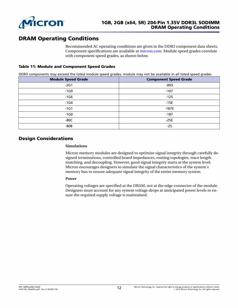
DRAM Operating ConditionsRecommended AC operating conditions are given in the DDR3 component data sheets.Component specifications are available at micron.com. Module speed grades correlatewith component speed grades, as shown below.
Table 11: Module and Component Speed Grades
DDR3 components may exceed the listed module speed grades; module may not be available in all listed speed gradesModule Speed Grade Component Speed Grade
-2G1 -093
-1G9 -107
-1G6 -125
-1G4 -15E
-1G1 -187E
-1G0 -187
-80C -25E
-80B -25
Design Considerations
Simulations
Micron memory modules are designed to optimize signal integrity through carefully de-signed terminations, controlled board impedances, routing topologies, trace lengthmatching, and decoupling. However, good signal integrity starts at the system level.Micron encourages designers to simulate the signal characteristics of the system'smemory bus to ensure adequate signal integrity of the entire memory system.
Power
Operating voltages are specified at the DRAM, not at the edge connector of the module.Designers must account for any system voltage drops at anticipated power levels to en-sure the required supply voltage is maintained.
1GB, 2GB (x64, SR) 204-Pin 1.35V DDR3L SODIMMDRAM Operating Conditions
PDF: 09005aef84c19de9ktf4c128_256x64hz.pdf - Rev. G 05/2021 EN 12 Micron Technology, Inc. reserves the right to change products or specifications without notice.
© 2012 Micron Technology, Inc. All rights reserved.
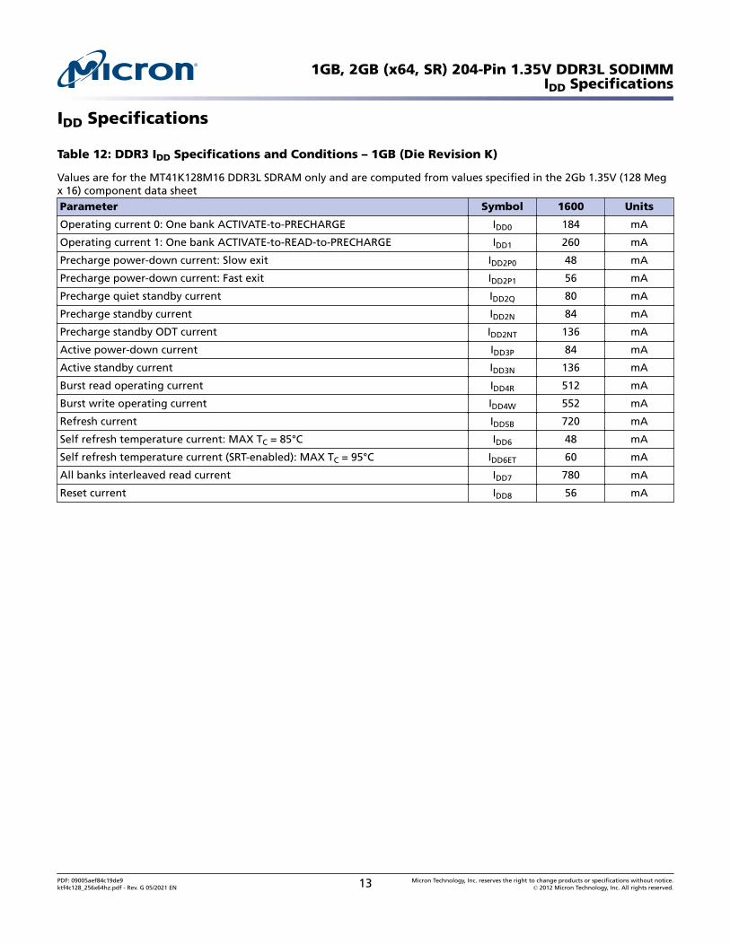
IDD Specifications
Table 12: DDR3 IDD Specifications and Conditions – 1GB (Die Revision K)
Values are for the MT41K128M16 DDR3L SDRAM only and are computed from values specified in the 2Gb 1.35V (128 Megx 16) component data sheetParameter Symbol 1600 Units
Operating current 0: One bank ACTIVATE-to-PRECHARGE IDD0 184 mA
Operating current 1: One bank ACTIVATE-to-READ-to-PRECHARGE IDD1 260 mA
Precharge power-down current: Slow exit IDD2P0 48 mA
Precharge power-down current: Fast exit IDD2P1 56 mA
Precharge quiet standby current IDD2Q 80 mA
Precharge standby current IDD2N 84 mA
Precharge standby ODT current IDD2NT 136 mA
Active power-down current IDD3P 84 mA
Active standby current IDD3N 136 mA
Burst read operating current IDD4R 512 mA
Burst write operating current IDD4W 552 mA
Refresh current IDD5B 720 mA
Self refresh temperature current: MAX TC = 85°C IDD6 48 mA
Self refresh temperature current (SRT-enabled): MAX TC = 95°C IDD6ET 60 mA
All banks interleaved read current IDD7 780 mA
Reset current IDD8 56 mA
1GB, 2GB (x64, SR) 204-Pin 1.35V DDR3L SODIMMIDD Specifications
PDF: 09005aef84c19de9ktf4c128_256x64hz.pdf - Rev. G 05/2021 EN 13 Micron Technology, Inc. reserves the right to change products or specifications without notice.
© 2012 Micron Technology, Inc. All rights reserved.
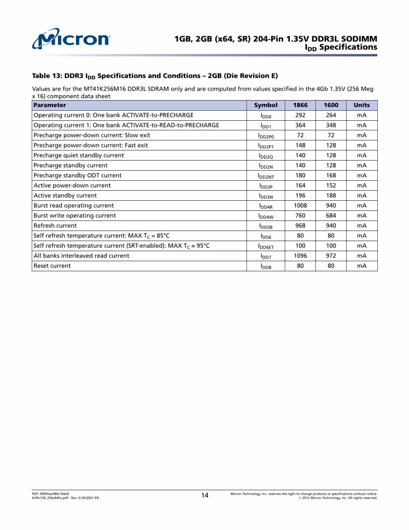
Table 13: DDR3 IDD Specifications and Conditions – 2GB (Die Revision E)
Values are for the MT41K256M16 DDR3L SDRAM only and are computed from values specified in the 4Gb 1.35V (256 Megx 16) component data sheetParameter Symbol 1866 1600 Units
Operating current 0: One bank ACTIVATE-to-PRECHARGE IDD0 292 264 mA
Operating current 1: One bank ACTIVATE-to-READ-to-PRECHARGE IDD1 364 348 mA
Precharge power-down current: Slow exit IDD2P0 72 72 mA
Precharge power-down current: Fast exit IDD2P1 148 128 mA
Precharge quiet standby current IDD2Q 140 128 mA
Precharge standby current IDD2N 140 128 mA
Precharge standby ODT current IDD2NT 180 168 mA
Active power-down current IDD3P 164 152 mA
Active standby current IDD3N 196 188 mA
Burst read operating current IDD4R 1008 940 mA
Burst write operating current IDD4W 760 684 mA
Refresh current IDD5B 968 940 mA
Self refresh temperature current: MAX TC = 85°C IDD6 80 80 mA
Self refresh temperature current (SRT-enabled): MAX TC = 95°C IDD6ET 100 100 mA
All banks interleaved read current IDD7 1096 972 mA
Reset current IDD8 80 80 mA
1GB, 2GB (x64, SR) 204-Pin 1.35V DDR3L SODIMMIDD Specifications
PDF: 09005aef84c19de9ktf4c128_256x64hz.pdf - Rev. G 05/2021 EN 14 Micron Technology, Inc. reserves the right to change products or specifications without notice.
© 2012 Micron Technology, Inc. All rights reserved.
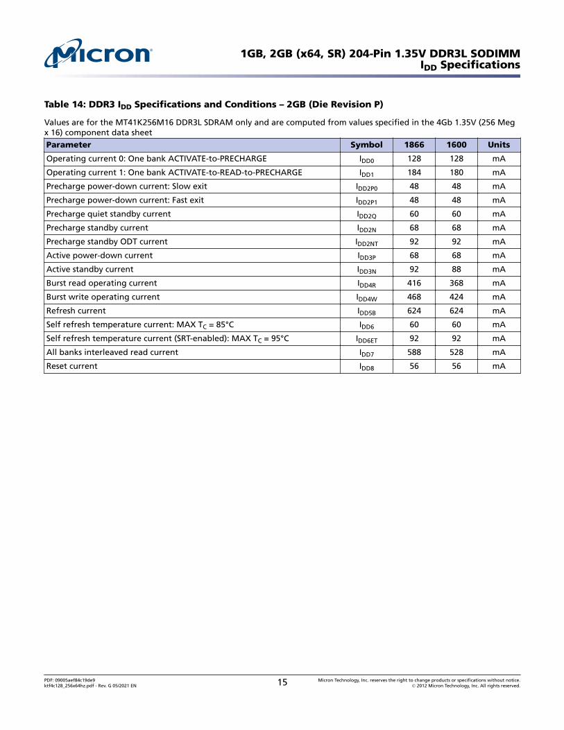
Table 14: DDR3 IDD Specifications and Conditions – 2GB (Die Revision P)
Values are for the MT41K256M16 DDR3L SDRAM only and are computed from values specified in the 4Gb 1.35V (256 Megx 16) component data sheetParameter Symbol 1866 1600 Units
Operating current 0: One bank ACTIVATE-to-PRECHARGE IDD0 128 128 mA
Operating current 1: One bank ACTIVATE-to-READ-to-PRECHARGE IDD1 184 180 mA
Precharge power-down current: Slow exit IDD2P0 48 48 mA
Precharge power-down current: Fast exit IDD2P1 48 48 mA
Precharge quiet standby current IDD2Q 60 60 mA
Precharge standby current IDD2N 68 68 mA
Precharge standby ODT current IDD2NT 92 92 mA
Active power-down current IDD3P 68 68 mA
Active standby current IDD3N 92 88 mA
Burst read operating current IDD4R 416 368 mA
Burst write operating current IDD4W 468 424 mA
Refresh current IDD5B 624 624 mA
Self refresh temperature current: MAX TC = 85°C IDD6 60 60 mA
Self refresh temperature current (SRT-enabled): MAX TC = 95°C IDD6ET 92 92 mA
All banks interleaved read current IDD7 588 528 mA
Reset current IDD8 56 56 mA
1GB, 2GB (x64, SR) 204-Pin 1.35V DDR3L SODIMMIDD Specifications
PDF: 09005aef84c19de9ktf4c128_256x64hz.pdf - Rev. G 05/2021 EN 15 Micron Technology, Inc. reserves the right to change products or specifications without notice.
© 2012 Micron Technology, Inc. All rights reserved.
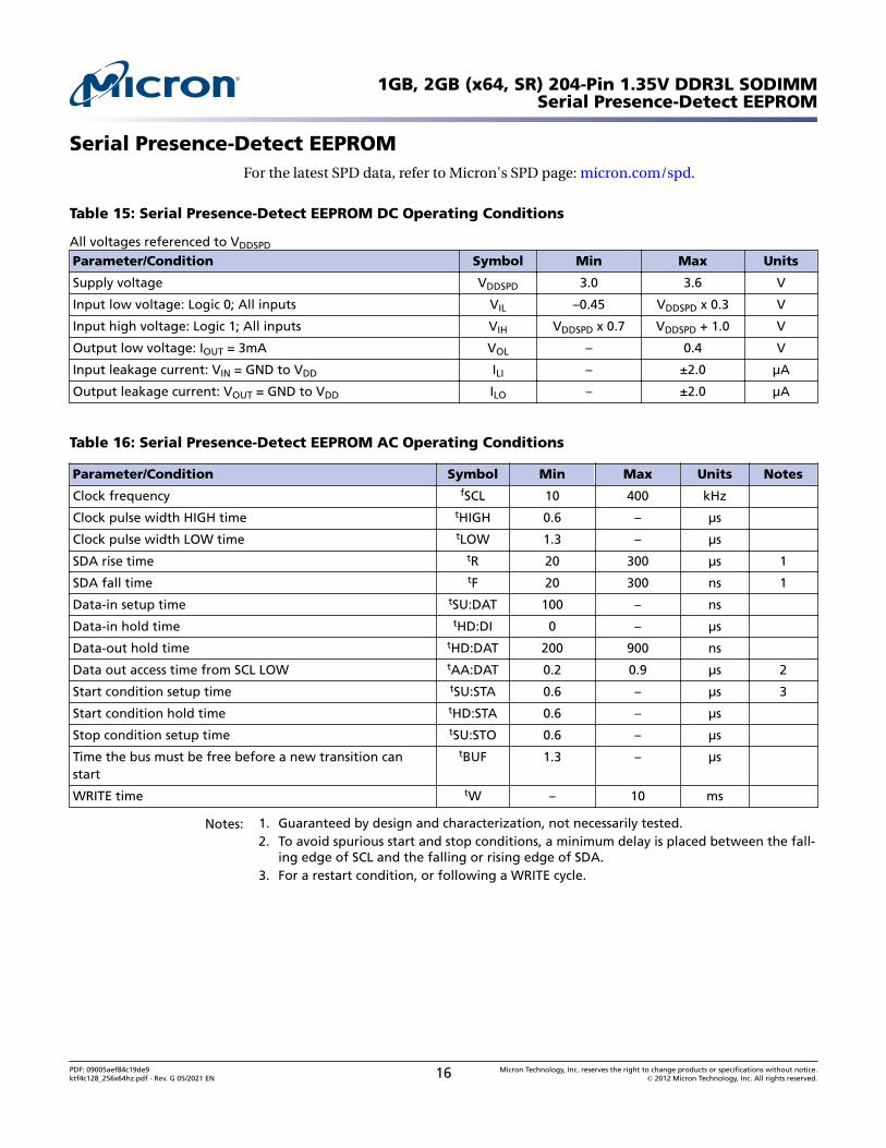
Serial Presence-Detect EEPROMFor the latest SPD data, refer to Micron's SPD page: micron.com/spd.
Table 15: Serial Presence-Detect EEPROM DC Operating Conditions
All voltages referenced to VDDSPD
Parameter/Condition Symbol Min Max Units
Supply voltage VDDSPD 3.0 3.6 V
Input low voltage: Logic 0; All inputs VIL –0.45 VDDSPD x 0.3 V
Input high voltage: Logic 1; All inputs VIH VDDSPD x 0.7 VDDSPD + 1.0 V
Output low voltage: IOUT = 3mA VOL – 0.4 V
Input leakage current: VIN = GND to VDD ILI – ±2.0 µA
Output leakage current: VOUT = GND to VDD ILO – ±2.0 µA
Table 16: Serial Presence-Detect EEPROM AC Operating Conditions
Parameter/Condition Symbol Min Max Units Notes
Clock frequency fSCL 10 400 kHz
Clock pulse width HIGH time tHIGH 0.6 – µs
Clock pulse width LOW time tLOW 1.3 – µs
SDA rise time tR 20 300 µs 1
SDA fall time tF 20 300 ns 1
Data-in setup time tSU:DAT 100 – ns
Data-in hold time tHD:DI 0 – µs
Data-out hold time tHD:DAT 200 900 ns
Data out access time from SCL LOW tAA:DAT 0.2 0.9 µs 2
Start condition setup time tSU:STA 0.6 – µs 3
Start condition hold time tHD:STA 0.6 – µs
Stop condition setup time tSU:STO 0.6 – µs
Time the bus must be free before a new transition canstart
tBUF 1.3 – µs
WRITE time tW – 10 ms
Notes: 1. Guaranteed by design and characterization, not necessarily tested.2. To avoid spurious start and stop conditions, a minimum delay is placed between the fall-
ing edge of SCL and the falling or rising edge of SDA.3. For a restart condition, or following a WRITE cycle.
1GB, 2GB (x64, SR) 204-Pin 1.35V DDR3L SODIMMSerial Presence-Detect EEPROM
PDF: 09005aef84c19de9ktf4c128_256x64hz.pdf - Rev. G 05/2021 EN 16 Micron Technology, Inc. reserves the right to change products or specifications without notice.
© 2012 Micron Technology, Inc. All rights reserved.
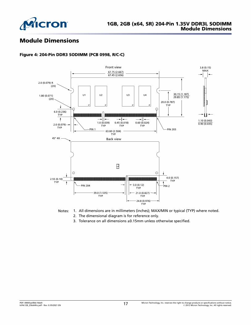
Module Dimensions
Figure 4: 204-Pin DDR3 SODIMM (PCB 0998, R/C-C)
3.8 (0.15)
MAX
PIN 1
67.75 (2.667)67.45 (2.656)
20.0 (0.787)TYP
1.80 (0.071)(2X)
0.60 (0.024) TYP
0.45 (0.018) TYP
2.0 (0.079) R(2X)
PIN 203
PIN 204 PIN 2
Front view
2.0 (0.079) TYP
6.0 (0.236) TYP
63.60 (2.504) TYP
2.55 (0.10) TYP
1.0 (0.039) TYP
30.15 (1.187)29.85 (1.175)
Back view
1.10 (0.043)0.90 (0.035)
39.0 (1.535) TYP
21.0 (0.827) TYP
3.0 (0.12) TYP
4.0 (0.157) TYP
24.8 (0.976) TYP
U1 U2 U3 U4
45° 4X
U8
Notes: 1. All dimensions are in millimeters (inches); MAX/MIN or typical (TYP) where noted.2. The dimensional diagram is for reference only.3. Tolerance on all dimensions ±0.15mm unless otherwise specified.
1GB, 2GB (x64, SR) 204-Pin 1.35V DDR3L SODIMMModule Dimensions
PDF: 09005aef84c19de9ktf4c128_256x64hz.pdf - Rev. G 05/2021 EN 17 Micron Technology, Inc. reserves the right to change products or specifications without notice.
© 2012 Micron Technology, Inc. All rights reserved.
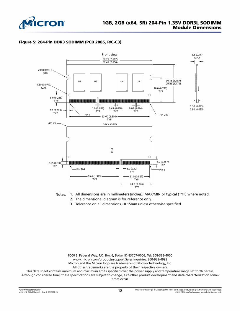
Figure 5: 204-Pin DDR3 SODIMM (PCB 2085, R/C-C3)
3.8 (0.15)
MAX
Pin 1
67.75 (2.667)67.45 (2.656)
20.0 (0.787)TYP
1.80 (0.071)(2X)
0.60 (0.024) TYP
0.45 (0.018) TYP
2.0 (0.079) R(2X)
Pin 203
Pin 204 Pin 2
Front view
2.0 (0.079) TYP
6.0 (0.236) TYP
63.60 (2.504) TYP
2.55 (0.10) TYP
1.0 (0.039) TYP
30.15 (1.187)29.85 (1.175)
Back view
1.10 (0.043)0.90 (0.035)
39.0 (1.535) TYP
21.0 (0.827) TYP
3.0 (0.12) TYP
4.0 (0.157) TYP
24.8 (0.976) TYP
45° 4X
U7
U1 U2 U4 U5
Notes: 1. All dimensions are in millimeters (inches); MAX/MIN or typical (TYP) where noted.2. The dimensional diagram is for reference only.3. Tolerance on all dimensions ±0.15mm unless otherwise specified.
8000 S. Federal Way, P.O. Box 6, Boise, ID 83707-0006, Tel: 208-368-4000www.micron.com/products/support Sales inquiries: 800-932-4992
Micron and the Micron logo are trademarks of Micron Technology, Inc.All other trademarks are the property of their respective owners.
This data sheet contains minimum and maximum limits specified over the power supply and temperature range set forth herein.Although considered final, these specifications are subject to change, as further product development and data characterization some-
times occur.
1GB, 2GB (x64, SR) 204-Pin 1.35V DDR3L SODIMMModule Dimensions
PDF: 09005aef84c19de9ktf4c128_256x64hz.pdf - Rev. G 05/2021 EN 18 Micron Technology, Inc. reserves the right to change products or specifications without notice.
© 2012 Micron Technology, Inc. All rights reserved.


![1Gb DDR3L (1.35V) SDRAM Specification...4.5 1.35 V DDR3L Electrical Characteristics and AC Timing ] 4.6 Address / Command Setup, Hold and Derating [Refer to section 4.1 in JEDEC Standard](https://img.pdfslide.us/doc/110x75/6118fdb29861ea1e5e6a2222/1gb-ddr3l-135v-sdram-specification-45-135-v-ddr3l-electrical-characteristics.jpg)