Embed Size (px)
Citation preview

International Journal of Science and Research (IJSR) ISSN (Online): 2319-7064
Index Copernicus Value (2013): 6.14 | Impact Factor (2013): 4.438
Volume 4 Issue 4, April 2015
www.ijsr.net Licensed Under Creative Commons Attribution CC BY
Performance Analysis of Three Phase T source
Inverter
G. Hemaprabha1, T. Rama Rajeswari
2, C. Subramanian
3
1Assistant Professor, Department of EEE, Info Institute of Engineering, India
2PG Student, Department of EEE, Info Institute of Engineering, India
3PG Student, Department of EEE, Bannari Amman Institute of Technology, India
Abstract: This paper investigates the performance analysis of T-source Inverter with simple boost control technique for boosting the
voltage. T-source impedance network is newly invented to overcome the drawbacks of Z-source inverter. In the literature, the basic
topology is called Z-source inverter (ZSI).It has less reactive components in comparing with conventional ZSI. The T source Network
can perform the dc to ac power conversion and also can perform buck boost operation at one stage. In ZSI the switches which are in the
same leg short circuit will takes place during switch on period. This voltage is stored by L and C circuit of z-source inverter. This stored
voltage is added with regular voltage when inverter is in normal operation-Source inverter implemented with simple boost control PWM
technique for boosting the voltage is simulated using MATLAB Simulink.
Keywords: Z-source inverter, T-Source inverter, Voltage gain, simple boost control, Shoot-through control
1. Introduction
The Inverter is an electrical system which converts direct
current to alternating current. It can consist of two traditional
inverters: voltage-source and current-source inverters. In
VSI, the output voltage cannot exceed the dc source voltage.
Dead time is needed to protect the upper and lower switching
devices in each phase leg from short circuit. In CSI, the
output voltage cannot be lower than the DC source. Overlap
time between phase legs is compulsory to avoid the open
circuit of upper or lower switching devices. These problems
are overcome in Z – source inverter and quasi Z – source
inverter. The TSI topology requires a very low leakage
inductance transformer which should be made with high
accurate output. It makes use of shoot through in the inverter
bridge to boost the voltage in the VSI due to the short circuit
occurrence or to buck the voltage in the CSI due to the open
circuit occurrence. The Z-source inverter is a buck–boost
inverter. It has more LC components. By using of T-source
inverter we can overcome the problems from ZSI.
2. Z-Source Inverter
The new improved L and C network has been introduced to
overcome the drawbacks of the traditional VSI and CSI
inverters. It can be used in ac/dc power conversion usages.
The power source may be either in the form of potential or
current form. The impedance network requires two inductors
and two capacitors connected to each other ZSI provides a
single-stage voltage buck and boost operation. Common LC
impedance network particularly improves the performance of
the inverter. It permits the state of shoot-through states to the
inverter legs during VSI (boost) operation as well as open
circuits of inverter legs during CSI (buck) operation.
Disadvantage of Z-Source Inverter:
Conventional two-stage buck-boost Systems are more
efficient than ZSI.
By the cause of high inductance the Z-source inverter
disturbed by over voltages during switches commutation.
Hence high rating of Switches are needed.
Z-source inverter produces discontinuous input current and
high values of di/dt due to that passive filter is needed at
input side.
3. T-Source Inverter
T-source impedance network is newly introduced to
overcome the problems of Z-source inverter. T-Source
Inverter is similar to Z-Source except the use of high
frequency low leakage inductance transformer and one
Capacitance. It has low reactive components in compare with
conventional ZSI. Due to this, the efficiency greatly
increases. The TSI topology requires a very low leakage
inductance transformer which should be made with high
accuracy. In such a way, the number of LC elements is
reduced because only the transformer and the capacitor are
needed. The T-Source Inverter topology functions as a
common DC rail between the source and inverter. It is not
same as the traditional Z-Source Inverter circuits. By use of a
transformer with other than a 1:1 transformer ratio allows for
a change of output voltage Z-source converters, as compared
with the voltage resulting from the shoot-through index or
the modulation index.
Figure 1: Circuit diagram for T-source Inverter
Paper ID: SUB153770 2906
International Journal of Science and Research (IJSR) ISSN (Online): 2319-7064
Index Copernicus Value (2013): 6.14 | Impact Factor (2013): 4.438
Volume 4 Issue 4, April 2015
www.ijsr.net Licensed Under Creative Commons Attribution CC BY
3.1 Principle of operation
There are two operating modes exists in T-source inverter.
One is active mode and another one is Shoot-through mode.
The T-network is used instead of the LC-network for
boosting the output voltage by inserting shoot through states
in the PWM.
3.2 Shoot through mode
Shoot through can be obtained inthree different ways such as
shoot through via one phase leg or combination of two phase
legs. The TSI can handle shoot through states when both
switches in the same phase leg are going to one state. In this
mode,diode is reverse biased and it separating DC link from
AC line.Desired output voltage can be obtain by controlling
the shoot through time.
Figure 2: Equivalent Circuit of shoot through state
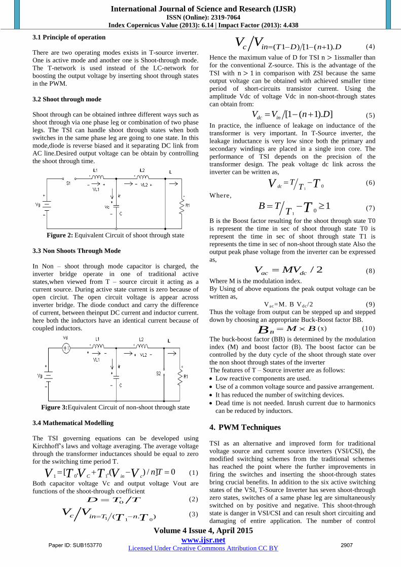
3.3 Non Shoots Through Mode
In Non – shoot through mode capacitor is charged, the
inverter bridge operate in one of traditional active
states,when viewed from T – source circuit it acting as a
current source. During active state current is zero because of
open circiut. The open circuit voltage is appear across
inverter bridge. The diode conduct and carry the difference
of current, between theinput DC current and inductor current.
here both the inductors have an identical current because of
coupled inductors.
Figure 3:Equivalent Circuit of non-shoot through state
3.4 Mathematical Modelling
The TSI governing equations can be developed using
Kirchhoff’s laws and voltage averaging. The average voltage
through the transformer inductances should be equal to zero
for the switching time period T.
0 11[ . .( ) / ] 0
C in cn TV V V VT T (1)
Both capacitor voltage Vc and output voltage Vout are
functions of the shoot-through coefficient
0D T T (2)
1 1 0( . )c in T n
V VT T
(3)
( 1 ) [1 ( 1).c in T D n DV V
(4)
Hence the maximum value of D for TSI n > 1issmaller than
for the conventional Z-source. This is the advantage of the
TSI with n > 1 in comparison with ZSI because the same
output voltage can be obtained with achieved smaller time
period of short-circuits transistor current. Using the
amplitude Vdc of voltage Vdc in non-shoot-through states
can obtain from:
[1 ( 1). ]dc inV V n D (5)
In practice, the influence of leakage on inductance of the
transformer is very important. In T-Source inverter, the
leakage inductance is very low since both the primary and
secondary windings are placed in a single iron core. The
performance of TSI depends on the precision of the
transformer design. The peak voltage dc link across the
inverter can be written as,
10dc
TTV T
(6)
Where,
10
1B TT T (7)
B is the Boost factor resulting for the shoot through state T0
is represent the time in sec of shoot through state T0 is
represent the time in sec of shoot through state T1 is
represents the time in sec of non-shoot through state Also the
output peak phase voltage from the inverter can be expressed
as,
/ 2ac dcV MV (8)
Where M is the modulation index.
By Using of above equations the peak output voltage can be
written as,
Vac=M. B Vdc/2 (9)
Thus the voltage from output can be stepped up and stepped
down by choosing an appropriate Buck-Boost factor BB.
BM BB (x) (10)
The buck-boost factor (BB) is determined by the modulation
index (M) and boost factor (B). The boost factor can be
controlled by the duty cycle of the shoot through state over
the non shoot through states of the inverter
The features of T – Source inverter are as follows:
Low reactive components are used.
Use of a common voltage source and passive arrangement.
It has reduced the number of switching devices.
Dead time is not needed. Inrush current due to harmonics
can be reduced by inductors.
4. PWM Techniques
TSI as an alternative and improved form for traditional
voltage source and current source inverters (VSI/CSI), the
modified switching schemes from the traditional schemes
has reached the point where the further improvements in
firing the switches and inserting the shoot-through states
bring crucial benefits. In addition to the six active switching
states of the VSI, T-Source Inverter has seven shoot-through
zero states, switches of a same phase leg are simultaneously
switched on by positive and negative. This shoot-through
state is danger in VSI/CSI and can result short circuiting and
damaging of entire application. The number of control
Paper ID: SUB153770 2907
International Journal of Science and Research (IJSR) ISSN (Online): 2319-7064
Index Copernicus Value (2013): 6.14 | Impact Factor (2013): 4.438
Volume 4 Issue 4, April 2015
www.ijsr.net Licensed Under Creative Commons Attribution CC BY
methods to control T-source inverter, which include the
sinusoidal PWM techniques, there are three types of Pulse
Width Modulation control algorithms exists: simple boost
control (SBC), Maximum boost control (MBC), constant
boost control (CBC).
The modulation index also defined as amplitude modulation
ratio (M) which is the main control factor is defined as the
ratio of amplitude of reference wave to the amplitude of
carrier wave
/ref caM V V
The linearity between the modulation index and the output
voltage is achieved by under the modulation index (M < 1).
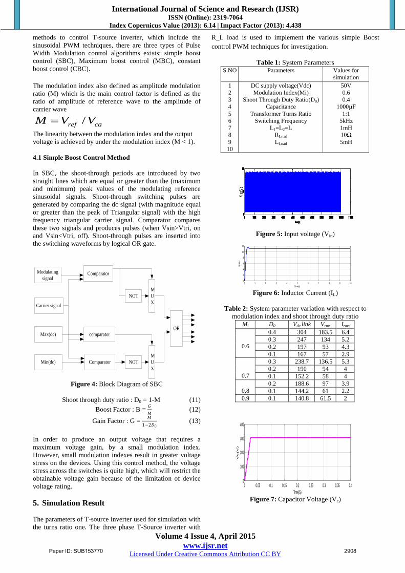
4.1 Simple Boost Control Method
In SBC, the shoot-through periods are introduced by two
straight lines which are equal or greater than the (maximum
and minimum) peak values of the modulating reference
sinusoidal signals. Shoot-through switching pulses are
generated by comparing the dc signal (with magnitude equal
or greater than the peak of Triangular signal) with the high
frequency triangular carrier signal. Comparator compares
these two signals and produces pulses (when Vsin>Vtri, on
and Vsin<Vtri, off). Shoot-through pulses are inserted into
the switching waveforms by logical OR gate.
Modulating
signalComparator
Carrier signal
Max(dc) comparator
Min(dc) Comparator
M
U
X
NOT
M
U
X
NOT
OR
Figure 4: Block Diagram of SBC
Shoot through duty ratio : D0 = 1-M (11)
Boost Factor : B = 𝐺
𝑀 (12)
Gain Factor : G = 𝑀
1−2𝐷0 (13)
In order to produce an output voltage that requires a
maximum voltage gain, by a small modulation index.
However, small modulation indexes result in greater voltage
stress on the devices. Using this control method, the voltage
stress across the switches is quite high, which will restrict the
obtainable voltage gain because of the limitation of device
voltage rating.
5. Simulation Result
The parameters of T-source inverter used for simulation with
the turns ratio one. The three phase T-Source inverter with
R_L load is used to implement the various simple Boost
control PWM techniques for investigation.
Table 1: System Parameters S.NO Parameters Values for
simulation
1
2
3
4
5
6
7
8
9
10
DC supply voltage(Vdc)
Modulation Index(Mi)
Shoot Through Duty Ratio(D0)
Capacitance
Transformer Turns Ratio
Switching Frequency
L1=L2=L
RLoad
LLoad
50V
0.6
0.4
1000µF
1:1
5kHz
1mH
10Ω
5mH
Figure 5: Input voltage (Vin)
Figure 6: Inductor Current (IL)
Table 2: System parameter variation with respect to
modulation index and shoot through duty ratio Mi D0 Vdc link Vrms Irms
0.6
0.4 304 183.5 6.4
0.3 247 134 5.2
0.2 197 93 4.3
0.1 167 57 2.9
0.7
0.3 238.7 136.5 5.3
0.2 190 94 4
0.1 152.2 58 4
0.8
0.2 188.6 97 3.9
0.1 144.2 61 2.2
0.9 0.1 140.8 61.5 2
Figure 7: Capacitor Voltage (Vc)
0 1 2 3 4 5 6 7 8 8 100
2
4
6
8
10
12
Time(s)
Ilin
(A)
0 0.05 0.1 0.15 0.2 0.25 0.3 0.35 0.40
100
200
300
400
Time(S)
Vc(V
)
Paper ID: SUB153770 2908
International Journal of Science and Research (IJSR) ISSN (Online): 2319-7064
Index Copernicus Value (2013): 6.14 | Impact Factor (2013): 4.438
Volume 4 Issue 4, April 2015
www.ijsr.net Licensed Under Creative Commons Attribution CC BY
Figure 8: Inverter line to line voltage without filter(VL)
Figure 9: Load Current (IL)
Figure 10: Voltage across load (VLL)
Figure 11: Output current of Harmonic spectrum
Figure 12: Harmonics spectrum of the Output voltage
Table 3: The profile of Harmonics
D0
ZSI Proposed TSI
V_thd I_thd V_thd I_thd
0.4 42.2 5.02 27.1 4.79
0.3 41.9 4.9 27.1 4.59
0.2 40.9 4.7 26.95 4.05
0.1 40.2 4.62 26.9 4.03
The harmonic profile of the output voltage and current of
TSI with Maximum boost control method. Total harmonic
distortion of proposed TSI is low compared to Z-Source
inverter of same rating. Figure 11 and Figure 12 illustrates
the harmonic spectrum of load current and load voltage
6. Conclusion
This research deals with the Analysis of T-source inverter
with simple boost control technique for improving voltage
gain. The T-source inverter overcomes the problems of the
Z-source inverter and provides buck-boost operation in a
single stage. The T-source impedance network provide the
output voltage larger than the input voltage by proper
maintaining the duty ratio of shoot-through state, voltage-
source inverter and current-source inverter can’t be provide
these advantages. When compared with ZSI, the T-source
inverter has less passive components .All Pulse Width
Modulation methods can be used to control T-source
inverter. In this research deals with simple boost control
techniques which are used to control the T-source inverter.
References
[1] S.Thangaprakash, A. Krishnan “Implementation and
Critical Investigation on Modulation Schemes of Three
Phase Impedance Source Inverter” Iranian Journal of
Electrical & Electronic Engineering, 88 Vol. 6, No. 2,
June 2010
[2] Poh Chiang Loh, , D. Mahinda Vilathgamuwa, , Yue
Sen Lai, Geok Tin Chua, and Yunwei Li, “ Pulse -
Width Modulation of Z – source Inverters” IEEE
Transactions on Power Electronics, Vol. 20, No. 6,
November 2005.
[3] Sivaraman.P, A. Nirmalkumar, “ Modelling and
Simulation of Photovoltaic Array fed T-Source Inverter”
in International Conference onSustainable Energy and
Intelligent System ,2011.
[4] Sivaraman.P, A. Nirmalkumar, “Analysis and
Implementation of Novel TSI for High Voltage Gain
Application” in International Review on Modelling and
Simulations,2010
[5] Sivaraman.P, A. Nirmalkumar, “Analysis of T-Source
Inverter with Various PWM Schemes” in European
Journal of Scientific Research,Vol.71 No.2 , pp. 203-
213,2012
[6] F. Z. Peng: Z-Source Networks for Power Conversion,
Proc. of 23rd
Annual IEEE APEC’08, 2008, pp. 1258-
1265
[7] F.Z. Peng, “Z source inverter”, IEEE Trans.
IndustryApplications,vol. 39, no. 2, pp. 504-510,
March/April 2003.
[8] J. Rabkowski, R. Barlik, and M. Nowak, “Pulse
WidthModulationmethods for bidirectional/high-
performance Z-source inverter”, IEEEPower Electronics
Specialists Conference, pp. 2750 –2756, June 2008.
[9] Marek Adamowicsz, Natalia Strzeleckal and Wieslaw
Bury “New type T-source inverter” In proceeding on
international conference of compatibility in power
Electronics-2009 pp-191-195.
[10] Sivaraman P and Nirmal kumar A, “Analysis and
implementation of a novel T-source inverter for high
voltage gain application”International Review of
Modeling and Simulation vol.5 pp 818-825 April 2012
ISSN 1974-9821.
2200 2250 2300 2350 2400 2450 2500-1000
-500
0
500
1000
Time(ms)
VL(V
)
200 220 240 260 280-9
-6
0
6
9
Time(ms)
IL(A
)
200 220 240 260 280 300
-200
-100
0
100
200
Time(ms)
VL
L(V
)
Paper ID: SUB153770 2909
International Journal of Science and Research (IJSR) ISSN (Online): 2319-7064
Index Copernicus Value (2013): 6.14 | Impact Factor (2013): 4.438
Volume 4 Issue 4, April 2015
www.ijsr.net Licensed Under Creative Commons Attribution CC BY
[11] Power Electronics Circuits, Devices and applications by
M.H Rashid, 3rd
edition, Pearson Education – 2004
[12] F. Z. Peng, “Z-source inverter”, IEEE Transactions on
IndustryApplications, Vol. 39, No. 2, pp. 504-510, 2003
[13] F. Z. Peng, M. Shen, Z. Qian, “Maximum boost control
of the Z-source inverter”, IEEE Transactions on Power
Electronics, Vol. 20, No. 4, pp.833-838, 2005
[14] P. C. Loh, D. M. Vilathgamuwa, Y. S. Lai, G. T. Chua,
Y. Li, “Pulsewidthmodulation of Z-source inverters”,
IEEE Transactions on Power Electronics, Vol. 20, No. 6,
pp. 1346-1355, 2005
Paper ID: SUB153770 2910