Embed Size (px)
Citation preview
Journal of Babylon University/Pure and Applied Sciences/ No.(5)/ Vol.(19): 2011
4012
Design of a 31-Level Single-Phase Voltage-source Inverter Producing almost Sinusoidal
Voltage Waveform
Abdul-Kareem M. Obais
Department of Electrical Eng, College of Engineering, University of Babylon
Abstract In this paper a single-phase voltage-source inverter of 31 non-zero levels is designed. These
levels follow a sinusoidal path and are constructed by using only five dc voltage sources instead of
thirty-one as traditionally employed in multilevel technology of voltage-source inverters.
Consequently, the total numbers of switching devices and electronic circuitries are largely reduced. The
output voltage of this inverter has sinusoidal form and is almost free from harmonics associating
conventional types of inverters. No type of conventional Pulse-Width-Modulation is introduced here
and the technique is applicable for both resistive and inductive loads. The complete system was
designed and implemented on Pspice.
الخلاصةغير صفري متساوية ى مستو وثلاثين واحدالطور ذات ةأحادي فولتية عاكس لمفولتية يقوم بتوليدفي هذا العمل تم تصميم
إحدى وتلانين التيار المباشر بدلا من التباعد وتتبع مسارا جيبي الشكل. هذه المستويات تم تشكيمها باستخدام خمسة مصادر لفولتيةصاحب هذا التخفيض في عدد و الفولتيات المتعددة المستويات. إنتاجهو مستخدم في التقنيات التقميدية التي تتبنى مصدرا كمافولتية الإخراج لهذا العاكس ذات شكل جيبي وخالي والدوائر الالكترونية اللازمة لها. الأجهزة المفتاحيةكبير في عدد اتخفيضالمصادر
هذه و لمعاكسات التقميدية. لم يستخدم في هذا النظام أي نوع من أنواع تعديل عرض النبضة التقميدي. زمةتقريبا من التوافقيات الملا .(PSpiceألتشبيهي ) جالتقنية ملائمة للأحمال الحثية والأحمال ذات المقاومة النقية. تم إجراء التصميم واختباره باستخدام البرنام
1. Introduction Inverters are the most efficient means of dc to ac power conversion and have
an important role in variable ac drive industries. They witnessed an excessive
hierarchy of developments throughout the recent years. The multilevel technology is
one of those developments where the shaping of the output voltage waveforms of
inverters has been assigned as the main target of this technology. Efforts were exerted
to construct sinusoidal voltage waveforms at the output of voltage source inverters.
The space-vector techniques had adopted the achievement of output voltages
constituting sinusoidal envelopes with their average values (Teodorescu et al 2002,
Mailah et al 2009). Those techniques had employed intelligent gate drive to design
microcontrollers for triggering the switching devices of voltage-source inverters.
Researchers, who are interested in multilevel techniques, aspire to approach
sinusoidal voltage waveforms at the output of voltage-source inverters (Tolbert et al
1999, Mekhilef and Masaoud 2006, Pandian and Reddy 2008), but this requires large
numbers of dc voltage sources and switching devices, in addition to the complex
circuitry associating them. Since the number of voltage levels is restricted by the
complexity of the inverter circuitry, designers tend to accept limited levels and treat
each level by a certain Pulse-Width-Modulation technique besides a proper harmonics
elimination technique (Manguelle and Rufer 2001, Kumar et al 2008). Here in the
adopted design, thirty-one non-zero levels were constructed for each half cycle of the
single-phase voltage at the output of the voltage-source inverter using only five
separate dc voltage sources and no type of conventional Pulse-Width-Modulation was
employed.

4012
2. Construction of a 31-nonzero level unidirectional voltage supply The system employs five dc voltage sources to construct thirty-one nonzero
voltage levels. Fig. 1 states the technique that achieves the above strategy. The
multilevel voltage Vmlt is simply the resultant of the activated voltages of the five dc
sources, which are controlled by the logic of the five most significant digits of an 8-bit
analog-to-digital converter (8-bit ADC). The dc voltage sources are weighted
according to the weights of digits controlling them.
If the input of the ADC is the positive half cycle of a sinusoidal voltage signal
having amplitude of 10 volts and frequency of 50Hz, then the voltage Vmlt will
exhibit the voltage waveform shown in Fig. 2. Here, Vb represents the voltage step,
which is simply the difference between two adjacent levels and is denoted by the base
voltage. The five dc voltage sources will be Vb, 2Vb, 4Vb, 8Vb, and 16Vb according to
the weights of the five most significant digits controlling their switches Z1, Z2, Z3,
Z4, and Z5. For example, DB3, DB4, DB5, DB6, and DB7 control the voltage sources
Vb, 2Vb, 4Vb, 8Vb, and 16Vb respectively, while the switches Z1*, Z2*, Z3*, Z4*, and
Z5* are controlled by the complements DB3*, DB4*, DB5*, DB6*, and DB7*
respectively. Consequently, when a certain Z switch is in OFF state, then the
corresponding Z* switch will be in ON state and vice versa. Table (1) shows the truth
table of the controlling logic, the status of the switching devices, and the
corresponding values of Vmlt.
Fig . 1 The multilevel voltage production circuit.
-
+
Vmlt
DB7
DB6
DB5
DB4
DB7*
DB3
DB3*
DB4*
DB5*
DB6*
Z3
Z3*
Z2
Z2*
Z1
Z1*
16Vb
8Vb
Z5*
2Vb
4Vb
Vb
Z5
Z4*
Z4
32Vb
24Vb
16Vb
Time
0s 5ms 10ms
V(U4:OUT)
0V
5V
10V
15V
Volt
age
lev
el

Journal of Babylon University/Pure and Applied Sciences/ No.(5)/ Vol.(19): 2011
4012
Table (1) The truth table of the 31- level voltage supply. DB7 DB6 DB5 DB4 DB3 Z5 Z4 Z3 Z2 Z1 Z5* Z4* Z3* Z2* Z1* Vmlt
0 0 0 0 0 OFF OFF OFF OFF OFF ON ON ON ON ON 0
0 0 0 0 1 OFF OFF OFF OFF ON ON ON ON ON OFF Vb
0 0 0 1 0 OFF OFF OFF ON OFF ON ON ON OFF ON 2Vb
0 0 0 1 1 OFF OFF OFF ON ON ON ON ON OFF OFF 3Vb
0 0 1 0 0 OFF OFF ON OFF OFF ON ON OFF ON ON 4Vb
0 0 1 0 1 OFF OFF ON OFF ON ON ON OFF ON OFF 5Vb
0 0 1 1 0 OFF OFF ON ON OFF ON ON OFF OFF ON 6Vb
0 0 1 1 1 OFF OFF ON ON ON ON ON OFF OFF OFF 7Vb
0 1 0 0 0 OFF ON OFF OFF OFF ON OFF ON ON ON 8Vb
0 1 0 0 1 OFF ON OFF OFF ON ON OFF ON ON OFF 9Vb
0 1 0 1 0 OFF ON OFF ON OFF ON OFF ON OFF ON 10Vb
0 1 0 1 1 OFF ON OFF ON ON ON OFF ON OFF OFF 11Vb
0 1 1 0 0 OFF ON ON OFF OFF ON OFF OFF ON ON 12Vb
0 1 1 0 1 OFF ON ON OFF ON ON OFF OFF ON OFF 13Vb
0 1 1 1 0 OFF ON ON ON OFF ON OFF OFF OFF ON 14Vb
0 1 1 1 1 OFF ON ON ON ON ON OFF OFF OFF OFF 15Vb
1 0 0 0 0 ON OFF OFF OFF OFF OFF ON ON ON ON 16Vb
1 0 0 0 1 ON OFF OFF OFF ON OFF ON ON ON OFF 17Vb
1 0 0 1 0 ON OFF OFF ON OFF OFF ON ON OFF ON 18Vb
1 0 0 1 1 ON OFF OFF ON ON OFF ON ON OFF OFF 19Vb
1 0 1 0 0 ON OFF ON OFF OFF OFF ON OFF ON ON 20Vb
1 0 1 0 1 ON OFF ON OFF ON OFF ON OFF ON OFF 21Vb
1 0 1 1 0 ON OFF ON ON OFF OFF ON OFF OFF ON 22Vb
1 0 1 1 1 ON OFF ON ON ON OFF ON OFF OFF OFF 23Vb
1 1 0 0 0 ON ON OFF OFF OFF OFF OFF ON ON ON 24Vb
1 1 0 0 1 ON ON OFF OFF ON OFF OFF ON ON OFF 25Vb
1 1 0 1 0 ON ON OFF ON OFF OFF OFF ON OFF ON 26Vb
1 1 0 1 1 ON ON OFF ON ON OFF OFF ON OFF OFF 27Vb
1 1 1 0 0 ON ON ON OFF OFF OFF OFF OFF ON ON 28Vb
1 1 1 0 1 ON ON ON OFF ON OFF OFF OFF ON OFF 29Vb
1 1 1 1 0 ON ON ON ON OFF OFF OFF OFF OFF ON 30Vb
1 1 1 1 1 ON ON ON ON ON OFF OFF OFF OFF OFF 31Vb
When a precision full-wave rectifier for a 10V peak sinusoidal waveform,
produces the analogue input to the 8-bit ADC, the path of thirty-one voltage levels of
Vmlt will follow the shape of the positive halves of a sinusoidal voltage waveform as
shown in Fig .3a. The multilevel voltage Vmlt will actually be the main supply of a
somewhat modified single-phase voltage-source inverter bridge to form the sought
inverter. Since the conventional single-phase voltage-source inverter is characterized
by reversing the current and voltage through the load, its output will attain sinusoidal
form as shown in Fig.3b.

4012
2.1 The fundamental component of the inverter load voltage A seven nonzero-level voltage is suggested here for simplifying the derivation
of the fundamental component of any N-level load voltage. Fig. 4 shows this voltage.
Vmsinωt is the voltage desired to be generated. It is a sinusoidal voltage of amplitude
Vm and angular frequency ω. VL is the multilevel voltage, which is built of seven-
nonzero levels. Note that the total number of voltage levels (including the zero level)
is eight and the voltage step (Vb) is Vm/8. If a multilevel voltage of N-nonzero
levels is required to be constructed, then the voltage step will be {Vm/(N+1)}.
Substituting for ωt by θ, the height of the shaded rectangular in Fig. 4 is given by:
kb VmkV sin ……………………………………….. (1)
Where K is the number of a certain voltage level and varies from 0 to N. θk is equated
to be:
Mult
ilev
el v
olt
age
Supply
, V
lmt
32Vb
24Vb
16Vb
8Vb
0Vb
Time
0s 5ms 10ms 15ms 20ms
V(U4:OUT)
0V
5V
10V
15V
(a)
Time
0s 5ms 10ms
V(U4:OUT)
0V
5V
10V
15V
Time
0s5ms10ms
V(U4:OUT)
0V
5V
10V
15V
32Vb
16Vb
0Vb
-16Vb
-32Vb
Time
0s 5ms 10ms 15ms 20ms
V(U4:OUT)
0V
5V
10V
15V
Inver
ter
Load
volt
age
(b)
Fig. 3 (a) The 31-level voltage supply, (b) the inverter load voltage.

Journal of Babylon University/Pure and Applied Sciences/ No.(5)/ Vol.(19): 2011
4012
VmkVb
k
1
sin
1sin
1
Nk
……………………………… (2)
Where Vm/Vb = N+1.
The fundamental component a1 of the load voltage VL is determined by using
Fourier series as follows (Wylie 1975):
dVa L2
01 sin1
dkV
k
kb
Nk
k
1
sin4
0
1
0
coscos4
kk
Nk
k
bkV
22
01
11
11
4N
kN
kkVNk
k
b
....... (3)
The ratio (a1/Vm) is computed for values of N from 3 to 255 and then plotted
against these values as shown in Fig. 5. It is obvious that this ratio tends to unity
while N is increasing. Table (2) shows the numeric variations of a1/Vm and Vb
against N when Vm is 320 volts. It is recommended here to mention that the operating
frequency of VL is unlimited, but it is obviously understood to be within the usual ac
drive ranges.
Time
0s 5ms 10ms
V(R7:2) V(U1:+)
0V
5V
10V
Time
0s5ms10ms
V(R7:2)V(U1:+)
0V
5V
10V
Vm=(N+1)Vb
NVb
θk
θk+1
kV
b
π/2 π 0
3π/2 2π
θ
Vmsinθ
VL
Fig . 4 Seven-level voltage construction.
Fig. 5 The ratio (a1/Vm) against the number of nonzero voltage
levels.
0.7
0.720.74
0.760.78
0.80.82
0.840.86
0.88
0.90.92
0.940.96
0.981
1.02
0 20 40 60 80 100 120 140 160 180 200 220 240 260
Number of nonzero voltage levels
Th
e r
ati
o (
a1/V
m)

4012
Table (2) The variations of load voltage fundamental with nonzero levels.
3.
The proposed inverter design scheme The schematic diagram of the proposed inverter is shown in Fig. 6. The 50Hz
signal having amplitude of 10V is full-wave rectified and fed to the 8-bit ADC, which
converts it to digital at a frequency of 100 KHz. The five most significant digits of the
8-bit ADC are employed with their complements to control the Z and the Z*
switching devices which are insulated-gate-transistors driven by proper electrically
insulated electronic circuits. The positive and negative half cycles of the load voltage
are demonstrated according the voltage-source bridge performance constructed by S1,
S2, S3, and S4.
Number of nonzero
voltage levels, N Fundamental
component, a1 (volts) Base voltage, Vb
(volts) Percentage (a1/Vm)
(100%)
3 254.34 80 79.17
7 289.41 40 90.44
15 305.55 20 95.484
31 313.13 10 97.85
63 316.74 5 98.98
127 318.49 2.5 99.52
255 319.34 1.25 99.79
Z3*
Z3
Z2*
Z2
8-bit
analog-to-digital
converter
Zero-crossing
detector
50Hz
sinusoidal
generator
100KHz
square-wave
generator
Start of
conversion
Analogue input
(0 to 10V)
DB2
DB3
DB4
DB5
DB6
DB7
Least signifigant digits
Most signifigant digits
DBo
DB1
1 2
3 4
5 6
9 8
11 10
Driving
circuit of Z5*
Driving
circuit of Z4
Driving
circuit of Z4*
Driving
circuit of Z3
Driving
circuit of Z3*
11 10
Driving
circuit of Z2
Driving
circuit of Z2*
Driving
circuit of Z1
Driving
circuit of Z1*
Driving
circuit of S1
Driving
circuit of S3
Driving
circuit of S4
Driving
circuit of S2
Z1
Z1*
Controlling circuit Driving circuit Power circuit
16Vb
Driving
circuit of Z5
8Vb
Z5*
0
4Vb
S1
S4
2Vb
Vb
S3
S2
Z5
Z4*
Z4
0
Full-wave
precision
rectifier
Load
Fig. 6 The proposed inveter schematic design.

Journal of Babylon University/Pure and Applied Sciences/ No.(5)/ Vol.(19): 2011
4001
The 31-non-zero levels inverter circuit diagram: Fig. 7 shows the whole system circuit diagram which is designed on PSpice.
All the datasheets of the electronic parts were taken into account during the design
process. It is recommended here to concern the circuits of this diagram separately for
the sake of stating the system performance. The circuit diagram follows the schematic
diagram shown in Fig. 7 and hence there are three main circuits to be identified here.
V16
15v
U1
7
A4
N2
5A
VL
Q16
Q2
N3
90
4
A
Q17
Q2
N3
90
4R
41
1k
R4
250
0
Vs
R4
35
GS
1Q
18
Q2
N3
90
6
U1
8A
CL
C4
28
/CL
OU
T1
V+
8
V-
4
+3
-2
-5v
+5v
R4
45k
R4
55k
R4
6
22
V17
15v
U1
9
A4
N2
5A
iFWC
GS
1
GZ
3*
GS
2
SL
C1
Z5*
IRG
BC
40
F
Z4*
IRG
BC
40
F
DS
2
HF
A2
5TB
60
3 1
Z3*
IRG
BC
40
FDS
4
HF
A2
5TB
60
3 1
Z2*
IRG
BC
40
F
Z1*
IRG
BC
40
F
L2
5uH
S1
IRG
BC
40
F
S4
IRG
BC
40
F
C5
FW
D2
HF
A2
5TB
60
31
GZ
2*
S2
IRG
BC
40
F
Smoothing circuit
GZ
1*
Compensating voltage
C4
GZ
5
GS
4
0
GZ
4
GS
3
GZ
2
GZ
3
GZ
1
V1
10v
Driving circuit of Z*5
S3
IRG
BC
40
F
V2
20v
V3
40v
Q19
Q2
N3
90
4
V4
80v
Q20
Q2
N3
90
4R
47
1k
L
C4
1uF
C3
R4
850
V5
160v
DS
1
HFA25TB60
3 1
Vs
*
Driving circuit of Z5
0
DS
3
HFA25TB603 1
R4
95
GS
4
RPower circuit
Q21
Q2
N3
90
6
Z1
0
IRG
BC
40
F
A
Z2
IRG
BC
40
F
U2
0A
CL
C4
28
/CL
OU
T1
V+
8
V-
4
+3
-2
-5v
+5v
R5
05k
R5
15k
C2
Z3
IRG
BC
40
F
R5
2
22
B
V18
15v
Z4
IRG
BC
40
F
U2
1
A4
N2
5A
GZ
5*
Z5
IRG
BC
40
F
GZ
4*
0
C2
150uF
Load
Driving circuit of Z2
Driving circuit of Z3
Driving circuit of Z4
Driving circuit
Freewheeling circuit
iSm
C1
10uF
DS
M
HFA25TB60
3 1
0
L1
10uH
FW
D1
HF
A2
5TB
60
31
Driving circuit of S2
Driving circuit of S3
Driving circuit of Z1
DB
6
0
Vs
Q22
Q2
N3
90
4
C5
Q23
Q2
N3
90
4R
53
1k
R5
450
DB
7
0
R5
55
Analog-to-digital converter
GZ
5Q
24
Q2
N3
90
6
U2
2A
CL
C4
28
/CL
OU
T1
V+
8
V-
4
+3
-2
-5v
+5v
R5
65k
R5
75k
U3
AD
C8
bre
ak
DB
716
DB
615
DB
514
DB
413
DB
312
DB
211
DB
110
DB
09
AG
ND
8
IN1
CN
VR
T2
STA
T3
OV
ER
4
RE
F5
R5
8
22
V19
15v
0
R5
5k
U2
3
A4
N2
5A
R6
5k
DB
6*
V11
10v
0
00
0 CLK
DS
TM
1
OF
FT
IME
= 5
us
ON
TIM
E =
5u
sD
EL
AY
= 0
STA
RT
VA
L =
0O
PP
VA
L =
1
0
+5v
R1
01k
+15v
0-1
5v
U4
LM
67
5
+1
-2
V+
5
V-
3
OU
T4
DB
5
0
R7
10k
R8
1k
R9
1.2
k
D5
BA
W6
2
D6
BA
W6
2
Driving circuit of S4
-5v
0
V7
5v
+5v
V8
5v
-5v
Vs
*
V9
15v
V10
15v
-15v
+15v
0
0
+15v
-15v
V26
FR
EQ
= 5
0H
zV
AM
PL
= 1
0v
VO
FF
= 0
-15v
+15v
R1
1k
R4
1k
R2
1k
D2
BA
W6
2
D4
BA
W6
2
0
U1
LM
67
5
+1
-2
V+
5
V-
3
OU
T4
U2
LM
67
5
+1
-2
V+
5
V-
3
OU
T4
D1
BA
W6
2
D3
BA
W6
2
Q25
Q2
N3
90
4
C4
Q26
Q2
N3
90
4R
59
1k
R6
050
DB
6
0
R6
15
GZ
4Q
27
Q2
N3
90
6
U2
4A
CL
C4
28
/CL
OU
T1
V+
8
V-
4
+3
-2
+5v
-5v
DB
4
R6
25k
R6
35k
R6
4
22
V20
15v
U2
5
A4
N2
5A
Zero-crossing detector
Driving circuit of S1
DB
3
Q28
Q2
N3
90
4
C3
Q29
Q2
N3
90
4R
65
1k
R6
650
DB
5*
0
DB
5
R6
75
GZ
3Q
30
Q2
N3
90
6
Driving circuit of Z*4
Driving circuit of Z*3
Driving circuit of Z*2
Driving circuit of Z*1
U2
6A
CL
C4
28
/CL
OU
T1
V+
8
V-
4
+3
-2
-5v
+5v
R6
85k
R6
95k
R7
0
22
V21
15v
U2
7
A4
N2
5A
Q31
Q2
N3
90
4
C2
Q32
Q2
N3
90
4
Precision full-wave rectifier
R7
11k
R7
250
U5
A
CL
C4
28
/CL
OU
T1
V+
8
V-
4
+3
-2
DB
4
0
R7
35
GZ
2Q
33
Q2
N3
90
6
U2
8A
CL
C4
28
/CL
OU
T1
V+
8
V-
4
+3
-2
+5v
-5v
R7
45k
R7
55k
R7
6
22
V22
15v
iL
U2
9
A4
N2
5A
U6
A
7404
12
U6
B
7404
34
U6
C
7404
56
DB
4*
U6
D
7404
98
U6
E
7404
11
10
U6
F
7404
13
12
DB
7
Q34
Q2
N3
90
4
C1
Q35
Q2
N3
90
4R
77
1k
R7
850
V6
10V
DB
3
0
R7
95
GZ
1Q
36
Q2
N3
90
6
U3
0A
CL
C4
28
/CL
OU
T1
V+
8
V-
4
+3
-2
-5v
+5v
R8
05k
R8
15k
R8
2
22
V23
15v
U3
1
A4
N2
5A
Q1
Q2
N3
90
4
C5
Q2
Q2
N3
90
4R
14
1k
R1
550
DB
7*
0
R1
65
GZ
5*
Q3
Q2
N3
90
6
Q37
Q2
N3
90
4
U8
A
CL
C4
28
/CL
OU
T1
V+
8
V-
4
+3
-2
+5v
B
Q38
Q2
N3
90
4
-5v
R8
31k
R1
25k
R1
35k
R8
450
R1
1
22
V12
15v
Vs
*
U9
A4
N2
5A
0
R8
55
GS
3Q
39
Q2
N3
90
6
U3
2A
CL
C4
28
/CL
OU
T1
V+
8
V-
4
+3
-2
-5v
+5v
R8
65k
R8
75k
R8
8
22
V24
15v
U3
3
A4
N2
5A
Q4
Q2
N3
90
4
DB
3*
C4
Q5
Q2
N3
90
4R
17
1k
R1
850
DB
6*
0
R1
95
GZ
4*
Q6
Q2
N3
90
6
U1
0A
CL
C4
28
/CL
OU
T1
V+
8
V-
4
+3
-2
+5v
-5v
R2
05k
+
R2
15k
0
R2
2
22
V13
15v
U1
1
A4
N2
5A
-Q
40
Q2
N3
90
4
Q41
Q2
N3
90
4R
89
1k
R9
050
0
Vs
R9
15
Fig. 7 The circuit diagram of the 31-level single-phase voltage-source inverter.
GS
2
Q7
Q2
N3
90
4
Q42
Q2
N3
90
6
C3
Q8
Q2
N3
90
4R
23
1k
U3
4A
CL
C4
28
/CL
OU
T1
V+
8
V-
4
+3
-2
-5v
+5v
R2
450
R9
25k
R9
35k
R9
4
22
0
DB
5*
V25
15v
R2
55
U3
5
A4
N2
5A
GZ
3*
Q9
Q2
N3
90
6
U1
2A
CL
C4
28
/CL
OU
T1
V+
8
V-
4
+3
-2
-5v
+5v
R2
65k
R2
75k
R2
8
22
V14
15v
U1
3
A4
N2
5A
Q10
Q2
N3
90
4
C2
Q11
Q2
N3
90
4R
29
1k
R3
050
DB
4*
0
R3
15
GZ
2*
Q12
Q2
N3
90
6
U1
4A
CL
C4
28
/CL
OU
T1
V+
8
V-
4
+3
-2
-5v
+5v
R3
25k
R3
35k
R3
4
22
V15
15v
U1
5
A4
N2
5A
Q13
Q2
N3
90
4
C1
Q14
Q2
N3
90
4R
35
1k
R3
650
D7*
DB
3*
0
R3
75
GZ
1*
R3
1k
Q15
Q2
N3
90
6
U1
6A
CL
C4
28
/CL
OU
T1
V+
8
V-
4
+3
-2
-5v
+5v
R3
85k
R3
95k
R4
0
22
Controllring circuit

4000
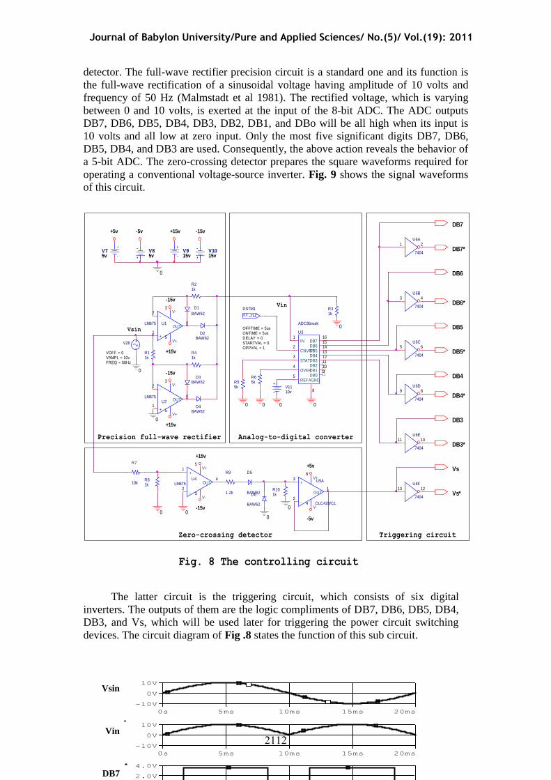
4. 1 The controlling circuit This circuit is shown in Fig. 8. It consists of three sub circuits, which are the
precision full-wave rectifier, analog-to-digital converter, and the zero-crossing
Journal of Babylon University/Pure and Applied Sciences/ No.(5)/ Vol.(19): 2011
4004
detector. The full-wave rectifier precision circuit is a standard one and its function is
the full-wave rectification of a sinusoidal voltage having amplitude of 10 volts and
frequency of 50 Hz (Malmstadt et al 1981). The rectified voltage, which is varying
between 0 and 10 volts, is exerted at the input of the 8-bit ADC. The ADC outputs
DB7, DB6, DB5, DB4, DB3, DB2, DB1, and DBo will be all high when its input is
10 volts and all low at zero input. Only the most five significant digits DB7, DB6,
DB5, DB4, and DB3 are used. Consequently, the above action reveals the behavior of
a 5-bit ADC. The zero-crossing detector prepares the square waveforms required for
operating a conventional voltage-source inverter. Fig. 9 shows the signal waveforms
of this circuit.
The latter circuit is the triggering circuit, which consists of six digital
inverters. The outputs of them are the logic compliments of DB7, DB6, DB5, DB4,
DB3, and Vs, which will be used later for triggering the power circuit switching
devices. The circuit diagram of Fig .8 states the function of this sub circuit.
Time
0s 5ms 10ms 15ms 20ms
V(V26:+)
-10V
0V
10V
Time
0s 5ms 10ms 15ms 20ms
V(R90:2)
-10V
0V
10V
Time
0s 5ms 10ms 15ms 20ms
V(D4)
0V
2.0V
4.0V
Time
0s 5ms 10ms 15ms 20ms
V(D3)
0V
2.0V
4.0V
Time
0s 5ms 10ms 15ms 20ms
V(D2)
0V
2.0V
4.0V
Time
0s 5ms 10ms 15ms 20ms
V(D1)
0V
2.0V
4.0V
Time
0s 5ms 10ms 15ms 20ms
V(DO)
0V
2.0V
4.0V
Time
0s 5ms 10ms 15ms 20ms
V(VS)
0V
2.5V
5.0V
Vsin
Vin
DB7
Triggering circuit
DB7
DB7*
Vs*
Vin
Fig. 8 The controlling circuit
Vs
U6A
7404
1 2
DB6
U6B
7404
3 4
DB5
U6C
7404
5 6
U6D
7404
9 8
DB4
U6E
7404
11 10
DB3
U6F
7404
13 12
Vsin0
Analog-to-digital converter
U3
ADC8break
DB716
DB615
DB514
DB413
DB312
DB211
DB110
DB09
AGND
8
IN1
CNVRT2
STAT3
OVER4
REF5
0
R55k
R65k
V1110v
000
CLK
DSTM1
OFFTIME = 5usONTIME = 5usDELAY = 0STARTVAL = 0OPPVAL = 1
+5v
0
+15v
R101k
-15v0
U4LM675
+1
-2
V+5
V-3
OUT4
0
R7
10kR81k
R9
1.2k
D5
BAW62D6
BAW62
0 -5v
V75v
-5v+5v
V85v
V915v
V1015v
+15v -15v
0
+15v
0
-15v
V26
FREQ = 50HzVAMPL = 10vVOFF = 0
-15v
+15v
R11k
R41k
R21k
D2BAW62
D4BAW62
0
U1LM675
+1
-2
V+5
V-3
OUT4
U2LM675
+1
-2
V+5
V-3
OUT4
DB6*D1
BAW62
D3BAW62
Zero-crossing detector
Precision full-wave rectifier
U5A
CLC428/CL
OUT1
V+8
V-4
+3
-2
DB5*
R31k
DB4*
DB3*

4002
4. 2 The driving circuit The diving circuit includes fourteen identical sub circuits as obviously indicated
in the whole circuit diagram shown in Fig. 7. Each sub circuit is designed according
to the datasheet of the switching device to be driven which is an insulated-gate bipolar
transistor (IGBT) of the type IRGBC40F. Fig. 10 shows the driving circuit of the
IGBT Z5. The resistance RON is chosen to be greater than ROFF for forbidding the
instantaneous commutation of toggling IGBT’s by completing the turning off for a
certain IGBT before the conduction of the other (Rashid 2001). For example the
IGBT’s Z1 and Z1* are two toggling switching devices and hence when one of them
Fig. 10 The driving circuit of the IGBT Z*5.
Q1
Q2N3904
C5
Q2Q2N3904R14
1k
RON50 ohms
DB7*
0
ROFF5 ohms
GZ5*Q3
Q2N3906
U8A
CLC428/CL
OUT1
V+
8V
-4
+3
-2
-5v
+5v
R125k
R135k
R11
22
V12 15v
U9
A4N25A
Journal of Babylon University/Pure and Applied Sciences/ No.(5)/ Vol.(19): 2011
4002
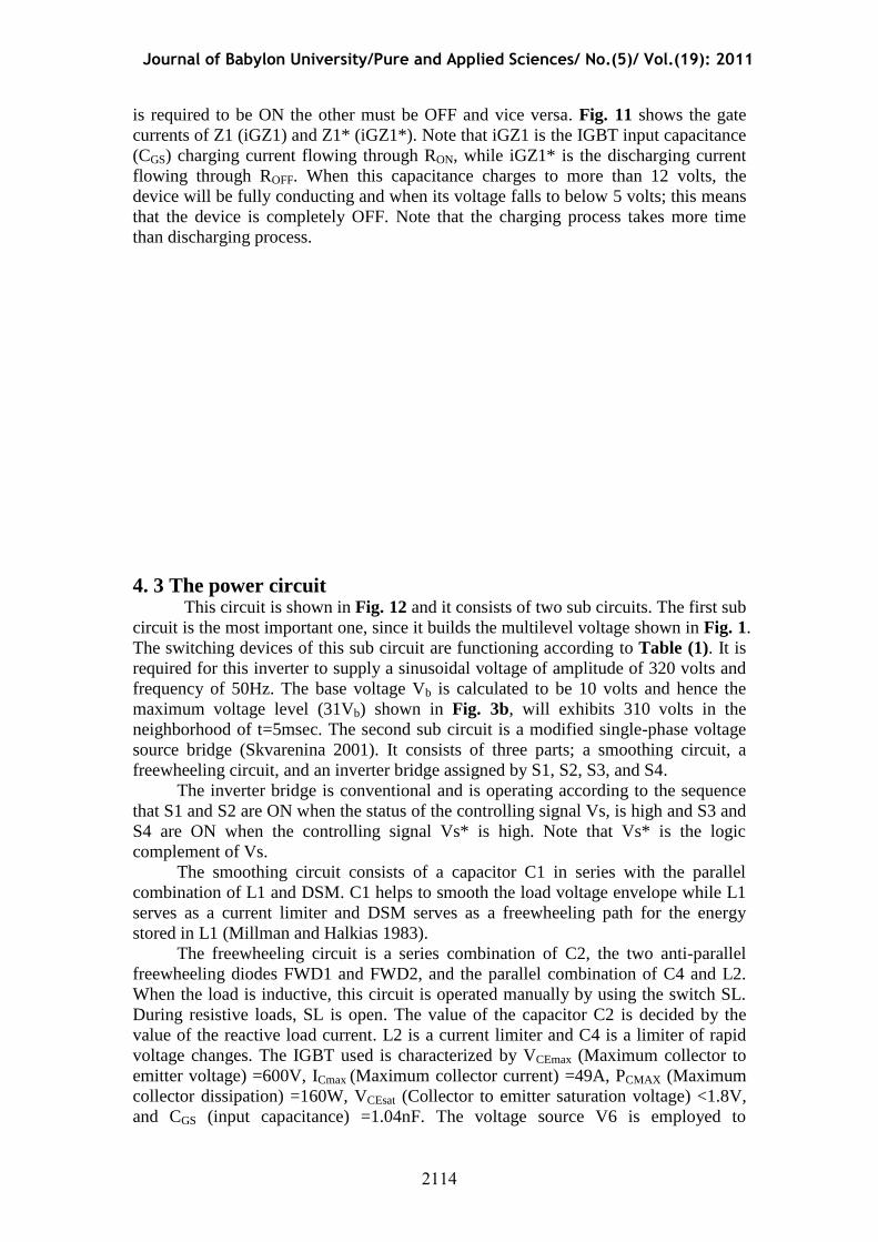
is required to be ON the other must be OFF and vice versa. Fig. 11 shows the gate
currents of Z1 (iGZ1) and Z1* (iGZ1*). Note that iGZ1 is the IGBT input capacitance
(CGS) charging current flowing through RON, while iGZ1* is the discharging current
flowing through ROFF. When this capacitance charges to more than 12 volts, the
device will be fully conducting and when its voltage falls to below 5 volts; this means
that the device is completely OFF. Note that the charging process takes more time
than discharging process.
4. 3 The power circuit This circuit is shown in Fig. 12 and it consists of two sub circuits. The first sub
circuit is the most important one, since it builds the multilevel voltage shown in Fig. 1.
The switching devices of this sub circuit are functioning according to Table (1). It is
required for this inverter to supply a sinusoidal voltage of amplitude of 320 volts and
frequency of 50Hz. The base voltage Vb is calculated to be 10 volts and hence the
maximum voltage level (31Vb) shown in Fig. 3b, will exhibits 310 volts in the
neighborhood of t=5msec. The second sub circuit is a modified single-phase voltage
source bridge (Skvarenina 2001). It consists of three parts; a smoothing circuit, a
freewheeling circuit, and an inverter bridge assigned by S1, S2, S3, and S4.
The inverter bridge is conventional and is operating according to the sequence
that S1 and S2 are ON when the status of the controlling signal Vs, is high and S3 and
S4 are ON when the controlling signal Vs* is high. Note that Vs* is the logic
complement of Vs.
The smoothing circuit consists of a capacitor C1 in series with the parallel
combination of L1 and DSM. C1 helps to smooth the load voltage envelope while L1
serves as a current limiter and DSM serves as a freewheeling path for the energy
stored in L1 (Millman and Halkias 1983).
The freewheeling circuit is a series combination of C2, the two anti-parallel
freewheeling diodes FWD1 and FWD2, and the parallel combination of C4 and L2.
When the load is inductive, this circuit is operated manually by using the switch SL.
During resistive loads, SL is open. The value of the capacitor C2 is decided by the
value of the reactive load current. L2 is a current limiter and C4 is a limiter of rapid
voltage changes. The IGBT used is characterized by VCEmax (Maximum collector to
emitter voltage) =600V, ICmax (Maximum collector current) =49A, PCMAX (Maximum
collector dissipation) =160W, VCEsat (Collector to emitter saturation voltage) <1.8V,
and CGS (input capacitance) =1.04nF. The voltage source V6 is employed to

4002
iFWC
GS1
GZ3*
GS2
SL
C1
Z5* IRGBC40F
Z4* IRGBC40F
DS2
HFA25TB60
31
Z3* IRGBC40F
DS4
HFA25TB60
31
Z2* IRGBC40F
Z1* IRGBC40F
L2
5uH
S1
IRGBC40F
S4
IRGBC40F
C5
GZ2*
FWD2
HFA25TB60
3 1
S2
IRGBC40F
Smoothing circuit
GS4
GZ1*
iL
C4
GZ5
Compensating voltage 0
GZ4
GS3
GZ2
GZ3
GZ1
V110v
S3
IRGBC40F
V220v
V340v
V480v L
C3
C4
1uF
V5160v
DS1
HF
A2
5T
B6
0
31 DS3
HF
A2
5T
B6
03
1
Fig. 12 The power circuit of the 31-level single-phase voltage source inverter.
R
+
Z10
IRGBC40F
-
A
Z2IRGBC40F
VL
C2
Z3IRGBC40F
B
Z4IRGBC40F
GZ5*
Z5IRGBC40F
GZ4*
C2
150uF
Load
Freewheeling circuit
iSm
C110uF
DSM
HF
A2
5T
B6
0
31
0
L1
10uH
FWD1
HFA25TB6031
V6 10V
0
Vlmt
+
-0
The 31-level voltage supply modified single-phase voltage source inverter
compensate for the total voltage drop across the conducting IGBTs (seven IGBTs are
conducting at the same time). Ten volts for this source is sufficient for compensation.
5. Results The system was tested on PSpice at 27C
o for both resistive and inductive loads.
For resistive loads, the inverter operating frequency was 50Hz, the rms load voltage
required was 220 volts, and the rated load impedance was 10 ohms. For inductive load
loads, the inverter frequency was changed in the range of 25Hz to 75Hz and the load
voltage was changed in such a manner that a constant voltage to frequency ratio was
guaranteed during ac drive applications, which required constant torques. The load
voltage value can be controlled by adjusting the value of the base voltage Vb within
voltage sources V1, V2, V3, V4, and V5. This action can be achieved automatically,
if controlled rectifiers produce these five sources. Fig. 13 shows the voltage and
current waveforms associating two different resistive loads. Fig. 14 shows two
inductive loads operating at nominal frequency (50Hz) and rated voltage (220 volts
rms) with a power factor of 0.8. The first load is running at full load while the second
is running at half-full load.
Time
0s 10ms 20ms 30ms
V(A,B)
-400V
0V
400V
Time
0s 10ms 20ms 30ms
V(C1)
0V
200V
400V
Time
0s 10ms 20ms 30ms
I(R)
-40A
0A
40A
Time
0s 10ms 20ms 30ms
-I(C2)
-40A
0A
40A
Time
0s 10ms 20ms 30ms
V(A,B)
-400V
0V
400V
Time
0s 10ms 20ms 30ms
I(R)
-20A
0A
20A
Time
0s 10ms 20ms 30ms
-I(C2)
-40A
0A
40A
Time
0s 10ms 20ms 30ms
V(C1)
0V
200V
400V
Vmlt Vmlt
VL VL

Journal of Babylon University/Pure and Applied Sciences/ No.(5)/ Vol.(19): 2011
4002
Fig. 15 shows voltage and current waveforms for a load running at 25Hz, 50Hz,
and 75Hz. For the three load conditions, voltage to frequency ratio was kept constant
by changing Vb for each case. Vb was adjusted to 5 volts, when the required frequency
f was 25Hz and adjusted to 15 volts when f was 75Hz. The load impedance ZL in that
Time
0s 10ms 20ms 30ms
V(C1)
-400V
0V
400V
Time
0s 10ms 20ms 30ms
V(A,B)
-400V
0V
400V
Time
0s 10ms 20ms 30ms
I(R)
-40A
0A
40A
Time
0s 10ms 20ms 30ms
-I(C2)
-10A
0A
10A
Time
0s 10ms 20ms 30ms
-I(C1)
-25A
0A
25A
50A
Time
0s 10ms 20ms 30ms
V(C1)
-400V
0V
400V
Time
0s 10ms 20ms 30ms
V(A,B)
-400V
0V
400V
Time
0s 10ms 20ms 30ms
I(R)
-20A
0A
20A
Time
0s 10ms 20ms 30ms
-I(C2)
-10A
0A
10A
Time
0s 10ms 20ms 30ms
-I(C1)
-20A
0A
20A
VL VL
Vmlt Vmlt
iL iL
iSM iSM
iFWD iFWD
(a) (b)
Fig. 14 Voltage and current waveforms for a 0.8 p.f inductive load, (a) ZL=10Ω,
(b) ZL=20Ω.

4002
Fig. 16 voltage to frequency rato under ac
drive operation.
0
1
2
3
4
5
6
7
0 10 20 30 40 50 60 70 80
Frequency
Vo
ltag
e t
o f
req
uen
cy
rati
o
case had R=8.5Ω and L=16.8mH. Consequently, ZL was calculated to be 8.9Ω for
f=25Hz, 10Ω for f=50Hz, and 11.61Ω for f=75Hz. The power factor values for those
cases were 0.955, 0.85, and 0.732.
The voltage to frequency ratio was calculated and plotted against frequency as
shown in Fig. 16. It is obvious that this ratio is almost constant.
5. Conclusion The new approach has succeeded in the production of a sinusoidal voltage
waveform for high power purposes. In addition, it offers the possibility of the
extension to high voltage dc transmission technology where pure sine waves are the
Time
0s 20ms 40ms
V(A,B)
-200V
0V
200V
Time
0s 20ms 40ms
I(R)
-20A
0A
20A
Time
0s 20ms 40ms
V(A,B)
-400V
0V
400V
Time
0s 20ms 40ms
I(R)
-40A
0A
40A
Time
0s 20ms 40ms
V(A,B)
-500V
0V
500V
Time
0s 20ms 40ms
I(R)
-50A
0A
50A
Fig. 15 Voltage and current waveforms for a load having R=8.5Ω and
L=16.8mH under variable ac drive operation.
VL
VL
VL
iL
iL
iL
f=25Hz, Vb=5V
f=50Hz, Vb=10V
f=75Hz,
Vb=7.5V

Journal of Babylon University/Pure and Applied Sciences/ No.(5)/ Vol.(19): 2011
4002
utmost aspirations. The three-phase configuration is possible and it will certainly be
the future work of this approach. The fundamental component of the produced voltage
in Table (2) leads to the conclusion that, the best numbers of nonzero levels are
rounded by 15 and 31, which are revealing a good compromise between quality and
economical cost. Since the fundamental component of the 31-level voltage is very
close to the desired voltage amplitude, the harmonic components associating the
generated voltage are almost negligible. The current waveforms for both resistive and
inductive loads reflect sinusoidal behaviors.
This technique is characterized by the reduction of numbers of power voltage
sources and switching devices. The number of voltage sources is reduced to log2 (N+1)
instead of N. Consequently, the number of switching devices will be reduced in the
same manner. It is obvious that this technique is economically utilized.
References Kumar J., Das B., and Agarwal P. (2008) Selective harmonic elimination technique
for a multilevel inverter. Fifteen National Power Systems Conference (NPSC),
December 2008, Bombay, pp 608-613.
Mailah N. F., Bashi S. M., Aris I., and Mariun N. (2009) Neutral-point-clamped
multilevel inverter using Space Vector Modulation. European Journal of
Scientific Research ISSN 1450-216X, 28: 82-91.
Malmstadt H. V., Enke C. G., Crouch S. R. (1981) Electronics and instrumentation for
scientists. Th Benjamin/ Cumming Company, Inc, pp 543.
Manguelle J. S. and Rufer A. (2001) Asymmetrical multilevel inverter for large
induction machine drives. Electrical Drives and Power Electronics International
Conference, October 3-5, Slovakia pp 101-107.
Mekhilef S. and Masaoud A. (2006) Xilinx FPGA based multilevel PWM single
phase inverter. Online at http:#ejum.fsktm.um.my © 2006 Engineering e-
Transction, University of Malaya, 1: 40-45.
Millman J. and Halkias C. (1983) Integrated electronics: analogue and digital circuits
and systems. McGraw-Hill, Inc, pp 911.
Pandian G. and Reddy S. R. (2008) Implementation of multilevel inverter-induction
motor drive. Journal of Industrial Technology, 24: 1-6.
Rashid M. (2001) Power electronics handbook. Academic Press, pp 892.
Skvarenina T. (2001) The power electronics handbook. CRC Press, pp 626.
Teodorescu R., Blaabjerg F., Pedersen J. K., Cengelci E., and Enjeti P. N. (2002)
Multilevel inverter by cascading industrial VSI. IEEE Transactions on Industrial
Tolbert L. M. and Habetler T. G. (1999) Novel multilevel inverter-carrier based PW
Mmethod. IEEE Transactions on Industry Applications, 35: 1098-1106.
Wylie C. R. (1975) Advanced engineering mathematics. McGraw-Hill, Inc, pp 937.


![INVERTER POWER CONTROL BASED ON DC-LINK VOLTAGE …compared with phase of grid voltage. Lee et al. [3] proposed a novel control scheme of single-phase-to-three-phase Pulse Width-Modulation](https://img.pdfslide.us/doc/110x75/5eb9b0447f3e6e72a955e644/inverter-power-control-based-on-dc-link-voltage-compared-with-phase-of-grid-voltage.jpg)